US8994855B2 - CMOS pixel control method - Google Patents
CMOS pixel control method Download PDFInfo
- Publication number
- US8994855B2 US8994855B2 US13/930,874 US201313930874A US8994855B2 US 8994855 B2 US8994855 B2 US 8994855B2 US 201313930874 A US201313930874 A US 201313930874A US 8994855 B2 US8994855 B2 US 8994855B2
- Authority
- US
- United States
- Prior art keywords
- integration period
- pixel
- beginning
- photodiode
- sense node
- Prior art date
- Legal status (The legal status is an assumption and is not a legal conclusion. Google has not performed a legal analysis and makes no representation as to the accuracy of the status listed.)
- Expired - Fee Related, expires
Links
Images


Classifications
-
- H—ELECTRICITY
- H04—ELECTRIC COMMUNICATION TECHNIQUE
- H04N—PICTORIAL COMMUNICATION, e.g. TELEVISION
- H04N25/00—Circuitry of solid-state image sensors [SSIS]; Control thereof
-
- H04N5/335—
-
- H—ELECTRICITY
- H04—ELECTRIC COMMUNICATION TECHNIQUE
- H04N—PICTORIAL COMMUNICATION, e.g. TELEVISION
- H04N25/00—Circuitry of solid-state image sensors [SSIS]; Control thereof
- H04N25/50—Control of the SSIS exposure
- H04N25/57—Control of the dynamic range
- H04N25/571—Control of the dynamic range involving a non-linear response
- H04N25/575—Control of the dynamic range involving a non-linear response with a response composed of multiple slopes
-
- H—ELECTRICITY
- H04—ELECTRIC COMMUNICATION TECHNIQUE
- H04N—PICTORIAL COMMUNICATION, e.g. TELEVISION
- H04N25/00—Circuitry of solid-state image sensors [SSIS]; Control thereof
- H04N25/50—Control of the SSIS exposure
- H04N25/57—Control of the dynamic range
-
- H—ELECTRICITY
- H04—ELECTRIC COMMUNICATION TECHNIQUE
- H04N—PICTORIAL COMMUNICATION, e.g. TELEVISION
- H04N25/00—Circuitry of solid-state image sensors [SSIS]; Control thereof
- H04N25/50—Control of the SSIS exposure
- H04N25/57—Control of the dynamic range
- H04N25/58—Control of the dynamic range involving two or more exposures
- H04N25/581—Control of the dynamic range involving two or more exposures acquired simultaneously
- H04N25/583—Control of the dynamic range involving two or more exposures acquired simultaneously with different integration times
-
- H—ELECTRICITY
- H04—ELECTRIC COMMUNICATION TECHNIQUE
- H04N—PICTORIAL COMMUNICATION, e.g. TELEVISION
- H04N25/00—Circuitry of solid-state image sensors [SSIS]; Control thereof
- H04N25/50—Control of the SSIS exposure
- H04N25/57—Control of the dynamic range
- H04N25/58—Control of the dynamic range involving two or more exposures
- H04N25/587—Control of the dynamic range involving two or more exposures acquired sequentially, e.g. using the combination of odd and even image fields
- H04N25/589—Control of the dynamic range involving two or more exposures acquired sequentially, e.g. using the combination of odd and even image fields with different integration times, e.g. short and long exposures
-
- H—ELECTRICITY
- H04—ELECTRIC COMMUNICATION TECHNIQUE
- H04N—PICTORIAL COMMUNICATION, e.g. TELEVISION
- H04N25/00—Circuitry of solid-state image sensors [SSIS]; Control thereof
- H04N25/60—Noise processing, e.g. detecting, correcting, reducing or removing noise
- H04N25/62—Detection or reduction of noise due to excess charges produced by the exposure, e.g. smear, blooming, ghost image, crosstalk or leakage between pixels
- H04N25/621—Detection or reduction of noise due to excess charges produced by the exposure, e.g. smear, blooming, ghost image, crosstalk or leakage between pixels for the control of blooming
- H04N25/623—Detection or reduction of noise due to excess charges produced by the exposure, e.g. smear, blooming, ghost image, crosstalk or leakage between pixels for the control of blooming by evacuation via the output or reset lines
-
- H—ELECTRICITY
- H04—ELECTRIC COMMUNICATION TECHNIQUE
- H04N—PICTORIAL COMMUNICATION, e.g. TELEVISION
- H04N3/00—Scanning details of television systems; Combination thereof with generation of supply voltages
- H04N3/10—Scanning details of television systems; Combination thereof with generation of supply voltages by means not exclusively optical-mechanical
- H04N3/14—Scanning details of television systems; Combination thereof with generation of supply voltages by means not exclusively optical-mechanical by means of electrically scanned solid-state devices
- H04N3/15—Scanning details of television systems; Combination thereof with generation of supply voltages by means not exclusively optical-mechanical by means of electrically scanned solid-state devices for picture signal generation
- H04N3/155—Control of the image-sensor operation, e.g. image processing within the image-sensor
-
- H04N5/2175—
-
- H04N5/355—
-
- H04N5/35536—
-
- H04N5/35554—
-
- H04N5/35581—
-
- H04N5/3594—
Definitions
- the present disclosure relates to image sensors, including CMOS sensors with a multiple integration period, called high-dynamics sensors, and to methods of controlling pixels of such sensors.
- a CMOS image sensor pixel essentially comprises a photodiode used in reverse mode, having its junction capacitance discharged by a photocurrent according to a received light intensity.
- the measurement of the illumination level received by a pixel is performed by measurement of the voltage across the photodiode at selected times, among which the end of a so-called image acquisition or integration period, before and after which the pixel is reset by recharging of its photodiode.
- the decrease of the voltage across the photodiode during the integration is proportional to the received light intensity.
- the photocurrent may be such that the discharge of the junction capacitance during the integration phase adversely affects the measurement.
- the photodiode reaches, before the end of the integration time, a so-called saturation discharge level, and brightness differences are no longer discriminated.
- control methods with a multiple integration period, that is, comprising several read steps at different times of a same integration phase, have been provided. Such methods enable to extend the dynamic range of the sensor, but however have the disadvantage of introducing unwanted noise into the images.
- An embodiment provides a method for controlling a CMOS pixel, which facilitates addressing at least some of the disadvantages of existing control methods.
- An embodiment provides a multiple integration period control method, which facilitates introducing less unwanted noise into the images than existing methods.
- An embodiment provides a method for controlling a pixel comprising at least one photodiode capable of being connected to a sense node, the method comprising the steps of: a) at the beginning and at the end of a first integration period comprised within a second integration period, controlling the pixel to transfer the charges stored in the photodiode above a first threshold onto the sense node; and b) at an intermediate time between the beginning of the second period and the beginning of the first period, controlling the pixel to transfer the charges stored in the photodiode above the first threshold onto the sense node.
- a time interval substantially equal to the first period separates the intermediate time from the beginning of the first period.
- control method further comprises, between the beginning of the second period and the intermediate time, one or several additional pixel control steps to transfer the charges stored in the photodiode above the first threshold onto the sense node.
- the pixel is controlled to evacuate towards a power supply rail the charges transferred from the photodiode to the sense node at the beginning of the first integration period.
- control method further comprises a step of measurement of information representative of the amount of charges transferred from the photodiode to the sense node at the end of the first integration period.
- the pixel is controlled to evacuate towards a power supply rail the charges transferred from the photodiode to the sense node at the intermediate time.
- control method further comprises a step of control of the pixel to transfer the charges stored in the photodiode onto the sense node at the end of the second integration period.
- control method further comprises a step of measurement of information representative of the amount of charges transferred from the photodiode to the sense node at the end of the second integration period.
- the photodiode is connected to the sense node via a MOS transistor, and the transfers are controlled by applying a pulse to the transistor gate.
- An embodiment provides an image acquisition device, comprising: a plurality of pixels each comprising a photodiode capable of being connected to a sense node; and control circuits configured to control the pixels according to the above-mentioned control method.
- a method may comprise: reading a pixel during a first integration period; reading the pixel between an end of the first integration period and an end of a second integration period, the second integration period including the first integration period; reading the pixel after the end of a second integration period; at a beginning and at the end of the first integration period, causing the pixel to transfer charge stored in a photodiode above a first threshold onto a sense node; and at an intermediate time between a beginning of the second integration period and the beginning of the first integration period, causing the pixel to transfer charge stored in the photodiode above the first threshold onto the sense node.
- a time interval substantially equal to the first integration period may separate said intermediate time from the beginning of the first integration period.
- the method may include, at least once between the beginning of the second period and said intermediate time, causing the pixel to transfer charge stored in the photodiode above the first threshold onto the sense node.
- the method may comprises evacuating towards a power supply charge transferred from the photodiode onto the sense node at the beginning of the first integration period.
- the method may comprise evacuating towards a power supply charge transferred from the photodiode to the sense node at said intermediate time.
- the method may comprise transferring charge stored in the photodiode onto the sense node at the end of the second integration period.
- the photodiode may be connected to the sense node via a MOS transistor, and said transfers may be controlled by applying a pulse to a gate of the MOS transistor.
- a device may comprise: a read signal generator configured to generate a pixel-read signal to cause a pixel to be read: during a first integration period; between an end of a first integration period and an end of a second integration period, the second integration period including the first integration period; and after the end of the second integration period; and a transfer signal generator configured to generate a pixel-charge-transfer signal at a beginning and at an end of the first integration period, and at an intermediate time between a beginning of the second integration period and the beginning of the first integration period.
- the device may comprise a reset signal generator configured to generate a pixel-reset signal.
- the device may comprises an image data generator configured to generate image data based on data received in response to data read signals.
- the device may comprise a pixel configured to receive the pixel-read signal and the pixel-charge-transfer signal.
- the pixel-charge-transfer signal may cause the pixel to transfer charge stored in a photodiode above a first threshold onto a pixel sense node.
- a time interval substantially equal to the first integration period may separate said intermediate time from the beginning of the first integration period.
- the transfer signal generator may be configured to generate a pixel-charge-transfer signal at least once between the beginning of the second period and said intermediate time.
- the transfer signal generator may be configured to generate a pixel-charge transfer signal at the end of the second integration period.
- the device may comprise a pixel, the pixel including a photodiode coupled to a sense node via a MOS transistor, wherein the pixel-charge-transfer signal is a pulse applied to a gate of the MOS transistor.
- a system may comprise: a pixel array: a read signal generator configured to generate one or more signals to cause at least one pixel of the pixel array to be read: during a first integration period; between an end of a first integration period and an end of a second integration period, the second integration period including the first integration period; and after the end of the second integration period; and a transfer signal generator configured to generate a pixel-charge-transfer signal to cause at least one pixel of the pixel array to transfer charge stored in a photodiode above a first threshold onto a pixel sense node at a beginning and at an end of the first integration period, and at an intermediate time between a beginning of the second integration period and the beginning of the first integration period.
- the system may comprise a reset signal generator configured to generate a pixel-reset signal to cause at least one pixel of the pixel array to reset.
- the system may comprise an image data generator configured to generate image data based on data received from the pixel array in response to data read signals.
- a time interval substantially equal to the first integration period may separate said intermediate time from the beginning of the first integration period.
- a non-transitory computer-readable medium may contain contents to configure a controller to perform a method, the method comprising: reading a pixel during a first integration period; reading the pixel between an end of the first integration period and an end of a second integration period, the second integration period including the first integration period; reading the pixel after the end of a second integration period; at a beginning and at the end of the first integration period, causing the pixel to transfer charge stored in a photodiode above a first threshold onto a sense node; and at an intermediate time between a beginning of the second integration period and the beginning of the first integration period, causing the pixel to transfer charge stored in the photodiode above the first threshold onto the sense node.
- a time interval substantially equal to the first integration period may separate said intermediate time from the beginning of the first integration period.
- the method may comprise, at least once between the beginning of the second period and said intermediate time, causing the pixel to transfer charge stored in the photodiode above the first threshold onto the sense node.
- a system may comprise: means for reading at least one pixel: during a first integration period; between an end of a first integration period and an end of a second integration period, the second integration period including the first integration period; and after the end of the second integration period; and means for causing the at least one pixel to transfer charge stored in a photodiode above a first threshold onto a pixel sense node at a beginning and at an end of the first integration period, and at an intermediate time between a beginning of the second integration period and the beginning of the first integration period.
- the system may comprise a pixel array coupled to the means for reading and the means for causing the at least one pixel to transfer charge.
- the system may comprise means for resetting the at least one pixel.
- the system may comprise means for generating image data.
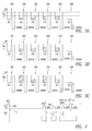
- FIG. 1 illustrates an electric diagram of an example of CMOS image sensor pixel
- FIG. 2 is a timing diagram illustrating the variation of signals for controlling the pixel of FIG. 1 , according to an example of control method with a double integration period;
- FIGS. 3A to 3C schematically illustrate charge transfers from a photodiode to a sense node of the pixel of FIG. 1 , when this pixel is controlled according to the method of FIG. 2 ;
- FIG. 4 is a timing diagram illustrating the variation of signals for controlling the pixel of FIG. 1 , according to an embodiment of control method with a double integration period;
- FIG. 5 is a functional block diagram of a pixel sensor system.
- FIG. 1 illustrates, as an example, an electric diagram of a pixel 100 of a CMOS image sensor.
- Pixel 100 comprises a photodiode 101 having its anode connected to a reference node, as illustrated a low power supply rail, generally the ground, and having its cathode K, or acquisition node, connected, via a transfer transistor 103 , to a sense node SENSE.
- Sense node SENSE is connected, by a reset transistor 105 , to a supply node, as illustrated, a high power supply rail V RT .
- Node SENSE is further connected to the gate of a transistor 107 configured as a follower source.
- transistor 107 The drain of transistor 107 is connected to high power supply rail V RT , and the source of transistor 107 is connected, via a read transistor 109 , to a bit line 110 of an array network comprising the pixel.
- transistors 103 , 105 , 107 , and 109 are N-channel MOS transistors.
- FIGS. 2 and 3A to 3 C illustrate the operation of an example of a control method with a double integration period, which has been provided to improve the discrimination of brightness levels.
- FIG. 2 is a timing diagram illustrating the variation of control signals TG and RST respectively applied to the gate of transfer transistor 103 and to the gate of reset transistor 105 of pixel 100 of FIG. 1 .
- signal RST is set to a high state, which causes the setting of the voltage of sense node SENSE to high power supply voltage V RT .
- Transfer signal TG is then set to a high voltage V HTG , for example, equal to 2.8 V, during a first pulse 201 , or initialization pulse. This causes the transfer of all the charges stored in photodiode 101 to sense node SENSE, and their evacuation towards the high power supply rail via transistor 105 .
- the voltage across photodiode 101 then becomes equal to the natural voltage of the diode, which results from the doping levels, for example, on the order of 1.5 V.
- Falling edge 202 of pulse 201 marks the beginning of the integration phase, or long integration period T l .
- acquisition node K is isolated from sense node SENSE (signal TG in the low state), and sense node SENSE is connected to high power supply voltage V RT (signal RST in the high state).
- V RT signal RST in the high state.
- Node SENSE being isolated from high power supply rail V RT (signal RST in the low state), the voltage of node SENSE decreases accordingly. If, however, during the second pulse, the voltage at node K is greater than V MD , no current flows through transistor 103 and the voltages of node K and of node SENSE remain unchanged. After second pulse 203 , signal RST is set back to the high state, which resets the voltage of node SENSE to high power supply voltage V RT .
- Falling edge 204 of second pulse 203 marks the beginning of a short integration period T s , comprised within long integration period T l , during which the voltage across the photodiode keeps on decreasing proportionally to the amount of light received by the pixel.
- signal RST is set to a low state to isolate sense node SENSE from high power supply rail V RT .
- the voltage of node SENSE is then read, as illustrated by arrow LREF of FIG. 2 , for example by turning on read transistor 109 to transfer the voltage of node SENSE towards the pixel output via transistor 107 assembled as a follower source.
- Voltage V LREF read at step LREF is stored and forms a reference for subsequent steps of measurement of the photodiode discharge level.
- a third pulse 205 or first read pulse, of same voltage level V MTG as second pulse 203 , is applied to signal TG. If, during the third pulse, the voltage at acquisition node K is at a level lower than V MD , a current flows through transistor 103 , taking the voltage of node K back to level V MD . Node SENSE being isolated from high power supply rail V RT (signal RST in the low state), the voltage of node SENSE decreases accordingly. If, however, during the third pulse, the voltage of node K is greater than V MD , the voltage of K and the voltage of node SENSE remain unchanged.
- a fourth pulse 207 is applied to signal TG, at a voltage equal to voltage V HTG of first pulse 201 , for example, 2.8 V. This causes the transfer to sense node SENSE of all the photogenerated charges remaining in photodiode 101 .
- the voltage of node SENSE which has not been reset after first read pulse 205 , decreases by a value proportional to the transferred amount of charges.
- the voltage of sense node SENSE is read, as indicated by arrow L 2 of FIG. 2 .
- the final output value of the pixel is equal to the maximum value between V LREF ⁇ V L2 and (V LREF ⁇ V L1 )*(T l /T s ).
- the pixel is reset for a new integration phase.
- FIGS. 3A to 3C schematically illustrate charge transfers from acquisition node K to sense node SENSE of pixel 100 of FIG. 1 , when the pixel is controlled according to the method of FIG. 2 .
- FIGS. 3A , 3 B, and 3 C show the transfers respectively in the case of a low illumination, in the case of a medium illumination, and in the case of a strong illumination.
- photodiode 101 and sense node SENSE contain no photogenerated charges.
- photodiode 101 contains an amount of photogenerated charges proportional to the light intensity received by the pixel from the beginning of the integration.
- photogenerated charges stored in the photodiode during the short integration period add to the charges remaining in the photodiode after the application of skimming pulse 203 .
- the amount of new photogenerated charges is proportional to the light intensity received from the beginning of short integration period T s .
- the charges stored in the photodiode above the intermediate threshold set by voltage V MD are transferred to sense node SENSE.
- Node SENSE being isolated from high power supply voltage V RT , the transferred charges remain stored on node SENSE.
- the voltage of node SENSE thus decreases by a value proportional to the transferred amount of charges.
- no charge is transferred to node SENSE in the case of the low illumination and charges are transferred in the case of medium or strong illuminations.
- the voltage of node SENSE is then measured (read step L 1 of FIG. 2 ), which provides information representative of the transferred amount of charges.
- control method of FIG. 2 enables to improve the brightness level discrimination and accordingly to extend the dynamic range of the sensor. This method however has the disadvantage of introducing unwanted noise into images.
- skimming pulse 203 in pixels receiving a medium to strong brightness (and generally in pixels where skimming pulse 203 effectively causes the evacuation of part of the charges stored in the photodiode), the amount of charges remaining in the photodiode after the application of a pulse 203 or 205 depends on the amount of charges contained in the photodiode just before the pulse.
- skimming pulse 203 generally occurs in the final portion of long integration period T s .
- the photodiode may be strongly saturated at the time when skimming pulse 203 is applied.
- period T s being relatively short, the photodiode is generally not saturated at the time when first read pulse 205 is applied (except in case of a very high light intensity).
- This difference in the photodiode discharge state just before the application of pulses 203 and 205 results in that the amount of charges stored in the photodiode at the beginning of short integration period T s does not always exactly correspond to the amount of charges remaining in the photodiode after first read pulse 205 , which causes the above-mentioned poor linearity.
- FIG. 4 is a timing diagram illustrating the operation of an embodiment of a control method with a double integration period.
- FIG. 4 more specifically illustrates the variation of control signals TG and RST respectively applied to the gate of transfer transistor 103 and to the gate of reset transistor 105 of pixel 100 of FIG. 1 .
- signal TG comprises the same pulses as in the example of FIG. 2 , that is, an initialization pulse 201 at the beginning of a long integration period T l , a skimming pulse 203 at the beginning of a short integration period T s comprised within long integration period T l , a first read pulse 205 at the end of short integration period T s , and a second read pulse 207 at the end of long integration period T l .
- signal TG further comprises, after the beginning of long integration period T l but before skimming pulse 203 , an intermediate skimming pulse 403 , at the same voltage V MTG as pulses 203 and 205 , for example 1.4 V.
- signal RST is set to the low state just before intermediate skimming pulse 403 , and is then set back to the high state just after pulse 403 .
- the variation of signal RST is the same as in the example of FIG. 2 .
- Pulse 403 does not mark the beginning or the end of an integration period and is associated to no step of reading of the voltage of node SENSE but, except in cases of extreme brightness, enables the photodiode not to be saturated at the starting of skimming pulse 203 marking the beginning of short integration period T s .
- the pixel substantially behaves in the same way during the application of skimming pulse 203 and during the application of first read pulse 205 .
- the provision of pulse 403 enables, in cases of a medium to strong brightness, to match at best the amount of charges remaining in the photodiode just after skimming pulse 203 and the amount of charges remaining in the photodiode just after first read pulse 205 . This enables to suppress the above-mentioned linearity problems, and accordingly the parasitic noise introduced into the image.
- the time interval separating intermediate skimming pulse 403 from skimming pulse 203 is on the order of the duration of short integration period T s .
- the amount of photogenerated charges stored in the photodiode between pulse 403 and pulse 203 is substantially identical to the amount of photogenerated charges stored between pulse 203 and pulse 205 .
- duration T e between falling edge 404 of intermediate skimming pulse 403 and falling edge 204 of skimming pulse 203 may range between 0.8 and 1.2 times short integration period T s , and may be equal to period T s .
- intermediate skimming pulses may be provided before pulse 403 , at the same amplitude level V MTG as pulses 403 , 203 , and 205 .
- intermediate skimming pulses may be provided all along the period comprised between the beginning of long integration period T l and pulse 403 , spaced apart from one another by a time period substantially equal to short integration period T s .
- FIG. 5 illustrates an embodiment of a system 500 comprising one or more CMOS pixels 100 coupled to a controller 502 .
- the controller 502 may be configured to generate control signals to control one or more pixels in accordance with one or more of the methods disclosed herein.
- the controller comprises a reset signal generator 504 configured to generate one or more reset signals to control one or more pixels 100 , a transfer signal generator 506 configured to generate one or more transfer signals to control one or more pixels 100 , a read signal generator 508 configured to generate one or more read signals to control one or more pixels 100 , and an optional image data generator 510 configured to generate image data based on information received from one or more pixels.
- the controller 502 may comprise, for example, one or more memories M, one or more processors P, one or more state machines SM, discrete circuitry DCR (e.g., logic gates, multipliers, etc.), etc., and various combinations thereof, configured to implement the generators of the controller 502 , e.g., configured to generate signals to control the CMOS pixels 100 , such as signals TG, RST and READ, and to process outputs generated by the pixels 100 , such as outputs on bit line 110 .
- DCR discrete circuitry
- a computer readable medium comprising a computer program adapted to perform one or more of the methods described above.
- the medium may be a physical storage medium such as for example a Read Only Memory (ROM) chip, or a disk such as a Digital Versatile Disk (DVD-ROM), Compact Disk (CD-ROM), a hard disk, a memory, a network, or a portable media article to be read by an appropriate drive or via an appropriate connection, including as encoded in one or more barcodes or other related codes stored on one or more such computer-readable mediums and being readable by an appropriate reader device.
- ROM Read Only Memory
- DVD-ROM Digital Versatile Disk
- CD-ROM Compact Disk
- some or all of the systems and/or modules may be implemented or provided in other manners, such as at least partially in firmware and/or hardware, including, but not limited to, one or more application-specific integrated circuits (ASICs), state machines, discrete circuitry, standard integrated circuits, controllers (e.g., by executing appropriate instructions, and including microcontrollers and/or embedded controllers), field-programmable gate arrays (FPGAs), complex programmable logic devices (CPLDs), etc., as well as devices that employ RFID technology.
- ASICs application-specific integrated circuits
- controllers e.g., by executing appropriate instructions, and including microcontrollers and/or embedded controllers
- FPGAs field-programmable gate arrays
- CPLDs complex programmable logic devices
- some of the modules or controllers separately described herein may be combined, split into further modules and/or split and recombined in various manners.
- the systems, modules and data structures may also be transmitted as generated data signals (e.g., as part of a carrier wave) on a variety of computer-readable transmission mediums, including wireless-based and wired/cable-based mediums.
- the present disclosure is not limited to the pixel example described in relation with FIG. 1 . It will occur to those skilled in the art that the method described in relation with FIG. 4 , as well as the method described in relation with FIG. 2 , may be adapted to any CMOS pixel comprising a photodiode capable of being connected to a sense node.
- signal RST is set to the low state during skimming pulse 203 and intermediate skimming pulse 403 .
- This enables to ascertain that the conditions of use of the pixel are the same during skimming phases (pulses 403 and 203 ) and during the first read phase (pulse 205 ), and thus to minimize linearity problems.
- it may be provided to leave signal RST in the high state during pulses 403 and 203 . In this case, the charges transferred to node SENSE during skimming phases 403 and 203 are evacuated towards high power supply rail V RT , without waiting for the end of the skimming phase.
- the present disclosure is not limited to the specific case described in relation with FIG. 4 where the pixel is controlled according to a double integration period method. It will be within the abilities of those skilled in the art to adapt the provided method to the case of a multiple integration period control comprising more than two read steps at different times of a same integration phase, different skimming levels being provided for the different read steps.
Abstract
Description
Claims (31)
Applications Claiming Priority (2)
| Application Number | Priority Date | Filing Date | Title |
|---|---|---|---|
| FR1256319A FR2992813A1 (en) | 2012-07-02 | 2012-07-02 | METHOD FOR CONTROLLING A CMOS PIXEL |
| FR1256319 | 2012-07-02 |
Publications (2)
| Publication Number | Publication Date |
|---|---|
| US20140002705A1 US20140002705A1 (en) | 2014-01-02 |
| US8994855B2 true US8994855B2 (en) | 2015-03-31 |
Family
ID=47172784
Family Applications (1)
| Application Number | Title | Priority Date | Filing Date |
|---|---|---|---|
| US13/930,874 Expired - Fee Related US8994855B2 (en) | 2012-07-02 | 2013-06-28 | CMOS pixel control method |
Country Status (2)
| Country | Link |
|---|---|
| US (1) | US8994855B2 (en) |
| FR (1) | FR2992813A1 (en) |
Families Citing this family (2)
| Publication number | Priority date | Publication date | Assignee | Title |
|---|---|---|---|---|
| FR2996957A1 (en) * | 2012-10-12 | 2014-04-18 | St Microelectronics Grenoble 2 | METHOD FOR READING A PIXEL |
| WO2014144391A1 (en) * | 2013-03-15 | 2014-09-18 | Rambus Inc. | Threshold-monitoring, conditional-reset image sensor |
Citations (11)
| Publication number | Priority date | Publication date | Assignee | Title |
|---|---|---|---|---|
| US6963370B2 (en) * | 2001-09-24 | 2005-11-08 | The Board Of Trustees Of The Leland Stanford Junior University | Method for improving SNR in low illumination conditions in a CMOS video sensor system using a self-resetting digital pixel |
| US20050253945A1 (en) * | 2004-05-13 | 2005-11-17 | Canon Kabushiki Kaisha | Solid-state image pickup device and camera using the same solid-state image pickup device |
| US7394492B2 (en) * | 2003-12-05 | 2008-07-01 | Canon Kabushiki Kaisha | Solid state image pickup device, method of driving solid state image pickup device, and camera using the solid state image pickup device |
| US20080258045A1 (en) * | 2005-10-28 | 2008-10-23 | Sony Corporation | Solid-state imaging device, method of driving solid-state imaging device and imaging apparatus |
| EP2071825A1 (en) | 2007-12-13 | 2009-06-17 | St Microelectronics S.A. | Pixel read circuitry |
| US20110013065A1 (en) | 2009-07-16 | 2011-01-20 | Canon Kabushiki Kaisha | Solid-state imaging apparatus and driving method therefor |
| EP2383980A1 (en) | 2010-03-11 | 2011-11-02 | STmicroelectronics SA | CMOS Image sensor having a wide linear dynamic range |
| US20120075499A1 (en) | 2010-09-28 | 2012-03-29 | Takayoshi Kawaguchi | Image processing apparatus, image processing method, and image processing program |
| US20120086826A1 (en) * | 2005-10-05 | 2012-04-12 | Panasonic Corporation | Solid-state imaging device, imaging apparatus and driving method for the same |
| US8773562B1 (en) * | 2013-01-31 | 2014-07-08 | Apple Inc. | Vertically stacked image sensor |
| US20140247378A1 (en) * | 2013-03-01 | 2014-09-04 | Apple Inc. | Exposure control for image sensors |
-
2012
- 2012-07-02 FR FR1256319A patent/FR2992813A1/en not_active Withdrawn
-
2013
- 2013-06-28 US US13/930,874 patent/US8994855B2/en not_active Expired - Fee Related
Patent Citations (12)
| Publication number | Priority date | Publication date | Assignee | Title |
|---|---|---|---|---|
| US6963370B2 (en) * | 2001-09-24 | 2005-11-08 | The Board Of Trustees Of The Leland Stanford Junior University | Method for improving SNR in low illumination conditions in a CMOS video sensor system using a self-resetting digital pixel |
| US7394492B2 (en) * | 2003-12-05 | 2008-07-01 | Canon Kabushiki Kaisha | Solid state image pickup device, method of driving solid state image pickup device, and camera using the solid state image pickup device |
| US20050253945A1 (en) * | 2004-05-13 | 2005-11-17 | Canon Kabushiki Kaisha | Solid-state image pickup device and camera using the same solid-state image pickup device |
| US20120086826A1 (en) * | 2005-10-05 | 2012-04-12 | Panasonic Corporation | Solid-state imaging device, imaging apparatus and driving method for the same |
| US20080258045A1 (en) * | 2005-10-28 | 2008-10-23 | Sony Corporation | Solid-state imaging device, method of driving solid-state imaging device and imaging apparatus |
| EP2071825A1 (en) | 2007-12-13 | 2009-06-17 | St Microelectronics S.A. | Pixel read circuitry |
| US20110013065A1 (en) | 2009-07-16 | 2011-01-20 | Canon Kabushiki Kaisha | Solid-state imaging apparatus and driving method therefor |
| US8350942B2 (en) * | 2009-07-16 | 2013-01-08 | Canon Kabushiki Kaisha | Solid-state imaging apparatus and driving method therefor |
| EP2383980A1 (en) | 2010-03-11 | 2011-11-02 | STmicroelectronics SA | CMOS Image sensor having a wide linear dynamic range |
| US20120075499A1 (en) | 2010-09-28 | 2012-03-29 | Takayoshi Kawaguchi | Image processing apparatus, image processing method, and image processing program |
| US8773562B1 (en) * | 2013-01-31 | 2014-07-08 | Apple Inc. | Vertically stacked image sensor |
| US20140247378A1 (en) * | 2013-03-01 | 2014-09-04 | Apple Inc. | Exposure control for image sensors |
Also Published As
| Publication number | Publication date |
|---|---|
| FR2992813A1 (en) | 2014-01-03 |
| US20140002705A1 (en) | 2014-01-02 |
Similar Documents
| Publication | Publication Date | Title |
|---|---|---|
| CN105637858B (en) | Matrix image sensor and the method for reading the pixel in matrix image sensor | |
| US7923674B2 (en) | Solid-state image sensor having a voltage applier and signal readout method thereof | |
| TWI281821B (en) | Data processing method, data processing apparatus, semiconductor device for detecting physical quantity distribution, and electronic apparatus | |
| US9148604B2 (en) | Pixel read method | |
| CN105681697A (en) | Image sensor for improving nonlinearity of row code region, and device including the same | |
| CN102695010B (en) | There is the imageing sensor of double integration time and conditional selection | |
| US20090273694A1 (en) | Image sensors and methods with column readout circuits | |
| US8436674B1 (en) | Self-scaled voltage booster | |
| JP4686582B2 (en) | Solid-state imaging device | |
| US9041842B2 (en) | Image sensor pixel cell readout architecture | |
| US9191588B2 (en) | High dynamic range pixel | |
| US9491386B2 (en) | Floating diffusion reset level boost in pixel cell | |
| CN106105181A (en) | There is the dark current of reduction and the image-capturing method of low-power consumption | |
| US20160112662A1 (en) | Image sensor pixel having multiple sensing node gains | |
| KR20120137218A (en) | Pixel and method | |
| US10110783B2 (en) | Image sensor precharge boost | |
| US20090236500A1 (en) | Dark current and lag reduction | |
| US9998693B2 (en) | Image sensor adapted to blinking sources | |
| US20200077081A1 (en) | Method of operating an image sensor, image sensor performing the same, and electronic system including the same | |
| US9635277B2 (en) | Image sensor, image sensing method, and image photographing apparatus including image sensor | |
| US8994855B2 (en) | CMOS pixel control method | |
| US9124836B2 (en) | Image sensor and method of driving the same | |
| CN116349240A (en) | Digital pixel sensor with reduced quantization operation | |
| US11451730B2 (en) | Image sensor using a global shutter and method for controlling same | |
| US10798323B1 (en) | Control method for an active pixel image sensor |
Legal Events
| Date | Code | Title | Description |
|---|---|---|---|
| AS | Assignment |
Owner name: STMICROELECTRONICS (GRENOBLE 2) SAS, FRANCE Free format text: ASSIGNMENT OF ASSIGNORS INTEREST;ASSIGNOR:DESCHAMPS, BENOIT;REEL/FRAME:030795/0746 Effective date: 20130517 |
|
| STCF | Information on status: patent grant |
Free format text: PATENTED CASE |
|
| MAFP | Maintenance fee payment |
Free format text: PAYMENT OF MAINTENANCE FEE, 4TH YEAR, LARGE ENTITY (ORIGINAL EVENT CODE: M1551); ENTITY STATUS OF PATENT OWNER: LARGE ENTITY Year of fee payment: 4 |
|
| FEPP | Fee payment procedure |
Free format text: MAINTENANCE FEE REMINDER MAILED (ORIGINAL EVENT CODE: REM.); ENTITY STATUS OF PATENT OWNER: LARGE ENTITY |
|
| LAPS | Lapse for failure to pay maintenance fees |
Free format text: PATENT EXPIRED FOR FAILURE TO PAY MAINTENANCE FEES (ORIGINAL EVENT CODE: EXP.); ENTITY STATUS OF PATENT OWNER: LARGE ENTITY |
|
| STCH | Information on status: patent discontinuation |
Free format text: PATENT EXPIRED DUE TO NONPAYMENT OF MAINTENANCE FEES UNDER 37 CFR 1.362 |
|
| FP | Lapsed due to failure to pay maintenance fee |
Effective date: 20230331 |