US4598363A - Adaptive delayed polling of sensors - Google Patents

Adaptive delayed polling of sensors Download PDF

Info

Publication number
US4598363A
US4598363A US06/511,742 US51174283A US4598363A US 4598363 A US4598363 A US 4598363A US 51174283 A US51174283 A US 51174283A US 4598363 A US4598363 A US 4598363A
Authority
US
United States
Prior art keywords
sensor
data
time delay
sensors
polling
Prior art date
Legal status (The legal status is an assumption and is not a legal conclusion. Google has not performed a legal analysis and makes no representation as to the accuracy of the status listed.)
Expired - Lifetime
Application number
US06/511,742
Inventor
Larry L. Clark
Carmen E. DeArdo
Barry A. Shaffer
Current Assignee (The listed assignees may be inaccurate. Google has not performed a legal analysis and makes no representation or warranty as to the accuracy of the list.)
Nokia Bell Labs
AT&T Corp
Original Assignee
AT&T Bell Laboratories Inc
Priority date (The priority date is an assumption and is not a legal conclusion. Google has not performed a legal analysis and makes no representation as to the accuracy of the date listed.)
Filing date
Publication date
Application filed by AT&T Bell Laboratories Inc filed Critical AT&T Bell Laboratories Inc
Priority to US06/511,742 priority Critical patent/US4598363A/en
Assigned to BELL TELEPHONE LABORATORIES, INCORPORATED, A NY CORP. reassignment BELL TELEPHONE LABORATORIES, INCORPORATED, A NY CORP. ASSIGNMENT OF ASSIGNORS INTEREST. Assignors: CLARK, LARRY L., DEARDO, CARMEN E., SHAFFER, BARRY A.
Application granted granted Critical
Publication of US4598363A publication Critical patent/US4598363A/en
Anticipated expiration legal-status Critical
Expired - Lifetime legal-status Critical Current

Links

Images

Classifications

    • HELECTRICITY
    • H04ELECTRIC COMMUNICATION TECHNIQUE
    • H04MTELEPHONIC COMMUNICATION
    • H04M3/00Automatic or semi-automatic exchanges
    • H04M3/22Arrangements for supervision, monitoring or testing
    • H04M3/36Statistical metering, e.g. recording occasions when traffic exceeds capacity of trunks
    • GPHYSICS
    • G06COMPUTING; CALCULATING OR COUNTING
    • G06FELECTRIC DIGITAL DATA PROCESSING
    • G06F13/00Interconnection of, or transfer of information or other signals between, memories, input/output devices or central processing units
    • G06F13/14Handling requests for interconnection or transfer
    • G06F13/20Handling requests for interconnection or transfer for access to input/output bus
    • G06F13/22Handling requests for interconnection or transfer for access to input/output bus using successive scanning, e.g. polling

Definitions

  • This invention concerns computer systems.
  • it relates to a computer system having a central processor arranged to poll and receive data from peripheral units.
  • Computer systems as employed in the data communication field oftentimes comprise a central processor coupled with and arranged to process data collected by peripheral units.
  • a peripheral unit sometimes referred to as a sensor is connected with various components of telephone switching equipment so that data generated by operation of the telephone switching equipment may be detected and received by the sensor.
  • the central processor collects and records the data received by the sensor in a memory store and subsequently processes the data to prepare information such as traffic studies depicting call handling characteristics of the telephone switching equipment and customer call billing records.
  • a central processor is usually coupled with a large number of sensors and is arranged to poll each sensor periodically and have the data received by the sensor collected and recorded in a memory store.
  • Each sensor typically has a small buffer used to store data received between polling intervals. Normally the size of the sensor buffer is selected to hold data received during the period of time between polling intervals.
  • the amount of data received by a sensor varies with the operation of the equipment coupled with the sensor. For example, telephone switching equipment serving the metropolitan area of a large city oftentimes generates more traffic during the day than telephone switching equipment serving the city suburbs. During the evening the reverse may be true in that the telephone switching equipment serving the suburbs may generate more traffic than the metropolitan telephone switching systems. Even during the day and evening hours traffic handled by specific telephone switching equipment may vary in that there may be little traffic in metropolitan telephone switching equipment during the early morning hours with heavy traffic occurring during the later morning hours. In suburban telephone switching equipment heavy traffic may occur during the early evening hours with light traffic occurring during late evening hours.
  • Apparatus has been disclosed for controlling the flow of data between peripheral units and a central processor. This generally consists of modifying buffer apparatus to improve the characteristics of the buffer with regard to receiving the transmitting data.
  • a computer system having a plurality of sensors receiving data intended for processing by a central processor coupled with the sensors comprises the step of polling sensors to collect and record sensor data in associated sensor buffer stores of a memory unit of the central processor.
  • the polling step includes a step of recording in each of the sensor buffer stores an adaptive time delay status controlling an interval of time between consecutive polls of the sensor associated with the sensor buffer store.
  • the polling step includes a step of dynamically regulating the recorded adaptive time delay status in accordance with a proportional relationship of the received sensor data with the data capacity of the associated sensor buffer store to optimize the data load offered by the sensor to the central processor.
  • a method of controlling and dynamically regulating the polling of sensors receiving data intended for processing by a central processor includes a step of reading a time delay state identifying a time interval between consecutive polls of a sensor and a timer state identifying a period of time remaining to the next poll of the sensor from an associated sensor buffer store of a memory unit into a central processing unit of the central processor.
  • the polling method also includes steps of decrementing the read timer state and transmitting a poll command to the sensor in response to a null state registered in the decremented timer state.
  • a method of polling sensors receiving data intended for processing by a central processor includes steps of reading from a sensor buffer store associated with a sensor a time delay state identifying a time interval between consecutive polls of the sensor and a timer state identifying a period of time remaining to the next sensor poll.
  • the method also includes the steps of setting the read time delay and timer states in accordance with proportional relationships of received sensor data with the data capacity of the sensor buffer store and recording the set time delay and timer states in the sensor buffer store to control the interval of time between consecutive polls of the sensors to optimize the sensor data load offered the central processor.
  • a method for polling sensors receiving data for processing by a central processor includes a step of recording in sensor buffer stores each associated with a sensor and located in a memory unit of the central processor, an adaptive time delay status controlling the rate of change in polling the sensor.
  • the method also includes the step of incrementing the recorded time delay status in response to decreasing amounts of data received by a polled sensor to increase the rate of time change in decreasing subsequent polls of the sensor.
  • the method also includes the step of decreasing the recorded time delay status in response to increasing amounts of data received by the polled sensor to decrease the rate of time change in increasing subsequent polls of the sensor.
  • the method further includes the step of maintaining the recorded time delay status in response to a consistent amount of data received by the polled sensor to maintain a consistent interval of time between consecutive polls of the sensor.
  • a computer system for processing data received by a plurality of sensors comprises apparatus coupled with the sensors for polling the sensors to collect and record data accumulated by each sensor.
  • the polling apparatus comprises a memory unit having a plurality of sensor buffer stores each associated with a sensor and each recording a time delay state identifying the time interval between consecutive polls of the sensor and a timer state identifying a period of time remaining to the next poll of the sensor.
  • the polling apparatus also comprises a central processor for decrementing the recorded timer state and polling the sensor in response to a null state of the timer state and for setting both time delay and timer states recorded in a sensor buffer store in accordance with proportional relationships of the polled sensor data with the data capacity of an associated sensor buffer store vary the rate of change of an interval of time in polling a sensor.
  • FIG. 1 is a block diagram of a computer system embodying the principles of the instant invention
  • FIG. 2 illustrates a table utilized by the computer system set forth in FIG. 1 to vary the rate of time changes in polling sensors
  • FIG. 3 illustrates a sensor buffer store layout of the central processor memory unit set forth in FIG. 1;
  • FIGS. 4, 5, 6 and 7 illustrate a flow chart of the computer system polling sequence of the sensors set forth in FIG. 1.
  • computer system 100 set forth therein is intended for use in processing data that is received and stored in a number of sensors 1, 2, 3.
  • Each sensor 1, 2, 3 is coupled by lines 10, 30 or data links 21, 31, or the combination thereof, with equipment such as for example, telephone switching equipment.
  • the telephone switching equipment not shown in the drawing and which is not necessary for an understanding of the invention, generates varying amounts of data which is received over lines 10, 30 and the data links 21, 31 and stored in sensors 1, 2, 3.
  • Sensors for use with telephone switching equipment have been described in the prior art and need not be described in detail for an understanding of the present invention. For example, an article by J. J. Kleber and W. B.
  • each sensor 1, 2, 3 is coupled by a data communication channel 14, 24, 34 respectively, with a central processor 4 arranged to process data generated by equipment coupled with sensors 1, 2, 3.
  • Central processor 4 includes a stored program central processing unit 41 interconnected by a bus 43 through address, control, and data leads with a memory unit 42.
  • central processor 41 and memory unit 42 are interconnected by bus 43 with asynchronous multiplexer interface unit 40 which is arranged to interface with and interconnect a number of data communications channels 14, 24, 34 with central processor 4. It is intended that central processor 4 and the component parts thereof such as asynchronous multiplexer interface unit 40, central processor 41, and memory unit 42 be conventional and well known.
  • memory unit 42 includes a number of sensor buffer stores 420, 421, 422 each associated with a corresponding one of sensors 1, 2, 3.
  • sensor buffer store 420 is associated with and is arranged to record the data received by sensor 1.
  • sensor buffer store 421 and sensor buffer store 422 are associated with and arranged to record respectively, data received by sensors 2 and 3.
  • address information appearing on bus 43 selects one of the sensor buffer stores 420, 421, 422 and control information enables memory unit 42 to store sensor data appearing on bus 43 within the addressed sensor buffer store 420, 421, 422.
  • Recorded within each sensor buffer store is an adaptive time delay status 4200, 4210, 4220 controlling the interval of time between consecutive polls of the sensor associated with the sensor buffer store.
  • Each recorded adaptive time delay status 4200, 4210, 4220 comprises a time delay state identifying a time interval between consecutive polls of the sensor associated with the sensor buffer store and a timer state identifying a period of time remaining to the next poll of the sensor,
  • central processor 4 polls each sensor to collect and record the data accumulated by the sensor.
  • the time interval between consecutive polls of a sensor is changed in accordance with the amount of data having been received by the sensor. If a sensor for example, sensor 1, begins to receive an increasing amount of data central processor 4 decreases the interval of time between consecutive polls and begins to poll sensor 1 at an increasing rate so that sensor 1 data does not overflow the limited sensor store capacity and thereby be lost. If on the other hand sensor 2 begins to receive a decreasing amount of data over data link 21, central processor 4 increases the interval of time between consecutive polls and begins to poll sensor 2 less often.
  • central processor 4 When a sensor such as sensor 3 continues to receive a constant amount of data, central processor 4 maintains a constant interval of time between consecutive polls of sensor 3. Thus, central processor 4 by regulating the time interval and the rate of changing time intervals between consecutive sensor polls is able to optimize the data load offered central processor 4 and improve the efficiency of central processing unit 41 by minimizing time spent polling sensors.
  • each sensor buffer store 420, 421, 422 of memory unit 42 are set to the value of 3 at 1.7, respectively.
  • sensor 1 is being offered a large load of received data and is nearly full.
  • Sensor 2 is being offered a small load of received data and is almost empty of data.
  • sensor 3 is being offered an intermediate load of received data and is approximately half full of data.
  • Central processing unit 41 initiates the polling sequence by addressing memory unit 42 and reading the time delay state 3 and timer state 1.7 from addressed sensor 1 buffer store 420 into central processing unit 41.
  • the read timer state is then decremented by an amount Z herein assumed to be 0.1. Since the decremented timer state is other than the null state, assumed for purpose of illustration to be 0.0, both the time delay state 3 and the decremented timer state 1.6 are transmitted from central processing unit 41 to memory unit 42 and stored in addressed sensor buffer store 420.
  • central processing unit 41 reads the time delay state 3 and timer state 1.7 recorded in sensor buffer stores 421, 422 of memory unit 42, decrements the read timer state by 0.1 and stores both time delay state 3 and decremented timer state 1.6 in sensor buffer store 421 and 422.
  • Central processing unit 42 continues during the polling sequence to sequentially read the time delay status states 4200, 4210, 4220 of each sensor buffer store 420, 421, 422 and decrement the timer states identifying the time remaining to the next poll of the sensor.
  • central processing unit 42 responds by addressing asynchronous multiplexer interface unit 40, FIG. 1, to assume a transmit state thereby enabling central processor 4 to transmit a poll command over data communication channel 14 to sensor 1.
  • Asychronous multiplexer interface unit 40 is then addressed and controlled to receive data and sensor 1 then transmits the accumulated received data over data communication channel 14 to central processor 4.
  • the sensor 1 data collected by central processor 4 and recorded in sensor store buffer 420, FIG. 3, is counted by central processing unit 41 and compared with the capacity of sensor buffer store 420. Since it was assumed that sensor 1 was nearly full of data, central processing unit 41 determines from the proportional relationship of received sensor 1 data with the capacity of sensor buffer store 420 that sensor buffer store 420 is greater than Y % full and the rate of polling sensor 1 should be increased. Accordingly, central processing unit 41 enters the Adaptive Time Delay Status Table set forth in FIG. 2 at the row identified by the read time delay state 3 and determines that the time delay state for the nearly full sensor 1 should be decreased from 3 to 2. Central processing unit 41 further determines from the table of FIG. 2 that a timer state of 0.9 is associated with time delay state 2 and then sets the time delay and timer states respectively to 2 and 0.9 and transmits the set time delay and timer states to memory 42 to be stored in sensor buffer store 420.
  • sensor buffer store 421 time delay and timer states are read into central processing unit 41 and the timer state decremented by 0.1.
  • sensor 2 is polled and the received data collected and recorded by central processor 4.
  • the collected and recorded data is compared in a proportional relationship with the data capacity of sensor buffer store 421. Since it was assumed that sensor 2 was nearly empty then sensor buffer store 421 is less than X % full and the rate of polling sensor 2 should be decreased. Accordingly, central processing unit 41 enters the Adaptive Time Delay Status Table of FIG. 2 at the row identified by the read time delay state 3 and determines that the time delay state for the nearly empty sensor 2 should be increased from 3 to 4.
  • Central processing unit 41 then sets the time delay state for sensor 2 to 4 and the timer state to 2.7 and transmits the set time delay and timer states to memory 42 to be stored in sensor buffer store 421.
  • the read and decremented timer state of sensor buffer store 422 is in the null state, the proportional relationship of data collected and recorded from polled sensor 3 with the data capacity of sensor buffer store 422 indicates that sensor 3 has only partially filled with data during the time interval since the last poll.
  • Central processing unit 41 then enters the Adaptive Time Delay Status Table at row 3 identified by the read time delay state 3 and determines that the time delay state for sensor 3 should remain at the value of 3. Accordingly, the time delay and timer states are set to 3 and 1.7 respectively, transmitted to memory unit 42 and stored as time delay status 4220 in sensor buffer store 422, FIG. 3.
  • time delay and timer states are decreased during the next consecutive poll to 1 and 0.4 as set forth in the Adaptive Time Delay Status Table of FIG. 2.
  • time delay and timer states are set to 0 and 0.0 respectively, and stored in sensor buffer store 420 so that time delay status 4200 may control central processor 4 to poll sensor 1 each time the recorded time delay status 4200 is read into central processing unit 41.
  • Central processor 4 responds to the increasing amount of data received by sensor 1 by decreasing the rate of the time interval between consecutive polls so as to increase the number of times that sensor 1 is polled.
  • the time delay state is decreased from the assumed initial value of 3 to 2, 1 and then 0.
  • the timer state 1.7 originally corresponding to the time delay state 3 is changed by a decreasing rate of change of 0.8, 0.5 and 0.4 from 1.7 to 0.9 then to 0.4 and finally to 0.
  • the time interval between consecutive polls of sensor 1 has been decreased to thereby increase the polling of sensor 1 and guard against sensor 1 from overflowing with data.
  • the data received by sensor 2 was assumed to be decreasing such that sensor 2 was nearly empty of received data during each poll. Accordingly, the time delay and timer states recorded in sensor buffer store 421 and currently set to 4 and 2.7 respectively, are increased during succeeding polls of sensor 2 to the time delay states 5, 6, 7 and the corresponding timer states of 4.2, 6.2 and 9.0.
  • Central processor 4 is thereby controlled by time delay status 4210 recorded in sensor buffer store 421 to increase the rate of change of time by the values 1.5, 2.0 and 2.8 in delaying subsequent polls of sensor 2.
  • sensor 3 Since sensor 3 has been assumed to receive a constant amount of data, the time delay and timer states recorded in the partially full sensor buffer store 422 continue to be reset during each poll of sensor 3 to the values of 3 and 1.7 respectively. Thus, sensor 3 is polled with a constant interval of time between consecutive polls.
  • central processor 4 dynamically regulates the time delay status 4200, 4210, 4220 recorded in sensor buffer stores 420, 421, 422 to control the interval of time between consecutive polls and optimize the data load offered by sensors 1, 2, 3 to central processor 4.
  • central processing unit 4 initiates sensor poll sequence 5 by entering a poll sequence at step 50.
  • a time delay status comprising a time delay state and a timer state is read at step 51 from a sensor buffer store of memory 42 over bus 43 into central processing unit 41.
  • Central processing unit 41 then decrements the read timer state identifying the time remaining to the next poll of the sensor at step 52 by subtracting the value of Z therefrom where Z is a value of time determined by the characteristics of computer system 100. If the decremented timer state is other than the null state, central processing unit 41, steps 53, 530, and 531, transmits the decremented timer state over bus 43 and stores the value thereof in the sensor buffer store.
  • Central processing unit 41 then continues, steps 591, 5910, FIG. 7, poll sequence 5, by reading the time delay and timer states, step 51, FIG. 4, from another sensor buffer. After all sensor buffer store time delay and timer states have been read central processing unit 41 then exits poll sequence 5 at steps 591 and 592 to perform other system functions.
  • step 53 central processor 4 will poll the sensor associated with sensor buffer store from which the time delay and timer states were read in step 54.
  • central processing unit 41 addresses and controls asynchronous multiplexer interface unit 40, step 540, over bus 43 to enter the transmit state.
  • Central processor 4, step 541 then transmits a poll command from asynchronous multiplexer interface unit 40 over the appropriate one of data communication channels 14, 24, 34 to the polled sensor.
  • step 542 FIG. 5, central processing unit 41 addresses and controls asynchronous multiplexer interface unit 40 over bus 43 to enter a receive state to collect data over the appropriate data communication channel from the polled sensor.
  • Central processing unit 41 in recording the data collected from the polled sensor, zeros a register, step 550, assigned to accumulate a byte count of the sensor data collected and recorded, step 55, in the memory unit sensor buffer store associated with the polled sensor.
  • step 551 Each byte of collected sensor data, step 551, is removed from asynchronous multiplexer interface unit 40 over bus 43 and recorded in the associated sensor buffer store.
  • step 552 As each byte of polled sensor data is recorded in the appropriate sensor buffer store the central processing unit sensor buffer store byte count register, step 552, is increased by 1.
  • the counting is continued via steps 551, 552, 553 and path 5530 until an end of block signal is detected at step 553 thereby indicating that all of the polled sensor data has been collected and recorded in the associated sensor buffer store of memory unit 42.
  • central processing unit 41 When the end of block signal has been detected, central processing unit 41, FIG. 6, step 560, zeros Adaptive Time Delay Status Table i and j registers prior to setting the time delay status, step 57, to control subsequent polling of the sensor. If the central processing unit 41 sensor buffer store byte count register representing the amount of data received by the polled sensor is greater than Y % full, step 561, then the central processing unit 41 sets Adaptive Time Delay Status Table j register to 4, step 570.
  • the values of X % and Y % are statistically chosen with respect to capacity of the sensor and the data processing capability of central processor 4.
  • central processor 4 processes the received sensor data most efficiently when each block of recorded data contains a number of bytes of data in the range greater than or equal to X % full but less than or equal to Y % full.
  • X % and Y % may have the values of 80 and 90 respectively.
  • the sensor When the number of bytes of received sensor data is greater than the value of Y % then the sensor must be polled more often to prevent loss of data. If the number of bytes of received sensor data is less than the value of X %, central processor 4 would be operating less efficiently in that more processor time is required to poll the sensor to receive small blocks of data and less processor time is available to do other tasks. Thus, the sensor should be polled less often.
  • central processor 4 Since the most efficient operation of central processor 4 occurs when the received sensor data is in the range between X %, and Y % central processor 4 effects changes of the time interval in polling sensors to maintain the sensor data recorded in each sensor buffer store in the range between X % and Y % so as to optimize the data load offered central processor 4.
  • step 562 If the central processing unit 41 sensor buffer store byte count register is equal to or less than Y % full but greater than or equal to X % full, step 562, then the Adaptive Time Delay Status Table j register is set to 3, step 571. Should the sensor buffer store byte count register indicate that the polled sensor is less than X % full, the central processing unit 41, step 572, sets the Adaptive Time Delay Status Table j register to 2.
  • central processing unit 41 sets the Adaptive Time Delay Status Table i register, step 573, to the value of the time delay state previously read from the sensor buffer store associated with the polled sensor.
  • Central processing unit 41, FIG. 7 step 574 reads the Adaptive Time Delay Status Table of FIG. 2 at the row i that corresponds to the read time delay state and at the column j that corresponds to the amount of data that was collected and recorded from the polled sensor.
  • the Adaptive Time Delay Status Table can be structured such that the change of the time delay state can be more than 1 if the characteristics of the sensor and data traffic so warrant.
  • step 571 When the Adaptive Time Delay Status Table j register, step 571, is set to 3, the present time delay state is retained to maintain the sensor data in the range between X % and Y %. Should the Adaptive Time Delay Status Table j register, step 572, be set to 2, then the present time delay state is increased by 1 to increase the time between successive polls of the sensor.
  • the time delay state is set to the value read from the Adaptive Time Delay Status Table at the row and column defined by the Adaptive Time Delay Status i and j registers and the read timer state is set, step 576, to the table value of the row defined by the set time delay state and column 1.
  • Central processing unit 41 then transmits, step 580, the set time delay and timer states over bus 43 to memory unit 42 and stores the values thereof, step 581, in the sensor buffer store associated with the polled sensor.
  • Poll sequence 5 then exits the poll sequence, step 591, or reads the time delay and timer states, path 5910, from the next sensor buffer store, step 51, into central processing unit 41.
  • the facility, economy, and efficiency of computer systems may be substantially enhanced by the provision of a computer system arranged to optimize the data load offered by sensors to a central processor. It is further obvious from the foregoing that the aforesaid computer system arranged to dynamically vary the time of polling each sensor of a plurality of sensors to smooth the data load offered by the sensors to a central processor improves the efficiency of the central processor by optimizing the central processor polling time and allowing more data processing time.

Abstract

Apparatus (100) and a method (5) are used for polling asynchronous sensors (1, 2, 3) of a computer system to optimize the data load offered by the sensors to a central processor (4). The polling apparatus and method operate in accordance with time delay status (4200, 4210, 4220) recorded in the sensor buffer stores (420, 421, 422) of the memory unit (42) of the central processor. The system determines the amount of data received in a sensor buffer store during the polling sequence and dynamically varies the value of the time delay status to optimize the load of sensor data offered the central processor.

Description

BACKGROUND OF THE INVENTION
1. Technical Field
This invention concerns computer systems. In particular, it relates to a computer system having a central processor arranged to poll and receive data from peripheral units.
2. Background
Computer systems as employed in the data communication field oftentimes comprise a central processor coupled with and arranged to process data collected by peripheral units. In a typical application as may, for example, be used in telecommunications, a peripheral unit sometimes referred to as a sensor is connected with various components of telephone switching equipment so that data generated by operation of the telephone switching equipment may be detected and received by the sensor. Periodically the central processor collects and records the data received by the sensor in a memory store and subsequently processes the data to prepare information such as traffic studies depicting call handling characteristics of the telephone switching equipment and customer call billing records. A central processor is usually coupled with a large number of sensors and is arranged to poll each sensor periodically and have the data received by the sensor collected and recorded in a memory store.
Each sensor typically has a small buffer used to store data received between polling intervals. Normally the size of the sensor buffer is selected to hold data received during the period of time between polling intervals. However a problem arises in that the amount of data received by a sensor varies with the operation of the equipment coupled with the sensor. For example, telephone switching equipment serving the metropolitan area of a large city oftentimes generates more traffic during the day than telephone switching equipment serving the city suburbs. During the evening the reverse may be true in that the telephone switching equipment serving the suburbs may generate more traffic than the metropolitan telephone switching systems. Even during the day and evening hours traffic handled by specific telephone switching equipment may vary in that there may be little traffic in metropolitan telephone switching equipment during the early morning hours with heavy traffic occurring during the later morning hours. In suburban telephone switching equipment heavy traffic may occur during the early evening hours with light traffic occurring during late evening hours.
When equipment coupled with a sensor generates more data during the period of time between polls than the sensor buffer can store, data is lost. If the interval of polling sensors is decreased then the efficiency of the computer system may be decreased in that more processor time will be spent in polling sensors having only a small amount of data stored in the sensor buffer.
Apparatus has been disclosed for controlling the flow of data between peripheral units and a central processor. This generally consists of modifying buffer apparatus to improve the characteristics of the buffer with regard to receiving the transmitting data. A problem arises with the prior art apparatus in that while it improves the efficiency of the buffer apparatus it does not improve the characteristics of the computer system in controlling the data flow from a number of sensors each arranged to detect widely varying amounts of input data at various times.
Accordingly, a need exists for a computer system arranged to smooth the data load offered by sensors to a central processor. A need also exists for a computer system having a central processor arranged to dynamically vary the time of polling sensors in response to the amount of data registered therein to effectively smooth the data load offered the central processor coupled with the sensors.
SUMMARY OF THE INVENTION
In the exemplary embodiment of the invention, a computer system having a plurality of sensors receiving data intended for processing by a central processor coupled with the sensors comprises the step of polling sensors to collect and record sensor data in associated sensor buffer stores of a memory unit of the central processor. The polling step includes a step of recording in each of the sensor buffer stores an adaptive time delay status controlling an interval of time between consecutive polls of the sensor associated with the sensor buffer store. In addition, the polling step includes a step of dynamically regulating the recorded adaptive time delay status in accordance with a proportional relationship of the received sensor data with the data capacity of the associated sensor buffer store to optimize the data load offered by the sensor to the central processor.
In accordance with a feature of the invention, a method of controlling and dynamically regulating the polling of sensors receiving data intended for processing by a central processor includes a step of reading a time delay state identifying a time interval between consecutive polls of a sensor and a timer state identifying a period of time remaining to the next poll of the sensor from an associated sensor buffer store of a memory unit into a central processing unit of the central processor. The polling method also includes steps of decrementing the read timer state and transmitting a poll command to the sensor in response to a null state registered in the decremented timer state.
In accordance with another feature of the invention, a method of polling sensors receiving data intended for processing by a central processor includes steps of reading from a sensor buffer store associated with a sensor a time delay state identifying a time interval between consecutive polls of the sensor and a timer state identifying a period of time remaining to the next sensor poll. The method also includes the steps of setting the read time delay and timer states in accordance with proportional relationships of received sensor data with the data capacity of the sensor buffer store and recording the set time delay and timer states in the sensor buffer store to control the interval of time between consecutive polls of the sensors to optimize the sensor data load offered the central processor.
In accordance with another feature of the invention, a method for polling sensors receiving data for processing by a central processor includes a step of recording in sensor buffer stores each associated with a sensor and located in a memory unit of the central processor, an adaptive time delay status controlling the rate of change in polling the sensor. The method also includes the step of incrementing the recorded time delay status in response to decreasing amounts of data received by a polled sensor to increase the rate of time change in decreasing subsequent polls of the sensor. The method also includes the step of decreasing the recorded time delay status in response to increasing amounts of data received by the polled sensor to decrease the rate of time change in increasing subsequent polls of the sensor. The method further includes the step of maintaining the recorded time delay status in response to a consistent amount of data received by the polled sensor to maintain a consistent interval of time between consecutive polls of the sensor.
In further accordance with the invention, a computer system for processing data received by a plurality of sensors comprises apparatus coupled with the sensors for polling the sensors to collect and record data accumulated by each sensor. The polling apparatus comprises a memory unit having a plurality of sensor buffer stores each associated with a sensor and each recording a time delay state identifying the time interval between consecutive polls of the sensor and a timer state identifying a period of time remaining to the next poll of the sensor. The polling apparatus also comprises a central processor for decrementing the recorded timer state and polling the sensor in response to a null state of the timer state and for setting both time delay and timer states recorded in a sensor buffer store in accordance with proportional relationships of the polled sensor data with the data capacity of an associated sensor buffer store vary the rate of change of an interval of time in polling a sensor.
DESCRIPTION OF THE DRAWING
The foregoing, as well as other objects, features, and advantages of the invention will be more apparent from a description of the drawing in which:
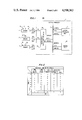
FIG. 1 is a block diagram of a computer system embodying the principles of the instant invention;
FIG. 2 illustrates a table utilized by the computer system set forth in FIG. 1 to vary the rate of time changes in polling sensors;
FIG. 3 illustrates a sensor buffer store layout of the central processor memory unit set forth in FIG. 1; and
FIGS. 4, 5, 6 and 7 illustrate a flow chart of the computer system polling sequence of the sensors set forth in FIG. 1.
DESCRIPTION OF THE INVENTION
1. Apparatus Description
Referring to the drawing, and more specifically to FIG. 1 of the drawing, computer system 100 set forth therein is intended for use in processing data that is received and stored in a number of sensors 1, 2, 3. Each sensor 1, 2, 3 is coupled by lines 10, 30 or data links 21, 31, or the combination thereof, with equipment such as for example, telephone switching equipment. The telephone switching equipment not shown in the drawing and which is not necessary for an understanding of the invention, generates varying amounts of data which is received over lines 10, 30 and the data links 21, 31 and stored in sensors 1, 2, 3. Sensors for use with telephone switching equipment have been described in the prior art and need not be described in detail for an understanding of the present invention. For example, an article by J. J. Kleber and W. B. Perkinson published in the July/August 1980 issue of Bell Laboratories Record, page 236, and entitled "No. 1A AMARC: At the Center of Billing Data Collection" describes a number of sensors and the functions thereof used to receive telephone switching system data that is subsequently processed to obtain customer billing information.
As set forth in FIG. 1, each sensor 1, 2, 3 is coupled by a data communication channel 14, 24, 34 respectively, with a central processor 4 arranged to process data generated by equipment coupled with sensors 1, 2, 3. Central processor 4 includes a stored program central processing unit 41 interconnected by a bus 43 through address, control, and data leads with a memory unit 42. In addition, central processor 41 and memory unit 42 are interconnected by bus 43 with asynchronous multiplexer interface unit 40 which is arranged to interface with and interconnect a number of data communications channels 14, 24, 34 with central processor 4. It is intended that central processor 4 and the component parts thereof such as asynchronous multiplexer interface unit 40, central processor 41, and memory unit 42 be conventional and well known. For example, a Terminals and Communications Handbook, copyright 1979, published by the Digital Equipment Corporation of Maynard, Mass., describes in Chapter 7, page 145, a conventional type of such a central processor. The present invention is not limited for use with the central processor set forth in the aforementioned handbook but may be utilized with other types of central processors as well.
Referring to FIG. 3 of the drawing, memory unit 42 includes a number of sensor buffer stores 420, 421, 422 each associated with a corresponding one of sensors 1, 2, 3. Thus, sensor buffer store 420 is associated with and is arranged to record the data received by sensor 1. Similarly, sensor buffer store 421 and sensor buffer store 422 are associated with and arranged to record respectively, data received by sensors 2 and 3. In the well known manner, address information appearing on bus 43 selects one of the sensor buffer stores 420, 421, 422 and control information enables memory unit 42 to store sensor data appearing on bus 43 within the addressed sensor buffer store 420, 421, 422. Recorded within each sensor buffer store is an adaptive time delay status 4200, 4210, 4220 controlling the interval of time between consecutive polls of the sensor associated with the sensor buffer store. Each recorded adaptive time delay status 4200, 4210, 4220 comprises a time delay state identifying a time interval between consecutive polls of the sensor associated with the sensor buffer store and a timer state identifying a period of time remaining to the next poll of the sensor,
2. General System Operation
In order to process the data received by sensors 1, 2, 3, FIG. 1, central processor 4 polls each sensor to collect and record the data accumulated by the sensor. The time interval between consecutive polls of a sensor is changed in accordance with the amount of data having been received by the sensor. If a sensor for example, sensor 1, begins to receive an increasing amount of data central processor 4 decreases the interval of time between consecutive polls and begins to poll sensor 1 at an increasing rate so that sensor 1 data does not overflow the limited sensor store capacity and thereby be lost. If on the other hand sensor 2 begins to receive a decreasing amount of data over data link 21, central processor 4 increases the interval of time between consecutive polls and begins to poll sensor 2 less often. When a sensor such as sensor 3 continues to receive a constant amount of data, central processor 4 maintains a constant interval of time between consecutive polls of sensor 3. Thus, central processor 4 by regulating the time interval and the rate of changing time intervals between consecutive sensor polls is able to optimize the data load offered central processor 4 and improve the efficiency of central processing unit 41 by minimizing time spent polling sensors.
In order to illustrate the operation of computer system 100, it is assumed that the time delay and timer states, FIG. 3, recorded in each sensor buffer store 420, 421, 422 of memory unit 42 are set to the value of 3 at 1.7, respectively. Furthermore, it is assumed that sensor 1 is being offered a large load of received data and is nearly full. Sensor 2 is being offered a small load of received data and is almost empty of data. Finally, sensor 3 is being offered an intermediate load of received data and is approximately half full of data.
Central processing unit 41 initiates the polling sequence by addressing memory unit 42 and reading the time delay state 3 and timer state 1.7 from addressed sensor 1 buffer store 420 into central processing unit 41. The read timer state is then decremented by an amount Z herein assumed to be 0.1. Since the decremented timer state is other than the null state, assumed for purpose of illustration to be 0.0, both the time delay state 3 and the decremented timer state 1.6 are transmitted from central processing unit 41 to memory unit 42 and stored in addressed sensor buffer store 420. Similarly, central processing unit 41 reads the time delay state 3 and timer state 1.7 recorded in sensor buffer stores 421, 422 of memory unit 42, decrements the read timer state by 0.1 and stores both time delay state 3 and decremented timer state 1.6 in sensor buffer store 421 and 422.
Central processing unit 42 continues during the polling sequence to sequentially read the time delay status states 4200, 4210, 4220 of each sensor buffer store 420, 421, 422 and decrement the timer states identifying the time remaining to the next poll of the sensor. When the timer state read from sensor buffer store 420 is decremented to the null state, central processing unit 42 responds by addressing asynchronous multiplexer interface unit 40, FIG. 1, to assume a transmit state thereby enabling central processor 4 to transmit a poll command over data communication channel 14 to sensor 1. Asychronous multiplexer interface unit 40 is then addressed and controlled to receive data and sensor 1 then transmits the accumulated received data over data communication channel 14 to central processor 4.
The sensor 1 data collected by central processor 4 and recorded in sensor store buffer 420, FIG. 3, is counted by central processing unit 41 and compared with the capacity of sensor buffer store 420. Since it was assumed that sensor 1 was nearly full of data, central processing unit 41 determines from the proportional relationship of received sensor 1 data with the capacity of sensor buffer store 420 that sensor buffer store 420 is greater than Y % full and the rate of polling sensor 1 should be increased. Accordingly, central processing unit 41 enters the Adaptive Time Delay Status Table set forth in FIG. 2 at the row identified by the read time delay state 3 and determines that the time delay state for the nearly full sensor 1 should be decreased from 3 to 2. Central processing unit 41 further determines from the table of FIG. 2 that a timer state of 0.9 is associated with time delay state 2 and then sets the time delay and timer states respectively to 2 and 0.9 and transmits the set time delay and timer states to memory 42 to be stored in sensor buffer store 420.
As the poll sequence continues, sensor buffer store 421 time delay and timer states are read into central processing unit 41 and the timer state decremented by 0.1. When the read timer state is decremented to the null state, sensor 2 is polled and the received data collected and recorded by central processor 4. The collected and recorded data is compared in a proportional relationship with the data capacity of sensor buffer store 421. Since it was assumed that sensor 2 was nearly empty then sensor buffer store 421 is less than X % full and the rate of polling sensor 2 should be decreased. Accordingly, central processing unit 41 enters the Adaptive Time Delay Status Table of FIG. 2 at the row identified by the read time delay state 3 and determines that the time delay state for the nearly empty sensor 2 should be increased from 3 to 4. Central processing unit 41 then sets the time delay state for sensor 2 to 4 and the timer state to 2.7 and transmits the set time delay and timer states to memory 42 to be stored in sensor buffer store 421. When the read and decremented timer state of sensor buffer store 422 is in the null state, the proportional relationship of data collected and recorded from polled sensor 3 with the data capacity of sensor buffer store 422 indicates that sensor 3 has only partially filled with data during the time interval since the last poll. Central processing unit 41 then enters the Adaptive Time Delay Status Table at row 3 identified by the read time delay state 3 and determines that the time delay state for sensor 3 should remain at the value of 3. Accordingly, the time delay and timer states are set to 3 and 1.7 respectively, transmitted to memory unit 42 and stored as time delay status 4220 in sensor buffer store 422, FIG. 3.
If the data received by sensor 1 continues to increase and sensor buffer store 420 is nearly full every time sensor 1 is polled then the time delay and timer states, currently set to 2 and 0.9, respectively, are decreased during the next consecutive poll to 1 and 0.4 as set forth in the Adaptive Time Delay Status Table of FIG. 2. When the timer state recorded in sensor buffer store 420 is decremented from 0.4 to 0.0 and polled sensor 1 is still nearly full of received data then the time delay and timer states are set to 0 and 0.0 respectively, and stored in sensor buffer store 420 so that time delay status 4200 may control central processor 4 to poll sensor 1 each time the recorded time delay status 4200 is read into central processing unit 41. Central processor 4 responds to the increasing amount of data received by sensor 1 by decreasing the rate of the time interval between consecutive polls so as to increase the number of times that sensor 1 is polled. Thus, the time delay state is decreased from the assumed initial value of 3 to 2, 1 and then 0. In addition, the timer state 1.7 originally corresponding to the time delay state 3 is changed by a decreasing rate of change of 0.8, 0.5 and 0.4 from 1.7 to 0.9 then to 0.4 and finally to 0. The time interval between consecutive polls of sensor 1 has been decreased to thereby increase the polling of sensor 1 and guard against sensor 1 from overflowing with data.
In contrast to sensor 1, the data received by sensor 2 was assumed to be decreasing such that sensor 2 was nearly empty of received data during each poll. Accordingly, the time delay and timer states recorded in sensor buffer store 421 and currently set to 4 and 2.7 respectively, are increased during succeeding polls of sensor 2 to the time delay states 5, 6, 7 and the corresponding timer states of 4.2, 6.2 and 9.0. Central processor 4 is thereby controlled by time delay status 4210 recorded in sensor buffer store 421 to increase the rate of change of time by the values 1.5, 2.0 and 2.8 in delaying subsequent polls of sensor 2.
Since sensor 3 has been assumed to receive a constant amount of data, the time delay and timer states recorded in the partially full sensor buffer store 422 continue to be reset during each poll of sensor 3 to the values of 3 and 1.7 respectively. Thus, sensor 3 is polled with a constant interval of time between consecutive polls.
As the amount of data received by sensors 1, 2, 3 varies, central processor 4 dynamically regulates the time delay status 4200, 4210, 4220 recorded in sensor buffer stores 420, 421, 422 to control the interval of time between consecutive polls and optimize the data load offered by sensors 1, 2, 3 to central processor 4.
3. Detailed System Operation
Referring now to FIG. 4 of the drawing, central processing unit 4 initiates sensor poll sequence 5 by entering a poll sequence at step 50. A time delay status comprising a time delay state and a timer state is read at step 51 from a sensor buffer store of memory 42 over bus 43 into central processing unit 41. Central processing unit 41 then decrements the read timer state identifying the time remaining to the next poll of the sensor at step 52 by subtracting the value of Z therefrom where Z is a value of time determined by the characteristics of computer system 100. If the decremented timer state is other than the null state, central processing unit 41, steps 53, 530, and 531, transmits the decremented timer state over bus 43 and stores the value thereof in the sensor buffer store. Central processing unit 41 then continues, steps 591, 5910, FIG. 7, poll sequence 5, by reading the time delay and timer states, step 51, FIG. 4, from another sensor buffer. After all sensor buffer store time delay and timer states have been read central processing unit 41 then exits poll sequence 5 at steps 591 and 592 to perform other system functions.
If the decremented timer state, step 53, is determined to be in the null state, central processor 4 will poll the sensor associated with sensor buffer store from which the time delay and timer states were read in step 54. In initiating the step 54 of transmitting a poll command to the sensor, central processing unit 41 addresses and controls asynchronous multiplexer interface unit 40, step 540, over bus 43 to enter the transmit state. Central processor 4, step 541, then transmits a poll command from asynchronous multiplexer interface unit 40 over the appropriate one of data communication channels 14, 24, 34 to the polled sensor. At step 542, FIG. 5, central processing unit 41 addresses and controls asynchronous multiplexer interface unit 40 over bus 43 to enter a receive state to collect data over the appropriate data communication channel from the polled sensor.
Central processing unit 41 in recording the data collected from the polled sensor, zeros a register, step 550, assigned to accumulate a byte count of the sensor data collected and recorded, step 55, in the memory unit sensor buffer store associated with the polled sensor. Each byte of collected sensor data, step 551, is removed from asynchronous multiplexer interface unit 40 over bus 43 and recorded in the associated sensor buffer store. As each byte of polled sensor data is recorded in the appropriate sensor buffer store the central processing unit sensor buffer store byte count register, step 552, is increased by 1. The counting is continued via steps 551, 552, 553 and path 5530 until an end of block signal is detected at step 553 thereby indicating that all of the polled sensor data has been collected and recorded in the associated sensor buffer store of memory unit 42.
When the end of block signal has been detected, central processing unit 41, FIG. 6, step 560, zeros Adaptive Time Delay Status Table i and j registers prior to setting the time delay status, step 57, to control subsequent polling of the sensor. If the central processing unit 41 sensor buffer store byte count register representing the amount of data received by the polled sensor is greater than Y % full, step 561, then the central processing unit 41 sets Adaptive Time Delay Status Table j register to 4, step 570. The values of X % and Y % are statistically chosen with respect to capacity of the sensor and the data processing capability of central processor 4. Thus, central processor 4 processes the received sensor data most efficiently when each block of recorded data contains a number of bytes of data in the range greater than or equal to X % full but less than or equal to Y % full. Typically, X % and Y % may have the values of 80 and 90 respectively. When the number of bytes of received sensor data is greater than the value of Y % then the sensor must be polled more often to prevent loss of data. If the number of bytes of received sensor data is less than the value of X %, central processor 4 would be operating less efficiently in that more processor time is required to poll the sensor to receive small blocks of data and less processor time is available to do other tasks. Thus, the sensor should be polled less often. Since the most efficient operation of central processor 4 occurs when the received sensor data is in the range between X %, and Y % central processor 4 effects changes of the time interval in polling sensors to maintain the sensor data recorded in each sensor buffer store in the range between X % and Y % so as to optimize the data load offered central processor 4.
If the central processing unit 41 sensor buffer store byte count register is equal to or less than Y % full but greater than or equal to X % full, step 562, then the Adaptive Time Delay Status Table j register is set to 3, step 571. Should the sensor buffer store byte count register indicate that the polled sensor is less than X % full, the central processing unit 41, step 572, sets the Adaptive Time Delay Status Table j register to 2.
Once the Adaptive Time Delay Status Table j register has been set, steps 570, 571, 572, central processing unit 41 then sets the Adaptive Time Delay Status Table i register, step 573, to the value of the time delay state previously read from the sensor buffer store associated with the polled sensor. Central processing unit 41, FIG. 7 step 574, reads the Adaptive Time Delay Status Table of FIG. 2 at the row i that corresponds to the read time delay state and at the column j that corresponds to the amount of data that was collected and recorded from the polled sensor. If the sensor buffer store was full of data such that the Adaptive Time Delay Status Table j register, step 574, was set to 4 then the present time delay state is decreased by 1 so as to increase the polling rate of the sensor and thereby prevent loss of data. It is to be understood that the Adaptive Time Delay Status Table can be structured such that the change of the time delay state can be more than 1 if the characteristics of the sensor and data traffic so warrant.
When the Adaptive Time Delay Status Table j register, step 571, is set to 3, the present time delay state is retained to maintain the sensor data in the range between X % and Y %. Should the Adaptive Time Delay Status Table j register, step 572, be set to 2, then the present time delay state is increased by 1 to increase the time between successive polls of the sensor.
The time delay state, step 575, is set to the value read from the Adaptive Time Delay Status Table at the row and column defined by the Adaptive Time Delay Status i and j registers and the read timer state is set, step 576, to the table value of the row defined by the set time delay state and column 1. Central processing unit 41 then transmits, step 580, the set time delay and timer states over bus 43 to memory unit 42 and stores the values thereof, step 581, in the sensor buffer store associated with the polled sensor.
Poll sequence 5 then exits the poll sequence, step 591, or reads the time delay and timer states, path 5910, from the next sensor buffer store, step 51, into central processing unit 41.
SUMMARY
It is obvious from the foregoing that the facility, economy, and efficiency of computer systems may be substantially enhanced by the provision of a computer system arranged to optimize the data load offered by sensors to a central processor. It is further obvious from the foregoing that the aforesaid computer system arranged to dynamically vary the time of polling each sensor of a plurality of sensors to smooth the data load offered by the sensors to a central processor improves the efficiency of the central processor by optimizing the central processor polling time and allowing more data processing time.
While the apparatus and method of the invention has been disclosed in a computer system for use with telephone switching equipment, it is to be understood that such an embodiment is intended to be illustrative of the principles of the invention in that numerous other arrangements may be devised with those skilled in the art without departing from the spirit and scope of the invention.

Claims (13)

What is claimed is:
1. A method of polling sensors (1, 2, 3) receiving data intended for processing by a central processor (4) coupled with the sensors comprising the step of
polling (5) the sensors to collect and record the sensor data in sensor buffer stores (421, 422, 433) each associated with a sensor and each located in a memory unit (42) of the central processor
characterized in that
said polling step comprises the steps of
recording (51, 52, 53, 54, 58) in each sensor buffer store an adaptive time delay status controlling an interval of time between consecutive polls of the sensor associated with the sensor buffer store, and
dynamically regulating (55, 56, 57) said recorded time delay status in accordance with a proportional relationship of the received sensor data with the data capacity of the sensor buffer store associated with the sensor to optimize the data load offered by the sensors to the central processor.
2. The sensor polling method of claim 1
characterized in that
said recording step further comprises the step of
reading (51) a time delay state identifying a time interval between consecutive polls of the sensor and a timer state identifying a period of time remaining to the next poll of the sensor from the associated sensor buffer store of the memory unit into a processing unit of the central processor.
3. The sensor polling method of claim 2
characterized in that
said recording step further comprises the step of
decrementing (52, 53, 531) said read timer state and storing said decremented timer state in the associated sensor buffer store when said decremented timer state is other than a null state.
4. The sensor polling method of claim 3
characterized in that
said recording step further comprises the step of
transmitting (54) a poll command to the sensor in response to a null state registered in said decremented timer state.
5. The sensor polling method of claim 4
characterized in that
said regulating step comprises the steps of
counting (55, 56) data collected and recorded in the sensor buffer store associated with the sensor and comparing said data count with a data capacity of the sensor buffer store, and
setting (57) the time delay and timer states in accordance with proportional relationships of said counted sensor data with said sensor buffer store data capacity to regulate the interval of time between successive polls of the sensor.
6. The sensor polling method of claim 5
characterized in that
said recording step further comprises the step of
transmitting (58) said set time delay and timer states from the processing unit to the memory unit and storing said set time delay and timer states in the sensor buffer store associated with the polled sensor.
7. A method of polling sensors (1, 2, 3) receiving data intended for processing by a central processor (4) coupled with the sensors comprising the step of
polling (5) the sensors to collect and record the sensor data in sensor buffer stores (421, 422, 423) each associated with a sensor and each located in a memory unit (42) of the central processor
characterized in that
said polling step comprises the steps of
reading (51) a time delay state identifying a time interval between consecutive polls of a sensor and a timer state identifying a period of time remaining to the next poll of the sensor from a sensor buffer store associated with the sensor of the memory unit into a processing unit of the central processor,
decrementing (52, 53, 54) said read timer state and transmitting a poll command to the sensor in response to a null state registered in said decremented timer state,
setting (55, 56, 57) said read time delay and timer states in accordance with proportional relationships of the polled sensor data with the data capacity of the sensor buffer store to regulate and optimize the data load offered by the sensors to the central processor, and
transmitting (58) said set time delay and timer states from the processing unit and storing said set time delay and timer states in the sensor buffer store of the memory unit.
8. The sensor polling method of claim 7
characterized in that
said setting step comprises the steps of
counting (55) bytes of sensor data collected and recorded in the sensor buffer store of the polled sensor,
determining (56) a proportional relationship of said counted bytes of sensor data with the data byte capacity of the sensor buffer store,
incrementing (572, 573, 574, 575, 576) said read time delay state when said determined proportional relationship is less than a first defined value and setting said read timer state to increase the period of time to the next poll of the sensor,
decrementing (570, 573, 574, 575, 576) said read time delay state when said determined proportional relationship is greater than a second defined value and setting said read timer state to decrease the period of time to the next poll of the sensor, and
retaining (571, 573, 574, 575, 576) said read timer delay state when said determined proportional relationship is greater than or equal to said first defined value and less than or equal to said second defined value and setting said read timer state to the value set in the previous poll of the sensor.
9. A method of polling sensors (1, 2, 3) receiving data intended for processing by a central processor (4) coupled with the sensors comprising the step of
polling (5) the sensors to collect and record the sensor data in sensor buffer stores (421, 422, 423) each associated with a sensor and each located in a memory unit (42) of the central processor
characterized in that
said polling step comprises the steps of
reading (51) a time delay state identifying an interval of time between consecutive polls of a sensor and a timer state identifying an interval of time remaining to the next poll of the sensor from a sensor buffer store associated with the sensor of the memory unit into a processing unit of the central processor,
decrementing (52, 53, 531) said read timer state and storing said decremented timer state in the sensor buffer store when said decremented timer state is other than a null state,
transmitting (54) a poll command to the sensor in response to a null state registered in said decremented timer state,
counting (55) bytes of sensor data collected and recorded in the sensor buffer store in response to said transmitted poll command,
incrementing (55, 572, 573, 574, 575, 576) said read time delay state when a proportional relationship of said counted bytes of sensor data with the data byte capacity of the sensor buffer store is less than a first defined value and setting said timer state to increase the period of time to the next poll of the sensor,
decrementing (56, 570, 573, 574, 575, 576) said read time delay state when the proportional relationship of said counted bytes of sensor data with the data byte capacity of the sensor buffer store is greater than a second defined value and setting said timer state to decrease the period of time to the next poll of the sensor,
retaining (56, 571, 573, 574, 575, 576) said read time delay state when the proportional relationship of said counted bytes of sensor data with the data byte capacity of the sensor buffer store is greater than or equal to said first defined value and less than or equal to said second defined value and setting said timer state to the value set in the previous poll of the sensor, and
transmitting (58) said set time delay and timer states from said processing unit to said memory unit and storing said set time delay and timer states in the sensor buffer store.
10. A method of polling a plurality of sensors (1, 2, 3) each coupled with a central processor intended for processing data comprising the step of
polling the sensors to collect and record data received by each sensor in a sensor buffer store of a memory unit of the central processor
characterized in that
said polling step comprises the steps of
recording (51, 52, 53, 54, 58) in the sensor buffer store an adaptive time delay status controlling a time interval between polling the sensors,
incrementing (55, 56, 572, 573, 574, 575, 576) said recorded time delay status in response to decreasing amounts of data received by a polled one of the sensors to increase the time interval between subsequent polls of the sensor,
decreasing (55, 56, 570, 573, 574, 575, 576) said recorded time delay status in response to increasing amounts of data received by a polled one of the sensors to decrease the time interval between subsequent polls of the sensor, and
maintaining (55, 56, 571, 573, 574, 575, 576) said recorded time delay status in response to a constant amount of data received by a polled one of the sensors to maintain a constant interval of time between consecutive polls of the sensor.
11. A computer system (100) for processing data received by a plurality of sensors (1, 2, 3) comprising
apparatus (4) coupled with the sensors for polling the sensors to collect and record the data accumulated by each sensor
characterized in that
said polling apparatus comprises
means (42) for recording an adaptive time delay status individual to each sensor controlling an interval of time between consecutive polls of the sensor, and
means (41) responsive to changes in amounts of data received by the sensors for dynamically regulating said adaptive time delay status in said recording means to vary a rate of time changes in polling the sensors and optimize the data load offered by the sensors to the computer system.
12. The computer system of claim 11
characterized in that
said recording means comprises
a memory unit (42) having a plurality of sensor buffer stores (420, 421, 422) each associated with one of the sensors to record sensor data and each recording a time delay state identifying the time interval between consecutive polls of the sensor and a timer state identifying a period of time remaining to the next sensor poll.
13. The computer system in claim 12
characterized in that
said regulating means comprises
a central processor (41) decrementing said recorded timer state and polling each sensor in response to a null of the timer state for setting both said time delay and timer states recorded in a sensor buffer store associated with a polled sensor in accordance with proportional relationships of the polled sensor data with the data capacity of the sensor buffer store to vary the rate of changing an interval of time in polling the sensor.
US06/511,742 1983-07-07 1983-07-07 Adaptive delayed polling of sensors Expired - Lifetime US4598363A (en)

Priority Applications (1)

Application Number Priority Date Filing Date Title
US06/511,742 US4598363A (en) 1983-07-07 1983-07-07 Adaptive delayed polling of sensors

Applications Claiming Priority (1)

Application Number Priority Date Filing Date Title
US06/511,742 US4598363A (en) 1983-07-07 1983-07-07 Adaptive delayed polling of sensors

Publications (1)

Publication Number Publication Date
US4598363A true US4598363A (en) 1986-07-01

Family

ID=24036238

Family Applications (1)

Application Number Title Priority Date Filing Date
US06/511,742 Expired - Lifetime US4598363A (en) 1983-07-07 1983-07-07 Adaptive delayed polling of sensors

Country Status (1)

Country Link
US (1) US4598363A (en)

Cited By (38)

* Cited by examiner, † Cited by third party
Publication number Priority date Publication date Assignee Title
US4682296A (en) * 1983-10-14 1987-07-21 United Kingdom Atomic Energy Authority Ultrasonic imaging
US4754399A (en) * 1983-12-28 1988-06-28 Hitachi, Ltd. Data transfer control system for controlling data transfer between a buffer memory and input/output devices
US5130983A (en) * 1990-03-27 1992-07-14 Heffner Iii Horace W Method of polling to determine service needs and the like
US5201053A (en) * 1990-08-31 1993-04-06 International Business Machines Corporation Dynamic polling of devices for nonsynchronous channel connection
US5247617A (en) * 1991-02-26 1993-09-21 Digi International, Inc. Method for supplying data to a buffered uart
US5319785A (en) * 1991-06-28 1994-06-07 Digital Equipment Corporation Polling of I/O device status comparison performed in the polled I/O device
US5396598A (en) * 1993-05-07 1995-03-07 The United States Of America As Represented By The Secretary Of The Army Event-driven signal processor interface having multiple paralleled microprocessor-controlled data processors for accurately receiving, timing and serially retransmitting asynchronous data with quickly variable data rates
EP0652523A1 (en) * 1993-11-10 1995-05-10 Nec Corporation Remote monitoring system
EP0689144A1 (en) * 1994-06-20 1995-12-27 International Business Machines Corporation Adaptive polling system and method
US5488693A (en) * 1992-06-24 1996-01-30 At&T Corp. Protocol with control bits and bytes for controlling the order of communications between a master processor and plural slave processors
US5539882A (en) * 1992-12-16 1996-07-23 International Business Machines Corporation Method and system for an efficient multiple access polling protocol for interactive communication
US5594871A (en) * 1991-04-25 1997-01-14 Canon Kabushiki Kaisha Data communication method and data communication system using data communication apparatus therein
EP0777357A3 (en) * 1995-11-28 1997-10-22 Ncr Int Inc Network management system with improved node discovery and monitoring
US5758189A (en) * 1994-06-23 1998-05-26 Fujitsu Limited System for changing period to examine external storage unit for storage medium being loaded based on state of use of input device
US6173323B1 (en) * 1997-12-24 2001-01-09 Lucent Technologies Inc. Adaptive polling rate algorithm for SNMP-based network monitoring
US6182165B1 (en) * 1998-06-01 2001-01-30 Advanced Micro Devices, Inc. Staggered polling of buffer descriptors in a buffer descriptor ring direct memory access system
US6449663B1 (en) * 1998-07-08 2002-09-10 International Business Machines Corporation Method and apparatus for adjusting an interval of polling a network printer based on changes in working status of the network printer
US20020184555A1 (en) * 2001-04-23 2002-12-05 Wong Joseph D. Systems and methods for providing automated diagnostic services for a cluster computer system
US6640268B1 (en) * 1998-08-28 2003-10-28 Intel Corporation Dynamic polling mechanism for wireless devices
US20040213589A1 (en) * 2003-04-22 2004-10-28 Barbera Joseph D. Efficient sensing system
US20040236880A1 (en) * 2003-05-19 2004-11-25 Emulex Corporation Dynamically self-adjusting polling mechanism
US20050210128A1 (en) * 2004-03-16 2005-09-22 Cannon David M Apparatus, system, and method for adaptive polling of monitored systems
US20050272423A1 (en) * 2004-06-02 2005-12-08 Stephens Adrian P Adaptive polling of wireless devices
US20090006644A1 (en) * 2007-06-29 2009-01-01 Scott Forstall Port discovery and message delivery in a portable electronic device
US20090006570A1 (en) * 2007-06-29 2009-01-01 Scott Forstall Email fetching system and method in a portable electronic device
US20100318693A1 (en) * 2009-06-11 2010-12-16 Espig Michael J Delegating A Poll Operation To Another Device
US8024499B1 (en) * 2008-01-17 2011-09-20 Juniper Networks, Inc. Systems and methods for automated sensor polling
US8631208B2 (en) 2009-01-27 2014-01-14 Intel Corporation Providing address range coherency capability to a device
US8866469B2 (en) 2011-03-12 2014-10-21 Altas Polar Company Limited Electric field monitoring system and method
US8914551B2 (en) 2013-04-09 2014-12-16 Analog Devices, Inc. Sensor polling unit for microprocessor integration
US9092132B2 (en) 2011-01-24 2015-07-28 Apple Inc. Device, method, and graphical user interface with a dynamic gesture disambiguation threshold
US9128614B2 (en) 2010-11-05 2015-09-08 Apple Inc. Device, method, and graphical user interface for manipulating soft keyboards
US9141285B2 (en) 2010-11-05 2015-09-22 Apple Inc. Device, method, and graphical user interface for manipulating soft keyboards
US9436381B2 (en) 2011-01-24 2016-09-06 Apple Inc. Device, method, and graphical user interface for navigating and annotating an electronic document
US9442654B2 (en) 2010-01-06 2016-09-13 Apple Inc. Apparatus and method for conditionally enabling or disabling soft buttons
US9680635B2 (en) 2014-02-12 2017-06-13 Infineon Technologies Ag Sensor subassembly and method for sending a data signal
US10243724B2 (en) 2014-02-12 2019-03-26 Infineon Technologies Ag Sensor subassembly and method for sending a data signal
US20210367858A1 (en) * 2014-02-24 2021-11-25 Huawei Technologies Co., Ltd. Information Processing Method in M2M and Apparatus

Citations (9)

* Cited by examiner, † Cited by third party
Publication number Priority date Publication date Assignee Title
US4040026A (en) * 1974-05-08 1977-08-02 Francois Gernelle Channel for exchanging information between a computer and rapid peripheral units
US4083229A (en) * 1976-09-28 1978-04-11 Plaunt & Anderson Company, Inc. Method and apparatus for detecting and locating fluid leaks
US4117278A (en) * 1977-09-19 1978-09-26 Bell Telephone Laboratories, Incorporated Service observing terminal
US4125870A (en) * 1975-10-15 1978-11-14 Tokyo Shibaura Electric Co., Ltd. Information transfer control system
US4236225A (en) * 1977-12-12 1980-11-25 U.S. Philips Corporation Data buffer memory of the first-in, first-out type, having a variable input and a fixed output
US4432481A (en) * 1982-06-14 1984-02-21 Owens-Illinois, Inc. Splice-in-register control
US4468809A (en) * 1981-12-23 1984-08-28 Ncr Corporation Multiple font OCR reader
US4479194A (en) * 1982-08-10 1984-10-23 Computer Election Systems System and method for reading marks on a document
US4514621A (en) * 1977-02-21 1985-04-30 Australasian Training Aids (Pty.) Limited Firing range

Patent Citations (11)

* Cited by examiner, † Cited by third party
Publication number Priority date Publication date Assignee Title
US4040026A (en) * 1974-05-08 1977-08-02 Francois Gernelle Channel for exchanging information between a computer and rapid peripheral units
US4125870A (en) * 1975-10-15 1978-11-14 Tokyo Shibaura Electric Co., Ltd. Information transfer control system
US4083229A (en) * 1976-09-28 1978-04-11 Plaunt & Anderson Company, Inc. Method and apparatus for detecting and locating fluid leaks
US4083229B1 (en) * 1976-09-28 1983-02-01
US4083229B2 (en) * 1976-09-28 1984-09-11 Method and apparatus for detecting and locating fluid leaks
US4514621A (en) * 1977-02-21 1985-04-30 Australasian Training Aids (Pty.) Limited Firing range
US4117278A (en) * 1977-09-19 1978-09-26 Bell Telephone Laboratories, Incorporated Service observing terminal
US4236225A (en) * 1977-12-12 1980-11-25 U.S. Philips Corporation Data buffer memory of the first-in, first-out type, having a variable input and a fixed output
US4468809A (en) * 1981-12-23 1984-08-28 Ncr Corporation Multiple font OCR reader
US4432481A (en) * 1982-06-14 1984-02-21 Owens-Illinois, Inc. Splice-in-register control
US4479194A (en) * 1982-08-10 1984-10-23 Computer Election Systems System and method for reading marks on a document

Non-Patent Citations (2)

* Cited by examiner, † Cited by third party
Title
J. J. Kleber et al, No. 1A AMARC at the Center of Billing Data Collection, Bell Labs. Record (Jul./Aug. 1980), pp. 236 243. *
J. J. Kleber et al, No. 1A AMARC at the Center of Billing Data Collection, Bell Labs. Record (Jul./Aug. 1980), pp. 236-243.

Cited By (60)

* Cited by examiner, † Cited by third party
Publication number Priority date Publication date Assignee Title
US4682296A (en) * 1983-10-14 1987-07-21 United Kingdom Atomic Energy Authority Ultrasonic imaging
US4754399A (en) * 1983-12-28 1988-06-28 Hitachi, Ltd. Data transfer control system for controlling data transfer between a buffer memory and input/output devices
US5130983A (en) * 1990-03-27 1992-07-14 Heffner Iii Horace W Method of polling to determine service needs and the like
US5201053A (en) * 1990-08-31 1993-04-06 International Business Machines Corporation Dynamic polling of devices for nonsynchronous channel connection
US5247617A (en) * 1991-02-26 1993-09-21 Digi International, Inc. Method for supplying data to a buffered uart
US5594871A (en) * 1991-04-25 1997-01-14 Canon Kabushiki Kaisha Data communication method and data communication system using data communication apparatus therein
US5319785A (en) * 1991-06-28 1994-06-07 Digital Equipment Corporation Polling of I/O device status comparison performed in the polled I/O device
US5488693A (en) * 1992-06-24 1996-01-30 At&T Corp. Protocol with control bits and bytes for controlling the order of communications between a master processor and plural slave processors
US5889963A (en) * 1992-12-16 1999-03-30 International Business Machines Corporation Method and system for an efficient multiple access polling protocol for interactive communication
US5539882A (en) * 1992-12-16 1996-07-23 International Business Machines Corporation Method and system for an efficient multiple access polling protocol for interactive communication
US5396598A (en) * 1993-05-07 1995-03-07 The United States Of America As Represented By The Secretary Of The Army Event-driven signal processor interface having multiple paralleled microprocessor-controlled data processors for accurately receiving, timing and serially retransmitting asynchronous data with quickly variable data rates
US5586056A (en) * 1993-11-10 1996-12-17 Nec Corporation Remote monitoring system using a polling level table and a monitored station number table
EP0652523A1 (en) * 1993-11-10 1995-05-10 Nec Corporation Remote monitoring system
US5566351A (en) * 1994-06-20 1996-10-15 International Business Machines Corporation Adaptive polling system by generating sequence of polling signals whose magnitudes are functionally related to the occurrence of the busy signal
EP0689144A1 (en) * 1994-06-20 1995-12-27 International Business Machines Corporation Adaptive polling system and method
US5758189A (en) * 1994-06-23 1998-05-26 Fujitsu Limited System for changing period to examine external storage unit for storage medium being loaded based on state of use of input device
EP0777357A3 (en) * 1995-11-28 1997-10-22 Ncr Int Inc Network management system with improved node discovery and monitoring
US6173323B1 (en) * 1997-12-24 2001-01-09 Lucent Technologies Inc. Adaptive polling rate algorithm for SNMP-based network monitoring
US6182165B1 (en) * 1998-06-01 2001-01-30 Advanced Micro Devices, Inc. Staggered polling of buffer descriptors in a buffer descriptor ring direct memory access system
US6449663B1 (en) * 1998-07-08 2002-09-10 International Business Machines Corporation Method and apparatus for adjusting an interval of polling a network printer based on changes in working status of the network printer
US6640268B1 (en) * 1998-08-28 2003-10-28 Intel Corporation Dynamic polling mechanism for wireless devices
US6895534B2 (en) * 2001-04-23 2005-05-17 Hewlett-Packard Development Company, L.P. Systems and methods for providing automated diagnostic services for a cluster computer system
US20020184555A1 (en) * 2001-04-23 2002-12-05 Wong Joseph D. Systems and methods for providing automated diagnostic services for a cluster computer system
US20040213589A1 (en) * 2003-04-22 2004-10-28 Barbera Joseph D. Efficient sensing system
US7596328B2 (en) * 2003-04-22 2009-09-29 Hewlett-Packard Development Company, L.P. Efficient sensing system
US20040236880A1 (en) * 2003-05-19 2004-11-25 Emulex Corporation Dynamically self-adjusting polling mechanism
WO2004104730A2 (en) * 2003-05-19 2004-12-02 Emulex Design & Manufacturing Corporation Dynamically self-adjusting polling mechanism
WO2004104730A3 (en) * 2003-05-19 2005-04-28 Emulex Design & Mfg Corp Dynamically self-adjusting polling mechanism
US6931460B2 (en) * 2003-05-19 2005-08-16 Emulex Design & Manufacturing Corporation Dynamically self-adjusting polling mechanism
US20050210128A1 (en) * 2004-03-16 2005-09-22 Cannon David M Apparatus, system, and method for adaptive polling of monitored systems
US7631076B2 (en) 2004-03-16 2009-12-08 International Business Machines Corporation Apparatus, system, and method for adaptive polling of monitored systems
WO2005122488A1 (en) * 2004-06-02 2005-12-22 Intel Corporation Adaptive polling of wireless devices
US20050272423A1 (en) * 2004-06-02 2005-12-08 Stephens Adrian P Adaptive polling of wireless devices
CN101120538B (en) * 2004-06-02 2014-11-26 英特尔公司 Adaptive polling method, apparatus and system of wireless devices
US8121595B2 (en) * 2004-06-02 2012-02-21 Intel Corporation Adaptive polling of wireless devices
US8577971B2 (en) * 2007-06-29 2013-11-05 Apple Inc. Email fetching system and method in a portable electronic device
US20090006644A1 (en) * 2007-06-29 2009-01-01 Scott Forstall Port discovery and message delivery in a portable electronic device
US20090006570A1 (en) * 2007-06-29 2009-01-01 Scott Forstall Email fetching system and method in a portable electronic device
US8539093B2 (en) 2007-06-29 2013-09-17 Apple Inc. Port discovery and message delivery in a portable electronic device
US8024499B1 (en) * 2008-01-17 2011-09-20 Juniper Networks, Inc. Systems and methods for automated sensor polling
US8266343B2 (en) 2008-01-17 2012-09-11 Juniper Networks, Inc. Systems and methods for automated sensor polling
US8631208B2 (en) 2009-01-27 2014-01-14 Intel Corporation Providing address range coherency capability to a device
US8364862B2 (en) * 2009-06-11 2013-01-29 Intel Corporation Delegating a poll operation to another device
US8762599B2 (en) * 2009-06-11 2014-06-24 Intel Corporation Delegating a poll operation to another device
US20130138843A1 (en) * 2009-06-11 2013-05-30 Michael J. Espig Delegating a poll operation to another device
US20100318693A1 (en) * 2009-06-11 2010-12-16 Espig Michael J Delegating A Poll Operation To Another Device
US9442654B2 (en) 2010-01-06 2016-09-13 Apple Inc. Apparatus and method for conditionally enabling or disabling soft buttons
US9141285B2 (en) 2010-11-05 2015-09-22 Apple Inc. Device, method, and graphical user interface for manipulating soft keyboards
US9146673B2 (en) 2010-11-05 2015-09-29 Apple Inc. Device, method, and graphical user interface for manipulating soft keyboards
US9128614B2 (en) 2010-11-05 2015-09-08 Apple Inc. Device, method, and graphical user interface for manipulating soft keyboards
US10042549B2 (en) 2011-01-24 2018-08-07 Apple Inc. Device, method, and graphical user interface with a dynamic gesture disambiguation threshold
US9092132B2 (en) 2011-01-24 2015-07-28 Apple Inc. Device, method, and graphical user interface with a dynamic gesture disambiguation threshold
US9436381B2 (en) 2011-01-24 2016-09-06 Apple Inc. Device, method, and graphical user interface for navigating and annotating an electronic document
US10365819B2 (en) 2011-01-24 2019-07-30 Apple Inc. Device, method, and graphical user interface for displaying a character input user interface
US8866469B2 (en) 2011-03-12 2014-10-21 Altas Polar Company Limited Electric field monitoring system and method
US8914551B2 (en) 2013-04-09 2014-12-16 Analog Devices, Inc. Sensor polling unit for microprocessor integration
US9680635B2 (en) 2014-02-12 2017-06-13 Infineon Technologies Ag Sensor subassembly and method for sending a data signal
US10243724B2 (en) 2014-02-12 2019-03-26 Infineon Technologies Ag Sensor subassembly and method for sending a data signal
US20210367858A1 (en) * 2014-02-24 2021-11-25 Huawei Technologies Co., Ltd. Information Processing Method in M2M and Apparatus
US11799735B2 (en) * 2014-02-24 2023-10-24 Huawei Cloud Computing Technologies Co., Ltd. Information processing method in M2M and apparatus

Similar Documents

Publication Publication Date Title
US4598363A (en) Adaptive delayed polling of sensors
KR0129000B1 (en) Advanced data communication apparatus and data character recognition and transfer method
US5542076A (en) Method and apparatus for adaptive interrupt servicing in data processing system
US4654632A (en) Analog-to-digital converter
GB2101374A (en) Interface circuit
US5414816A (en) Data transfer apparatus having means for controlling the difference in speed between data input/output ports and memory access
US5151999A (en) Serial communications controller for transfer of successive data frames with storage of supplemental data and word counts
US4497979A (en) Method for processing essential lines in a communication system
KR0155368B1 (en) Ram based event counter method and apparatus
US4918597A (en) Adaptive interface for transferring segmented message between device and microcomputer on line division multiplexed bus
US4805170A (en) Data communication network
CN1082755C (en) A T M cell froming device
JPH0744567B2 (en) Communication interface device
JPS5926158B2 (en) Overload control method
JP2563821B2 (en) Packet transmitter
JP2924264B2 (en) ATM switch
JP2687324B2 (en) Reception buffer control method
JP2683283B2 (en) Buffer memory load management method in ATM switching communication path
US5410537A (en) Communications installation
US3274560A (en) Message handling system
JP2527066B2 (en) Reception queue processor
JPH03202922A (en) Protocol processor
JPS6151256A (en) Receiving data transfer control system
SU1083176A1 (en) Interface
JP2001166955A (en) Multi-processor system and function succession controlling method

Legal Events

Date Code Title Description
AS Assignment

Owner name: BELL TELEPHONE LABORATORIES, INCORPORATED, 600 MOU

Free format text: ASSIGNMENT OF ASSIGNORS INTEREST.;ASSIGNORS:CLARK, LARRY L.;DEARDO, CARMEN E.;SHAFFER, BARRY A.;REEL/FRAME:004153/0699

Effective date: 19830630

STCF Information on status: patent grant

Free format text: PATENTED CASE

FEPP Fee payment procedure

Free format text: PAYOR NUMBER ASSIGNED (ORIGINAL EVENT CODE: ASPN); ENTITY STATUS OF PATENT OWNER: LARGE ENTITY

FPAY Fee payment

Year of fee payment: 4

FPAY Fee payment

Year of fee payment: 8

FEPP Fee payment procedure

Free format text: PAYER NUMBER DE-ASSIGNED (ORIGINAL EVENT CODE: RMPN); ENTITY STATUS OF PATENT OWNER: LARGE ENTITY

Free format text: PAYOR NUMBER ASSIGNED (ORIGINAL EVENT CODE: ASPN); ENTITY STATUS OF PATENT OWNER: LARGE ENTITY

FPAY Fee payment

Year of fee payment: 12