US3702398A - Electron beam apparatus - Google Patents
Electron beam apparatus Download PDFInfo
- Publication number
- US3702398A US3702398A US108408A US3702398DA US3702398A US 3702398 A US3702398 A US 3702398A US 108408 A US108408 A US 108408A US 3702398D A US3702398D A US 3702398DA US 3702398 A US3702398 A US 3702398A
- Authority
- US
- United States
- Prior art keywords
- axis
- point
- lens
- deflection
- electron
- Prior art date
- Legal status (The legal status is an assumption and is not a legal conclusion. Google has not performed a legal analysis and makes no representation as to the accuracy of the status listed.)
- Expired - Lifetime
Links
Images

Classifications
-
- H—ELECTRICITY
- H01—ELECTRIC ELEMENTS
- H01J—ELECTRIC DISCHARGE TUBES OR DISCHARGE LAMPS
- H01J37/00—Discharge tubes with provision for introducing objects or material to be exposed to the discharge, e.g. for the purpose of examination or processing thereof
- H01J37/02—Details
- H01J37/04—Arrangements of electrodes and associated parts for generating or controlling the discharge, e.g. electron-optical arrangement, ion-optical arrangement
- H01J37/153—Electron-optical or ion-optical arrangements for the correction of image defects, e.g. stigmators
-
- H—ELECTRICITY
- H01—ELECTRIC ELEMENTS
- H01J—ELECTRIC DISCHARGE TUBES OR DISCHARGE LAMPS
- H01J37/00—Discharge tubes with provision for introducing objects or material to be exposed to the discharge, e.g. for the purpose of examination or processing thereof
- H01J37/02—Details
- H01J37/04—Arrangements of electrodes and associated parts for generating or controlling the discharge, e.g. electron-optical arrangement, ion-optical arrangement
- H01J37/147—Arrangements for directing or deflecting the discharge along a desired path
- H01J37/1478—Beam tilting means, i.e. for stereoscopy or for beam channelling
-
- H—ELECTRICITY
- H01—ELECTRIC ELEMENTS
- H01J—ELECTRIC DISCHARGE TUBES OR DISCHARGE LAMPS
- H01J37/00—Discharge tubes with provision for introducing objects or material to be exposed to the discharge, e.g. for the purpose of examination or processing thereof
- H01J37/26—Electron or ion microscopes; Electron or ion diffraction tubes
- H01J37/28—Electron or ion microscopes; Electron or ion diffraction tubes with scanning beams
Definitions
- This invention relates to electron beam apparatus, primarily to the use of a modified form of scanning electron microscope, that is to say, an instrument in which a fine electron beam or probe is formed by lenses and caused to impinge on the surface of a specimen, the resulting secondary electrons, or back-scattered primary electrons, or the current from the specimen itself, being used to form an image on a recording device, such as the screen of a cathode ray tube, scanned in synchronism with the probe or specimen.
- a recording device such as the screen of a cathode ray tube, scanned in synchronism with the probe or specimen.
- the invention may also be applied to an instrument in which it is electromagnetic radiation (such as X-rays or light) generated by the impingement of the bean rather than the electrons that are detected and analysed.
- a beam of electrons from an electron gun is forrned by a condenser lens system, usually comprising first and second electromagnetic lenses, and the resulting image of the source formed on the electron-optical axis, is de-magnified by a final, or objective, lens, again electromagnetic, of short focal length to form a reduced image on the surface of the specimen.
- Scanning coils mounted within the back bore of the objective lens deflect the beam in two mutually perpendicular directions, both transverse to the axis of the beam.
- Duncumb arranged two sets of scanning coils, axially spaced apart, for each scanning direction to deflect the beam away from the axis and then back towards it, so that the beam always passes through the relatively small final aperture.
- the aim of the present invention is to provide an improved method of obtaining pseudo-Kikuchi patterns from small areas using electron beam apparatus of the general kind indicated in the opening paragrahhs above.
- electron probe apparatus comprising means for forming a fine probe or beam of electrons that forms an image of a source substantially within a scanning coil system that is capable of deflecting the beam back and forth, and the resulting laterally scanned image is formed in the object plane of a lens that serves, not only for its usual purpose of focussing the image, but also for deflecting the beam back onto the optical axis at the surface of the specimen itself.
- this lens forms part of the scanning system that causes the beam to rock angularly about its point of impact on the specimen.
- the first deflection of the scanning system is obtained by the first set of coils alone and the second set of coils is removed, or at least switched off.
- the aim is to derive information on the crystal structure at virtually a single point, i.e. at as small an area of the specimen as possible.
- the unavoidable spherical aberration of the lens will result in variations of the point of impact with deflection, making the area covered larger than desirable. This can be offset by applying a correction signal, that varies in synchronism with the scanning signal.
- the correction can be applied by rhythmically shifting, in synchronism with the scanning deflection, the apparent position along the electron-optical axis, of the image of the source that forms the object of the final lens.
- the high inductance of an iron-cored electromagnetic lens severely limits the rate of change of such a correcting signal and consequently makes the overall scanning speed very slow; this seriously restricts the usefulness of the instrument. Therefore, we prefer to use for the final lens an air-cored so-called mini-lens or solenoid type lens. Or we may retain an iron-cored main final lens but apply the correction current to an auxiliary lens, preferably air-cored.
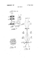
- FIG. 1 shows diagrammatically the layout of an electron probe instrument
- FIG. 2 is a ray diagram showing the orthodox scanning system for covering an area of a specimen surface
- FIG. 3 is a similar ray diagram showing the previously proposed system for obtaining electron channelling (pseudo-Kikuchi) effects by the use of the existing double-deflection coil system;
- FIG. 4 is a ray diagram showing the system according to the invention, employing a single set of scanning coils in conjunction with a lens used for deflection;
- FIG. 5 is a diagram to illustrate the advantage of scanning by a spiral scan instead of a straightforward raster.
- the secondary electrons or the back-scattered primary electrons emerging from the point of impact on the specimen surface are collected at D to produce a signal that is amplified and used to control the brightness of the spot of a cathode ray tube T, the beam of which is deflected in synchronism with the primary electron beam, by a common scanning generator B.
- a two-dimensional image is built up on the screen of the tube T, showing the spatial distribution over the scanned area of the specimen surface, of some phenomenon which produces a variation in the backscatter, such as topography or electrical or magnetic state.
- the two sets of deflection coils are contained in the back bore of the final lens, which is almost invariably electromagnetic.
- the final lens has a small exit aperture AI, as illustrated in FIG. 2, which is a ray diagram showing the lower part of the column of the instrument of FIG. 1.
- the aim is to vary in a cyclic manner the angle of impact of the beam on the specimen surface.
- the effect in question is observable even when scanning an appreciable area of a specimen, provided the scanned area is a single crystal, it is much preferred to examine the effect at a single spot. This has been done by leaving the beam undeflected and by rocking the specimen about two orthogonal axes perpendicular to the electron-optical axis A and passing through the point of impact.
- the information was again reproduced in the form of a two-dimensional image on the screen of the cathode ray tube T, with angular deflection of the primary beam in two directions represented in the image by linear displacement of the spot of the screen in two linear directions.
- the resulting image displays a series of intersecting light and dark bands from which information can be obtained on the crystal structure at the point of impact.
- the final lens L3 has its current adjusted so that it focusses the image from the plane of the coils D1 to form a reduced image at the specimen surface.
- the plane of the deflecting coils D1 and the point of impact on the specimen surface are conjugate points with respect to the lens L3.
- the lens L3 also acts as part of focussing deflection system. For, by its normal lens action, it refracts back towards the electronoptical axis A any ray that passes through it off the axis.
- this lens is deflecting the beam back towards the axis to a degree dependent on its extent away from the axis, so as well as being brought to a focus at the specimen surface the beam is also caused always to impinge on a fixed spot on the specimen surface.
- the deflection coils D1 cause the beam to scan back and forth, the beam rocks angularly about a fixed point of impact on the specimen surface. In a typical case the total angular scan in each case is 8 degrees, and the area of the region of impact is about microns (i.e.
- the actual diameter of the beam at this point is only about one micron, but the scanning action, as well as the focussing action, of the lens L3 is subject to the spherical aberration of the lens, which means that the beam crosses the electronoptical axis at a point nearer the lens when the deflection is large than when it is small, so that the point of impact does in fact move during scanning.
- the position of the specimen surface is therefore chosen at a point on the axis A where there is a circle of least confusion rather than the theoretical focus, and this circle is, as indicated, about 10 microns in diameter.
- the coils D1 can cause the beam to scan the fixed point on the specimen surface in a solid angle by means of what we can call an angular raster, that is to say, by applying a rapid sawtooth time base voltage, analogous to the line scan in a television-type raster, to the deflection coils in one plane and a slower saw-tooth voltage, analogous to a television frame scan, to the coils in the other plane.
- the image on the screen of the cathode ray tube T is in the form of a two-dimensional raster obtained exactly like a television raster from the same two saw-tooth voltages.
- the minimum area scanned at the region of impact on the specimen surface can be reduced by correcting for the spherical aberration of the lens L3.
- the method of moving the image I is by varying the current in the lens L2, or in lenses L1 and L2.
- By appropriately manipulating the current in these three coils we are able to make the apparent origin of the primary scan, as viewed from the final lens L3, move along the axis as required, and this origin is always arranged to coincide with the position of the image I.
- the second basic way of correcting for spherical aberration is by varying directly the current in the final lens L3 in step with the scanning, so as to vary its effective focal length in step with the radial distance from the axis A at which the electron beam passes through the lens.
- the image I remains fixed and so the primary scan can be by the single set of coils D1, and the coils D2 and E can be omitted.
- an iron-cored electromagnetic lens of the dimensions and power used for the lens L3 has a very substantial inductance and so it would be virtually impossible to vary the current in step with the line scan of a typical scanning raster, in which the total time taken for a frame may be of the order of a few seconds, and the time for a single line (or rather a single angular scan by the coils D1 in the line direction) may be only a hundredth of a second.
- FIG. 5 an image in two-dimensional form (as it would be displayed on the screen of the cathode ray tube) comprising a series of straight lines making up a frame, as in a television-type raster.
- the raster is square, although this is by no means essential.
- this correcting signal As the correcting signal to be applied to the winding of the lens L3 depends only on this angular deflection, this correcting signal correspondingly only has to vary at frame frequency. Thus the correction can be applied with acceptable frame periods of the order of a few seconds, or less. It can be shown that, for a given maximum rate of change of the correcting signal, a given solid angle can be covered with a polar scan in half the time taken for only one line of a cartesian or raster-type scan.
- the particular arrangement of the condenser lens system and apertures may be varied as desired, as well as the position of the primary scanning coils.
- the aperture A2 may be above the lens L2, and there may be fewer or more than two lenses in the condenser lens system.
- the only important thing is that an image is formed on the axis A at a point which, with respect to the final lens, is conjugate to the specimen surface, and a primary scanning system deflects the beam angularly away from the axis with this point as origin, the final lens itself forming the secondary scanning system that deflects the beam back onto the axis at the specimen surface.
- an air-cored lens or so-called mini-lens is preferably used for the final lens as its self-inductance is very much lower than that of an orthodox iron-cored lens.
- the main lens could be an orthodox iron-cored lens carrying a constant current and the correcting signal could be applied to an air-cored auxiliary lens.
- the deflection rates may be arranged to obtain a constant velocity of the spot over the screen of the cathode ray tube, i.e. so that the angular velocity of scanning varies inversely with radial deflection.
- the radial deflection passes straight through the zero point from one limit to the other and back again, as this avoids the need for a flyback, which is necessarily rapid.
- the invention may be applied to an instrument specially built for the purpose, not by modifying an existing instrument.
- the image should be formed from back-scattered electrons.
- it could be formed from the specimen current or, where the specimen is of photo-luminescent material, the signal detected could be a light signal.
- Electron probe apparatus comprising a source of electrons, beam forming means, said beam-forming means forming a beam from said electrons along an axis and forming an image of said source at a first point spaced along said axis from said source, first beamdeflection means, said deflection means being effective on said axis at said first point, means feeding a sawtooth deflection signal to said beam-deflecting means whereby to cause said beam to be deflected back and forth laterally from said axis in an angular manner centered on said first point, means defining an aperture around said axis at a second point on said axis further from said source than said first point, electron lens means disposed around said a erture,and serving to focus said beam to a spot at a t 1rd point on said axis,
- said electron lens serving simultaneously to deflect said beam back towards said axis in dependence on the departure of said beam from said axis whereby said electron lens simultaneously forms second beam-deflection means causing said spot to remain substantially on said axis as said beam is scanned back and forth by said first beam-deflection means so that said beam effectively rocks angularly about said third point in step with said saw-tooth deflection signal, means for locating a specimen surface at said third point, detector means adapted to detect the response at said specimen surface to the impact of said beam, and display means connected to said detector means and said saw-tooth deflection signal feeding means to produce a visual display of the response of said detector means in accordance with the angular variation of the impact of the beam on said specimen surface.
- Electron probe apparatus as set forth in claim 1 including means supplying a correcting signal to said electron lens, said correcting signal being variable in synchronism with said first beam-deflecting means and serving to correct the path of said beam for spherical aberration of said lens.
- Electron probe apparatus as set forth in claim 2 wherein said first beam-deflecting means are such as to cause said beam to sweep out a conical path of slowly varying cone angle.
- Electron probe apparatus as set forth in claim 3 wherein said display means are such as to produce a two-dimensional display by a spiral scan.
Abstract
In electron probe apparatus modified or designed to display electron-channelling (pseudo-Kikuchi) effects by subjecting a point on a specimen surface to an electron beam scanned through a varying angle, the final lens of the beam forming system is employed as a deflection element in that an image of the source is formed in the plane of deflection means and that this plane and the specimen surface are made conjugate points with respect to the final lens. To facilitate corrections for spherical aberration in the scanning, the scanning is preferably performed on polar co-ordinates, with the beam sweeping out a conical path of slowly varying cone angle, and the result is displayed as a spirally scanned image.
Description
United States Patent Van-Essen et al.
Nov. 7, 1972 ELECTRON BEAM APPARATUS Cambridge Scientific Instruments Limited Filed: Jan. 21, 1971 Appl. No.: 108,408
Assignee:
[30] Foreign Application Priority Data Jan. 21, 1970 Great Britain ..2,829/70 July 2, 1970 Great Britain ..32,059/70 References Cited UNITED STATES PATENTS 12/1970 Morris et al. ..250/49.5
3,453,485 7/1969 Herrmann et al.....250/49.5 x 2,886,727 5/1959 Haine ..250/49.5 x 3,585,382 6/1971 Suganuma ..250/49.5
Primary Examiner-William F. Lindquist Attorney-Scrivener, Parker, Scrivener & Clarke [57] ABSTRACT I In electron probe apparatus modified or designed to display electron-channelling (pseudo-Kikuchi) effects by subjecting a point on a specimen surface to an electron beam scanned through a varying angle, the final lens of the beam forming system is employed as a deflection element in that an image of the source is formed in the plane of deflection means and that this plane and the specimen surface are made conjugate points with respect to the final lens. To facilitate corrections for spherical aberration in the scanning, the scanning is preferably performed on polar co-ordinates, with the beam sweeping out a conical path of slowly varying cone angle, and the result is displayed as a spirally scanned image.
4 Claims, 5 Drawing Figures am awn E I -E W t//l ELECTRON BEAM APPARATUS This invention relates to electron beam apparatus, primarily to the use of a modified form of scanning electron microscope, that is to say, an instrument in which a fine electron beam or probe is formed by lenses and caused to impinge on the surface of a specimen, the resulting secondary electrons, or back-scattered primary electrons, or the current from the specimen itself, being used to form an image on a recording device, such as the screen of a cathode ray tube, scanned in synchronism with the probe or specimen. However, the invention may also be applied to an instrument in which it is electromagnetic radiation (such as X-rays or light) generated by the impingement of the bean rather than the electrons that are detected and analysed.
In the normal electron beam apparatus of this kind, originally developed by Oatley, McMullan, Cosslett, Duncumb and others, a beam of electrons from an electron gun is forrned by a condenser lens system, usually comprising first and second electromagnetic lenses, and the resulting image of the source formed on the electron-optical axis, is de-magnified by a final, or objective, lens, again electromagnetic, of short focal length to form a reduced image on the surface of the specimen. Scanning coils mounted within the back bore of the objective lens deflect the beam in two mutually perpendicular directions, both transverse to the axis of the beam. Duncumb arranged two sets of scanning coils, axially spaced apart, for each scanning direction to deflect the beam away from the axis and then back towards it, so that the beam always passes through the relatively small final aperture.
Using an instrument of this kind Coates has shown (Scanning Electron Microscopy, 1969, Proceedings of the Second Annual Scanning Electron Microscope Symposium, April 1969) an electron channelling effect in single crystal specimens akin to the Kikuchi effect observed by crystallographic electron diffraction, and he has termed this a pseudo-Kikuchi effect. The contrast that produces the pattern in the image is the result of variation in the angle of the incident beam with respect to the crystal structure as the beam scans back and forth; thus in such an arrangement an angular scan is an essential part of the method and so necessarily the pattern produced is that from a substantial area of the specimen, for example two or three millimeters square. The resolution is limited by the angular divergence of the beam, which is in an under-focussed condition.
An alternative arrangement has been proposed in which the scanning is switched off, the beam remaining on a fixed axis, while the specimen is rocked about two orthogonal axes passing through the point of impingement. Mechanical considerations set a lower limit on the area from which patterns can be generated, and make specimen manipulation difficult.
Another proposal has been to alter the relative currents in the upper and lower sets of scanning coils until the cross-over point, instead of being just above the final aperture in the region of the front pole piece of the final lens, is actually at the specimen surface. Then operation of the scanning coils causes the beam to rock about its point of impingement on the specimen. In practice this point is not a geometrical focus but a disc of confusion whose area is determined by the electron optical aberrations of the scanning coils; these aberrations typically give rise to a disc of confusion of the order of microns diameter. The final lens is either turned off or operated in an under-focussed condition.
The aim of the present invention is to provide an improved method of obtaining pseudo-Kikuchi patterns from small areas using electron beam apparatus of the general kind indicated in the opening paragrahhs above.
According to the invention there is now proposed electron probe apparatus comprising means for forming a fine probe or beam of electrons that forms an image of a source substantially within a scanning coil system that is capable of deflecting the beam back and forth, and the resulting laterally scanned image is formed in the object plane of a lens that serves, not only for its usual purpose of focussing the image, but also for deflecting the beam back onto the optical axis at the surface of the specimen itself. Thus this lens forms part of the scanning system that causes the beam to rock angularly about its point of impact on the specimen.
In an existing scanning electron probe instrument this result can be obtained simply by employing as the scanning lens the final or objective lens of the normal focussing system. Where there are two sets of scanning coils in the existing instrument, the first deflection of the scanning system is obtained by the first set of coils alone and the second set of coils is removed, or at least switched off.
It will be understood that, as in known instruments, the scanning will normally be done in two orthogonal directions perpendicular to the electron-optical axis.
The aim is to derive information on the crystal structure at virtually a single point, i.e. at as small an area of the specimen as possible. The unavoidable spherical aberration of the lens will result in variations of the point of impact with deflection, making the area covered larger than desirable. This can be offset by applying a correction signal, that varies in synchronism with the scanning signal.
The correction can be applied by rhythmically shifting, in synchronism with the scanning deflection, the apparent position along the electron-optical axis, of the image of the source that forms the object of the final lens. For this purpose we retain the two axially spaced sets of scanning coils and may even add a third set, and we vary the current in them appropriately.
Alternatively, we can correct for spherical aberration of the final lens by varying directly the current in that lens in step with the scanning deflection. However, the high inductance of an iron-cored electromagnetic lens severely limits the rate of change of such a correcting signal and consequently makes the overall scanning speed very slow; this seriously restricts the usefulness of the instrument. Therefore, we prefer to use for the final lens an air-cored so-called mini-lens or solenoid type lens. Or we may retain an iron-cored main final lens but apply the correction current to an auxiliary lens, preferably air-cored. Instead, or in addition, we propose, according to a further feature of the invention, that instead of using a normal orthogonal raster in a series of lines to build up a frame, we should use a polar coordinate system of scanning, with a relatively rapid circular deflection and slow radial deflection. In
this way a given area (in the reproduced image) representing a given solid angular range in the impact of the beam, can be covered in a relatively short time yet with the radius vector changing only relatively slowly, allowing the correcting signal (which needs to vary only with the radius vector) to be applied.
The invention will now be further described with reference to the accompanying drawings, in which:
FIG. 1 shows diagrammatically the layout of an electron probe instrument;
FIG. 2 is a ray diagram showing the orthodox scanning system for covering an area of a specimen surface;
FIG. 3 is a similar ray diagram showing the previously proposed system for obtaining electron channelling (pseudo-Kikuchi) effects by the use of the existing double-deflection coil system;
FIG. 4 is a ray diagram showing the system according to the invention, employing a single set of scanning coils in conjunction with a lens used for deflection; and
FIG. 5 is a diagram to illustrate the advantage of scanning by a spiral scan instead of a straightforward raster.
Referring first to FIG. 1, an orthodox scanning electron microscope, for examining a selected area of a specimen surface comprises a source in the form of an electron gun G, the electrons from which are formed into a beam by first and second condenser lenses L1 and L2 that produce a reduced image of the source, and this image is further reduced by the final or probeforming lens L3, so that the diameter of the point of impact on the surface of a specimen S in the path of the beam and on its electron-optical axis A may be of the order of 50 Angstrom units or less. Pairs of deflection coils DI and D2 cause the beam not to impinge on a single point but to scan an area of the specimen in a raster similar to a television scanning raster. For reasons which will be described with reference to FIG. 2, there is not a single set of deflection coils for each of the two mutually perpendicular scanning directions (line and frame) but two sets spaced apart long the axis A, so that the beam is first deflected away from the axis and then back towards it.
The secondary electrons or the back-scattered primary electrons emerging from the point of impact on the specimen surface are collected at D to produce a signal that is amplified and used to control the brightness of the spot of a cathode ray tube T, the beam of which is deflected in synchronism with the primary electron beam, by a common scanning generator B. In this way a two-dimensional image is built up on the screen of the tube T, showing the spatial distribution over the scanned area of the specimen surface, of some phenomenon which produces a variation in the backscatter, such as topography or electrical or magnetic state.
In practice, in a typical instrument, the two sets of deflection coils are contained in the back bore of the final lens, which is almost invariably electromagnetic. To keep the spot size down one must restrict spherical aberration and so the final lens has a small exit aperture AI, as illustrated in FIG. 2, which is a ray diagram showing the lower part of the column of the instrument of FIG. 1. This explains the purpose of the two axially spaced sets of deflection coils D1 and D2, namely to ensure that, despite being deflected laterally, the beam always passes through this aperture which is placed close to the principal plane of the lens.
In the mode of operation necessary to exhibit the electron-channelling effect, also referred to as the pseudo-Kikuchi effect, in a scanning electron microscope, the aim is to vary in a cyclic manner the angle of impact of the beam on the specimen surface. Although the effect in question is observable even when scanning an appreciable area of a specimen, provided the scanned area is a single crystal, it is much preferred to examine the effect at a single spot. This has been done by leaving the beam undeflected and by rocking the specimen about two orthogonal axes perpendicular to the electron-optical axis A and passing through the point of impact. The result was reproduced as a two-dimensional image on the screen of a cathode ray tube with the X and Y deflections synchronized with the two angular deflections of the specimen. Another method already proposed is that illustrated in FIG. 3, in which the aperture A1 of the final lens was enlarged and the focus of the lens system formed by the first two lenses L1 and L2 was shifted downwards until it coincided with the specimen surface. At the same time, the relative strengths of the coils D1 and D2 were adjusted so that they, in deflecting the beam, brought it back to the axis A at the specimen surface instead of at the aperture Al. The beam then rocked about the point of impact. The information was again reproduced in the form of a two-dimensional image on the screen of the cathode ray tube T, with angular deflection of the primary beam in two directions represented in the image by linear displacement of the spot of the screen in two linear directions. The resulting image displays a series of intersecting light and dark bands from which information can be obtained on the crystal structure at the point of impact.
Now in the arrangement according to the present invention, shown in FIG. 4, we do not use the second set of deflection coils D2 at all, at least not for scanning. We insert an apertureA2 following the second lens L2, much smaller than the aperture previously present at this point, to reduce the divergence of the beam (for example an aperture of only 10*mm diameter) and we adjust the current in the lenses L1 and L2 so that an image of the source is produced at a point I on the axis A in the plane of the remaining set of deflection coils D1. A saw-tooth voltage is applied to these coils to deflect the beam. (It is deflected in each of two perpendicular planes, but we will only consider one plane here for convenience). The final lens L3 has its current adjusted so that it focusses the image from the plane of the coils D1 to form a reduced image at the specimen surface. Thus the plane of the deflecting coils D1 and the point of impact on the specimen surface are conjugate points with respect to the lens L3. However, in addition to acting as a focusing lens, the lens L3 also acts as part of focussing deflection system. For, by its normal lens action, it refracts back towards the electronoptical axis A any ray that passes through it off the axis. Thus, as the deflection coils D1 are causing the beam to scan back and forth across the aperture A1 of the final lens L3, (this aperture being now large, for example of the order of 2 mm) this lens is deflecting the beam back towards the axis to a degree dependent on its extent away from the axis, so as well as being brought to a focus at the specimen surface the beam is also caused always to impinge on a fixed spot on the specimen surface. Thus, as the deflection coils D1 cause the beam to scan back and forth, the beam rocks angularly about a fixed point of impact on the specimen surface. In a typical case the total angular scan in each case is 8 degrees, and the area of the region of impact is about microns (i.e. l0' mm) in diameter. The actual diameter of the beam at this point is only about one micron, but the scanning action, as well as the focussing action, of the lens L3 is subject to the spherical aberration of the lens, which means that the beam crosses the electronoptical axis at a point nearer the lens when the deflection is large than when it is small, so that the point of impact does in fact move during scanning. The position of the specimen surface is therefore chosen at a point on the axis A where there is a circle of least confusion rather than the theoretical focus, and this circle is, as indicated, about 10 microns in diameter.
As in the previously proposed arrangement described with reference to FIG. 3, the coils D1 can cause the beam to scan the fixed point on the specimen surface in a solid angle by means of what we can call an angular raster, that is to say, by applying a rapid sawtooth time base voltage, analogous to the line scan in a television-type raster, to the deflection coils in one plane and a slower saw-tooth voltage, analogous to a television frame scan, to the coils in the other plane. The image on the screen of the cathode ray tube T is in the form of a two-dimensional raster obtained exactly like a television raster from the same two saw-tooth voltages.
The minimum area scanned at the region of impact on the specimen surface can be reduced by correcting for the spherical aberration of the lens L3.
There are two basic ways of doing this. It is well known that the effect of spherical aberration is to cause those electrons which pass through the lens in zones spaced radially a substantial distance away from the axis to be brought to a focus at a point on the axis nearer to the lens than those electrons which pass through the lens close to the axis. We can therefore compensate for this by moving the image I, formed by the condenser lens system L1 and L2, rythmically back and forth along the axis during scanning, so that it is moved nearer to the lens L3 at large scanning angles than when the scanning angle is smaller. Then the image is brought to a focus at a constant point on the axis, i.e. exactly at the specimen surface, throughout the scanning cycle.
The method of moving the image I is by varying the current in the lens L2, or in lenses L1 and L2. At the same time we must modify the primary scanning system to allow for the axial shift of the image I and so instead of using the single pair of coils D1, we use in practice also the coils D2 and we may even use a third pair of coils, indicated at B. By appropriately manipulating the current in these three coils we are able to make the apparent origin of the primary scan, as viewed from the final lens L3, move along the axis as required, and this origin is always arranged to coincide with the position of the image I. In practice we vary the current in the second condenser lens L2 to move the image I along the axis A in step with the scanning (the point I moving downwards in FIG. 3 in step with the scanning amplitude), and we derive a signal from the current in the coil L2 and use this signal to control the ratios of the currents in the coils D1 and D2 (and coils E, if present) so that the apparent origin of the lateral scan caused by these coils coincides with the image I.
The second basic way of correcting for spherical aberration is by varying directly the current in the final lens L3 in step with the scanning, so as to vary its effective focal length in step with the radial distance from the axis A at which the electron beam passes through the lens. In this case the image I remains fixed and so the primary scan can be by the single set of coils D1, and the coils D2 and E can be omitted.
However, an iron-cored electromagnetic lens of the dimensions and power used for the lens L3 has a very substantial inductance and so it would be virtually impossible to vary the current in step with the line scan of a typical scanning raster, in which the total time taken for a frame may be of the order of a few seconds, and the time for a single line (or rather a single angular scan by the coils D1 in the line direction) may be only a hundredth of a second.
To allow the desired correction to be applied is to use, in place of the two angular scans in mutually perpendicular directions, a scan employing polar co-ordinates with the angular signal changing rapidly and the radial signal changing slowly. Thus the beam sweeps out a conical path of slowly varying apex angle. In FIG. 5 is shown an image in two-dimensional form (as it would be displayed on the screen of the cathode ray tube) comprising a series of straight lines making up a frame, as in a television-type raster. In the example shown the raster is square, although this is by no means essential. When it is remembered that linear distances from the center of the square image correspond to angular departures of the primary beam from the electron-optical axis A, it will be seen that the angular departure varies widely during every line and during the middle line it varies within one line right through zero from a value of 1% 2 times the maximum value in one direction to 1% 2 times the maximum value in the other direction. It would only be possible to vary the current in the lens L3 in step with this for correcting purposes if the line frequency and therefore the whole scanning cycle were to be so slow as to be virtually unacceptable.
If, however, we scan in a circular path, with the primary beam forming the genatrix of a cone having its apex at the specimen surface, with beam describing a path rapidly round the surface of the cone while the cone angle changes slowly from zero to a maximum, while the spot on the screen of the cathode tube follows a corresponding spiral path, as indicated by the superimposed spiral image in FIG. 5, we can cover the same image area (i.e. the same solid angle) with the same definition, but with the angular deflection of the beam with respect to the axis A changing only at frame frequency instead of line frequency. As the correcting signal to be applied to the winding of the lens L3 depends only on this angular deflection, this correcting signal correspondingly only has to vary at frame frequency. Thus the correction can be applied with acceptable frame periods of the order of a few seconds, or less. It can be shown that, for a given maximum rate of change of the correcting signal, a given solid angle can be covered with a polar scan in half the time taken for only one line of a cartesian or raster-type scan.
it will be understood that, to apply the polar scan, it-
is not necessary to employ special coils at D1. The existing mutually perpendicular pairs of coils could be used and fed with the appropriate sine and cosine deflection signals to produce the spiral scan.
It will be understood that the particular arrangement of the condenser lens system and apertures may be varied as desired, as well as the position of the primary scanning coils. For example, the aperture A2 may be above the lens L2, and there may be fewer or more than two lenses in the condenser lens system. The only important thing is that an image is formed on the axis A at a point which, with respect to the final lens, is conjugate to the specimen surface, and a primary scanning system deflects the beam angularly away from the axis with this point as origin, the final lens itself forming the secondary scanning system that deflects the beam back onto the axis at the specimen surface.
According to a further feature of the invention, an air-cored lens or so-called mini-lens is preferably used for the final lens as its self-inductance is very much lower than that of an orthodox iron-cored lens. Alternatively, the main lens could be an orthodox iron-cored lens carrying a constant current and the correcting signal could be applied to an air-cored auxiliary lens.
Where the spiral scan is used, the deflection rates may be arranged to obtain a constant velocity of the spot over the screen of the cathode ray tube, i.e. so that the angular velocity of scanning varies inversely with radial deflection. This gives constant brightness over the whole image and moreover it can be shown that, for a given maximum rate of change of the correction signal, a given solid angle can be covered in only a quarter of the time taken for a single line of a cartesian scan. Preferably also the radial deflection passes straight through the zero point from one limit to the other and back again, as this avoids the need for a flyback, which is necessarily rapid.
It will also be understood that the invention may be applied to an instrument specially built for the purpose, not by modifying an existing instrument. There could be a different condenser lens system from that shown, employing perhaps only one lens instead of two. Also, it is not essential that the image should be formed from back-scattered electrons. For example, it could be formed from the specimen current or, where the specimen is of photo-luminescent material, the signal detected could be a light signal.
What we claim is:
1. Electron probe apparatus comprising a source of electrons, beam forming means, said beam-forming means forming a beam from said electrons along an axis and forming an image of said source at a first point spaced along said axis from said source, first beamdeflection means, said deflection means being effective on said axis at said first point, means feeding a sawtooth deflection signal to said beam-deflecting means whereby to cause said beam to be deflected back and forth laterally from said axis in an angular manner centered on said first point, means defining an aperture around said axis at a second point on said axis further from said source than said first point, electron lens means disposed around said a erture,and serving to focus said beam to a spot at a t 1rd point on said axis,
said third point being farther from said source than said first and second points, said electron lens serving simultaneously to deflect said beam back towards said axis in dependence on the departure of said beam from said axis whereby said electron lens simultaneously forms second beam-deflection means causing said spot to remain substantially on said axis as said beam is scanned back and forth by said first beam-deflection means so that said beam effectively rocks angularly about said third point in step with said saw-tooth deflection signal, means for locating a specimen surface at said third point, detector means adapted to detect the response at said specimen surface to the impact of said beam, and display means connected to said detector means and said saw-tooth deflection signal feeding means to produce a visual display of the response of said detector means in accordance with the angular variation of the impact of the beam on said specimen surface.
2. Electron probe apparatus as set forth in claim 1 including means supplying a correcting signal to said electron lens, said correcting signal being variable in synchronism with said first beam-deflecting means and serving to correct the path of said beam for spherical aberration of said lens.
3. Electron probe apparatus as set forth in claim 2 wherein said first beam-deflecting means are such as to cause said beam to sweep out a conical path of slowly varying cone angle.
4. Electron probe apparatus as set forth in claim 3 wherein said display means are such as to produce a two-dimensional display by a spiral scan.
Claims (4)
1. Electron probe apparatus comprising a source of electrons, beam forming means, said beam-forming means forming a beam from said electrons along an axis and forming an image of said source at a first point spaced along said axis from said source, first beam-deflection means, said deflection means being effective on said axis at said first point, means feeding a saw-tooth deflection signal to said beam-deflecting means whereby to cause said beam to be deflected back and forth laterally from said axis in an angular manner centered on said first point, means defining an aperture around said axis at a second point on said axis further from said source than said first point, electron lens means disposed around said aperture and serving to focus said beam to a spot at a third point on said axis, said third point being farther from said source than said first and second points, said electron lens serving simultaneously to deflect said beam back towards said axis in dependence on the departure of said beam from said axis whereby said electron lens simultaneously forms second beam-deflection means causing said spot to remain substantially on said axis as said beam is scanned back and forth by said first beam-deflection means so that said beam effectively rocks angularly about said third point in step with said sawtooth deflection signal, means for locating a specimen surface at said third point, detector means adapted to detect the response at said specimen surface to the impact of said beam, and display means connected to said detector means and said saw-tooth deflection signal feeding means to produce a visual display of the response of said detector means in accordance with the angular variation of the impact of the beam on said specimen surface.
2. Electron probe apparatus as set forth in claim 1 including means supplying a correcting signal to said electron lens, said correcting signal being variable in synchronism with said first beam-deflecting means and serving to correct the path of said beam for spherical aberration of said lens.
3. Electron probe apparatus as set forth in claim 2 wherein said first beam-deflecting means are such as to cause said beam to sweep out a conical path of slowly varying cone angle.
4. Electron probe apparatus as set forth in claim 3 wherein said display means are such as to produce a two-dimensional display by a spiral scan.
Applications Claiming Priority (2)
| Application Number | Priority Date | Filing Date | Title |
|---|---|---|---|
| GB282970 | 1970-01-21 | ||
| GB3205970 | 1970-07-02 |
Publications (1)
| Publication Number | Publication Date |
|---|---|
| US3702398A true US3702398A (en) | 1972-11-07 |
Family
ID=26237761
Family Applications (1)
| Application Number | Title | Priority Date | Filing Date |
|---|---|---|---|
| US108408A Expired - Lifetime US3702398A (en) | 1970-01-21 | 1971-01-21 | Electron beam apparatus |
Country Status (5)
| Country | Link |
|---|---|
| US (1) | US3702398A (en) |
| JP (1) | JPS5425391B1 (en) |
| DE (1) | DE2102616A1 (en) |
| FR (1) | FR2075739A5 (en) |
| GB (1) | GB1284061A (en) |
Cited By (14)
| Publication number | Priority date | Publication date | Assignee | Title |
|---|---|---|---|---|
| US3801792A (en) * | 1973-05-23 | 1974-04-02 | Bell Telephone Labor Inc | Electron beam apparatus |
| US3801784A (en) * | 1972-04-14 | 1974-04-02 | Research Corp | Scanning electron microscope operating in area scan and angle scan modes |
| EP0013738A1 (en) * | 1979-01-18 | 1980-08-06 | International Business Machines Corporation | Method and apparatus for producing a high brightness electron beam |
| FR2605739A1 (en) * | 1986-10-27 | 1988-04-29 | Atomika Tech Physik Gmbh | METHOD OF SPIRAL SCANNING BY A PARTICLE BEAM |
| US4780216A (en) * | 1986-11-19 | 1988-10-25 | Olin Corporation | Calcium hypochlorite sanitizing compositions |
| DE3924605A1 (en) * | 1988-07-25 | 1990-02-01 | Hitachi Ltd | GRID ELECTRON MICROSCOPE |
| US4990779A (en) * | 1989-06-06 | 1991-02-05 | Nippon Steel Corporation | Method and apparatus for evaluating strains in crystals |
| US20020125444A1 (en) * | 2001-01-17 | 2002-09-12 | Nikon Corporation | Illumination-beam scanning configurations and methods for charged-particle-beam microlithography |
| US20040051542A1 (en) * | 2002-07-04 | 2004-03-18 | University Of Bristol Of Senate House | Scanning probe microscope |
| US20040232321A1 (en) * | 2001-02-06 | 2004-11-25 | University Of Bristol Of Senate House | Scanning near-field optical microscope |
| US6930308B1 (en) * | 2002-07-11 | 2005-08-16 | Kla-Tencor Technologies Corporation | SEM profile and surface reconstruction using multiple data sets |
| US20100327179A1 (en) * | 2009-06-26 | 2010-12-30 | Carl Zeiss Nts Gmbh | Charged particle beam column and method of operating same |
| US20110108736A1 (en) * | 2009-11-09 | 2011-05-12 | Carl Zeiss Nts Gmbh | SACP Method and Particle Optical System for Performing the Method |
| WO2018122015A1 (en) * | 2016-12-30 | 2018-07-05 | Imec Vzw | Characterization of regions with different crystallinity in materials |
Families Citing this family (2)
| Publication number | Priority date | Publication date | Assignee | Title |
|---|---|---|---|---|
| NL7204859A (en) * | 1972-04-12 | 1973-10-16 | ||
| JPS5788659A (en) * | 1980-11-21 | 1982-06-02 | Jeol Ltd | Electron ray device |
Citations (4)
| Publication number | Priority date | Publication date | Assignee | Title |
|---|---|---|---|---|
| US2886727A (en) * | 1955-12-12 | 1959-05-12 | Vickers Electrical Co Ltd | Electron optical apparatus |
| US3453485A (en) * | 1966-03-15 | 1969-07-01 | Siemens Ag | Deflector system for corpuscular-beam apparatus |
| US3549883A (en) * | 1968-10-07 | 1970-12-22 | Gen Electric | Scanning electron microscope wherein an image is formed as a function of specimen current |
| US3585382A (en) * | 1968-05-28 | 1971-06-15 | Jeol Ltd | Stereo-scanning electron microscope |
-
1970
- 1970-01-21 GB GB3205/70A patent/GB1284061A/en not_active Expired
-
1971
- 1971-01-20 DE DE19712102616 patent/DE2102616A1/en active Pending
- 1971-01-20 FR FR7101733A patent/FR2075739A5/fr not_active Expired
- 1971-01-21 JP JP152871A patent/JPS5425391B1/ja active Pending
- 1971-01-21 US US108408A patent/US3702398A/en not_active Expired - Lifetime
Patent Citations (4)
| Publication number | Priority date | Publication date | Assignee | Title |
|---|---|---|---|---|
| US2886727A (en) * | 1955-12-12 | 1959-05-12 | Vickers Electrical Co Ltd | Electron optical apparatus |
| US3453485A (en) * | 1966-03-15 | 1969-07-01 | Siemens Ag | Deflector system for corpuscular-beam apparatus |
| US3585382A (en) * | 1968-05-28 | 1971-06-15 | Jeol Ltd | Stereo-scanning electron microscope |
| US3549883A (en) * | 1968-10-07 | 1970-12-22 | Gen Electric | Scanning electron microscope wherein an image is formed as a function of specimen current |
Cited By (19)
| Publication number | Priority date | Publication date | Assignee | Title |
|---|---|---|---|---|
| US3801784A (en) * | 1972-04-14 | 1974-04-02 | Research Corp | Scanning electron microscope operating in area scan and angle scan modes |
| US3801792A (en) * | 1973-05-23 | 1974-04-02 | Bell Telephone Labor Inc | Electron beam apparatus |
| EP0013738A1 (en) * | 1979-01-18 | 1980-08-06 | International Business Machines Corporation | Method and apparatus for producing a high brightness electron beam |
| FR2605739A1 (en) * | 1986-10-27 | 1988-04-29 | Atomika Tech Physik Gmbh | METHOD OF SPIRAL SCANNING BY A PARTICLE BEAM |
| US4780216A (en) * | 1986-11-19 | 1988-10-25 | Olin Corporation | Calcium hypochlorite sanitizing compositions |
| DE3924605A1 (en) * | 1988-07-25 | 1990-02-01 | Hitachi Ltd | GRID ELECTRON MICROSCOPE |
| US4990779A (en) * | 1989-06-06 | 1991-02-05 | Nippon Steel Corporation | Method and apparatus for evaluating strains in crystals |
| US20020125444A1 (en) * | 2001-01-17 | 2002-09-12 | Nikon Corporation | Illumination-beam scanning configurations and methods for charged-particle-beam microlithography |
| US7498564B2 (en) * | 2001-02-06 | 2009-03-03 | University Of Bristol Of Senate House | Resonant scanning near-field optical microscope |
| US20040232321A1 (en) * | 2001-02-06 | 2004-11-25 | University Of Bristol Of Senate House | Scanning near-field optical microscope |
| US7473887B2 (en) | 2002-07-04 | 2009-01-06 | University Of Bristol Of Senate House | Resonant scanning probe microscope |
| US20040051542A1 (en) * | 2002-07-04 | 2004-03-18 | University Of Bristol Of Senate House | Scanning probe microscope |
| US6930308B1 (en) * | 2002-07-11 | 2005-08-16 | Kla-Tencor Technologies Corporation | SEM profile and surface reconstruction using multiple data sets |
| US20100327179A1 (en) * | 2009-06-26 | 2010-12-30 | Carl Zeiss Nts Gmbh | Charged particle beam column and method of operating same |
| US8129693B2 (en) | 2009-06-26 | 2012-03-06 | Carl Zeiss Nts Gmbh | Charged particle beam column and method of operating same |
| US8558190B2 (en) | 2009-06-26 | 2013-10-15 | Carl Zeiss Microscopy Gmbh | Charged particle beam column and method of operating same |
| US20110108736A1 (en) * | 2009-11-09 | 2011-05-12 | Carl Zeiss Nts Gmbh | SACP Method and Particle Optical System for Performing the Method |
| US9093246B2 (en) | 2009-11-09 | 2015-07-28 | Carl Zeiss Microscopy Gmbh | SACP method and particle optical system for performing the method |
| WO2018122015A1 (en) * | 2016-12-30 | 2018-07-05 | Imec Vzw | Characterization of regions with different crystallinity in materials |
Also Published As
| Publication number | Publication date |
|---|---|
| DE2102616A1 (en) | 1971-07-29 |
| FR2075739A5 (en) | 1971-10-08 |
| JPS5425391B1 (en) | 1979-08-28 |
| GB1284061A (en) | 1972-08-02 |
Similar Documents
| Publication | Publication Date | Title |
|---|---|---|
| US3702398A (en) | Electron beam apparatus | |
| US6259094B1 (en) | Electron beam inspection method and apparatus | |
| US4209702A (en) | Multiple electron lens | |
| US4209698A (en) | Transmission-type charged particle beam apparatus | |
| US3833811A (en) | Scanning electron microscope with improved means for focusing | |
| EP1057203B1 (en) | Particle-optical apparatus involving detection of auger electrons | |
| US6825476B2 (en) | Column for a charged particle beam device | |
| US5747814A (en) | Method for centering a lens in a charged-particle system | |
| US5300775A (en) | Method of selecting a spatial energy spread within an electron beam, and an electron beam apparatus suitable for carrying out such a method | |
| US5345080A (en) | Method of observing electron microscopic images and an apparatus for carrying out of the same | |
| US3786271A (en) | Electron microscopes and micro-analysers | |
| JPH06243814A (en) | Scanning electron microscope | |
| US6653632B2 (en) | Scanning-type instrument utilizing charged-particle beam and method of controlling same | |
| US10636622B2 (en) | Scanning transmission electron microscope | |
| GB2162682A (en) | Method of displaying electron diffraction patterns | |
| US3657593A (en) | Electron microscopy | |
| US3801784A (en) | Scanning electron microscope operating in area scan and angle scan modes | |
| JP3499690B2 (en) | Charged particle microscope | |
| US3849647A (en) | Scanning electron microscope | |
| US3986027A (en) | Stereo scanning microprobe | |
| US5258617A (en) | Method and apparatus for correcting axial coma in electron microscopy | |
| JP2002184336A (en) | Charged particle beam microscope device, charged particle beam application device, charged particle beam microscopic method, charged particle beam inspection method and electron microscope | |
| JP2019164886A (en) | Beam irradiation device | |
| KR100518812B1 (en) | Reduction of aberrations produced by Wien filter in a scanning electron microscope and the like | |
| US4439681A (en) | Charged particle beam scanning device |