SUBSTITUTED OLIGOAZACARBAZOLES FOR LIGHT EMITTING DIODES
[0001] The claimed invention was made by, on behalf of, and/or in connection with one or more of the following parties to a joint university corporation research agreement: Regents of the University of Michigan, Princeton University, The University of Southern California, and the Universal Display Corporation. The agreement was in effect on and before the date the claimed invention was made, and the claimed invention was made as a result of activities undertaken within the scope of the agreement.
FIELD OF THE INVENTION
[0002] The present invention relates to organic light emitting devices (OLEDs). More specifically, the present invention is related to host materials comprising substituted
oligoazacarbazole compounds. These materials may be used in OLEDs to provide devices having improved performance.
BACKGROUND
[0003] Opto-electronic devices that make use of organic materials are becoming increasingly desirable for a number of reasons. Many of the materials used to make such devices are relatively inexpensive, so organic opto-electronic devices have the potential for cost advantages over inorganic devices. In addition, the inherent properties of organic materials, such as their flexibility, may make them well suited for particular applications such as fabrication on a flexible substrate. Examples of organic opto-electronic devices include organic light emitting devices (OLEDs), organic phototransistors, organic photovoltaic cells, and organic
photodetectors. For OLEDs, the organic materials may have performance advantages over conventional materials. For example, the wavelength at which an organic emissive layer emits light may generally be readily tuned with appropriate dopants. [0004] OLEDs make use of thin organic films that emit light when voltage is applied across the device. OLEDs are becoming an increasingly interesting technology for use in applications such as flat panel displays, illumination, and backlighting. Several OLED materials and configurations are described in U.S. Pat. Nos. 5,844,363, 6,303,238, and 5,707,745, which are incorporated herein by reference in their entirety.
[0005] One application for phosphorescent emissive molecules is a full color display. Industry standards for such a display call for pixels adapted to emit particular colors, referred to as "saturated" colors. In particular, these standards call for saturated red, green, and blue pixels. Color may be measured using CIE coordinates, which are well known to the art. [0006] One example of a green emissive molecule is tris(2-phenylpyridine) iridium, denoted Ir(ppy)3, which has the following structure:
[0007] In this, and later figures herein, we depict the dative bond from nitrogen to metal (here, Ir) as a straight line. [0008] As used herein, the term "organic" includes polymeric materials as well as small molecule organic materials that may be used to fabricate organic opto-electronic devices. "Small molecule" refers to any organic material that is not a polymer, and "small molecules" may actually be quite large. Small molecules may include repeat units in some circumstances. For example, using a long chain alkyl group as a substituent does not remove a molecule from the "small molecule" class. Small molecules may also be incorporated into polymers, for example as a pendent group on a polymer backbone or as a part of the backbone. Small molecules may also serve as the core moiety of a dendrimer, which consists of a series of chemical shells built on the core moiety. The core moiety of a dendrimer may be a fluorescent or phosphorescent small molecule emitter. A dendrimer may be a "small molecule," and it is believed that all dendrimers currently used in the field of OLEDs are small molecules.
[0009] As used herein, "top" means furthest away from the substrate, while "bottom" means closest to the substrate. Where a first layer is described as "disposed over" a second layer, the first layer is disposed further away from substrate. There may be other layers between the first and second layer, unless it is specified that the first layer is "in contact with" the second layer. For example, a cathode may be described as "disposed over" an anode, even though there are various organic layers in between.
[0010] As used herein, "solution processible" means capable of being dissolved, dispersed, or transported in and/or deposited from a liquid medium, either in solution or suspension form.
[0011] A ligand may be referred to as "photoactive" when it is believed that the ligand directly contributes to the photoactive properties of an emissive material. A ligand may be referred to as "ancillary" when it is believed that the ligand does not contribute to the photoactive properties of an emissive material, although an ancillary ligand may alter the properties of a photoactive ligand.
[0012] As used herein, and as would be generally understood by one skilled in the art, a first "Highest Occupied Molecular Orbital" (HOMO) or "Lowest Unoccupied Molecular Orbital" (LUMO) energy level is "greater than" or "higher than" a second HOMO or LUMO energy level if the first energy level is closer to the vacuum energy level. Since ionization potentials (IP) are measured as a negative energy relative to a vacuum level, a higher HOMO energy level corresponds to an IP having a smaller absolute value (an IP that is less negative). Similarly, a higher LUMO energy level corresponds to an electron affinity (EA) having a smaller absolute value (an EA that is less negative). On a conventional energy level diagram, with the vacuum level at the top, the LUMO energy level of a material is higher than the HOMO energy level of the same material. A "higher" HOMO or LUMO energy level appears closer to the top of such a diagram than a "lower" HOMO or LUMO energy level.
[0013] As used herein, and as would be generally understood by one skilled in the art, a first work function is "greater than" or "higher than" a second work function if the first work function has a higher absolute value. Because work functions are generally measured as negative numbers relative to vacuum level, this means that a "higher" work function is more negative. On a conventional energy level diagram, with the vacuum level at the top, a "higher" work function is illustrated as further away from the vacuum level in the downward direction. Thus, the definitions of HOMO and LUMO energy levels follow a different convention than work functions.
[0014] More details on OLEDs, and the definitions described above, can be found in US Pat. No. 7,279,704, which is incorporated herein by reference in its entirety.
SUMMARY OF THE INVENTION
[0015] Compounds comprising substituted oligoazacarbazoles of formula I are provided,
, Formula I.
Group Y is selected from the group consisting of:
Each of A, B, C, and D are independently selected from the compound of formula II:
In the compound of formula II, X1 is selected from the group C— R1 and N, X2 is selected from the group C— R2 and N, X3 is selected from the group C— R3 and N, X4 is selected from the group C— R4 and N, X5 is selected from the group C— R5 and N, X6 is selected from the group C— R6 and N, X7 is selected from the group C— R7 and N, and X8 is selected from the group C— R8 and N.
[0016] Groups A, B, C, and D are connected to each other through C— N bonds, and at least one of A, B, C, and D is not carbazole. Group X is an aryl or heteroaryl linker that is optionally further substituted, and Y and X are connected through a C— N bond.
[0017] Ri, R2, R3, R4, R5, R6, R7, and R8 are independently selected from the group consisting of hydrogen, deuterium, halide, alkyl, cycloalkyl, heteroalkyl, arylalkyl, alkoxy, aryloxy, amino, silyl, alkenyl, cycloalkenyl, heteroalkenyl, alkynyl, aryl, heteroaryl, acyl, carbonyl, carboxylic acids, ester, nitrile, isonitrile, sulfanyl, sulfinyl, sulfonyl, phosphino, and combinations thereof. Group Z is selected from the group consisting of dibenzothiphene, dibenzofuran,
dibenzoselenophene, aza-dibenzothiophene, aza-dibenzofuran, and aza-dibenzoselenophene that is optionally further substituted.
[0018] In one aspect,
, where E, F, G and
H are inde endently selected from the group consisting of
[0019] In one aspect, groups E, F, G and H are optionally further substituted with R9, where R9 represents mono, di, tri, or terra substitution, and R9 is independently selected from the group consisting of hydrogen, deuterium, halide, alkyl, cycloalkyl, heteroalkyl, arylalkyl, alkoxy, aryloxy, amino, silyl, alkenyl, cycloalkenyl, heteroalkenyl, alkynyl, aryl, heteroaryl, acyl, carbonyl, carboxylic acids, ester, nitrile, isonitrile, sulfanyl, sulfmyl, sulfonyl, phosphino, and combinations thereof. Each of p, q, r and s can have a value from 0 to 4, and p+q+r+s is at least 1.
[0020] In one aspect, the groups A, B, C, and D are connected to each other through a bond between a carbon at the 3 or 6-position and a nitrogen at the 9-position. In another aspect, Z is 2- dibenzothiophenyl, 4-dibenzothiophenyl, 2-dibenzofuranyl, or 4-dibenzofuranyl. In another aspect, A, B, C, and D are not carbazole.
[0021] In one aspect, Rls R2, R3, R4, R5, R6, R7, and Rg are independently selected from the group consisting of phenyl, biphenyl, triphenyl, terphenyl, naphthalene, phenalene,
phenanthrene, fluorene, chrysene, dibenzothiophene, dibenzofuran, benzofuran, benzothiophene, pyrazole, imidazole, triazole, oxazole, thiazole, oxadiazole, oxatriazole, dioxazole, thiadiazole, pyridine, pyridazine, pyrimidine, pyrazine, triazine, indole, azaindole, benzimidazole, indazole, benzoxazole, benzisoxazole, benzothiazole, quinoline, isoquinoline, cinnoline, quinazoline,
quinoxaline, naphthyridine, phthalazine, pteridine, xanthene, phenothiazine, phenoxazine, benzofuropyridine, furodipyridine, benzothienopyridine and thienodipyridine.
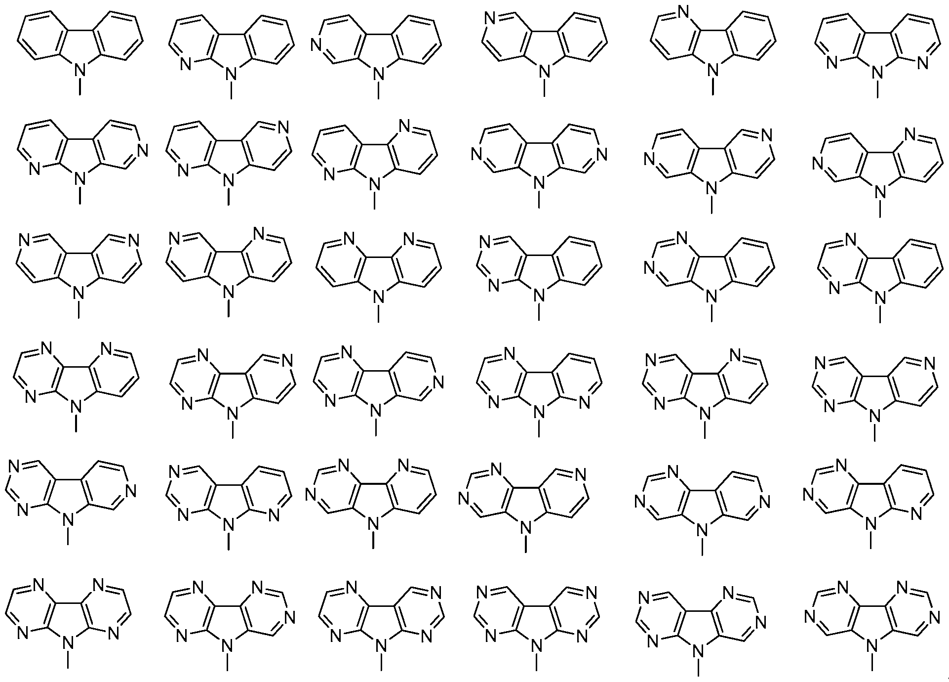
[0022] In one aspect, A, B, C, and D are independently selected from the group consisting of:
[0023] Specific non limiting examples of compounds are provided. In one aspect, the compound is selected from the group consisting of Compound 1 - Compound 35.
[0024] A first device comprising an organic light emitting device is provided. The organic light emitting device further comprises an anode, a cathode, and a first organic layer disposed between the anode and the cathode. The first organic layer comprises a compound of formula I.
[0025] In one aspect, the first organic layer is an emissive layer and the compound of formula I is a host. In another aspect, the device further comprises a second organic layer that is a non- emissive layer and the compound having formula I is a material in the second organic layer. In one aspect, the organic layer further comprises an emissive compound. In one aspect, the
[0026] In one aspect, Ra, Rb, and R^ may independently represent mono, di, tri or tetra substitutions. In another aspect, Ra, Rb, and Rc are independently selected from the group consisting of hydrogen, deuterium, halide, alkyl, cycloalkyl, heteroalkyl, arylalkyl, alkoxy, aryloxy, amino, silyl, alkenyl, cycloalkenyl, heteroalkenyl, alkynyl, aryl, heteroaryl, acyl, carbonyl, carboxylic acids, ester, nitrile, isonitrile, sulfanyl, sulfmyl, sulfonyl, phosphino, and combinations thereof. In one aspect two adjacent substituents of Ra, Rb, and Rc are optionally joined to form a fused ring.
[0027] In one aspect, the second organic layer is an electron transporting layer and the compound having the formula I is an electron transporting material in the second organic layer. In another aspect, the second organic layer is a blocking layer and the compound having the formula I is a blocking material in the second organic layer.
[0028] In one aspect, the first device is an organic light emitting device. In another aspect, the first device is a consumer product.
BRIEF DESCRIPTION OF THE DRAWINGS
[0029] FIG. 1 shows an organic light emitting device.
[0030] FIG. 2 shows an inverted organic light emitting device that does not have a separate electron transport layer.
[0031] FIG. 3 shows an exemplary substituted oligoazacarbazole compound. [0032] FIG. 4 shows an exemplary OLED structure used for testing compounds of formula I.
DETAILED DESCRIPTION
[0033] Generally, an OLED comprises at least one organic layer disposed between and electrically connected to an anode and a cathode. When a current is applied, the anode injects holes and the cathode injects electrons into the organic layer(s). The injected holes and electrons each migrate toward the oppositely charged electrode. When an electron and hole localize on the same molecule, an "exciton," which is a localized electron-hole pair having an excited energy state, is formed. Light is emitted when the exciton relaxes via a photoemissive mechanism. In some cases, the exciton may be localized on an excimer or an exciplex. Non-radiative mechanisms, such as thermal relaxation, may also occur, but are generally considered
undesirable. [0034] The initial OLEDs used emissive molecules that emitted light from their singlet states ("fluorescence") as disclosed, for example, in U.S. Pat. No. 4,769,292, which is incorporated by reference in its entirety. Fluorescent emission generally occurs in a time frame of less than 10 nanoseconds.
[0035] More recently, OLEDs having emissive materials that emit light from triplet states ("phosphorescence") have been demonstrated. Baldo et al., "Highly Efficient Phosphorescent Emission from Organic Electroluminescent Devices," Nature, vol. 395, 151-154, 1998; ("Baldo- I") and Baldo et al., "Very high-efficiency green organic light-emitting devices based on electrophosphorescence," Appl. Phys. Lett., vol. 75, No. 3, 4-6 (1999) ("Baldo-II"), which are incorporated by reference in their entireties. Phosphorescence is described in more detail in US Pat. No. 7,279,704 at cols. 5-6, which are incorporated by reference.
[0036] FIG. 1 shows an organic light emitting device 100. The figures are not necessarily drawn to scale. Device 100 may include a substrate 110, an anode 115, a hole injection layer 120, a hole transport layer 125, an electron blocking layer 130, an emissive layer 135, a hole blocking layer 140, an electron transport layer 145, an electron injection layer 150, a protective layer 155, and a cathode 160. Cathode 160 is a compound cathode having a first conductive layer 162 and a second conductive layer 164. Device 100 may be fabricated by depositing the layers described, in order. The properties and functions of these various layers, as well as example materials, are described in more detail in US 7,279,704 at cols. 6-10, which are incorporated by reference.
[0037] More examples for each of these layers are available. For example, a flexible and transparent substrate-anode combination is disclosed in U.S. Pat. No. 5,844,363, which is incorporated by reference in its entirety. An example of a p-doped hole transport layer is m- MTDATA doped with F4-TCNQ at a molar ratio of 50: 1, as disclosed in U.S. Patent Application Publication No. 2003/0230980, which is incorporated by reference in its entirety. Examples of emissive and host materials are disclosed in U.S. Pat. No. 6,303,238 to Thompson et al, which is incorporated by reference in its entirety. An example of an n-doped electron transport layer is BPhen doped with Li at a molar ratio of 1 : 1 , as disclosed in U.S. Patent Application Publication No. 2003/0230980, which is incorporated by reference in its entirety. U.S. Pat. Nos. 5,703,436 and 5,707,745, which are incorporated by reference in their entireties, disclose examples of cathodes including compound cathodes having a thin layer of metal such as Mg:Ag with an overlying transparent, electrically-conductive, sputter-deposited ITO layer. The theory and use of blocking layers is described in more detail in U.S. Pat. No. 6,097,147 and U.S. Patent Application Publication No. 2003/0230980, which are incorporated by reference in their entireties. Examples of injection layers are provided in U.S. Patent Application Publication No. 2004/0174116, which is incorporated by reference in its entirety. A description of protective layers may be found in U.S. Patent Application Publication No. 2004/0174116, which is incorporated by reference in its entirety.
[0038] FIG. 2 shows an inverted OLED 200. The device includes a substrate 210, a cathode 215, an emissive layer 220, a hole transport layer 225, and an anode 230. Device 200 may be fabricated by depositing the layers described, in order. Because the most common OLED configuration has a cathode disposed over the anode, and device 200 has cathode 215 disposed under anode 230, device 200 may be referred to as an "inverted" OLED. Materials similar to those described with respect to device 100 may be used in the corresponding layers of device 200. FIG. 2 provides one example of how some layers may be omitted from the structure of device 100.
[0039] The simple layered structure illustrated in FIGS. 1 and 2 is provided by way of non- limiting example, and it is understood that embodiments of the invention may be used in connection with a wide variety of other structures. The specific materials and structures described are exemplary in nature, and other materials and structures may be used. Functional
OLEDs may be achieved by combining the various layers described in different ways, or layers may be omitted entirely, based on design, performance, and cost factors. Other layers not specifically described may also be included. Materials other than those specifically described may be used. Although many of the examples provided herein describe various layers as comprising a single material, it is understood that combinations of materials, such as a mixture of host and dopant, or more generally a mixture, may be used. Also, the layers may have various sublayers. The names given to the various layers herein are not intended to be strictly limiting. For example, in device 200, hole transport layer 225 transports holes and injects holes into emissive layer 220, and may be described as a hole transport layer or a hole injection layer. In one embodiment, an OLED may be described as having an "organic layer" disposed between a cathode and an anode. This organic layer may comprise a single layer, or may further comprise multiple layers of different organic materials as described, for example, with respect to FIGS. 1 and 2.
[0040] Structures and materials not specifically described may also be used, such as OLEDs comprised of polymeric materials (PLEDs) such as disclosed in U.S. Pat. No. 5,247,190 to Friend et al., which is incorporated by reference in its entirety. By way of further example, OLEDs having a single organic layer may be used. OLEDs may be stacked, for example as described in U.S. Pat. No. 5,707,745 to Forrest et al, which is incorporated by reference in its entirety. The OLED structure may deviate from the simple layered structure illustrated in FIGS. 1 and 2. For example, the substrate may include an angled reflective surface to improve out- coupling, such as a mesa structure as described in U.S. Pat. No. 6,091,195 to Forrest et al, and/or a pit structure as described in U.S. Pat. No. 5,834,893 to Bulovic et al, which are incorporated by reference in their entireties.
[0041] Unless otherwise specified, any of the layers of the various embodiments may be deposited by any suitable method. For the organic layers, preferred methods include thermal evaporation, ink-jet, such as described in U.S. Pat. Nos. 6,013,982 and 6,087,196, which are incorporated by reference in their entireties, organic vapor phase deposition (OVPD), such as described in U.S. Pat. No. 6,337,102 to Forrest et al, which is incorporated by reference in its entirety, and deposition by organic vapor jet printing (OVJP), such as described in U.S. patent application Ser. No. 10/233,470, which is incorporated by reference in its entirety. Other suitable
deposition methods include spin coating and other solution based processes. Solution based processes are preferably carried out in nitrogen or an inert atmosphere. For the other layers, preferred methods include thermal evaporation. Preferred patterning methods include deposition through a mask, cold welding such as described in U.S. Pat. Nos. 6,294,398 and 6,468,819, which are incorporated by reference in their entireties, and patterning associated with some of the deposition methods such as ink-jet and OVJD. Other methods may also be used. The materials to be deposited may be modified to make them compatible with a particular deposition method. For example, substituents such as alkyl and aryl groups, branched or unbranched, and preferably containing at least 3 carbons, may be used in small molecules to enhance their ability to undergo solution processing. Substituents having 20 carbons or more may be used, and 3-20 carbons is a preferred range. Materials with asymmetric structures may have better solution processibility than those having symmetric structures, because asymmetric materials may have a lower tendency to recrystallize. Dendrimer substituents may be used to enhance the ability of small molecules to undergo solution processing. [0042] Devices fabricated in accordance with embodiments of the invention may be incorporated into a wide variety of consumer products, including flat panel displays, computer monitors, televisions, billboards, lights for interior or exterior illumination and/or signaling, heads up displays, fully transparent displays, flexible displays, laser printers, telephones, cell phones, personal digital assistants (PDAs), laptop computers, digital cameras, camcorders, viewfmders, micro-displays, vehicles, a large area wall, theater or stadium screen, or a sign. Various control mechanisms may be used to control devices fabricated in accordance with the present invention, including passive matrix and active matrix. Many of the devices are intended for use in a temperature range comfortable to humans, such as 18 degrees C. to 30 degrees C, and more preferably at room temperature (20-25 degrees C). [0043] The materials and structures described herein may have applications in devices other than OLEDs. For example, other optoelectronic devices such as organic solar cells and organic photodetectors may employ the materials and structures. More generally, organic devices, such as organic transistors, may employ the materials and structures.
[0044] The terms halo, halogen, alkyl, cycloalkyl, alkenyl, alkynyl, arylkyl, heterocyclic group, aryl, aromatic group, and heteroaryl are known to the art, and are defined in US 7,279,704 at cols. 31-32, which are incorporated herein by reference.
[0045] The provided novel compounds consist of oligoazacarbazole and dibenzothiophene (DBT) or dibenzofuran (DBF) fragments, separated by a (poly)aromatic spacer. An
"azacarbazole" is a compound of formula II wherein at least one aromatic CH group has been replaced by a nitrogen atom. An "oligoazacarbazole" consists of two or more azacarbazoles or carbazoles connected to each other.
[0046] The novel compounds presented herein have tunable properties that make them desirable for incorporation in OLED devices. The HOMO level of the compound is controlled by an oligoazacarbazole group, and the LUMO level is controlled by a DBT or DBF group. Without being bound by theory, the aromatic spacer is believed to modulate the intermolecular packing and charge transport properties of the compounds of formula I. Thus, the novel structural features of the compounds disclosed herein can allow for the simultaneous
modification of HOMO and LUMO levels without interference. Additionally, these compounds can also achieve superior charge derealization when used as, for example, host molecules in OLED devices, thereby providing better charge balance and improved device performance (i.e. efficiency, voltage and lifetime). Compounds of formula I can also be used as hole-blocking materials in OLED devices. [0047] Without being bound by theory, introduction of one or more N atoms into a compound of formula II can improve voltage and make the resulting material a better electron carrier. An additional feature of the novel compounds disclosed herein is improved film formation properties. In particular, materials having an asymmetrical structure as a whole, may offer improved film formation. The improved film formation is believed to be a result of reduced tendency to crystallize due to the asymmetrical structure of the compounds.
[0048] Novel compounds comprising substituted oligoazacarbazoles of formula I are provided,
, Formula I. Group Y is selected from the group consisting of:
A - -B-
■D- A- A - -B-
The empty valence in each of these structures represents an attachment point for group X, discussed below.
Each of A, B, C, and D are independently selected from the compound of formula II:
In the compound of formula II, X1 is selected from the group C— R1 and N, X2 is selected from the group C— R and N, X3 is selected from the group C— RJ and N, X4 4 i ·s selected from the group C— R4 and N, X5 is selected from the group C— R5 and N, X6 is selected from the group C— R6 and N, X7 is selected from the group C— R7 and N, and X8 is selected from the group C— R8 and N.
[0049] Groups A, B, C, and D are connected to each other through C— N bonds, and at least one of A, B, C, and D is not carbazole. The nitrogen in the aforementioned C— N bond is the sp3 hybridized nitrogen in the compound of formula II, i.e. the nitrogen in the 9-position that is capable of having an open valence. The carbon atom in the aforementioned C— N bond is any carbon atom in the compound of formula II that is capable of forming a bond. Although
"carbazole" may refer generally to compounds of formula II having the indicated substitutions, in the context of one of A, B, C, and D is not carbazole it is meant that at least one of A, B, C, and D is not a compound of formula II where X1 through X8 are all C— H. Group X is an aryl or heteroaryl linker that is optionally further substituted, and Y and X are connected through a C— N bond. When group X bonds through a C— N bond, the bond comprises a carbon atom capable of forming a bond on group X and the sp3-hybridized nitrogen in a compound of formula II.
[0050] In one embodiment, the groups A, B, C, and D are connected to each other through a bond between a carbon at the 3 or 6-position and a nitrogen at the 9-position. In one
embodiment, A, B, C, and D are not carbazole. Without being bound by theory, connecting A, B, C, and D through the 3 or 6-position is preferred because the hydrogen atom at this position is more reactive towards substitution, and by attaching A, B, C, and D through the 3 or 6-position, overall compound stability can be improved. In one embodiment, Z is 2-dibenzothiophenyl, 4- dibenzothiophenyl, 2-dibenzofuranyl, or 4-dibenzofuranyl. Connecting Z, X, A, B, C, and D as described above enables the triplet value of the compounds of formula I to be in the blue part of the spectrum. [0051] The numbering scheme used for groups A, B, C, and D is as follows:
Although only carbazole is depicted, this numbering scheme applies to azacarbazoles as well. [0052] The numbering scheme for group Z is as follows:
Although only dibenzothiophene/dibenzofuran is depicted, this numbering scheme applies to aza derivatives of dibenzothiophene/dibenzofuran as well.
[0053] Ri, R2, R3, R4, R5, R6, R7, and R8 are independently selected from the group consisting of hydrogen, deuterium, halide, alkyl, cycloalkyl, heteroalkyl, arylalkyl, alkoxy, aryloxy, amino, silyl, alkenyl, cycloalkenyl, heteroalkenyl, alkynyl, aryl, heteroaryl, acyl, carbonyl, carboxylic acids, ester, nitrile, isonitrile, sulfanyl, sulfinyl, sulfonyl, phosphino, and combinations thereof.
Group Z is selected from the group consisting of dibenzothiphene, dibenzofuran,
dibenzoselenophene, aza-dibenzothiophene, aza-dibenzofuran, and aza-dibenzoselenophene that is optionally further substituted. [0054] In one embodiment, group X has the structure
, where E, F, G and H are inde endently selected from the group consisting of
[0055] In one embodiment, groups E, F, G and H are optionally further substituted with R9, where R9 represents mono, di, tri, or tetra substitution, and R9 is independently selected from the group consisting of hydrogen, deuterium, halide, alkyl, cycloalkyl, heteroalkyl, arylalkyl, alkoxy, aryloxy, amino, silyl, alkenyl, cycloalkenyl, heteroalkenyl, alkynyl, aryl, heteroaryl, acyl, carbonyl, carboxylic acids, ester, nitrile, isonitrile, sulfanyl, sulfmyl, sulfonyl, phosphino, and combinations thereof. Each of p, q, r and s can have a value from 0 to 4, and p+q+r+s is at least 1.
[0056] In one embodiment, Rls R2, R3, R4, R5, R6, R7, and Rg are independently selected from the group consisting of phenyl, biphenyl, triphenyl, terphenyl, naphthalene, phenalene, phenanthrene, fluorene, chrysene, dibenzothiophene, dibenzofuran, benzofuran, benzothiophene, pyrazole, imidazole, triazole, oxazole, thiazole, oxadiazole, oxatriazole, dioxazole, thiadiazole, pyridine, pyridazine, pyrimidine, pyrazine, triazine, indole, azaindole, benzimidazole, indazole, benzoxazole, benzisoxazole, benzothiazole, quinoline, isoquinoline, cinnoline, quinazoline, quinoxaline, naphthyridine, phthalazine, pteridine, xanthene, phenothiazine, phenoxazine, benzofuropyridine, furodipyridine, benzothienopyridine and thienodipyridine.
[0057] In one embodiment, A, B, C, and D are independently selected from the group consisting of:
The selection of A, B, C, and D from the provided building blocks and their mutual connectivity (i.e. bonding through the C— N bond as described above) allows for the emission of light from the triplet state of these compounds to be in the blue part of the spectrum.
[0058] Specific non limiting examples of compounds are provided. In one embodiment, the compound is selected from the group consisting of Compound 1 - Compound 35.
Compound 1 Compound 2 Compound 3
Compound 10 Compound 11 Compound 12
Compound 13 Compound 14 Compound 15
Compound 16 Compound 17 Compound 18
Compound 19 Compound 20 Compound 21
Compound 28 Compound 29 Compound 30
Compound 31 Compound 32 Compound 33
Compound 34 Compound 35
[0059] An organic light emitting device is also provided. The device can include an anode, a cathode, and a first organic layer disposed between the anode and the cathode. In one embodiment, the first organic layer comprises a compound of formula I. The organic emissive layer can include a host and a phosphorescent dopant.
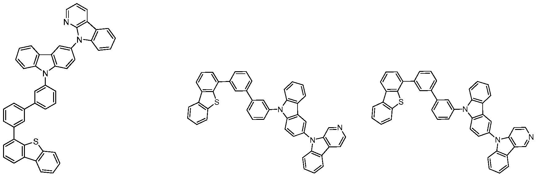
[0060] In one embodiment, the first organic layer is an emissive layer and the compound of formula I is a host. In another embodiment, the device further comprises a second organic layer that is a non-emissive layer and the compound having formula I is a material in the second organic layer. In one embodiment, the organic layer further comprises an emissive compound. The emissive compound is preferably a transition metal complex having at least one ligand selected from the group consisting of:
Without being bound by theory, incorporating these transition metal ligands into OLED devices enables the manufacture of OLED devices with highly desirable properties, e.g. high efficiency, long triplet lifetimes, etc.
[0061] In one embodiment, Ra, Rb, and Rc independently represent mono, di, tri or tetra substitutions. In another embodiment, Ra, Rb, and Rc are independently selected from the group consisting of hydrogen, deuterium, halide, alkyl, cycloalkyl, heteroalkyl, arylalkyl, alkoxy, aryloxy, amino, silyl, alkenyl, cycloalkenyl, heteroalkenyl, alkynyl, aryl, heteroaryl, acyl, carbonyl, carboxylic acids, ester, nitrile, isonitrile, sulfanyl, sulfmyl, sulfonyl, phosphino, and combinations thereof. In one embodiment two adjacent substituents of Ra, Rb, and Rc are optionally joined to form a fused ring.
[0062] In one embodiment, the second organic layer is an electron transporting layer and the compound having the formula I is an electron transporting material in the second organic layer. In another embodiment, the second organic layer is a blocking layer and the compound having the formula I is a blocking material in the second organic layer. As described below, the use of compounds of formula I in OLED devices is advantageous because of their desirable properties, e.g. quantum efficiency, luminance, etc.
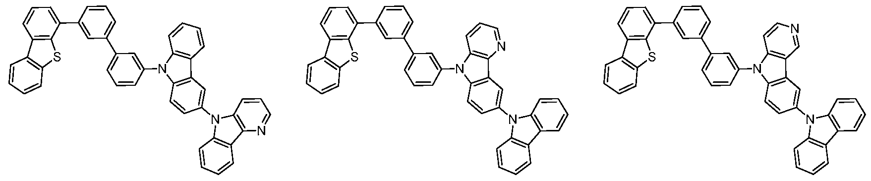
[0063] An exemplary OLED device incorporating the novel compounds described herein as well as comparative compounds is depicted in FIG. 4. The OLED device was made with vacuum thermal deposition techniques known to those of skill in the art. [0064] The components of the OLED device in FIG. 4 are as follows: 800 A of ITO surface electrode, 100 A of Compound HIL as the hole injection layer, 300 A of Compound NPD as the hole transporting layer (HTL), 300 A of Compound 1 (Cmpd. 1) or Comparison Compound (Comp. Cmpd.) doped with 15 wt% of Dopant Compound as the emissive layer (EML), 50 A of Compound 1 or Compound BL as the blocking layer, and 400 A of Alq
3 as the ETL. [0065] The structures of the OLED layer components are as follows:
[0066] Table 1 lists the results obtained using novel Compound 1 compared to Comparison Compound in an OLED device.
TABLE 1
[0067] The OLED device in Example 1 and Comparative Example 1 in Table 1 have the same structure except in the first case Compound 1 was used as the host, while in the second case Comparison Compound was used as the host. In both cases Compound BL was used as a blocking layer. It is readily apparent from Table 1, that Compound 1 provided better luminance efficiency (LE), external quantum efficiency (EQE), and power efficiency (PE) and significantly better device lifetime than the Comparison Compound. LTgo is defined as the time required for the initial luminance, L
0, to drop from 100% to 80% under constant current density at room temperature. Similar results were observed when Compound 1 and the Comparison Compound were used in the blocking layer instead of as hosts. In all cases, the use of Compound 1 provided devices with greater efficiencies and lifetimes than the Comparison Compound.
[0068] The data suggests that use of compounds of formula I, which contain an
oligoazacarbazole and dibenzothiophene or dibenzofuran moieties linked by an aromatic spacer, as the blocking layer or the host, result in higher device stability compared to compounds with a single azacarbazole moiety and dibenzothiophene moiety (i.e. the Comparison Compound). Oligoazacarbazole, the main HOMO contributor in compounds of formula I, is more electron rich than azacarbazole. Compounds of formula I, such as Compound 1, are superior to compounds similar to the Comparison Compound because the higher HOMO level of compounds of formula I can increase hole injection from the HTL and hole transport in the EML. These properties of compounds of formula I can result in better device charge balance and/or location of charge recombination, leading to improved device lifetime.
[0069] The materials described herein as useful for a particular layer in an organic light emitting device may be used in combination with a wide variety of other materials present in the device. For example, emissive dopants disclosed herein may be used in conjunction with a wide variety of hosts, transport layers, blocking layers, injection layers, electrodes and other layers that may be present. The materials described or referred to below are non-limiting examples of materials that may be useful in combination with the compounds disclosed herein, and one of skill in the art can readily consult the literature to identify other materials that may be useful in combination.
[0070] In addition to and / or in combination with the materials disclosed herein, many hole injection materials, hole transporting materials, host materials, dopant materials, exiton/hole
blocking layer materials, electron transporting and electron injecting materials may be used in an OLED. Non- limiting examples of the materials that may be used in an OLED in combination with materials disclosed herein are listed below. The list includes non-limiting classes of materials, non-limiting examples of compounds for each class, and references that disclose the materials.
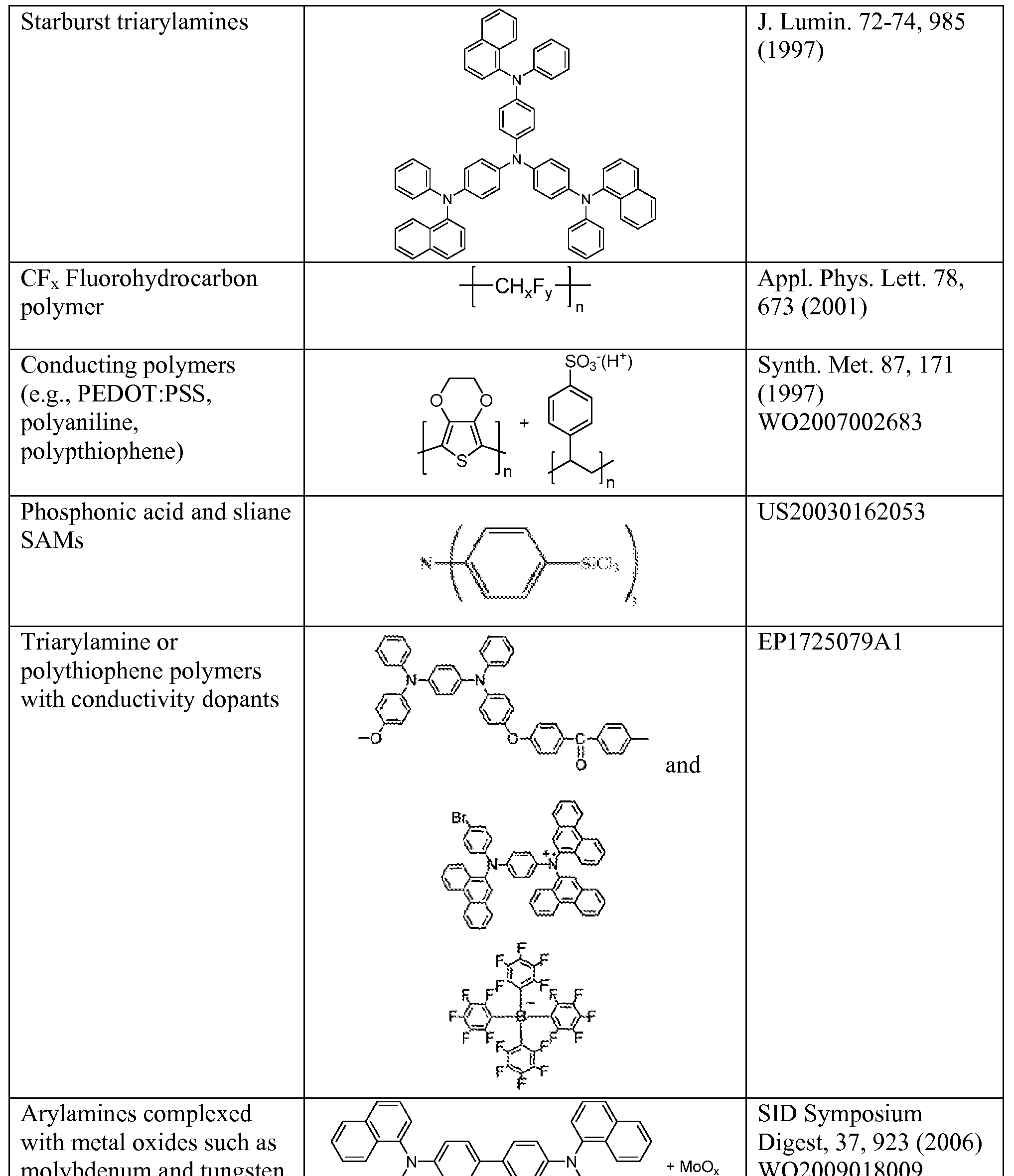
HIL/HTL:
[0071] A hole injecting/transporting material to be used in the present invention is not particularly limited, and any compound may be used as long as the compound is typically used as a hole injecting/transporting material. Examples of the material include, but not limit to: a phthalocyanine or porphryin derivative; an aromatic amine derivative; an indolocarbazole derivative; a polymer containing fluorohydrocarbon; a polymer with conductivity dopants; a conducting polymer, such as PEDOT/PSS; a self-assembly monomer derived from compounds such as phosphonic acid and sliane derivatives; a metal oxide derivative, such as MoOx; a p-type semiconducting organic compound, such as 1,4,5,8,9,12-Hexaazatriphenylenehexacarbonitrile; a metal complex, and a cross-linkable compounds.
[0072] Examples of aromatic amine derivatives used in HIL or HTL include, but not limit to the following general structures:
Ar2. Ar3
N
Ar1 Ar\ /Af4 Ar4^ ^Ar^ ^Ar7
I N— Ar1— N I N
/ N . / \ I
Ar2 ^Ar3 Ar3 Ar5 Ar5 Ar6
[0073] Each of Ar1 to Ar9 is selected from the group consisting aromatic hydrocarbon cyclic compounds such as benzene, biphenyl, triphenyl, triphenylene, naphthalene, anthracene,
phenalene, phenanthrene, fluorene, pyrene, chrysene, perylene, azulene; group consisting aromatic heterocyclic compounds such as dibenzothiophene, dibenzofuran, dibenzoselenophene, furan, thiophene, benzofuran, benzothiophene, benzoselenophene, carbazole, indolocarbazole, pyridylindole, pyrrolodipyridine, pyrazole, imidazole, triazole, oxazole, thiazole, oxadiazole, oxatriazole, dioxazole, thiadiazole, pyridine, pyridazine, pyrimidine, pyrazine, triazine, oxazine, oxathiazine, oxadiazine, indole, benzimidazole, indazole, indoxazine, benzoxazole,
benzisoxazole, benzothiazole, quinoline, isoquinoline, cinnoline, quinazoline, quinoxaline, naphthyridine, phthalazine, pteridine, xanthene, acridine, phenazine, phenothiazine,
phenoxazine, benzofuropyridine, furodipyridine, benzothienopyridine, thienodipyridine, benzoselenophenopyridine, and selenophenodipyridine; and group consisting 2 to 10 cyclic structural units which are groups of the same type or different types selected from the aromatic hydrocarbon cyclic group and the aromatic heterocyclic group and are bonded to each other directly or via at least one of oxygen atom, nitrogen atom, sulfur atom, silicon atom, phosphorus atom, boron atom, chain structural unit and the aliphatic cyclic group. Wherein each Ar is further substituted by a substituent selected from the group consisting of hydrogen, deuterium, halide, alkyl, cycloalkyl, heteroalkyl, arylalkyl, alkoxy, aryloxy, amino, silyl, alkenyl, cycloalkenyl, heteroalkenyl, alkynyl, aryl, heteroaryl, acyl, carbonyl, carboxylic acids, ester, nitrile, isonitrile, sulfanyl, sulfinyl, sulfonyl, phosphino, and combinations thereof.
[0074] In one aspect, Ar1 to Ar9 is independently selected from the group consisting of:
[0075] k is an integer from 1 to 20; X1 to X8 is CH or N; Ar1 has the same group defined above.
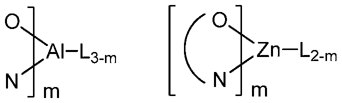
[0076] Examples of metal complexes used in HIL or HTL include, but not limit to the following general formula:
[0077] M is a metal, having an atomic weight greater than 40; (Y^Y2) is a bindentate ligand, Yl and Y2 are independently selected from C, N, O, P, and S; L is an ancillary ligand; m is an integer value from 1 to the maximum number of ligands that may be attached to the metal; and m+n is the maximum number of ligands that may be attached to the metal.
[0078] In one aspect, (Y^Y2) is a 2-phenylpyridine derivative.
[0079] In another aspect, (Y^Y2) is a carbene ligand.
[0080] In another aspect, M is selected from Ir, Pt, Os, and Zn.
[0081] In a further aspect, the metal complex has a smallest oxidation potential in solution vs. Fc+/Fc couple less than about 0.6 V.
Host:
[0082] The light emitting layer of the organic EL device of the present invention preferably contains at least a metal complex as light emitting material, and may contain a host material using the metal complex as a dopant material. Examples of the host material are not particularly limited, and any metal complexes or organic compounds may be used as long as the triplet energy of the host is larger than that of the dopant.
[0083] Examples of metal complexes used as host are preferred to have the following general formula:
[0084] M is a metal; (Y
3-Y
4) is a bindentate ligand, Y
3 and Y
4 are independently selected from C, N, O, P, and S; L is an ancillary ligand; m is an integer value from 1 to the maximum number of ligands that may be attached to the metal; and m+n is the maximum number of ligands that may be attached to the metal.
[0085] In one aspect, the metal complexes
[0086] (O-N) is a bidentate ligand, having metal coordinated to atoms O and N.
[0087] In another aspect, M is selected from Ir and Pt. [0088] In a further aspect, (Y3-Y4) is a carbene ligand.
[0089] Examples of organic compounds used as host are selected from the group consisting aromatic hydrocarbon cyclic compounds such as benzene, biphenyl, triphenyl, triphenylene, naphthalene, anthracene, phenalene, phenanthrene, fluorene, pyrene, chrysene, perylene, azulene; group consisting aromatic heterocyclic compounds such as dibenzothiophene, dibenzofuran, dibenzoselenophene, furan, thiophene, benzofuran, benzothiophene, benzoselenophene, carbazole, indolocarbazole, pyridylindole, pyrrolodipyridine, pyrazole, imidazole, triazole, oxazole, thiazole, oxadiazole, oxatriazole, dioxazole, thiadiazole, pyridine, pyridazine, pyrimidine, pyrazine, triazine, oxazine, oxathiazine, oxadiazine, indole, benzimidazole, indazole, indoxazine, benzoxazole, benzisoxazole, benzothiazole, quinoline, isoquinoline, cinnoline, quinazoline, quinoxaline, naphthyridine, phthalazine, pteridine, xanthene, acridine, phenazine, phenothiazine, phenoxazine, benzofuropyridine, furodipyridine, benzothienopyridine, thienodipyridine, benzoselenophenopyridine, and selenophenodipyridine; and group consisting 2 to 10 cyclic structural units which are groups of the same type or different types selected from the aromatic hydrocarbon cyclic group and the aromatic heterocyclic group and are bonded to each other directly or via at least one of oxygen atom, nitrogen atome, sulfur atom, silicon atom, phosphorus atom, boron atom, chain structural unit and the aliphatic cyclic group. Wherein each group is further substituted by a substituent selected from the group consisting of hydrogen, deuterium, halide, alkyl, cycloalkyl, heteroalkyl, arylalkyl, alkoxy, aryloxy, amino, silyl, alkenyl, cycloalkenyl, heteroalkenyl, alkynyl, aryl, heteroaryl, acyl, carbonyl, carboxylic acids, ester, nitrile, isonitrile, sulfanyl, sulfinyl, sulfonyl, phosphino, and combinations thereof.
[0090] In one aspect, host compound contains at least one of the following groups in the molecule:
[0091] R1 to R7 is independently selected from the group consisting of hydrogen, alkyl, alkoxy, amino, alkenyl, alkynyl, arylalkyl, heteroalkyl, aryl and heteroaryl, when it is aryl or heteroaryl, it has the similar definition as Ar's mentioned above. [0092] k is an integer from 0 to 20.
[0093] X1 to X8 is selected from CH or N.
HBL:
[0094] A hole blocking layer (HBL) may be used to reduce the number of holes and/or excitons that leave the emissive layer. The presence of such a blocking layer in a device may result in substantially higher efficiencies as compared to a similar device lacking a blocking layer. Also, a blocking layer may be used to confine emission to a desired region of an OLED.
[0095] In one aspect, compound used in HBL contains the same molecule used as host described above.
[0096] In another aspect, compound used in HBL contains at least one of the following groups in the molecule:
[0097] k is an integer from 0 to 20; L is an ancillary ligand, m is an integer from 1 to 3. ETL:
[0098] Electron transport layer (ETL) may include a material capable of transporting electrons. Electron transport layer may be intrinsic (undoped), or doped. Doping may be used to enhance conductivity. Examples of the ETL material are not particularly limited, and any metal complexes or organic compounds may be used as long as they are typically used to transport electrons.
[0099] In one aspect, compound used in ETL contains at least one of the following groups in the molecule:
[0100] R1 is selected from the group consisting of hydrogen, deuterium, halide, alkyl, cycloalkyl, heteroalkyl, arylalkyl, alkoxy, aryloxy, amino, silyl, alkenyl, cycloalkenyl, heteroalkenyl, alkynyl, aryl, heteroaryl, acyl, carbonyl, carboxylic acids, ester, nitrile, isonitrile, sulfanyl, sulfmyl, sulfonyl, phosphino, and combinations thereof, when it is aryl or heteroaryl, it has the similar definition as Ar's mentioned above.
[0101] Ar1 to Ar3 has the similar definition as Ar's mentioned above. [0102] k is an integer from 0 to 20. [0103] X1 to X8 is selected from CH or N.
[0104] In another aspect, the metal complexes used in ETL contains, but not limit to the following general formula:
[0105] (O-N) or (N-N) is a bidentate ligand, having metal coordinated to atoms O, N or N, N; L is an ancillary ligand; m is an integer value from 1 to the maximum number of ligands that may be attached to the metal.
[0106] In any above-mentioned compounds used in each layer of the OLED device, the hydrogen atoms can be partially or fully deuterated.
[0107] In addition to and / or in combination with the materials disclosed herein, many hole injection materials, hole transporting materials, host materials, dopant materials, exiton/hole blocking layer materials, electron transporting and electron injecting materials may be used in an OLED. Non- limiting examples of the materials that may be used in an OLED in combination with materials disclosed herein are listed in Table 2 below. Table 2 lists non-limiting classes of materials, non-limiting examples of compounds for each class, and references that disclose the materials.
Anthracene- WO2003060956 benzoimidazole
compounds X) Q-n
US20090179554
Aza triphenylene US20090115316 derivatives
Anthracene-benzothiazole Appl. Phys. Lett. 89, compounds XXK>$-CHXX 063504 (2006)
Metal 8-hydroxyquinolates Appl. Phys. Lett. 51, (e.g., Alq3, Zrq4) 913 (1987)
3 US7230107
Metal Chem. Lett. 5, 905 hydroxybenoquinolates (1993)
2
Bathocuprine compounds Appl. Phys. Lett. 91, such as BCP, BPhen, etc 263503 (2007)
Appl. Phys. Lett. 79, 449 (2001)
[0108] It is understood that the various embodiments described herein are by way of example only, and are not intended to limit the scope of the invention. For example, many of the materials and structures described herein may be substituted with other materials and structures without deviating from the spirit of the invention. The present invention as claimed may therefore includes variations from the particular examples and preferred embodiments described herein, as will be apparent to one of skill in the art. It is understood that various theories as to why the invention works are not intended to be limiting.
Examples [0109] Chemical abbreviations used throughout this document are as follows: PPh3 is triphenylphosphine, DCM is dichloromethane, dba is dibenzylideneacetone, Cy is cyclohexyl, OAc is acetate, DBU is l,8-diazabicyclo[5.4.0]undec-7-ene, dppf is Ι,Γ- bis(diphenylphosphino)ferrocene, THF is tetrahydrofuran.
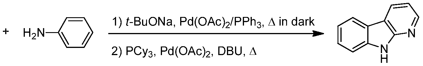
[0110] Synthesis of Compound 1 Step 1 a CI
N CI
[0111] Into a mixture of sodium tert-butoxide (11.69 g, 122 mmol), triphenylphosphine (2.66 g, 10.14 mmol), palladium acetate (1.138 g, 5.07 mmol), 2,3-dichloropyridine (15 g, 101 mmol) and aniline (10.18 ml, 111 mmol) was added o-xylene (100 mL). The solution was degased by vacuum-nitrogen cycles before heating at 120 °C in the absence of light for 3 hours and cooled to room temperature. In another flask, tricyclohexylphosphine (16.04 ml, 10.14 mmol), palladium acetate (1.138 g, 5.07 mmol), and DBU (30.6 ml, 203 mmol) were dissolved in
dimethylacetamide (100 ml). This solution was degassed by vacuum/nitrogen cycles and transferred to the above reaction mixture. The resultant reaction mixture was stirred at 150 °C for another 12 hours, cooled to room temperature and quenched with water. The aqueous phase was extracted with ethyl acetate. The combined organic phase was washed with aqueous LiCl (10 wt%) solution, dried over MgSC^. Upon evaporation off the solvent, the black residue was precipitated from dichloromethane into hexane. The crude product was purified by
recrystallization from toluene to yield 9H-pyrido[2,3-b]indole as a yellowish white product (9.0 g).
Step 2
mL flask was added 9H-pyrido[2,3-b]indole (5 g, 29.7 mmol), N-tosyl-3-iodocarbazole (14.63 g, 32.7 mmol), copper(I) iodide (0.283 g, 1.486 mmol) and potassium phosphate (13.25 g, 62.4 mmol). It was degassed before the addition of anhydrous m-xylene (150 mL) and cyclohexane 1,2-diamine (0.339 g, 2.97 mmol). The resultant green suspension was refluxed for three days Column chromatography on silica gel (eluent hexane/DCM 1 :4, v/v) provided the product 9-(9 tosyl-carbazol-3-yl)-pyrido[2,3-b]indole (9.9 g).
Step 3
[0113] A mixture solution of 9-(9-tosyl-carbazol-3-yl)-pyrido[2,3-b]indole (9.9g, 20.30 mmo and NaOH (8.12g, 203mmol) in THF (100 mL), ethanol (50 mL) and water (50 mL) was refluxed over weekend. After cooling to room temperature, the white solid was obtained by filtration, and washed successively with water, ethanol, DCM and ethanol to yield the 9-(9H- carbazol-3-yl)-9H-pyrido[2,3-b]indole (4.8 g).
[0114] Synthesis of 4-(3'-bromo-[l,l'-biphenyl]-3-yl)(iibenzo[b,(i]thiophene.
1. Synthesis of 4-(3-bromophenyl)dibenzo[b,d]thiophene
[0115] Dibenzo[b,d]thiophen-4-yl-boronic acid (10.00 g, 43.8 mmol), 1,3-dibromobenzene (20.69 g, 88 mmol) and Pd(PPh3)4 catalyst (0.507 g, 0.438 mmol) were dissolved in 200 mL of toluene, and potassium carbonate (18.18 g, 132 mmol) in 50 mL of water was added, and the mixture was refiuxed overnight under N2. The mixture was cooled to room temperature, and the organic layer was separated, filtered and evaporated. The residue after evaporation was purified by column chromatography on silica gel (eluted with hexane/DCM 95/5 v/v mixture), followed by recrystallization from hexane. 4-(3-bromophenyl)dibenzo[b,d]thiophene was obtained as white solid (12 g, 81% yield).
2. Synthesis of 2-(3-(dibenzo[b,d]thiophen-4-yl)phenyl)-4,4,5,5-tetramethyl-l,3,2-dioxaborolane
[0116] 4-(3-bromophenyl)dibenzo[b,d]thiophene (18.50 g, 54.5 mmol) and 4,4,4*,4*,5,5,5*,5*- octamethyl-2,2'-bi(l,3,2-dioxaborolane) (18.00 g, 70.9 mmol) were dissolved in 200 mL of dioxane, and to the dioxane solution potassium acetate (10.70 g, 109 mmol), Ι,Γ- bis(diphenylphosphino) ferrocene (0.666 g, 1.091 mmol) and
tris(dibenzylideneacetone)dipalladium(0) (0.499 g, 0.545 mmol) were added. The reaction mixture was degassed and heated to reflux overnight, cooled down to room temperature, filtered and evaporated. Column chromatography on silica gel with hexane/DCM 95/5 v/v eluent provided 2-(3-(dibenzo[b,d]thiophen-4-yl)phenyl)-4,4,5,5-tetramethyl-l,3,2-dioxaborolane as white solid (15.1 g, 71%).
3. Synthesis of 4-(3'-bromo-[l,l'-biphenyl]-3-yl)dibenzo[b,d]thiophene
[0117] 2 3-(dibenzo[b,d]thiophen-4-yl)phenyl)-4,4,5,5-tetramethyl-l,3,2-dioxaborolane (8.80 g, 22.78 mmol) and 1,3-dibromobenzene (21.49 g, 91 mmol) were dissolved in toluene (300 mL), and potassium carbonate (9.44 g, 68.3 mmol) in 50 mL of water and the Pd(PPh3)4 catalyst (0.263 g, 0.228 mmol) were then added. The reaction mixture was degassed and refluxed under N2 overnight. The organic layer was then separated, evaporated and subjected to column chromatography on silica gel, eluted with hexane/DCM 9: 1 v/v mixture, providing 4-(3'-bromo- [l,l'-biphenyl]-3-yl)dibenzo[b,d]thiophene (7.5 g, 18.06 mmol, 79 % yield) as white solid. tep 4
[0118] A solution of 9-(9H-carbazol-3-yl)-pyrido[2,3-b]indole (2.50 g, 7.50 mmol), 4-(3*- bromo-[l,l'-biphenyl]-3-yl)dibenzo[b,d]thiophene (3.11 g, 7.50 mmol), Pd2(dba)3 (0.137 g, 0.150 mmol), dicyclohexyl(2',6'-dimethoxy-[l, -biphenyl]-3-yl)phosphine (0.123 g, 0.30 mmol), and sodium tert-butoxide (1.44 g, 15.00 mmol) in xylene (150 mL) was refluxed in nitrogen overnight. After cooling to room temperature, the reaction mixture was washed with water, dried over Na2S04 and the solvent was evaporated. The residue was dissolved in hot toluene, mixed with celite, and purified by column chromatography with hexane toluene (1 :9 to 0: 10, v/v) as eluent. The product was precipitated in ethanol, and further purified by thermal sublimation under vacuum (<105 torr ) to yield 9-(9-(3*-(dibenzo[b,d]thiophen-4-yl)-[l,r-biphenyl]-3-yl)- carbazol-3-yl)-pyrido[2,3-b]indole as a white glassy solid (3.21 g).