WO2011105408A1 - Simd processor - Google Patents
Simd processor Download PDFInfo
- Publication number
- WO2011105408A1 WO2011105408A1 PCT/JP2011/053935 JP2011053935W WO2011105408A1 WO 2011105408 A1 WO2011105408 A1 WO 2011105408A1 JP 2011053935 W JP2011053935 W JP 2011053935W WO 2011105408 A1 WO2011105408 A1 WO 2011105408A1
- Authority
- WO
- WIPO (PCT)
- Prior art keywords
- instruction
- pes
- simd
- simd processor
- data
- Prior art date
Links
- 238000012545 processing Methods 0.000 claims abstract description 16
- 238000012546 transfer Methods 0.000 claims description 7
- 239000013256 coordination polymer Substances 0.000 claims 7
- 238000000034 method Methods 0.000 description 10
- 230000000694 effects Effects 0.000 description 7
- 238000011161 development Methods 0.000 description 6
- 238000010586 diagram Methods 0.000 description 5
- 101100243454 Caenorhabditis elegans pes-10 gene Proteins 0.000 description 4
- 101100136062 Mycobacterium tuberculosis (strain ATCC 25618 / H37Rv) PE10 gene Proteins 0.000 description 4
- 230000008859 change Effects 0.000 description 4
- 230000008569 process Effects 0.000 description 3
- 238000004364 calculation method Methods 0.000 description 2
- 230000008878 coupling Effects 0.000 description 2
- 238000010168 coupling process Methods 0.000 description 2
- 238000005859 coupling reaction Methods 0.000 description 2
- 230000006872 improvement Effects 0.000 description 2
- 101000741396 Chlamydia muridarum (strain MoPn / Nigg) Probable oxidoreductase TC_0900 Proteins 0.000 description 1
- 101000741399 Chlamydia pneumoniae Probable oxidoreductase CPn_0761/CP_1111/CPj0761/CpB0789 Proteins 0.000 description 1
- 101000741400 Chlamydia trachomatis (strain D/UW-3/Cx) Probable oxidoreductase CT_610 Proteins 0.000 description 1
- 101100136063 Mycobacterium tuberculosis (strain ATCC 25618 / H37Rv) PE11 gene Proteins 0.000 description 1
- 230000004913 activation Effects 0.000 description 1
- 230000002457 bidirectional effect Effects 0.000 description 1
- 230000006870 function Effects 0.000 description 1
- 238000013507 mapping Methods 0.000 description 1
- 230000007246 mechanism Effects 0.000 description 1
- 238000012986 modification Methods 0.000 description 1
- 230000004048 modification Effects 0.000 description 1
Images

Classifications
-
- G—PHYSICS
- G06—COMPUTING; CALCULATING OR COUNTING
- G06F—ELECTRIC DIGITAL DATA PROCESSING
- G06F15/00—Digital computers in general; Data processing equipment in general
- G06F15/76—Architectures of general purpose stored program computers
- G06F15/80—Architectures of general purpose stored program computers comprising an array of processing units with common control, e.g. single instruction multiple data processors
- G06F15/8007—Architectures of general purpose stored program computers comprising an array of processing units with common control, e.g. single instruction multiple data processors single instruction multiple data [SIMD] multiprocessors
-
- G—PHYSICS
- G06—COMPUTING; CALCULATING OR COUNTING
- G06F—ELECTRIC DIGITAL DATA PROCESSING
- G06F9/00—Arrangements for program control, e.g. control units
- G06F9/06—Arrangements for program control, e.g. control units using stored programs, i.e. using an internal store of processing equipment to receive or retain programs
- G06F9/30—Arrangements for executing machine instructions, e.g. instruction decode
- G06F9/38—Concurrent instruction execution, e.g. pipeline, look ahead
- G06F9/3885—Concurrent instruction execution, e.g. pipeline, look ahead using a plurality of independent parallel functional units
- G06F9/3887—Concurrent instruction execution, e.g. pipeline, look ahead using a plurality of independent parallel functional units controlled by a single instruction for multiple data lanes [SIMD]
Definitions
- the present invention relates to a SIMD (Single Instruction Multiple Data) processor.
- SIMD Single Instruction Multiple Data
- FIG. 9 is a diagram showing the configuration of the SIMD processor described in Non-Patent Document 1.
- the SIMD processor includes a plurality of computing elements (PE: Processing Element) 110 and a control processor (CP: Control Processor) 130 that issues the same instruction to the plurality of PEs 110.
- PE Processing Element
- CP Control Processor
- high computing performance can be realized based on inexpensive hardware.
- the data arranged at a predetermined position on the global memory (Global Memory) 140 managed by the CP 130 is sequentially read into the local memory (Local Memory) 120 on the PE 110 side in the order of addresses. Thereafter, all the PEs 110 perform calculations on the data in their local memory 120 at the same time in accordance with instructions issued from the CP 130.
- Patent Document 1 describes an image processor that can switch between a SIMD type and a systolic array type configuration.
- a dynamically reconfigurable processor As described above, a method of connecting a large number of memory blocks and a large number of PEs with abundant wiring (for example, crossbars) can be considered. However, according to this method, since it is necessary to add a large number of wiring circuits to the SIMD processor, hardware for realizing the SIMD processor becomes expensive.
- An object of the present invention is to provide a SIMD processor that solves such problems.
- the SIMD processor is: A SIMD (Single Instruction Multiple Data) processor comprising a control processor (CP: Control Processor) and a plurality of computing elements (PE: Processing Element), The plurality of PEs perform a SIMD operation to execute a single instruction issued from the CP, The CP performs a command / data distribution operation for distributing different commands or different commands and data to each of the plurality of PEs, Each of the plurality of PEs performs a systolic operation of executing an instruction sent from the CP in the instruction / data distribution operation after the source operands of the instruction are prepared.
- CP Control Processor
- PE Processing Element
- the SIMD processor According to the SIMD processor according to the present invention, it is possible to process a program at high speed by utilizing the arithmetic elements of the SIMD processor without changing the data arrangement on the global memory.
- the SIMD processor according to the first viewpoint is provided.
- the CP is provided with a SIMD processor that sequentially and exclusively uses instruction issue paths for all PEs in order to distribute instructions to each PE in the instruction / data distribution operation.
- the plurality of PEs transfer the operation results of the executed operation instructions to other PEs, and the operation results transferred from the other PEs are
- a SIMD processor is provided that serves as a source operand for instructions sent in an instruction / data distribution operation.
- each of the plurality of PEs uses the data sent from the CP as a source operand for the instruction sent in the command / data distribution operation. Is provided.
- a global access arbitration unit (Global Access Arbiter) that arbitrates global memory access by each of the plurality of PEs and guarantees access exclusiveness to the global memory is further provided.
- a SIMD processor is provided.
- a SIMD processor in which each of the plurality of PEs includes a register for storing a flag for keeping the operation stopped during the instruction / data distribution operation.
- a SIMD processor in which each of the plurality of PEs includes a register that stores a flag for switching the operation between the SIMD operation and the systolic operation.
- a SIMD processor in which each of the plurality of PEs includes a selector that selects whether or not to store an instruction issued from the CP in its own instruction buffer.
- the SIMD processor performs SIMD operation in which the entire PE array executes a single instruction issued from the control processor (CP), and the CP uses the instruction issue path to transmit different instruction codes and data.
- the instruction / data distribution operation to be sequentially transmitted to each PE is performed, and each PE in the PE array receives the instruction transmitted from the CP by the instruction / data distribution operation, not the instruction broadcast from the CP every cycle.
- a systolic operation is performed to specify that the execution result of the instruction is written to the register resource of another designated PE.
- each PE starts executing the instruction after the operands of the instruction are written by data sent from other PEs or CPs. It is sent to another PE, and in the case of a memory access command, the global memory is accessed.
- the SIMD processor of the present invention different instructions can be issued to each PE by the instruction / data distribution operation. Accordingly, it is possible to shift the timing of executing the memory access instruction between the PEs, or to allow only a specific PE to execute the memory access instruction. At this time, even if the data arrangement on the memory is left as it is and the memory space accessible by the PE is expanded to the global memory space, there are a number of cases when using the global memory space that is a single hardware resource. The frequency of competing PEs can be reduced, and the processing performance of the processing resources of the processor can be improved.
- the SIMD processor according to the present invention it is possible to speed up the processing using the operation resource of the SIMD processor without changing the data arrangement on the memory of the program (first effect).
- the CP performs an instruction / data distribution operation on the PE array, so that each arithmetic instruction corresponding to each arithmetic node and related constant data when processing for one iteration is expressed as a data flow graph It is possible to distribute to each PE and assign each operation node in the data flow graph to each PE. Further, in order for the CP to start execution in the systolic operation mode in the PE array, the activation data is repeatedly issued to one or more PEs, thereby starting up the different iterations one after another. The array can be processed.
- the processing for the portion (parallel loop portion) having no data dependency among the iterations in the loop portion of the program can be performed without changing the data arrangement on the global memory.
- the speed can be increased (second effect).
- the circuit resources of the instruction issue path to all PEs provided in the conventional SIMD processor and the data wiring circuit resources from each PE to the CP and from the CP to each PE are allocated. It can be used as it is. Further, as a connection for accessing the global memory space from each PE, a wiring circuit resource for exchanging scalar data between a CP and a PE array provided in a conventional SIMD processor can be used as it is. Furthermore, between PEs that perform operations in which operation nodes on the data flow graph transmit / receive data to / from each other, as a connection between PEs for transmitting / receiving data, the wiring resources between adjacent PEs provided in the conventional SIMD processor are used as they are. Can be used.
- the first effect and the second effect can be obtained (third effect) only by adding a small amount of circuit to the conventional SIMD processor.
- FIG. 10 is a diagram showing a configuration of one PE 110 in a PE array included in a conventional SIMD processor.
- the PE 110 stores an instruction buffer (instb) 111 for storing instructions issued from the CP 130 (FIG. 9), general purpose registers (General Purpose Registers) r0 to r7, and arithmetic units (ALU: Arithmetic Logic Unit). ) 112, and an entry / exit to the connection network between PEs (Left / Right Inter PE Connection), and a local memory 120 for each PE (Local Memory). All the PEs 110 simultaneously execute a single instruction issued from the CP 130 every cycle.
- instruction buffer instb
- general purpose registers General Purpose Registers
- ALU Arithmetic Logic Unit
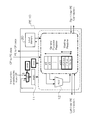
- FIG. 1 shows a configuration of 1 PE 10 in a PE array included in a SIMD processor according to this embodiment.
- the PE 10 includes an instruction buffer (instb) 11, general purpose registers (General Purpose Registers) r 0 to r 15, an arithmetic unit (ALU: Arithmetic Logic Unit) 12, and an entrance / exit to a connection network between PEs (Left / Right Interchange). PE Connection) and local memory 20 for each PE.
- the PE 10 further includes registers stop and mode and a selector sel.
- FIG. 1 components (thick line portions) added to FIG. 10, that is, registers stop, mode, selector sel, registers cm, sx, and sy will be described.
- the register stop is a control register for keeping the operation of the PE 10 stopped during the instruction / data distribution operation.
- the register mode is a 1-bit operation mode selection register for switching between a systolic operation and a conventional SIMD operation.
- the selector sel is a selector that selects whether or not an instruction issued from the CP is stored in the instruction buffer (instb) 11.
- the registers cm, sx, and sy are a general-purpose register (waiting register) group having a data waiting function in which a predetermined counter register is decremented each time a write to the register occurs during a systolic operation.
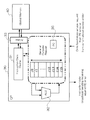
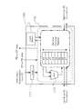
- FIG. 2 is a diagram schematically showing the configuration of the control processor (CP) 30 included in the SIMD processor according to the present embodiment.
- CP 30 has a data path for performing its own operation, and is an instruction / data cache (Instruction / Data Cache) 31, and a memory access adjustment unit, like CP 130 in the conventional SIMD processor. It is connected to a global memory 40 via an arbiter 33.
- the CP 30 reads and issues commands to be executed in its own data path and commands to be broadcast to the entire PE array from the global memory 40, and is transmitted and received between the calculation data on the CP 30 and the local memory 20 of the PE 10. Data to be read from the global memory 40 or written to the global memory 40.
- FIG. 3 is a diagram illustrating an example of an instruction format in the SIMD processor according to the present embodiment.
- the CP 30 in the SIMD processor of the present embodiment is different from the CP 130 in the conventional SIMD processor, and sends instructions and / or data to a specific PE at the same time and executes them to a specific PE or a plurality of designated PEs.
- An instruction set having an instruction format as shown in FIG. 3 is used.
- the instruction format of CP30 has a different format according to the bit pattern of the header section of the instruction.
- the bit pattern of the “header” part is “10”, it indicates that the instruction A is to be distributed to the specific PE 10, and as a subsequent instruction, an instruction B whose bit pattern of the header part is always “11”
- the instruction A is written to the instruction buffer (instb) 11 of the PE of the PE number indicated by the “Target PEID” part of the instruction B, and the PE register of the PE number indicated by the “Target reg ID” part of the instruction B is written. Specifies the operation of writing the “data” part of the instruction B.
- the value of the “data” part is stored in the register of the number indicated by the “Target reg ID” part of the PE of the PE number indicated by the “Target PEID” part of the instruction.
- the instruction stored in the instruction buffer (instb) 11 writes the value of the data part to the register cm of the PE 10 having cm as the source operand. specify.
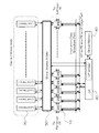
- FIG. 4 shows the overall configuration of the PE array in the SIMD processor according to this embodiment.
- the bold line portion indicates a global access arbitration unit (Global Access Arbiter) 50, which is a circuit element newly added in the present invention, in addition to the individual PEs 10, with respect to the conventional SIMD processor.
- Global Access Arbiter Global Access Arbiter
- the global access arbitration unit 50 is a module that manages the local memory blocks of all the PEs 20 so that they can be used together as a multi-bank cache memory body, and memory access is simultaneously generated from a large number of PEs 10 during the systolic operation mode. If this occurs, the memory access is arbitrated.
- the following method can be considered. In other words, when there are memory access requests from two or more PEs simultaneously, the operation of the entire PE array is temporarily stopped, the memory access requests of each PE are answered one by one, and then the operation of the PE array is resumed.
- An implementation method with low performance but low hardware implementation cost is conceivable.
- a mounting method that has the highest performance but high hardware implementation cost is conceivable, in which local memory blocks of all PEs are connected by a crossbar mechanism to respond to a large number of memory access requests with the shortest possible delay. Any mounting method may be adopted as long as the maximum memory access delay can be determined statically when arbitrary program code is executed in a superimposed manner.
- the CP 30 simultaneously reads two instructions, the instruction at the address indicated by the value of the program counter (PC: Program Counter) 35 and the instruction at the next address. However, whether the count value of the PC 35 is incremented or decremented every cycle and how the read instruction is processed is determined by “header” of the read first instruction A. It is determined as follows according to the value of the part.
- PC Program Counter
- an instruction having a “header” value of “10” includes a “counter” portion. It is assumed that a value equal to or greater than the number of “waiting registers” among the source operands of the instruction is set in the “counter” portion.
- the PE number specified by the “target PEID” portion of the instruction A is on the PE.
- a write operation P is performed on the register sx.
- the value “1” is set in the “counter” portion of the instruction C in the instruction buffer (instb) 11 of the PE, and the register sx is the only “waiting register” in the source operand of the instruction C.
- the “counter” part of the instruction C includes The value 1 is set again.
- the “counter” portion is not 1 but 0 which is the decrement result. Since it is set, the instruction C is continuously executed on the PE.
- CP30 executes an instruction A in which the waiting register cm is specified in the “Target reg ID” part in the systolic operation, all having cm as a source operand in the instruction buffer (instb) 11
- the writing operation P to cm occurs with respect to the PE.
- the value “2” is set in the “counter” part of the instruction C in the instruction buffer (instb) 11 of the PE, and cm and sy are both source operands of the instruction C
- the PE does not start executing the instruction C only by the write operation P to cm caused by the execution of the instruction A. However, the PE does not start the execution of the instruction C.
- the write operation Q occurs, the PE starts executing the instruction C.
- the value 2 is copied from the “header” part of the instruction C and set again in the “counter” part of the instruction C.
- a write operation occurs simultaneously with respect to the queuing registers sx and cm of the PE, 0, which is the result of decrementing this twice only, is set in the “counter” section again. Therefore, the instruction C is continuously executed on the PE.
- the CP 30 can instruct the PE to execute the instruction stored in the instruction buffer (instb) 11 by issuing the “systolic operation” instruction instruction. If the instruction stored in the instruction buffer (instb) 11 designates the “waiting register” of another PE as the write destination of the execution result, the execution of the instruction propagates between the PEs. . Further, since the CP 30 can perform a write operation on the registers cm of a large number of PEs, it is possible to simultaneously shift a large number of PEs from the “waiting” state to the “execution” state. In this manner, the CP 30 can cause a systolic instruction execution chain on the PE array by issuing a “systolic operation” instruction.
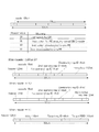
- FIG. 5A shows pseudo code corresponding to the loop portion of the process of mapping to the PE array in this embodiment.
- the pseudo code reads the data from the array A, adds the variable a, and writes it to the array B, for a total of 8 iterations for elements 0 to 7 of the array A. This is the program code to be executed in the configuration.
- FIG. 5B shows a case where the processing of FIG. 5A is mapped to PEs PE0, PE1, PE2, PE4 and PE10 in the PE array group of the SIMD processor of this embodiment. Indicates the instruction to be performed.
- add shown in FIG. 5B means an addition instruction, and has two source register number designations (A and cm) and one destination register number designation (1sx).
- a single alphabet (A, B, a) represents a constant (A is the absolute address of array A in this case).
- the instruction buffer (instb) 11 When executing the instruction stored in the instruction buffer (instb) 11, if a constant is specified as an operand, it is assumed that the constant is stored in the register of register number 0 (ie, r0), and the register r0 Operates to read a value.
- the destination register number is specified by a combination of a PE number and a register name. For example, if it is 1 sx, the operation is performed so that the operation result is stored in the sx register of the PE with PE number 1.
- CP30 in order for CP30 to store the instruction “add A, cm, 1sx” in the instruction buffer (instb) 11 of PE0, the “header” part is set to 10, and the “opcode” part is set.
- a bit string representing an add instruction “1st operating reg ID” is 0, “2nd operating reg ID” is 0xd, “Destination reg ID” is 0xe, and (the PE number of the operation result storage destination is 1) “PEID part ”,“ Counter ”part is 1 instruction,“ header ”part is 11,“ data ”part is absolute address of array A,“ Target reg ID ”part is 0, (add Since the PE number of the owner of the instruction storage instb is 0) "Target. EID "the prepared instructions and which is set to 0, it is sufficient to run the CP30.
- gld and gst shown in FIG. 5B are a load instruction and a store instruction for the global memory, respectively.
- the load instruction has the load target address as the first source operand without having the second source operand, and has the designation of the destination register number of the storage destination of the loaded data.
- the store instruction has a store target address as the first source operand, a register number storing the write data as the second source operand, and does not have a destination register number designation (indicated as NULL in FIG. 5B).
- 1sx, 2sx, 4sx, 4sy, and NULL in the destination field designation of each instruction are sx of PE1, sx of PE2, sx of PE4, Indicates sy and no destination.
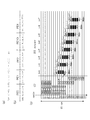
- FIG. 5 (c) shows, as an example, a time chart of the operation from when the instruction code of FIG. 5 (b) is distributed to the PE array by the CP 30 until the operation ends.
- the vertical axis represents time (unit: cycle)
- the horizontal axis represents the operation of the CP 30 and the operation on the PE side.
- the operation on the PE side is displayed separately for each iteration.
- the operation status of the CP 30 and PE in each cycle is shown.
- INSTB_BC (PE0) written at the top of the column indicating the operation of CP30 reads an instruction whose “header” portion is “10” (and an instruction whose subsequent “header” portion is “11”). Indicates that the operation of distributing to PE0 has occurred in the cycle.
- GO (1, cm) means that an instruction whose “header” part is “11” and whose value of the “data” part is “1” is read out of PE0, PE1, PE2, PE4, and PE10. This indicates that an operation in which the instruction in the instruction buffer (instb) 11 writes 1 as the value of the “data” part of the instruction to the register cm of the PE including the register cm as a source operand has occurred in the cycle.
- the CLD and CST perform load operation and store operation via the cache memory or the like to the global memory generated as a result of the arbitration by the global access arbitration unit 50 due to the issuing of the gld and gst instructions on the PE side, respectively.
- PEx represents a cycle in which a PE with a PE number x executes an instruction.
- PEx / y indicates that PEx and PEy executed an instruction in the same cycle.
- * or + is added to the end of PEx that executed the gld or gst instruction.
- a dotted arrow indicates a flow from when the gld instruction is executed on PE1 until load data is sent to PE2.
- a black rectangle in FIG. 5C represents a load data waiting cycle, and “-” represents a transfer cycle between PEs.
- the filled black circle indicates that the instruction is executed on the corresponding PE (horizontal axis).
- An arrow PEx ⁇ PEy indicates that data transfer has occurred between PEx and PEy.
- the load access delay for the global memory 40 is three cycles. Therefore, the arrow from PE1 to PE2 extends over 3 cycles.
- no crossing occurs between a plurality of arrows in the same direction. This indicates that there is no collision regarding data transfer using the coupling line between PEs over a total of 21 cycles in which the PE array performs systolic operation.
- the arrow in the left ⁇ right (or left ⁇ right) direction from PEx to PEy in cycle P indicates the connection between adjacent PEs in the direction of PEx ⁇ PEy (or PEx ⁇ PEy) in the cycle. Indicates that data transfer is performed using a line.
- the brightness of the arrows and filled circles is changed in order to make it easy to distinguish between individual iterations.
- FIGS. 5C and 6 show diagrams assuming that the delay of the load access by the PE for the global memory is 3 cycles.
- the delay is smaller than 3, for example, 2, the instruction assigned to PE10 may be assigned to PE9 as shown in FIG.
- the load access delay is larger than 3, for example, 4, for example, the instruction assigned to PE10 may be assigned to PE11 as shown in FIG. 7B.
- FIG. 8 shows pseudo code when the program code of FIG. 5A is sequentially executed on the CP 30.
- CADD represents an add instruction.
- CLD and CST represent a memory load instruction and a memory store instruction, respectively. These are all instructions whose “header” part is 00.
- the performance improvement is small when the number of iterations is small. However, if the number of iterations is 1000, the 5 cycles required to distribute the instructions to the PE array can be ignored. Further, in this embodiment, it can be executed with a throughput of one cycle for each iteration. On the other hand, referring to FIG. 7, when the same processing is executed on the CP 30, it takes 6 cycles for each iteration. Therefore, the SIMD processor of the present invention provides a performance improvement of about 6 times.
Landscapes
- Engineering & Computer Science (AREA)
- Theoretical Computer Science (AREA)
- Computer Hardware Design (AREA)
- Physics & Mathematics (AREA)
- General Engineering & Computer Science (AREA)
- General Physics & Mathematics (AREA)
- Software Systems (AREA)
- Computing Systems (AREA)
- Advance Control (AREA)
- Multi Processors (AREA)
Abstract
The disclosed SIMD processor enables a program to be processed at high speed using processing elements of the SIMD processor without modifying data arrangement upon global memory. The SIMD processor is provided with a control processor (CP) and a plurality of processing elements (PEs), wherein the plurality of PEs perform an SIMD operation for executing a single instruction issued from the CP, a specific PE among the plurality of PEs performs an instruction/data distribution operation for receiving the instruction and data issued from the CP, and for the instruction that has been broadcast to each PE from the CP in the instruction/data distribution operation, each of the PEs performs a systolic operation for execution after source operands of the instruction have been collected.
Description
(関連出願についての記載)
本発明は、日本国特許出願:特願2010-038976号(2010年2月24日出願)の優先権主張に基づくものであり、同出願の全記載内容は引用をもって本書に組み込み記載されているものとする。 (Description of related applications)
The present invention is based on the priority claim of Japanese patent application: Japanese Patent Application No. 2010-038976 (filed on Feb. 24, 2010), the entire description of which is incorporated herein by reference. Shall.
本発明は、SIMD(Single Instruction Multiple Data)プロセッサに関する。
The present invention relates to a SIMD (Single Instruction Multiple Data) processor.
図9は、非特許文献1に記載されたSIMDプロセッサの構成を示す図である。図9を参照すると、SIMDプロセッサは、複数の演算要素(PE:Processing Element)110と、複数のPE110に対して同一の命令を発行する制御プロセッサ(CP:Control Processor)130とを有する。SIMDプロセッサによると、安価なハードウェアに基づいて、高い演算性能を実現することができる。
FIG. 9 is a diagram showing the configuration of the SIMD processor described in Non-Patent Document 1. Referring to FIG. 9, the SIMD processor includes a plurality of computing elements (PE: Processing Element) 110 and a control processor (CP: Control Processor) 130 that issues the same instruction to the plurality of PEs 110. According to the SIMD processor, high computing performance can be realized based on inexpensive hardware.
SIMDプロセッサにおいては、CP130の制御下で、CP130が管理するグローバルメモリ(Global Memory)140上の所定位置に配置されたデータを、アドレス順に次々とPE110側のローカルメモリ(Local Memory)120に読み込んだ後、全PE110はCP130から発行される命令に従って一斉に各自のローカルメモリ120上のデータを対象とする演算を行う。
In the SIMD processor, under the control of the CP 130, the data arranged at a predetermined position on the global memory (Global Memory) 140 managed by the CP 130 is sequentially read into the local memory (Local Memory) 120 on the PE 110 side in the order of addresses. Thereafter, all the PEs 110 perform calculations on the data in their local memory 120 at the same time in accordance with instructions issued from the CP 130.
なお、特許文献1に、SIMD型とシストリックアレイ型の構成を切り替えることができる画像処理プロセッサが記載されている。
Note that Patent Document 1 describes an image processor that can switch between a SIMD type and a systolic array type configuration.
プログラムをSIMDプロセッサに移植して並列処理により高速化するには、一般に、グローバルメモリ140上のデータをPEアレイに読み込む際に都合が良いように、グローバルメモリ140上のデータ配置を変更する必要がある。しかし、グローバルメモリ140上のデータ配置を変更するには、アルゴリズムを設計し直さねばならない場合があり、プログラム開発者にとって大きな負担となっている。このことは、SIMDプロセッサの利用を妨げる要因となっている。
In order to increase the speed by parallel processing by porting a program to a SIMD processor, it is generally necessary to change the data arrangement on the global memory 140 so that it is convenient to read the data on the global memory 140 into the PE array. is there. However, in order to change the data arrangement on the global memory 140, it may be necessary to redesign the algorithm, which is a heavy burden on the program developer. This is a factor that hinders the use of the SIMD processor.
プログラム開発者によるグローバルメモリ140上のデータ配置の変更作業を容易にするために、図9に示したSIMDプロセッサのように各PE110にローカルにメモリブロックを持たせる代わりに、動的再構成型プロセッサのように多数のメモリブロックと多数のPEとの間を豊富な配線(例えばクロスバー)で接続する方法が考えられる。しかし、この方法によると、SIMDプロセッサに多数の配線回路を追加する必要があるため、SIMDプロセッサを実現するためのハードウェアが高価となる。
In order to facilitate the work of changing the data arrangement on the global memory 140 by the program developer, instead of having each PE 110 locally have a memory block like the SIMD processor shown in FIG. 9, a dynamically reconfigurable processor As described above, a method of connecting a large number of memory blocks and a large number of PEs with abundant wiring (for example, crossbars) can be considered. However, according to this method, since it is necessary to add a large number of wiring circuits to the SIMD processor, hardware for realizing the SIMD processor becomes expensive.
以上のことから、安価なハードウェア構成に基づくSIMDプロセッサにプログラムを移植するためには、グローバルメモリ140上のデータ配置を変更する必要があり、グローバルメモリ140上のデータ配置を変更するには、アルゴリズムの変更が必要となるため、プログラム開発者にとって大きな負担となり、SIMDプロセッサの利用が妨げられる。
From the above, in order to port a program to a SIMD processor based on an inexpensive hardware configuration, it is necessary to change the data arrangement on the global memory 140. To change the data arrangement on the global memory 140, Since the algorithm needs to be changed, it becomes a heavy burden on the program developer, and the use of the SIMD processor is prevented.
そこで、グローバルメモリ上のデータ配置を変更することなく、SIMDプロセッサの演算要素を活用してプログラムを高速に処理できるようにすることが課題となる。本発明の目的は、かかる課題を解決するSIMDプロセッサを提供することにある。
Therefore, there is a problem in that it is possible to process a program at high speed by utilizing the arithmetic element of the SIMD processor without changing the data arrangement on the global memory. An object of the present invention is to provide a SIMD processor that solves such problems.
本発明の第1の視点に係るSIMDプロセッサは、
制御プロセッサ(CP:Control Processor)と複数の演算要素(PE:Processing Element)とを備えたSIMD(Single Instruction Multiple Data)プロセッサであって、
前記複数のPEが前記CPから発行された単一の命令を実行するSIMD動作を行うとともに、
前記CPが前記複数のPEのそれぞれに対して相異なる命令又は相異なる命令及びデータを分配する命令・データ分配動作を行い、
前記複数のPEは、それぞれ、命令のソースオペランドが揃った後に前記命令・データ分配動作において前記CPから送付された命令を実行するシストリック動作を行う。 The SIMD processor according to the first aspect of the present invention is:
A SIMD (Single Instruction Multiple Data) processor comprising a control processor (CP: Control Processor) and a plurality of computing elements (PE: Processing Element),
The plurality of PEs perform a SIMD operation to execute a single instruction issued from the CP,
The CP performs a command / data distribution operation for distributing different commands or different commands and data to each of the plurality of PEs,
Each of the plurality of PEs performs a systolic operation of executing an instruction sent from the CP in the instruction / data distribution operation after the source operands of the instruction are prepared.
本発明に係るSIMDプロセッサによると、グローバルメモリ上のデータ配置を変更することなく、SIMDプロセッサの演算要素を活用してプログラムを高速に処理することができる。
According to the SIMD processor according to the present invention, it is possible to process a program at high speed by utilizing the arithmetic elements of the SIMD processor without changing the data arrangement on the global memory.
第1の展開形態によると、上記第1の視点に係るSIMDプロセッサが提供される。
According to the first development form, the SIMD processor according to the first viewpoint is provided.
第2の展開形態によると、前記CPは、前記命令・データ分配動作において各PEに命令を分配するために、全PEに対する命令発行パスを逐次的かつ排他的に利用する、SIMDプロセッサが提供される。
According to a second mode of deployment, the CP is provided with a SIMD processor that sequentially and exclusively uses instruction issue paths for all PEs in order to distribute instructions to each PE in the instruction / data distribution operation. The
第3の展開形態によると、、前記シストリック動作において、前記複数のPEは、それぞれ実行した演算命令の演算結果を他のPEに転送するとともに、他のPEから転送された演算結果を、前記命令・データ分配動作において送付された命令に対するソースオペランドとする、SIMDプロセッサが提供される。
According to a third development mode, in the systolic operation, the plurality of PEs transfer the operation results of the executed operation instructions to other PEs, and the operation results transferred from the other PEs are A SIMD processor is provided that serves as a source operand for instructions sent in an instruction / data distribution operation.
第4の展開形態によると、前記シストリック動作において、前記複数のPEは、それぞれ、前記CPから送付されたデータを、前記命令・データ分配動作において送付された命令に対するソースオペランドとする、SIMDプロセッサが提供される。
According to a fourth development mode, in the systolic operation, each of the plurality of PEs uses the data sent from the CP as a source operand for the instruction sent in the command / data distribution operation. Is provided.
第5の展開形態によると、前記シストリック動作において、前記複数のPEのそれぞれによるグローバルメモリアクセスを調停し、グローバルメモリに対するアクセスの排他性を保証する大域アクセス調停部(Global Access Arbiter)をさらに備えている、SIMDプロセッサが提供される。
According to a fifth embodiment, in the systolic operation, a global access arbitration unit (Global Access Arbiter) that arbitrates global memory access by each of the plurality of PEs and guarantees access exclusiveness to the global memory is further provided. A SIMD processor is provided.
第6の展開形態によると、前記複数のPEは、それぞれ、前記命令・データ分配動作中に動作を停止状態に保つためのフラグを格納するレジスタを備えている、SIMDプロセッサが提供される。
According to a sixth development mode, a SIMD processor is provided in which each of the plurality of PEs includes a register for storing a flag for keeping the operation stopped during the instruction / data distribution operation.
第7の展開形態によると、前記複数のPEは、それぞれ、前記SIMD動作と前記シストリック動作との間で動作を切り替えるためのフラグを格納するレジスタを備えている、SIMDプロセッサが提供される。
According to a seventh development mode, a SIMD processor is provided in which each of the plurality of PEs includes a register that stores a flag for switching the operation between the SIMD operation and the systolic operation.
第8の展開形態によると、前記複数のPEは、それぞれ、前記CPから発行された命令を自身の命令バッファに格納するか否かを選択するセレクタを備えている、SIMDプロセッサが提供される。
According to an eighth development mode, a SIMD processor is provided in which each of the plurality of PEs includes a selector that selects whether or not to store an instruction issued from the CP in its own instruction buffer.
本発明によるSIMDプロセッサは、PEアレイ全体が制御プロセッサ(CP)から発行される単一の命令を実行するSIMD動作を行うとともに、CPが命令発行パスを利用して、相異なる命令コードやデータを逐次的に各PEに送信する命令・データ分配動作を行い、PEアレイ内の各PEは、CPからサイクル毎に放送されてくる命令ではなく、命令・データ分配動作によりCPから送信された命令を、当該命令のソースオペランドが揃った時点で実行し、当該命令の実行結果を指定された他のPEのレジスタ資源に書き込むように指定するシストリック動作を行う。また、シストリック動作中に、各PEは、命令のオペランドが他のPE又はCPからの送付データによって書き込まれることで揃った後に、命令の実行を開始し、演算命令の場合には演算結果を他のPEに送付し、メモリアクセス命令の場合にはグローバルメモリにアクセスする。
The SIMD processor according to the present invention performs SIMD operation in which the entire PE array executes a single instruction issued from the control processor (CP), and the CP uses the instruction issue path to transmit different instruction codes and data. The instruction / data distribution operation to be sequentially transmitted to each PE is performed, and each PE in the PE array receives the instruction transmitted from the CP by the instruction / data distribution operation, not the instruction broadcast from the CP every cycle. When the source operands of the instruction are ready, a systolic operation is performed to specify that the execution result of the instruction is written to the register resource of another designated PE. In addition, during the systolic operation, each PE starts executing the instruction after the operands of the instruction are written by data sent from other PEs or CPs. It is sent to another PE, and in the case of a memory access command, the global memory is accessed.
次に、本発明に係るSIMDプロセッサによってもたらされる効果について説明する。
Next, effects brought about by the SIMD processor according to the present invention will be described.
従来のSIMDプロセッサにおいては、全PEが同一の命令を実行するため、メモリアクセス命令が全PEで一斉に発生してしまう。したがって、かかるSIMDプロセッサの性能を引き出すには、各PEがアクセス可能なメモリ空間を、各PEにローカルな空間に限定する必要があった。
In the conventional SIMD processor, since all PEs execute the same instruction, memory access instructions are generated simultaneously in all PEs. Therefore, in order to extract the performance of the SIMD processor, it is necessary to limit the memory space accessible to each PE to a space local to each PE.
しかし、本発明のSIMDプロセッサによると、命令・データ分配動作により、各PEに互いに異なる命令を発行することができる。したがって、PE間でメモリアクセス命令を実行するタイミングをずらしたり、特定のPEにのみメモリアクセス命令を行わせたりすることができる。このとき、メモリ上でのデータ配置を元のままとし、PEがアクセス可能なメモリ空間をグローバルなメモリ空間に広げたとしても、単一のハードウェア資源であるグローバルなメモリ空間の利用に際して多数のPEが競合する頻度を低下させることができ、プロセッサの演算資源による処理性能を向上させることができる。
However, according to the SIMD processor of the present invention, different instructions can be issued to each PE by the instruction / data distribution operation. Accordingly, it is possible to shift the timing of executing the memory access instruction between the PEs, or to allow only a specific PE to execute the memory access instruction. At this time, even if the data arrangement on the memory is left as it is and the memory space accessible by the PE is expanded to the global memory space, there are a number of cases when using the global memory space that is a single hardware resource. The frequency of competing PEs can be reduced, and the processing performance of the processing resources of the processor can be improved.
ゆえに、本発明に係るSIMDプロセッサによると、プログラムのメモリ上におけるデータ配置を変更することなく、SIMDプロセッサが有する演算資源を利用した処理の高速化が可能となる(第1の効果)。
Therefore, according to the SIMD processor according to the present invention, it is possible to speed up the processing using the operation resource of the SIMD processor without changing the data arrangement on the memory of the program (first effect).
また、CPがPEアレイに対して命令・データ分配動作を行うことで、1イタレーション分の処理をデータフローグラフとして表現したときの各演算ノードに相当する個々の演算命令及び関連する定数データを各PEに分配し、データフローグラフにおける各演算ノードを各PEに割当てることができる。さらに、CPがPEアレイにシストリック動作モードで実行を開始させるために、起動データを1つ以上のPEに対して繰り返し発行することで、異なるイタレーションを次々と重畳した形で起動し、PEアレイに処理させることができる。
In addition, the CP performs an instruction / data distribution operation on the PE array, so that each arithmetic instruction corresponding to each arithmetic node and related constant data when processing for one iteration is expressed as a data flow graph It is possible to distribute to each PE and assign each operation node in the data flow graph to each PE. Further, in order for the CP to start execution in the systolic operation mode in the PE array, the activation data is repeatedly issued to one or more PEs, thereby starting up the different iterations one after another. The array can be processed.
したがって、本発明に係るSIMDプロセッサによると、プログラムのループ部分のうちのイタレーション間でデータ依存関係がない部分(並列ループ部分)に対する処理を、グローバルメモリ上のデータ配置を変更することなく、PEアレイを利用してパイプライン的に処理することで、高速化することができる(第2の効果)。
Therefore, according to the SIMD processor according to the present invention, the processing for the portion (parallel loop portion) having no data dependency among the iterations in the loop portion of the program can be performed without changing the data arrangement on the global memory. By performing processing in a pipeline manner using an array, the speed can be increased (second effect).
上記の命令・データ分配動作を実現するには、従来のSIMDプロセッサに設けられた全PEへの命令発行パスの回路資源、並びに、各PEからCP及びCPから各PEへのデータ配線回路資源をそのまま利用することができる。また、PE毎からグローバルメモリ空間へのアクセスを行うための結線として、従来のSIMDプロセッサに設けられたCPとPEアレイ間でスカラーデータをやり取りするための配線回路資源をそのまま利用することができる。さらに、データフローグラフ上の演算ノード同士が互いにデータを送受信する動作を行うPE間において、データを送受信するためのPE間結線として、従来のSIMDプロセッサに設けられた隣接PE間の配線資源をそのまま利用することができる。
In order to realize the above instruction / data distribution operation, the circuit resources of the instruction issue path to all PEs provided in the conventional SIMD processor and the data wiring circuit resources from each PE to the CP and from the CP to each PE are allocated. It can be used as it is. Further, as a connection for accessing the global memory space from each PE, a wiring circuit resource for exchanging scalar data between a CP and a PE array provided in a conventional SIMD processor can be used as it is. Furthermore, between PEs that perform operations in which operation nodes on the data flow graph transmit / receive data to / from each other, as a connection between PEs for transmitting / receiving data, the wiring resources between adjacent PEs provided in the conventional SIMD processor are used as they are. Can be used.
したがって、本発明に係るSIMDプロセッサによると、従来のSIMDプロセッサに少量の回路を追加するだけで、上記第1の効果及び第2の効果が得られる(第3の効果)。
Therefore, according to the SIMD processor of the present invention, the first effect and the second effect can be obtained (third effect) only by adding a small amount of circuit to the conventional SIMD processor.
(実施形態)
次に、実施形態に係るSIMDプロセッサについて、図面を参照して説明する。 (Embodiment)
Next, the SIMD processor according to the embodiment will be described with reference to the drawings.
次に、実施形態に係るSIMDプロセッサについて、図面を参照して説明する。 (Embodiment)
Next, the SIMD processor according to the embodiment will be described with reference to the drawings.
本実施形態のSIMDプロセッサについて説明する前に、比較のために、従来のSIMDプロセッサの構成を示す。図10は、従来のSIMDプロセッサに含まれるPEアレイ中の1つのPE110の構成を示す図である。
Before describing the SIMD processor of this embodiment, the configuration of a conventional SIMD processor is shown for comparison. FIG. 10 is a diagram showing a configuration of one PE 110 in a PE array included in a conventional SIMD processor.
図10を参照すると、PE110は、CP130(図9)から発行された命令を格納するための命令バッファ(instb)111、汎用レジスタ(General Purpose Register)r0~r7、演算器(ALU:Arithmetic Logic Unit)112、PE間結合網への出入り口(Left/Right Inter PE Connection)、PE毎のローカルメモリ(Local Memory)120を有する。すべてのPE110は、サイクル毎にCP130から発行された単一の命令を一斉に実行する。
Referring to FIG. 10, the PE 110 stores an instruction buffer (instb) 111 for storing instructions issued from the CP 130 (FIG. 9), general purpose registers (General Purpose Registers) r0 to r7, and arithmetic units (ALU: Arithmetic Logic Unit). ) 112, and an entry / exit to the connection network between PEs (Left / Right Inter PE Connection), and a local memory 120 for each PE (Local Memory). All the PEs 110 simultaneously execute a single instruction issued from the CP 130 every cycle.
図1は、本実施形態に係るSIMDプロセッサに含まれるPEアレイ中の1PE10の構成を示す。図1を参照すると、PE10は、命令バッファ(instb)11、汎用レジスタ(General Purpose Register)r0~r15、演算器(ALU:Arithmetic Logic Unit)12、PE間結合網への出入り口(Left/Right Inter PE Connection)、PE毎のローカルメモリ(Local Memory)20を有する。PE10は、さらに、レジスタstop,mode、及び、セレクタselを有する。図1において、図10に対して追加された構成要素(太線部分)、すなわち、レジスタstop,mode,セレクタsel,レジスタcm,sx,syのそれぞれについて説明する。
FIG. 1 shows a configuration of 1 PE 10 in a PE array included in a SIMD processor according to this embodiment. Referring to FIG. 1, the PE 10 includes an instruction buffer (instb) 11, general purpose registers (General Purpose Registers) r 0 to r 15, an arithmetic unit (ALU: Arithmetic Logic Unit) 12, and an entrance / exit to a connection network between PEs (Left / Right Interchange). PE Connection) and local memory 20 for each PE. The PE 10 further includes registers stop and mode and a selector sel. In FIG. 1, components (thick line portions) added to FIG. 10, that is, registers stop, mode, selector sel, registers cm, sx, and sy will be described.
レジスタstopは、命令・データ分配動作中にPE10の動作を停止状態に保つための制御レジスタである。
The register stop is a control register for keeping the operation of the PE 10 stopped during the instruction / data distribution operation.
レジスタmodeは、シストリック動作と従来のSIMD動作とを切り替えるための1ビットの動作モード選択レジスタである。
The register mode is a 1-bit operation mode selection register for switching between a systolic operation and a conventional SIMD operation.
セレクタselは、CPから発行された命令を命令バッファ(instb)11に格納するか否かを選択するセレクタである。レジスタcm,sx,syは、シストリック動作中に、当該レジスタへのライトが発生する度に、所定カウンターレジスタがデクリメントされるデータ待合せ機能を有する汎用レジスタ(待合せレジスタ)群である。
The selector sel is a selector that selects whether or not an instruction issued from the CP is stored in the instruction buffer (instb) 11. The registers cm, sx, and sy are a general-purpose register (waiting register) group having a data waiting function in which a predetermined counter register is decremented each time a write to the register occurs during a systolic operation.
図2は、本実施形態に係るSIMDプロセッサに含まれる制御プロセッサ(CP)30の構成を概略的に示す図である。図2を参照すると、CP30は、従来のSIMDプロセッサにおけるCP130と同様に、自ら演算を行うためのデータパスを有し、命令・データキャッシュ(Instruction/Data Cache)31、及びメモリアクセス調整部であるアービタ(Arbiter)33を介してグローバルメモリ(Global Memory)40に接続されている。CP30は、自らのデータパスで実行すべき命令及びPEアレイ全体に放送すべき命令を、グローバルメモリ40から読み出して発行し、CP30上の演算用データ及びPE10のローカルメモリ20との間で送受信されるデータを、グローバルメモリ40から読み出したり、グローバルメモリ40に書き込んだりする。
FIG. 2 is a diagram schematically showing the configuration of the control processor (CP) 30 included in the SIMD processor according to the present embodiment. Referring to FIG. 2, CP 30 has a data path for performing its own operation, and is an instruction / data cache (Instruction / Data Cache) 31, and a memory access adjustment unit, like CP 130 in the conventional SIMD processor. It is connected to a global memory 40 via an arbiter 33. The CP 30 reads and issues commands to be executed in its own data path and commands to be broadcast to the entire PE array from the global memory 40, and is transmitted and received between the calculation data on the CP 30 and the local memory 20 of the PE 10. Data to be read from the global memory 40 or written to the global memory 40.
図3は、本実施形態に係るSIMDプロセッサにおける命令フォーマットを一例として示す図である。本実施形態のSIMDプロセッサにおけるCP30は、従来のSIMDプロセッサにおけるCP130とは異なり、命令若しくはデータ又はこれらの両方を特定のPEに同時に送付し、特定の1つのPE又は指定された複数のPEに実行の開始を指定することができるように、図3に示すような命令フォーマットから成る命令セットを用いる。
FIG. 3 is a diagram illustrating an example of an instruction format in the SIMD processor according to the present embodiment. The CP 30 in the SIMD processor of the present embodiment is different from the CP 130 in the conventional SIMD processor, and sends instructions and / or data to a specific PE at the same time and executes them to a specific PE or a plurality of designated PEs. An instruction set having an instruction format as shown in FIG. 3 is used.
図3を参照すると、CP30の命令フォーマットは、命令のヘッダ(header)部のビットパタンに応じて、異なるフォーマットを有する。
Referring to FIG. 3, the instruction format of CP30 has a different format according to the bit pattern of the header section of the instruction.
「header」部のビットパタンが“00”である場合には、CP30上で動作する命令であることを示す。
When the bit pattern of the “header” part is “00”, it indicates that the instruction operates on the CP 30.
「header」部のビットパタンが“01”である場合には、SIMDモードで動作する場合におけるPEアレイの動作を指定するPE命令であることを示す。
When the bit pattern of the “header” portion is “01”, this indicates a PE instruction that specifies the operation of the PE array when operating in the SIMD mode.
「header」部のビットパタンが“10”である場合には、命令Aは特定PE10に分配すべきものであることを示し、後続の命令として、必ずヘッダ部のビットパタンが“11”の命令Bが続き、命令Bの「Target PEID」部が示すPE番号のPEの命令バッファ(instb)11に命令Aを書き込み、かつ、命令Bの「Target reg ID」部が示すPE番号のPEのレジスタに命令Bの「data」部を書き込む動作を指定する。
When the bit pattern of the “header” part is “10”, it indicates that the instruction A is to be distributed to the specific PE 10, and as a subsequent instruction, an instruction B whose bit pattern of the header part is always “11” The instruction A is written to the instruction buffer (instb) 11 of the PE of the PE number indicated by the “Target PEID” part of the instruction B, and the PE register of the PE number indicated by the “Target reg ID” part of the instruction B is written. Specifies the operation of writing the “data” part of the instruction B.
「header」部のビットパタンが“11”である場合には、その命令の「Target PEID」部が示すPE番号のPEの「Target reg ID」部が示す番号のレジスタに「data」部の値を書き込む動作、又は、「Target reg ID」部がcmの場合は、命令バッファ(instb)11内に格納中の命令がソースオペランドとしてcmを持つPE10のレジスタcmにdata部の値を書き込む動作を指定する。
When the bit pattern of the “header” part is “11”, the value of the “data” part is stored in the register of the number indicated by the “Target reg ID” part of the PE of the PE number indicated by the “Target PEID” part of the instruction. Or when the “Target reg ID” part is cm, the instruction stored in the instruction buffer (instb) 11 writes the value of the data part to the register cm of the PE 10 having cm as the source operand. specify.
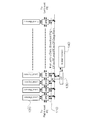
図4は、本実施形態に係るSIMDプロセッサにおけるPEアレイの全体構成を示す。図4を参照すると、太線の部分は、従来のSIMDプロセッサに対して、個々のPE10以外に、本発明で新たに付け加えた回路要素である大域アクセス調停部(Global Access Arbiter)50を示す。
FIG. 4 shows the overall configuration of the PE array in the SIMD processor according to this embodiment. Referring to FIG. 4, the bold line portion indicates a global access arbitration unit (Global Access Arbiter) 50, which is a circuit element newly added in the present invention, in addition to the individual PEs 10, with respect to the conventional SIMD processor.
大域アクセス調停部50は、全PE20のローカルメモリブロックを、まとめて多バンクのキャッシュメモリ本体として利用できるように管理するモジュールであり、シストリック動作モード中に、多数のPE10から同時にメモリアクセスが発生した場合のメモリアクセスを調停する。
The global access arbitration unit 50 is a module that manages the local memory blocks of all the PEs 20 so that they can be used together as a multi-bank cache memory body, and memory access is simultaneously generated from a large number of PEs 10 during the systolic operation mode. If this occurs, the memory access is arbitrated.
なお、大域アクセス調停部50の実装方式として、次の方式が考えられる。すなわち、2以上のPEから同時にメモリアクセス要求があると、PEアレイ全体の動作を一時停止させ、各PEのメモリアクセス要求に一つずつ順に応えてから、PEアレイの動作を再開させるという、最も性能が低いもののハードウェア実現コストが安い実装方式が考えられる。一方、全てのPEのローカルメモリブロックをクロスバー機構で接続し、できるだけ短い遅延で多数のメモリアクセス要求に応えるという、最も性能が高いもののハードウェア実現コストが高い実装方式が考えられる。任意のプログラムコードを重畳実行させた場合における最大メモリアクセス遅延を静的に定めることができれば、いずれの実装方式を採用してもよい。
In addition, as a mounting method of the global access arbitration unit 50, the following method can be considered. In other words, when there are memory access requests from two or more PEs simultaneously, the operation of the entire PE array is temporarily stopped, the memory access requests of each PE are answered one by one, and then the operation of the PE array is resumed. An implementation method with low performance but low hardware implementation cost is conceivable. On the other hand, a mounting method that has the highest performance but high hardware implementation cost is conceivable, in which local memory blocks of all PEs are connected by a crossbar mechanism to respond to a large number of memory access requests with the shortest possible delay. Any mounting method may be adopted as long as the maximum memory access delay can be determined statically when arbitrary program code is executed in a superimposed manner.
次に、実施形態のSIMDプロセッサ全体の動作について説明する。まず、CP30は、サイクル毎、プログラムカウンタ(PC:Program Counter)35の値が指すアドレスの命令とその次のアドレスの命令の2つの命令を同時に読み出す。ただし、PC35のカウント値がサイクル毎に+1されるのか又は+2されるのか、及び、読み出された命令をどのような形で処理するのかについては、読み出された先頭命令Aの「header」部の値に応じて以下のように決定する。
Next, the operation of the entire SIMD processor of the embodiment will be described. First, for each cycle, the CP 30 simultaneously reads two instructions, the instruction at the address indicated by the value of the program counter (PC: Program Counter) 35 and the instruction at the next address. However, whether the count value of the PC 35 is incremented or decremented every cycle and how the read instruction is processed is determined by “header” of the read first instruction A. It is determined as follows according to the value of the part.
読み出された先頭命令Aの「header」部の値が“00”である場合には、CP命令であることを表し、次サイクルまでにPC35のカウント値は+1され、命令AはCP30の処理部で実行される。
When the value of the “header” portion of the read first instruction A is “00”, this indicates that it is a CP instruction, and the count value of the PC 35 is incremented by 1 until the next cycle, and the instruction A is processed by the CP30. Executed in the department.
読み出された先頭命令Aの「header」部の値が“01”である場合には、PE命令であることを表し、PC35のカウント値は+1され、次サイクルまでに命令AがPEアレイに送られ、次々サイクルに全PE10は命令Aを実行する。
When the value of the “header” portion of the read first instruction A is “01”, this indicates that it is a PE instruction, the count value of the PC 35 is incremented by 1, and the instruction A is stored in the PE array by the next cycle. All PEs 10 execute instruction A in the next cycle.
読み出された先頭命令Aの「header」部の値が“10”である場合には、命令・データ分配動作の指定であることを表し、PC35のカウント値は+2され、次サイクルまでに、全PE10のレジスタstopをONにセットし、後続命令Bの「target PEID」部が指定するPE番号のPEの命令バッファ(instb)11に、命令Aの「header」部に命令Aの「counter」部の2ビットをコピーした上で命令Aを書き込む。同様に、次サイクルまでに、同PEに含まれる、命令Bの「Target reg ID」部が指定するレジスタに、命令Bの「data」部の値を書き込む。
When the value of the “header” portion of the read first instruction A is “10”, it indicates that the instruction / data distribution operation is designated, and the count value of the PC 35 is incremented by 2, and by the next cycle, The register stop of all PEs 10 is set to ON, the instruction buffer (instb) 11 of the PE of the PE number designated by the “target PEID” part of the subsequent instruction B, and the “counter” of the instruction A in the “header” part of the instruction A The instruction A is written after the 2 bits of the copy are copied. Similarly, by the next cycle, the value of the “data” part of the instruction B is written to the register specified by the “Target reg ID” part of the instruction B included in the PE.
最後に、読み出された先頭命令Aの「header」部の値が“01”である場合には、シストリック動作の指定であることを表し、PC35のカウント値は+1され、次サイクルまでに、全PEのレジスタstop及びレジスタmodeをそれぞれOFF及びONにセットし、命令Aの「target PEID」部が指定するPE番号のPEに含まれる、命令Aの「Target reg ID」部が指定するレジスタに、命令Aの「data」部の値を書き込む。
Finally, when the value of the “header” portion of the read first instruction A is “01”, this indicates that the systolic operation is designated, and the count value of the PC 35 is incremented by one, and until the next cycle The register stop and register mode of all PEs are set to OFF and ON, respectively, and the register specified by the “Target reg ID” part of the instruction A included in the PE of the PE number specified by the “target PEID” part of the instruction A The value of the “data” part of the instruction A is written in
図3を参照すると、「header」部の値が“10”の命令は、「counter」部を含む。「counter」部には、当該命令が持つソースオペランドのうち、「待合せレジスタ」の数に等しいか又はそれよりも大きい値が設定されているものとする。
Referring to FIG. 3, an instruction having a “header” value of “10” includes a “counter” portion. It is assumed that a value equal to or greater than the number of “waiting registers” among the source operands of the instruction is set in the “counter” portion.
PE側では、レジスタmodeがONの期間中において、命令バッファ(instb)11に格納されている命令Cのソースオペランドに指定されたいずれかの「待合せレジスタ」に対し、書き込み動作が起きるたびに、命令Cの「counter」部が1だけデクリメントされる。そして、「counter」部がゼロにデクリメントされたサイクルに命令Cの実行を開始する。命令Cの実行は1サイクルで終了し、その実行結果を、命令Cの「PEID」部が指定するPE番号のPEに含まれる、命令Cの「Destination reg ID」部が指定するレジスタに書き込むために、実行結果値は次サイクルまでにPE結合線上に送り出される。また、命令Cの実行終了と同時に、命令Cの「counter」部には、命令Cの「header」部の値がコピーされる。
On the PE side, every time a write operation occurs to any “waiting register” designated as the source operand of the instruction C stored in the instruction buffer (instb) 11 while the register mode is ON, The “counter” part of instruction C is decremented by one. Then, the execution of the instruction C is started in the cycle in which the “counter” part is decremented to zero. Execution of instruction C is completed in one cycle, and the execution result is written to the register specified by the “Destination reg ID” part of instruction C included in the PE of the PE number specified by the “PEID” part of instruction C. In addition, the execution result value is sent out on the PE coupling line by the next cycle. Simultaneously with the end of execution of the instruction C, the value of the “header” part of the instruction C is copied to the “counter” part of the instruction C.
したがって、例えば、CP30がシストリック動作において、「Target reg ID」部に待合せレジスタsxが指定されている命令Aを実行した場合、命令Aの「target PEID」部が指定するPE番号のPE上のレジスタsxに対して書き込み動作Pが行われる。ここで、当該PEの命令バッファ(instb)11内の命令Cの「counter」部に値1が設定されており、かつ、レジスタsxが命令Cのソースオペランドのうちの唯一の「待合せレジスタ」である場合、上記のレジスタsxに対する書き込み動作Pの結果、当該PEは命令Cの実行を開始し、命令Cの実行終了と同時に、命令Cの「counter」部に、命令Cの「header」部の値である1を再度設定する。ただし、命令Cの実行終了と同じサイクルに、当該PEの待合せレジスタsxに対して書き込み動作が再度起きた場合には、「counter」部には、1ではなく、そのデクリメントした結果である0がセットされるため、命令Cは当該PE上で連続して実行される。
Therefore, for example, when CP30 executes an instruction A in which the waiting register sx is specified in the “Target reg ID” portion in the systolic operation, the PE number specified by the “target PEID” portion of the instruction A is on the PE. A write operation P is performed on the register sx. Here, the value “1” is set in the “counter” portion of the instruction C in the instruction buffer (instb) 11 of the PE, and the register sx is the only “waiting register” in the source operand of the instruction C. If there is, as a result of the write operation P to the register sx, the PE starts execution of the instruction C, and at the same time as the execution of the instruction C ends, the “counter” part of the instruction C includes The value 1 is set again. However, when the write operation to the queuing register sx of the PE occurs again in the same cycle as the end of the execution of the instruction C, the “counter” portion is not 1 but 0 which is the decrement result. Since it is set, the instruction C is continuously executed on the PE.
他の例として、CP30がシストリック動作において「Target reg ID」部に待合せレジスタcmが指定されている命令Aを実行した場合には、命令バッファ(instb)11内にcmをソースオペランドに持つすべてのPEに対し、cmへの書き込み動作Pが生じる。ここで、PEの命令バッファ(instb)11内の命令Cの「counter」部に値2が設定されており、cm及びsyがいずれも命令Cのソースオペランドである場合には、上記のCPによる命令Aの実行に起因するcmへの書き込み動作Pだけでは、当該PEが命令Cの実行を開始しないが、書き込み動作Pが発生したのと同一のサイクル、あるいはそれ以降のサイクルにおいて別途syへの書き込み動作Qが発生すれば、当該PEが命令Cの実行を開始する。そして、命令Cの実行終了と同時に、命令Cの「counter」部には、値2が命令Cの「header」部からコピーされて再度設定されるが、命令Cの実行終了と同一のサイクルに、当該PEの待合せレジスタsxとcmに対し、同時に書き込み動作が起きた場合には、「counter」部には、2ではなく、これを2回だけデクリメントした結果である0が再度セットされる。したがって、命令Cが当該PE上で連続して実行される。
As another example, when CP30 executes an instruction A in which the waiting register cm is specified in the “Target reg ID” part in the systolic operation, all having cm as a source operand in the instruction buffer (instb) 11 The writing operation P to cm occurs with respect to the PE. Here, when the value “2” is set in the “counter” part of the instruction C in the instruction buffer (instb) 11 of the PE, and cm and sy are both source operands of the instruction C, the above CP is used. The PE does not start executing the instruction C only by the write operation P to cm caused by the execution of the instruction A. However, the PE does not start the execution of the instruction C. When the write operation Q occurs, the PE starts executing the instruction C. At the same time as the end of execution of the instruction C, the value 2 is copied from the “header” part of the instruction C and set again in the “counter” part of the instruction C. When a write operation occurs simultaneously with respect to the queuing registers sx and cm of the PE, 0, which is the result of decrementing this twice only, is set in the “counter” section again. Therefore, the instruction C is continuously executed on the PE.
上記の2つの動作例からわかるように、CP30は「シストリック動作」指示命令の発行を通じて、命令バッファ(instb)11に格納されている命令の実行をPEに指示することができる。また、命令バッファ(instb)11に格納されている命令が、その実行結果の書き込み先として、他のPEの「待合せレジスタ」を指定している場合には、命令の実行がPE間を伝播する。また、CP30は、多数のPEのレジスタcmに対し書き込み動作を行うことが可能なので、同時に多数のPEを「待ち」状態から「実行」状態に移すこともできる。このように、CP30は「シストリック動作」指示命令の発行により、PEアレイ上にシストリック的な命令実行の連鎖を引き起こすことができる。
As can be seen from the above two operation examples, the CP 30 can instruct the PE to execute the instruction stored in the instruction buffer (instb) 11 by issuing the “systolic operation” instruction instruction. If the instruction stored in the instruction buffer (instb) 11 designates the “waiting register” of another PE as the write destination of the execution result, the execution of the instruction propagates between the PEs. . Further, since the CP 30 can perform a write operation on the registers cm of a large number of PEs, it is possible to simultaneously shift a large number of PEs from the “waiting” state to the “execution” state. In this manner, the CP 30 can cause a systolic instruction execution chain on the PE array by issuing a “systolic operation” instruction.
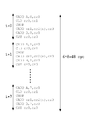
次に、具体的な実施例を用いて、実施形態に係るSIMDプロセッサの動作について説明する。図5(a)は、本実施例において、PEアレイにマップする処理のループ部分に相当する擬似コードである。図5(a)を参照すると、擬似コードは、配列Aからデータを読み出して変数aを加算して配列Bに書き込む動作を、配列Aの要素0から7までを対象に、計8回のイタレーションで行うプログラムコードである。
Next, the operation of the SIMD processor according to the embodiment will be described using a specific example. FIG. 5A shows pseudo code corresponding to the loop portion of the process of mapping to the PE array in this embodiment. Referring to FIG. 5 (a), the pseudo code reads the data from the array A, adds the variable a, and writes it to the array B, for a total of 8 iterations for elements 0 to 7 of the array A. This is the program code to be executed in the configuration.
図5(b)は、本実施形態のSIMDプロセッサのPEアレイ群のうちのPE0,PE1,PE2,PE4,PE10に対して、図5(a)の処理をマッピングした場合において、各PEに分配すべき命令を示す。
FIG. 5B shows a case where the processing of FIG. 5A is mapped to PEs PE0, PE1, PE2, PE4 and PE10 in the PE array group of the SIMD processor of this embodiment. Indicates the instruction to be performed.
ここで、図5(b)に示すaddは加算命令を意味し、2つのソースレジスタ番号指定(Aとcm)と1つのデスティネーションレジスタ番号指定(1sx)を持つ。単一アルファベット(A、B、a)は定数(Aはこの場合は、配列Aの絶対アドレス)を表す。命令バッファ(instb)11に格納されている命令の実行に際し、定数がオペランドに指定されている場合には、レジスタ番号0のレジスタ(すなわちr0)に定数が格納されていると見なし、レジスタr0から値を読出すように動作する。デスティネーションレジスタ番号指定は、PE番号とレジスタ名の組合せで指定する。例えば、1sxとなっていれば、PE番号が1のPEのsxレジスタに、演算結果を格納するように動作する。
Here, add shown in FIG. 5B means an addition instruction, and has two source register number designations (A and cm) and one destination register number designation (1sx). A single alphabet (A, B, a) represents a constant (A is the absolute address of array A in this case). When executing the instruction stored in the instruction buffer (instb) 11, if a constant is specified as an operand, it is assumed that the constant is stored in the register of register number 0 (ie, r0), and the register r0 Operates to read a value. The destination register number is specified by a combination of a PE number and a register name. For example, if it is 1 sx, the operation is performed so that the operation result is stored in the sx register of the PE with PE number 1.
なお、図1及び図3を参照すると、CP30に「add A,cm,1sx」という命令をPE0の命令バッファ(instb)11に格納させるには、「header」部を10、「opcode」部をadd命令を現すビット列、「1st operand reg ID」を0、「2nd operand reg ID」を0xd、「Destination reg ID」を0xe、(演算結果の格納先PE番号が1であることから)「PEID部」を1、「counter」部を1である命令と、当該命令に後続する、「header」部を11、「data」部を配列Aの絶対アドレス、「Target reg ID」部を0、(add命令の格納instbの持ち主のPE番号が0であることから)「Target PEID」を0とした命令とを用意し、CP30に実行させればよい。
Referring to FIGS. 1 and 3, in order for CP30 to store the instruction “add A, cm, 1sx” in the instruction buffer (instb) 11 of PE0, the “header” part is set to 10, and the “opcode” part is set. A bit string representing an add instruction, “1st operating reg ID” is 0, “2nd operating reg ID” is 0xd, “Destination reg ID” is 0xe, and (the PE number of the operation result storage destination is 1) “PEID part ”,“ Counter ”part is 1 instruction,“ header ”part is 11,“ data ”part is absolute address of array A,“ Target reg ID ”part is 0, (add Since the PE number of the owner of the instruction storage instb is 0) "Target. EID "the prepared instructions and which is set to 0, it is sufficient to run the CP30.
また、図5(b)に示したgld及びgstは、それぞれ、グローバルメモリに対するロード命令及びストア命令である。ロード命令は、第2ソースオペランドを持たずにロード対象アドレスを第1ソースオペランドとして持ち、ロードしたデータの格納先のデスティネーションレジスタ番号指定を持つ。ストア命令は、第1ソースオペランドとしてストア対象アドレス、第2ソースオペランドとしてライトデータを格納したレジスタ番号を有し、デスティネーションレジスタ番号指定を持たない(図5(b)ではNULLとした)。以上より、図5(b)において、各命令のデスティネーションフィールド指定における1sx,2sx,4sx,4sy及びNULLは、それぞれ、命令の実行結果の宛先がPE1のsx、PE2のsx、PE4のsx、sy及び宛先なしを示す。
In addition, gld and gst shown in FIG. 5B are a load instruction and a store instruction for the global memory, respectively. The load instruction has the load target address as the first source operand without having the second source operand, and has the designation of the destination register number of the storage destination of the loaded data. The store instruction has a store target address as the first source operand, a register number storing the write data as the second source operand, and does not have a destination register number designation (indicated as NULL in FIG. 5B). As described above, in FIG. 5B, 1sx, 2sx, 4sx, 4sy, and NULL in the destination field designation of each instruction are sx of PE1, sx of PE2, sx of PE4, Indicates sy and no destination.
図5(c)は、図5(b)の命令コードをCP30がPEアレイに分配し、動作を開始させてから終了するまでの動作のタイムチャートを一例として示す。図5(c)を参照すると、縦軸は時間(単位はサイクル)を表し、横軸はCP30の動作、及びPE側の動作を表す。なお、PE側の動作は、イタレーション毎に分けて表示している。また、図5(c)の欄内には、各サイクルにおけるCP30やPEの動作状況を表している。
FIG. 5 (c) shows, as an example, a time chart of the operation from when the instruction code of FIG. 5 (b) is distributed to the PE array by the CP 30 until the operation ends. Referring to FIG. 5C, the vertical axis represents time (unit: cycle), and the horizontal axis represents the operation of the CP 30 and the operation on the PE side. The operation on the PE side is displayed separately for each iteration. In the column of FIG. 5C, the operation status of the CP 30 and PE in each cycle is shown.
例えば、CP30の動作を示す欄の先頭に表記されているINSTB_BC(PE0)とは、「header」部が“10”の命令(及び後続する「header」部が“11”の命令)を読出してPE0に分配する動作が当該サイクルで生じたことを表す。また、GO(1、cm)とは、「header」部が“11”であり、「data」部の値が“1”である命令を読出し、PE0,PE1,PE2,PE4,PE10のうちの命令バッファ(instb)11内の命令がソースオペランドにレジスタcmを含むPEのレジスタcmに、この命令の「data」部の値である1をライトする動作が当該サイクルで生じたことを表す。また、CLD及びCSTは、それぞれPE側でgld及びgst命令を発行したことに伴い、大域アクセス調停部50による調停の結果として発生したグローバルメモリへのキャッシュメモリ等を介したロード動作及びストア動作が開始されたサイクルを表す。さらに、PExはPE番号がxのPEが命令を実行したサイクルを表す。特に、PEx/yは、PExとPEyが同一のサイクルで命令を実行したことを表す。
For example, INSTB_BC (PE0) written at the top of the column indicating the operation of CP30 reads an instruction whose “header” portion is “10” (and an instruction whose subsequent “header” portion is “11”). Indicates that the operation of distributing to PE0 has occurred in the cycle. In addition, GO (1, cm) means that an instruction whose “header” part is “11” and whose value of the “data” part is “1” is read out of PE0, PE1, PE2, PE4, and PE10. This indicates that an operation in which the instruction in the instruction buffer (instb) 11 writes 1 as the value of the “data” part of the instruction to the register cm of the PE including the register cm as a source operand has occurred in the cycle. In addition, the CLD and CST perform load operation and store operation via the cache memory or the like to the global memory generated as a result of the arbitration by the global access arbitration unit 50 due to the issuing of the gld and gst instructions on the PE side, respectively. Represents the cycle that was started. Further, PEx represents a cycle in which a PE with a PE number x executes an instruction. In particular, PEx / y indicates that PEx and PEy executed an instruction in the same cycle.
なお、CP30上でのCLDとCSTとのタイミング的な対応関係を分かり易くするために、gld又はgst命令を実行したPExの末尾に*又は+を付した。なお、一例として、点線の矢印は、PE1上でgld命令が実行されてからPE2にロードデータが送付されてくるまでの流れを示す。また、図5(c)における黒塗りの矩形はロードデータ待ちサイクルを表し、”-“はPE間転送サイクルを表す。
In addition, in order to make it easy to understand the timing correspondence between CLD and CST on CP30, * or + is added to the end of PEx that executed the gld or gst instruction. As an example, a dotted arrow indicates a flow from when the gld instruction is executed on PE1 until load data is sent to PE2. Further, a black rectangle in FIG. 5C represents a load data waiting cycle, and “-” represents a transfer cycle between PEs.
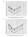
図6(a)は、本発明のSIMDプロセッサが双方向の一次元隣接PE間結合網のみを有する場合における、i=0のイタレーションにおけるサイクル毎でのPE間結合網の利用状況を示す。ここで、塗り潰した黒丸は、対応するPE(横軸)上で命令の実行が行われたことを表す。また、PEx→PEyの矢印は、PExとPEyとの間でデータ転送が発生したことを表す。なお、ここでは、グローバルメモリ40に対するロードアクセスの遅延を3サイクルと仮定している。したがって、PE1からPE2への矢印は3サイクルに跨っている。
FIG. 6A shows the usage status of the inter-PE connection network in each cycle in the i = 0 iteration when the SIMD processor of the present invention has only a bidirectional one-dimensional adjacent PE connection network. Here, the filled black circle indicates that the instruction is executed on the corresponding PE (horizontal axis). An arrow PEx → PEy indicates that data transfer has occurred between PEx and PEy. Here, it is assumed that the load access delay for the global memory 40 is three cycles. Therefore, the arrow from PE1 to PE2 extends over 3 cycles.
図6(b)は、i=0からi=7までの全部計8イタレーションにおける、サイクル毎のPE間結合網の利用状況を示す。図6(b)を参照すると、複数の同一方向の矢印間で交差が起きてない。このことは、PEアレイがシストリック動作を行った計21サイクルに亘って、PE間結合線を利用したデータ転送に関して、衝突が起きてないことを示す。なお、図6(b)において、サイクルPにおけるPExからPEyへの左→右(又は左←右)方向の矢印は、当該サイクルでのPEx→PEy(又はPEx←PEy)方向の隣接PE間結合線を利用してデータ転送が行われることを示す。また、図6(b)において、個々のイタレーション間を識別し易くするために、矢印及び塗り潰した丸印の明度を変更している。
FIG. 6 (b) shows the usage status of the PE network for each cycle in a total of 8 iterations from i = 0 to i = 7. Referring to FIG. 6B, no crossing occurs between a plurality of arrows in the same direction. This indicates that there is no collision regarding data transfer using the coupling line between PEs over a total of 21 cycles in which the PE array performs systolic operation. In FIG. 6B, the arrow in the left → right (or left ← right) direction from PEx to PEy in cycle P indicates the connection between adjacent PEs in the direction of PEx → PEy (or PEx ← PEy) in the cycle. Indicates that data transfer is performed using a line. Also, in FIG. 6B, the brightness of the arrows and filled circles is changed in order to make it easy to distinguish between individual iterations.
図5(c)及び図6では、グローバルメモリに対するPEによるロードアクセスの遅延を3サイクルと仮定した図を示している。一方、遅延が3よりも小さく、例えば、2である場合は、図7(a)のように、PE10に割当てていた命令をPE9に割当てればよい。また、ロードアクセス遅延が3よりも大きく、例えば、4である場合には、図7(b)のように、PE10に割当てていた命令をPE11に割当てればよい。
FIGS. 5C and 6 show diagrams assuming that the delay of the load access by the PE for the global memory is 3 cycles. On the other hand, when the delay is smaller than 3, for example, 2, the instruction assigned to PE10 may be assigned to PE9 as shown in FIG. When the load access delay is larger than 3, for example, 4, for example, the instruction assigned to PE10 may be assigned to PE11 as shown in FIG. 7B.
次に、実施形態に係るSIMDプロセッサの本実施例における効果について説明する。図8は、図5(a)のプログラムコードをCP30上で逐次的に実行した場合の擬似コードである。図8を参照すると、CADDは加算命令を表す。また、CLD及びCSTは、それぞれメモリロード命令及びメモリストア命令を表す。これらは、すべて「header」部が00の命令である。
Next, effects of the present example of the SIMD processor according to the embodiment will be described. FIG. 8 shows pseudo code when the program code of FIG. 5A is sequentially executed on the CP 30. Referring to FIG. 8, CADD represents an add instruction. CLD and CST represent a memory load instruction and a memory store instruction, respectively. These are all instructions whose “header” part is 00.
CP30のみを用いて、図5(a)のプログラムコードを実行した場合には、1回の繰り返し毎に約6サイクルを要することから、8回の繰り返しで合計48サイクルを要する。一方、図6(b)を参照すると、実施形態に係るSIMDプロセッサを利用することで、約21サイクルで処理が終了する。したがって、本発明によると、約2倍強の高速化を実現することができる。
When only the CP30 is used and the program code of FIG. 5 (a) is executed, approximately 6 cycles are required for each iteration, and therefore, a total of 48 cycles are required for 8 iterations. On the other hand, referring to FIG. 6B, the processing is completed in about 21 cycles by using the SIMD processor according to the embodiment. Therefore, according to the present invention, a speed increase of about twice or more can be realized.
なお、本実施例の場合、命令をPEアレイに分配するのに合計5サイクルを要することから、イタレーション回数が少ない場合における性能の向上は小さい。しかし、イタレーション回数を1000回とすると、命令をPEアレイに分配するのに要した5サイクルは無視することができる。また、本実施例では1イタレーション毎に1サイクルのスループットで実行できる。一方、図7を参照すると、CP30上で同一の処理を実行した場合には、1イタレーション毎に6サイクルかかる。したがって、本発明のSIMDプロセッサによると、約6倍の性能向上がもたらされる。
In this embodiment, since a total of 5 cycles are required to distribute the instructions to the PE array, the performance improvement is small when the number of iterations is small. However, if the number of iterations is 1000, the 5 cycles required to distribute the instructions to the PE array can be ignored. Further, in this embodiment, it can be executed with a throughput of one cycle for each iteration. On the other hand, referring to FIG. 7, when the same processing is executed on the CP 30, it takes 6 cycles for each iteration. Therefore, the SIMD processor of the present invention provides a performance improvement of about 6 times.
なお、上記の特許文献及び非特許文献の各開示を、本書に引用をもって繰り込むものとする。本発明の全開示(請求の範囲を含む)の枠内において、さらにその基本的技術思想に基づいて、実施形態ないし実施例の変更・調整が可能である。また、本発明の請求の範囲の枠内において種々の開示要素の多様な組み合わせないし選択が可能である。すなわち、本発明は、請求の範囲を含む全開示、技術的思想にしたがって当業者であればなし得るであろう各種変形、修正を含むことは勿論である。
It should be noted that the disclosures of the above patent documents and non-patent documents are incorporated herein by reference. Within the scope of the entire disclosure (including claims) of the present invention, the embodiments and examples can be changed and adjusted based on the basic technical concept. Various combinations and selections of various disclosed elements are possible within the scope of the claims of the present invention. That is, the present invention of course includes various variations and modifications that could be made by those skilled in the art according to the entire disclosure including the claims and the technical idea.
10、110、PE0~PE14 演算要素(PE:Processing Element)
11、111 命令バッファ(instb)
12、32、112 演算器(ALU)
20、120 ローカルメモリ(Local Memory)
30、130 制御プロセッサ(CP:Control Processor)
31 命令・データキャッシュ
33 アービタ(Arbiter)
35 プログラムカウンタ(PC:Program Counter)
40、140 グローバルメモリ(Global Memory)
50 大域アクセス調停部(Global Access Arbiter)
cm、mode、r0~r15、stop、sx、xy レジスタ
sel セレクタ 10, 110, PE0 to PE14 Processing element (PE)
11, 111 Instruction buffer (instb)
12, 32, 112 arithmetic unit (ALU)
20, 120 Local memory (Local Memory)
30, 130 Control processor (CP)
31 Instruction /data cache 33 Arbiter
35 Program Counter (PC: Program Counter)
40, 140 Global Memory (Global Memory)
50 Global Access Arbiter
cm, mode, r0 to r15, stop, sx, xy register sel selector
11、111 命令バッファ(instb)
12、32、112 演算器(ALU)
20、120 ローカルメモリ(Local Memory)
30、130 制御プロセッサ(CP:Control Processor)
31 命令・データキャッシュ
33 アービタ(Arbiter)
35 プログラムカウンタ(PC:Program Counter)
40、140 グローバルメモリ(Global Memory)
50 大域アクセス調停部(Global Access Arbiter)
cm、mode、r0~r15、stop、sx、xy レジスタ
sel セレクタ 10, 110, PE0 to PE14 Processing element (PE)
11, 111 Instruction buffer (instb)
12, 32, 112 arithmetic unit (ALU)
20, 120 Local memory (Local Memory)
30, 130 Control processor (CP)
31 Instruction /
35 Program Counter (PC: Program Counter)
40, 140 Global Memory (Global Memory)
50 Global Access Arbiter
cm, mode, r0 to r15, stop, sx, xy register sel selector
Claims (8)
- 制御プロセッサ(CP:Control Processor)と複数の演算要素(PE:Processing Element)とを備えたSIMD(Single Instruction Multiple Data)プロセッサであって、
前記複数のPEが前記CPから発行された単一の命令を実行するSIMD動作を行うとともに、
前記CPが前記複数のPEのそれぞれに対して相異なる命令又は相異なる命令及びデータを分配する命令・データ分配動作を行い、
前記複数のPEは、それぞれ、命令のソースオペランドが揃った後に前記命令・データ分配動作において前記CPから送付された命令を実行するシストリック動作を行うことを特徴とするSIMDプロセッサ。 A SIMD (Single Instruction Multiple Data) processor comprising a control processor (CP: Control Processor) and a plurality of computing elements (PE: Processing Element),
The plurality of PEs perform a SIMD operation to execute a single instruction issued from the CP,
The CP performs a command / data distribution operation for distributing different commands or different commands and data to each of the plurality of PEs,
The plurality of PEs each perform a systolic operation of executing an instruction sent from the CP in the instruction / data distribution operation after the source operands of the instruction are prepared. - 前記CPは、前記命令・データ分配動作において各PEに命令を分配するために、全PEに対する命令発行パスを逐次的かつ排他的に利用することを特徴とする、請求項1に記載のSIMDプロセッサ。 The SIMD processor according to claim 1, wherein the CP sequentially and exclusively uses an instruction issue path for all PEs in order to distribute instructions to each PE in the instruction / data distribution operation. .
- 前記シストリック動作において、前記複数のPEは、それぞれ、実行した演算命令の演算結果を他のPEに転送するとともに、他のPEから転送された演算結果を、前記命令・データ分配動作において送付された命令に対するソースオペランドとすることを特徴とする、請求項1又は2に記載のSIMDプロセッサ。 In the systolic operation, each of the plurality of PEs transfers the operation result of the executed operation instruction to another PE, and the operation result transferred from the other PE is sent in the instruction / data distribution operation. 3. The SIMD processor according to claim 1, wherein the SIMD processor is used as a source operand for an instruction.
- 前記シストリック動作において、前記複数のPEは、それぞれ、前記CPから送付されたデータを、前記命令・データ分配動作において送付された命令に対するソースオペランドとすることを特徴とする、請求項1又は2に記載のSIMDプロセッサ。 In the systolic operation, each of the plurality of PEs uses the data sent from the CP as a source operand for the instruction sent in the command / data distribution operation. The SIMD processor according to 1.
- 前記シストリック動作において、前記複数のPEのそれぞれによるグローバルメモリアクセスを調停し、グローバルメモリに対するアクセスの排他性を保証する大域アクセス調停部をさらに備えていることを特徴とする、請求項1乃至4のいずれか1項に記載のSIMDプロセッサ。 5. The system according to claim 1, further comprising a global access arbitration unit that arbitrates global memory access by each of the plurality of PEs in the systolic operation and guarantees exclusiveness of access to the global memory. The SIMD processor according to any one of the above.
- 前記複数のPEは、それぞれ、前記命令・データ分配動作中に動作を停止状態に保つためのフラグを格納するレジスタを備えていることを特徴とする、請求項1乃至5のいずれか1項に記載のSIMDプロセッサ。 The plurality of PEs each include a register for storing a flag for keeping the operation stopped during the instruction / data distribution operation. The SIMD processor described.
- 前記複数のPEは、それぞれ、前記SIMD動作と前記シストリック動作との間で動作を切り替えるためのフラグを格納するレジスタを備えていることを特徴とする、請求項1乃至6のいずれか1項に記載のSIMDプロセッサ。 The plurality of PEs each include a register that stores a flag for switching an operation between the SIMD operation and the systolic operation. The SIMD processor according to 1.
- 前記複数のPEは、それぞれ、前記CPから発行された命令を自身の命令バッファに格納するか否かを選択するセレクタを備えていることを特徴とする、請求項1乃至7のいずれか1項に記載のSIMDプロセッサ。 The plurality of PEs each include a selector for selecting whether or not to store an instruction issued from the CP in its own instruction buffer. The SIMD processor according to 1.
Priority Applications (1)
| Application Number | Priority Date | Filing Date | Title |
|---|---|---|---|
| JP2012501811A JP5708634B2 (en) | 2010-02-24 | 2011-02-23 | SIMD processor |
Applications Claiming Priority (2)
| Application Number | Priority Date | Filing Date | Title |
|---|---|---|---|
| JP2010-038976 | 2010-02-24 | ||
| JP2010038976 | 2010-02-24 |
Publications (1)
| Publication Number | Publication Date |
|---|---|
| WO2011105408A1 true WO2011105408A1 (en) | 2011-09-01 |
Family
ID=44506813
Family Applications (1)
| Application Number | Title | Priority Date | Filing Date |
|---|---|---|---|
| PCT/JP2011/053935 WO2011105408A1 (en) | 2010-02-24 | 2011-02-23 | Simd processor |
Country Status (2)
| Country | Link |
|---|---|
| JP (1) | JP5708634B2 (en) |
| WO (1) | WO2011105408A1 (en) |
Cited By (1)
| Publication number | Priority date | Publication date | Assignee | Title |
|---|---|---|---|---|
| JP2021157771A (en) * | 2018-10-18 | 2021-10-07 | シャンハイ カンブリコン インフォメーション テクノロジー カンパニー リミテッドShanghai Cambricon Information Technology Co., Ltd. | Network-on-chip data processing method and device |
Citations (6)
| Publication number | Priority date | Publication date | Assignee | Title |
|---|---|---|---|---|
| JPS63501530A (en) * | 1985-09-17 | 1988-06-09 | ザ・ジョンズ・ホプキンス・ユニバ−シティ | Wavefront array processor with linked memory |
| US4967340A (en) * | 1985-06-12 | 1990-10-30 | E-Systems, Inc. | Adaptive processing system having an array of individually configurable processing components |
| JPH0635878A (en) * | 1992-05-22 | 1994-02-10 | Internatl Business Mach Corp <Ibm> | Controller for single command plural data/ plural command plural data-processor-array |
| US5659780A (en) * | 1994-02-24 | 1997-08-19 | Wu; Chen-Mie | Pipelined SIMD-systolic array processor and methods thereof |
| JP2002175283A (en) * | 2000-12-05 | 2002-06-21 | Matsushita Electric Ind Co Ltd | Systolic array type computing unit |
| JP2008034953A (en) * | 2006-07-26 | 2008-02-14 | Kobe Univ | Image processing processor |
Family Cites Families (7)
| Publication number | Priority date | Publication date | Assignee | Title |
|---|---|---|---|---|
| EP0266300B1 (en) * | 1986-10-29 | 1994-12-07 | United Technologies Corporation | N-dimensional modular multiprocessor lattice architecture |
| JPH0668053A (en) * | 1992-08-20 | 1994-03-11 | Toshiba Corp | Parallel computer |
| CA2129882A1 (en) * | 1993-08-12 | 1995-02-13 | Soheil Shams | Dynamically reconfigurable interprocessor communication network for simd multiprocessors and apparatus implementing same |
| JP2657903B2 (en) * | 1994-11-29 | 1997-09-30 | 乾彌 呉 | Pipelined and contractile single instruction multiple data stream array processor and method |
| US5680597A (en) * | 1995-01-26 | 1997-10-21 | International Business Machines Corporation | System with flexible local control for modifying same instruction partially in different processor of a SIMD computer system to execute dissimilar sequences of instructions |
| JP3987784B2 (en) * | 2002-10-30 | 2007-10-10 | Necエレクトロニクス株式会社 | Array type processor |
| JP4477959B2 (en) * | 2004-07-26 | 2010-06-09 | 独立行政法人理化学研究所 | Arithmetic processing device for broadcast parallel processing |
-
2011
- 2011-02-23 WO PCT/JP2011/053935 patent/WO2011105408A1/en active Application Filing
- 2011-02-23 JP JP2012501811A patent/JP5708634B2/en active Active
Patent Citations (6)
| Publication number | Priority date | Publication date | Assignee | Title |
|---|---|---|---|---|
| US4967340A (en) * | 1985-06-12 | 1990-10-30 | E-Systems, Inc. | Adaptive processing system having an array of individually configurable processing components |
| JPS63501530A (en) * | 1985-09-17 | 1988-06-09 | ザ・ジョンズ・ホプキンス・ユニバ−シティ | Wavefront array processor with linked memory |
| JPH0635878A (en) * | 1992-05-22 | 1994-02-10 | Internatl Business Mach Corp <Ibm> | Controller for single command plural data/ plural command plural data-processor-array |
| US5659780A (en) * | 1994-02-24 | 1997-08-19 | Wu; Chen-Mie | Pipelined SIMD-systolic array processor and methods thereof |
| JP2002175283A (en) * | 2000-12-05 | 2002-06-21 | Matsushita Electric Ind Co Ltd | Systolic array type computing unit |
| JP2008034953A (en) * | 2006-07-26 | 2008-02-14 | Kobe Univ | Image processing processor |
Cited By (4)
| Publication number | Priority date | Publication date | Assignee | Title |
|---|---|---|---|---|
| JP2021157771A (en) * | 2018-10-18 | 2021-10-07 | シャンハイ カンブリコン インフォメーション テクノロジー カンパニー リミテッドShanghai Cambricon Information Technology Co., Ltd. | Network-on-chip data processing method and device |
| JP2021166034A (en) * | 2018-10-18 | 2021-10-14 | シャンハイ カンブリコン インフォメーション テクノロジー カンパニー リミテッドShanghai Cambricon Information Technology Co., Ltd. | Network-on-chip data processing method and device |
| JP7074833B2 (en) | 2018-10-18 | 2022-05-24 | シャンハイ カンブリコン インフォメーション テクノロジー カンパニー リミテッド | Network-on-chip data processing methods and equipment |
| JP7074832B2 (en) | 2018-10-18 | 2022-05-24 | シャンハイ カンブリコン インフォメーション テクノロジー カンパニー リミテッド | Network-on-chip data processing methods and equipment |
Also Published As
| Publication number | Publication date |
|---|---|
| JP5708634B2 (en) | 2015-04-30 |
| JPWO2011105408A1 (en) | 2013-06-20 |
Similar Documents
| Publication | Publication Date | Title |
|---|---|---|
| RU2427895C2 (en) | Multiprocessor architecture optimised for flows | |
| US8412917B2 (en) | Data exchange and communication between execution units in a parallel processor | |
| JP4156794B2 (en) | Method and apparatus for efficient synchronous MIMD operation using iVLIW inter-PE communication | |
| US9158575B2 (en) | Multithreaded processor array with heterogeneous function blocks communicating tokens via self-routing switch fabrics | |
| US11550750B2 (en) | Memory network processor | |
| EP1333381A2 (en) | System and method for processing image, and compiler for use in this system | |
| US8892620B2 (en) | Computer for Amdahl-compliant algorithms like matrix inversion | |
| JP2014501009A (en) | Method and apparatus for moving data | |
| KR102090885B1 (en) | Shift register with reduced wiring complexity | |
| JP4624098B2 (en) | Processor address generation unit | |
| JP2011523132A (en) | Execution engine | |
| US8024549B2 (en) | Two-dimensional processor array of processing elements | |
| US8190856B2 (en) | Data transfer network and control apparatus for a system with an array of processing elements each either self- or common controlled | |
| US8060726B2 (en) | SIMD microprocessor, image processing apparatus including same, and image processing method used therein | |
| US11782760B2 (en) | Time-multiplexed use of reconfigurable hardware | |
| JP5708634B2 (en) | SIMD processor | |
| KR100267092B1 (en) | Single instruction multiple data processing of multimedia signal processor | |
| JP5370352B2 (en) | SIMD type processor array system and data transfer method thereof | |
| JP5358315B2 (en) | Parallel computing device | |
| JP2024505440A (en) | Circuit and method for instruction execution dependent on trigger conditions | |
| Frijns et al. | Dc-simd: Dynamic communication for simd processors | |
| CN117009287A (en) | Dynamic reconfigurable processor stored in elastic queue | |
| Ito et al. | Reconfigurable instruction-level parallel processor architecture | |
| JP2006196015A (en) | Data processing processor and system |
Legal Events
| Date | Code | Title | Description |
|---|---|---|---|
| 121 | Ep: the epo has been informed by wipo that ep was designated in this application |
Ref document number: 11747368 Country of ref document: EP Kind code of ref document: A1 |
|
| WWE | Wipo information: entry into national phase |
Ref document number: 2012501811 Country of ref document: JP |
|
| NENP | Non-entry into the national phase |
Ref country code: DE |
|
| 122 | Ep: pct application non-entry in european phase |
Ref document number: 11747368 Country of ref document: EP Kind code of ref document: A1 |