WO2009117451A1 - Laser-based material processing methods and systems - Google Patents

Laser-based material processing methods and systems Download PDF

Info

Publication number
WO2009117451A1
WO2009117451A1 PCT/US2009/037443 US2009037443W WO2009117451A1 WO 2009117451 A1 WO2009117451 A1 WO 2009117451A1 US 2009037443 W US2009037443 W US 2009037443W WO 2009117451 A1 WO2009117451 A1 WO 2009117451A1
Authority
WO
WIPO (PCT)
Prior art keywords
laser
pulse
pulses
range
workpiece
Prior art date
Application number
PCT/US2009/037443
Other languages
French (fr)
Inventor
Lawrence Shah
Gyu Cheon Cho
Jingzhou Xu
Original Assignee
Imra America, Inc.
Priority date (The priority date is an assumption and is not a legal conclusion. Google has not performed a legal analysis and makes no representation as to the accuracy of the date listed.)
Filing date
Publication date
Application filed by Imra America, Inc. filed Critical Imra America, Inc.
Priority to JP2011500911A priority Critical patent/JP5826027B2/en
Priority to EP09721791.3A priority patent/EP2252426A4/en
Priority to CN200980109436.1A priority patent/CN102006964B/en
Publication of WO2009117451A1 publication Critical patent/WO2009117451A1/en
Priority to US12/641,256 priority patent/US8158493B2/en
Priority to US13/421,372 priority patent/US8785813B2/en
Priority to US14/319,845 priority patent/US20140312469A1/en

Links

Classifications

    • BPERFORMING OPERATIONS; TRANSPORTING
    • B23MACHINE TOOLS; METAL-WORKING NOT OTHERWISE PROVIDED FOR
    • B23KSOLDERING OR UNSOLDERING; WELDING; CLADDING OR PLATING BY SOLDERING OR WELDING; CUTTING BY APPLYING HEAT LOCALLY, e.g. FLAME CUTTING; WORKING BY LASER BEAM
    • B23K26/00Working by laser beam, e.g. welding, cutting or boring
    • B23K26/36Removing material
    • B23K26/38Removing material by boring or cutting
    • BPERFORMING OPERATIONS; TRANSPORTING
    • B23MACHINE TOOLS; METAL-WORKING NOT OTHERWISE PROVIDED FOR
    • B23KSOLDERING OR UNSOLDERING; WELDING; CLADDING OR PLATING BY SOLDERING OR WELDING; CUTTING BY APPLYING HEAT LOCALLY, e.g. FLAME CUTTING; WORKING BY LASER BEAM
    • B23K26/00Working by laser beam, e.g. welding, cutting or boring
    • B23K26/36Removing material
    • HELECTRICITY
    • H01ELECTRIC ELEMENTS
    • H01LSEMICONDUCTOR DEVICES NOT COVERED BY CLASS H10
    • H01L21/00Processes or apparatus adapted for the manufacture or treatment of semiconductor or solid state devices or of parts thereof
    • H01L21/02Manufacture or treatment of semiconductor devices or of parts thereof
    • H01L21/04Manufacture or treatment of semiconductor devices or of parts thereof the devices having at least one potential-jump barrier or surface barrier, e.g. PN junction, depletion layer or carrier concentration layer
    • H01L21/18Manufacture or treatment of semiconductor devices or of parts thereof the devices having at least one potential-jump barrier or surface barrier, e.g. PN junction, depletion layer or carrier concentration layer the devices having semiconductor bodies comprising elements of Group IV of the Periodic System or AIIIBV compounds with or without impurities, e.g. doping materials
    • H01L21/26Bombardment with radiation
    • H01L21/263Bombardment with radiation with high-energy radiation
    • H01L21/268Bombardment with radiation with high-energy radiation using electromagnetic radiation, e.g. laser radiation
    • BPERFORMING OPERATIONS; TRANSPORTING
    • B23MACHINE TOOLS; METAL-WORKING NOT OTHERWISE PROVIDED FOR
    • B23KSOLDERING OR UNSOLDERING; WELDING; CLADDING OR PLATING BY SOLDERING OR WELDING; CUTTING BY APPLYING HEAT LOCALLY, e.g. FLAME CUTTING; WORKING BY LASER BEAM
    • B23K26/00Working by laser beam, e.g. welding, cutting or boring
    • B23K26/02Positioning or observing the workpiece, e.g. with respect to the point of impact; Aligning, aiming or focusing the laser beam
    • B23K26/06Shaping the laser beam, e.g. by masks or multi-focusing
    • B23K26/062Shaping the laser beam, e.g. by masks or multi-focusing by direct control of the laser beam
    • B23K26/0622Shaping the laser beam, e.g. by masks or multi-focusing by direct control of the laser beam by shaping pulses
    • B23K26/0624Shaping the laser beam, e.g. by masks or multi-focusing by direct control of the laser beam by shaping pulses using ultrashort pulses, i.e. pulses of 1ns or less
    • BPERFORMING OPERATIONS; TRANSPORTING
    • B23MACHINE TOOLS; METAL-WORKING NOT OTHERWISE PROVIDED FOR
    • B23KSOLDERING OR UNSOLDERING; WELDING; CLADDING OR PLATING BY SOLDERING OR WELDING; CUTTING BY APPLYING HEAT LOCALLY, e.g. FLAME CUTTING; WORKING BY LASER BEAM
    • B23K26/00Working by laser beam, e.g. welding, cutting or boring
    • B23K26/08Devices involving relative movement between laser beam and workpiece
    • B23K26/082Scanning systems, i.e. devices involving movement of the laser beam relative to the laser head
    • BPERFORMING OPERATIONS; TRANSPORTING
    • B23MACHINE TOOLS; METAL-WORKING NOT OTHERWISE PROVIDED FOR
    • B23KSOLDERING OR UNSOLDERING; WELDING; CLADDING OR PLATING BY SOLDERING OR WELDING; CUTTING BY APPLYING HEAT LOCALLY, e.g. FLAME CUTTING; WORKING BY LASER BEAM
    • B23K26/00Working by laser beam, e.g. welding, cutting or boring
    • B23K26/08Devices involving relative movement between laser beam and workpiece
    • B23K26/083Devices involving movement of the workpiece in at least one axial direction
    • BPERFORMING OPERATIONS; TRANSPORTING
    • B23MACHINE TOOLS; METAL-WORKING NOT OTHERWISE PROVIDED FOR
    • B23KSOLDERING OR UNSOLDERING; WELDING; CLADDING OR PLATING BY SOLDERING OR WELDING; CUTTING BY APPLYING HEAT LOCALLY, e.g. FLAME CUTTING; WORKING BY LASER BEAM
    • B23K26/00Working by laser beam, e.g. welding, cutting or boring
    • B23K26/36Removing material
    • B23K26/362Laser etching
    • B23K26/364Laser etching for making a groove or trench, e.g. for scribing a break initiation groove
    • BPERFORMING OPERATIONS; TRANSPORTING
    • B23MACHINE TOOLS; METAL-WORKING NOT OTHERWISE PROVIDED FOR
    • B23KSOLDERING OR UNSOLDERING; WELDING; CLADDING OR PLATING BY SOLDERING OR WELDING; CUTTING BY APPLYING HEAT LOCALLY, e.g. FLAME CUTTING; WORKING BY LASER BEAM
    • B23K26/00Working by laser beam, e.g. welding, cutting or boring
    • B23K26/36Removing material
    • B23K26/40Removing material taking account of the properties of the material involved
    • BPERFORMING OPERATIONS; TRANSPORTING
    • B23MACHINE TOOLS; METAL-WORKING NOT OTHERWISE PROVIDED FOR
    • B23KSOLDERING OR UNSOLDERING; WELDING; CLADDING OR PLATING BY SOLDERING OR WELDING; CUTTING BY APPLYING HEAT LOCALLY, e.g. FLAME CUTTING; WORKING BY LASER BEAM
    • B23K2101/00Articles made by soldering, welding or cutting
    • B23K2101/36Electric or electronic devices
    • B23K2101/40Semiconductor devices
    • BPERFORMING OPERATIONS; TRANSPORTING
    • B23MACHINE TOOLS; METAL-WORKING NOT OTHERWISE PROVIDED FOR
    • B23KSOLDERING OR UNSOLDERING; WELDING; CLADDING OR PLATING BY SOLDERING OR WELDING; CUTTING BY APPLYING HEAT LOCALLY, e.g. FLAME CUTTING; WORKING BY LASER BEAM
    • B23K2103/00Materials to be soldered, welded or cut
    • B23K2103/50Inorganic material, e.g. metals, not provided for in B23K2103/02 – B23K2103/26
    • BPERFORMING OPERATIONS; TRANSPORTING
    • B23MACHINE TOOLS; METAL-WORKING NOT OTHERWISE PROVIDED FOR
    • B23KSOLDERING OR UNSOLDERING; WELDING; CLADDING OR PLATING BY SOLDERING OR WELDING; CUTTING BY APPLYING HEAT LOCALLY, e.g. FLAME CUTTING; WORKING BY LASER BEAM
    • B23K26/00Working by laser beam, e.g. welding, cutting or boring
    • B23K26/02Positioning or observing the workpiece, e.g. with respect to the point of impact; Aligning, aiming or focusing the laser beam
    • B23K26/06Shaping the laser beam, e.g. by masks or multi-focusing
    • B23K26/064Shaping the laser beam, e.g. by masks or multi-focusing by means of optical elements, e.g. lenses, mirrors or prisms
    • B23K26/0643Shaping the laser beam, e.g. by masks or multi-focusing by means of optical elements, e.g. lenses, mirrors or prisms comprising mirrors
    • BPERFORMING OPERATIONS; TRANSPORTING
    • B23MACHINE TOOLS; METAL-WORKING NOT OTHERWISE PROVIDED FOR
    • B23KSOLDERING OR UNSOLDERING; WELDING; CLADDING OR PLATING BY SOLDERING OR WELDING; CUTTING BY APPLYING HEAT LOCALLY, e.g. FLAME CUTTING; WORKING BY LASER BEAM
    • B23K26/00Working by laser beam, e.g. welding, cutting or boring
    • B23K26/02Positioning or observing the workpiece, e.g. with respect to the point of impact; Aligning, aiming or focusing the laser beam
    • B23K26/06Shaping the laser beam, e.g. by masks or multi-focusing
    • B23K26/064Shaping the laser beam, e.g. by masks or multi-focusing by means of optical elements, e.g. lenses, mirrors or prisms
    • B23K26/0648Shaping the laser beam, e.g. by masks or multi-focusing by means of optical elements, e.g. lenses, mirrors or prisms comprising lenses

Definitions

  • This disclosure relates generally to pulsed lasers and machining materials using high repetition rate pulsed lasers Description of the Related Art
  • the relatively large amount of ablated material ejected from a processing site may generally include one or more of liquid melt, relatively large quantities of solid mate ⁇ al, and vapor Fine distributions of particles, down to the nanometer scale (e g , 10 nm), may also be redeposited
  • a substrate may be coated with a sacrificial layer of material that is removed with the redeposited material after laser processing This process step may be used alone or in combination with post-processing of the substrate with various chemical solvents to remove the recast
  • process modifications reduce throughput and increase costs by adding additional processing steps and additional consumable materials
  • a preferred solution would eliminate the need for such debus removal
  • Low-k material can include material that has a dielectric constant that is less than the dielectric constant of silicon dioxide
  • low-k material can include dielectric materials such as doped silicon dioxide, polymeric dielectrics, etc
  • a method of laser processing a workpiece may comprise focusing and directing laser pulses to a region of the workpiece at a pulse repetition rate sufficiently high so that material is efficiently removed from the region and a quantity of unwanted material within or proximate to the region is reduced relative to a quantity obtainable at a lower repetition rate
  • the pulse repetition rate may be m a range from about 100 kHz to about 5 MHz in some embodiments of the method
  • a method of laser processing a workpiece may comprise focusing and directing laser pulses to a region of the workpiece at a pulse repetition rate sufficiently high so that heat accumulation within one or more materials is controlled in such a way that provides for rapid material removal, while limiting accumulation of redeposited material about the processed area
  • the method may allow control of a heat- affected zone (HAZ)
  • a method of laser processing a workpiece includes irradiating at least one material of the workpiece with laser pulses having a pulse width
  • the laser pulses may be focused onto spots in the at least one material
  • the focused spots may be relatively scanned with respect to the material at a scanning rate
  • the workpiece comprises a patterned region and a bare semiconductor wafer region
  • the patterned region can comprise at least one of a dielectric material and a metal material
  • the scanning rate used for removal of at least a portion of the patterned region is substantially less than the scanning rate used for removal of at least a portion of the bare wafer region
  • an overlap between adjacent focused spots is substantially greater for irradiation of the patterned region than for irradiation of the bare wafer region
  • the overlap for irradiation of the patterned region may be greater than about 95% in some cases
  • At least a portion of material withm the patterned region is modified using a pulse width in a range of about 100 ps to about 500 ps. In some embodiments, at least a portion of material within the semiconductor wafer region is modified using a pulse width in a range of about 100 fs to about 10 ps
  • At least one implementation includes an ultrashort pulse laser system suitable for carrying out embodiments of the above methods of laser processing
  • At least one embodiment includes an ultrashort pulse laser system that comprises at least one of a fiber amplifier or a fiber laser
  • At least one embodiment includes an ultrashort pulse laser system configured as an "all-fiber" design
  • a pulsed laser system provides a pulse width of at least one pulse that is less than about 10 ps In some embodiments, a pulse width of at least one pulse is less than about a few nanoseconds, for example a sub-nanosecond pulse
  • the method comprises directing laser pulses toward at least one material of a multi-material workpiece
  • the laser pulses can have a pulse width in a range from tens of femtoseconds to about 500 picoseconds and a pulse repetition rate of a few hundred kHz to about 10 MHz
  • the workpiece can comprise both a pattern and a semiconductor wafer, and the pattern can comprise at least one of a dielectric material and a metal material
  • the method can also include focusing the laser pulses into lasers spots having spot sizes m a range from a few microns to about 50 ⁇ m (1/e 2 ) and positioning the laser spots relative to the at least one material at a scan speed such that an overlap between adjacent focused spots for removal of material from at least a portion of the pattern is substantially greater than an overlap between adjacent focused spots for removal of material from at least
  • Embodiments of a method of processing a workpiece that comprises a pattern and a semiconductor wafer are provided
  • the pattern can comprise at least one of a dielectric material and a metal material
  • the method includes modifying at least a portion of the pattern with a laser pulse comprising a pulse width in the range from about 100 ps to about 500 ps and modifying at least a portion of the semiconductor wafer with a laser pulse comprising a pulse width in a range from about 100 fs to about 10 ps
  • Embodiments of a method of laser processing a multi-material workpiece having a semiconductor material comprise focusing and directing laser pulses to a region of the workpiece at a pulse repetition rate in a range from about 100 kHz to about 10 MHz and at a repetition rate sufficiently high so that material is efficiently removed from the region and a quantity of unwanted material within or proximate to the region is limited relative to a quantity obtainable at a lower repetition rate below about 100 kHz
  • the method comprises repeatedly irradiating at least one target material of the workpiece with focused laser pulses at a scan rate and a pulse repetition rate
  • the repetition rate may be in a range of at least about a few hundred kHz to about 10 MHz, and the scan rate may be in a range of about 0 2 m/s to about 20 m/s
  • at least some of the focused laser pulses have a non-zero spatial overlap factor with at least one other pulse, a pulse width less than about J ns, a pulse energy in a range of about 100 nJ to about 25 ⁇ j.
  • a focused (1 /e 2 ) spot size in a range of about 5 ⁇ m to about 50 ⁇ m, and a fluence in a range of about 0 25 J/c ⁇ T to about 30 J/c ⁇ T at the target material
  • Embodiments of method of processing a multi-material workpiece aie disclosed
  • the workpiece can comprise a semiconductor material and a pattern, and the pattern can comprise at least one of a dielectric material and metal material
  • the method comprises irradiating the workpiece with a series of laser pulses, with at least two pulses of the series having different characteristics that are applied to different materials of the workpiece
  • the method also comprises controlling heat-affected zone (HAZ) such that at least one HAZ generated during removal of at least one of the dielectric material and the metal material is increased depthwise relative to at least one HAZ generated during removal of a portion of the semiconductor material
  • HAZ heat-affected zone
  • Embodiments of a method of processing a workpiece comprising both a pattern and a semiconductor wafer region are disclosed
  • the pattern can comprise a dielectric material and a metal material
  • the method comprises modifying at least a portion of the pattern with focused laser pulses, with at least one focused pulse comprising a pulse width m a range of about 100 fs to about 500 ps
  • the method also includes accumulating sufficient heat in the portion of the pattern to avoid delamination of the dielectric material from the metal material
  • the laser-based system comprises a source of optical pulses and an optical amplification system configured to amplify a pulse from the source to a pulse energy of at least about 1 ⁇ J and to generate output optical pulses having at least one pulse width in a range from about 500 fs to a few hundred picoseconds
  • the system may also include a modulation system, comprising at least one optical modulator, configured to adjust a repetition rate of the output optical pulses to be within a range from about 100 kHz to about 10 MHz, and a beam delivery system configured to focus and deliver pulsed laser beams to the workpiece such that a pulsed beam is focused into a spot size (l/e ⁇ ) in a range from about 15 ⁇ m to about 50 ⁇ m
  • the system may also include a positioning system configured to scan the beams relative to the one or
  • Embodiments of a laser-based system for scribing, dicing, cutting, or processing of a multi-material workpiece having a semiconductor material comprise a source of optical pulses and an optical amplification system configured to amplify a pulse from the source and to generate output pulses having at least one pulse width in a range from tens of femtoseconds to about 500 picoseconds
  • the system can also include a modulation system, including at least one optical modulator, configured to provide a repetition rate of the output optical pulses to be in a range from at least about 1 MHz to less than about 100 MHz
  • the system also can include a beam delivery system configured to focus and deliver pulsed laser beams to the workpiece, such that a pulsed beam is focused into a spot size (1/e 2 ) of at least about 5 microns, and a positioning system configured to scan the beams at a scan rate that produces a spot overlap on or within the one or more mate ⁇ als
  • the system comprises a pulsed laser system configured to repeatedly irradiate at least a portion of the material with focused laser pulses at a scan rate and a pulse repetition rate
  • the repetition rate can be m a range of about 100 kHz to about 5 MHz and sufficiently high to efficiently remove a substantial depthwise portion of material from a target location and to limit accumulation of unwanted material about the target location
  • the system can also include a beam delivery system configured to focus and deliver the laser pulses, and a positioning system configured to position the laser pulses relative to the semiconductor substrate at the scan rate
  • the positioning system can comprise at least one of an optical scanner and a substrate positioner
  • a controller is configured to be coupled to the pulsed laser system, the beam delivery system, and the positioning system The controller can be configured to control a spatial overlap between adjacent focused laser pulses during processing of the workpiece at the repetition rate
  • FIGs I A-I C schematically illustrate top and cross-sectional views representing an embodiment of a multiple pass laser-based method for material removal
  • Figs I D-] E schematically illustrate cross-sectional views representing a relation between machining depth and formation of unwanted re-deposited material after N passes
  • Fig I E is a schematic representation of a result obtainable with at least one embodiment of a pulsed laser system
  • Fig IF schematically illustrates an embodiment of a laser system suitable for processing a workpiece with laser pulses
  • Figs IG-I to 1 G-3 schematically illustrate examples of portions of patterned wafers
  • Fig I G-I illustrates a wafer having several die
  • Fig 1 G-2 illustrates an expanded view of a portion of the wafer of Fig I G-I
  • Fig 1 G-3 illustrates a cross sectional side-view of a portion of the wafer
  • FIGs 2A-2B schematically illustrate embodiments of a system for processing a workpiece with laser pulse trains
  • FIG 3 schematically illustrates another embodiment of a system for processing a workpiece with laser pulse trains
  • FIG 4A schematically illustrates yet another embodiment of a system for processing a workpiece with laser pulse trains
  • Fig 4B schematically illustrates an embodiment of a large mode area fiber comprising a core doped with rare earth ions that can be used in a fiber amplifier or in a laser pumped by a multimode pump source
  • Fig 5 schematically illustrates a further embodiment of a system for processing a workpiece with laser pulse trains, the system having feedback and controls based on process and/or target information
  • Figs 6A and 6B show a schematic representation and a photograph, respectively, illustrating an experimental system corresponding to an embodiment for processing a workpiece with laser pulse trains
  • FIG. 7 schematically illustrates one example technique for quantifying processing quality so as to obtain an approximation of an ablated volume and a redeposited volume proximate to a processing location
  • Figs 7A-7F show example scanning electron microscope (SEM) cross sections obtained from silicon samples, wherein the experimental results were obtained by varying laser processing parameters of the example system of Figs 6A and 6B
  • Fig 8 is a plot showing examples of ablated cross-sectional area versus re- deposited cross sectional area as a function of scan speed and repetition rate
  • Fig 9 is a plot of further illustrating examples of cross-sectional area versus scan speed, normalized for average power and spatial overlap of spots
  • Figs lOA-1 and 10A-2 show example SEM cross-sections, wherein a quantity of re-deposited material is sufficiently low such that conventional ultrasonic cleaning is effective for further debris removal, the result being applicable to. for example, thm-wafer dicing and similar applications
  • Fig 1OB is a plot of a ratio of ablated depth to recast height corresponding to the data shown m Figs lOA-1 and IOA-2
  • Figs 11 A-1 1 C show example SEM cross-sections comparing results of single and double pulse processing
  • Figs 1 ID-I IE are plots showing the ratio of ablated depth to recast height, corresponding to the SEM images of Figs 11 A-1 1 C
  • Figs 12 A- 12B are SEM images showing a portion of a wafer cut (diced) using an embodiment of a pulsed laser system, and a result obtained after conventional ultrasonic cleaning
  • Figs 13A-1 -13A-3 are SEM images showing results obtained with various repetition rates and scan speeds using about 200 ps pulse widths
  • Figs 13A-4-13A-5 are plots showing weighted ablated cross-sectional area (in square microns) and a ratio of ablated depth to recast height, respectively, corresponding to the data shown in Figs 13A-1 -13A-3
  • Figs 14 and 14A-1 and 14A-2 schematically illustrate various examples of configurations used to test die strength of semiconductor devices
  • Figs 14B and 14C are plots illustrating examples of die strength measurements obtained after processing samples with ultrashort pulses from the example experimental system illustrated in Figs 6A and ⁇ B
  • Figs 15A-15D show examples of SEM images, and cross sections of samples scribed and/or cut with ultrashort pulses generated with the example experimental system of Figs 6A and 6B
  • Figs 16A-16D show examples of SEM images illustrating femtosecond and picosecond scribing results
  • Fig 17 illustrates experimental test results showing die strength of silicon dies cut with 500 fs compressed pulses or 300 ps uncompressed pulses
  • Fig 17 also includes published nanosecond laser results and mechanical test results for comparison Circles are used to show results for dies in tension, and squares are used to show results for dies in compression Average values (and error bars) corresponding to the experimental test results are offset horizontally (to the right) of the individual experimental test results with 500 fs and 300 ps pulses
  • target mate ⁇ al generally refers to material in or on at least one region of a workpiece that is to be modified by one or more laser pulses
  • the target material may comprise multiple materials having different physical properties
  • repetition rate generally refers to a rate at which laser pulses are delivered to a target material during laser processing of the mate ⁇ al
  • the rate may correspond to the rate at which pulses are generated by a laser source, but the rate may also be reduced relative to the source rate in embodiments where, for example, a pulse or group of pulses is gated and delivered to the target material
  • debris is not limiting, and geneially refers to unwanted accumulation of mate ⁇ al within or proximate a localized region
  • Debris may result from laser-material interaction and/or a heat affected zone (HAZ) Recast, slag, redeposit and other related terms are also well known in the art
  • HAZ heat affected zone
  • a heat affected zone includes mate ⁇ al heated and cooled fast enough to form molten material, and the extent of the region depends, among other factors, on the pulse duration and various material parameters Short pulses, particularly ultrashort pulses, are known to localize the heat and reduce the dimension of a heat-affected zone Overview
  • Embodiments are generally applicable for laser processing a workpiece, and particularly for micromachining applications
  • various embodiments are applicable to cutting, dicing, scribing, and/or engraving semiconductor substrates to form features having a typical lateral dimension of about 1 micron to about 100 microns and a depth from a few microns to hundreds of microns
  • certain embodiments may be utilized for fabrication of precise trenches and grooves in a variety of materials
  • Extremely precise trenches m silicon are required for a va ⁇ ety of microelectronic applications
  • the preferred method for micro-fluidic device fabrication is via lithographic processing, often involving several cycles of ultraviolet (UV) light exposures that is followed by a solvent etch
  • Femtosecond lasers are capable of directly machining blind and through holes of modest aspect ratio (1 10-1 100, depending upon substrate material, laser parameters and hole diameter)
  • ultrashort laser pulses offer important advantages relative to conventional nanosecond lasers reduced HAZ, reduced residual stress, less sensitivity to variations in material ablation thresholds Furthermore, it is well established that relatively high processing rates can be achieved by scaling laser average power (assuming fluence on the target is greater than the material ablation threshold) and using high speed multi-pass beam scanning Ultrashort laser processing is also generally recognized as a suitable approach for reduction of slag, residue, melt formations or other unwanted byproducts of laser-material interaction However, it is also well established that the use of ultrashort pulses alone cannot guarantee improved quality Many early experiments were carried out m vacuum which simplified processing Citations to various publications, patents, and published patent applications relating to material processing with ultrashort pulses, micromachining of one-or more of semiconductor, metal, or dielectric materials used in semiconductor device manufacturing, laser-material interaction mechanisms, and systems for micromachining may be found in the priority U S provisional patent applications
  • Embodiments disclosed herein may be utilized to form high aspect ratio features m a material, wherein a depth to width ratio is large
  • Such features sometimes referred to as grooves or trenches, may be formed by controllably remo ⁇ ing material from a workpiece surface
  • the material may be removed by repeatedly scanning focused laser pulses over a target region with a mechanism to position the target material and/or the laser pulses relative to each other
  • Some embodiments may be utilized for laser cutting of materials, particularly semiconductor substrates Such embodiments may also include the formation of high-aspect ratio features as part of the process For example, thm wafer dicing advantageously may use clean and precise cuts to separate wafer die without damaging nearby circuitry or structures The wafer may be diced using focused laser pulses to cut through the entire wafer, perhaps changing the depthwise position of focus during cutting in some embodiments Alternatively, laser pulses may form a high aspect ratio feature, for example, a narrow and deep cut of pre-deteimmed depth A thin depthwise portion of remaining material is then separated using a non-laser method In any case, it may be advantageous for debris and contamination to be sufficiently well controlled
  • Figs IA- 1 C are schematic illustrations showing a portion of a process for laser-based material modification Examples of focused laser spots 1000-a, 1001 -a are shown with an overlap factor which may be a small fraction of a spot diameter in some embodiments
  • the overlap factoi may be different than schematically shown in Fig I A
  • the overlap factor may be approximately the same from spot to spot (e g , as schematically illustrated in Fig I A) or the overlap factor may differ from spot to spot
  • Different laser passes may utilize different overlap factors (and/or spot shapes, spot diameters, etc )
  • some adjacent spots can substantially overlap (e g , having an overlap factor that is a small fraction of a spot diameter) or some adjacent spots can be spaced apart (e g , having an oveilap factor that is approximately the same, or larger, than the spot diameter)
  • an overlap factor may be selected to provide machined features with, for example smooth straight edges, or selected to affect heat accumulation within a region In such embodiments, the
  • the spots may be applied to target material of a workpiece with one pass or with multiple passes, for example with a scanning mechanism (not shown)
  • Figs 1 A- IC the upper illustrations schematically show the first pass of the laser pulses (Passl ), and the lower illustrations show the N th pass of the laser pulses (Pass N)
  • any suitable number N of processing passes may be used, for example, J , 2, 5, 10, 100, 250, 700, 1000, or more passes
  • a simplified top schematic view of a target region is shown in Fig IB, showing a region where material was removed with the circular spots 1000-a, 1001 -a
  • the region has a lateral dimension on the order of a spot diameter, although it is generally known that with ultrashort pulses it is possible to controllably remove material over a region smaller than a spot dimension, as taught in, for example, U S Patent No 5,656,186
  • the region where material is removed is schematically shown as a rectangle, although at
  • the features may be formed with laser spots to remove a depthwise portion of the target material, for example, about 0 5 ⁇ m or a few microns in some embodiments
  • a relatively small depth-portion 1000-c is removed (see upper illustration in Fig 1 C)
  • N passes a feature may be formed having a desired depth and/or spatial profile
  • the material may be cleanly severed (e g , cut all the wa ⁇ through the material, sometimes called "breakthrough")
  • the number of passes N may be 1 , 2, 3, 4, 5, 10, 25, 100, 250, 500, 750, 1000, 1500, 2000, 5000, or more
  • the number of passes may be selected based on factors including, for example, the desired depth and/or spatial profile of the feature, the mate ⁇ al(s) forming the work
  • Fig IB schematically shows a simple linear/rectangular machined pattern as viewed from above the workpiece
  • machined features may be circular, elliptical, interleaved, spiral or other arbitrary shapes that will be formed by programming the relative positions of the laser pulse source and target material (e g , with a scanning mechanism, as will be further illustrated below)
  • the focused spot distributions may be non-circular and/or may have Gaussian or non-Gaussian spot profiles
  • various shapes may be formed as a function of depth, for example tapered, stepped, and/or curved features wherein the width of the feature varies with depth in a pre-determined manner, or approximately so
  • High aspect ratio features may be formed alone or in combination with other features, and may be connected to a region having a lower aspect feature, for example a large diameter hole
  • Some parameters of interest for embodiments of "trench digging" or other applications may include, for example, the shape, depth, and quality of the trench
  • redeposited material commonly called recast or slag
  • recast or slag may be formed at or very near the edges of the narrow trenches The quantity of redeposited material generally increases with increased machining depth
  • Figure I D schematically illustrates a cross-sectional view of a machined feature 1001 -c having a depth (as in Figs 1 A-I C), but having significant redeposited material 1005-a
  • the redeposited material 1005-a may be above a surface of the workpiece and/or within the machined feature 1001 -c
  • a baseline of the non-processed substrate is depicted as the dashed lines in Figs ID and IE
  • the redeposited material may also accumulate within a feature or target region, for example withm a depth of several microns below the baseline (see Fig ID)
  • Figure IE is representative of an example result obtainable with pulsed laser embodiments, wherein, for a fixed number of passes N, accumulation of redeposited material 1005-b is reduced (compared to the result schematically shown in Fig ID) As illustrated in Fig IE, the cross sectional area of redeposited material is reduced (relative to Fig ID) and/or the type of material deposited is in the form of fine particles as opposed to molten material of a larger dimension For example, in some embodiments, such a result is obtainable by increasing the laser repetition rate and, in this example, holding other laser parameters approximately constant
  • the accumulation of the redeposited material may be reduced within the target region, proximate to the target region, or both
  • the nature of the redeposited material e g , the size distribution of the particles
  • results from machining experiments on silicon substrates showed a surprising result increasing the laser repetition rate of laser pulses from about 200 kHz to about 1 MHz, while maintaining approximately constant laser pulse energy, focal spot size, and pulse duration, produced an increase in the volume of material removed relative to the amount of material redeposited
  • the experiments were carried out using a fiber-based ultra-short chirped pulse laser system
  • pulse repetition rates of several hundred kHz up to several MHz may provide a significant improvement in processing quality For example, in certain applications, additional processing steps may not be required to remove redeposited material
  • Embodiments may therefore decrease the quantity of slag and/or other unwanted material (and/or change the nature of the redeposited material), while providing for a desired shape, depth, and/or width of the features
  • high repetition rate processing affected the nature and quantity of re-deposited material
  • a measure of quality may be the depth and/or volume of a machined feature relative to a peak height, average height, and/or volume of redeposited material
  • Another example measure of quality may be the feature depth relative to the total volume of redeposited material
  • Suitable measures of quality may be obtained with cross-sectional samples or volumetric quantification of an affected region
  • Various tools may be used to quantify performance, for example, surface metrology tools such as white light interferometers, Atomic Force Microscopes (AFMs), or similar tools (available from, for example, Veeco Instruments Inc , Woodbury, New York)
  • the tools may provide for improved measurement accuracy and precision, with capability for automated or semi- automated operation
  • the commercially available tools have proven capability for measuring surface roughness of a sample and also larger volumes of mate ⁇ al, and AFMs may be used to quantify structure of the depthwise features, for example
  • quantification of the volume of redeposited mate ⁇ al may be a useful measure, and may be combined with cut quality as an overall figure of merit
  • Various embodiments are particularly applicable for processing operations where high efficiency is desirable, and wherein accumulation of redeposited mate ⁇ al is detrimental or otherwise undesirable
  • micromachining may include laser scribing, dicing, or similar processing of semiconductor wafers, which may be bare or patterned Scribing and dicing are two applications with a recognized need Scribing typically removes one or more layers of multiple materials supported on a silicon substrate The die of a wafer may then be separated with a mechanical dicer With decreasing of silicon substrate thickness to below 100 ⁇ m, for example 50 ⁇ m, an increased need for laser based dicing of the substrates has developed However, in some implementations, rapid laser processing speeds are required to provide justification to replace conventional mechanical dicing Moreover, in some implementations, undesirable thermal effects are to be reduced or avoided to assure reliability of subsequent packaging processes
  • Figs 1 G-I (not to scale) schematically illustrates an example of a patterned semiconductor wafer 120 having several die arranged in rows and columns with streets 127 therebetween
  • the wafer is typically laser scribed, and cut using a dicing saw
  • the thickness decreases below about 100 ⁇ m. for example 50 ⁇ m or 75 ⁇ m, mechanical dicing becomes more difficult Therefore, it is desirable to use laser dicing to reduce or eliminate mechanical dicing
  • Fig 1 G-2 schematically illustrates an example portion 125 of the wafer 120
  • dicing is to be carried out in region 127-B along the streets
  • the region may include several materials and bare wafer portions
  • the circuit features shown in the streets for example high-density grid layer 129. may be utilized for electrical or other functional tests prior to dicing
  • the regions adjacent to street 127 contain high density active circuits, interconnects which may include solder balls, or other combinations
  • the dicing or scribing is to be carried out to cleanly cut the wafer without causing damage to circuitry, without introducing significant debris or heat affected zone (HAZ), and should provide for sufficient die strength
  • FIG 1 G-3 schematically illustrates a cross sectional side-view 129-1 of a portion of the wafer, the fine grid area 129 of Fig 1 G-2
  • the grid may be covered with one or more of dielectric and metal materials
  • Workpiece materials in the streets may include, but are not limited to, metals, inorganic dielectrics, organic dielectrics, semiconductor materials, low-k dielectric materials, or combinations thereof
  • the combinations of materials may be arranged in widel> varying spatial patterns and/or stacked in depth
  • microelectronic circuits may comprise portions having alternating layers of copper and low-k mate ⁇ al, covered by an overlying passivation layer
  • Other combinations and/or configurations of mate ⁇ als are possible
  • scribing and/or dicing of 50 ⁇ m thick or similar substrates may be carried out with a focused spot size of at least 15 ⁇ m, and with a spot size in the range of about 15-50 ⁇ m in some embodiments
  • spot sizes may be used such as, for example, a few microns (e g , about 3 microns m one case)
  • spot sizes in a range from about 1 micron to about 5 microns are used
  • the quantity of material removed is generally determined by one or more factors including the scan speed, spot overlap, repetition rate (pulses per second delivered to surface), pulse energy, and spot diameter
  • sufficient overlap between adjacent spots on the surface provides for cutting or scribing a pattern of relatively uniform width
  • relatively high pulse energy of at least a few microJoules with a spot size of about 15 ⁇ m will typically result m ablation within a region having diameter about 15-20 ⁇ m
  • a scanning system for example a galvanometer based mirror
  • ultrashort pulses may be applied at a high rate and reduced motion speed to induce thermal effects similar to non-ultrashort pulses
  • one or more of pulse energy, repetition rate, speed, and pulse width may be adjusted
  • available pulse energy will be at least about 5 ⁇ j
  • repetition rates will be adjustable up to about 10 MHz
  • beam speed at the surface may be in a range of about 0 1 m/sec up to about 10 m/sec
  • pulse widths provided within a range from below 1 picosecond up to a few nanoseconds
  • the scan speed, pulse energy, repetition rate (rate at which pulses impinge the surface), pulse width, and spot size are preferably adjustable over a wide range, for example at least 2 1 in some embodiments
  • One or more such parameters, for example the pulse width, speed, and repetition rate, may be adjustable over more than a 10 1 range
  • Other adjustable ranges are possible in other embodiments
  • a typical multimate ⁇ al device for example a patterned wafer, may include conductor, dielectric, and semiconductor materials stacked in depth Processing of a typical multimate ⁇ al device may be carried out at, for example, a 1 MHz repetition rate, a spot size of about 40 ⁇ m, and at motion speeds producing overlap between about 75% to more than 99% between adjacent spots
  • the scan speed may be controlled in such a way that tailors the heat accumulation to facilitate material removal while simultaneously limiting debris and controlling HAZ
  • removal of metal and dielectric layers may be carried out at a scan speed substantially slower than a scan speed used for removal of bare silicon
  • the overlap between adjacent spots for removal of at least one of a metal and dielectric may be greater than an overlap for bare wafer processing (e g , at least about ten-times greater in some embodiments)
  • a focused spot size in the range of about ] 5-40 ⁇ m, and typically about 30-40 ⁇ m, provides for high throughput in some cases
  • the width of street 127 may be reduced in certain wafer designs, for example to a few ten of microns
  • a corresponding reduction in spot size from certain preferred values above e g about 40 ⁇ m in some cases
  • a cutting path 127-b within street 127 is illustrated, the cutting path 127-b centered on the street region in this example
  • wafer scribing and breaking may be carried out with a combination of a laser, for example a nanosecond pulsed laser, and a dicing saw
  • the nanosecond laser may, in some implementations, scribe two lines at approximately equal distance from the center of the street A dicing blade centered on the street is used to cut through the remaining wafer, thereby producing individual die
  • Embodiments desc ⁇ bed herein may also be used to modify material along any path (e g , a pre-determmed path for the wafer), and/or may be used in various combinations (e g , with a dicing saw)
  • the material to be modified or processed may comprise metal, dielectrics including low-k materials, and/or semiconductors
  • processing of ultra-thin wafers such as, for example 50 ⁇ m thick wafers, can be carried
  • requirements for precision positioning may increase, but total pulse energy may be decreased It is well known that a decreasing spot size at a particular wavelength results in a decreased depth of focus (DOF)
  • DOF depth of focus
  • the DOF decrease generally varies as the square of the spot size If processing over a large depth range is required various well known methods and systems for dynamic focusing, or improvements thereof, may be applied in some cases
  • the spot size decreases from 50 ⁇ m to 5 ⁇ m the DOF decreases by 100-fold
  • the total pulse energy to achieve a given fluence over a spot area decreases as the square of the spot diameter
  • much lower maximum pulse energy may be used for smaller spot sizes, and a maximum pulse energy may be, for example, about 100 nJ, or up to about 1 ⁇ J, for processing of various dielectric, conductor, and semiconductor materials
  • a smaller spot size may lead to some considerations for motion control also Reduced scan speeds may be utilized in some embodiments, but a requirement for precision positioning may also be increased
  • pulse energy and speed may be scaled downward while processing at a given fluence and repetition rate
  • corresponding scan speed is on the order of 10 mm/sec
  • the fluence may be obtained with pulse energy may be scaled down from a range of at least a few microjoules (e g 5 ⁇ j) to below 100 nanojoules (e g 50 nJ) as a result of a 10-fold decreased spot size
  • the repetition rate may be increased to tens of MHz, and with relatively low pulse energy for certain micromachining operations
  • some cutting or scribing applications may require selective removal of a single layer of material, or a few layers, with relatively low fluence
  • Fig 1 G-3 one of more layers are schematically represented by shaded regions (not necessarily to scale), and may comprise dielectric and/or metal materials
  • the underlying bare wafer (not shaded) is processed by the laser after modification of the overlying layers in certain processing applications
  • thermal processing e g , heat accumulation
  • HAZ sufficient heat affected zone
  • reduced HAZ associated with ultrashort pulses may be beneficial for cutting through the wafer for singulation of die
  • nanosecond pulses are used both to remove layers and for dicing the silicon wafer performance may be insufficient or unpredictable
  • weak die strength and various other material issues are caused by excessive HAZ caused by nanosecond pulses
  • Femtosecond pulse irradiation in some implementations provides a shallow HAZ, but little interaction with underlying layers of a device occurs as a result of the ultrashort pulse width
  • the femtosecond heating process is almost instantaneous, confines HAZ to a limited thickness, and does not substantially affect layers disposed below modified material Much smoother and predictable surface morphology is achievable in certain such implementations
  • multiple lasers may be utilized, and configured m an integrated laser system having multiple sources, or as a source having adjustable pulse widths
  • a relatively long pulse width for example hundreds of picoseconds and up to a few nanoseconds, may be utilized to increase HAZ for processing a first depthwise portion of a workpiece, and particularly for removing low-k layers and/or other metals and/or other dielectrics
  • metals may include, but are not limited to, copper, aluminum, and/or gold
  • Dielectric materials may include, but are not limited to, silicon dioxide, silicon nitride, and/or various organic or inorganic materials The arrangement of the dielectric and/or metal materials may vary in three-dimensions as schematically illustrated in the examples shown m Figs 1 G-I to ⁇ G-3
  • ultrashort pulses may be used to process a second depthwise portion of the workpiece, with generation of negligible HAZ
  • femtosecond pulses are utilized for at least cutting through the entire wafer, or a substantial fraction of the wafer, and particularly for cutting very thin wafers, for example wafers having thickness of 100 ⁇ m or less
  • at least a portion of the processing of metals and/or dielectrics may also be earned out with femtosecond pulses
  • a single laser source may be utilized Adjustment of laser parameters may balance heat generation within a processing region and transfer of heat outward from the region Delammation and/or unwanted thermal stress are then reduced or avoided
  • a picosecond pulse width may be utilized to remove a low-k material
  • at least one pulse may be in the range of about 100 ps to about 500 ps, about 100 ps to 250 ps, or in the range of about 200 ps to 500 ps
  • at least one pulse may have a pulse energy may in the range of about 2 ⁇ j to 10 ⁇ j over a spot diameter of 30-40 ⁇ m, corresponding to a fluence at least about 0.15 J/cm 2 , for example.
  • Such examples of pulse widths and fluence can generate sufficient HAZ for processing metal and dielectrics, and within a period of time to provide material modification, (e.g.: melting and removal) of multiple layers.
  • any region of melted material is also sufficiently shallow (e.g.: not too deep) so that unwanted cracking, surface roughness and/or voids in the HAZ are reduced or avoided.
  • other pulse widths, pulse energies, spot diameters, and fluences may be used.
  • the width of street 127 may be reduced.
  • Embodiments of the laser system may then be configured with a reduced spot size for processing in a narrowed region.
  • the pulse energy can then be reduced while maintaining a given fluence.
  • a relatively high fluence may be selected for processing and may be advantageous for processing of various metals and dielectrics.
  • Fig. IF schematically illustrates an embodiment of a system 100 suitable for processing a workpiece with laser pulses.
  • the system 100 comprises a laser system 104 that is operatively coupled to a controller 1 14 and scanning system 106.
  • the laser system 104 is configured to output laser pulses that comprise one or more ultrashort pulses (USP).
  • USP ultrashort pulses
  • the laser system 104 comprises a USP laser.
  • the system 100 will provide for adjustment of certain pulse parameters over a substantial range. Such parameters may include one or more of pulse energy, pulse repetition rate, pulse width, spot diameter, overlap of adjacent spots, and scan speed.
  • pulses may be generated at an adjustable repetition rate up to about 1 MHz, or up to about 10 MHz.
  • An output pulse may have an energy of about 1 ⁇ J or higher, for example up to about 5-20 ⁇ j, and a pulse width about 1 ps or shorter. Further details of various embodiments of the system 100 are described below.
  • An amplified laser system particularly an ultrashort fiber-based chirped pulse amplification system (FCPA), operating at repetition rates of at least several hundred kHz, is suitable for processing of several types of patterned and unpatterned substrates.
  • High pulse energy for example several microjoules, is obtainable with an amplified train of ultrashort pulses
  • Sufficient pulse energy in at least the microjoule range is obtainable, with 15-40 ⁇ m typical spot diameters providing for high throughput in some embodiments
  • multiple passes can be used
  • the pulse energy used in the passes may be the same or different than the energy used m additional passes Moreover, in some embodiments, the pulse energy may be varied between passes
  • a relatively long pulse width may be used for removal of at least conductive and/or dielectric mate ⁇ als Such a pulse width may be up to a few nanoseconds (ns), less than 1 ns, or about 500 ps or shorter
  • An ultrashort pulse may be used to cut at least the underlying silicon material, for example with sub-picosecond pulses
  • the long and short pulses may be applied in separate passes, or in some embodiments by applying bursts of laser light to a target area of a material during any single pass
  • the burst may be applied at a predetermined repetition rate, and may comprise at least first and second pulses of laser light displaced or overlapped in time, and the first pulse width may be greater than the second pulse width, and greater than l Ops in duration in some embodiments, the second pulse width being an ultrashort pulse, for example a sub-picosecond pulse
  • the pulse separation of pulses in the burst may be about 1 ⁇ sec to 0 1 ⁇ sec.
  • first and second is not restricted to temporal sequence, but may be applied in any order For example a reversed order may result from respective top-side or bottom-side initial scans
  • One possible preferred laser system for some micromachining implementations will provide pulse energy of at least about 5 ⁇ j at an adjustable repetition rate (pulses delivered to the surface) of about a few hundred kHz to 10 MHz, and will be coupled to a scanner for scanning at a rate up to about 10 m/sec
  • the system can include an optical power amplifier to provide for high pulse energy and sufficiently high throughput
  • Preferably at least a portion of the system will be fiber based
  • the laser source comprises a Yb-doped, amplified fiber laser (e g , FCPA ⁇ Jewel, available from IMRA America)
  • a Yb-doped, amplified fiber laser e g , FCPA ⁇ Jewel, available from IMRA America
  • this laser source provides a variable repetition rate over a range of about 100 kHz to 5 MHz
  • Higher pulse energy than oscillator-only systems allows greater flexibility in focal geometry (e g larger spot sizes for a given fluence)
  • pulse energy of up to about 10 ⁇ j may be applied at a repetition rate of about 1 MHz, with at least about 1 ⁇ j at a 5 MHz rate
  • Higher repetition rate than various solid-state regeneratively amplified systems allow greater speed
  • some oscillators have been demonstrated which produce microjoule pulse energy, the complexity is at least comparable to CPA systems
  • a large mode amplifier may receive low-energy pulses from a mode locked fiber oscillator, and amplify the pulses to the microjoule level
  • the oscillator and power amplifier are integrated to form an all- fiber system
  • an all-fiber ultrashort pulsed laser system may be utilized The system may include a fiber-based pulse amplification system producing pulse widths below 1 ps Low energy pulses from a fiber oscillator may be selected with an optical switch, and amplified with a fiber amplifier to at least about 100 nJ At relatively low energy the sub- picosecond pulses may be amplified with the fiber amplifier
  • an all- fiber chirped pulse amplification system ma> comprise a pulse stretcher and pulse compressor The compressor may comp ⁇ se a fiber compressor performing at least partial pulse compression, a bulk compressor, or a combination thereof Many variations are possible, including further amplification, harmonic conversion, and the like
  • Various embodiments include fiber-based chirped pulse amplification systems suitable for numerous micromachining applications
  • the systems are particularly suited for processing materials using pulse energies up to tens of microjoules and up to a maximum of about 100 ⁇ J Spot diameters may be in a range from about 1 micron to about 100 ⁇ m
  • a spot size may be in the range of about 10 ⁇ m to 100 ⁇ m, or 10 ⁇ m to about 60 ⁇ m, or 25 ⁇ m to 50 ⁇ m
  • Pulse widths may be in a range from tens of femtoseconds (e g , 50 fs) to about 500 picoseconds
  • the parameters generally provide for energy density near or above an ablation threshold for the workpiece mate ⁇ al(s) being processed, and the total energy required may depend on, for example, the spot diameter Workpiece materials may include, but are not limited to, metals, inorganic dielectrics, organic dielectrics, semiconductor materials, low-k dielectric materials, or combinations thereof
  • Fig IF schematically illustrates a first embodiment of a system 100 capable of use for processing a workpiece, for example a semiconductor substrate
  • the system 100 comprises a laser system 104 and a scanning system 106
  • the scanning system 106 includes two beam deflectors 108, for example galvanomet ⁇ c scanning mirrors, capable of two-dimensional scanning
  • the scanning may be one-dimensional
  • the scanning system 106 may also include focusing optics 110 such as, for example, an integrated F-theta lens capable of producing a substantially flat field of view at the target substrate 1 12
  • the F-theta lens is configured to produce a 20 ⁇ m laser focus spot with a substantially flat field of view over an area of about 8000 mm'
  • additional optical elements may be utilized in the scanning system 106 (e g , mirrors, lenses, gratings, spatial light modulators, etc )
  • a pattern to be formed within the substrate may be communicated to the system 100 via many methods including wired and/or wireless techniques
  • the pattern is represented via vector graphics including curves and/or polygons and may include three-dimensional machining instructions
  • the laser system 104 may comprise a USP laser configured to output one or more ultrashort pulses (USP)
  • An ultrashort pulse may have a duiation such as, for example, less than approximately 10 ps
  • the laser system 104 may comprise a fiber-based laser capable of generating an ultrafast pulse train
  • the laser may comprise an FCPA ⁇ Jewel laser available from IMRA America, Inc (Ann Arbor, Michigan)
  • the laser pulses have a wavelength that may be about 1 ⁇ m In some embodiments, shorter wavelengths laser pulses are used such as.
  • the laser system 104 may produce laser pulses with a pulse width less than about 10 ps
  • the pulse width may be in a range from about 100 fs to about 1 ps
  • the pulse width is in a range from about 10 fs to about 500 ps
  • other pulse widths are used such as, for example, ⁇ 10 ns, ⁇ 1 ns, ⁇ 100 ps, ⁇ 1 ps, and/or ⁇ 100 fs
  • the laser system 104 may comprise a diode-based and/or microchip laser seed source and may output pulses having durations of about a nanosecond, a few nanoseconds, and/or up to about 10 nanoseconds
  • the laser system 104 may comprise any suitable type of laser for outputtmg pulses having desired properties
  • a relatively high laser repetition rate is used to enable relatively rapid laser processing
  • the repetition rate may be larger than 500 kHz
  • a repetition rate of about 1 MHz to ⁇ 0 MHz may be used
  • Other repetition rates are possible
  • the use of a relatively high repetition rate may be utilized in some embodiments to reduce the quantity of redeposited material 1005-a schematically illustrated in Figure ID
  • tens or hundreds of laser pulses may overlap in each focal spot diameter, which may be about 20 ⁇ m m diameter, or 10-50 ⁇ m in some embodiments
  • a different numbei of pulses may overlap
  • a few pulses may overlap, for example 3 pulses
  • Another possible advantage of a relatively high repetition rate is the ability to process the substrate in a shorter time than when a lower repetition rate is used As such, in certain embodiments, the throughput of the system 100 is improved while simultaneously piovidmg improved quality
  • Fig 2 A schematically illustrates an embodiment of a system 200 that can be used for processing a semiconductor a target substrate 1 12 via with ultrafast pulse trains
  • This system 200 may be generally similar to the embodiment schematically depicted in Fig I F
  • the laser system 104 in the embodiment shown m Fig 2A comprises an optional internal pulse modulator 202 not shown in the embodiment depicted m Fig IF
  • the optical modulator 202 may be used for modulation of the repetition rate of the laser pulse train
  • the laser pulse train comprises one or more ultrashort pulses such as, for example, one or more trains of ultrashort pulses
  • the modulator 202 is adapted to change the laser pulse repetition rate from the oscillator repetition rate (typically about 50 MHz in some fiber laser embodiments) to the machining repetition rate (typically less than or about 1 MHz)
  • the modulator 202 may be configured to allow for transmission of only every nth pulse from the oscillator pulse train to a final power amplifier, or transmission of groups of pulses
  • the internal modulator 202 allows the average power and thermal conditions in the amplifier to remain substantially the same while substantially instantaneously changing the pulse energy and pulse peak power
  • the internal modulator 202 may comprise an acousto-optic modulator or any other suitable optical modulator
  • the laser system 104 outputs pulses with pulse energies above about 1 ⁇ J, pulse durations less than about 10 ps, and a pulse repetition rate of greater than about 100 kHz
  • the embodiment shown in Fig 2A also comprises a frequency converter 204 such as. for example, a second harmonic generation (SHG) converter
  • a frequency converter 204 such as. for example, a second harmonic generation (SHG) converter
  • SHG second harmonic generation
  • combination of the SHG converter and the internal modulator 202 provides a "fast shutter,” because the harmonic conversion efficiency is proportional to the laser pulse energy Accordingly, by modulating the laser repetition rate from the oscillator it is possible to tuin the machining beam (e g , the transmitted SHG beam) on and off substantially instantaneously Such rapid shuttering is not possible mechanically and is difficult to implement optically for high laser powers without causing degradation to beam quality, pulse duration, etc
  • Some embodiments may include a third harmonic generation converter and/or a fourth harmonic generation converter or any other suitable harmonic generation converter
  • the embodiment shown in Fig 2A also comprises the controller 1 14, which may be used to control the laser system 104, the scanning system 106, the frequency converter 204, and/or other system components
  • control of the modulator 202 and the scanning system 106 e g , the scanning mirrors 108 and/or the focusing optics 1
  • the controller 114 is configured to control a spatial overlap between adjacent focused pulses (or groups of pulses) during processing of a target material at the pulse repetition rate
  • Fig 2B schematically illustrates an embodiment of a system 230 capable of use for processing target substrates with ultrafast pulse trains
  • the laser system 104 includes a chirped pulse amplification system such as, for example, a fiber- based chirped pulse amplification (FCPA) system
  • FCPA fiber- based chirped pulse amplification
  • Advantages of using an FCPA system include improved efficiency and reliability Also, since the output energy and peak-power of a fiber amplifier generally decrease as the repetition rate of the oscillator increases, with substantially constant average output power or with fixed pump power The fiber amplifier output energy and power variation as a function of repetition rate may be exploited to provide improved FCPA performance
  • the laser system 104 comprises an FCPA ⁇ Jewel laser (available from IMRA America, Inc , the assignee of the present application), which provides laser pulses at an output of a compressor 252
  • the output pulses may be generated at an adjustable repetition rate up to about 1 MHz
  • An output pulse may have an energy of about 1 ⁇ j or higher, and a pulse width about 1 ps or shorter
  • a fiber compressor rather than a bulk output compressor, may be used for pulse compression
  • photonic bandgap fibers or photonic crystal fibers may be used alone or in combination with bulk compressors or large area fibers to provide for increased output energy and peak power
  • the laser system 104 comprises a single-pass fiber-based chirped pulse amplification system
  • the laser system 104 includes a high repetition rate source 232, a fiber stretcher 236, a fiber pre-amphf ⁇ er 240 a pulse selector/modulator 244.
  • the output of the compressor 252 may be an ultrashort pulse tram
  • the compressor 252 may be detuned to provide longer pulse widths (e g , about 200 ps)
  • the compressor 252 is not used, and the laser system 104 outputs pulses having widths up to about a nanosecond, a few nanoseconds, and/or up to about 10 nanoseconds
  • the laser system 104 may include one of more of a single-pass and double-pass pre-amphfier, a single or double-pass stretcher, and power- amplifier arrangement (not shown), which may provide longer stretched pulse widths and higher pulse energy in a comparable package size
  • Some embodiments may comprise polarization maintaining (PM) fiber amplifiers, oscillators, and stretcher fibers
  • the controller 1 14 may be configured to coordinate delivery of the pulses to the target substrate 1 12 via the scanning system 106
  • the controller J 14 may be used to control some or all of the
  • the high repetition rate source 232 may provide a free-running pulse tram operating at a repetition rate well above 1 MHz, for example, in a range of about 20 MHz to about 100 MHz
  • Mode-locked lasers including all-fiber-based passive mode-locked or other devices, may be used to produce such repetition rates
  • Corresponding pulse widths may be in a range from about several hundred femtoseconds to about 10 picoseconds, for example
  • non-mode locked laser sources may be used
  • output of a quasi-cw semiconductor laser may be modulated and optionally compressed to produce picosecond or femtosecond pulses
  • Suitable laser sources include the sources described in U S Patent Application No 10/437,057 to Harter, entitled "Inexpensive Variable Rep-Rate Source For High-Energy, Ultrafast Lasers." now U S Patent Application Publication 2004/0240037, assigned to the assignee of the present application, and hereby incorporated by reference herein in its entirety
  • the fiber stretcher 236 may include a length of optical fiber (e g , about 100 m to 1 km depending on fiber dispersion) to stretch pulses from the high repetition rate source 232 in order to avoid non-hnear effects and/or damage to the fiber pre-amplifier 240 and/or the fiber power amplifier 248
  • the stretcher 236 may comprise a fiber Bragg grating (FBG), a chirped FBG, or a combination thereof
  • the stretcher 236 may comprise fiber having anomalous third order dispersion (TOD).
  • the width of a stretched pulse may be about 50 ps, in a range from about 100 ps to about 500 ps, or in a range up to about 1 ns Pulse stretching may also be provided in double pass arrangements
  • the fiber pre-amplifier 240 which is optional in some laser systems 104, amplifies the energy of a pulse emitted from the high repetition rate source 232
  • the source 232 may emit pulses with energies from about several hundred pj to about 1 nJ and up to about 5 nJ
  • the pulse energy at the output of the pre-amplifier 240 may be above about 1 nJ, for example, in a range from about 1 nJ to about 20 nJ, and m some embodiments up to about 100 nJ
  • a large-mode amplifier may be used as a pre-amphfiei so as to produce microjoule seed pulses
  • various amplifier options developed by the assignee of the present application e g amplifiers utilizing a multimode fibei, large core leakage channel fiber, photonic crystal fiber, and/or photonic bandgap fiber
  • pre-amphf ⁇ ers e.g amplifiers utilizing a multimode fibei, large core leakage channel fiber, photonic crystal fiber, and/or photo
  • the pulse selector/modulator 244 may be configured to selectively transmit pulses to the power amplifier 248
  • the pulse selector/modulator 244 may include an acoustic-optic modulator (AOM), an electro-optic modulator (EOM), a high speed Mach- Zehnder device (MZ), and/or an electro-absorption modulator (EAM)
  • AOMs do not require high voltage electronics, and commercially available digital driver electronics provide ease of use Mach-Zehnder modulators (MZs) are integrated optical devices having GHz bandwidths and low drive voltages, and in many cases, require a polarized input beam
  • the relatively small area of an integrated MZ device may limit useable peak- power
  • the pulse stretcher 236 reduces peak power incident on the modulator 244, as described in the '327 patent MZ devices have been used at 1 55 ⁇ m telecom wavelengths and MZ devices are now available at 1 ⁇ m wavelengths
  • the '327 patent discloses a chirped pulse a
  • the fiber power amplifier 248 comprises a multimode fiber amplifier configured to provide an output substantially in the fundamental mode
  • the system may utilize a fiber power amplifier as described in U S Patent No 5,818,630, issued to Fermann, et al , entitled “Single-Mode Amplifiers and Compressors Based on Multi-Mode Fibers," assigned to the assignee of the present application, and hereby incorporated by reference herein in its entirety
  • Multimode fiber amplifiers provide production of peak powers and pulse energies that are higher than those achievable in single-mode (SM) fibers before the onset of undesirable nonlinea ⁇ ties and gam saturation
  • large-area amplifiers may be utilized, for example photonic bandgap or photonic crystal designs High quality output beams were demonstrated with leakage mode designs, for example, as described in U S Patent Application No 1 1/ 134,856, entitled, "Single Mode Propagation in Fibers and Rods with Large Leakage Channels,” published as U S Patent Application Publication 2006/02
  • the compressor 252 is an all-fiber compressor in some embodiments
  • peak power is too high, for example about 100 kW or greater m some implementations, non-hnear effects may limit performance of an all-fiber compressor A tradeoff may then exist between the compactness of a fiber design and the flexibility associated with a bulk compressor
  • both fiber and bulk components may be used in the laser system 104
  • the high repetition rate source 232 may produce pulses having an output wavelength of about 1 ⁇ ra
  • the system 230 comprises an optional frequency converter 256
  • the frequency converter 256 may comprise a frequency doubler, a frequency t ⁇ pler, and/or a frequency quadrupler producing respective visible (e g , green) or ultraviolet output wavelengths (for 1 ⁇ m input wavelengths)
  • the frequency converter 256 may comprise a parametric amplifier Conversion efficiency is generally improved with higher peak intensity Therefore, the frequency converter 256 advantageously may be positioned to receive the output of the compressor 252
  • the frequency converter 256 was configured to provide second, third, and fourth harmonic generation Second harmonic generation was accomplished using a type I non-c ⁇ tically phase-matched lithium t ⁇ borate (LBO) crystal
  • the third harmonic was produced by sum frequency mixing the fundamental and the second harmonic m a type II critically phase-matched LBO crystal
  • a type I LBO and type I beta barium borate (BBO) crystal can also be used in embodiment
  • the controller 1 14 may be used to coordinates the positioning of the scanning beam and the selection of laser pulses
  • the high repetition rate source 232 is free-running, a portion of the beam is detected using a length of optical fiber coupled to a high speed photodetector (not shown)
  • the photodetector output provides a synchronization signal to the controller 1 14
  • the synchronization signal advantageously may be a digital signal
  • the scanning system 106 may include 2-D galvanometer mirrors 108 such as, for example, hurrySCAN® II 14 scan heads available from SCANLAB America, Inc (Naperville.
  • the scanning system 106 and the controller 1 14 may also be used with any suitable combination of translation stages rotation stages, and robotic arm (not shown) to position the target substrate 112
  • the scanning mirrors 108 may be omitted and any other suitable system for relatively moving the laser beam and the target substrate 1 12
  • Suitable focusing optics 1 10 such as, for example, an F-theta lens and/or a high resolution objective may be used to focus each laser pulse onto the surface of or in the target material.
  • Some refractive optical elements may introduce spot placement and focusing errors, or other temporal or spatial distortions, resulting from material dispersion
  • commercially available optic elements designed for ultrashort laser pulse beams are used
  • the controller 1 14 is configured to control spatial overlap between adiacent focused laser pulses (or groups of laser pulses) during processing of the target material
  • the idle time period may be in a range from tens of microseconds to hundreds of milliseconds or greater
  • an idle time of about 100 ⁇ s may be sufficient for gain to increase to a sufficient level for free-lasmg under high gam (strong pumping) conditions
  • the built up gam in the amplifier may have sufficient gam to create a high energy pulse capable of inducing damage to the output fiber facet
  • the controller 1 14 can be configured to operate the pulse selector/modulator 244 at a high repetition rate (e g , from about 50 IVIHz to about 100 MHz) during idle periods During idle pe ⁇ ods, the amplifier 248 is generally operating m a non-saturated regime The power amplifier average output may slightly increase at the fundamental wavelength Modulation of the pulse energy between an idle period and an "active' " period (when the system 230 is processing the target) may be sufficient to provide rapid shuttering of the beam (e g , "off and "on” functionality)
  • the laser fluence on the target substrate 1 12 during some "idle" pe ⁇ ods may be above the ablation and/or surface modification thresholds, but the modulation in fluence between "idle” and "active" pe ⁇ ods may be sufficient for process control
  • an optional shutter 260 may be used to control the energy incident on the target substrate 1 12
  • the optional shutter 260 may comprise an acous
  • Certain embodiments of the system 230 include a frequency converter 256 that may provide, for example, frequency doubling and/or tripling hi certain such embodiments, the pulse energy and/or the peak power may be relatively low at the output of the frequency converter 256 In such cases, output of the converter 256 may be a relatively low energy pulse with most energy content at the fundamental wavelength and, at focus on the target, the energy may be below the ablation and/or surface modification thresholds of the target material In some system embodiments, modulator adjustment of about 20 dB to about 30 dB may provide control of intensity over a wide operating range so as to avoid altering target material properties
  • techniques may be used to attenuate unwanted beam energy
  • unwanted energy may be removed with a spectral filter (not shown)
  • polarization filtering may be possible, because of the difference in polarization state between fundamental and harmonic frequencies for Type I phase matching
  • the pulse selector/modulator 244 also may be controlled to limit the energy to the amplifier 248
  • Focusing optics in the scanning system 106 may be optimized for the machining wavelength (which may be a frequency converted wavelength if the optional frequency converter 256 is used)
  • the focusing optics may be configured so that the spot size of the fundamental wavelength is increased so that the energy density at the surface of the target substrate 1 12 is reduced
  • the controller J 14 may be used to provide signals to the pulse selector/modulator 244 to "down count" or otherwise select pulses
  • processing repetition rates may be from about 100 KHz to about 10 MHz
  • Fig 3 schematically illustrates an embodiment of a system 300 capable of use for machining a workpiece (or target substrate) 1 12 via ultrafast pulse trains
  • This system 300 may be generally similar to the embodiments depicted in Figs IF and 2A, 2B
  • the system 300 may further comprise a robotic arm system 304 coupled to the target substrate 1 12 and configured to manipulate the target position (and/or orientation) relative to the scanning beam
  • the robotic arm system 304 may be a single-axis or a multi-axis system
  • the scanning system 106 comprises a scan head that is moved with respect to the target substrate 112
  • a possible advantage of embodiments providing relative movement between the scan beam and the target substrate 1 12 is that the system may enable processing of non-flat surfaces
  • the laser spot size is primarily determined by the F-theta lens in the scanning system 106
  • variable telescope can be positioned along an optical path between the laser system 104 and the scanning system 106
  • the F-theta lens may be omitted from the scanning system 106
  • the variable telescope may be used to dynamically vary the focal length of the system and may provide continuous variation of the focal spot size on the target substrate 1 12
  • a commercially available variable telescope system may include, for example, the va ⁇ oSCAN dynamic focusing unit available from SCANLAB America, Inc (Naperville, Illinois) Such a system, with dynamic focusing, provides capability for 3D adjustment of the beam focal position, and useful capability for following or compensating variations in the target surface locations, as might be caused by substrate warpage or other deviations from flatness
  • Fig 4A schematically illustrates an embodiment of a system 400 capable of use for processing semiconductoi substrates with ultrafast pulse trains
  • This embodiment comprises a laser system 104 and a translation stage 408 configured to move the target substrate 1 12 relative to the laser beam
  • the translation stage 408 remains in substantially constant motion with relatively high translation speeds in order to enable sufficiently high processing speeds
  • the translation stage 408 may include an X-Y or an X-Y-Z translation stage
  • the translation stage 408 may include a Nano-Translation (ANTTM) stage available from Aerotech, Inc (Pittsburgh, Pennsylvania)
  • ANTTM Nano-Translation
  • Many techniques for relatively controlling positioning of a pulsed laser beam and a target substrate are known such as, for example, as described in U S Patent No 6,172,325 to Baird, et al , entitled "Laser Processing Power Output Stabilization Apparatus and Method Employing Processing Position Feedback
  • the controller 114 may execute control instructions for coordinating the scanning system 106 and the translation stage 4
  • a modulator 402 may be used to provide substantially instantaneous laser modulation for improved control of the laser-material interaction
  • the modulator 402 may be generally similar to the modulator 202 described with reference to Fig 2, or the modulator 402 may be an external modulator as schematically depicted in Fig 4A
  • the controller 114 provides linked control of the modulator 402 and the translation stage 408
  • the systems described herein may process a target substrate using multiple passes of a laser beam relative to the target substrate
  • ten or more passes may be used in various embodiments, and perhaps hundreds for formation of very high aspect ratio features
  • the fluence (and/or other system parameters) may be adjusted to control the material removal during a given pass
  • the system may utilize information regarding the state of the laser system of target and, based on feedback signals, control laser parameters as described in, for example, U S Patent Application No 10/813,269, filed March 31 , 204, entitled “Femtosecond laser processing system with process parameters, controls and feedback,” (hereinafter, the '269 Application) assigned to the assignee of the present application, and which is hereby incorpoiated by reference in its entirety
  • a system may be provided wherein each laser pulse may have individualized characteristics At least one of the laser pulses may be an ultrashort pulse
  • the system may comprise a laser means for generating a pulse or high repetition rate bursts of pulses as provided in one or more of the embodiments 100, 200, 230 300, 400 Additionally a control means that controls the laser means and a beam manipulation means for monitoring the pulse width, wavelength, repetition rate, polarization, and/or temporal delay characteristics of the pulses comprising the pulse bursts may be included
  • the system may generate feedback data based on the measured pulse width, wavelength, repetition rate, polarization and/or temporal delay characteristics for the control means
  • the laser means may comprise a fiber amplifier that uses stretcher gratings and compressor gratings
  • the beam manipulation means can comprise a variety of devices including, e g .
  • a beam manipulation means optically converts the fundamental frequency of a percentage of the generated laser pulses to one or more other optical frequencies, and includes at least one optical member that converts a portion of the fundamental of the laser pulses into at least one higher order harmonic signal
  • the optical member may comprise a non-linear crystal device with a controller that controls the crystal's orientation
  • the means for converting an optical frequency advantageously includes a spectrometer that measures one or more predetermined parameters of pulses output from the non-lmear crystal device and generates feedback for the control means
  • Another embodiment of the beam manipulation means comprises telescopic optical devices to control the size, shape, divergence, and/or polarization of the laser pulses input, and steering optic
  • control means 5300 is coupled to the laser means 5] 00
  • the laser system may be generally similar to an embodiment of the laser system schematically illustrated in Figure 5 of the '269 Application
  • the control means 5300 monitors several output laser parameters, such as, for example, the average output power, the pulse train (repetition rate and/or burst mode structure), pulse duration (and/or temporal phase, e g .
  • the monitored parameters are linked to the control means 5300 m order to vary laser performance (pulse energy, repetition rate and pulse duration) through feedback loops Furthermore, the feedback loops may be linked to compressor alignment (e g , grating separation) in order to pre-chirp the laser pulse, thereby compensating for the optical dispersion caused by the components in subsequent laser system modules
  • the control means 5300 may comprise, for example, a desktop computer, a laptop computer, a tablet computer, a handheld computer, a workstation computer or any other general-purpose and/or special-purpose computing or communicating device
  • the control means 5300 may execute any of the well-known MAC-OS, WINDOWS, UNIX, LINUX, or other appropriate operating systems on a computer (not shown)
  • the control means 5300 may be networked to other computing means by physical links and/or wireless links
  • the control means 5300 may comprise an input device, an output device, random access memory (RAM), and/or read-only memory (RAM), and/or read-only memory (RAM),
  • additional tools may be included to monitor the status of the target substrate, and/or to confirm/control the focal position relative to the surface of the target substrate
  • an illumination and optical microscopic viewing system could be used to locate alignment markers, confirm/deny laser damage, and measure laser affected feature volume and/or morphology
  • Additional data could be obtained by including spectroscopic diagnostics such as laser induced breakdown spectroscopy (LIBS) and/or laser-induced fluorescence
  • LIBS laser induced breakdown spectroscopy
  • a range-finding tool that precisely determines the distance from the target surface to the focal point could also be employed
  • determining the distance may be advantageous since one application may include micron-level material processing Use of a camera system that images the surface of the target substrate could be used as well At these dimensions, small error/uncertainty may reduce the user's ability to precisely control the laser/material interaction This may be complicated since several such applications potentially involve sub-surface processing of materials with non-planar surfaces
  • Signals from the viewing/spectroscopic tools could feedback to other system components (e
  • laser controls and diagnostics allow for active control of processing parameters in order to ensure that the laser intensity remains within a desired (and/or an optimal range), thereby assuring consistent feature size, material removal rate, and thermal effect
  • the ability to control the size, shape, divergence, and/or polarization of the beam makes it possible to further improve (and/or optimize) the shape and/or edge quality of machined features (such as, e g , grooves and/or trenches)
  • machined features such as, e g , grooves and/or trenches
  • processing may be carried out with a tram of picoseconds pulses having total energies sufficient for material removal
  • pulse widths may be in a range of about 10 ps to about 500 ps
  • a pulse compressor may not be utilized
  • pulses from one or more laser sources may be amplified to produce the processing pulses
  • Such a configuration may be generally similar to embodiments of the systems 100, 200, 230, 300, and 400, but with omission of a pulse compressor
  • a substrate positioning mechanism may include the X-Y-Z stage 408, and additional rotation mechamsm(s) to provide 6-axis capability and/or to maintain flatness and coplanarity of the target substrate (e g , a wafer)
  • the wafer may be mounted to a special holder (e g a wafer chuck) by another material (e g , tape) for a cutting operation
  • Certain embodiments of the systems 100, 200, 230, 300 and 400 include various combinations of laser and amplifiers) Although fiber-based technology is preferred in some embodiments, various embodiments may utilize waveguide lasers and/or amplifiers, regenerative amplifiers, and so forth In some embodiments, the technologies may be used in combination with fiber amplifiers, lasers, and/or a length of un-doped transmission fiber
  • a passively Q-switched microchip laser may produce several microjoules of pulse energy at repetition rates somewhat below one MHz, for example up to about 100-500 kHz, and somewhat larger Pulse widths may be in the range of about 1 ps to about 100 ps
  • a microchip laser may seed a fiber amplifier, for example as disclosed in the above-incorporated U S Patent Application No 10/437,057 to Harter
  • pulse widths of less than a few nanoseconds may be utilized, for example sub-nanosecond pulses or pulses having a width of about 500 ps or less
  • Suitable modifications of the embodiments shown in 100, 200, 230 300, and 400 include diode based or microchip laser seed sources, elimination of at least one of a pulse stretcher and pulse compressor, reduced number of amplifier stages, elimination of amplifier stages, and the like
  • the above-incorporated U S Patent Application No 10/437,057 discloses various embodiments utilizing seed and microchip laser sources which are amplified and compressed with various fiber and non-fiber elements to produce ultrashort pulse widths
  • seed pulses of a few nanoseconds are generated using a semiconductor laser diode, portions thereof are selected using a GHz electro-optic modulation, and then further processed so as to obtain amplified and compressed pulses
  • Typical repetition rates are less than about 10 MHz
  • the disclosed arrangements provide elements and sub-systems useable by a person skilled in the art to construct relatively high repetition rate (e g , 500 kHz - 10 MHz) short pulses (sub-picosecond to about a few nanoseconds) so as to create geometric features within a predetermined tolerance, and with reduced accumulation of redeposited material on or very near to a processing location when operated at the higher repetition rates
  • a Q-switched microchip laser may provide pulses having a width of a few picoseconds to several tens of picoseconds, but at a rate of tens of kHz up to about 100 kHz
  • the operating repetition rate may be increased substantially, for example to 500 kHz or a few MHz, with a tolerable increase m the pulse width to a sub-nanosecond width
  • An embodiment may optionally include a fiber amplifier By way of example.
  • Some embodiments may include modifications of an early model GXP- pulsar developed by IMRA America. Inc, the owner of the present application
  • the system utilized a semiconductor seed laser and at least one fiber optic amplifier Numerous other configurations are possible
  • Various embodiments may provide pulse widths in the range of about a few hundred picoseconds to several hundred picoseconds
  • the laser system may comprise an FCPA system
  • any pulse compressor may be eliminated
  • a system may be configured to produce amplified picosecond pulses without chirped pulse amplification, e g . preferably with a fiber amplifier system
  • the laser system 104 may include a mode- locked fiber oscillator or other seed source, and a fiber amplifier system having a fiber power amplifier
  • the fiber power amplifier comprises a multimode fiber amplifier configured to provide an output substantially in the fundamental mode
  • the system may utilize a fiber power amplifier as described in U S Patent No 5,818,630, issued to Fermann, et al , entitled "Single-Mode Amplifiers and Compressors Based on Multi-Mode Fibers,' " assigned to the assignee of the present application, and hereby incorporated by reference herein in its entirety
  • Multimode fiber amplifiers provide production of peak powers and pulse energies that are higher than those achievable in single- mode (SM) fibers before the onset of undesirable nonlinea ⁇ ties and gam saturation
  • large-area amplifiers may be utilized, for example photonic bandgap or photonic crystal fiber designs High quality output beams were demonstrated with leakage mode designs, for example, as described in U S Patent Application No 1 1
  • the amplifier mav be included in laser system 104
  • Figure 4B schematically illustrates an example embodiment 470 of a large mode area fiber comprising a core doped with rare earth ions that can be used in a fiber amplifier, or in a laser pumped by a multimode pump source
  • the embodiment 470 can be included m the laser system 104 schematically shown in Fig 4A
  • Input beam 456 may be generated with a mode-locked oscillator, semiconductor diode, diode and electro-optic modulator, and/or other suitable source
  • a preamplifier may boost the pulse energy levels
  • the laser system 104 may also include pulse selectors, polarization controllers, and/or beam shaping optics to condition pulses prior to and/or after amplification
  • the fiber 450 has straight input and output ends 451.
  • a multimode pump 455 is used to pump the amplifier or laser using a coupling lens 454
  • Input beam 456 is launched into the fiber 450 through a lens 453
  • Output 457 is separated by dichroic mirror 458
  • the fiber 450 and/or other components may be configured differently than schematically shown m Figure 4B
  • various components can be removed, added, and/or arranged differently than shown m the example embodiment 470 illustrated in Figure 4B
  • Various laser or amplifier embodiments may be utilized in an all-fiber design for generation of high peak power pulses in the femtosecond, picosecond, and/or nanosecond regimes with reduced or negligible non-linear effects
  • the laser or amplifiers may also be utilized in FCPA systems to further increase available pulse energy
  • a core diameter of about 70 ⁇ m - 100 ⁇ m or larger may be used to produce nanosecond pulses having energy of a few mJ to about 10 mJ
  • ultrashort pulses with example pulse widths of about 1 -10 ps may be produced with output energies in the range of about 10 ⁇ j to a few hundred ⁇ J Pulse repetition rates greater than about 100 KHz, and up to at least a few MHz may be utilized in various embodiments
  • Repetition rates in the range of 100 MHz to 1 GHz are also possible, depending on the average power rating and system requirements
  • the experimental arrangement included a laser system 104 providing more than 10 ⁇ j of available pulse energy, pulse widths in a range from about 500 fs to about 500 ps, and a repetition rate exceeding 100 kHz
  • the laser parameters of the experimental system were varied, although not necessarily all the parameters were independent of each other
  • pulse energy influences the minimum achievable pulse width
  • a typical focused spot size at the substrate surface was about 15 ⁇ m, which at an energy of 10 ⁇ J provides an average fluence of about 5-6 J/cm 2 and a power density of nearly l O 1 " W/cm'
  • the average power produced by the system is about 5 W m some experiments
  • FIG. 6B A photograph of the system is shown in Fig 6B
  • the experimental setup includes a fume extractor 614, which is operable to remove particulate fumes generated during machining
  • the fume extractor 614 was operated at an extraction rate of approximately 350 cubic feet per minute
  • the experimental setup included an XYZ motion system 610 Measurement Tools, Methods, and Specifications
  • Fig 7 schematically illustrates one example technique for quantifying processing quality so as to obtain an approximation of an ablated volume and a redeposited volume pioximate to a processing location
  • a rough measurement of the trench depth relative to the recast peak or average height may be sufficient to quantify the influence of laser parameters on machining quality
  • Fig 7 schematically illustrates one possible method for quantifying laser-based material processing From cross-sectional images of the trench obtained, for example, with a scanning electron microscope (SEM), the ablated area is approximated by fitting a triangle to the shape of a vertical bisector of the trench (hatched triangles in Fig 7) A triangular approximation is also used to approximate the amount of material recast (cross-hatched t ⁇ angles m Fig 7)
  • the trench (or other feature) quality is therefore
  • the polygon may have 3, 4, 5, 6, 7, 8, or more sides
  • different shapes may be used to estimate the trench and/or recast areas
  • a cross-sectional profile of a feature may be approximated by a spline, a best-fit curve, etc
  • trench and/or recast areas may be estimated by summing areas of a plurality of geometric shapes (e g , rectangles, trapezoids, etc ) that "fit" in the features (e g . generally similar to approximating the area under a curve using the trapezoidal rule or Simpson's rule)
  • geometric shapes e g , rectangles, trapezoids, etc
  • a wide variety of numerical techniques may be used to estimate areas
  • Figs 7A-7F show example SEM photographs of cross-sections obtained from silicon samples The photographs demonstrate the trends observed in the experiments as will be described below Figs 7A- 7F include values of laser parameters, which are approximate, but known with sufficient accuracy to support any conclusions set forth below Figs 7A-7F include scale bars to indicate the sizes of various features shown in the SEM photographs
  • the scanner arrangement provides for a scan speed (measured for example in m/s), but, in a retrace period may occur at a fixed rate (10 m/s in the example experiments) Because the laser source was active during the retrace period in the example experiments desc ⁇ bed below, the laser exposure is somewhat greater than the listed pulse energies, and the additional exposure can be determined from the ratio of the 10 m/s retrace speed to the listed scan speed.
  • Figs 7 A and 7B illustrate some example experimental effects of varying laser energy
  • a 200 kHz laser repetition rate, a 15 ⁇ m focal spot diameter, and about 33% spatial overlap were fixed during machining
  • Fig 7A shows results for pulse energies of about 10 ⁇ j
  • Fig 7B shows results for pulse energies of about 20 ⁇ j
  • the image panels in Figs 7A and 7B show results for 100 passes, 200 passes, and 400 passes Increasing pulse energy from 10 ⁇ j to 20 ⁇ j provides for greater depth penetration with an increasing number of machining passes
  • the larger pulse energy also produces a greater amount of redeposited material surrounding the ablated feature
  • the machining produced about 15 ⁇ m peak-to-peak of redeposited material
  • 10 ⁇ j pulses only about 10 ⁇ m peak-to-peak of redeposited material was measured Therefore, greater ablated volume results in greater redeposited volume
  • Fig 1C includes SEM photographs showing effects of scan speed, efficiency, and accumulation of redeposited material
  • a 500 kHz laser repetition rate, a 15 ⁇ m 1/e" focal spot diameter, a 10 ⁇ j pulse energy, and 100 passes were fixed parameters
  • the scan speed was varied in a range from about 0 5 m/s to about 8 m/s
  • the spatial overlap of incident pulses and the total incident energy decreases, and both the ablated volume and the redeposited volume are reduced
  • the spatial overlap reduces the heat load per unit area and reduces the interaction of subsequent laser pulses with "excited ' material
  • the ratio of ablated depth to recast height increases which results in cleaner processing This trend is not unusual, and is commonly observed during high speed/multipass cutting and helical drilling applications with nanosecond solid-state laser systems
  • Figs 7D-7F illustrate example effects of laser repetition rate on the machining quality
  • the fixed focal spot diameter of about 15 ⁇ m at 1 /e 2 the pulse energy of 20 ⁇ j, and 200 machining passes were fixed parameters
  • image panels show results in which the scan speed was varied from about 0 5 m/s to about 10 m/s
  • the experimental results shown m Figs 7D-7F were performed at a laser repetition rate of about 200 kHz , 350 kHz, and 500 kHz, respectively
  • Figs 7D-7F include scale bars to indicate the size of ablated and redeposited cross sections
  • pulse energy of about 20 ⁇ j was used and both the scan speed and repetition rate varied
  • a measure of processing quality is the ratio of the ablated area of a feature to the area of material redeposited adjacent to the ablated feature Processing efficiency may be characterized m terms of processing speed (e g , ablated area per second) relative to the average power (generally assuming the same pulse energy)
  • processing speed e g , ablated area per second
  • average power generally assuming the same pulse energy
  • Fig 8 is a plot showing the ratio of the ablated cross sectional area to redeposited cross sectional area relative to scan speed at the different laser repetition rates for the experimental results shown in Figs 7D-7F This plot demonstrates that the quality of the ablated features improves with increasing repetition rate for scan speeds greater than about 2 m/s
  • FIG. 9 A weighted ablated cross sectional area is plotted versus scan speed for the results shown in Figs 7D-7F
  • the ablated areas are multiplied by a weighting factor which is proportional to the differences in laser repetition rate
  • the weighting factor is 1 for 200 kHz, 0 57 for 350 kHz, and 04 for 500 kHz
  • the plot in Fig 9 demonstrates that the efficiency of ablation is independent of repetition rate for scan speeds greater than 2 m/s Therefore, the improvement in processing quality (at higher repetition rates) is not significantly compromised at the expense of processing efficiency
  • the demonstrated improvement with increasing repetition rate may be a result of the interaction between the ablation plume and subsequent laser pulses as the inter-pulse separation decreases from about 10 ⁇ s to about 1 ⁇ s
  • the results suggest a previously unexploited laser-material interaction regime may exist, influenced by the repetition rate Examples of Cleaning and Post-Processing
  • Figs lOA-1 and 10A-2 show example SEM cross-sections, wherein a quantity of re-deposited material is sufficiently low such that conventional ultrasonic cleaning is effective for further debris removal
  • the fixed laser parameters were a 500 kHz repetition rate, a 10 ⁇ j pulse energy, and 100 machining passes
  • the scanning speed was varied from about 0 5 m/s to about 8 m/s for the experimental results shown in Figs l OA-1 and 10A-2
  • the SEM images in the left panels of Figs l OA-1 and 10A-2 are before ultrasonic cleaning, and the SEM images in the right panels of Figs l OA-1 and 10A-2 are after ultrasonic cleaning
  • the SEM photographs in Figs l OA-1 and 10A-2 generally show a significant decrease in the volume of the redeposited material after cleaning
  • Fig 1 OB is a plot of a ratio of ablated depth to recast height corresponding to the data shown in Figs lOA-1 and ] OA-2
  • the plot m Fig 1OB shows a nominal two-fold reduction m recast height after ultrasonic cleaning
  • the height of redeposited material remaining after cleaning was at or near a practical measurement limit of the method described with reference to Fig 7, for example, about 1 ⁇ m, at IOOOX magnification
  • the experimental results of Figs 10A-] , 10A-2, and 1OB are summarized in the tables below
  • Figs 12A-12B illustrates example SEM photographs of experimental results obtained for thin wafer dicing
  • the SEM photographs show a portion of a 10x4 mm" die cut out of a 100- ⁇ m thick silicon wafer This size was chosen because it is a common size for microprocessor chips
  • the SEM photographs shown in Figs 12A and 12B correspond to 700 and 500 passes, respectively, at a scan speed of about 7 m/s
  • the laser pulse energy was set to 20 ⁇ j in order to achieve the maximum laser penetration depth in the target wafer
  • the maximum laser repetition rate was 500 kHz due to the 10 W average power limit of the laser used in these experiments
  • the laser spot size was 30 ⁇ m at 1 /e 2 With these parameters the laser does not completely penetrate the substrate
  • the laser trench serves as a scribe which is followed by a mechanical break (along the scribe line) to complete die singulation
  • Figs 13 A-I - 13A-3 are SEM images showing results obtained with pulses having a pulse width of about 200 ps Repetition rates of 200 kHz, 350 kHz, and 500 kHz were used at various scan speeds In these experiments the pulse compressor was detuned so as to produce pulse widths of about 200 ps and pulse energy of 20 ⁇ j The experimental results were also surprising The trend of reducing a quantity of unwanted material continued in these experiments with longer pulse durations However, in comparison to the experiments with ultrashort pulses, better feature quality, trench shape, and repeatability were obtained with ultrashort pulses
  • Figs 13A-4-13A-5 are plots corresponding to the SEM images of Figs 13A-1 -13A-3
  • the measurement method for determining area was modified as disclosed above (e g , polygons were used)
  • the plots in Figs 13A-4-13A-5 suggest that predictability and repeatability of machining results may be affected at the longer pulse widths Fig 13A-5 is particularly interesting
  • the ratio of ablated area to recast area is improved at higher rep rates and can be discriminated from the 200 kHz data
  • the ratio of ablated area to recast area may be greater than about 0 5, greater than about 1 0, greater than about 2 0, or some other value
  • laser-based processing may be carried out with a fluence above an ablation threshold of the material to about 20-times the ablation threshold
  • a preferred range for fluence may be about 5 to about 15 times the ablation threshold
  • Embodiments of silicon machining may be carried out with about 1-30 ⁇ j of pulse energy, and typically 5-25 ⁇ j for efficient and high quality processing Repetition rates are advantageously above several hundred kHz, for example greater than 500 kHz
  • a beneficial range may be about 500 kHz to about 5 MHz, and may be in a range of 1 MHz to about 10 MHz
  • Scan rates are somewhat dependent on spot size in certain embodiments Spot sizes may be in the range from about 10 ⁇ m to about 100 ⁇ m and scan speeds may be in a range from about 0 2 m/s to 20 m/s
  • a high ratio of ablated volume to redeposited volume may be obtained with various embodiments
  • the quality of the processing may be obtained without substantially sacrificing processing efficiency
  • Figs 14, 14A-1 , and 14A-2 schematically illustrate some arrangements for die strength measurement Figure 14. is adapted in part from Li et al "Laser dicing and subsequent die strength enhancement technologies for ultra-thin wafer", Electronic Components and Technology Conference, IEEE, (2007), pp 761 -766
  • Fig 14A-1 corresponds to a side view of a sample arranged m tension where the sample is supported with the laser cut direction (depicted with arrow) facing one point of the 3 point mount
  • the opposite arrangement of Fig 14A-2 corresponds to a sample arranged in compression
  • the latter apparently corresponds with "active layer upwards " ' measurement configuration as shown in Figure 3 of Li et al , Figure 3, and discussed in the corresponding text
  • the table below shows laser pulse parameters varied during ten wafer cutting experiments
  • the "double pulse” experiments correspond to two pulses having a 20 ns spacing, with the pulse pairs being repeated at the 500 KHz repetition rate
  • the 700 fs pulse width and 500 KHz repetition rate were constant
  • Fig 14B is a plot illustrating the results of the die strength measurements (summarized in the above table), all performed in compression as shown in Fig 14 A-2
  • the first column is experiment number
  • the second column is maximum flexure load (in N)
  • the third column is standard deviation of the maximum flexure load
  • the fourth column is flexure stress at maximum load (in MPa)
  • the fifth column is standard deviation of the flexure stress at maximum load
  • the sixth column is flexure extension at maximum flexure load (in nm)
  • the seventh column is standard deviation of the flexure extension at maximum flexure load
  • the eighth column is average laser power (in W).
  • the ninth column is pulse duration (in fs)
  • the tenth column is pulse energy (in ⁇ j)
  • the eleventh column is pulse rate (in kHz)
  • the twelfth column is scan speed (in m/s)
  • the thirteen column is number of passes
  • the fourteenth column indicates whether single or double pulses were used
  • the fifteenth column provides notes on whether complete or partial cuts were made
  • Wafer processing may generally be carried out with spot sizes in the range of about 15-40 ⁇ m, and may preferably be m the range of about 30-40 ⁇ m
  • a minimum fluence may be about 1 I/cm' Energy of 5 ⁇ j over a 40 ⁇ m spot size corresponds to about 0 4 J/cnT, and corresponds to a minimum fluence in the above table
  • Other spot sizes, energies and fluences may be used in other embodiments
  • Li et al, pp 761 -763 provides comparisons between blade and laser dicing die strength of 50 ⁇ m samples Results were reported for 3 point measurements obtained in both compression and tension The results suggest little difference for blade results in compression or tension However, as shown in Figure 3 of Li et al , pulsed laser processing with 355 nm UV produced very different results In compression ("active layer upwards"), roughly 450 MPa was measured, roughly twice the strength obtained in tension The blade results were in the range of 600-700 MPa, exceeding the laser results in all cases Therefore, the results indicate that processing with UV DPSS systems yielded die strength values roughly 50% of typical results obtained with mechanical cutting
  • Ultrashort processing at sufficiently fast rates may produce die strength results comparable to, or perhaps slightly less, than obtainable with mechanical cutting
  • processing is carried out with at least 500 kHz rep rates, spot sizes in the range of about 20-40 ⁇ m, and pulse energies at least about 5 ⁇ j
  • Such ultrashort processing may produce die strength m a range of about 400 MPa to at least 700 MPa, and in some cases larger values, for example up to about 900 MPa or sreater than 1000 MPa [0213]
  • die strength may be improved with ultrashort processing
  • die strength may be affected by several factors
  • some information suggests die strength is of less overall importance for some embodiments of a laser-based process than debris reduction, particularly for processing patterned wafers
  • EXAMPLE EXPERIMENTAL RESULTS - PATTERNED WAFER SCRIBING/CUTTING Referring back to Fig 1 G-2, a top view of a patterned wafer is schematically illustrated with multiple materials and patterns overlapping a laser processing path 127-b within street 127 The mate ⁇ al and patterns may be disposed to provide for electrical testing or other functions Numerous combinations of materials ma> be present having different thermal, optical, electrical, or mechanical properties
  • a microprocessor architecture may be complex and comprise various patterns and materials Layers of metal, low-k dielectric patterns, functional circuitry formed on a fine grid, may all be supported on a silicon substrate and covered with an overlying passivation layer (not shown)
  • materials may include, but are not limited to, metals, inorganic dielectrics, organic dielectrics, semiconductor materials, low-k dielectric materials, or combinations thereof
  • the combinations of materials may be arranged in different spatial patterns and stacked in depth
  • microelectronic circuits may comprise portions having alternating layers of copper and low-k material, covered by the overlying passivation layer
  • Many possibilities exist for semiconductor architectures [0219] The experimental results below will demonstrate scribing through active material layers disposed within the streets without generating significant material debris Although it is difficult to directly measure the extent of a heat affected zone (HAZ), a general objective is to cleanly remove multiple materials, with negligible melting, and with no significant change to layer morphology
  • Figure 15A is an SEM image showing a high quality cut 1505 with little or no deb ⁇ s
  • Figure 15B is a side view of the cut
  • overlying material 1510, GaN material 1515, and inner layer(s) 1520 No attempts were made to clean the sample after laser processing Experiment 2
  • FIGS. 15C and 15D are SEM images schematically illustrating incomplete cuts of a copper pad and some low-k delamination, respectively
  • the laser parameters resulted in removal of the passivation layer, but only partial removal of the copper layer.
  • the region of the cut also shows noticeable surface texturing.
  • the low-k dielectric removal was incomplete with evidence of delamination and cracking 1530. In some cases, a reduction in scan speed, and a corresponding increase in spatial overlap of the pulses, may improve copper removal.
  • a microprocessor device was processed with 10 ⁇ J pulse energy and 500 kHz repetition rate.
  • the number of passes were 200, 100, and 50 at respective scan speeds of approximately 7.0, 5.0, and 2.0 m/sec.
  • SEM images displayed variations in cut quality with scan speed and number of scans. The particular number of passes was chosen to completely cut through passivation, metal, and dielectric layers, down to the underlying silicon substrate. The number of passes was approximately inversely proportional to the scan speed.
  • the passivation layer for this sample was polyimide. a thermally sensitive polymer Although observations indicated the passivation layer receded from the scribe region, no evidence of charring was found Such charring is a common detrimental result associated with thermal laser processing effects
  • the focal spot diameter was 35-40 ⁇ m (1/e 2 diameter)
  • the spot diameter was reduced to 20 ⁇ m
  • 5 ⁇ j over the 20 ⁇ m spot e g a fluence of 1 6 J/cm 2
  • a flash memory device was processed Such devices are also formed with multiple materials in the streets, in some cases a fine grid
  • the structure included a thin silicon substrate (typically 50-75 ⁇ m thick) with metal and dielectric layers coated by a passivation layer
  • Flexibility and adjustability of laser parameters over a wide range advantageously may provide for processing of patterned wafers having multiple materials m the streets Operating with microjoule pulse energy, 500 kHz - 1 MHz, over typical 20-40 ⁇ m spot sizes, and about 0 2 - 10 m/sec was shown to be generally beneficial in these experiments
  • laser cutting parameters used for thin wafers may be suitable
  • the same high repetition rate ultrashort pulse fiber laser of e g shown in Figure 1 F or Figure 6A
  • the same high repetition rate ultrashort pulse fiber laser of e g shown in Figure 1 F or Figure 6A
  • the active-layer scribing with typically a low number of relatively slow scans m some cases
  • the substrate cutting with typically a large number of relatively high speed scans in some cases
  • Certain parameters including, e g , pulse energy, repetition rate (e g rate at which pulses are applied to the substrate), and scan speed are advantageously adjustable over a wide range in some implementations
  • the high degree of depth precision possible with some ultrashort laser pulse wafer dicing embodiments can be utilized and calibrated to completely cut the wafer material without significant cutting into/through the underlying dicing tape.
  • standard mechanical dicing tape may be acceptable, whereas it is well known that conventional nanosecond UV laser dicing requires the usage of specially designed dicing
  • Parameters for processing a patterned wafer may overlap or be distinct from typical bare wafer processing parameters. Therefore, a laser processing system that provides for adjustment of parameters over a sufficiently wide range may be suitable for processing a wide variety of semiconductor substrates, both patterned and un-patterned. Some experimentation generally is expected for different production designs to optimize processing.
  • Some values and/or ranges for parameters for processing thin (e.g. : 50 ⁇ m, 75 ⁇ m, etc.) patterned or non-patterned silicon wafers at a near IR wavelength may include some or all of the following in some advantageous embodiments:
  • Pulse width sub-picosecond (e.g.: > 100 fs) to about 10 ps, less than about 50 ps
  • Pulse energy about 2-20 ⁇ j, 5-10 ⁇ j typical, higher energies typical to limit delamination, and to process copper with high throughput
  • Minimum fluence greater than about 0.4 J/cirT (e.g.: about 5 ⁇ j over 40 ⁇ m spot 1 /e 2 diameter)
  • Scan speed 0.1 m/sec to 10 m/sec, > 1 m/sec typical for non-patterned wafer, ⁇ 5 m/sec typical for patterned wafers, 0.2 m/s to 1 m/sec for typical low-k materials
  • one or more initial passes may be carried out at a relatively slow scan speed to remove metal and/or dielectric material, for example multiple layers Additional passes may be earned out at increased speed for cutting the semiconductor wafer, for example the underlying silicon substrate that supports the metal and/or dielectric layers
  • the first passes (e g for dielectric/conductor removal) may be carried out at about 0 2 m/sec to 1 m/sec using pulse energy in the range of greater than about 2 ⁇ j and up to about 10 ⁇ j
  • the additional passes may be carried out at speed of up to about 10 m/sec with pulse energy as above
  • a focused spot size may be in the range of about 20-40 ⁇ m (1/e 2 diameter)
  • a minimum fluence may be about 04 J/cm 2
  • Pulse widths may be about 10 ps or less
  • Other parameters for the first and/or additional passes are possible
  • Pulsed laser beams were generated with the D-10K laser, which was configured with a pulse compressor that produced sub-picosecond output pulses in some experiments
  • the output wavelength was 1 04 ⁇ m, and a pulse train with 10 ⁇ j energy per pulse was generated at 1 MHz repetition rate
  • the pulse energy of the femtosecond and picosecond pulses was approximately equal
  • the laser pulse duration was about 300ps, and corresponds to a stretched and amplified output of a mode-locked oscillator In this experiment, the 300 ps pulses were obtained by removing the pulse compressor
  • the compressed pulse width was about 500fs
  • In one set of example experiments e g , the example results shown at the left of Fig 17).
  • Figs 16A-16D illustrate example scanning electron microscopy (SEM) images of an unpatterned silicon wafer sc ⁇ bed using 500 fs laser pulses (Figs 16A and 16C) and with 300 ps laser pulses (Figs 16B and 16D)
  • SEM scanning electron microscopy
  • Fig 17 shows die strength of silicon dies cut with 500fs (compressed D-10K output pulses), and 300ps (uncompressed D-10K output pulses)
  • individual experimental results are shown as open circles (die m tension) and open squares (die m compression)
  • the average values (and error bars) corresponding to the experimental results are shown as filled circles (die in tension) or filled squares (die in tension), which are horizontally offset from the experimental results
  • results of mechanical and nanosecond laser dicing disclosed in Li et al, "Laser dicing and subsequent die strength enhancement technologies for ultra-thm Mafef, Electronic Components and Technology Conference, IEEE, (2007), pp 761-766 are shown
  • the example results illustrated in Fig 17 indicate that dicing with 300 ps laser pulses produced die strength similar to those of dies cut with
  • low-k dielectric scribing may be more efficiently carried out with HAZ sufficiently large to cause material modification over a depthwise region that intersects multiple layers
  • the extent (e g , a depthwise extent) of the HAZ advantageously may be limited to reduce or avoid cracking, voids, or substantial unwanted re-deposited material
  • the system is configured such that HAZ generated during removal of a dielectric material (e g , a low-k dielectric) and/or a metal material m the workpiece is increased depthwise relative to HAZ generated during removal of a portion of a semiconductor material of the workpiece
  • the depthwise extent of the HAZ generated during removal of the dielectric material and/or the metal material may extend through (and/or intersect) multiple layers of material
  • Fig 16B illustrates an example of material removal with a thermal interaction resulting in redeposited material, but is non-catastrophic with the absences of cracking and voids
  • Fig 16A illustrates an example of an ultrashort (fs) laser ablation mechanism, wherein a depthwise portion of material is removed with reduced or negligible re-deposition (compared to the example in Fig 16B)
  • fs ultrashort
  • the presence of some recast without cracking or other undesirable modification is an indicator that the HAZ is sufficient for removal of an overlying layer of low-k material
  • the experimental results again confirm the reduction or avoidance of recast, slag, molten regions, etc with femtosecond processing of a bare wafer, and demonstrate a benefit of femtosecond pulses for cutting the entire thickness of the wafer, or a substantial portion thereof
  • unwanted material may accumulate within the target region, proximate to the region, or both during processing of a target substrate
  • Embodiments which reduce the quantity of redeposited material and/or alter the composition of the debris may reduce or eliminate additional processing steps
  • the quantity of unwanted material may be reduced sufficiently such that conventional ultrasonic cleaning may be used to remove some or all of the unwanted material
  • use of some embodiments of the laser systems described herein may result in redeposition of fine particles rather than "blobs" of material In such embodiments, use of chemical etching or other cleaning steps may not be required
  • a method of laser processing a workpiece may comprise focusing and directing laser pulses to a region of the workpiece at a pulse repetition rate sufficiently high so that material is removed from the region and a quantity of unwanted material within or proximate to the region is reduced relative to a quantity obtainable at a lower repetition rate
  • the region of the workpiece comprises a semiconductor wafer
  • the quantity of unwanted material comprises redeposited mate ⁇ al
  • the redeposited material is limited to a thickness less than about 20 ⁇ m, less than about 10 ⁇ m, less than about 5 ⁇ m, less than about 4 ⁇ m, or less than about 3 5 ⁇ m
  • At least one embodiment includes a method of laser processing a target material to remove a depthwise portion of the material
  • the method may comprise repeatedly irradiating at least a portion of the target mate ⁇ al with focused laser pulses at a scan rate and a pulse repetition rate
  • the repetition rate is sufficiently high to efficiently remove a substantial depthwise portion of material from a target location and to limit accumulation of unwanted material within or proximate to the target location
  • depth of the removed material may be greater than about 10 ⁇ m, greater than about 25 ⁇ m, greater than about 50 ⁇ m, greater than about 75 ⁇ m, greater than about 100 ⁇ m, greater than about 125 ⁇ m, greater than about 150 ⁇ m, or some other depth
  • depth of the removed material is sufficient to cut entirely through a target material having a thickness greater than about 10 ⁇ m, greater than about 25 ⁇ m, greater than about 50 ⁇ m, greater than about 75 ⁇ m, greater than about 100 ⁇ m, or some other depth
  • At least one embodiment includes a method of processing a target material for at least one of cutting, dicing, scribing, or forming a feature on or withm the target material
  • the method may comprise repeatedly irradiating the target material with focused laser pulses at a scan rate and a pulse repetition rate
  • the repetition rate may be m a range of at least about a 100 kHz to about 10 MHz in some cases
  • the scan rate may be in the range of about 0 2 m/s to 20 m/s m some cases
  • the scan rate may be in the range of about 0 5 m/s to about 10 m/s in some cases
  • at least some of the focused pulses have at least one of the following a non-zero spatial overlap factor with at least one other pulse, a pulse width below about 1 ns, a pulse energy in a range of about 5 ⁇ j to about 25 ⁇ j, a focused l/e ⁇ spot size m a range of about 10 ⁇ m to about 50 ⁇
  • the irradiating is earned out with multiple passes over at least a portion of the target material.
  • at least a portion of the focused laser pulses removes at least a 5 ⁇ m depthwise portion of material from the target material
  • the workpiece comprises a semiconductor material and a pattern, and the pattern comprises at least one of a dielectric material and metal material
  • the method may include irradiating the workpiece with a series of laser pulses
  • at least two pulses of the series have different characteristics that are applied to different materials of the workpiece
  • the method may also include controlling heat-affected zone (HAZ) such that at least one HAZ generated during removal of at least one of the dielectric material and the metal material is increased depthwise relative to at least one HAZ generated during removal of a portion of the semiconductor material
  • at least some laser pulses have different pulse widths
  • controlling HAZ comprises applying different pulse widths to the workpiece materials
  • the pulse widths can be in a range of about 100 fs to about 500 ps
  • the different characteristics comprise at least one of pulse energy, peak power, and spatial overlap at the workpiece
  • Controlling HAZ may comprise applying pulses having at least one of the different characteristics to
  • the system may comprise a pulsed laser system that is configured to repeatedly irradiate at least a portion of the material with focused laser pulses at a scan rate and a pulse repetition rate
  • the repetition rate can be sufficiently high to efficiently remove a substantial depthwise portion of material from a target location and to limit accumulation of unwanted material proximate to the target location
  • the repetition rate may be in a range from about 100 kHz to about 5 MHz in some embodiments
  • the system may include an optical system to deliver and focus the laser pulses and a beam positioning system configured to position the laser pulses relative to the semiconductor substrate at the scan rate
  • the positioning system may comprise at least one of an optical scanner and a substrate positioner
  • the system may also include a controller coupled to the laser system, the optical system, and the positioning system
  • this system also includes a beam manipulator coupled to the laser system and the controller
  • the beam manipulator, the laser system, and the controller can be operable to obtain a signal indicative of a condition of at least one of the substrate and the laser system
  • the controller may be operable to produce a control signal to alter the condition of at least one of the laser system and the substrate
  • the laser source comprises at least one of a fiber laser, a fiber amplifier, a passive Q-switched microchip laser, and a mode locked oscillator
  • the system can be configured to produce at least one pulse having a width in a range from about 50 fs to a few nanoseconds at the repetition rate
  • the system is configured to provide at least one laser pulse having a pulse width less than about lOps In other implementations, the system can be configured to provide at least one pulse with a pulse width in a range of about 50 fs to about 500 ps In some implementations, the pulsed laser system comprises at least one of an ultrashort laser and an optical amplifier for amplifying ultrashort pulses In some implementations, the system is configured to operate with a pulse repetition rate less than about 10 MHz
  • At least one embodiment includes a method of laser processing target material to form a high-aspect ratio feature in the target material, the feature having a sufficiently large ratio of depth to width, and a feature depth of at least about 5 microns
  • the method may comprise irradiating the target material with a series of focused laser pulses at a scan rate and a pulse repetition rate
  • the method may further comprise controlling one or more characteristics of a series of laser pulses
  • Controlled pulse characteristics may include a fluence, a pulse energy, a non-zero spatial overlap factor with at least one other pulse of the series, and a pulse width
  • the repetition rate and scan rate are sufficiently high such that the feature quality is improved relative to the quality obtainable with substantially the same pulse characteristics and scan rate at a lower repetition rate
  • At least one embodiment includes a method of laser processing a target material
  • At least one embodiment comprises irradiating the target material with a series of focused laser pulses at a scan rate and a pulse repetition rate
  • the method may further comprise controlling one or more characteristics of a series of laser pulses
  • Controlled pulse characteristics of pulses of the series may include a fluence, a pulse energy of at least about 5 microjoules, a non-zero spatial overlap factor with at least one other pulse of the series, and a pulse width
  • Processing quality may be characterized with a measure of redeposited material within or proximate to a quantity of material removed
  • the repetition rate and/or the scan rate are sufficiently high such that the machining quality is improved relative to the quality obtainable with substantially the same pulse characteristics and scan rate at a lower repetition rate below about 1 MHz
  • At least one embodiment includes a method of processing a target material to cut. dice, scribe, and/or form a feature on or within the target material
  • the target mate ⁇ al may comprise a semiconductor, metal, or dielectric
  • the target mate ⁇ al may comprise silicon
  • the dielectric may comp ⁇ se a low-k dielectric
  • the method may comprise irradiating the target mate ⁇ al with a senes of focused laser pulses at a scan rate and a pulse repetition rate
  • the method may further comp ⁇ se controlling one or more characte ⁇ stics of a series of laser pulses
  • Controlled pulse characteristics of pulses of the series may include a fluence, a pulse energy of at least about 5 microjoules, a non-zero spatial overlap factor with at least one other pulse of the series, and a pulse width
  • the energy of at least pulse one may be in a range from about 5 ⁇ J to about 25 ⁇ J
  • a pulse width may be less than about 1 ps
  • a focused spot size
  • a pulse width is less than 1 ps
  • a pulse width may be up to a few nanoseconds
  • a sub-nanosecond pulse width may be less than 1 ns. for example 500 ps or less
  • pulse widths from tens of femtoseconds to about 500 ps may be used
  • a pulse width is sufficiently short to avoid undesirable microcracking or other defects within or near to a region of target material
  • a pulse width is sufficiently short to limit accumulation of unwanted mate ⁇ al at the higher repetition rate
  • a pulse width is sufficiently short such that a feature shape is formed within a pre-determined tolerance
  • a pulse width sufficiently short to form a predetermined feature shape may be less than about 100 ps
  • an upper limit for a repetition rate may be about 2 5 MHz, about 5 MHz, or about 10 MHz, and may be selected so as to avoid one or more of heat accumulation effects and accumulation of redeposited material
  • a higher repetition rate may be less than about 2 5 MHz
  • a higher repetition rate may be less than about 5 MHz
  • a higher repetition rate may be less than about 10 MHz
  • At least one embodiment includes an ultrashort pulse laser system suitable for carrying out any of the embodiments of the methods of laser processing described herein
  • At least one embodiment includes an ultrashort pulse laser system that comprises at least one of a fiber amplifier or a fiber laser
  • a depthwise portion of material removed may be about 0 5 ⁇ m or greater during a single pass
  • a repetition rate may be at least about 1 MHz
  • a cross-section of unwanted material may be limited to a sub-micron dimension
  • Feature quality may be measureable as a depth Z of a formed feature relative to a measure of re-deposited material proximate to the feature
  • the repetition rate may be at least about 500 kHz to about 5 MHz, and the lower repetition rate in the range of about 10 kHz to about 250 kHz
  • the repetition rate may be about 500 kHz to 10 MHz, and a lower repetition rate in the range of about 10 kHz to less than about 400 kHz
  • the repetition rate may be about 500 kHz to about 2 5 MHz, and a lower repetition rate may be in a range of about 10 kHz to less than about 400 kHz
  • the repetition rate may be in the range of at least about 500 kHz to about 10 MHz, and the average power of pulses during active processing may be as low as about 2 5 W [0312]
  • At least one embodiment includes an ultrashort pulse laser system suitable for carrying out embodiments of the above-described method of forming high aspect ratio features
  • the target material may comprise a semiconductor such as, for example, silicon
  • the pulse energy may be at least about 1 microjoule, and sufficiently high such that a fJuence exceeds an ablation threshold of the target material over at least a portion of a focused J/e 2 spot diameter
  • the irradiating may be carried out in multiple passes over the material, and a depthwise portion of the feature depth maybe formed during any pass
  • a repetition rate may be at least 1 MHz
  • the fluence on target material, pulse duration, and laser spot overlap may be held approximately constant
  • a measure of quality may include at least one of the following average height, volume, and area of redeposited material over a region proximate to target material
  • a measure of quality may include at least one of the following peak height, average height of a cross section within the region
  • a further measure of quality may also include a ratio of the depth of a feature formed in the target material to any of the above quality measures
  • an approximate reduction in the amount of recast material may include an apparent reduction in the recast particle size
  • the number of passes N may be in a range from about 10 passes to about 1000 passes
  • a fluence may be about 5 times to about 20 times above an ablation threshold of the material
  • a fluence may be in a range of about 0 25 J/cm 2 to about 30 J/cm 2
  • a pulse width may be below about 1 ps
  • a scan rate may be about 10 m/s and a focused pulse may comprise a 1/e" spot size of about 10 microns to about 100 microns
  • the target material may comprise a silicon wafer, and the machining may comprise wafer scribing or dicing [0328]
  • a quantity of redeposited material may be sufficiently low to eliminate a processing step utilized to remove redeposited material of a larger quantity
  • a quantity of redeposited material may be sufficiently low such that ultrasonic cleaning removes redeposited material, and without a requirement for a substrate coating or chemical etching
  • a repetition rate may be up to about 10 MHz and average power at least about 25W, and up to about IOOW
  • Spatial overlap of spots may be m a range from about 10% to about 50%
  • the power density of a pulse may be in a range from about 10 12 to about 10 14 W/cm 2 , and the pulse may have a width less than about 10 ps
  • the power density of a pulse may be in a range from about 10 10 to about 10 ! ⁇ W/cm 2 , and the pulse may have a width less than about 500 ps
  • At least one embodiment includes a laser based system for scribing, dicing, or similar processing of multi-material workpiece
  • the workpiece includes a semiconductor portion, for example a semiconductor substrate
  • the system comprises a source of optical pulses
  • An optical amplification system comprising at least one large-mode fiber amplifier, amplifies a pulse from the source to an energy of at least about 1 ⁇ J, and generates output pulses having at least one pulsewidth m the range of about 500 fs to a few hundred ps
  • the system includes a modulation system, including at least one optical modulator, that adjusts the repetition rate of pulses delivered to the surface within the range of about a few hundred KHz to about 10 MHz
  • a beam delivery system delivers focused spots over a spot size (1/e 2 ) of about 5-50 ⁇ m on one or more materials, and a scanning system is used to scan the focused spots at a rate of about 0 1 m/sec to 20 m/sec
  • the spot size (1/e') may
  • Various embodiments may also comprise a fiber-based chirped pulse amplification system having a pulse stretcher disposed between the source and the large core amplifier, a pulse compressor that reduces a pulse width of a pulse amplified with the large core fiber
  • Some embodiments include an optical amplification system operable to produce an output pulse with pulse energy of about 20 ⁇ J, with average power of about 10W, a fiber oscillator, and one or more high gam amplifiers receiving pulses from the oscillator, configured as an all-fiber design
  • the system may include [0337] a source of optical pulses having a mode-locked fiber oscillator, [0338] a source having at least one of a fiber laser, a fiber amplifier, a passive Q- switched microchip laser, and a mode locked oscillator.
  • a pulse stretcher disposed between the source and the optical amplifier, [0341] the pulse stretcher may include a length of optical fiber, [0342] a fluence may be at least about 0 25 J/cm" within a spot area, or at least about 1 J/cm ⁇ and may be material dependent,
  • a spot size (1/e 2 diameter) may in the range of about 30-40 ⁇ m
  • a pulse energy is m the range of about 1 ⁇ J to about 20 ⁇ j
  • Various embodiments of a pulsed laser system may comprise a source of optical pulses, and an optical amplification system, comprising at least one large-mode fiber amplifier, that amplifies a pulse from the source to an energy of at least about 1 ⁇ J, and generates ultrashort output pulses having at least one pulsewidth in the range of about 100 fs to about 1 ps
  • the system is preferably adjustable to deliver output pulses at a repetition rate within the range of at least about a few hundred kHz to about 10 MHz
  • Various embodiments may also comprise [0347] available average power of at least about 1 OW, [0348] a fiber-based chirped pulse amplification system,
  • a large-mode fiber amplifier having at least one of a multimode fiber amplifier, a large-core leakage channel fiber (LCF), a photonic crystal fiber (PCF), and a photonic bandgap fiber (PBGF)
  • a multimode fiber amplifier having at least one of a multimode fiber amplifier, a large-core leakage channel fiber (LCF), a photonic crystal fiber (PCF), and a photonic bandgap fiber (PBGF)
  • One or more of the amplifiers may be configured in such a way that a nearly diffraction limited beam is output
  • At least one embodiment comprises a method of scribing, dicing, or similar processing of a multi-material workpiece having a semiconductor material portion
  • the method includes irradiating at least one material of the workpiece with laser pulses having a pulsewidth in the range of about 500 fs to a few hundred ps, and at a rate of a few hundred kHz to about 10 MHz
  • the pulses are focused into spots sizes of about 15-50 ⁇ m (1/e 2 ), and the focused spots scanned at a rate of about 0 1 m/sec to 20 m/sec on or within the at least one material
  • the irradiating controls heat accumulation within one or more materials in such a way that provides for rapid material removal, while simultaneously limiting accumulation of debris about the processed area, with control of a heat-affected zone (HAZ)
  • HAZ heat-affected zone
  • the workpiece thickness is less than about 100 ⁇ m
  • the workpiece is formed with both a patterned layer and a bare semiconductor wafer portion
  • the patterned layer may have at least one of a dielectric and metal material
  • the scanning speed for removal of at least a portion of the patterned layer may be substantially less than a scanning speed for removal of the bare wafer portion
  • an overlap between adjacent focused spots may be substantially greater for irradiation of the patterned layer than for irradiation of the bare wafer portion
  • Different spot sizes may be used for illumination of the patterned layer than for illumination of the bare wafer portion
  • Removal of the patterned wafer portions may be carried out with spot overlap of at least about 95%
  • the spot overlap may be greater than about 99% in some embodiments
  • the pulse energy may be in the range of about 1 ⁇ J to about 20 ⁇ j
  • the patterned portion may be scanned at a rate of about 0 1 - 0 5 m/sec
  • a pulse energy may be at least about 1 ⁇ J, and a fluence on or within a conductor or dielectric material may be sufficiently high to avoid delammation of the dielectric material
  • Processing of some substrates may be earned out with fluence for removal of the patterned layer exceeding the fluence for removal of a bare wafer portion
  • heat accumulation for removal of at least some of the patterned portion exceeds heat accumulation for remo ⁇ al of at least some of the semiconductor wafer
  • pulse energy, pulse width, repetition rate, fluence, spot overlap, and/or scan rate may be varied to provide controlled heat accumulation in one or more regions of the workpiece
  • At least one embodiment includes a method of laser processing a workpiece
  • the method includes focusing and directing laser pulses to a region of the workpiece at a pulse repetition rate sufficiently high so that heat accumulation within one or more materials is controlled in such a way that provides for rapid material removal, while simultaneously limiting accumulation of redeposited material about the processed area, with control of a heat-affected zone (HAZ)
  • HAZ heat-affected zone
  • Various embodiments may comprise a laser based system for scribing, dicing, or similar processing of multi-material workpiece having a semiconductor material portion
  • the system includes a source of optical pulses, and an optical amplification system
  • the amplification system comprises at least one large-mode fiber amplifier that amplifies a pulse from the source, and generates output pulses having at least one pulsewidth in the range of about 500 fs to a few hundred ps
  • the amplification system may be configured to generate output pulses having at least one pulse width in a range from tens of femtoseconds to about 500 picoseconds
  • the system also comprises a modulation system, including at least one optical modulator, for adjusting the repetition rate of pulses delivered to the surface to within the range of at least about 1 MHz to less than 100 MHz
  • a beam delivery system delivers focused pulses ovei a spot diameter (1/e 2 ) of at least about 5 microns on one or more materials
  • a scanning system comprising at
  • At least some of the output pulses have pulse energy of at least about 100 nJ
  • the spot overlap may exceed about 99%
  • the source and amplification system may be all-fiber
  • the amplification system may comp ⁇ se a fiber-based chirped pulse amplifier
  • a first output pulse has a pulsewidth greater than about 10 ps and a second output pulse has a pulsewidth less than 1 ps
  • the first output pulse and the second output pulse are separated in time by less than about 1 ⁇ s
  • the first output pulse is output when the scanning rate is at a first rate
  • the second output pulse is output when the scanning rate is at a second rate, the first rate less than the second rate
  • a multi-material workpiece may comprise both a patterned region and a semiconductor wafer region, the patterned region having at least one of a dielectric and a metal material
  • Embodiments of methods of processing the workpiece may include some of the following modifying at least a portion of material within the patterned region with pulses having pulse widths in the range of about 100 ps to about 500 ps, and modifying at least a portion of the semiconductor wafer region with pulses having pulse widths m the range of about 100 fs to about 10 ps
  • at least one pulse comprises a pulse width in the range of about 100 ps to 500 ps, and at least one pulse comprises a pulse width less than about 10 ps
  • at least one pulse has a pulse energy of at least about 100 n J
  • the pattern comprises both a dielectric material and a metal material, and heat accumulation within at least a portion of the pattern is sufficiently high to reduce or avoid delammation of the
  • the pulsed laser systems can comprise at least one of a fiber amplifier or a fiber laser
  • embodiments of the methods for material processing may be implemented using embodiments of the systems shown and described with reference to Figs IF, 2A, 2B, 3, 4 A, 4B 5, 6A, and/or 6B, and/or other pulsed laser systems
  • the laser system (or components thereof, such as an oscillator and/or amplifier) may be implemented using an all-fiber design

Abstract

Various embodiments may be used for laser-based modification of target material of a workpiece while advantageously achieving improvements in processing throughput and/or quality. Embodiments of a method of processing may include focusing and directing laser pulses to a region of the workpiece at a pulse repetition rate sufficiently high so that material is efficiently removed from the region and a quantity of unwanted material within the region, proximate to the region, or both is reduced relative to a quantity obtainable at a lower repetition rate In at least one embodiment, an ultrashort pulse laser system may include at least one of a fiber amplifier or fiber laser. Various embodiments are suitable for at least one of dicing, cutting, scribing, and forming features on or within a semiconductor substrate. Workpiece materials may also include metals, inorganic or organic dielectrics, or any material to be micromachined with femtosecond and/or picosecond pulses, and in some embodiments with pulse widths up to a few nanoseconds.

Description

LASER-BASED MATERIAL PROCESSING METHODS AND SYSTEMS
CROSS REFERENCE TO RELATED APPLICATIONS
[0001] This application claims the benefit under 35 U S C § 1 19(e) to U S Provisional Patent Application No 61/038,725, filed March 21 , 2008, entitled "LASER- BASED MATERIAL PROCESSING METHODS AND SYSTEMS," to U S Provisional Patent Application No 61 /1 10,913, filed November 3, 2008, entitled "LASER-BASED MATERIAL PROCESSING METHODS AND SYSTEMS," and to U S Provisional Patent Application No 61 /152,625, filed February 13, 2009, entitled "LASER-BASED MATERIAL PROCESSING METHODS AND SYSTEMS," the disclosures of each of the aforementioned provisional applications being hereby incorporated by reference herein m their entirety This application is related to co-pending international patent application number PCT/US08/51713, filed January 22, 2008, entitled "ULTRASHORT LASER MICRO-TEXTURE PRINTING," which claims the benefit of U S Provisional Patent Application No 60/886,285, filed January 23, 2007, entitled "ULTRASHORT LASER MICRO-TEXTURE PRINTING " This application is also related to U S Patent Application No 10/813,269, filed March 31 , 2004. entitled "FEMTOSECOND LASER PROCESSING SYSTEM WITH PROCESS PARAMETERS, CONTROLS AND FEEDBACK," now U S Patent No 7,486,705 Each of the above-identified patent applications and patent is owned by the assignee of the present application The disclosures of each of the above-identified applications and patent are hereby incorporated by reference herein in their entirety
BACKGROUND
Field
[0002] This disclosure relates generally to pulsed lasers and machining materials using high repetition rate pulsed lasers Description of the Related Art
[0003] Several material processing applications including, for example, thin silicon wafer dicing, printed circuit board (PCB) drilling, solar cell manufacturing, and flat panel display manufacturing, involve similar material processing techniques and problems Early solutions included mechanical and lithographic processing techniques However, the reduction in device size, increased device complexity, and the environmental cost of chemical processing transitioned the industry toward laser processing methods High power diode-pumped solid state lasers having typical wavelengths of 1 μm, or frequency converted versions having green or UV wavelengths, are now utilized One method utilized in some applications includes progressively cutting through the material with repetitive passes at relatively high scanning speeds In such applications, there are three main problems (a) cleaning cutting through the desired material without causing damage to the material (e g , residual stress, delamination, thermally induced material modification, etc ), (b) achieving a sufficiently high volume material removal rate to be commercially viable, and (c) reduction/elimination of recast mateπal
[0004] Various options have been suggested for efficient and high-quality laser- based machining of materials, including operation at high repetition rates with less debris and melt However, the problem of limiting accumulation of re-deposited mateπal near a processing site has not been sufficiently addressed, and is generally a difficult problem to overcome As high material removal rates are required for rapid processing, the relatively large amount of ablated material ejected from a processing site may generally include one or more of liquid melt, relatively large quantities of solid mateπal, and vapor Fine distributions of particles, down to the nanometer scale (e g , 10 nm), may also be redeposited
[0005] In various applications, the problem of limiting accumulation has been addressed with process modifications For example, m some current semiconductor-industry techniques, a substrate may be coated with a sacrificial layer of material that is removed with the redeposited material after laser processing This process step may be used alone or in combination with post-processing of the substrate with various chemical solvents to remove the recast However, such techniques reduce throughput and increase costs by adding additional processing steps and additional consumable materials As such, a preferred solution would eliminate the need for such debus removal
[0006] Process debris may include slag, melted regions, heat-affected zones (HAZ), and so forth In some cases, the debris cannot be effectively removed using conventional non-chemical cleaning techniques such as, for example, cleaning in an ultrasonic bath [0007] Moreover, low-k material and composite layers utilized m integrated circuits and semiconductor devices introduce challenges for certain implementations of laser- based material processing Low-k material can include material that has a dielectric constant that is less than the dielectric constant of silicon dioxide For example, low-k material can include dielectric materials such as doped silicon dioxide, polymeric dielectrics, etc
SUMMARY
[0008] Because of the foregoing challenges and limitations, the inventors have recognized a need exists not only to efficiently machine materials but also to limit accumulation of redeposited material Solutions which would eliminate expensive processing steps are highly desirable Therefore, various embodiments of the systems and methods disclosed herein may be used for laser-based modification of target material of a workpiece while simultaneously achieving improvements in processing throughput and/or quality
[0009] In one general aspect, a method of laser processing a workpiece is provided The method may comprise focusing and directing laser pulses to a region of the workpiece at a pulse repetition rate sufficiently high so that material is efficiently removed from the region and a quantity of unwanted material within or proximate to the region is reduced relative to a quantity obtainable at a lower repetition rate For example, the pulse repetition rate may be m a range from about 100 kHz to about 5 MHz in some embodiments of the method
[0010] In another general aspect, a method of laser processing a workpiece may comprise focusing and directing laser pulses to a region of the workpiece at a pulse repetition rate sufficiently high so that heat accumulation within one or more materials is controlled in such a way that provides for rapid material removal, while limiting accumulation of redeposited material about the processed area The method may allow control of a heat- affected zone (HAZ)
[0011] In another general aspect, a method of laser processing a workpiece includes irradiating at least one material of the workpiece with laser pulses having a pulse width The laser pulses may be focused onto spots in the at least one material The focused spots may be relatively scanned with respect to the material at a scanning rate In some implementations, the workpiece comprises a patterned region and a bare semiconductor wafer region The patterned region can comprise at least one of a dielectric material and a metal material In some embodiments, the scanning rate used for removal of at least a portion of the patterned region is substantially less than the scanning rate used for removal of at least a portion of the bare wafer region
[0012] In some embodiments, an overlap between adjacent focused spots is substantially greater for irradiation of the patterned region than for irradiation of the bare wafer region For example, the overlap for irradiation of the patterned region may be greater than about 95% in some cases
[0013] In some embodiments, at least a portion of material withm the patterned region is modified using a pulse width in a range of about 100 ps to about 500 ps In some embodiments, at least a portion of material within the semiconductor wafer region is modified using a pulse width in a range of about 100 fs to about 10 ps
[0014] At least one implementation includes an ultrashort pulse laser system suitable for carrying out embodiments of the above methods of laser processing At least one embodiment includes an ultrashort pulse laser system that comprises at least one of a fiber amplifier or a fiber laser At least one embodiment includes an ultrashort pulse laser system configured as an "all-fiber" design
[0015] In various embodiments, a pulsed laser system provides a pulse width of at least one pulse that is less than about 10 ps In some embodiments, a pulse width of at least one pulse is less than about a few nanoseconds, for example a sub-nanosecond pulse
[0016] Embodiments of a method of scribing, dicing, cutting, or processing to remove material from a region of a multi-material workpiece are provided In some embodiments, the method comprises directing laser pulses toward at least one material of a multi-material workpiece The laser pulses can have a pulse width in a range from tens of femtoseconds to about 500 picoseconds and a pulse repetition rate of a few hundred kHz to about 10 MHz The workpiece can comprise both a pattern and a semiconductor wafer, and the pattern can comprise at least one of a dielectric material and a metal material The method can also include focusing the laser pulses into lasers spots having spot sizes m a range from a few microns to about 50 μm (1/e2) and positioning the laser spots relative to the at least one material at a scan speed such that an overlap between adjacent focused spots for removal of material from at least a portion of the pattern is substantially greater than an overlap between adjacent focused spots for removal of material from at least a portion of the semiconductor wafer In certain advantageous implementations, the method controls heat accumulation within one or more materials of the workpiece, while limiting accumulation of redeposited material about the region
[0017] Embodiments of a method of processing a workpiece that comprises a pattern and a semiconductor wafer are provided The pattern can comprise at least one of a dielectric material and a metal material In some embodiments, the method includes modifying at least a portion of the pattern with a laser pulse comprising a pulse width in the range from about 100 ps to about 500 ps and modifying at least a portion of the semiconductor wafer with a laser pulse comprising a pulse width in a range from about 100 fs to about 10 ps
[0018] Embodiments of a method of laser processing a multi-material workpiece having a semiconductor material are provided In some embodiments, the method comprises focusing and directing laser pulses to a region of the workpiece at a pulse repetition rate in a range from about 100 kHz to about 10 MHz and at a repetition rate sufficiently high so that material is efficiently removed from the region and a quantity of unwanted material within or proximate to the region is limited relative to a quantity obtainable at a lower repetition rate below about 100 kHz
[0019] In other embodiments, methods of laser processing a multi-material workpiece having a semiconductor material are provided In some such embodiments, the method comprises repeatedly irradiating at least one target material of the workpiece with focused laser pulses at a scan rate and a pulse repetition rate The repetition rate may be in a range of at least about a few hundred kHz to about 10 MHz, and the scan rate may be in a range of about 0 2 m/s to about 20 m/s In various embodiments of the method, at least some of the focused laser pulses have a non-zero spatial overlap factor with at least one other pulse, a pulse width less than about J ns, a pulse energy in a range of about 100 nJ to about 25 μj. a focused (1 /e2) spot size in a range of about 5 μm to about 50 μm, and a fluence in a range of about 0 25 J/cπT to about 30 J/cπT at the target material
[0020] Embodiments of method of processing a multi-material workpiece aie disclosed The workpiece can comprise a semiconductor material and a pattern, and the pattern can comprise at least one of a dielectric material and metal material In some embodiments, the method comprises irradiating the workpiece with a series of laser pulses, with at least two pulses of the series having different characteristics that are applied to different materials of the workpiece The method also comprises controlling heat-affected zone (HAZ) such that at least one HAZ generated during removal of at least one of the dielectric material and the metal material is increased depthwise relative to at least one HAZ generated during removal of a portion of the semiconductor material
[0021] Embodiments of a method of processing a workpiece comprising both a pattern and a semiconductor wafer region are disclosed The pattern can comprise a dielectric material and a metal material In some embodiments, the method comprises modifying at least a portion of the pattern with focused laser pulses, with at least one focused pulse comprising a pulse width m a range of about 100 fs to about 500 ps The method also includes accumulating sufficient heat in the portion of the pattern to avoid delamination of the dielectric material from the metal material
[0022] Embodiments of a laser-based system for scribing, dicing, cutting, or processing a multi-material workpiece having a semiconductor material are provided In some embodiments, the laser-based system comprises a source of optical pulses and an optical amplification system configured to amplify a pulse from the source to a pulse energy of at least about 1 μJ and to generate output optical pulses having at least one pulse width in a range from about 500 fs to a few hundred picoseconds The system may also include a modulation system, comprising at least one optical modulator, configured to adjust a repetition rate of the output optical pulses to be within a range from about 100 kHz to about 10 MHz, and a beam delivery system configured to focus and deliver pulsed laser beams to the workpiece such that a pulsed beam is focused into a spot size (l/e~) in a range from about 15 μm to about 50 μm The system may also include a positioning system configured to scan the beams relative to the one or more materials of the workpiece at a scan rate in a range from about 0 1 m/sec to about 20 m/sec, and a conti oiler configured to be coupled to at least the positioning system The controller can be configured to control a spatial overlap between adjacent focused beams during processing of the workpiece at the repetition rate
[0023] Embodiments of a laser-based system for scribing, dicing, cutting, or processing of a multi-material workpiece having a semiconductor material are described herein Embodiments of the system comprise a source of optical pulses and an optical amplification system configured to amplify a pulse from the source and to generate output pulses having at least one pulse width in a range from tens of femtoseconds to about 500 picoseconds The system can also include a modulation system, including at least one optical modulator, configured to provide a repetition rate of the output optical pulses to be in a range from at least about 1 MHz to less than about 100 MHz The system also can include a beam delivery system configured to focus and deliver pulsed laser beams to the workpiece, such that a pulsed beam is focused into a spot size (1/e2) of at least about 5 microns, and a positioning system configured to scan the beams at a scan rate that produces a spot overlap on or within the one or more mateπals of the workpiece The spot overlap in various implementations may be at least about 95% at the repetition rate and the spot size
[0024] Embodiments of a system for dicing, cutting, scribing, or forming features on or within a workpiece having a semiconductor material are provided In some embodiments, the system comprises a pulsed laser system configured to repeatedly irradiate at least a portion of the material with focused laser pulses at a scan rate and a pulse repetition rate The repetition rate can be m a range of about 100 kHz to about 5 MHz and sufficiently high to efficiently remove a substantial depthwise portion of material from a target location and to limit accumulation of unwanted material about the target location The system can also include a beam delivery system configured to focus and deliver the laser pulses, and a positioning system configured to position the laser pulses relative to the semiconductor substrate at the scan rate The positioning system can comprise at least one of an optical scanner and a substrate positioner In some embodiments, a controller is configured to be coupled to the pulsed laser system, the beam delivery system, and the positioning system The controller can be configured to control a spatial overlap between adjacent focused laser pulses during processing of the workpiece at the repetition rate
BRIEF DESCRIPTION OF THE DRAWINGS
[0025] Figs I A-I C schematically illustrate top and cross-sectional views representing an embodiment of a multiple pass laser-based method for material removal
[0026] Figs I D-] E schematically illustrate cross-sectional views representing a relation between machining depth and formation of unwanted re-deposited material after N passes Fig I E is a schematic representation of a result obtainable with at least one embodiment of a pulsed laser system [0027] Fig IF schematically illustrates an embodiment of a laser system suitable for processing a workpiece with laser pulses
[0028] Figs IG-I to 1 G-3 schematically illustrate examples of portions of patterned wafers Fig I G-I illustrates a wafer having several die, and Fig 1 G-2 illustrates an expanded view of a portion of the wafer of Fig I G-I . and Fig 1 G-3 illustrates a cross sectional side-view of a portion of the wafer
[0029] Figs 2A-2B schematically illustrate embodiments of a system for processing a workpiece with laser pulse trains
[0030] Fig 3 schematically illustrates another embodiment of a system for processing a workpiece with laser pulse trains
[0031] Fig 4A schematically illustrates yet another embodiment of a system for processing a workpiece with laser pulse trains
[0032] Fig 4B schematically illustrates an embodiment of a large mode area fiber comprising a core doped with rare earth ions that can be used in a fiber amplifier or in a laser pumped by a multimode pump source
[0033] Fig 5 schematically illustrates a further embodiment of a system for processing a workpiece with laser pulse trains, the system having feedback and controls based on process and/or target information
[0034] Figs 6A and 6B show a schematic representation and a photograph, respectively, illustrating an experimental system corresponding to an embodiment for processing a workpiece with laser pulse trains
[0035] Fig 7 schematically illustrates one example technique for quantifying processing quality so as to obtain an approximation of an ablated volume and a redeposited volume proximate to a processing location
[0036] Figs 7A-7F show example scanning electron microscope (SEM) cross sections obtained from silicon samples, wherein the experimental results were obtained by varying laser processing parameters of the example system of Figs 6A and 6B
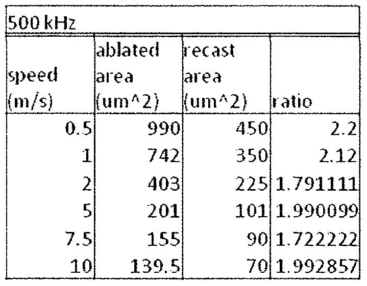
[0037] Fig 8 is a plot showing examples of ablated cross-sectional area versus re- deposited cross sectional area as a function of scan speed and repetition rate
[0038] Fig 9 is a plot of further illustrating examples of cross-sectional area versus scan speed, normalized for average power and spatial overlap of spots [0039] Figs lOA-1 and 10A-2 show example SEM cross-sections, wherein a quantity of re-deposited material is sufficiently low such that conventional ultrasonic cleaning is effective for further debris removal, the result being applicable to. for example, thm-wafer dicing and similar applications
[0040] Fig 1OB is a plot of a ratio of ablated depth to recast height corresponding to the data shown m Figs lOA-1 and IOA-2
[0041] Figs 11 A-1 1 C show example SEM cross-sections comparing results of single and double pulse processing
[0042] Figs 1 ID-I IE are plots showing the ratio of ablated depth to recast height, corresponding to the SEM images of Figs 11 A-1 1 C
[0043] Figs 12 A- 12B are SEM images showing a portion of a wafer cut (diced) using an embodiment of a pulsed laser system, and a result obtained after conventional ultrasonic cleaning
[0044] Figs 13A-1 -13A-3 are SEM images showing results obtained with various repetition rates and scan speeds using about 200 ps pulse widths
[0045] Figs 13A-4-13A-5 are plots showing weighted ablated cross-sectional area (in square microns) and a ratio of ablated depth to recast height, respectively, corresponding to the data shown in Figs 13A-1 -13A-3
[0046] Figs 14 and 14A-1 and 14A-2 schematically illustrate various examples of configurations used to test die strength of semiconductor devices, and Figs 14B and 14C are plots illustrating examples of die strength measurements obtained after processing samples with ultrashort pulses from the example experimental system illustrated in Figs 6A and όB
[0047] Figs 15A-15D show examples of SEM images, and cross sections of samples scribed and/or cut with ultrashort pulses generated with the example experimental system of Figs 6A and 6B
[0048] Figs 16A-16D show examples of SEM images illustrating femtosecond and picosecond scribing results
[0049] Fig 17 illustrates experimental test results showing die strength of silicon dies cut with 500 fs compressed pulses or 300 ps uncompressed pulses Fig 17 also includes published nanosecond laser results and mechanical test results for comparison Circles are used to show results for dies in tension, and squares are used to show results for dies in compression Average values (and error bars) corresponding to the experimental test results are offset horizontally (to the right) of the individual experimental test results with 500 fs and 300 ps pulses
[0050] These and other features will now be described with reference to the drawings summarized above The drawings and the associated descriptions are provided to illustrate embodiments and not to limit the scope of the disclosure
DETAILED DESCRIPTION OF PREFERRED EMBODIMENTS
[0051] In the following detailed description, target mateπal generally refers to material in or on at least one region of a workpiece that is to be modified by one or more laser pulses The target material may comprise multiple materials having different physical properties
[0052] In the following detailed description, repetition rate, unless otherwise stated, generally refers to a rate at which laser pulses are delivered to a target material during laser processing of the mateπal The rate may correspond to the rate at which pulses are generated by a laser source, but the rate may also be reduced relative to the source rate in embodiments where, for example, a pulse or group of pulses is gated and delivered to the target material
[0053] In the following detailed description, reference is made to limiting accumulation of unwanted mateπal within or proximate to a target mateπal, target region, or the like Unless otherwise stated, alternative language is to not to be construed as only one of the two (or more) alternatives, but may include both (or more) alternatives
[0040] As used herein the term debris is not limiting, and geneially refers to unwanted accumulation of mateπal within or proximate a localized region Debris may result from laser-material interaction and/or a heat affected zone (HAZ) Recast, slag, redeposit and other related terms are also well known in the art Typically a heat affected zone includes mateπal heated and cooled fast enough to form molten material, and the extent of the region depends, among other factors, on the pulse duration and various material parameters Short pulses, particularly ultrashort pulses, are known to localize the heat and reduce the dimension of a heat-affected zone Overview
[0054] Embodiments are generally applicable for laser processing a workpiece, and particularly for micromachining applications For example, various embodiments are applicable to cutting, dicing, scribing, and/or engraving semiconductor substrates to form features having a typical lateral dimension of about 1 micron to about 100 microns and a depth from a few microns to hundreds of microns For example, certain embodiments may be utilized for fabrication of precise trenches and grooves in a variety of materials Extremely precise trenches m silicon are required for a vaπety of microelectronic applications Several research groups have demonstrated that the best results are obtained using femtosecond laser pulses with the laser intensity just above the ablation threshold (see, e g , Barsch, Korber, Ostendorf, and Tonshoff, "Ablation and Cutting of Planar Silicon Devices using Femtosecond Laser Pulses,'" Appl Physics A 77, pp 237-244 (2003) and Ostendorf, Kuhk, and Barsch, "Processing Thin Silicon with Ultrashort-pulsed Lasers Creating an Alternative to Conventional Sawing Techniques." Proceedings of the ICALEO, Jacksonville, USA, October 2003)
[0055] Currently, the preferred method for micro-fluidic device fabrication is via lithographic processing, often involving several cycles of ultraviolet (UV) light exposures that is followed by a solvent etch Femtosecond lasers are capable of directly machining blind and through holes of modest aspect ratio (1 10-1 100, depending upon substrate material, laser parameters and hole diameter)
[0056] It is well known that ultrashort laser pulses offer important advantages relative to conventional nanosecond lasers reduced HAZ, reduced residual stress, less sensitivity to variations in material ablation thresholds Furthermore, it is well established that relatively high processing rates can be achieved by scaling laser average power (assuming fluence on the target is greater than the material ablation threshold) and using high speed multi-pass beam scanning Ultrashort laser processing is also generally recognized as a suitable approach for reduction of slag, residue, melt formations or other unwanted byproducts of laser-material interaction However, it is also well established that the use of ultrashort pulses alone cannot guarantee improved quality Many early experiments were carried out m vacuum which simplified processing Citations to various publications, patents, and published patent applications relating to material processing with ultrashort pulses, micromachining of one-or more of semiconductor, metal, or dielectric materials used in semiconductor device manufacturing, laser-material interaction mechanisms, and systems for micromachining may be found in the priority U S provisional patent applications
[0057] Embodiments disclosed herein may be utilized to form high aspect ratio features m a material, wherein a depth to width ratio is large Such features, sometimes referred to as grooves or trenches, may be formed by controllably remo\ing material from a workpiece surface The material may be removed by repeatedly scanning focused laser pulses over a target region with a mechanism to position the target material and/or the laser pulses relative to each other
[0058] Some embodiments may be utilized for laser cutting of materials, particularly semiconductor substrates Such embodiments may also include the formation of high-aspect ratio features as part of the process For example, thm wafer dicing advantageously may use clean and precise cuts to separate wafer die without damaging nearby circuitry or structures The wafer may be diced using focused laser pulses to cut through the entire wafer, perhaps changing the depthwise position of focus during cutting in some embodiments Alternatively, laser pulses may form a high aspect ratio feature, for example, a narrow and deep cut of pre-deteimmed depth A thin depthwise portion of remaining material is then separated using a non-laser method In any case, it may be advantageous for debris and contamination to be sufficiently well controlled
[0059] Figs IA- 1 C are schematic illustrations showing a portion of a process for laser-based material modification Examples of focused laser spots 1000-a, 1001 -a are shown with an overlap factor which may be a small fraction of a spot diameter in some embodiments The overlap factoi may be different than schematically shown in Fig I A For example, the overlap factor may be approximately the same from spot to spot (e g , as schematically illustrated in Fig I A) or the overlap factor may differ from spot to spot Different laser passes may utilize different overlap factors (and/or spot shapes, spot diameters, etc ) In various implementations, some adjacent spots can substantially overlap (e g , having an overlap factor that is a small fraction of a spot diameter) or some adjacent spots can be spaced apart (e g , having an oveilap factor that is approximately the same, or larger, than the spot diameter) In various embodiments, an overlap factor may be selected to provide machined features with, for example smooth straight edges, or selected to affect heat accumulation within a region In such embodiments, the overlap factor (or other parameters) can be pre-selected prior to machining, selected or adjusted dynamically during machining, or a combination of pre-selection and dynamic selection can be used Although Fig 1 A illustrates the focused laser spots 1000-a and 1001 -a as circles having the same spot diameter, the focused laser spots can have other shapes and sizes in other embodiments Many variations in spot shape, spot size, overlap factor, etc are possible
[0060] The spots may be applied to target material of a workpiece with one pass or with multiple passes, for example with a scanning mechanism (not shown) In Figs 1 A- IC, the upper illustrations schematically show the first pass of the laser pulses (Passl ), and the lower illustrations show the Nth pass of the laser pulses (Pass N) In various embodiments, any suitable number N of processing passes may be used, for example, J , 2, 5, 10, 100, 250, 700, 1000, or more passes A simplified top schematic view of a target region is shown in Fig IB, showing a region where material was removed with the circular spots 1000-a, 1001 -a The region has a lateral dimension on the order of a spot diameter, although it is generally known that with ultrashort pulses it is possible to controllably remove material over a region smaller than a spot dimension, as taught in, for example, U S Patent No 5,656,186 In the top views shown in Figs 1 A-I C, the region where material is removed is schematically shown as a rectangle, although at least the edges orthogonal to the scan direction are typically somewhat rounded, particularly with the use of focused laser beams having an elliptical or circular cross section
[0061] With various embodiments, the features may be formed with laser spots to remove a depthwise portion of the target material, for example, about 0 5 μm or a few microns in some embodiments In a single pass a relatively small depth-portion 1000-c is removed (see upper illustration in Fig 1 C) A second pass, or N passes, then remove additional depthwise portions, as schematically represented by curve 1001 -c (see lower illustration in Fig 1 C) After N passes a feature may be formed having a desired depth and/or spatial profile Alternatively, with a sufficiently large number of passes, the material may be cleanly severed (e g , cut all the wa\ through the material, sometimes called "breakthrough") In various embodiments, the number of passes N may be 1 , 2, 3, 4, 5, 10, 25, 100, 250, 500, 750, 1000, 1500, 2000, 5000, or more The number of passes may be selected based on factors including, for example, the desired depth and/or spatial profile of the feature, the mateπal(s) forming the workpiece, whether breakthrough is desired, and so forth The number of passes may be dynamically adjusted during processing
[0062] Fig IB schematically shows a simple linear/rectangular machined pattern as viewed from above the workpiece However, machined features may be circular, elliptical, interleaved, spiral or other arbitrary shapes that will be formed by programming the relative positions of the laser pulse source and target material (e g , with a scanning mechanism, as will be further illustrated below) Similarly, the focused spot distributions may be non-circular and/or may have Gaussian or non-Gaussian spot profiles Further, various shapes may be formed as a function of depth, for example tapered, stepped, and/or curved features wherein the width of the feature varies with depth in a pre-determined manner, or approximately so High aspect ratio features may be formed alone or in combination with other features, and may be connected to a region having a lower aspect feature, for example a large diameter hole Many variations are possible with the systems and methods disclosed herein
[0063] Some parameters of interest for embodiments of "trench digging" or other applications may include, for example, the shape, depth, and quality of the trench However, in many applications, redeposited material, commonly called recast or slag, may be formed at or very near the edges of the narrow trenches The quantity of redeposited material generally increases with increased machining depth
[0064] Figure I D schematically illustrates a cross-sectional view of a machined feature 1001 -c having a depth (as in Figs 1 A-I C), but having significant redeposited material 1005-a The redeposited material 1005-a may be above a surface of the workpiece and/or within the machined feature 1001 -c A baseline of the non-processed substrate is depicted as the dashed lines in Figs ID and IE The redeposited material may also accumulate within a feature or target region, for example withm a depth of several microns below the baseline (see Fig ID)
[0065] Figure IE is representative of an example result obtainable with pulsed laser embodiments, wherein, for a fixed number of passes N, accumulation of redeposited material 1005-b is reduced (compared to the result schematically shown in Fig ID) As illustrated in Fig IE, the cross sectional area of redeposited material is reduced (relative to Fig ID) and/or the type of material deposited is in the form of fine particles as opposed to molten material of a larger dimension For example, in some embodiments, such a result is obtainable by increasing the laser repetition rate and, in this example, holding other laser parameters approximately constant In various embodiments, the accumulation of the redeposited material may be reduced within the target region, proximate to the target region, or both In various embodiments, the nature of the redeposited material (e g , the size distribution of the particles) may be altered within the target region, proximate to the target region, or both Figures 1C, ID, and IE schematically illustrate the machined features 1000- c and 1001 -c as having a cross-section shaped generally as a trapezoid The trapezoidal cross-sectional shape is intended to be schematic and is not intended as a limitation on the cross-sectional shape (or any other characteristic) of features that can be machined with various embodiments of the laser-based processing systems and methods disclosed herein In other embodiments, features can be machined that do not have trapezoidal cross-sectional shapes such as, for example, triangular shapes, rectangular shapes, rounded shapes, tapered shapes converging to a minimum width much smaller than the a maximum width, or any other suitable shape Many feature shapes and sizes are possible Also, the cross-sectional size and shape of the redeposited material 1005-a, 1005-b are intended to be schematic and are not intended as a limitation on the sizes and/or shapes of possible redeposited material
[0066] By way of example, results from machining experiments on silicon substrates showed a surprising result increasing the laser repetition rate of laser pulses from about 200 kHz to about 1 MHz, while maintaining approximately constant laser pulse energy, focal spot size, and pulse duration, produced an increase in the volume of material removed relative to the amount of material redeposited The experiments were carried out using a fiber-based ultra-short chirped pulse laser system The results suggest that pulse repetition rates of several hundred kHz up to several MHz may provide a significant improvement in processing quality For example, in certain applications, additional processing steps may not be required to remove redeposited material
[0067] Obtaining both a desired feature shape and reduction in redeposited material were best achieved with ultrashort pulses, for example, pulses less than about 10 ps in width However, increased repetition rate was also beneficial with longer pulses of about 200 ps The accumulation of redeposited material was reduced relative to slower repetition rates For some applications, benefits may also be found with longer pulse widths, for example up to a few nanoseconds, or below 10 ns
[0068] Embodiments may therefore decrease the quantity of slag and/or other unwanted material (and/or change the nature of the redeposited material), while providing for a desired shape, depth, and/or width of the features By way of example, and as will be shown later, high repetition rate processing affected the nature and quantity of re-deposited material
[0069] In certain embodiments, a measure of quality may be the depth and/or volume of a machined feature relative to a peak height, average height, and/or volume of redeposited material Another example measure of quality may be the feature depth relative to the total volume of redeposited material Suitable measures of quality may be obtained with cross-sectional samples or volumetric quantification of an affected region Various tools may be used to quantify performance, for example, surface metrology tools such as white light interferometers, Atomic Force Microscopes (AFMs), or similar tools (available from, for example, Veeco Instruments Inc , Woodbury, New York) The tools may provide for improved measurement accuracy and precision, with capability for automated or semi- automated operation The commercially available tools have proven capability for measuring surface roughness of a sample and also larger volumes of mateπal, and AFMs may be used to quantify structure of the depthwise features, for example
[0070] In some applications, for example dicing and scribing, different quality measures may be provided For example, quantification of the volume of redeposited mateπal may be a useful measure, and may be combined with cut quality as an overall figure of merit Various embodiments are particularly applicable for processing operations where high efficiency is desirable, and wherein accumulation of redeposited mateπal is detrimental or otherwise undesirable
[0071] In some embodiments micromachining may include laser scribing, dicing, or similar processing of semiconductor wafers, which may be bare or patterned Scribing and dicing are two applications with a recognized need Scribing typically removes one or more layers of multiple materials supported on a silicon substrate The die of a wafer may then be separated with a mechanical dicer With decreasing of silicon substrate thickness to below 100 μm, for example 50 μm, an increased need for laser based dicing of the substrates has developed However, in some implementations, rapid laser processing speeds are required to provide justification to replace conventional mechanical dicing Moreover, in some implementations, undesirable thermal effects are to be reduced or avoided to assure reliability of subsequent packaging processes
[0072] Figs 1 G-I (not to scale) schematically illustrates an example of a patterned semiconductor wafer 120 having several die arranged in rows and columns with streets 127 therebetween In conventional systems the wafer is typically laser scribed, and cut using a dicing saw As the thickness decreases below about 100 μm. for example 50 μm or 75 μm, mechanical dicing becomes more difficult Therefore, it is desirable to use laser dicing to reduce or eliminate mechanical dicing
[0073] Fig 1 G-2 schematically illustrates an example portion 125 of the wafer 120 By way of example, dicing is to be carried out in region 127-B along the streets The region may include several materials and bare wafer portions The circuit features shown in the streets, for example high-density grid layer 129. may be utilized for electrical or other functional tests prior to dicing The regions adjacent to street 127 contain high density active circuits, interconnects which may include solder balls, or other combinations In certain advantageous implementations, the dicing or scribing is to be carried out to cleanly cut the wafer without causing damage to circuitry, without introducing significant debris or heat affected zone (HAZ), and should provide for sufficient die strength
[0074] FIG 1 G-3 schematically illustrates a cross sectional side-view 129-1 of a portion of the wafer, the fine grid area 129 of Fig 1 G-2 The grid may be covered with one or more of dielectric and metal materials
[0075] Because potential processing speed is one possible reason for use of laser technology for thin-wafer dicing, a practical system for dicing very thin wafers is to provide for removal of a relatively large amount of material at high speed
[0076] Workpiece materials in the streets may include, but are not limited to, metals, inorganic dielectrics, organic dielectrics, semiconductor materials, low-k dielectric materials, or combinations thereof The combinations of materials may be arranged in widel> varying spatial patterns and/or stacked in depth For example, microelectronic circuits may comprise portions having alternating layers of copper and low-k mateπal, covered by an overlying passivation layer Other combinations and/or configurations of mateπals are possible
[0077] Various studies disclosed results and models for micromachining of Silicon For example, Crawford et al, in "Femtosecond laser machining of grooves in Silicon with 800 nm pulses, Applied Physics A 80, 1717-1724 (2005) investigated ablation rates (in vacuum) as a function of pulse energy, translation speed, number of passes, and polarization direction (parallel vs perpendicular to translation direction, and with circular polarization) Laser parameters included 150 fs pulses at 800 nm wavelength with laser pulse repetition rate of 1 KHz Maximum translation speed was about 500 μm/sec A spot size was about 5 μm
[0078] Single and multiple pass results were reported, and motion effects analyzed A model was disclosed, including the effects of motion with high overlap between pulses assumed The approach included determining an accumulated fluence at a point along the center of a groove Despite providing a useful framework for analysis, it was recognized that the effective fluence may change somewhat for each pulse and a single or few pulse irradiation may produce much different results than many pulses, whether or not the target is moving Some conclusions reflect a little effect of translation on groove width, with the effect being difficult to quantify due to roughness and debris The results were also compared with other studies Various other morphologies were identified
[0079] Ablation performance was not predictable with a linear model over all passes Reported ablation depth per pulse well below 1 μm were generally observed with fluencies up to a few Joules/cm" Polarization effects were somewhat significant, with branching with polarization parallel to translation direction Expected ablation depth limits were observed with groove formation, apparently a result of insufficient fluence at the bottom of a groove In one example, the first few passes resulted in large amounts of material removed in a nearly linearly manner However, beyond twenty passes the amount of material ejected decreased Material re-deposition apparently competed with removal by the edges of the pulse near the nm of a groove After a large number of passes the nm was expected to largely erode away with additional passes
[0080] With our experiments increasing the repetition rate to about a few hundred KHz or greater, and preferably to at least about 1 MHz in some embodiments, improved a ratio of material removed to redeposited material compared to results obtained below a few hundred KHz The results were obtained with translation speeds suitable for high-throughput processing, and approaching some present limits of motion speed of high speed mirror systems Also, at least some results indicate too high a repetition rate will result m undesirable thermal effects, recast, and generally unwanted HAZ induced material modification Simultaneously achieving both high throughput and reduced debris is a general goal and a beneficial result that can be achieved with certain embodiments
[0081] By way of example, scribing and/or dicing of 50 μm thick or similar substrates may be carried out with a focused spot size of at least 15 μm, and with a spot size in the range of about 15-50 μm in some embodiments Other spot sizes may be used such as, for example, a few microns (e g , about 3 microns m one case) In some implementations, spot sizes in a range from about 1 micron to about 5 microns are used The quantity of material removed is generally determined by one or more factors including the scan speed, spot overlap, repetition rate (pulses per second delivered to surface), pulse energy, and spot diameter In some embodiments, sufficient overlap between adjacent spots on the surface provides for cutting or scribing a pattern of relatively uniform width In some experimental systems, relatively high pulse energy of at least a few microJoules with a spot size of about 15 μm will typically result m ablation within a region having diameter about 15-20 μm A scanning system, for example a galvanometer based mirror scanner, may provide scan speeds of up to about 10 - 20 m/sec
[0082] Material removal requirements vary, and heat accumulation within a region may be increased or decreased with suitable selection of one or more factors including pulse energy, repetition rate and speed parameters It may be desirable to increase heat accumulation within a region to facilitate material removal in some embodiments In various embodiments ultrashort pulses may be applied at a high rate and reduced motion speed to induce thermal effects similar to non-ultrashort pulses In at least one embodiment one or more of pulse energy, repetition rate, speed, and pulse width may be adjusted In some embodiments available pulse energy will be at least about 5 μj, repetition rates will be adjustable up to about 10 MHz, beam speed at the surface may be in a range of about 0 1 m/sec up to about 10 m/sec, and pulse widths provided within a range from below 1 picosecond up to a few nanoseconds By way of example, with 1 MHz rate, 40 μm spots, and speed of 0 1 m/sec, the overlap between spots exceeds 99% Localized heat accumulation may be significant If the 1 MHz rate is maintained, and speed is increased to about 5m/sec, the spot overlap decreases by 50-fold, with decreased heat accumulation within a processing region Accordingly, in various advantageous embodiments, overlap factors may be utilized that are in a range from about 0 001 to about 0 99 Other ranges are possible
[0083] Because materials within the streets may vary with different wafer designs it is desirable for some implementations of a laser system to provide for adjustment of certain parameters over a wide range For example, the scan speed, pulse energy, repetition rate (rate at which pulses impinge the surface), pulse width, and spot size are preferably adjustable over a wide range, for example at least 2 1 in some embodiments One or more such parameters, for example the pulse width, speed, and repetition rate, may be adjustable over more than a 10 1 range Other adjustable ranges are possible in other embodiments
[0084] Different laser and speed parameters may be required for scribing and bare silicon dicing, as a result of different material properties In some embodiments material removal will be facilitated with increasing heat accumulation with relatively high pulse energy and high overlap between pulses, for example greater than 99% overlap A sufficiently well controlled heat-affected zone (HAZ) is to be maintained to avoid collateral damage or increased debris in some of these embodiments
[0085] A typical multimateπal device, for example a patterned wafer, may include conductor, dielectric, and semiconductor materials stacked in depth Processing of a typical multimateπal device may be carried out at, for example, a 1 MHz repetition rate, a spot size of about 40 μm, and at motion speeds producing overlap between about 75% to more than 99% between adjacent spots
[0086] By way of example, with a pulse repetition rate in the range of about a few hundred kHz to about 10 MHz, the scan speed may be controlled in such a way that tailors the heat accumulation to facilitate material removal while simultaneously limiting debris and controlling HAZ In some implementations, removal of metal and dielectric layers may be carried out at a scan speed substantially slower than a scan speed used for removal of bare silicon As a result, the overlap between adjacent spots for removal of at least one of a metal and dielectric may be greater than an overlap for bare wafer processing (e g , at least about ten-times greater in some embodiments) A focused spot size in the range of about ] 5-40 μm, and typically about 30-40 μm, provides for high throughput in some cases [0087] Referring again to Fig 1G-2, the width of street 127 may be reduced in certain wafer designs, for example to a few ten of microns A corresponding reduction in spot size from certain preferred values above (e g about 40 μm in some cases) may be advantageous For example, a spot size of about 5 μm may be useable for cutting, scribing, or other processing operations within a street having a width of about 25 μm Some laser parameters may be scaled accordingly, and various design options may be utilized to avoid physical limitations associated with certain parameters Other spot sizes may be used such as, for example, a few microns (e g , about 3 microns in one case) In some implementations, spot sizes in a range from about 1 micron to about 5 microns are used Spot sizes of about a few microns may be advantageous for processing narrow street widths (e g , less than a few tens of microns)
[0088] Referring again to Fig 1G-2, a cutting path 127-b within street 127 is illustrated, the cutting path 127-b centered on the street region in this example It is known that wafer scribing and breaking may be carried out with a combination of a laser, for example a nanosecond pulsed laser, and a dicing saw The nanosecond laser may, in some implementations, scribe two lines at approximately equal distance from the center of the street A dicing blade centered on the street is used to cut through the remaining wafer, thereby producing individual die Embodiments descπbed herein may also be used to modify material along any path (e g , a pre-determmed path for the wafer), and/or may be used in various combinations (e g , with a dicing saw) The material to be modified or processed may comprise metal, dielectrics including low-k materials, and/or semiconductors Moreover, processing of ultra-thin wafers, such as, for example 50 μm thick wafers, can be carried out with a femtosecond laser to cut through the entire thickness of the wafer, or a substantial portion thereof, in some implementations Some embodiments may reduce or eliminate use of mechanical dicing of such ultra-thin wafers
[0089] For example, in certain implementations, requirements for precision positioning may increase, but total pulse energy may be decreased It is well known that a decreasing spot size at a particular wavelength results in a decreased depth of focus (DOF) The DOF decrease generally varies as the square of the spot size If processing over a large depth range is required various well known methods and systems for dynamic focusing, or improvements thereof, may be applied in some cases By way of example, as the spot size decreases from 50 μm to 5 μm the DOF decreases by 100-fold On other hand, the total pulse energy to achieve a given fluence over a spot area decreases as the square of the spot diameter In some implementations, much lower maximum pulse energy may be used for smaller spot sizes, and a maximum pulse energy may be, for example, about 100 nJ, or up to about 1 μ J, for processing of various dielectric, conductor, and semiconductor materials A smaller spot size may lead to some considerations for motion control also Reduced scan speeds may be utilized in some embodiments, but a requirement for precision positioning may also be increased
[0090] Therefore, in some embodiments, pulse energy and speed may be scaled downward while processing at a given fluence and repetition rate By way of example, assume pulse overlap exceeding 99% (e g at least 99 5%), a 1 MHz repetition rate, and a spot size of about 4 μm (e g approximate 10-fold reduction from the 40 μm spot size used in some embodiments) In this example, corresponding scan speed is on the order of 10 mm/sec The fluence may be obtained with pulse energy may be scaled down from a range of at least a few microjoules (e g 5 μj) to below 100 nanojoules (e g 50 nJ) as a result of a 10-fold decreased spot size
[0091] Similarly, in some embodiments, the repetition rate may be increased to tens of MHz, and with relatively low pulse energy for certain micromachining operations For example, some cutting or scribing applications may require selective removal of a single layer of material, or a few layers, with relatively low fluence
[0092] Referring to Fig 1 G-3, one of more layers are schematically represented by shaded regions (not necessarily to scale), and may comprise dielectric and/or metal materials The underlying bare wafer (not shaded) is processed by the laser after modification of the overlying layers in certain processing applications The inventors also discovered that thermal processing (e g , heat accumulation) and/or a sufficient heat affected zone (HAZ) reduces or avoids delammation and/or cracking of composite layers or certain mateπal (e g low-k dielectrics) Also, reduced HAZ associated with ultrashort pulses may be beneficial for cutting through the wafer for singulation of die By way of example, if nanosecond pulses are used both to remove layers and for dicing the silicon wafer performance may be insufficient or unpredictable For example, it is known that weak die strength and various other material issues are caused by excessive HAZ caused by nanosecond pulses [0093] Without subscribing to any particular theory, when a wafer is irradiated with a laser pulse, electrons m the wafer absorb energy from the laser beam almost immediately As a result of collisions between hot electrons and the lattice, thermal equilibrium between the electron system and the lattice is quickly achieved, and the exposed area increases in temperature The time to reach the equilibrium vanes as a function of material, and may be hundreds of femtoseconds to tens of picoseconds Thermal energy within the exposed region will transfer to its surrounding cooler area The rate of cooling is affected by several parameters, for example material, temperature differential between the hotter and cooler area, as well as the temperature distribution As an example point of reference, an approximate period, when silicon stays above its melting temperature, is about hundreds of ps
[0094] When a nanosecond (or longer pulse duration) laser is used for dicing or scribing process, the irradiated region remains above its melting temperature for an extended time frame A "melting pool" (e g a region of molten material) will be formed and will shrink when it is cooling down The "boiling"' and "cooling" process causes cracking, surface roughness and voids m the HAZ Such a process can be erratic, and the quality of material modification difficult to predict
[0095] Femtosecond pulse irradiation in some implementations provides a shallow HAZ, but little interaction with underlying layers of a device occurs as a result of the ultrashort pulse width The femtosecond heating process is almost instantaneous, confines HAZ to a limited thickness, and does not substantially affect layers disposed below modified material Much smoother and predictable surface morphology is achievable in certain such implementations
[0096] However, as a result of the very shallow HAZ formed by an ultrashort laser pulses m some of these implementations, little or no material modification of multiple materials occurs For example, melting between layers may be absent Thus, dicing or scnbing performance with multilayer devices, specifically devices having at least one low-k material, can be somewhat limited using femtosecond laser pulses in these implementations Moreover, delammation may occur in some of these implementations However, the inventors discovered, as will be shown in experiments described below, that in some embodiments of the systems and methods described herein, increasing pulse energy and/or fluence, and/or decreasing scan speed, provided good processing results in multi-material target regions Accordingly, the inventors' results described herein may be used to control heat accumulation and/or HAZ within one or more materials of the target For example, embodiments of the systems and methods disclosed herein may be configured to provide sufficiently high heat accumulation in a target to reduce or avoid delammation (e g , delammation of a dielectric material and a metal material)
[0097] In some embodiments multiple lasers may be utilized, and configured m an integrated laser system having multiple sources, or as a source having adjustable pulse widths By way of example, a relatively long pulse width, for example hundreds of picoseconds and up to a few nanoseconds, may be utilized to increase HAZ for processing a first depthwise portion of a workpiece, and particularly for removing low-k layers and/or other metals and/or other dielectrics Such metals may include, but are not limited to, copper, aluminum, and/or gold Dielectric materials may include, but are not limited to, silicon dioxide, silicon nitride, and/or various organic or inorganic materials The arrangement of the dielectric and/or metal materials may vary in three-dimensions as schematically illustrated in the examples shown m Figs 1 G-I to ϊ G-3
[0098] In some embodiments, ultrashort pulses may be used to process a second depthwise portion of the workpiece, with generation of negligible HAZ In various embodiments femtosecond pulses are utilized for at least cutting through the entire wafer, or a substantial fraction of the wafer, and particularly for cutting very thin wafers, for example wafers having thickness of 100 μm or less Moreover, in some of these embodiments, at least a portion of the processing of metals and/or dielectrics may also be earned out with femtosecond pulses
[0099] In at least one embodiment a single laser source may be utilized Adjustment of laser parameters may balance heat generation within a processing region and transfer of heat outward from the region Delammation and/or unwanted thermal stress are then reduced or avoided
[0100] In various embodiments a picosecond pulse width may be utilized to remove a low-k material For example, at least one pulse may be in the range of about 100 ps to about 500 ps, about 100 ps to 250 ps, or in the range of about 200 ps to 500 ps In some embodiments at least one pulse may have a pulse energy may in the range of about 2 μj to 10 μj over a spot diameter of 30-40 μm, corresponding to a fluence at least about 0.15 J/cm2, for example. Such examples of pulse widths and fluence can generate sufficient HAZ for processing metal and dielectrics, and within a period of time to provide material modification, (e.g.: melting and removal) of multiple layers. However, any region of melted material is also sufficiently shallow (e.g.: not too deep) so that unwanted cracking, surface roughness and/or voids in the HAZ are reduced or avoided. In other embodiments, other pulse widths, pulse energies, spot diameters, and fluences may be used.
[0101] In some device designs the width of street 127 may be reduced. Embodiments of the laser system may then be configured with a reduced spot size for processing in a narrowed region. In some of these embodiments, the pulse energy can then be reduced while maintaining a given fluence. However, in some applications a relatively high fluence may be selected for processing and may be advantageous for processing of various metals and dielectrics.
Example Embodiments of Pulsed Laser Systems for Micromachining
[0102] Fig. IF schematically illustrates an embodiment of a system 100 suitable for processing a workpiece with laser pulses. The system 100 comprises a laser system 104 that is operatively coupled to a controller 1 14 and scanning system 106. In some embodiments, the laser system 104 is configured to output laser pulses that comprise one or more ultrashort pulses (USP). For example, in at least one embodiment, the laser system 104 comprises a USP laser. In various embodiments the system 100 will provide for adjustment of certain pulse parameters over a substantial range. Such parameters may include one or more of pulse energy, pulse repetition rate, pulse width, spot diameter, overlap of adjacent spots, and scan speed. By way of example, pulses may be generated at an adjustable repetition rate up to about 1 MHz, or up to about 10 MHz. An output pulse may have an energy of about 1 μJ or higher, for example up to about 5-20 μj, and a pulse width about 1 ps or shorter. Further details of various embodiments of the system 100 are described below.
[0103] An amplified laser system, particularly an ultrashort fiber-based chirped pulse amplification system (FCPA), operating at repetition rates of at least several hundred kHz, is suitable for processing of several types of patterned and unpatterned substrates. High pulse energy, for example several microjoules, is obtainable with an amplified train of ultrashort pulses Sufficient pulse energy in at least the microjoule range is obtainable, with 15-40 μm typical spot diameters providing for high throughput in some embodiments
[0104] In some implementations, multiple passes can be used The pulse energy used in the passes may be the same or different than the energy used m additional passes Moreover, in some embodiments, the pulse energy may be varied between passes
[0105] In some embodiments other laser pulse parameters may be adjusted between passes For example, a relatively long pulse width may be used for removal of at least conductive and/or dielectric mateπals Such a pulse width may be up to a few nanoseconds (ns), less than 1 ns, or about 500 ps or shorter An ultrashort pulse may be used to cut at least the underlying silicon material, for example with sub-picosecond pulses
[0106] In some implementations, the long and short pulses may be applied in separate passes, or in some embodiments by applying bursts of laser light to a target area of a material during any single pass In some cases, the burst may be applied at a predetermined repetition rate, and may comprise at least first and second pulses of laser light displaced or overlapped in time, and the first pulse width may be greater than the second pulse width, and greater than l Ops in duration in some embodiments, the second pulse width being an ultrashort pulse, for example a sub-picosecond pulse The pulse separation of pulses in the burst may be about 1 μsec to 0 1 μsec. and in some embodiments a shorter separation may be used The second pulse width may be as above sub-picosecond (e g > 100 fs) to about 10 ps. and generally less than about 50 ps Moreover, first and second is not restricted to temporal sequence, but may be applied in any order For example a reversed order may result from respective top-side or bottom-side initial scans
[0107] One possible preferred laser system for some micromachining implementations will provide pulse energy of at least about 5 μj at an adjustable repetition rate (pulses delivered to the surface) of about a few hundred kHz to 10 MHz, and will be coupled to a scanner for scanning at a rate up to about 10 m/sec The system can include an optical power amplifier to provide for high pulse energy and sufficiently high throughput Preferably at least a portion of the system will be fiber based
[0108] In one preferred embodiment, the laser source comprises a Yb-doped, amplified fiber laser (e g , FCPA μJewel, available from IMRA America) Such a laser offers several primary advantages over commercial solid-state laser systems For example, this laser source provides a variable repetition rate over a range of about 100 kHz to 5 MHz Higher pulse energy than oscillator-only systems allows greater flexibility in focal geometry (e g larger spot sizes for a given fluence) In at least one embodiment, pulse energy of up to about 10 μj may be applied at a repetition rate of about 1 MHz, with at least about 1 μj at a 5 MHz rate Higher repetition rate than various solid-state regeneratively amplified systems allow greater speed Although some oscillators have been demonstrated which produce microjoule pulse energy, the complexity is at least comparable to CPA systems
[0109] Such energy is also achievable with embodiments of a fiber-based system utilizing a power amplifier, for example at least one large mode amplifier producing a nearly diffraction limited output beam In at least one embodiment, a large mode amplifier may receive low-energy pulses from a mode locked fiber oscillator, and amplify the pulses to the microjoule level Preferably, the oscillator and power amplifier are integrated to form an all- fiber system Numerous possibilities exist
[0110] In some embodiments, particularly for processing with lower pulse energy and/or higher repetition rates, an all-fiber ultrashort pulsed laser system may be utilized The system may include a fiber-based pulse amplification system producing pulse widths below 1 ps Low energy pulses from a fiber oscillator may be selected with an optical switch, and amplified with a fiber amplifier to at least about 100 nJ At relatively low energy the sub- picosecond pulses may be amplified with the fiber amplifier In other embodiments an all- fiber chirped pulse amplification system ma> comprise a pulse stretcher and pulse compressor The compressor may compπse a fiber compressor performing at least partial pulse compression, a bulk compressor, or a combination thereof Many variations are possible, including further amplification, harmonic conversion, and the like
[0111] Various embodiments include fiber-based chirped pulse amplification systems suitable for numerous micromachining applications The systems are particularly suited for processing materials using pulse energies up to tens of microjoules and up to a maximum of about 100 μ J Spot diameters may be in a range from about 1 micron to about 100 μm In some embodiments, a spot size may be in the range of about 10 μm to 100 μm, or 10 μm to about 60 μm, or 25 μm to 50 μm Pulse widths may be in a range from tens of femtoseconds (e g , 50 fs) to about 500 picoseconds The parameters generally provide for energy density near or above an ablation threshold for the workpiece mateπal(s) being processed, and the total energy required may depend on, for example, the spot diameter Workpiece materials may include, but are not limited to, metals, inorganic dielectrics, organic dielectrics, semiconductor materials, low-k dielectric materials, or combinations thereof
[0112] Fig IF schematically illustrates a first embodiment of a system 100 capable of use for processing a workpiece, for example a semiconductor substrate The system 100 comprises a laser system 104 and a scanning system 106 In this embodiment, the scanning system 106 includes two beam deflectors 108, for example galvanometπc scanning mirrors, capable of two-dimensional scanning In other embodiments, a different number and/or type of scanning mirrors may be used In some embodiments, the scanning may be one-dimensional The scanning system 106 may also include focusing optics 110 such as, for example, an integrated F-theta lens capable of producing a substantially flat field of view at the target substrate 1 12 For example, in some embodiments, the F-theta lens is configured to produce a 20 μm laser focus spot with a substantially flat field of view over an area of about 8000 mm' In other embodiments, for example for application to wafer cutting or dicing, a 10-50 μm laser focus spot with a substantially flat field of view over an area of about 60 mm x 60 mm may be utilized The scanning system 106 (and/or other system components) may be controlled by a controller 1 14 For example, the controller 1 14 may include one or more general and/or special purpose computers, which may be remote and/or local to the system 100
[0113] In other embodiments, additional optical elements may be utilized in the scanning system 106 (e g , mirrors, lenses, gratings, spatial light modulators, etc ) A skilled artisan will recognize that a pattern to be formed within the substrate may be communicated to the system 100 via many methods including wired and/or wireless techniques In certain embodiments, the pattern is represented via vector graphics including curves and/or polygons and may include three-dimensional machining instructions Many variations are possible
[0114] In some embodiments, the laser system 104 may comprise a USP laser configured to output one or more ultrashort pulses (USP) An ultrashort pulse may have a duiation such as, for example, less than approximately 10 ps In the example system 100 shown in Fig I F the laser system 104 may comprise a fiber-based laser capable of generating an ultrafast pulse train For example, the laser may comprise an FCPA μJewel laser available from IMRA America, Inc (Ann Arbor, Michigan) The laser pulses have a wavelength that may be about 1 μm In some embodiments, shorter wavelengths laser pulses are used such as. for example, green light pulses of about 520 nm wavelength In other embodiments, any other suitable laser system can be implemented In certain embodiments, the laser system 104 may produce laser pulses with a pulse width less than about 10 ps For example, the pulse width may be in a range from about 100 fs to about 1 ps In some embodiments, the pulse width is in a range from about 10 fs to about 500 ps In other embodiments of the laser system 104, other pulse widths are used such as, for example, < 10 ns, < 1 ns, < 100 ps, < 1 ps, and/or < 100 fs
[0115] In certain embodiments, the laser system 104 may comprise a diode-based and/or microchip laser seed source and may output pulses having durations of about a nanosecond, a few nanoseconds, and/or up to about 10 nanoseconds The laser system 104 may comprise any suitable type of laser for outputtmg pulses having desired properties
[0116] In some embodiments, a relatively high laser repetition rate is used to enable relatively rapid laser processing For example, the repetition rate may be larger than 500 kHz In certain embodiments, a repetition rate of about 1 MHz to \ 0 MHz may be used Other repetition rates are possible Based on results disclosed herein, the use of a relatively high repetition rate may be utilized in some embodiments to reduce the quantity of redeposited material 1005-a schematically illustrated in Figure ID In some implementations, tens or hundreds of laser pulses may overlap in each focal spot diameter, which may be about 20 μm m diameter, or 10-50 μm in some embodiments In other embodiments a different numbei of pulses may overlap For example, in some embodiments a few pulses may overlap, for example 3 pulses Another possible advantage of a relatively high repetition rate is the ability to process the substrate in a shorter time than when a lower repetition rate is used As such, in certain embodiments, the throughput of the system 100 is improved while simultaneously piovidmg improved quality
[0117] Fig 2 A schematically illustrates an embodiment of a system 200 that can be used for processing a semiconductor a target substrate 1 12 via with ultrafast pulse trains This system 200 may be generally similar to the embodiment schematically depicted in Fig I F The laser system 104 in the embodiment shown m Fig 2A comprises an optional internal pulse modulator 202 not shown in the embodiment depicted m Fig IF The optical modulator 202 may be used for modulation of the repetition rate of the laser pulse train In some embodiments, the laser pulse train comprises one or more ultrashort pulses such as, for example, one or more trains of ultrashort pulses In some embodiments, the modulator 202 is adapted to change the laser pulse repetition rate from the oscillator repetition rate (typically about 50 MHz in some fiber laser embodiments) to the machining repetition rate (typically less than or about 1 MHz) For example, the modulator 202 may be configured to allow for transmission of only every nth pulse from the oscillator pulse train to a final power amplifier, or transmission of groups of pulses In certain embodiments, it may be convenient to implement such oscillator amplifier configurations for the generation of high energy pulse trains, where for improved oscillator stability, oscillator repetition rates of the order of 50 MHz are utilized Such oscillator amplifier systems are well known to a skilled artisan
|0118] In certain implementations, the internal modulator 202 allows the average power and thermal conditions in the amplifier to remain substantially the same while substantially instantaneously changing the pulse energy and pulse peak power The internal modulator 202 may comprise an acousto-optic modulator or any other suitable optical modulator In certain embodiments, the laser system 104 outputs pulses with pulse energies above about 1 μJ, pulse durations less than about 10 ps, and a pulse repetition rate of greater than about 100 kHz
|0119] The embodiment shown in Fig 2A also comprises a frequency converter 204 such as. for example, a second harmonic generation (SHG) converter In this embodiment, combination of the SHG converter and the internal modulator 202 provides a "fast shutter," because the harmonic conversion efficiency is proportional to the laser pulse energy Accordingly, by modulating the laser repetition rate from the oscillator it is possible to tuin the machining beam (e g , the transmitted SHG beam) on and off substantially instantaneously Such rapid shuttering is not possible mechanically and is difficult to implement optically for high laser powers without causing degradation to beam quality, pulse duration, etc Some embodiments may include a third harmonic generation converter and/or a fourth harmonic generation converter or any other suitable harmonic generation converter
[0120] The embodiment shown in Fig 2A also comprises the controller 1 14, which may be used to control the laser system 104, the scanning system 106, the frequency converter 204, and/or other system components For example, in certain embodiments, control of the modulator 202 and the scanning system 106 (e g , the scanning mirrors 108 and/or the focusing optics 1 10) may be linked so as to enable much greater control of the laser irradiation conditions, thereby providing greater control of machining depth and lateral extent For example, m some embodiments, the controller 114 is configured to control a spatial overlap between adjacent focused pulses (or groups of pulses) during processing of a target material at the pulse repetition rate
[0121] Fig 2B schematically illustrates an embodiment of a system 230 capable of use for processing target substrates with ultrafast pulse trains In this embodiment, the laser system 104 includes a chirped pulse amplification system such as, for example, a fiber- based chirped pulse amplification (FCPA) system Advantages of using an FCPA system include improved efficiency and reliability Also, since the output energy and peak-power of a fiber amplifier generally decrease as the repetition rate of the oscillator increases, with substantially constant average output power or with fixed pump power The fiber amplifier output energy and power variation as a function of repetition rate may be exploited to provide improved FCPA performance
[0122] Various U S patents assigned to the assignee of the present application disclose chirped pulse amplification systems using compact fiber configurations The disclosure of each of the following U S patents is hereby incorporated by reference herein m its entirety U S Patent No 5,499,134, issued March 12, 1996 to Galvanauskas, et al , entitled "Optical Pulse Amplification Using Chirped Bragg Gratings," U S Patent No 5,696,782. issued December 9, 1997 to Harter, et al , entitled "High Power Fiber Chirped Pulse Amplification Systems Based On Cladding Pumped Rare-Earth Doped Fibers," and U S Patent No 7,1 13,327, issued September 26, 2006 to Gu, et al , entitled "High Power Fiber Chirped Pulse Amplification System Utilizing Telecom-Type Components" (hereinafter referred to as "the '327 patent") Any of the laser systems disclosed in these patents, as well as other commercially-available "all fiber" laser systems, may be used with the system 230 shown in Fig 2B
[0123] In certain embodiments, the laser system 104 comprises an FCPA μ Jewel laser (available from IMRA America, Inc , the assignee of the present application), which provides laser pulses at an output of a compressor 252 The output pulses may be generated at an adjustable repetition rate up to about 1 MHz An output pulse may have an energy of about 1 μj or higher, and a pulse width about 1 ps or shorter In some embodiments, if the peak power and pulse energy are low enough to avoid non-linear effects, a fiber compressor, rather than a bulk output compressor, may be used for pulse compression In certain embodiments, photonic bandgap fibers or photonic crystal fibers may be used alone or in combination with bulk compressors or large area fibers to provide for increased output energy and peak power
[0124] In the embodiment of the system 230 schematically illustrated in Figure 2B, the laser system 104 comprises a single-pass fiber-based chirped pulse amplification system The laser system 104 includes a high repetition rate source 232, a fiber stretcher 236, a fiber pre-amphfϊer 240 a pulse selector/modulator 244. a fiber power amplifier 248, and a compressor 252 The output of the compressor 252 may be an ultrashort pulse tram In some embodiments, the compressor 252 may be detuned to provide longer pulse widths (e g , about 200 ps) In other embodiments, the compressor 252 is not used, and the laser system 104 outputs pulses having widths up to about a nanosecond, a few nanoseconds, and/or up to about 10 nanoseconds In some embodiments, the laser system 104 may include one of more of a single-pass and double-pass pre-amphfier, a single or double-pass stretcher, and power- amplifier arrangement (not shown), which may provide longer stretched pulse widths and higher pulse energy in a comparable package size Some embodiments may comprise polarization maintaining (PM) fiber amplifiers, oscillators, and stretcher fibers As described above, the controller 1 14 may be configured to coordinate delivery of the pulses to the target substrate 1 12 via the scanning system 106 In various embodiments, the controller J 14 may be used to control some or all of the components of the laser system 104, the scanning system 106, and/or other system components In one embodiment, the controller 1 14 is configured to control the laser system 104 by controlling the pulse selector/modulator 244 As descπbed above, the scanning system 106 may include, for example, a scanning mirror 108 such as, e g , a galvanometer scanning mirror The scanning system ] 06 may also include focusing optics 1 10
[0125] The high repetition rate source 232 may provide a free-running pulse tram operating at a repetition rate well above 1 MHz, for example, in a range of about 20 MHz to about 100 MHz Mode-locked lasers, including all-fiber-based passive mode-locked or other devices, may be used to produce such repetition rates Corresponding pulse widths may be in a range from about several hundred femtoseconds to about 10 picoseconds, for example In other embodiments, non-mode locked laser sources may be used For example, output of a quasi-cw semiconductor laser may be modulated and optionally compressed to produce picosecond or femtosecond pulses Suitable laser sources include the sources described in U S Patent Application No 10/437,057 to Harter, entitled "Inexpensive Variable Rep-Rate Source For High-Energy, Ultrafast Lasers." now U S Patent Application Publication 2004/0240037, assigned to the assignee of the present application, and hereby incorporated by reference herein in its entirety
[0126] The fiber stretcher 236 may include a length of optical fiber (e g , about 100 m to 1 km depending on fiber dispersion) to stretch pulses from the high repetition rate source 232 in order to avoid non-hnear effects and/or damage to the fiber pre-amplifier 240 and/or the fiber power amplifier 248 The stretcher 236 may comprise a fiber Bragg grating (FBG), a chirped FBG, or a combination thereof The stretcher 236 may comprise fiber having anomalous third order dispersion (TOD). so as to partially compensate residual TOD (if present) that may be accumulated in the system In some embodiments, the majority of residual TOD results from the use of mismatched stretcher (fiber-based) and compressor dispersion (bulk-gratmg based) In various example embodiments, the width of a stretched pulse may be about 50 ps, in a range from about 100 ps to about 500 ps, or in a range up to about 1 ns Pulse stretching may also be provided in double pass arrangements
[0127] The fiber pre-amplifier 240. which is optional in some laser systems 104, amplifies the energy of a pulse emitted from the high repetition rate source 232 The source 232 may emit pulses with energies from about several hundred pj to about 1 nJ and up to about 5 nJ In some embodiments, the pulse energy at the output of the pre-amplifier 240 may be above about 1 nJ, for example, in a range from about 1 nJ to about 20 nJ, and m some embodiments up to about 100 nJ In some embodiments a large-mode amplifier may be used as a pre-amphfiei so as to produce microjoule seed pulses For example, various amplifier options developed by the assignee of the present application (e g amplifiers utilizing a multimode fibei, large core leakage channel fiber, photonic crystal fiber, and/or photonic bandgap fiber) that provide a high quality output beam are further described below and useable as either pre-amphfϊers, power amplifiers, or generally as at least a portion of a multistage amplifier
[0128] The pulse selector/modulator 244 may be configured to selectively transmit pulses to the power amplifier 248 The pulse selector/modulator 244 may include an acoustic-optic modulator (AOM), an electro-optic modulator (EOM), a high speed Mach- Zehnder device (MZ), and/or an electro-absorption modulator (EAM) AOMs do not require high voltage electronics, and commercially available digital driver electronics provide ease of use Mach-Zehnder modulators (MZs) are integrated optical devices having GHz bandwidths and low drive voltages, and in many cases, require a polarized input beam In some embodiments, the relatively small area of an integrated MZ device may limit useable peak- power In some embodiments, the pulse stretcher 236 reduces peak power incident on the modulator 244, as described in the '327 patent MZ devices have been used at 1 55 μm telecom wavelengths and MZ devices are now available at 1 μm wavelengths The '327 patent discloses a chirped pulse amplification system using MZ modulators In certain embodiments, the pulse selector/modulator 244 may provide for about 20 dB to about 30 dB of intensity control, and may be useable to at least partially control output intensity based on the transfer characteristic of the power amplifier 248 as a function of input
[0129] In certain embodiments, the fiber power amplifier 248 comprises a multimode fiber amplifier configured to provide an output substantially in the fundamental mode For example, the system may utilize a fiber power amplifier as described in U S Patent No 5,818,630, issued to Fermann, et al , entitled "Single-Mode Amplifiers and Compressors Based on Multi-Mode Fibers," assigned to the assignee of the present application, and hereby incorporated by reference herein in its entirety Multimode fiber amplifiers provide production of peak powers and pulse energies that are higher than those achievable in single-mode (SM) fibers before the onset of undesirable nonlineaπties and gam saturation In other embodiments, large-area amplifiers may be utilized, for example photonic bandgap or photonic crystal designs High quality output beams were demonstrated with leakage mode designs, for example, as described in U S Patent Application No 1 1/ 134,856, entitled, "Single Mode Propagation in Fibers and Rods with Large Leakage Channels," published as U S Patent Application Publication 2006/0263024, assigned to the assignee of the present application, and hereby incorporated by reference herein in its entirety
[0130] As descπbed above, the compressor 252 is an all-fiber compressor in some embodiments However, if peak power is too high, for example about 100 kW or greater m some implementations, non-hnear effects may limit performance of an all-fiber compressor A tradeoff may then exist between the compactness of a fiber design and the flexibility associated with a bulk compressor In some embodiments, both fiber and bulk components may be used in the laser system 104
[0131] The high repetition rate source 232 may produce pulses having an output wavelength of about 1 μra In some embodiments, the system 230 comprises an optional frequency converter 256 For example, the frequency converter 256 may comprise a frequency doubler, a frequency tπpler, and/or a frequency quadrupler producing respective visible (e g , green) or ultraviolet output wavelengths (for 1 μm input wavelengths) In some embodiments the frequency converter 256 may comprise a parametric amplifier Conversion efficiency is generally improved with higher peak intensity Therefore, the frequency converter 256 advantageously may be positioned to receive the output of the compressor 252 In one example embodiment, the frequency converter 256 was configured to provide second, third, and fourth harmonic generation Second harmonic generation was accomplished using a type I non-cπtically phase-matched lithium tπborate (LBO) crystal The third harmonic was produced by sum frequency mixing the fundamental and the second harmonic m a type II critically phase-matched LBO crystal A type I LBO and type I beta barium borate (BBO) crystal can also be used in embodiments for 3rd harmonic generation, producing near UV output wavelengths A type I critically phase-matched beta baπum boiate (BBO) crystal generated the fourth harmonic by frequency doubling the second harmonic light In this example embodiment, light having 50 μJ, 500 fs pulses at a fundamental wavelength of 1040 nm was input to the frequency converter 256, which provided 53%, 25%, and 10% conversion efficiency to second, third, and fourth harmonic frequencies, respectively At a laser repetition rate of 100 kHz, this example embodiment produced an average power of about 5 00 W at 1040 nm and average converted powers of about 2 62 W at 520 nm, about 1 20 W at 346 nm, and about 504 mW at 260 nm The converted pulse energies were about 26 μJ at 520 nm, about 12 μJ at 346 nm, and about 5 μJ at 260 nm Further details of a laser system 104 that may be used for providing frequency converted ultrashort pulses are described in "12 μJ, 1 2 W Femtosecond Pulse Generation at 346 nm from a Frequency- tripled Yb Cubicon Fiber Amplifier," by Shah, et al , 2005, CLEO 2005 Postdeadhne, CPDBl, which is hereby incorporated by reference herein m its entirety
[0132] The controller 1 14 may be used to coordinates the positioning of the scanning beam and the selection of laser pulses In certain embodiments, when the high repetition rate source 232 is free-running, a portion of the beam is detected using a length of optical fiber coupled to a high speed photodetector (not shown) The photodetector output provides a synchronization signal to the controller 1 14 The synchronization signal advantageously may be a digital signal The scanning system 106 may include 2-D galvanometer mirrors 108 such as, for example, hurrySCAN® II 14 scan heads available from SCANLAB America, Inc (Naperville. Illinois) Advantages of using such scan heads include that they are low inertia-devices and are provided with user-friendly commercially available controllers so that mirror position and/or velocity signals are readily programmable The scanning system 106 and the controller 1 14 may also be used with any suitable combination of translation stages rotation stages, and robotic arm (not shown) to position the target substrate 112 In some embodiments the scanning mirrors 108 may be omitted and any other suitable system for relatively moving the laser beam and the target substrate 1 12 Suitable focusing optics 1 10 such as, for example, an F-theta lens and/or a high resolution objective may be used to focus each laser pulse onto the surface of or in the target material Some refractive optical elements may introduce spot placement and focusing errors, or other temporal or spatial distortions, resulting from material dispersion In certain embodiments, commercially available optic elements designed for ultrashort laser pulse beams are used In certain embodiments, the controller 1 14 is configured to control spatial overlap between adiacent focused laser pulses (or groups of laser pulses) during processing of the target material
[0133] In certain embodiments it may be desirable to operate the amphfier(s) substantially continuously to reduce the likelihood of damage and to provide for maximum energy extraction from the amplifiers Fiber amplifiers are well suited for amplifying high speed pulse trains However, in some embodiments, increased risk of amplifier damage occurs and undesirable amplified spontaneous emission (ASE) is generated during extended periods where material processing does not occur ("idle periods") For example, in some amplifiers, the idle time period may be in a range from tens of microseconds to hundreds of milliseconds or greater In certain fiber amplifiers, an idle time of about 100 μs may be sufficient for gain to increase to a sufficient level for free-lasmg under high gam (strong pumping) conditions After about 25-40 μs of idle time, if a seed pulse is injected, the built up gam in the amplifier may have sufficient gam to create a high energy pulse capable of inducing damage to the output fiber facet Accordingly, in certain embodiments, stabilization and protection of the laser components is provided by dynamic adjustment of the input pulse energy and/or control of a pump diode current as descπbed, for example, m U S Patent Application No 10/813,173, to Nati, et al , entitled "Method And Apparatus For Controlling And Protecting Pulsed High Power Fiber Amplifier Systems," published as U S Patent Application Publication No 2005/0225846, assigned to the assignee of the present application, and hereby incorporated by reference herein in its entirety
[0134] In various embodiments of the system 230, the controller 1 14 can be configured to operate the pulse selector/modulator 244 at a high repetition rate (e g , from about 50 IVIHz to about 100 MHz) during idle periods During idle peπods, the amplifier 248 is generally operating m a non-saturated regime The power amplifier average output may slightly increase at the fundamental wavelength Modulation of the pulse energy between an idle period and an "active'" period (when the system 230 is processing the target) may be sufficient to provide rapid shuttering of the beam (e g , "off and "on" functionality) In some implementations, the laser fluence on the target substrate 1 12 during some "idle" peπods may be above the ablation and/or surface modification thresholds, but the modulation in fluence between "idle" and "active" peπods may be sufficient for process control In some embodiments, an optional shutter 260 may be used to control the energy incident on the target substrate 1 12 The optional shutter 260 may comprise an acousto-optic device, an opto-mechamcal shutter, and/or an electro-optic shutter
[0135] Certain embodiments of the system 230 include a frequency converter 256 that may provide, for example, frequency doubling and/or tripling hi certain such embodiments, the pulse energy and/or the peak power may be relatively low at the output of the frequency converter 256 In such cases, output of the converter 256 may be a relatively low energy pulse with most energy content at the fundamental wavelength and, at focus on the target, the energy may be below the ablation and/or surface modification thresholds of the target material In some system embodiments, modulator adjustment of about 20 dB to about 30 dB may provide control of intensity over a wide operating range so as to avoid altering target material properties
[0136] In certain embodiments, techniques may be used to attenuate unwanted beam energy For example, unwanted energy may be removed with a spectral filter (not shown) In some implementations, polarization filtering may be possible, because of the difference in polarization state between fundamental and harmonic frequencies for Type I phase matching The pulse selector/modulator 244 also may be controlled to limit the energy to the amplifier 248 Focusing optics in the scanning system 106 (or other focusing optics if a scanner is not used) may be optimized for the machining wavelength (which may be a frequency converted wavelength if the optional frequency converter 256 is used) In some implementations, the focusing optics may be configured so that the spot size of the fundamental wavelength is increased so that the energy density at the surface of the target substrate 1 12 is reduced
[0137] During active processing periods, the controller J 14 may be used to provide signals to the pulse selector/modulator 244 to "down count" or otherwise select pulses In some embodiments, processing repetition rates may be from about 100 KHz to about 10 MHz During active processing, it may be advantageous for the laser to operate in saturation, or approximately so, in order to extract the maximum energy from the fiber amplifier
[0138] Fig 3 schematically illustrates an embodiment of a system 300 capable of use for machining a workpiece (or target substrate) 1 12 via ultrafast pulse trains This system 300 may be generally similar to the embodiments depicted in Figs IF and 2A, 2B The system 300 may further comprise a robotic arm system 304 coupled to the target substrate 1 12 and configured to manipulate the target position (and/or orientation) relative to the scanning beam The robotic arm system 304 may be a single-axis or a multi-axis system In some embodiments, the scanning system 106 comprises a scan head that is moved with respect to the target substrate 112 A possible advantage of embodiments providing relative movement between the scan beam and the target substrate 1 12 is that the system may enable processing of non-flat surfaces [0139] In some embodiments of the systems 100, 200, 230, and 300 schematically shown in Figs 1 -F, 2A, 2B and 3, respectively, the laser spot size is primarily determined by the F-theta lens in the scanning system 106 In some implementations, in order to have reasonable processing area for images, spot sizes larger than about 10 μm are used Certain embodiments of the laser system 104 are capable of machining much smaller spot sizes (e g , < 1 μm) For such small focal dimensions, significantly lower pulse energy is used m some embodiments In order to achieve sufficiently high resolution over a sufficiently large working area, the target and the beam may be moved with respect to each other For example, the target may be moved relative to a substantially stationary laser beam (or vice- versa)
[0140] In certain embodiments of the systems 100, 200, 230, and 300, a variable telescope can be positioned along an optical path between the laser system 104 and the scanning system 106 In certain such embodiments, the F-theta lens may be omitted from the scanning system 106 The variable telescope may be used to dynamically vary the focal length of the system and may provide continuous variation of the focal spot size on the target substrate 1 12 A commercially available variable telescope system may include, for example, the vaπoSCAN dynamic focusing unit available from SCANLAB America, Inc (Naperville, Illinois) Such a system, with dynamic focusing, provides capability for 3D adjustment of the beam focal position, and useful capability for following or compensating variations in the target surface locations, as might be caused by substrate warpage or other deviations from flatness
[0141] Fig 4A schematically illustrates an embodiment of a system 400 capable of use for processing semiconductoi substrates with ultrafast pulse trains This embodiment comprises a laser system 104 and a translation stage 408 configured to move the target substrate 1 12 relative to the laser beam In certain embodiments, the translation stage 408 remains in substantially constant motion with relatively high translation speeds in order to enable sufficiently high processing speeds In some embodiments, the translation stage 408 may include an X-Y or an X-Y-Z translation stage For example, the translation stage 408 may include a Nano-Translation (ANTTM) stage available from Aerotech, Inc (Pittsburgh, Pennsylvania) Many techniques for relatively controlling positioning of a pulsed laser beam and a target substrate are known such as, for example, as described in U S Patent No 6,172,325 to Baird, et al , entitled "Laser Processing Power Output Stabilization Apparatus and Method Employing Processing Position Feedback " In some embodiments, the controller 114 may execute control instructions for coordinating the scanning system 106 and the translation stage 408 such as, for example, the Nmark™ control software available from Aerotech, Inc (Pittsburgh, Pennsylvania)
[0142] In some embodiments of the system 400 schematically shown in Fig 4A, a modulator 402 may be used to provide substantially instantaneous laser modulation for improved control of the laser-material interaction The modulator 402 may be generally similar to the modulator 202 described with reference to Fig 2, or the modulator 402 may be an external modulator as schematically depicted in Fig 4A In certain embodiments, the controller 114 provides linked control of the modulator 402 and the translation stage 408
[0143] In certain embodiments, the systems described herein (e g , the systems 100, 200, 230, 300, and 400) may process a target substrate using multiple passes of a laser beam relative to the target substrate For example, ten or more passes may be used in various embodiments, and perhaps hundreds for formation of very high aspect ratio features The fluence (and/or other system parameters) may be adjusted to control the material removal during a given pass
[0144] In various embodiment the system the system may utilize information regarding the state of the laser system of target and, based on feedback signals, control laser parameters as described in, for example, U S Patent Application No 10/813,269, filed March 31 , 204, entitled "Femtosecond laser processing system with process parameters, controls and feedback," (hereinafter, the '269 Application) assigned to the assignee of the present application, and which is hereby incorpoiated by reference in its entirety
[0145] In some embodiments, a system may be provided wherein each laser pulse may have individualized characteristics At least one of the laser pulses may be an ultrashort pulse The system may comprise a laser means for generating a pulse or high repetition rate bursts of pulses as provided in one or more of the embodiments 100, 200, 230 300, 400 Additionally a control means that controls the laser means and a beam manipulation means for monitoring the pulse width, wavelength, repetition rate, polarization, and/or temporal delay characteristics of the pulses comprising the pulse bursts may be included In some embodiments, the system may generate feedback data based on the measured pulse width, wavelength, repetition rate, polarization and/or temporal delay characteristics for the control means In one embodiment, the laser means may comprise a fiber amplifier that uses stretcher gratings and compressor gratings The beam manipulation means can comprise a variety of devices including, e g . an optical gating device that measures the pulse duration of the laser pulses, a power meter that measures the power of the laser pulses output from the laser means, and/or a photodiode that measures a repetition rate of the laser pulses In some embodiments where a frequency converter is utilized, for example a doubler or tripler, a beam manipulation means optically converts the fundamental frequency of a percentage of the generated laser pulses to one or more other optical frequencies, and includes at least one optical member that converts a portion of the fundamental of the laser pulses into at least one higher order harmonic signal The optical member may comprise a non-linear crystal device with a controller that controls the crystal's orientation In certain embodiments, the means for converting an optical frequency advantageously includes a spectrometer that measures one or more predetermined parameters of pulses output from the non-lmear crystal device and generates feedback for the control means Another embodiment of the beam manipulation means comprises telescopic optical devices to control the size, shape, divergence, and/or polarization of the laser pulses input, and steering optics to control an impingement location of the laser pulses on a target substrate The system may further comprise a beam profiler that monitors characteristics of laser pulses and generates feedback for the control means The above-described system has several uses including, but not limited to, modifying the refractive index of a target substrate, surface marking, sub-surface marking, and/or surface texturing of a target substrate, fabricating holes, channels, trenches, grooves, vias, and/or other features in a target substrate, and depositing and/or removing thin layers of material on a target substrate
[0146] As shown in the embodiment of a laser processing system illustrated in FIG 5. the control means 5300 is coupled to the laser means 5] 00 The laser system may be generally similar to an embodiment of the laser system schematically illustrated in Figure 5 of the '269 Application The control means 5300 monitors several output laser parameters, such as, for example, the average output power, the pulse train (repetition rate and/or burst mode structure), pulse duration (and/or temporal phase, e g . FROG, frequency resolved optical gating), and/or spatial phase (wavefront sensor) The monitored parameters are linked to the control means 5300 m order to vary laser performance (pulse energy, repetition rate and pulse duration) through feedback loops Furthermore, the feedback loops may be linked to compressor alignment (e g , grating separation) in order to pre-chirp the laser pulse, thereby compensating for the optical dispersion caused by the components in subsequent laser system modules The control means 5300 may comprise, for example, a desktop computer, a laptop computer, a tablet computer, a handheld computer, a workstation computer or any other general-purpose and/or special-purpose computing or communicating device The control means 5300 may execute any of the well-known MAC-OS, WINDOWS, UNIX, LINUX, or other appropriate operating systems on a computer (not shown) The control means 5300 may be networked to other computing means by physical links and/or wireless links The control means 5300 may comprise an input device, an output device, random access memory (RAM), and/or read-only memory (ROM), a CD-ROM, a DVD device, a hard drive, and/or other magnetic or optical storage media, or other appropriate storage and retrieval devices The control means 5300 may also comprise a processor having a system clock or other suitable timing device or software The input device might comprise a keyboard, mouse, a touch screen, pressure-sensitive pad or other suitable input device, and the output device can comprise a video display, a printer, a disk drive or other suitable output device
[0147] In some embodiments, additional tools may be included to monitor the status of the target substrate, and/or to confirm/control the focal position relative to the surface of the target substrate For example, an illumination and optical microscopic viewing system (not shown) could be used to locate alignment markers, confirm/deny laser damage, and measure laser affected feature volume and/or morphology Additional data could be obtained by including spectroscopic diagnostics such as laser induced breakdown spectroscopy (LIBS) and/or laser-induced fluorescence A range-finding tool that precisely determines the distance from the target surface to the focal point could also be employed In some applications, determining the distance may be advantageous since one application may include micron-level material processing Use of a camera system that images the surface of the target substrate could be used as well At these dimensions, small error/uncertainty may reduce the user's ability to precisely control the laser/material interaction This may be complicated since several such applications potentially involve sub-surface processing of materials with non-planar surfaces Signals from the viewing/spectroscopic tools could feedback to other system components (e g , the control means, the means for converting optical frequencies, etc ) to precisely influence the extent and nature of the laser/mateπal interaction Furthermore, the signal from the range finding tool and/or the viewing/spectroscopic tools can be fed back to the control workpiece positions The scanning mechanism steering optics, which may include a galvanometer based mirror scanner and possibly one or more additional precision positioners, and control means 5300 provide that the beam is accurately delivered to the target substrate
[0148] Accordingly, in certain embodiments of the systems described herein, laser controls and diagnostics allow for active control of processing parameters in order to ensure that the laser intensity remains within a desired (and/or an optimal range), thereby assuring consistent feature size, material removal rate, and thermal effect In addition, the ability to control the size, shape, divergence, and/or polarization of the beam makes it possible to further improve (and/or optimize) the shape and/or edge quality of machined features (such as, e g , grooves and/or trenches) For example, it has been demonstrated that the use of a highly elliptical beam with its major axis parallel to the direction of translation is capable of producing trenches with higher aspect ratio and better surface quality than is possible using a round focal beam (see, e g , Barsch, Korber. Ostendorf and Tonshoff, "Ablation and Cutting of Planar Silicon Devices using Femtosecond Laser Pulses," Appl Physics A 77, pp 237-244, (2003) and Ostendorf, Kulik, and Barsch, "Processing Thin Silicon with Ultrashort-pulsed Lasers Creating an Alternative to Conventional Sawing Techniques," Proceedings of the ICALEO. Jacksonville, USA, October 2003) Adjusting the laser polarization relative to the direction of scanning has also been shown to affect the surface and edge quality of femtosecond machined grooves The ability to actively monitor and independently control laser and beam parameters, as enabled by \anous embodiments of the laser systems described herein, is beneficial for achieving reproducible micron-level precision in the fabrication of features including, for example, surface grooves and/or trenches
[0149] Further details of a system having feedback and contiols are described in the '269 Application, such as, for example, Figures 7-13 and the corresponding text of the '269 Application [0150] In some embodiments, processing may be carried out with a tram of picoseconds pulses having total energies sufficient for material removal For example, pulse widths may be in a range of about 10 ps to about 500 ps In some embodiments, a pulse compressor may not be utilized In such embodiments, pulses from one or more laser sources may be amplified to produce the processing pulses Such a configuration may be generally similar to embodiments of the systems 100, 200, 230, 300, and 400, but with omission of a pulse compressor
[0151] Embodiments are applicable for many micromachining applications, and well matched to applications m microelectronics including, for example, wafer cutting, dicing, scribing, and similar applications In some applications, suitable modifications of elements shown in the system embodiments 100, 200, 230, 300, and 400 may be made using methods and devices adapted for such applications For example, m one embodiment, a substrate positioning mechanism may include the X-Y-Z stage 408, and additional rotation mechamsm(s) to provide 6-axis capability and/or to maintain flatness and coplanarity of the target substrate (e g , a wafer) For example the wafer may be mounted to a special holder (e g a wafer chuck) by another material (e g , tape) for a cutting operation
[0152] Certain embodiments of the systems 100, 200, 230, 300 and 400 include various combinations of laser and amplifiers) Although fiber-based technology is preferred in some embodiments, various embodiments may utilize waveguide lasers and/or amplifiers, regenerative amplifiers, and so forth In some embodiments, the technologies may be used in combination with fiber amplifiers, lasers, and/or a length of un-doped transmission fiber For example, in one embodiment, a passively Q-switched microchip laser may produce several microjoules of pulse energy at repetition rates somewhat below one MHz, for example up to about 100-500 kHz, and somewhat larger Pulse widths may be in the range of about 1 ps to about 100 ps In some embodiments a microchip laser may seed a fiber amplifier, for example as disclosed in the above-incorporated U S Patent Application No 10/437,057 to Harter
[0153] In some embodiments, pulse widths of less than a few nanoseconds may be utilized, for example sub-nanosecond pulses or pulses having a width of about 500 ps or less Suitable modifications of the embodiments shown in 100, 200, 230 300, and 400 include diode based or microchip laser seed sources, elimination of at least one of a pulse stretcher and pulse compressor, reduced number of amplifier stages, elimination of amplifier stages, and the like
[0154] For example, the above-incorporated U S Patent Application No 10/437,057 discloses various embodiments utilizing seed and microchip laser sources which are amplified and compressed with various fiber and non-fiber elements to produce ultrashort pulse widths In one embodiment seed pulses of a few nanoseconds are generated using a semiconductor laser diode, portions thereof are selected using a GHz electro-optic modulation, and then further processed so as to obtain amplified and compressed pulses Typical repetition rates are less than about 10 MHz The disclosed arrangements provide elements and sub-systems useable by a person skilled in the art to construct relatively high repetition rate (e g , 500 kHz - 10 MHz) short pulses (sub-picosecond to about a few nanoseconds) so as to create geometric features within a predetermined tolerance, and with reduced accumulation of redeposited material on or very near to a processing location when operated at the higher repetition rates
[0155] Numerous variations are possible For example, in some embodiments a Q-switched microchip laser may provide pulses having a width of a few picoseconds to several tens of picoseconds, but at a rate of tens of kHz up to about 100 kHz In some embodiments, the operating repetition rate may be increased substantially, for example to 500 kHz or a few MHz, with a tolerable increase m the pulse width to a sub-nanosecond width An embodiment may optionally include a fiber amplifier By way of example. R Fluck, B Braun, E Gini, H Melchior, and U Keller, in "Passively Q-switched 1 34 μm Nd YVO4 Microchip Laser with Semiconductor Saturable Absorber Mirrors, Optics letters, VoI 22, No 13, disclose an early 1 3 μm passively Q-switched laser with performance similar to a 1 μm version Variations m pump power, crystal length, and design of a SESAM (semiconductor saturable absorber mirror) resulted m pulse widths of 230 ps to ] 2 ns and repetition rates of 30 kHz to 4 MHz
[0156] Some embodiments may include modifications of an early model GXP- pulsar developed by IMRA America. Inc, the owner of the present application The system utilized a semiconductor seed laser and at least one fiber optic amplifier Numerous other configurations are possible [0157] Various embodiments may provide pulse widths in the range of about a few hundred picoseconds to several hundred picoseconds The laser system may comprise an FCPA system In some embodiments that utilize picosecond or longer pulses any pulse compressor may be eliminated Alternatively, a system may be configured to produce amplified picosecond pulses without chirped pulse amplification, e g . preferably with a fiber amplifier system
[0158] Referring back to Figure 4A, the laser system 104 may include a mode- locked fiber oscillator or other seed source, and a fiber amplifier system having a fiber power amplifier In various embodiments the fiber power amplifier comprises a multimode fiber amplifier configured to provide an output substantially in the fundamental mode For example, the system may utilize a fiber power amplifier as described in U S Patent No 5,818,630, issued to Fermann, et al , entitled "Single-Mode Amplifiers and Compressors Based on Multi-Mode Fibers,'" assigned to the assignee of the present application, and hereby incorporated by reference herein in its entirety Multimode fiber amplifiers provide production of peak powers and pulse energies that are higher than those achievable in single- mode (SM) fibers before the onset of undesirable nonlineaπties and gam saturation In other embodiments, large-area amplifiers may be utilized, for example photonic bandgap or photonic crystal fiber designs High quality output beams were demonstrated with leakage mode designs, for example, as described in U S Patent Application No 1 1 /134,856, entitled, "Single Mode Propagation in Fibers and Rods with Large Leakage Channels." published as U S Patent Application Publication 2006/0263024, assigned to the assignee of the present application, and hereby incorporated by reference herein in its entirety
[0159] In at least one embodiment the amplifier mav be included in laser system 104 Figure 4B schematically illustrates an example embodiment 470 of a large mode area fiber comprising a core doped with rare earth ions that can be used in a fiber amplifier, or in a laser pumped by a multimode pump source For example, the embodiment 470 can be included m the laser system 104 schematically shown in Fig 4A Input beam 456 may be generated with a mode-locked oscillator, semiconductor diode, diode and electro-optic modulator, and/or other suitable source Prior to amplification with the large-mode amplifier, a preamplifier may boost the pulse energy levels The laser system 104 may also include pulse selectors, polarization controllers, and/or beam shaping optics to condition pulses prior to and/or after amplification In the embodiment 470 illustrated m Fig 4B, the fiber 450 has straight input and output ends 451. 452, respectively, and a coiled section therebetween A multimode pump 455 is used to pump the amplifier or laser using a coupling lens 454 Input beam 456 is launched into the fiber 450 through a lens 453 Output 457 is separated by dichroic mirror 458 In other embodiments, the fiber 450 and/or other components may be configured differently than schematically shown m Figure 4B Also, various components can be removed, added, and/or arranged differently than shown m the example embodiment 470 illustrated in Figure 4B
[0160] Various laser or amplifier embodiments may be utilized in an all-fiber design for generation of high peak power pulses in the femtosecond, picosecond, and/or nanosecond regimes with reduced or negligible non-linear effects The laser or amplifiers may also be utilized in FCPA systems to further increase available pulse energy In one example embodiment a core diameter of about 70 μm - 100 μm or larger may be used to produce nanosecond pulses having energy of a few mJ to about 10 mJ In another embodiment, ultrashort pulses with example pulse widths of about 1 -10 ps may be produced with output energies in the range of about 10 μj to a few hundred μJ Pulse repetition rates greater than about 100 KHz, and up to at least a few MHz may be utilized in various embodiments Repetition rates in the range of 100 MHz to 1 GHz are also possible, depending on the average power rating and system requirements By way of example, and as disclosed in PCT Application No PCT/US2008/074668 entitled "Glass Large-Core Optical Fibers", which is owned by the assignee of the present application and which is hereby incorporated by reference herein in its entirety, input pulses at 25 KHz repetition rate, 5 μj pulse energy, and 600 ps pulse width emitted from a microchip laser were amplified to about 400 μj in a large-core leakage channel fiber, producing nearly diffraction limited output beams, and without distortion caused by non-linear effects In the experiment no pulse stretching or compression was utilized Higher pulse energies and repetition rates are achievable Therefore, many possibilities exist for fiber-based amplified laser confϊguiations EXPERIMENTAL RESULTS - SILICON TRENCH DIGGING AND WAFER DICING EXAMPLES
[0161] The example experimental results that follow demonstrate embodiments of systems and methods for "trench digging" and "wafer dicing " In these example experiments, silicon substrates were generally processed using ultrashort pulses having sub- picosecond pulse widths Some results were obtained with pulses having a pulse width up to about 200 ps Experimental System
[0162] As schematically illustrated in Fig 6A the experimental arrangement included a laser system 104 providing more than 10 μj of available pulse energy, pulse widths in a range from about 500 fs to about 500 ps, and a repetition rate exceeding 100 kHz The laser parameters of the experimental system were varied, although not necessarily all the parameters were independent of each other For example, pulse energy influences the minimum achievable pulse width In some experiments a typical focused spot size at the substrate surface was about 15 μm, which at an energy of 10 μJ provides an average fluence of about 5-6 J/cm2 and a power density of nearly l O1 " W/cm' At a repetition rate of 500 kHz, the average power produced by the system is about 5 W m some experiments
[0163] A photograph of the system is shown in Fig 6B The experimental setup includes a fume extractor 614, which is operable to remove particulate fumes generated during machining The fume extractor 614 was operated at an extraction rate of approximately 350 cubic feet per minute The experimental setup included an XYZ motion system 610 Measurement Tools, Methods, and Specifications
[0164] Fig 7 schematically illustrates one example technique for quantifying processing quality so as to obtain an approximation of an ablated volume and a redeposited volume pioximate to a processing location For some processing applications, a rough measurement of the trench depth relative to the recast peak or average height may be sufficient to quantify the influence of laser parameters on machining quality However, for other piocessing applications, it may be more accurate to characterize a quantity of matenal removed versus a quantity of material recast [0165] As an example, Fig 7 schematically illustrates one possible method for quantifying laser-based material processing From cross-sectional images of the trench obtained, for example, with a scanning electron microscope (SEM), the ablated area is approximated by fitting a triangle to the shape of a vertical bisector of the trench (hatched triangles in Fig 7) A triangular approximation is also used to approximate the amount of material recast (cross-hatched tπangles m Fig 7) The trench (or other feature) quality is therefore quantified by the ratio of the triangular ablated area to the triangular recast area In the following example results, a JEOL JSM 6060 SEM, available from JEOL USA. Inc (Peabody, Massachusetts) was used Additional measurements are obtainable using automated or semi-automated tools, for example a fully automated SEM system, white light interferometer, surface profilometer(s), and/or atomic force microscopes
[0166] Some of the measurements, particularly those with longer pulse widths of 200 ps, were made by approximating the trench and recast with a polygon enclosing the area and estimating the area from the area of the polygon In various embodiments, the polygon may have 3, 4, 5, 6, 7, 8, or more sides In other embodiments, different shapes may be used to estimate the trench and/or recast areas For example, a cross-sectional profile of a feature may be approximated by a spline, a best-fit curve, etc In yet other embodiments, trench and/or recast areas may be estimated by summing areas of a plurality of geometric shapes (e g , rectangles, trapezoids, etc ) that "fit" in the features (e g . generally similar to approximating the area under a curve using the trapezoidal rule or Simpson's rule) A wide variety of numerical techniques may be used to estimate areas
[0167] Figs 7A-7F show example SEM photographs of cross-sections obtained from silicon samples The photographs demonstrate the trends observed in the experiments as will be described below Figs 7A- 7F include values of laser parameters, which are approximate, but known with sufficient accuracy to support any conclusions set forth below Figs 7A-7F include scale bars to indicate the sizes of various features shown in the SEM photographs
[0168] Reference is made below and in the corresponding figures to the number of machining (or processing) passes, N at various scan speeds In various embodiments, the scanner arrangement provides for a scan speed (measured for example in m/s), but, in ceitain embodiments, a retrace period may occur at a fixed rate (10 m/s in the example experiments) Because the laser source was active during the retrace period in the example experiments descπbed below, the laser exposure is somewhat greater than the listed pulse energies, and the additional exposure can be determined from the ratio of the 10 m/s retrace speed to the listed scan speed Example Effects of Varying Pulse Energy
[0169] Figs 7 A and 7B illustrate some example experimental effects of varying laser energy In these examples, a 200 kHz laser repetition rate, a 15 μm focal spot diameter, and about 33% spatial overlap were fixed during machining Fig 7A shows results for pulse energies of about 10 μj, and Fig 7B shows results for pulse energies of about 20 μj The image panels in Figs 7A and 7B show results for 100 passes, 200 passes, and 400 passes Increasing pulse energy from 10 μj to 20 μj provides for greater depth penetration with an increasing number of machining passes The larger pulse energy also produces a greater amount of redeposited material surrounding the ablated feature For example, after 400 passes using 20 μJ pulse energy, which generally corresponds to the largest machining depth in this example, the machining produced about 15 μm peak-to-peak of redeposited material In contrast, with 10 μj pulses, only about 10 μm peak-to-peak of redeposited material was measured Therefore, greater ablated volume results in greater redeposited volume Example Effects of Scan Speed and Efficiency versus Unwanted Redeposited Material
[0170] Fig 1C includes SEM photographs showing effects of scan speed, efficiency, and accumulation of redeposited material In this example, a 500 kHz laser repetition rate, a 15 μm 1/e" focal spot diameter, a 10 μj pulse energy, and 100 passes were fixed parameters The scan speed was varied in a range from about 0 5 m/s to about 8 m/s As the scan speed increases in this range, the spatial overlap of incident pulses and the total incident energy decreases, and both the ablated volume and the redeposited volume are reduced Decreasing the spatial overlap reduces the heat load per unit area and reduces the interaction of subsequent laser pulses with "excited ' material As the scan speed increases in this range, the ratio of ablated depth to recast height increases which results in cleaner processing This trend is not unusual, and is commonly observed during high speed/multipass cutting and helical drilling applications with nanosecond solid-state laser systems Example Effects of Laser Repetition Rate
[0171] Figs 7D-7F illustrate example effects of laser repetition rate on the machining quality In this example, the fixed focal spot diameter of about 15 μm at 1 /e2, the pulse energy of 20 μj, and 200 machining passes were fixed parameters In each of Figs 7D-7F, image panels show results in which the scan speed was varied from about 0 5 m/s to about 10 m/s The experimental results shown m Figs 7D-7F were performed at a laser repetition rate of about 200 kHz , 350 kHz, and 500 kHz, respectively Figs 7D-7F include scale bars to indicate the size of ablated and redeposited cross sections In this example pulse energy of about 20 μj was used and both the scan speed and repetition rate varied
[0172] The depth and area of ablated features and the height and areas of recast material were measured using the technique described with reference to Fig 7, and the results of the experiments are summarized m the tables below In these example tables, a measure of processing quality is the ratio of the ablated area of a feature to the area of material redeposited adjacent to the ablated feature Processing efficiency may be characterized m terms of processing speed (e g , ablated area per second) relative to the average power (generally assuming the same pulse energy) The experimental data shown in Figs 7D-7F and summarized m the example tables were obtained by varying repetition rate and scan- speed with other parameters fixed This data may be used to determine an example relation between quality and processing efficiency for the experiments summarized in the tables
Figure imgf000054_0001
200 kHz, 2OuJ 35O kHz, 2OuJ ablated recast ablated i ecast speed area atea speed ai ea area
(m/s) (umΛ2) (umΛ2) r atio (m/s) |umΛ2) (umΛ2) ratio
0.5 744 300 2 48 0 5 875 270 3 240741
1 630 270 2 333333 1 788 140 5 628571
2 350 225 1.555556 2 656 140 4 685714
278 101 2.752475 5 394 88 4 477273
7 5 135 70 1 928571 7 5 350 79 4 43038
10 114 60 1 9 10 263 60 4 383333
Figure imgf000054_0002
Tables Corresponding to Results Shown in Figs. 7D - 7F [0173] Fig 8 is a plot showing the ratio of the ablated cross sectional area to redeposited cross sectional area relative to scan speed at the different laser repetition rates for the experimental results shown in Figs 7D-7F This plot demonstrates that the quality of the ablated features improves with increasing repetition rate for scan speeds greater than about 2 m/s
[0174] Examples of processing efficiency are shown in Fig 9 A weighted ablated cross sectional area is plotted versus scan speed for the results shown in Figs 7D-7F In order to account for differences in average power and spatial overlap, the ablated areas are multiplied by a weighting factor which is proportional to the differences in laser repetition rate The weighting factor is 1 for 200 kHz, 0 57 for 350 kHz, and 04 for 500 kHz The plot in Fig 9 demonstrates that the efficiency of ablation is independent of repetition rate for scan speeds greater than 2 m/s Therefore, the improvement in processing quality (at higher repetition rates) is not significantly compromised at the expense of processing efficiency
[0175] Increasing the laser repetition rate significantly affects the nature and amount of redeposited material Referring back to Figs 1 A-1E, the experimental results demonstrate a desirable increase in the ratio of material removed from the target region 1001 - c to the redeposited material 1005-b In contrast to the predictable trends shown in Figs 7A- 7C, the observed influence of high repetition rates (see, e g , Figs 7D-7F) was unforeseen and unexpected
[0176] Although it is not necessary to the practice of embodiments of the disclosed systems and methods to understand the operative mechanism for these unexpected results and without subscribing to any particular theory, the demonstrated improvement with increasing repetition rate may be a result of the interaction between the ablation plume and subsequent laser pulses as the inter-pulse separation decreases from about 10 μs to about 1 μs This may suggest, m some experiments, that the redeposited material may comprise fine particles Further, the results suggest a previously unexploited laser-material interaction regime may exist, influenced by the repetition rate Examples of Cleaning and Post-Processing
[0177] Figs lOA-1 and 10A-2 show example SEM cross-sections, wherein a quantity of re-deposited material is sufficiently low such that conventional ultrasonic cleaning is effective for further debris removal These experimental results may be applicable to, for example, thin-wafer dicing and similar applications The fixed laser parameters were a 500 kHz repetition rate, a 10 μj pulse energy, and 100 machining passes The scanning speed was varied from about 0 5 m/s to about 8 m/s for the experimental results shown in Figs l OA-1 and 10A-2 The SEM images in the left panels of Figs l OA-1 and 10A-2 are before ultrasonic cleaning, and the SEM images in the right panels of Figs l OA-1 and 10A-2 are after ultrasonic cleaning The SEM photographs in Figs l OA-1 and 10A-2 generally show a significant decrease in the volume of the redeposited material after cleaning
[0178] Fig 1 OB is a plot of a ratio of ablated depth to recast height corresponding to the data shown in Figs lOA-1 and ] OA-2 The plot m Fig 1OB shows a nominal two-fold reduction m recast height after ultrasonic cleaning In some cases, the height of redeposited material remaining after cleaning was at or near a practical measurement limit of the method described with reference to Fig 7, for example, about 1 μm, at IOOOX magnification The experimental results of Figs 10A-] , 10A-2, and 1OB are summarized in the tables below
Figure imgf000056_0001
Tables Corresponding to Results Shown in Figs. lOA-1, 10A-2, and 1OB
Examples of "Double-Pulse" Experiments
[0179] "Double pulse" experiments were also performed In these experiments, single pulses and pairs of pulses were produced at a repetition rate of about 1 Mhz The temporal spacing between pulses of each pair was about 20 ns, corresponding to an instantaneous burst repetition rate of about 50 MHz Figs 11 A-1 1 C show example SEM cross-sections comparing results of single and double pulse processing Figs 11 D-I IE are plots showing the ratio of ablated depth to recast height, corresponding to the SEM images of Figs 1 1 A-1 1 C Figs H A and HB show results for experiments with "single pulses" produced a repetition rate of about 1 MHz The pulse energy was about 5 μj in Fig 1 IA and about 10 μj in Fig 1OB Fig HC shows results for experiments with "double pulses ' produced at a repetition rate of about 1 MHz and an instantaneous burst repetition rate of about 50 MHz The scan speed was varied in a range from about 0 5 m/s to about 10 m/s in the experiments shown in Figs 11 A-1 1 C In all the experiments, 200 machining passes were used A comparison of the images in Figs U A, HB to the images in Fig H C indicates decreased performance of the double pulses compared to single pulses The plots in Figs HD and HE also demonstrate decreased performance of the double pulse experiments These results may suggest that very high instantaneous repetition rates, for example greater than about 10 MHz may limit machining performance in silicon for these laser system parameters (particularly at moderate to high scan speeds) The results are further summarized in the tables below
Figure imgf000058_0001
Tables Corresponding to Results Shown in Figs. 11A-11E Example Experimental Results for Wafer Dicing and Ultrasonic Cleaning
[0180] Figs 12A-12B illustrates example SEM photographs of experimental results obtained for thin wafer dicing The SEM photographs show a portion of a 10x4 mm" die cut out of a 100-μm thick silicon wafer This size was chosen because it is a common size for microprocessor chips The SEM photographs shown in Figs 12A and 12B correspond to 700 and 500 passes, respectively, at a scan speed of about 7 m/s The laser pulse energy was set to 20 μj in order to achieve the maximum laser penetration depth in the target wafer The maximum laser repetition rate was 500 kHz due to the 10 W average power limit of the laser used in these experiments The laser spot size was 30 μm at 1 /e2 With these parameters the laser does not completely penetrate the substrate In these example experiments, the laser trench serves as a scribe which is followed by a mechanical break (along the scribe line) to complete die singulation
[0181] The SEM photographs in Figs 12A and 12B demonstrate that the edges are nearly free of cracks and show very little molten slag Most of the particulate debris left on the surface can be easily removed, for example, m a short ultrasonic bath using a SharperTek SH80-D-2L ultrasonic cleaner applied for about 30 sec (see e g , the before- cleaning and after-cleaning results shown in Fig J2B ) Example Experiments with Longer Pulse Durations
[0182] Experimental data was obtained using longer pulse widths Figs 13 A-I - 13A-3 are SEM images showing results obtained with pulses having a pulse width of about 200 ps Repetition rates of 200 kHz, 350 kHz, and 500 kHz were used at various scan speeds In these experiments the pulse compressor was detuned so as to produce pulse widths of about 200 ps and pulse energy of 20 μj The experimental results were also surprising The trend of reducing a quantity of unwanted material continued in these experiments with longer pulse durations However, in comparison to the experiments with ultrashort pulses, better feature quality, trench shape, and repeatability were obtained with ultrashort pulses
[0183] Figs 13A-4-13A-5 are plots corresponding to the SEM images of Figs 13A-1 -13A-3 The measurement method for determining area was modified as disclosed above (e g , polygons were used) The plots in Figs 13A-4-13A-5 suggest that predictability and repeatability of machining results may be affected at the longer pulse widths Fig 13A-5 is particularly interesting The ratio of ablated area to recast area is improved at higher rep rates and can be discriminated from the 200 kHz data In various embodiments, the ratio of ablated area to recast area may be greater than about 0 5, greater than about 1 0, greater than about 2 0, or some other value
[0184] The experimental results of Figs 13A-1 -13A-3 are summarized in the tables below
Figure imgf000061_0001
Figure imgf000061_0002
Tables Corresponding to Results Shown in Figs. 13A-1-13A-5 Observations Based on the Experimental Results
[0185] The experimental results disclosed herein are a function of many co- dependent variables, e g , scan speed, laser energy, laser power, pulse power density, spot diameter, spot overlap, pulse width, repetition rate, instantaneous burst repetition rate, fluence, number of machining passes, and so forth
[0186] The experimental results demonstrate a surprising influence of increasing laser repetition rates from at least several hundred kHz to about 1 MHz on reducing the amount of redeposited material Further reduction of redeposited material may occur at repetition rates up to about 5 MHz, and possibly up to about 10 MHz However, the improved combination of processing efficiency and quality may degrade at very high repetition rates (e g , greater than about 10 MHz or about 20 MHz), and the corresponding average laser power would be very high Therefore, m various laser processing applications, both the upper and lower bounds of the range of repetition rate may be critical to avoid degraded performance Further, at the upper bound, below about 10 MHz, the processing may also avoid undesirable heat accumulation effects, in addition to reduced accumulation of redeposited material
[0187] Similar results may be obtainable for at least other semiconductor materials including, for example, GaAs Similarly, benefits may be obtained for workpieces other than semiconductor substrates Laser parameters may be further adjusted, for example wavelength, although it is generally known that the ablation threshold at certain ultrashort pulse widths, for example in a range from about 50 fs to about 1 ps, is less wavelength dependent than at longer pulse widths, for example 10 ps to 1 ns pulse widths
[0188] In accordance with various embodiments, laser-based processing may be carried out with a fluence above an ablation threshold of the material to about 20-times the ablation threshold For example, in some embodiments, a preferred range for fluence may be about 5 to about 15 times the ablation threshold
[0189] Embodiments of silicon machining may be carried out with about 1-30 μj of pulse energy, and typically 5-25 μj for efficient and high quality processing Repetition rates are advantageously above several hundred kHz, for example greater than 500 kHz A beneficial range may be about 500 kHz to about 5 MHz, and may be in a range of 1 MHz to about 10 MHz [0190] Scan rates are somewhat dependent on spot size in certain embodiments Spot sizes may be in the range from about 10 μm to about 100 μm and scan speeds may be in a range from about 0 2 m/s to 20 m/s
[0191] As descπbed above, a high ratio of ablated volume to redeposited volume may be obtained with various embodiments The quality of the processing may be obtained without substantially sacrificing processing efficiency
EXAMPLE EXPERIMENTAL RESULTS - DIE STRENGTH
[0192] In addition to reduced debris, a significant improvement in die strength relative to UV nanosecond lasers may result with the use of ultrashort pulses in some implementations of the disclosed systems and methods Experimental results obtained with bare 50 μm thick wafers suggested such an improvement with appropriate pulse parameters
[0193] Figs 14, 14A-1 , and 14A-2 schematically illustrate some arrangements for die strength measurement Figure 14. is adapted in part from Li et al "Laser dicing and subsequent die strength enhancement technologies for ultra-thin wafer", Electronic Components and Technology Conference, IEEE, (2007), pp 761 -766 The stress (MPa) may be estimated as follows σ(stress) = 3FL/2bh2 where F (Newtons) is the breaking load, L (mm) is the span length, b is sample width (mm) and h is the sample thickness (mm)
[0194] Fig 14A-1 corresponds to a side view of a sample arranged m tension where the sample is supported with the laser cut direction (depicted with arrow) facing one point of the 3 point mount The opposite arrangement of Fig 14A-2 corresponds to a sample arranged in compression The latter apparently corresponds with "active layer upwards"' measurement configuration as shown in Figure 3 of Li et al , Figure 3, and discussed in the corresponding text Experimental results - die strength of 50 μm bare wafers
[0195] The table below shows laser pulse parameters varied during ten wafer cutting experiments The "double pulse" experiments correspond to two pulses having a 20 ns spacing, with the pulse pairs being repeated at the 500 KHz repetition rate The 700 fs pulse width and 500 KHz repetition rate were constant
Figure imgf000064_0001
[0196] Fig 14B is a plot illustrating the results of the die strength measurements (summarized in the above table), all performed in compression as shown in Fig 14 A-2 In the above table, the first column is experiment number, the second column is maximum flexure load (in N), the third column is standard deviation of the maximum flexure load, the fourth column is flexure stress at maximum load (in MPa), the fifth column is standard deviation of the flexure stress at maximum load, the sixth column is flexure extension at maximum flexure load (in nm), the seventh column is standard deviation of the flexure extension at maximum flexure load, the eighth column is average laser power (in W). the ninth column is pulse duration (in fs), the tenth column is pulse energy (in μj), the eleventh column is pulse rate (in kHz), the twelfth column is scan speed (in m/s), the thirteen column is number of passes, the fourteenth column indicates whether single or double pulses were used, and the fifteenth column provides notes on whether complete or partial cuts were made
[0197J Experiments 1 and 5 demonstrate that the statistical distribution is relatively large for the case of partial (incomplete) laser cuts
[0198] Experiments 2 - 4 show that for complete cuts, the maximum flexure stress significantly decreases, from 781 to 252 MPa, with reduction in scan speed, from 5 to 0 1 m/s
[0199] Experiments 5 and 6 show that 5 μj is insufficient pulse energy for a reasonable processing rate, in some implementations, with a spot size of about 40 μm (1/e2) A complete cut required at least 3000 passes, with either single or double pulses However, experiments in the following section will show 5 μj is sufficient to cut 50 μm silicon samples with a reduced spot size of about 20 μm, corresponding to a 4-fold increase in fluence [0200] Experiments 7 - 9 demonstrate that the use of a double-pulse burst at 500 kHz (using two 10 μj pulses separated by 20 ns) results in weaker die strength than for a single 10 μj pulse at 500 kHz Observations based on experimental results
[0201] The experimental results with 50 μm samples suggest at least some improvements m both die break strength and significant reduction m debπs generation relative to conventional nanosecond laser dicing by appropriately using a high repetition rate ultrashort pulse laser system to dice 50-μm thick silicon wafers The experiments suggest a 2-3 fold improvement, or perhaps larger, in die strength may be obtainable relative to reported UV DPSS results
[0202] The experimental results demonstrate that the best die strength results were achieved (in these experiments) using a beam scanning system which rasters the beam at high speed (>1 m/s) a sufficient number of times to achieve a complete cut
[0203] The experimental results indicate the cut quality and die strength both degrade with significantly fewer passes and slower scan speeds for this experimental setup Incomplete cuts are generally undesirable
[0204] Also, to achieve practical processing speeds at the laser spot size relatively high pulse energy is needed For example, with a 40 μm spot size (1/e2) pulse energy of at least about 5 μj was applied to the Si samples Wafer processing may generally be carried out with spot sizes in the range of about 15-40 μm, and may preferably be m the range of about 30-40 μm A minimum fluence may be about 1 I/cm' Energy of 5 μj over a 40 μm spot size corresponds to about 0 4 J/cnT, and corresponds to a minimum fluence in the above table Other spot sizes, energies and fluences may be used in other embodiments
[0205] The highest die break strength is typically achieved using mechanical dicing blades However the processing speed reduces significantly in proportion to the wafer thickness
[0206] It is instructive to compare the results with published data regarding die strength Example comparisons of die strength measurements obtained with a DPSS UV laser and mechanical saw are available m (a) in Toftness et al , "Laser technology for wafer dicing and microvia drilling for next generation wafers" Proc SPIE VoI 5713, pp 54-66 (2005), and (b) Li et al, "Laser dicing and subsequent die strength enhancement technologies for ultra-thin wafer", Electronic Components and Technology Conference, IEEE, (2007), pp 761-766
[0207] In Toftness et al. Section 3, "Thin Wafer Dicing" vaπous aspects of the two approaches are discussed Wafers with 75, 80, or 180 μm thicknesses were tested according to SEMI standard G86-0303 Specifically, for 75 micron and 3 point die strength comparison, 444 MPa and 280 MPa data were obtained for saw and laser data respectively The range of values for the saw was quite wide compared to the laser distribution
[0208] Li et al, pp 761 -763, provides comparisons between blade and laser dicing die strength of 50 μm samples Results were reported for 3 point measurements obtained in both compression and tension The results suggest little difference for blade results in compression or tension However, as shown in Figure 3 of Li et al , pulsed laser processing with 355 nm UV produced very different results In compression ("active layer upwards"), roughly 450 MPa was measured, roughly twice the strength obtained in tension The blade results were in the range of 600-700 MPa, exceeding the laser results in all cases Therefore, the results indicate that processing with UV DPSS systems yielded die strength values roughly 50% of typical results obtained with mechanical cutting
[0209] Referring to Figure 14C, which shows failure stress for compression and tension experiments, it appears the compression arrangement has been found to be less favorable for ultrashort processing (at least in terms of failure stress) This result further supports the fact that ultrashort pulse laser dicing leads to a different failure mechanism than UV nanosecond laser due to significantly different nature of the processing
[0210] Therefore, at least some results suggest that a worst case ultrashort measurement configuration (e g , compression) provides an improvement with respect to a best case configuration for DPSS systems
[0211] Ultrashort processing at sufficiently fast rates may produce die strength results comparable to, or perhaps slightly less, than obtainable with mechanical cutting In some cases, processing is carried out with at least 500 kHz rep rates, spot sizes in the range of about 20-40 μm, and pulse energies at least about 5 μj
[0212] Such ultrashort processing may produce die strength m a range of about 400 MPa to at least 700 MPa, and in some cases larger values, for example up to about 900 MPa or sreater than 1000 MPa [0213] The above results indicate die strength may be improved with ultrashort processing However, it is known that die strength may be affected by several factors Also, some information suggests die strength is of less overall importance for some embodiments of a laser-based process than debris reduction, particularly for processing patterned wafers
[0214] Moreover, it is expected that die strength could be improved with ultrashort processing at lower pulse energies than 5-20 μj with a 40 μm spot size However, because high throughput may be advantageous in some implementations, such an approach is generally regarded as deficient for some such implementations One possible wafer processing system beneficially may simultaneously provide for adequate die strength, low debris, and high throughput
[0215] Moreover, as will be shown in the following experiments, low pulse energy, in some cases, may produce other detrimental effects when cutting patterned wafers
EXAMPLE EXPERIMENTAL RESULTS - PATTERNED WAFER SCRIBING/CUTTING [0216] Referring back to Fig 1 G-2, a top view of a patterned wafer is schematically illustrated with multiple materials and patterns overlapping a laser processing path 127-b within street 127 The mateπal and patterns may be disposed to provide for electrical testing or other functions Numerous combinations of materials ma> be present having different thermal, optical, electrical, or mechanical properties
[0217] For example, as generally illustrated in the example of Fig 1 G-2, a microprocessor architecture may be complex and comprise various patterns and materials Layers of metal, low-k dielectric patterns, functional circuitry formed on a fine grid, may all be supported on a silicon substrate and covered with an overlying passivation layer (not shown)
[0218] As earlier noted, materials may include, but are not limited to, metals, inorganic dielectrics, organic dielectrics, semiconductor materials, low-k dielectric materials, or combinations thereof The combinations of materials may be arranged in different spatial patterns and stacked in depth For example, microelectronic circuits may comprise portions having alternating layers of copper and low-k material, covered by the overlying passivation layer Many possibilities exist for semiconductor architectures [0219] The experimental results below will demonstrate scribing through active material layers disposed within the streets without generating significant material debris Although it is difficult to directly measure the extent of a heat affected zone (HAZ), a general objective is to cleanly remove multiple materials, with negligible melting, and with no significant change to layer morphology
[0220] Parameters used for cutting of bare silicon wafers in the above examples provide at least a useful starting point for patterned wafer scnbmg/cuttmg The example parameters used in the following experiments may provide good scribing performance of some patterned wafers Other parameters may be used Example Experimental results with patterned wafers/multi-matenal devices
[0221] The following types of patterned wafers were studied
[0222] Experiment 1 GaN on copper (LED device)
[0223] Experiment 2 a patterned microelectronic circuit,
[0224] Experiment 3 a microprocessor device, and
[0225] Experiment 4 a flash memory device Experiment 1
[0226] A particularly encouraging result was obtained with processing of GaN on Copper The result was obtained with parameters that may be well suited for cutting several bare wafers 10 μj, 500 kHz, approximately 7 m/sec, with about 1000-1500 passes, and a spot size of about 30-40 μm (1/e2 diameter) Figure 15A is an SEM image showing a high quality cut 1505 with little or no debπs Figure 15B is a side view of the cut Various materials are discernible in the image, including overlying material 1510, GaN material 1515, and inner layer(s) 1520 No attempts were made to clean the sample after laser processing Experiment 2
[0227] A microelectronic circuit having an overlying passivation layer, multiple alternating layers of copper and low-k dielectric, and a silicon substrate was laser scribed Processing was first carried out with 100 passes, about 7 m/sec scan speed, 10 μj pulse energy, and 500 kHz Figs 15C and 15D are SEM images schematically illustrating incomplete cuts of a copper pad and some low-k delamination, respectively The laser parameters resulted in removal of the passivation layer, but only partial removal of the copper layer. The region of the cut also shows noticeable surface texturing. The low-k dielectric removal was incomplete with evidence of delamination and cracking 1530. In some cases, a reduction in scan speed, and a corresponding increase in spatial overlap of the pulses, may improve copper removal. Experiment SA:
[0228] A microprocessor device was processed with 10 μJ pulse energy and 500 kHz repetition rate. The number of passes were 200, 100, and 50 at respective scan speeds of approximately 7.0, 5.0, and 2.0 m/sec. Several SEM images (not shown) displayed variations in cut quality with scan speed and number of scans. The particular number of passes was chosen to completely cut through passivation, metal, and dielectric layers, down to the underlying silicon substrate. The number of passes was approximately inversely proportional to the scan speed.
[0229] As previously observed, the least debris and HAZ were generated for the highest scan speed. This was particularly evident from the differences in cut width between a top layer and a buried grid layer within or near the laser path 127-b of street 127, as schematically illustrated in Fig 1 G-2. By way of example, a grid layer 129 is schematically illustrated in Fig. 1 G-2 and Fig. 1 G-3, and in this is experiment was in the laser path as shown. A scribing experiment resulted in the area of an exposed buried grid layer at the edge of a scribe being considerably larger for the case of 50 passes with scan speed about 2.0 m/s vs. 200 passes at approximately 7.0 m/s.
[0230] Therefore, in contrast to the results of Experiment 2 above, this example demonstrated typical parameters for bare wafer processing may also be suitable for processing a patterned wafer in some cases. Experiment 3B:
[0231] Another experiment was carried out with the laser parameters of Experiment 3A, but with 200 passes at about 7 m/sec. In this experiment delamination between the dielectric and metal layers was observed in certain regions within the "streets". Such delamination can be a significant problem in some applications, because the induced cracks can propagate through the device after die singulation and ultimately may even cause device failure. Steps to reduce delamination are discussed in experiment 3C below. Experiment 3C
[0232] Further experiments showed delamination/cracking between the low-k dielectric and metal layers is affected by variation in scan speed in the experimental system Laser processing was carried out with 5 μj pulse energy at 500 kHz repetition rate Only single passes were used for testing Reducing the scan speed from a maximum of 10 0 m/s to 250 mm/s reduced the delamination/cracking
[0233] The effect of pulse energy was also studied, particularly for single scan passes at 250 mm/s A minimum of 2 μj was necessary to ablate metal and non-metal areas of this sample in these experiments However, 2 μj energy caused more delamination/cracking than observed for 5 μj and 10 μj under the same scan conditions Moreover, the 5 and 10 μj results for a single pass at 250 mm/s were compared No apparent or significant difference in delamination/crackmg was found The higher pulse energy was beneficial in the example by providing for a complete cut through the thickest metal regions, thereby providing the highest throughput
[0234] Increased magnification was used to evaluate scribes formed m areas having thick metal pads The areas were scribed using 10 μj pulses at 500 kHz repetition rate It was confirmed that a single pass at 250 mm/s was sufficient to completely cut through the passivation, metal, and dielectric layers, and to the base silicon substrate of this sample In this example, with 500 KHz repetition rate, 40 μm spot size, and 250 mm/sec scan speed, spot overlap is about 99% The results showed negligible HAZ and minimal debris redeposition
[0235] Moreover, the passivation layer for this sample was polyimide. a thermally sensitive polymer Although observations indicated the passivation layer receded from the scribe region, no evidence of charring was found Such charring is a common detrimental result associated with thermal laser processing effects
[0236] A surprising result of these experiments was the dependence of delammation on both pulse energy and scan speed A 2 5-fold inciease in pulse energy improved the result, and a reasonable operating range was found at higher pulse energies up to at least 10 μj The minimum fluence with approximately 5 μj over a 40 μm spot was about 04 J/cm2, with such a spot size providing for high throughput Experiment 3D:
[0237] In the previous expeπmental results described in Experiments 1 -3C, the focal spot diameter was 35-40 μm (1/e2 diameter) In order to facilitate experiments at 1 MHz, the spot diameter was reduced to 20 μm As such, 5 μj over the 20 μm spot (e g a fluence of 1 6 J/cm2) was sufficiently high to completely scribe through active layers in the streets of the microprocessor sample
[0238] The increase in repetition rate to 1 MHz also allows a linear increase in scribing speed for this example Delamination between the dielectric and metal layers was avoided with an optimal speed between about 400 - 500 mm/s in this example This was also a sufficiently fast scan speed to avoid possible problems with heat accumulation By way of example, with typical energy of about 5 μJ per pulse and a 500 KHz to 1 MHz pulse rate, speed of about 0 2 m/sec to 1 m/sec may be suitable for clean removal of low-k dielectrics At 1 MHz, and with speed of 0 5 m/sec and spot size of 20 μm, the approximate pulse overlap was about 98%
[0239] In this experiment, the reduction of the spot diameter and the incident pulse energy also reduced the cut width in both the active and passivation layers Furthermore, the difference in cut width between the active and passivation layers allowed for steeper side walls within the cut Expenmeni 4:
[0240] A flash memory device was processed Such devices are also formed with multiple materials in the streets, in some cases a fine grid The structure included a thin silicon substrate (typically 50-75 μm thick) with metal and dielectric layers coated by a passivation layer
[0241] Conventional mechanical dicing results exhibited obvious edge chipping, and some delamination of the dielectric layers
[0242] Ultrashort pulses were used to cut through the full 50-μm wafer thickness Similar to Experiments 1 and 2, but unlike Experiment 3, one possible preferred dicing method is to use many passes (e g , 550 in this case) at a relatively high translation speed (e g , approximately 7 0 m/s) A fewer number of passes (e g , less than 550) could be used to cut the entire wafer The spot diameter was 20 μm as in Experiment 3D However the pulse energy was 10 μJ and the repetition rate was 500 kHz as in Experiments 1 -3C [0243] This experiment indicates that efficient cutting of full wafer thickness was demonstrated while limiting, if not minimizing, debπs redeposition and HAZ Delamination problems were not found in the experiment, which may at least in part be a result of the specific device construction It should be noted that no post-processing was used to clean the sample after laser cutting
[0244] Mechanical cutting typically uses a large amount of water to clean/cool the blade during cutting It is likely that the majority of the laser dicing debris can be removed by standard wafer spin rinse/dry systems without the need for special protective coating
[0245] This flash memory application requires a complete cut through the wafer, and one concern is laser induced damage to the dicing tape In conventional nanosecond laser cutting, the optical/thermal penetration of the laser into the tape is generally quite deep which can significantly reduce the tape strength and complicate subsequent "pick and place" of the die after singulation In the case of nanosecond UV laser dicing, there has been a large effort m the industry to develop specialized laser dicing tape which limits the depth of laser penetration into the tape With ultrashort pulse laser machining, it is possible to choose parameters such as, e g , the number of laser passes so as to completely cut through the substrate but not substantially damage the tape The precise nature of ultrashort laser ablation reduces or eliminates the need for specialized tape, so that standard mechanical dicing tape can still be used Observations Based on the Example Experimental Results
[0246] It may be desirable for laser parameters and scan speeds to be modified in order to achieve best scribing results
[0247] Relatively high repetition rates, for example in the range of 500 kHz to about 1 MHz, resulted in low debris, as observed with bare wafer experiments Generally, sufficiently high repetition rates will avoid accumulation of debris However, an increase in repetition rates to values above several MHz, (for examples tens of MHz or higher) may increase thermal effects and HAZ induced material modification in some cases It may be advantageous for some scribing/dicing implementations for the scan speed and laser spot size to be sufficiently large to provide acceptable throughput [0248] Because of the variation in pattern construction and materials m streets between adjacent die, some complex wafer designs may require relatively more experimentation to identify process operating parameters Therefore, it may be advantageous for a laser and machining system to provide for sufficient adjustment of laser parameters, for example, pulse energy, scan speed, etc
[0249] Some examples showed it may not be sufficient to set processing conditions for some implementations based upon only minimization of debris and HAZ m isolated area In some cases parameters may be adjusted between passes to identify suitable process parameters A very complex pattern design for a workpiece may limit the processing window to a relatively narrow set of parameters within an adjustable range, or may lead to some compromise in processing throughput
[0250] Flexibility and adjustability of laser parameters over a wide range advantageously may provide for processing of patterned wafers having multiple materials m the streets Operating with microjoule pulse energy, 500 kHz - 1 MHz, over typical 20-40 μm spot sizes, and about 0 2 - 10 m/sec was shown to be generally beneficial in these experiments
[0251] A surprising dependence on a combination of pulse energy /fluence and speed was found for processing certain patterned and bare wafer portions With fixed parameters, slower speeds tend to produce increased pulse overlap and exposure of a wafer region, for example "topside" patterned wafer portions having multiple layers Increased speed, and decreased spatial overlap between spots, tends to be suitable for bare wafer processing Once an initial scribe is complete, the underlying substrate (typically silicon) can be cut using a mechanical saw for some implementations for thick wafers
[0252] Alternatively, laser cutting parameters used for thin wafers may be suitable In particular, for 100 μm, 75 μm, 50 μm or other thin substrates the same high repetition rate ultrashort pulse fiber laser of (e g shown in Figure 1 F or Figure 6A) may be used for the active-layer scribing (with typically a low number of relatively slow scans m some cases) and for the substrate cutting (with typically a large number of relatively high speed scans in some cases) Certain parameters including, e g , pulse energy, repetition rate (e g rate at which pulses are applied to the substrate), and scan speed are advantageously adjustable over a wide range in some implementations [0253] The high degree of depth precision possible with some ultrashort laser pulse wafer dicing embodiments can be utilized and calibrated to completely cut the wafer material without significant cutting into/through the underlying dicing tape. As such, standard mechanical dicing tape may be acceptable, whereas it is well known that conventional nanosecond UV laser dicing requires the usage of specially designed dicing tape.
[0254] Parameters for processing a patterned wafer may overlap or be distinct from typical bare wafer processing parameters. Therefore, a laser processing system that provides for adjustment of parameters over a sufficiently wide range may be suitable for processing a wide variety of semiconductor substrates, both patterned and un-patterned. Some experimentation generally is expected for different production designs to optimize processing.
[0255] Some values and/or ranges for parameters for processing thin (e.g. : 50 μm, 75 μm, etc.) patterned or non-patterned silicon wafers at a near IR wavelength may include some or all of the following in some advantageous embodiments:
[0256] Wavelength: approximately 1 μm
[0257] Number of passes: 10-1000 typical, up to about 1500
[0258] Spot size (1 IQ2): 10-50 μm, 20-40 μm typical
[0259] Pulse width: sub-picosecond (e.g.: > 100 fs) to about 10 ps, less than about 50 ps
[0260] Pulse energy: about 2-20 μj, 5-10 μj typical, higher energies typical to limit delamination, and to process copper with high throughput
[0261] Minimum fluence: greater than about 0.4 J/cirT (e.g.: about 5 μj over 40 μm spot 1 /e2 diameter)
[0262] Repetition rate: 500 kHz - 5 MHz (delivered to target surface)
[0263] Scan speed: 0.1 m/sec to 10 m/sec, > 1 m/sec typical for non-patterned wafer, < 5 m/sec typical for patterned wafers, 0.2 m/s to 1 m/sec for typical low-k materials
[0264] The above values and ranges are examples; other values and ranges are possible in other embodiments.
[0265] In some embodiments one or more initial passes may be carried out at a relatively slow scan speed to remove metal and/or dielectric material, for example multiple layers Additional passes may be earned out at increased speed for cutting the semiconductor wafer, for example the underlying silicon substrate that supports the metal and/or dielectric layers
[0266] By way of example, the first passes (e g for dielectric/conductor removal) may be carried out at about 0 2 m/sec to 1 m/sec using pulse energy in the range of greater than about 2 μj and up to about 10 μj The additional passes may be carried out at speed of up to about 10 m/sec with pulse energy as above A focused spot size may be in the range of about 20-40 μm (1/e2 diameter) A minimum fluence may be about 04 J/cm2 Pulse widths may be about 10 ps or less Other parameters for the first and/or additional passes are possible
EXAMPLE EXPERIMENTAL RESULTS - FEMTOSECOND AND PICOSECOND PULSES Scribing Example with fs and ps Pulses
[0267] Additional experiments were carried out to compare scribing results obtained with femtosecond and picosecond pulses The system configuration used was similar to the system schematically illustrated m Fig 6A In these experiments, the laser system 104 comprised a D-I OK laser made by IMRA America lnc (Ann Arbor, Michigan)
[0268] Pulsed laser beams were generated with the D-10K laser, which was configured with a pulse compressor that produced sub-picosecond output pulses in some experiments The output wavelength was 1 04 μm, and a pulse train with 10 μj energy per pulse was generated at 1 MHz repetition rate The pulse energy of the femtosecond and picosecond pulses was approximately equal Before compressing, the laser pulse duration was about 300ps, and corresponds to a stretched and amplified output of a mode-locked oscillator In this experiment, the 300 ps pulses were obtained by removing the pulse compressor The compressed pulse width was about 500fs In one set of example experiments (e g , the example results shown at the left of Fig 17). compressed pulses having about 5 μJ pulse energy were used In all of these example experiments, the laser beam was focused using an F-theta lens, and the 100 μm thick silicon wafer was placed at or near the focal plane of the lens The pulsed laser beams were scanned across the silicon wafer so as to scribe the wafer with multiple passes For each pass, a laser beam was scanned one time across the wafer with a scan speed discussed below [0269] Figs 16A-16D illustrate example scanning electron microscopy (SEM) images of an unpatterned silicon wafer scπbed using 500 fs laser pulses (Figs 16A and 16C) and with 300 ps laser pulses (Figs 16B and 16D) The results illustrated m Figs 16A and 16C were obtained with scan speeds about 120 mm/s, and the results in Fig 16B and 16D with scan speeds of about 320 mm/s The SEM images of laser scribed grooves shown m Figs 16A and 16B are side views of a cleaved (after scribing) surface The SEM images shown in Figs 16C and 16D are top views of portions of the grooves shown in Figs 16A and 16B, respectively
[0270] In these example experiments, recast was much lower with femtosecond pulses than with picosecond pulses The silicon sample, scπbed with 500 fs laser pulses, shows no observable recast region in Figs 16A and 16C Thus, it was confirmed that only a very shallow HAZ was generated by femtosecond laser pulses in this example experiment However, scribing with 300 ps pulses resulted in a noticeable recast region about the scribing groove in the example experimental results shown in Figs 16B and 16D The recast (illustrated by arrows in Fig 16B labeled "ps Recast") indicates melting of silicon, and larger HAZ with 300 ps pulses than with 500 fs pulses, in these experiments The recast produced with 300 ps pulses in the example shown in Fig 16B is believed to be a result of thermal melting of the redeposited material In certain example of femtosecond processing illustrated in earlier embodiments of wafer processing, melting of the redeposited material may not occur (or may occur to a lesser extent than with longer pulses, e g , > 100 ps pulses) Without subscribing to or requiring any particular theory or explanation, the recast of particulate debris associated with sub-picosecond laser ablation may involve somewhat different phenomenon than, for example, the thermal melting that may occur for longer pulse durations, e g , as observed in some experiments using pulse widths greater than 100 ps The uncompressed test results of the examples described with reference to Figs 13A-1 to 13A-5 (using 200 ps pulses) illustrate the quality of silicon wafer cutting may be degraded with longer pulse widths in some cases Nevertheless, the melting and recasting observed in 300 ps processing was gentle (e g . compared to nanosecond processing) For example, Fig 16B does not show cracking m the region of material modification
[0271] The 300 picosecond example experimental results illustrated in Figs 16B and 16D show a smooth scribed surface compared to the example experiment with sub- picosecond pulses illustrated in Figs 16A and 16C Although femtosecond pulses created a relatively flat scribing groove with relatively shallow HAZ (see Fig 16A), the scribing surface was full of texture (see Fig 16C) Without being limited to any particular theory or explanation, it is believed the texture results from laser induced periodic surface structures (LIPSS) Scribing with 300 ps pulses formed a much smoother surface in these experiments, apparently a result of the melting process described above On the other hand, the pulse width is short enough in the illustrated example to avoid creating surface variations on a scale comparable to wafer features (e g conductors, dielectric layers) Thus, 300 ps pulses provided much smoother scribed surface quality than did 500 fs pulses, in these example experiments Accordingly, m some implementations, longer pulse widths (e g , longer than about 100 ps in certain embodiments) may be used to produce a smooth and substantially texture-free surface portion of a metal mateπal, a dielectric material, and/or a semiconductor material in a workpiece
[0272] The experimental results also showed superior die strength is achievable with either femtosecond pulses, or with picosecond pulses having pulse widths of a few hundred picoseconds For example, Fig 17 shows die strength of silicon dies cut with 500fs (compressed D-10K output pulses), and 300ps (uncompressed D-10K output pulses) In Fig 17, individual experimental results are shown as open circles (die m tension) and open squares (die m compression) The average values (and error bars) corresponding to the experimental results are shown as filled circles (die in tension) or filled squares (die in tension), which are horizontally offset from the experimental results For comparison, results of mechanical and nanosecond laser dicing disclosed in Li et al, "Laser dicing and subsequent die strength enhancement technologies for ultra-thm Mafef, Electronic Components and Technology Conference, IEEE, (2007), pp 761-766 are shown The example results illustrated in Fig 17 indicate that dicing with 300 ps laser pulses produced die strength similar to those of dies cut with 500 fs laser pulses, and these experimental die strengths obtained from 300 ps and 500 fs pulses are stronger than the die strength of dies cut with a nanosecond laser Observations Based on the Example Experimental Results
[0273] In various embodiments, low-k dielectric scribing may be more efficiently carried out with HAZ sufficiently large to cause material modification over a depthwise region that intersects multiple layers The extent (e g , a depthwise extent) of the HAZ advantageously may be limited to reduce or avoid cracking, voids, or substantial unwanted re-deposited material Also, m some implementations, the system is configured such that HAZ generated during removal of a dielectric material (e g , a low-k dielectric) and/or a metal material m the workpiece is increased depthwise relative to HAZ generated during removal of a portion of a semiconductor material of the workpiece For example, in some implementations, the depthwise extent of the HAZ generated during removal of the dielectric material and/or the metal material may extend through (and/or intersect) multiple layers of material
[0274] Fig 16B illustrates an example of material removal with a thermal interaction resulting in redeposited material, but is non-catastrophic with the absences of cracking and voids Fig 16A illustrates an example of an ultrashort (fs) laser ablation mechanism, wherein a depthwise portion of material is removed with reduced or negligible re-deposition (compared to the example in Fig 16B) In these experiments with bare silicon, the presence of some recast without cracking or other undesirable modification is an indicator that the HAZ is sufficient for removal of an overlying layer of low-k material Also, the experimental results again confirm the reduction or avoidance of recast, slag, molten regions, etc with femtosecond processing of a bare wafer, and demonstrate a benefit of femtosecond pulses for cutting the entire thickness of the wafer, or a substantial portion thereof
[0275] Debris accumulation may be further reduced in some micromachinmg operations with use of electrostatic attraction of charged particles ejected from the target material U S Patent 6,770,544, entitled "Laser Cutting Method", discloses such a technique A dust collecting electrode which is positively or negatively charged may be installed in the vicinity of the laser irradiator of a wafer cutting system or other micromachinmg device With this arrangement, charged fragments produced by laser irradiation can be electrostatically attracted by the dust collecting electrode, thus preventing the charged fragments from depositing in the vicinity of the laser irradiator Such methods may be utilized with various embodiments to further enhance performance The figure of merit may depend, at least in part, on the relative distribution of charged and neutral particles in the ejecta ADDITIONAL EMBODIMENTS. FEATURES. AND EXAMPLE APPLICATIONS
[0276] As described herein, unwanted material may accumulate within the target region, proximate to the region, or both during processing of a target substrate Embodiments which reduce the quantity of redeposited material and/or alter the composition of the debris may reduce or eliminate additional processing steps For example, for semiconductor processing the quantity of unwanted material may be reduced sufficiently such that conventional ultrasonic cleaning may be used to remove some or all of the unwanted material Additionally, use of some embodiments of the laser systems described herein may result in redeposition of fine particles rather than "blobs" of material In such embodiments, use of chemical etching or other cleaning steps may not be required
[0277] Numerous embodiments of the systems and methods described herein are applicable for processing semiconductor substrates Some embodiments advantageously may reduce or eliminate the need for special coating and/or etching steps now utilized m the industry for debris removal Some embodiments may provide additional and/or different advantages Examples of certain additional embodiments are described herein These additional embodiments are intended to illustrate certain advantageous examples of various systems and methods and are not intended to limit the scope of the disclosure
[0278] In one embodiment, a method of laser processing a workpiece is provided The method may comprise focusing and directing laser pulses to a region of the workpiece at a pulse repetition rate sufficiently high so that material is removed from the region and a quantity of unwanted material within or proximate to the region is reduced relative to a quantity obtainable at a lower repetition rate In at least some embodiments, the region of the workpiece comprises a semiconductor wafer, and the quantity of unwanted material comprises redeposited mateπal In vaπous such embodiments, the redeposited material is limited to a thickness less than about 20 μm, less than about 10 μm, less than about 5 μm, less than about 4 μm, or less than about 3 5 μm
[0279] At least one embodiment includes a method of laser processing a target material to remove a depthwise portion of the material The method may comprise repeatedly irradiating at least a portion of the target mateπal with focused laser pulses at a scan rate and a pulse repetition rate The repetition rate is sufficiently high to efficiently remove a substantial depthwise portion of material from a target location and to limit accumulation of unwanted material within or proximate to the target location In various embodiments, depth of the removed material may be greater than about 10 μm, greater than about 25 μm, greater than about 50 μm, greater than about 75 μm, greater than about 100 μm, greater than about 125 μm, greater than about 150 μm, or some other depth In certain embodiments, depth of the removed material is sufficient to cut entirely through a target material having a thickness greater than about 10 μm, greater than about 25 μm, greater than about 50 μm, greater than about 75 μm, greater than about 100 μm, or some other depth In some embodiments, the depthwise portion comprises a relatively shallow trench with a depth that may be, for example, less than about 10 μm, less than about 5 μm, or some other value In various embodiments, width of the removed material may be in a range from about 5 μm to about 100 μm, in a range from about 10 μm to about 50 μm, in a range from about 20 μm to about 40 μm, or some other range
[0280] At least one embodiment includes a method of processing a target material for at least one of cutting, dicing, scribing, or forming a feature on or withm the target material The method may comprise repeatedly irradiating the target material with focused laser pulses at a scan rate and a pulse repetition rate The repetition rate may be m a range of at least about a 100 kHz to about 10 MHz in some cases The scan rate may be in the range of about 0 2 m/s to 20 m/s m some cases The scan rate may be in the range of about 0 5 m/s to about 10 m/s in some cases In certain embodiments, at least some of the focused pulses have at least one of the following a non-zero spatial overlap factor with at least one other pulse, a pulse width below about 1 ns, a pulse energy in a range of about 5 μj to about 25 μj, a focused l/e~ spot size m a range of about 10 μm to about 50 μm The pulses may produce a fluence of about 0 25 J/cm2 to about 30 J/cm2 at the target material
[0281] In some implementations, the irradiating is earned out with multiple passes over at least a portion of the target material In some implementations, at least a portion of the focused laser pulses removes at least a 5 μm depthwise portion of material from the target material
[0282] In some implementations of a method of processing a multi-material workpiece, the workpiece comprises a semiconductor material and a pattern, and the pattern comprises at least one of a dielectric material and metal material The method may include irradiating the workpiece with a series of laser pulses In some implementations, at least two pulses of the series have different characteristics that are applied to different materials of the workpiece The method may also include controlling heat-affected zone (HAZ) such that at least one HAZ generated during removal of at least one of the dielectric material and the metal material is increased depthwise relative to at least one HAZ generated during removal of a portion of the semiconductor material In some embodiments, at least some laser pulses have different pulse widths, and controlling HAZ comprises applying different pulse widths to the workpiece materials The pulse widths can be in a range of about 100 fs to about 500 ps In some embodiments, the different characteristics comprise at least one of pulse energy, peak power, and spatial overlap at the workpiece Controlling HAZ may comprise applying pulses having at least one of the different characteristics to the different workpiece materials In at least one embodiment, at least one pulse of the series provides fluence in a range from about 0 25 J/cm" to about 30 J/cπT
[0283] Embodiments of a system for at least one of dicing, cutting, scribing, and forming features on or within a material of a semiconductor substrate are described The system may comprise a pulsed laser system that is configured to repeatedly irradiate at least a portion of the material with focused laser pulses at a scan rate and a pulse repetition rate The repetition rate can be sufficiently high to efficiently remove a substantial depthwise portion of material from a target location and to limit accumulation of unwanted material proximate to the target location The repetition rate may be in a range from about 100 kHz to about 5 MHz in some embodiments The system may include an optical system to deliver and focus the laser pulses and a beam positioning system configured to position the laser pulses relative to the semiconductor substrate at the scan rate The positioning system may comprise at least one of an optical scanner and a substrate positioner The system may also include a controller coupled to the laser system, the optical system, and the positioning system
[0284] In some implementations, this system also includes a beam manipulator coupled to the laser system and the controller The beam manipulator, the laser system, and the controller can be operable to obtain a signal indicative of a condition of at least one of the substrate and the laser system The controller may be operable to produce a control signal to alter the condition of at least one of the laser system and the substrate [0285] In some implementations, the laser source comprises at least one of a fiber laser, a fiber amplifier, a passive Q-switched microchip laser, and a mode locked oscillator The system can be configured to produce at least one pulse having a width in a range from about 50 fs to a few nanoseconds at the repetition rate
[0286] In some implementations, the system is configured to provide at least one laser pulse having a pulse width less than about lOps In other implementations, the system can be configured to provide at least one pulse with a pulse width in a range of about 50 fs to about 500 ps In some implementations, the pulsed laser system comprises at least one of an ultrashort laser and an optical amplifier for amplifying ultrashort pulses In some implementations, the system is configured to operate with a pulse repetition rate less than about 10 MHz
[0287] At least one embodiment includes a method of laser processing target material to form a high-aspect ratio feature in the target material, the feature having a sufficiently large ratio of depth to width, and a feature depth of at least about 5 microns The method may comprise irradiating the target material with a series of focused laser pulses at a scan rate and a pulse repetition rate The method may further comprise controlling one or more characteristics of a series of laser pulses Controlled pulse characteristics may include a fluence, a pulse energy, a non-zero spatial overlap factor with at least one other pulse of the series, and a pulse width The repetition rate and scan rate are sufficiently high such that the feature quality is improved relative to the quality obtainable with substantially the same pulse characteristics and scan rate at a lower repetition rate
[0288] At least one embodiment includes a method of laser processing a target material At least one embodiment comprises irradiating the target material with a series of focused laser pulses at a scan rate and a pulse repetition rate The method may further comprise controlling one or more characteristics of a series of laser pulses Controlled pulse characteristics of pulses of the series may include a fluence, a pulse energy of at least about 5 microjoules, a non-zero spatial overlap factor with at least one other pulse of the series, and a pulse width Processing quality may be characterized with a measure of redeposited material within or proximate to a quantity of material removed The repetition rate and/or the scan rate are sufficiently high such that the machining quality is improved relative to the quality obtainable with substantially the same pulse characteristics and scan rate at a lower repetition rate below about 1 MHz
[0289] At least one embodiment includes a method of processing a target material to cut. dice, scribe, and/or form a feature on or within the target material The target mateπal may comprise a semiconductor, metal, or dielectric For example, the target mateπal may comprise silicon The dielectric may compπse a low-k dielectric The method may comprise irradiating the target mateπal with a senes of focused laser pulses at a scan rate and a pulse repetition rate The method may further compπse controlling one or more characteπstics of a series of laser pulses Controlled pulse characteristics of pulses of the series may include a fluence, a pulse energy of at least about 5 microjoules, a non-zero spatial overlap factor with at least one other pulse of the series, and a pulse width The energy of at least pulse one may be in a range from about 5 μJ to about 25 μJ, a pulse width may be less than about 1 ps, a focused spot size may be in a range from about 10 μm to about 50 μm, producing a fluence in a range from about 0 25 J/cm2 to about 30 J/cm2 at the substrate In some embodiments, a repetition rate may be in a range from at least about 500 kHz to about 10 MHz, and a scan speed may be in a range from about 0 2 m/sec to about 20 m/sec
[0290] In various embodiments a pulse width is less than 1 ps
[0291] In some embodiments a pulse width may be up to a few nanoseconds
[0292] In some embodiments a sub-nanosecond pulse width may be less than 1 ns. for example 500 ps or less
[0293] In some embodiments, pulse widths from tens of femtoseconds to about 500 ps may be used
[0294] In various embodiments a pulse width is sufficiently short to avoid undesirable microcracking or other defects within or near to a region of target material
[0295] In various embodiments a pulse width is sufficiently short to limit accumulation of unwanted mateπal at the higher repetition rate
[0296] In various embodiments a pulse width is sufficiently short such that a feature shape is formed within a pre-determined tolerance
[0297] A pulse width sufficiently short to form a predetermined feature shape may be less than about 100 ps [0298] In various embodiments an upper limit for a repetition rate may be about 2 5 MHz, about 5 MHz, or about 10 MHz, and may be selected so as to avoid one or more of heat accumulation effects and accumulation of redeposited material
[0299] In various embodiments a higher repetition rate may be less than about 2 5 MHz
[0300] In various embodiments a higher repetition rate may be less than about 5 MHz
[0301] In some embodiments a higher repetition rate may be less than about 10 MHz
[0302] At least one embodiment includes an ultrashort pulse laser system suitable for carrying out any of the embodiments of the methods of laser processing described herein
|0303] At least one embodiment includes an ultrashort pulse laser system that comprises at least one of a fiber amplifier or a fiber laser
[0304] A depthwise portion of material removed may be about 0 5 μm or greater during a single pass
[0305] A repetition rate may be at least about 1 MHz
[0306] A cross-section of unwanted material may be limited to a sub-micron dimension
[0307] Feature quality may be measureable as a depth Z of a formed feature relative to a measure of re-deposited material proximate to the feature
[0308] In at least one embodiment the repetition rate may be at least about 500 kHz to about 5 MHz, and the lower repetition rate in the range of about 10 kHz to about 250 kHz
[0309] In at least one embodiment the repetition rate may be about 500 kHz to 10 MHz, and a lower repetition rate in the range of about 10 kHz to less than about 400 kHz
[0310] In at least one embodiment, the repetition rate may be about 500 kHz to about 2 5 MHz, and a lower repetition rate may be in a range of about 10 kHz to less than about 400 kHz
[0311] The repetition rate may be in the range of at least about 500 kHz to about 10 MHz, and the average power of pulses during active processing may be as low as about 2 5 W [0312] At least one embodiment includes an ultrashort pulse laser system suitable for carrying out embodiments of the above-described method of forming high aspect ratio features
[0313] The target material may comprise a semiconductor such as, for example, silicon
[0314] The pulse energy may be at least about 1 microjoule, and sufficiently high such that a fJuence exceeds an ablation threshold of the target material over at least a portion of a focused J/e2 spot diameter
[0315] The irradiating may be carried out in multiple passes over the material, and a depthwise portion of the feature depth maybe formed during any pass
[0316] In at least one embodiment a repetition rate may be at least 1 MHz
[0317] The fluence on target material, pulse duration, and laser spot overlap may be held approximately constant
[0318] A measure of quality may include at least one of the following average height, volume, and area of redeposited material over a region proximate to target material
|0319] A measure of quality may include at least one of the following peak height, average height of a cross section within the region
[0320] A further measure of quality may also include a ratio of the depth of a feature formed in the target material to any of the above quality measures
[0321] In various embodiments an approximate reduction in the amount of recast material may include an apparent reduction in the recast particle size
[0322] The number of passes N may be in a range from about 10 passes to about 1000 passes
[0323] A fluence may be about 5 times to about 20 times above an ablation threshold of the material
[0324] A fluence may be in a range of about 0 25 J/cm2 to about 30 J/cm2
[0325] A pulse width may be below about 1 ps
[0326] A scan rate may be about 10 m/s and a focused pulse may comprise a 1/e" spot size of about 10 microns to about 100 microns
[0327] In some embodiments the target material may comprise a silicon wafer, and the machining may comprise wafer scribing or dicing [0328] In some embodiments a quantity of redeposited material may be sufficiently low to eliminate a processing step utilized to remove redeposited material of a larger quantity
[0329] In some embodiments a quantity of redeposited material may be sufficiently low such that ultrasonic cleaning removes redeposited material, and without a requirement for a substrate coating or chemical etching
[0330] In some embodiments a repetition rate may be up to about 10 MHz and average power at least about 25W, and up to about IOOW
[0331] Spatial overlap of spots may be m a range from about 10% to about 50%
[0332] In some embodiments, the power density of a pulse may be in a range from about 1012 to about 1014 W/cm2, and the pulse may have a width less than about 10 ps
[0333] In some embodiments, the power density of a pulse may be in a range from about 1010 to about 10! Λ W/cm2, and the pulse may have a width less than about 500 ps
[0334] At least one embodiment includes a laser based system for scribing, dicing, or similar processing of multi-material workpiece The workpiece includes a semiconductor portion, for example a semiconductor substrate The system comprises a source of optical pulses An optical amplification system, comprising at least one large-mode fiber amplifier, amplifies a pulse from the source to an energy of at least about 1 μJ, and generates output pulses having at least one pulsewidth m the range of about 500 fs to a few hundred ps The system includes a modulation system, including at least one optical modulator, that adjusts the repetition rate of pulses delivered to the surface within the range of about a few hundred KHz to about 10 MHz A beam delivery system delivers focused spots over a spot size (1/e2) of about 5-50 μm on one or more materials, and a scanning system is used to scan the focused spots at a rate of about 0 1 m/sec to 20 m/sec In some embodiments, the spot size (1/e') may be in a range from about 15-50 μm
[0335] Various embodiments may also comprise a fiber-based chirped pulse amplification system having a pulse stretcher disposed between the source and the large core amplifier, a pulse compressor that reduces a pulse width of a pulse amplified with the large core fiber Some embodiments include an optical amplification system operable to produce an output pulse with pulse energy of about 20 μJ, with average power of about 10W, a fiber oscillator, and one or more high gam amplifiers receiving pulses from the oscillator, configured as an all-fiber design
[0336] In various embodiments, the system may include [0337] a source of optical pulses having a mode-locked fiber oscillator, [0338] a source having at least one of a fiber laser, a fiber amplifier, a passive Q- switched microchip laser, and a mode locked oscillator.
[0339] a pulse compressor that reduces the width of pulses emitted from the optical amplifier.
[0340] a pulse stretcher disposed between the source and the optical amplifier, [0341] the pulse stretcher may include a length of optical fiber, [0342] a fluence may be at least about 0 25 J/cm" within a spot area, or at least about 1 J/cm\ and may be material dependent,
[0343] a spot size (1/e2 diameter) may in the range of about 30-40 μm, [0344] a pulse energy is m the range of about 1 μJ to about 20 μj [0345] Various embodiments of a pulsed laser system may comprise a source of optical pulses, and an optical amplification system, comprising at least one large-mode fiber amplifier, that amplifies a pulse from the source to an energy of at least about 1 μJ, and generates ultrashort output pulses having at least one pulsewidth in the range of about 100 fs to about 1 ps The system is preferably adjustable to deliver output pulses at a repetition rate within the range of at least about a few hundred kHz to about 10 MHz [0346] Various embodiments may also comprise [0347] available average power of at least about 1 OW, [0348] a fiber-based chirped pulse amplification system,
[0349] a large-mode fiber amplifier having at least one of a multimode fiber amplifier, a large-core leakage channel fiber (LCF), a photonic crystal fiber (PCF), and a photonic bandgap fiber (PBGF) One or more of the amplifiers may be configured in such a way that a nearly diffraction limited beam is output
[0350] At least one embodiment comprises a method of scribing, dicing, or similar processing of a multi-material workpiece having a semiconductor material portion The method includes irradiating at least one material of the workpiece with laser pulses having a pulsewidth in the range of about 500 fs to a few hundred ps, and at a rate of a few hundred kHz to about 10 MHz The pulses are focused into spots sizes of about 15-50 μm (1/e2), and the focused spots scanned at a rate of about 0 1 m/sec to 20 m/sec on or within the at least one material The irradiating controls heat accumulation within one or more materials in such a way that provides for rapid material removal, while simultaneously limiting accumulation of debris about the processed area, with control of a heat-affected zone (HAZ)
[0351] In various embodiments
[0352] the workpiece thickness is less than about 100 μm,
[0353] the workpiece is formed with both a patterned layer and a bare semiconductor wafer portion The patterned layer may have at least one of a dielectric and metal material
[0354] For processing some materials, the scanning speed for removal of at least a portion of the patterned layer may be substantially less than a scanning speed for removal of the bare wafer portion In some embodiments, an overlap between adjacent focused spots may be substantially greater for irradiation of the patterned layer than for irradiation of the bare wafer portion Different spot sizes may be used for illumination of the patterned layer than for illumination of the bare wafer portion
10355] Removal of the patterned wafer portions may be carried out with spot overlap of at least about 95% The spot overlap may be greater than about 99% in some embodiments
[0356] The pulse energy may be in the range of about 1 μJ to about 20 μj
[0357] The patterned portion may be scanned at a rate of about 0 1 - 0 5 m/sec
|0358] A pulse energy may be at least about 1 μJ, and a fluence on or within a conductor or dielectric material may be sufficiently high to avoid delammation of the dielectric material
[0359] Processing of some substrates may be earned out with fluence for removal of the patterned layer exceeding the fluence for removal of a bare wafer portion In some implementations, heat accumulation for removal of at least some of the patterned portion exceeds heat accumulation for remo\al of at least some of the semiconductor wafer In some such implementations, pulse energy, pulse width, repetition rate, fluence, spot overlap, and/or scan rate may be varied to provide controlled heat accumulation in one or more regions of the workpiece
[0360] At least one embodiment includes a method of laser processing a workpiece The method includes focusing and directing laser pulses to a region of the workpiece at a pulse repetition rate sufficiently high so that heat accumulation within one or more materials is controlled in such a way that provides for rapid material removal, while simultaneously limiting accumulation of redeposited material about the processed area, with control of a heat-affected zone (HAZ)
[0361] Various embodiments may comprise a laser based system for scribing, dicing, or similar processing of multi-material workpiece having a semiconductor material portion The system includes a source of optical pulses, and an optical amplification system The amplification system comprises at least one large-mode fiber amplifier that amplifies a pulse from the source, and generates output pulses having at least one pulsewidth in the range of about 500 fs to a few hundred ps In other embodiments, the amplification system may be configured to generate output pulses having at least one pulse width in a range from tens of femtoseconds to about 500 picoseconds The system also comprises a modulation system, including at least one optical modulator, for adjusting the repetition rate of pulses delivered to the surface to within the range of at least about 1 MHz to less than 100 MHz A beam delivery system delivers focused pulses ovei a spot diameter (1/e2) of at least about 5 microns on one or more materials A scanning system, comprising at least one beam deflector, scans the focused pulses at a scanning rate that produces a spot overlap of at least about 95% at the repetition rate and the spot size
[0362] In various embodiments
[0363] At least some of the output pulses have pulse energy of at least about 100 nJ
[0364] The spot overlap may exceed about 99%
[0365] The source and amplification system may be all-fiber
[0366] The amplification system may compπse a fiber-based chirped pulse amplifier
[0367] In some embodiments of the laser-based system is configured such that [0368] A first output pulse has a pulsewidth greater than about 10 ps and a second output pulse has a pulsewidth less than 1 ps
[0369] The first output pulse and the second output pulse are overlapped in time
[0370] The first output pulse and the second output pulse are separated in time by less than about 1 μs
[0371] The first output pulse is output when the scanning rate is at a first rate, the second output pulse is output when the scanning rate is at a second rate, the first rate less than the second rate
[0372] In at least one embodiment, a multi-material workpiece may comprise both a patterned region and a semiconductor wafer region, the patterned region having at least one of a dielectric and a metal material Embodiments of methods of processing the workpiece may include some of the following modifying at least a portion of material within the patterned region with pulses having pulse widths in the range of about 100 ps to about 500 ps, and modifying at least a portion of the semiconductor wafer region with pulses having pulse widths m the range of about 100 fs to about 10 ps In some embodiments, at least one pulse comprises a pulse width in the range of about 100 ps to 500 ps, and at least one pulse comprises a pulse width less than about 10 ps In some embodiments, at least one pulse has a pulse energy of at least about 100 n J In some implementations, the pattern comprises both a dielectric material and a metal material, and heat accumulation within at least a portion of the pattern is sufficiently high to reduce or avoid delammation of the dielectric material from the metal matenal In some embodiments, a depthwise portion of a heat-affected zone (HAZ) produced by modifying at least a portion of the pattern is larger than a depthwise portion of a HAZ produced by modifying at least a portion of the semiconductor wafer
[0373] Various embodiments of the methods for material processing descπbed herein may be implemented using at least some of the embodiments of the pulsed laser systems described herein In various embodiments, the pulsed laser systems can comprise at least one of a fiber amplifier or a fiber laser For example, embodiments of the methods for material processing may be implemented using embodiments of the systems shown and described with reference to Figs IF, 2A, 2B, 3, 4 A, 4B 5, 6A, and/or 6B, and/or other pulsed laser systems In some implementations, the laser system (or components thereof, such as an oscillator and/or amplifier) may be implemented using an all-fiber design
[0374] The example experiments, experimental data, tables, graphs, plots, photographs, figures, and processing and/or operating parameters (e g , values and/or ranges) described herein are intended to be illustrative of operating conditions of the disclosed systems and methods and are not intended to limit the scope of the operating conditions for various embodiments of the methods and systems disclosed herein Additionally, the experiments, experimental data, calculated data, tables, graphs, plots, photographs, figures, and other data disclosed herein demonstrate various regimes in which embodiments of the disclosed systems and methods may operate effectively to produce one or more desired results Such operating regimes and desired results are not limited solely to specific values of operating parameters, conditions, or results shown, for example, in a table, graph, plot, figure, or photograph, but also include suitable ranges including or spanning these specific values Accordingly, the values disclosed herein include the range of values between any of the values listed or shown m the tables, graphs, plots, figures, photographs, etc Additionally, the values disclosed herein include the range of values above or below any of the values listed or shown in the tables, graphs, plots, figures, photographs, etc as might be demonstrated by other values listed or shown m the tables, graphs, plots, figures, photographs, etc Also, although the data disclosed herein may establish one or more effective operating ranges and/or one or more desired results for certain embodiments, it is to be understood that not every embodiment need be operable in each such operating range or need produce each such desired result Further, other embodiments of the disclosed systems and methods may operate in other operating regimes and/or produce other results than shown and described with reference to the example experiments, experimental data, tables, graphs, plots, photographs, figures, and other data herein
[0375] Other systems, setups, and parameters may be used in other implementations, which may provide the same or different results Many variations are possible and are contemplated within the scope of this disclosure Films, layers, components, features, structures, and/or elements may be added, removed, or rearranged Additionally, process or method steps may be added, removed, or reordered [0376] Certain processing steps or acts of the methods disclosed herein may be implemented in hardware, software, or firmware, which may be executed by one or more general and/or special purpose computers, processors, or controllers, including one or more floating point gate arrays (FPGAs), programmable logic devices (PLDs), application specific integrated circuits (ASICs), and/or any other suitable processing device In certain embodiments, one or more functions provided by a controller or a control means may be implemented as software, instructions, logic, and/or modules executable by one or more processing devices In some embodiments, the software, instructions, logic, and/or modules may be stored on computer-readable media including storage media implemented on a physical storage device and/or communication media that facilitates transfer of information In various embodiments, some or all of the steps or acts of the disclosed methods may be performed automatically by one or more processing devices Many variations are possible
[0377] For purposes of this disclosure, certain aspects, advantages, and novel features are described herein It is to be understood that not necessarily all such advantages may be achieved in accordance with any particular embodiment Thus, for example, those skilled m the art will recognize that the systems and methods may be embodied or carried out in a manner that achieves one advantage or group of advantages as taught herein without necessarily achieving other advantages as may be taught or suggested herein Furthermore, embodiments may include several novel features, no single one of which is solely responsible for the embodiment's desirable attributes or which is essential to practicing the systems and methods described herein Additionally, in any method or process disclosed herein, the acts or operations of the method or process may be performed in any suitable sequence and are not necessarily limited to any particular disclosed sequence
[0378] Conditional language used herein, such as, among others, "can," "could," "might," "ma>," "e g ," and the like, unless specifically stated otherwise, or otherwise understood within the context as used, is generally intended to convey that certain embodiments include, while other embodiments do not include, certain features, elements and/or steps Thus, such conditional language is not generally intended to imply that features, elements and/or steps are in any way required for one or more embodiments or that one or more embodiments necessaπly include logic for deciding, with or without author input or prompting, whether these features, elements and/or steps are included or are to be performed in any particular embodiment The terms "comprising," "including," "having," and the like are synonymous and are used inclusively, in an open-ended fashion, and do not exclude additional elements, features, acts, operations, and so forth Also, the term "or" is used in its inclusive sense (and not in its exclusive sense) so that when used, for example, to connect a list of elements, the term "or" means one. some, or all of the elements m the list
[0379] While certain embodiments of the inventions disclosed herein have been described, these embodiments have been presented by way of example only, and are not intended to limit the scope of the inventions disclosed herein Reference throughout this disclosure to "some embodiments," "an embodiment," or the like, means that a particular feature, structure, step, process, or characteπstic described in connection with the embodiment is included in at least one embodiment Thus, appearances of the phrases "in some embodiments,'" "in an embodiment," or the like, throughout this disclosure are not necessarily all referring to the same embodiment and may refer to one or more of the same or different embodiments Indeed, the novel methods and systems described herein may be embodied in a variety of other forms, furthermore, various omissions, substitutions, equivalents, and changes in the form of the methods and systems described herein may be made without departing from the spirit of the inventions disclosed herein

Claims

W7HAT IS CLAIMED IS
1 A method of scribing, dicing, cutting, or processing to remove material from a region of a multi -material workpiece, said method comprising directing laser pulses toward at least one material of a multi-material workpiece, the laser pulses having a pulse width in a range from tens of femtoseconds to about 500 picoseconds and a pulse repetition rate of a few hundred kHz to about 10 MHz, the workpiece comprising both a pattern and a semiconductor wafer, said pattern comprising at least one of a dielectric material and a metal mateπal, focusing said laser pulses into laser spots having spot sizes in a range from a few microns to about 50 μm (1/e'), and positioning said laser spots relative to said at least one mateπal at a scan speed such that an overlap between adjacent focused spots for removal of material from at least a portion of the pattern is substantially greater than an overlap between adjacent focused spots for removal of mateπal from at least a portion of the semiconductor wafer, wherein said method controls heat accumulation within one or more materials of said workpiece, while limiting accumulation of redeposited mateπal about the region
2 The method of Claim 1 , wherein a thickness of said semiconductor wafer is less than about 100 μm
3 The method of Claim 1 , wherein at least one laser pulse has a pulse energy in a range from about 1 μJ to about 20 μj
4 The method of Claim 1. wherein said spot sizes are in a range from about 15 μm to about 50 μm, and said scan speed for removal of material from said pattern is m a range from about 0 1 m/'sec to about 0 5 m/sec
5 The method of Claim 1 , wherein said laser pulses are output by an ultrashort pulsed laser system
6 The method of Claim 1 , wherein at least one laser pulse has a pulse energy of at least about 100 nJ, said pattern compiises said metal mateπal and said dielectric material, and heat accumulation within said at least a portion of said pattern is sufficiently high to avoid delamination of said dielectric mateπal from said metal mateπal 7 The method of Claim 1 , wherein heat accumulation for removal of said at least a portion of said pattern exceeds heat accumulation for removal of said at least a portion of said semiconductor wafer
8 The method of Claim 1 , wherein a pulse width for removing at least a portion of said pattern is in a range from about 100 ps to about 500 ps, and a pulse width for removing at least a portion of said wafer is in a range from about 100 fs to about 10 ps
9 The method of Claim 1 , wherein the scan speed for removal of at least a portion of said pattern is substantially less than the scan speed for removal of at least a portion of said wafer
10 The method of Claim 1 , wherein said scan speed is m the range of about 0 1 m/sec to about 10 m/sec
1 1 The method of Claim ] . wherein at least a portion of said positioning is carried out with a beam deflector
12 A method of processing a workpiece comprising a pattern and a semiconductor wafer, said pattern comprising at least one of a dielectric material and a metal material, said method comprising modifying at least a portion of said pattern with a laser pulse comprising a pulse width in the range from about 100 ps to about 500 ps, and modifying at least a portion of the semiconductor wafer with a laser pulse comprising a pulse width in a range from about 100 fs to about 10 ps
13 The method of Claim 12. wherein a depthwise portion of heat-affected zone (HAZ) produced by said modifying at least a portion of said pattern is larger than a depthwise portion of a HAZ produced by said modifying at least a portion of the semiconductor wafer
14 A method of laser processing a multi-material workpiece having a semiconductor material, the method comprising focusing and directing laser pulses to a region of the workpiece at a pulse repetition rate in a range from about 100 kHz to about 10 MHz and at a repetition rate sufficiently high so that material is efficiently removed from said region and a quantity of unwanted material within or proximate to said region is limited relative to a quantity obtainable at a lower repetition rate below about 100 kHz 15 The method of Claim 14. wherein said semiconductor material comprises a semiconductor wafer, said quantity of unwanted material comprises redeposited material, and wherein said redeposited material is limited to a thickness less than about 4 μm
16 A method of laser processing a multi -material workpiece having a semiconductor material, the method comprising repeatedly irradiating at least one target material of the workpiece with focused laser pulses at a scan rate and a pulse repetition rate, said repetition rate in a range of at least about a few hundred kHz to about 10 MHz, said scan rate in a range of about 0 2 m/s to about 20 m/s, wherein at least some of said focused laser pulses have a non-zero spatial overlap factor with at least one other pulse, a pulse width less than about 1 ns, a pulse energy in a range of about 100 nJ to about 25 μj, a focused l/e" spot size m a range of about 5 μm to about 50 μm, and a fluence in a range of about 0 25 J/cπT to about 30 J/cm2 at said target material
17 A method of processing a multi-material workpiece, said workpiece comprising a semiconductor material and a pattern, said pattern comprising at least one of a dielectric material and metal material, said method comprising irradiating said workpiece with a series of laser pulses, at least two pulses of the seπes having different characteristics that are applied to different materials of said workpiece. and controlling heat-affected zone (HAZ) such that at least one HAZ generated during removal of at least one of the dielectric material and the metal material is increased depthwise relative to at least one HAZ generated during removal of a portion of said semiconductor material
18 The method of Claim 17, wherein at least some laser pulses have different pulse widths, and controlling HAZ comprises applying different pulse widths to said workpiece materials, said pulse widths in a range of about 100 fs to about 500 ps
19 The method of Claim 17, wherein the different characteristics comprise at least one of pulse energy, peak power, and spatial overlap at said workpiece, and said controlling HAZ comprises applying pulses having at least one of the different characteristics to said different workpiece materials 20 The method of Claim 17, wherein at least one pulse of the series provides fluence in a range from about 0 25 J/cm2 to about 30 J/cm2
21 A method of processing a workpiece comprising both a pattern and a semiconductor wafer region, said pattern comprising a dielectric material and a metal material, said method comprising modifying at least a portion of said pattern with focused laser pulses, at least one focused pulse comprising a pulse width in a range of about 100 fs to about 500 ps, and accumulating sufficient heat m said portion of said pattern to avoid delamination of said dielectric material from said metal material
22 The method of Claim 21 , wherein said dielectric material comprises a low-k material
23 The method of Claim 21 , wherein at least one focused laser pulse has a pulse energy at least about 1 μJ
24 The method of Claim 21 , wherein said applied fluence is at least about 04 J/cm2
25 The method of Claim 21. wherein said pulse width is in a range from about 100 fs to about 10 ps and at least one focused laser pulse has a pulse energy in a range from about 1 μJ to about 10 μJ and said method further comprises positioning said pulses relative to said pattern so that a spatial overlap between adjacent focused pulses exceeds about 95%
26 The method of Claim 21 , wherein said pulse width and said accumulating sufficient heat produce a smooth and substantially texture-free surface portion of the metal material, the dielectric material, or the semiconductor material
27 A laser-based system for scribing, dicing, cutting or processing a multi- material workpiece having a semiconductor material, the laser-based system comprising a source of optical pulses, an optical amplification system configured to amplify a pulse from said source to a pulse energy of at least about 1 μJ and to generate output optical pulses having at least one pulse width in a range from about 500 fs to a few hundred picoseconds, a modulation system, comprising at least one optical modulator, configured to adjust a repetition rate of said output optical pulses to be within a range from about 100 kHz to about 10 MHz, a beam delivery system configured to focus and deliver pulsed laser beams to the workpiece, wherein a pulsed beam is focused into a spot size (1/e") in a range from about 15 μm to about 50 μm, a positioning system configured to scan said beams relative to the one or more materials of the workpiece at a scan rate in a range from about 0 1 m/sec to about 20 m/sec, and a controller configured to be coupled to at least said positioning system, said controller configured to control a spatial overlap between adjacent focused beams duπng processing of the workpiece at said repetition rate
28 The system of Claim 27, wherein the optical amplification system comprises a fiber-based chirped pulse amplification system
29 The system of Claim 27, wherein the optical amplification system comprises at least one large-mode fiber amplifier
30 The system of Claim 27, wherein the optical amplification system is operable to produce an output pulse with pulse energy up to about 20 μj and to produce an average power up to about 1 OW
31 The system of Claim 27, wherein said source of optical pulses comprises a fiber oscillator and one or more amplifiers of said amplification system are fiber amplifiers, and wherein said oscillator and amplification system are configured as an all-fiber design
32 The system of Claim 27 wherein said source of optical pulses compπses at least one of a fiber laser, a fiber amplifier, a passive Q-switched microchip laser, and a mode locked oscillator
33 The system of Claim 27, wherein said laser-based system is operable to provide a fluence of at least about 0 25 J/cπT within a focused spot size of a delivered pulsed beam
34 The system of Claim 33, wherein the fluence is at least about 1 J/cirf
35 The system of Claim 27. wherein said pulse energy is in a range of about 1 μj to about 20 μj 36 The system of Claim 27, wherein the repetition rate is in a range from about 100 kHz to about 5 MHz
37 A laser-based system for scribing, dicing, cutting, or processing of a multi- material workpiece having a semiconductor material, the system comprising a source of optical pulses, an optical amplification system configured to amplify a pulse from the source and to generate output pulses having at least one pulse width in a range from tens of femtoseconds to about 500 picoseconds, a modulation system, including at least one optical modulator, configured to provide a repetition rate of the output optical pulses to be in a range from at least about 1 MHz to less than about ] 00 MHz, a beam delivery system configured to focus and deliver pulsed laser beams to the workpiece, wherein a pulsed beam is focused into a spot size (1/e2) of at least about 5 microns, and a positioning system configured to scan said beams at a scan rate that produces a spot overlap on or within the one or more materials of the workpiece, the spot overlap at least about 95% at said repetition rate and said spot size
38 The laser-based system of Claim 37. wherein at least some of said output pulses have a pulse energy of at least about 100 nJ
39 The laser-based system of Claim 37. wherein said spot overlap exceeds about 99%
40 The laser-based system of Claim 37, wherein said source and amplification system are configured as an all-fiber design
41 The laser-based system of Claim 37, wherein said amplification system comprises a fiber-based chirped pulse amplifier comprising a pulse stretcher and compressor configured for chirped pulse amplification
42 The laser-based system of Claim 37, wherein said amplification system comprises at least one large-mode fiber amplifier
43 The laser-based system of Claim 37, wherein said positioning system comprises a beam deflector 44 The laser-based system of claim 37, wherein said optical amplification system is configured to amplify a pulse from the source to an energy of at least about 1 μJ and to generate ultrashort output pulses having at least one pulse width in a range of about 100 fs to about 10 ps, said optical amplification system comprising at least one large-mode fiber amplifier, said at least one large-mode fiber amplifier comprising at least one of a doped large-core leakage channel fiber amplifier, a photonic crystal fiber, and a photonic bandgap fiber, wherein at least one fiber amplifier is configured such that said laser-based system emits nearly diffraction limited pulsed output beams, and wherein said laser-based system is configured to be adjustable to generate said pulsed output beams at a repetition rate in a range from about a few hundred kHz to about 10 MHz
45 A system for dicing, cutting, scribing, or forming features on or within a workpiece having a semiconductor material, said system comprising a pulsed laser system configured to repeatedly irradiate at least a portion of said materia] with focused laser pulses at a scan rate and a pulse repetition rate, wherein said repetition rate is m a range of about 100 kHz to about 5 MHz and sufficiently high to efficiently remove a substantial depthwise portion of material from a target location and to limit accumulation of unwanted material about the target location. a beam delivery system configured to focus and deliver said laser pulses. a positioning system configured to position said laser pulses relative to said semiconductor substrate at said scan rate, said positioning system comprising at least one of an optical scanner and a substrate positioner, and a controller configured to be coupled to said pulsed laser system, said beam delivery system, and said positioning system, said controller configured to control a spatial overlap between adjacent focused laser pulses during processing of the workpiece at said repetition rate
46 The system of Claim 45, further comprising a beam manipulator configured to be coupled to the laser system and the controller, said beam manipulator, said laser system, and said controller operable to obtain a signal indicative of a condition of at least one of said substrate and said laser system, and to produce a control signal to alter said condition of at least one of said substrate and said laser system 47 The system of Claim 45, wherein said pulsed laser system comprises a laser source, said laser source comprising at least one of a fiber laser, a fiber amplifier, a passive Q-switched microchip laser, and a mode locked oscillator, said pulsed laser system configured to produce at least one pulse having a pulse width in a range from about 50 fs to a few nanoseconds at said repetition rate
PCT/US2009/037443 2008-03-21 2009-03-17 Laser-based material processing methods and systems WO2009117451A1 (en)

Priority Applications (6)

Application Number Priority Date Filing Date Title
JP2011500911A JP5826027B2 (en) 2008-03-21 2009-03-17 Laser-based material processing method and system
EP09721791.3A EP2252426A4 (en) 2008-03-21 2009-03-17 Laser-based material processing methods and systems
CN200980109436.1A CN102006964B (en) 2008-03-21 2009-03-17 Material processing method based on laser and system
US12/641,256 US8158493B2 (en) 2008-03-21 2009-12-17 Laser-based material processing methods and systems
US13/421,372 US8785813B2 (en) 2008-03-21 2012-03-15 Laser-based material processing methods and systems
US14/319,845 US20140312469A1 (en) 2008-03-21 2014-06-30 Laser-based material processing methods and systems

Applications Claiming Priority (6)

Application Number Priority Date Filing Date Title
US3872508P 2008-03-21 2008-03-21
US61/038,725 2008-03-21
US11091308P 2008-11-03 2008-11-03
US61/110,913 2008-11-03
US15262509P 2009-02-13 2009-02-13
US61/152,625 2009-02-13

Related Child Applications (1)

Application Number Title Priority Date Filing Date
US12/641,256 Continuation US8158493B2 (en) 2004-03-31 2009-12-17 Laser-based material processing methods and systems

Publications (1)

Publication Number Publication Date
WO2009117451A1 true WO2009117451A1 (en) 2009-09-24

Family

ID=41091234

Family Applications (1)

Application Number Title Priority Date Filing Date
PCT/US2009/037443 WO2009117451A1 (en) 2008-03-21 2009-03-17 Laser-based material processing methods and systems

Country Status (5)

Country Link
US (3) US8158493B2 (en)
EP (1) EP2252426A4 (en)
JP (2) JP5826027B2 (en)
CN (2) CN102006964B (en)
WO (1) WO2009117451A1 (en)

Cited By (20)

* Cited by examiner, † Cited by third party
Publication number Priority date Publication date Assignee Title
US20110196044A1 (en) * 2010-02-10 2011-08-11 Zhendong Hu Production of organic compound nanoparticles with high repetition rate ultrafast pulsed laser ablation in liquids
WO2011123205A1 (en) * 2010-03-30 2011-10-06 Imra America, Inc. Laser-based material processing apparatus and methods
US8158493B2 (en) 2008-03-21 2012-04-17 Imra America, Inc. Laser-based material processing methods and systems
US8409906B2 (en) 2010-10-25 2013-04-02 Imra America, Inc. Non-vacuum method for fabrication of a photovoltaic absorber layer
US8540173B2 (en) 2010-02-10 2013-09-24 Imra America, Inc. Production of fine particles of functional ceramic by using pulsed laser
KR20140047590A (en) * 2011-03-31 2014-04-22 일렉트로 싸이언티픽 인더스트리이즈 인코포레이티드 Laser direct ablation with picosecond laser pulses at high pulse repetition frequencies
WO2014075713A1 (en) * 2012-11-14 2014-05-22 Wavelight Gmbh Laser pulse focusing
US8748216B2 (en) 2010-10-25 2014-06-10 Imra America, Inc. Non-vacuum method for fabrication of a photovoltaic absorber layer
US8858676B2 (en) * 2010-02-10 2014-10-14 Imra America, Inc. Nanoparticle production in liquid with multiple-pulse ultrafast laser ablation
WO2014206572A1 (en) * 2013-06-28 2014-12-31 Trumpf Laser- Und Systemtechnik Gmbh Method for the ablation cutting of a workpiece by means of a pulsed laser beam
EP2830085A4 (en) * 2012-03-22 2015-11-25 Aisin Seiki Semiconductor device and method for manufacturing same
US9607897B2 (en) 2009-03-31 2017-03-28 Semiconductor Components Industries, Llc Semiconductor device and method for manufacturing the same
CN107052585A (en) * 2015-12-31 2017-08-18 恩耐公司 The mark of the sub- anodic oxidation of black happened suddenly using psec
JP2017208539A (en) * 2010-06-22 2017-11-24 アプライド マテリアルズ インコーポレイテッドApplied Materials,Incorporated Wafer dicing using femtosecond-based laser and plasma etch
CZ307361B6 (en) * 2016-07-11 2018-06-27 Fyzikální Ústav Av Čr, V. V. I. A method of obtaining a regular periodic structure and a device for producing thereof
US10322535B2 (en) 2013-03-26 2019-06-18 Daicel Polymer Ltd. Method of manufacturing composite molded body
EP3639966A1 (en) * 2018-10-18 2020-04-22 ASM Technology Singapore Pte Ltd. Material cutting using laser pulses
DE102019130898A1 (en) * 2019-08-16 2021-02-18 Infineon Technologies Ag TWO-STAGE LASER PROCESSING OF AN ENCAPSULATING AGENT OF A SEMICONDUCTOR CHIP HOUSING
WO2022047092A1 (en) * 2020-08-28 2022-03-03 Gatan, Inc. Apparatus and method for semiconductor package failure analysis
EP4169656A1 (en) * 2021-10-22 2023-04-26 Valstybinis Moksliniu Tyrimu Institutas Fiziniu Ir Technologijos Mokslu Centras Method and device for laser processing of transparent materials

Families Citing this family (173)

* Cited by examiner, † Cited by third party
Publication number Priority date Publication date Assignee Title
GB2444037A (en) * 2006-11-27 2008-05-28 Xsil Technology Ltd Laser Machining
US7982160B2 (en) * 2008-03-31 2011-07-19 Electro Scientific Industries, Inc. Photonic clock stabilized laser comb processing
US9061369B2 (en) * 2009-11-03 2015-06-23 Applied Spectra, Inc. Method for real-time optical diagnostics in laser ablation and laser processing of layered and structured materials
US9027668B2 (en) 2008-08-20 2015-05-12 Foro Energy, Inc. Control system for high power laser drilling workover and completion unit
US10301912B2 (en) * 2008-08-20 2019-05-28 Foro Energy, Inc. High power laser flow assurance systems, tools and methods
US8571368B2 (en) 2010-07-21 2013-10-29 Foro Energy, Inc. Optical fiber configurations for transmission of laser energy over great distances
US9719302B2 (en) 2008-08-20 2017-08-01 Foro Energy, Inc. High power laser perforating and laser fracturing tools and methods of use
US9267330B2 (en) 2008-08-20 2016-02-23 Foro Energy, Inc. Long distance high power optical laser fiber break detection and continuity monitoring systems and methods
US9664012B2 (en) 2008-08-20 2017-05-30 Foro Energy, Inc. High power laser decomissioning of multistring and damaged wells
US8820434B2 (en) 2008-08-20 2014-09-02 Foro Energy, Inc. Apparatus for advancing a wellbore using high power laser energy
US10053967B2 (en) 2008-08-20 2018-08-21 Foro Energy, Inc. High power laser hydraulic fracturing, stimulation, tools systems and methods
US9089928B2 (en) 2008-08-20 2015-07-28 Foro Energy, Inc. Laser systems and methods for the removal of structures
US8627901B1 (en) 2009-10-01 2014-01-14 Foro Energy, Inc. Laser bottom hole assembly
US9360631B2 (en) 2008-08-20 2016-06-07 Foro Energy, Inc. Optics assembly for high power laser tools
US9242309B2 (en) 2012-03-01 2016-01-26 Foro Energy Inc. Total internal reflection laser tools and methods
US9074422B2 (en) 2011-02-24 2015-07-07 Foro Energy, Inc. Electric motor for laser-mechanical drilling
US9347271B2 (en) 2008-10-17 2016-05-24 Foro Energy, Inc. Optical fiber cable for transmission of high power laser energy over great distances
US9138786B2 (en) 2008-10-17 2015-09-22 Foro Energy, Inc. High power laser pipeline tool and methods of use
US9669492B2 (en) 2008-08-20 2017-06-06 Foro Energy, Inc. High power laser offshore decommissioning tool, system and methods of use
US9244235B2 (en) 2008-10-17 2016-01-26 Foro Energy, Inc. Systems and assemblies for transferring high power laser energy through a rotating junction
US9080425B2 (en) 2008-10-17 2015-07-14 Foro Energy, Inc. High power laser photo-conversion assemblies, apparatuses and methods of use
US20100081255A1 (en) * 2008-09-29 2010-04-01 Erasenthiran Poonjolai Methods for reducing defects through selective laser scribing
US9346130B2 (en) 2008-12-17 2016-05-24 Electro Scientific Industries, Inc. Method for laser processing glass with a chamfered edge
CN102307699B (en) 2009-02-09 2015-07-15 浜松光子学株式会社 Workpiece cutting method
JP2010274328A (en) * 2009-04-30 2010-12-09 Mitsuboshi Diamond Industrial Co Ltd Laser beam machining method and laser beam machining device
JP5580826B2 (en) * 2009-08-11 2014-08-27 浜松ホトニクス株式会社 Laser processing apparatus and laser processing method
US8720584B2 (en) 2011-02-24 2014-05-13 Foro Energy, Inc. Laser assisted system for controlling deep water drilling emergency situations
US8684088B2 (en) 2011-02-24 2014-04-01 Foro Energy, Inc. Shear laser module and method of retrofitting and use
US8783360B2 (en) 2011-02-24 2014-07-22 Foro Energy, Inc. Laser assisted riser disconnect and method of use
US8783361B2 (en) 2011-02-24 2014-07-22 Foro Energy, Inc. Laser assisted blowout preventer and methods of use
US20130256286A1 (en) * 2009-12-07 2013-10-03 Ipg Microsystems Llc Laser processing using an astigmatic elongated beam spot and using ultrashort pulses and/or longer wavelengths
US8389895B2 (en) * 2010-06-25 2013-03-05 Electro Scientifix Industries, Inc. Method and apparatus for reliably laser marking articles
WO2012024285A1 (en) 2010-08-17 2012-02-23 Foro Energy Inc. Systems and conveyance structures for high power long distance laster transmission
US8571077B2 (en) 2010-08-31 2013-10-29 First Solar, Inc. System and method for laser modulation
WO2012031009A1 (en) * 2010-08-31 2012-03-08 Foro Energy Inc. Fluid laser jets, cutting heads, tools and methods of use
GB201014778D0 (en) 2010-09-06 2010-10-20 Baird Brian W Picosecond laser beam shaping assembly and a method of shaping a picosecond laser beam
US8802234B2 (en) * 2011-01-03 2014-08-12 Imra America, Inc. Composite nanoparticles and methods for making the same
WO2012102953A1 (en) 2011-01-27 2012-08-02 Imra America, Inc. Methods and systems for fiber delivery of high peak power optical pulses
US20120195550A1 (en) * 2011-01-31 2012-08-02 Global Lighting Technology Inc. Method of making optical microstructure pattern on light guide plate, light guide plate thereof and imprinting mold
BR112013021478A2 (en) 2011-02-24 2016-10-11 Foro Energy Inc High power laser-mechanical drilling method
JP4962635B1 (en) * 2011-03-15 2012-06-27 オムロン株式会社 Optical semiconductor package, optical semiconductor module, and manufacturing method thereof
WO2012167102A1 (en) 2011-06-03 2012-12-06 Foro Energy Inc. Rugged passively cooled high power laser fiber optic connectors and methods of use
US8703581B2 (en) * 2011-06-15 2014-04-22 Applied Materials, Inc. Water soluble mask for substrate dicing by laser and plasma etch
US8557683B2 (en) * 2011-06-15 2013-10-15 Applied Materials, Inc. Multi-step and asymmetrically shaped laser beam scribing
CN104159697B (en) * 2011-07-05 2017-02-15 伊雷克托科学工业股份有限公司 The system and method for temperature stability is in use provided for acousto-optic beam deflector and acousto-optic modulator
US9399269B2 (en) 2012-08-02 2016-07-26 Foro Energy, Inc. Systems, tools and methods for high power laser surface decommissioning and downhole welding
DE102011081837B4 (en) * 2011-08-30 2021-08-05 Christian Koenen Gmbh Printing template for technical printing
US9403238B2 (en) 2011-09-21 2016-08-02 Align Technology, Inc. Laser cutting
CN103889642B (en) * 2011-09-23 2016-04-13 伯格利-格拉维瑞斯股份有限公司 Knurling steel roll produces the method and apparatus with the surface of structure
JP2013078785A (en) * 2011-10-04 2013-05-02 Disco Corp Method of detecting condensing spot position in laser beam processing apparatus
CN103843057A (en) 2011-10-12 2014-06-04 Imra美国公司 Apparatus for high contrast optical signaling, and exemplary applications
CN103890978A (en) * 2011-10-28 2014-06-25 应用材料公司 Back contact through-holes formation process for solar cell fabrication
US8969220B2 (en) 2012-01-13 2015-03-03 Imra America, Inc. Methods and systems for laser processing of coated substrates
US8716625B2 (en) * 2012-02-03 2014-05-06 Trumpf Werkzeugmaschinen Gmbh + Co. Kg Workpiece cutting
US20130206738A1 (en) * 2012-02-10 2013-08-15 First Solar, Inc. In situ inductive ablation meter
US8934999B2 (en) * 2012-02-13 2015-01-13 Tesla Motors, Inc. Robotic processing system and method
JP2015511571A (en) * 2012-02-28 2015-04-20 エレクトロ サイエンティフィック インダストリーズ インコーポレーテッド Method and apparatus for the separation of tempered glass and products produced thereby
US10357850B2 (en) 2012-09-24 2019-07-23 Electro Scientific Industries, Inc. Method and apparatus for machining a workpiece
US9828278B2 (en) 2012-02-28 2017-11-28 Electro Scientific Industries, Inc. Method and apparatus for separation of strengthened glass and articles produced thereby
KR20140131520A (en) 2012-02-29 2014-11-13 일렉트로 싸이언티픽 인더스트리이즈 인코포레이티드 Methods and apparatus for machining strengthened glass and articles produced thereby
US20150049593A1 (en) * 2012-03-12 2015-02-19 Rolex Sa Method for engraving a timepiece component and timepiece component obtained using such a method
SG193711A1 (en) * 2012-03-16 2013-10-30 Advanced Laser Separation Internat Alsi N V Method of singulating a thin semiconductor wafer
FR2991214B1 (en) * 2012-06-01 2014-06-13 Snecma METHOD FOR DRILLING A PIECE BY LASER PULSES
JP5920661B2 (en) * 2012-06-05 2016-05-18 三菱マテリアル株式会社 Laser processing apparatus and laser processing method
JP5920662B2 (en) * 2012-06-05 2016-05-18 三菱マテリアル株式会社 Laser processing apparatus and laser processing method
DE102012211986B3 (en) * 2012-07-10 2013-08-29 Rofin-Baasel Lasertech Gmbh & Co. Kg Method for marking components of an engine for an aircraft
DE102012214335A1 (en) * 2012-08-10 2014-02-13 Fraunhofer-Gesellschaft zur Förderung der angewandten Forschung e.V. Method for ablating a layer
BR112015004458A8 (en) 2012-09-01 2019-08-27 Chevron Usa Inc well control system, laser bop and bop set
JP5889758B2 (en) * 2012-09-19 2016-03-22 ビアメカニクス株式会社 Laser processing method
CN102916081B (en) * 2012-10-19 2015-07-08 张立国 Edge deletion method for thin-film solar cells
DE102012222460A1 (en) * 2012-12-06 2014-06-12 Fraunhofer-Gesellschaft zur Förderung der angewandten Forschung e.V. Method and device for producing at least one fiber Bragg grating
EP2938259A4 (en) 2012-12-31 2016-08-17 Omni Medsci Inc Near-infrared lasers for non-invasive monitoring of glucose, ketones, hba1c, and other blood constituents
WO2014143276A2 (en) 2012-12-31 2014-09-18 Omni Medsci, Inc. Short-wave infrared super-continuum lasers for natural gas leak detection, exploration, and other active remote sensing applications
US10660526B2 (en) 2012-12-31 2020-05-26 Omni Medsci, Inc. Near-infrared time-of-flight imaging using laser diodes with Bragg reflectors
US9164032B2 (en) 2012-12-31 2015-10-20 Omni Medsci, Inc. Short-wave infrared super-continuum lasers for detecting counterfeit or illicit drugs and pharmaceutical process control
EP3184038B1 (en) 2012-12-31 2019-02-20 Omni MedSci, Inc. Mouth guard with short-wave infrared super-continuum lasers for early detection of dental caries
EP2754524B1 (en) 2013-01-15 2015-11-25 Corning Laser Technologies GmbH Method of and apparatus for laser based processing of flat substrates being wafer or glass element using a laser beam line
US9952100B2 (en) 2013-01-21 2018-04-24 Sciaps, Inc. Handheld LIBS spectrometer
US9243956B2 (en) 2013-01-21 2016-01-26 Sciaps, Inc. Automated multiple location sampling analysis system
US9435742B2 (en) 2013-01-21 2016-09-06 Sciaps, Inc. Automated plasma cleaning system
WO2014113824A2 (en) 2013-01-21 2014-07-24 Sciaps, Inc. Handheld libs spectrometer
US9036146B2 (en) 2013-01-21 2015-05-19 Sciaps, Inc. Micro purge of plasma region
US9267842B2 (en) 2013-01-21 2016-02-23 Sciaps, Inc. Automated focusing, cleaning, and multiple location sampling spectrometer system
US10613513B2 (en) 2013-02-11 2020-04-07 The Aerospace Corporation Systems and methods for modifying material substrates
US10838406B2 (en) * 2013-02-11 2020-11-17 The Aerospace Corporation Systems and methods for the patterning of material substrates
US20140227889A1 (en) * 2013-02-13 2014-08-14 University Of Central Florida Research Foundation, Inc. Laser-based materials processing apparatus, method and applications
US9048632B1 (en) 2013-03-15 2015-06-02 Board Of Trustees Of Michigan State University Ultrafast laser apparatus
US8995746B2 (en) * 2013-03-15 2015-03-31 KLA—Tencor Corporation Image synchronization of scanning wafer inspection system
US9085050B1 (en) 2013-03-15 2015-07-21 Foro Energy, Inc. High power laser fluid jets and beam paths using deuterium oxide
EP2781296B1 (en) 2013-03-21 2020-10-21 Corning Laser Technologies GmbH Device and method for cutting out contours from flat substrates using a laser
US20150037915A1 (en) * 2013-07-31 2015-02-05 Wei-Sheng Lei Method and system for laser focus plane determination in a laser scribing process
FR3010924B1 (en) * 2013-09-20 2015-11-06 Essilor Int DEVICE AND METHOD FOR LASER MARKING OF AN OPHTHALMIC LENS
US8927069B1 (en) 2013-10-02 2015-01-06 Eritek, Inc. Method and apparatus for improving radio frequency signal transmission through low-emissivity coated glass
JP6062341B2 (en) * 2013-10-23 2017-01-18 古河電気工業株式会社 Copper / resin composite and method for producing the same
KR101680416B1 (en) * 2013-11-01 2016-12-12 주식회사 엘지화학 Apparatus of cutting positive electrode using laser
US10144088B2 (en) * 2013-12-03 2018-12-04 Rofin-Sinar Technologies Llc Method and apparatus for laser processing of silicon by filamentation of burst ultrafast laser pulses
JP6348121B2 (en) * 2013-12-16 2018-06-27 ギガフォトン株式会社 Laser equipment
US10442719B2 (en) * 2013-12-17 2019-10-15 Corning Incorporated Edge chamfering methods
US11556039B2 (en) 2013-12-17 2023-01-17 Corning Incorporated Electrochromic coated glass articles and methods for laser processing the same
US20150165560A1 (en) 2013-12-17 2015-06-18 Corning Incorporated Laser processing of slots and holes
US9517963B2 (en) 2013-12-17 2016-12-13 Corning Incorporated Method for rapid laser drilling of holes in glass and products made therefrom
WO2015108991A2 (en) 2014-01-17 2015-07-23 Imra America, Inc. Laser-based modification of transparent materials
CA2937354C (en) 2014-01-20 2020-04-14 Smart Wave Technologies Corp. Methods of laser trace post processing and depaneling of assembled printed circuit boards
WO2015114486A1 (en) * 2014-01-29 2015-08-06 Indian Institute Of Technology Kanpur Polymeric nanocomposite films with embedded channels
US9219019B2 (en) * 2014-03-17 2015-12-22 Texas Instruments Incorporated Packaged semiconductor devices having solderable lead surfaces exposed by grooves in package compound
US20160071788A1 (en) * 2014-03-17 2016-03-10 Texas Instruments Incorporated Packaged semiconductor devices having solderable lead surfaces exposed by grooves in package compound
US10239155B1 (en) * 2014-04-30 2019-03-26 The Boeing Company Multiple laser beam processing
US10618131B2 (en) * 2014-06-05 2020-04-14 Nlight, Inc. Laser patterning skew correction
CN106687419A (en) 2014-07-08 2017-05-17 康宁股份有限公司 Methods and apparatuses for laser processing materials
DE102014109791A1 (en) * 2014-07-11 2016-01-14 Schott Ag Method for laser ablation
EP3552753A3 (en) 2014-07-14 2019-12-11 Corning Incorporated System for and method of processing transparent materials using laser beam focal lines adjustable in length and diameter
CN107110783B (en) * 2014-11-07 2020-01-17 加拿大国家研究院 Compact device for laser induced breakdown spectroscopy and method thereof
JP2018501110A (en) * 2014-11-10 2018-01-18 コーニング インコーポレイテッド Laser treatment of transparent articles using multifocals
US20160172243A1 (en) * 2014-12-11 2016-06-16 Nxp B.V. Wafer material removal
US11858065B2 (en) 2015-01-09 2024-01-02 Lsp Technologies, Inc. Method and system for use in laser shock peening and laser bond inspection process
US10819079B2 (en) * 2015-01-09 2020-10-27 Lsp Technologies, Inc. Method and apparatus for use in laser shock peening
US10357848B2 (en) * 2015-01-19 2019-07-23 General Electric Company Laser machining systems and methods
EP3047932B1 (en) * 2015-01-21 2018-12-26 Agie Charmilles New Technologies SA Method of laser ablation for engraving of a surface with patch optimization, with corresponding software and machine tool
WO2016122821A2 (en) 2015-01-29 2016-08-04 Imra America, Inc. Laser-based modification of transparent materials
US9664565B2 (en) 2015-02-26 2017-05-30 Sciaps, Inc. LIBS analyzer sample presence detection system and method
US9651424B2 (en) 2015-02-26 2017-05-16 Sciaps, Inc. LIBS analyzer sample presence detection system and method
JP7292006B2 (en) 2015-03-24 2023-06-16 コーニング インコーポレイテッド Laser cutting and processing of display glass compositions
JP6553940B2 (en) * 2015-05-15 2019-07-31 株式会社ディスコ Laser processing equipment
KR20170001452A (en) * 2015-06-26 2017-01-04 주식회사 코윈디에스티 High speed texturing method and system
US11077526B2 (en) 2015-09-09 2021-08-03 Electro Scientific Industries, Inc. Laser processing apparatus, methods of laser-processing workpieces and related arrangements
US10209196B2 (en) 2015-10-05 2019-02-19 Sciaps, Inc. LIBS analysis system and method for liquids
JP6671145B2 (en) * 2015-10-30 2020-03-25 株式会社レーザーシステム Method for manufacturing processed resin substrate and laser processing apparatus
CN106670653A (en) * 2015-11-11 2017-05-17 恩耐公司 Rust free stainless steel engraving
US10221687B2 (en) 2015-11-26 2019-03-05 Merger Mines Corporation Method of mining using a laser
CN106166659A (en) * 2015-12-08 2016-11-30 北京印刷学院 The shaping method for maintaining of special-shaped part
JP6369454B2 (en) * 2015-12-24 2018-08-08 トヨタ自動車株式会社 Laser welding equipment
US9939383B2 (en) 2016-02-05 2018-04-10 Sciaps, Inc. Analyzer alignment, sample detection, localization, and focusing method and system
JP6689631B2 (en) * 2016-03-10 2020-04-28 浜松ホトニクス株式会社 Laser light irradiation device and laser light irradiation method
US9728509B1 (en) 2016-05-05 2017-08-08 Globalfoundries Inc. Laser scribe structures for a wafer
JP2019532815A (en) * 2016-07-28 2019-11-14 エレクトロ サイエンティフィック インダストリーズ インコーポレーテッド Laser processing apparatus and method of laser processing workpiece
CN107665826B (en) * 2016-07-29 2019-11-26 上海微电子装备(集团)股份有限公司 Laser package method and laser package device
CN106169518B (en) * 2016-08-17 2018-02-16 晋能清洁能源科技有限公司 A kind of laser pulse method for carrying on the back passivation solar cell
JP6923284B2 (en) 2016-09-30 2021-08-18 コーニング インコーポレイテッド Equipment and methods for laser machining transparent workpieces using non-axisymmetric beam spots
JP6732627B2 (en) * 2016-10-19 2020-07-29 浜松ホトニクス株式会社 Laser light irradiation device
KR102428350B1 (en) 2016-10-24 2022-08-02 코닝 인코포레이티드 Substrate processing station for laser-based machining of sheet-like glass substrates
CN106425111A (en) * 2016-11-02 2017-02-22 国神光电科技(上海)有限公司 Laser scribing method and system as well as laser device
HUE064074T2 (en) * 2016-11-18 2024-02-28 Ipg Photonics Corp System and method for laser processing of materials.
US10502550B2 (en) * 2016-12-21 2019-12-10 Kennametal Inc. Method of non-destructive testing a cutting insert to determine coating thickness
CN110139727B (en) 2016-12-30 2022-04-05 伊雷克托科学工业股份有限公司 Method and system for extending the lifetime of optics in a laser processing apparatus
WO2018147959A1 (en) * 2017-02-09 2018-08-16 Us Synthetic Corporation Energy machined polycrystalline diamond compacts and related methods
WO2018226870A1 (en) * 2017-06-06 2018-12-13 International Vibration Technology, L.L.C. Method and system for balancing a mechanical device by spinning the device and using a laser
JP2020528668A (en) 2017-07-25 2020-09-24 イムラ アメリカ インコーポレイテッド Multi pulse amplification
JP6546229B2 (en) 2017-08-23 2019-07-17 ファナック株式会社 Laser processing method of adjusting focus shift according to the type and level of contamination of external optical system before laser processing
JP6689238B2 (en) * 2017-08-24 2020-04-28 株式会社Ihi検査計測 Temporary welding method and temporary welding apparatus
JP2019051529A (en) * 2017-09-13 2019-04-04 東芝メモリ株式会社 Semiconductor manufacturing device
EP3697564B1 (en) * 2017-11-20 2023-10-18 IPG Photonics Corporation System and method laser for processing of materials
US11121519B2 (en) 2017-12-19 2021-09-14 Imra America, Inc. Utilization of time and spatial division multiplexing in high power ultrafast optical amplifiers
EP3768461A1 (en) * 2018-03-19 2021-01-27 Medtronic, Inc. Surface texturing using energy pulses
US11081855B2 (en) * 2018-06-18 2021-08-03 Coherent, Inc. Laser-MOPA with burst-mode control
JP7184455B2 (en) * 2018-06-27 2022-12-06 株式会社ディスコ Wafer processing method
DE102018119313B4 (en) * 2018-08-08 2023-03-30 Rogers Germany Gmbh Process for processing a metal-ceramic substrate and installation for carrying out the process
WO2020061056A1 (en) * 2018-09-17 2020-03-26 Shiloh Industries, Inc. Method of preparing an aluminum metal piece for welding
US20200316722A1 (en) * 2019-04-02 2020-10-08 Asm Technology Singapore Pte Ltd Optimised laser cutting
JP7238555B2 (en) * 2019-04-03 2023-03-14 住友ゴム工業株式会社 Laser cleaning method for mold surface
TWI683194B (en) * 2019-04-22 2020-01-21 公準精密工業股份有限公司 Intelligent five-axis simultaneous multi-phase waterjet machining system
CN110090075A (en) * 2019-05-14 2019-08-06 北京航空航天大学 A kind of femtosecond laser bone processing positioning and processing method based on optical monitoring signal
TW202114308A (en) * 2019-05-21 2021-04-01 日商索尼股份有限公司 Passive Q switching laser device, control method, and laser processing device
US20210035767A1 (en) * 2019-07-29 2021-02-04 Applied Materials, Inc. Methods for repairing a recess of a chamber component
US11342226B2 (en) * 2019-08-13 2022-05-24 Applied Materials, Inc. Hybrid wafer dicing approach using an actively-focused laser beam laser scribing process and plasma etch process
EP4017665A4 (en) * 2019-08-21 2023-09-27 Jie Qiao Method and system for ultrafast laser-based material removal, figuring and polishing
CN110919649A (en) * 2019-11-14 2020-03-27 黄冈师范学院 Annular laser contact sensor
DE102019133955B4 (en) * 2019-12-11 2021-08-19 Lpkf Laser & Electronics Aktiengesellschaft Method for producing a composite structure from at least one conductive structure
GB2592387A (en) 2020-02-26 2021-09-01 Univ Southampton Method of pulsed laser irradiation with reduced thermal damage
TWI727869B (en) * 2020-07-27 2021-05-11 聚威科技股份有限公司 Dynamic energy adjustment method and spot size dynamic adjustment method for laser processing of optical microscope
CN111992544B (en) * 2020-08-24 2022-07-26 中国科学院半导体研究所 Acousto-optic Q double-pulse laser paint removing method
CN113036586B (en) * 2021-03-10 2022-11-01 厦门大学 On-chip integrated high repetition frequency laser resonant cavity device and ultrashort pulse laser
CN113977112A (en) * 2021-11-12 2022-01-28 武汉威士登自动化控制技术有限公司 High-speed laser perforation method
CN116984757B (en) * 2023-09-28 2023-12-22 中国长江电力股份有限公司 GIL high-voltage heavy-current alloy sleeve three-dimensional laser rotary cutting system and method

Citations (6)

* Cited by examiner, † Cited by third party
Publication number Priority date Publication date Assignee Title
US5883710A (en) * 1994-12-08 1999-03-16 Kla-Tencor Corporation Scanning system for inspecting anomalies on surfaces
US6067306A (en) * 1997-08-08 2000-05-23 Cymer, Inc. Laser-illuminated stepper or scanner with energy sensor feedback
US20050111500A1 (en) * 2000-05-23 2005-05-26 Imra America, Inc. Utilization of Yb: and Nd: mode-locked oscillators in solid-state short pulse laser systems
US20050226287A1 (en) * 2004-03-31 2005-10-13 Imra America, Inc. Femtosecond laser processing system with process parameters, controls and feedback
US20060169677A1 (en) * 2005-02-03 2006-08-03 Laserfacturing Inc. Method and apparatus for via drilling and selective material removal using an ultrafast pulse laser
US20070207570A1 (en) * 2006-02-07 2007-09-06 Samsung Electronics Co. Ltd. Apparatuses and methods for forming identifying characters on semiconductor device and wafers

Family Cites Families (101)

* Cited by examiner, † Cited by third party
Publication number Priority date Publication date Assignee Title
US3360398A (en) * 1965-03-11 1967-12-26 United Aircraft Corp Fabrication of thin film devices
JP2616767B2 (en) * 1986-08-28 1997-06-04 株式会社 半導体エネルギー研究所 Light treatment method
JP2587971B2 (en) * 1988-01-06 1997-03-05 株式会社半導体エネルギー研究所 Thin film formation method
DE69232640T2 (en) * 1991-11-06 2003-02-06 Shui T Lai DEVICE FOR CORNEAL SURGERY
EP0602992B1 (en) * 1992-12-18 1999-03-03 Raytheon Company Grating-prism combination
US5656186A (en) * 1994-04-08 1997-08-12 The Regents Of The University Of Michigan Method for controlling configuration of laser induced breakdown and ablation
US5864394A (en) * 1994-06-20 1999-01-26 Kla-Tencor Corporation Surface inspection system
US5841099A (en) * 1994-07-18 1998-11-24 Electro Scientific Industries, Inc. Method employing UV laser pulses of varied energy density to form depthwise self-limiting blind vias in multilayered targets
US5593606A (en) * 1994-07-18 1997-01-14 Electro Scientific Industries, Inc. Ultraviolet laser system and method for forming vias in multi-layered targets
US5499134A (en) * 1994-08-24 1996-03-12 Imra America Optical pulse amplification using chirped Bragg gratings
US5847960A (en) * 1995-03-20 1998-12-08 Electro Scientific Industries, Inc. Multi-tool positioning system
JP2807809B2 (en) * 1995-04-28 1998-10-08 株式会社半導体エネルギー研究所 Light processing method
US5696782A (en) * 1995-05-19 1997-12-09 Imra America, Inc. High power fiber chirped pulse amplification systems based on cladding pumped rare-earth doped fibers
US6373026B1 (en) * 1996-07-31 2002-04-16 Mitsubishi Denki Kabushiki Kaisha Laser beam machining method for wiring board, laser beam machining apparatus for wiring board, and carbonic acid gas laser oscillator for machining wiring board
US5744780A (en) * 1995-09-05 1998-04-28 The United States Of America As Represented By The United States Department Of Energy Apparatus for precision micromachining with lasers
US5641416A (en) * 1995-10-25 1997-06-24 Micron Display Technology, Inc. Method for particulate-free energy beam cutting of a wafer of die assemblies
US5720894A (en) * 1996-01-11 1998-02-24 The Regents Of The University Of California Ultrashort pulse high repetition rate laser system for biological tissue processing
US5818630A (en) * 1997-06-25 1998-10-06 Imra America, Inc. Single-mode amplifiers and compressors based on multi-mode fibers
US6211488B1 (en) * 1998-12-01 2001-04-03 Accudyne Display And Semiconductor Systems, Inc. Method and apparatus for separating non-metallic substrates utilizing a laser initiated scribe
US6172325B1 (en) * 1999-02-10 2001-01-09 Electro Scientific Industries, Inc. Laser processing power output stabilization apparatus and method employing processing position feedback
US6791060B2 (en) * 1999-05-28 2004-09-14 Electro Scientific Industries, Inc. Beam shaping and projection imaging with solid state UV gaussian beam to form vias
TW482705B (en) * 1999-05-28 2002-04-11 Electro Scient Ind Inc Beam shaping and projection imaging with solid state UV Gaussian beam to form blind vias
US6555447B2 (en) * 1999-06-08 2003-04-29 Kulicke & Soffa Investments, Inc. Method for laser scribing of wafers
US6562698B2 (en) 1999-06-08 2003-05-13 Kulicke & Soffa Investments, Inc. Dual laser cutting of wafers
US6281471B1 (en) * 1999-12-28 2001-08-28 Gsi Lumonics, Inc. Energy-efficient, laser-based method and system for processing target material
US20040134894A1 (en) * 1999-12-28 2004-07-15 Bo Gu Laser-based system for memory link processing with picosecond lasers
US6552301B2 (en) * 2000-01-25 2003-04-22 Peter R. Herman Burst-ultrafast laser machining method
TW504425B (en) * 2000-03-30 2002-10-01 Electro Scient Ind Inc Laser system and method for single pass micromachining of multilayer workpieces
US6885683B1 (en) * 2000-05-23 2005-04-26 Imra America, Inc. Modular, high energy, widely-tunable ultrafast fiber source
JP4659300B2 (en) * 2000-09-13 2011-03-30 浜松ホトニクス株式会社 Laser processing method and semiconductor chip manufacturing method
US6676878B2 (en) * 2001-01-31 2004-01-13 Electro Scientific Industries, Inc. Laser segmented cutting
US6716362B1 (en) * 2000-10-24 2004-04-06 International Business Machines Corporation Method for thin film laser reflectance correlation for substrate etch endpoint
US6770544B2 (en) * 2001-02-21 2004-08-03 Nec Machinery Corporation Substrate cutting method
JP4672169B2 (en) * 2001-04-05 2011-04-20 キヤノンアネルバ株式会社 Plasma processing equipment
US7568365B2 (en) * 2001-05-04 2009-08-04 President & Fellows Of Harvard College Method and apparatus for micromachining bulk transparent materials using localized heating by nonlinearly absorbed laser radiation, and devices fabricated thereby
TW528636B (en) * 2001-05-09 2003-04-21 Electro Scient Ind Inc Micromachining with high-energy, intra-cavity Q-switched CO2 laser pulses
JP2003017790A (en) * 2001-07-03 2003-01-17 Matsushita Electric Ind Co Ltd Nitride-based semiconductor device and manufacturing method
US6738396B2 (en) * 2001-07-24 2004-05-18 Gsi Lumonics Ltd. Laser based material processing methods and scalable architecture for material processing
SG139508A1 (en) * 2001-09-10 2008-02-29 Micron Technology Inc Wafer dicing device and method
US6664498B2 (en) 2001-12-04 2003-12-16 General Atomics Method and apparatus for increasing the material removal rate in laser machining
GB2395353B (en) * 2002-02-18 2004-10-13 Univ Southampton Pulsed light sources
US6562696B1 (en) * 2002-03-06 2003-05-13 Taiwan Semiconductor Manufacturing Co., Ltd Method for forming an STI feature to avoid acidic etching of trench sidewalls
US6744009B1 (en) * 2002-04-02 2004-06-01 Seagate Technology Llc Combined laser-scribing and laser-breaking for shaping of brittle substrates
US6760356B2 (en) * 2002-04-08 2004-07-06 The Regents Of The University Of California Application of Yb:YAG short pulse laser system
US7776720B2 (en) * 2002-04-19 2010-08-17 Electro Scientific Industries, Inc. Program-controlled dicing of a substrate using a pulsed laser
JP2003320466A (en) * 2002-05-07 2003-11-11 Disco Abrasive Syst Ltd Processing machine using laser beam
US6950591B2 (en) * 2002-05-16 2005-09-27 Corning Incorporated Laser-written cladding for waveguide formations in glass
US6580054B1 (en) * 2002-06-10 2003-06-17 New Wave Research Scribing sapphire substrates with a solid state UV laser
US6784400B1 (en) * 2003-03-03 2004-08-31 Paul S. Banks Method of short pulse hole drilling without a resultant pilot hole and backwall damage
US6979798B2 (en) * 2003-03-07 2005-12-27 Gsi Lumonics Corporation Laser system and method for material processing with ultra fast lasers
US7330301B2 (en) * 2003-05-14 2008-02-12 Imra America, Inc. Inexpensive variable rep-rate source for high-energy, ultrafast lasers
US20050000952A1 (en) * 2003-05-19 2005-01-06 Harter Donald J. Focusless micromachining
US7414780B2 (en) * 2003-06-30 2008-08-19 Imra America, Inc. All-fiber chirped pulse amplification systems
US7113327B2 (en) * 2003-06-27 2006-09-26 Imra America, Inc. High power fiber chirped pulse amplification system utilizing telecom-type components
US7115514B2 (en) * 2003-10-02 2006-10-03 Raydiance, Inc. Semiconductor manufacturing using optical ablation
US7772090B2 (en) * 2003-09-30 2010-08-10 Intel Corporation Methods for laser scribing wafers
JP4417691B2 (en) 2003-11-07 2010-02-17 東光株式会社 Manufacturing method of multilayer electronic component
EP1812823A4 (en) * 2004-03-25 2009-08-05 Imra America Inc Optical parametric amplification, optical parametric generation, and optical pumping in optical fibers systems
US7491909B2 (en) 2004-03-31 2009-02-17 Imra America, Inc. Pulsed laser processing with controlled thermal and physical alterations
WO2011123205A1 (en) * 2010-03-30 2011-10-06 Imra America, Inc. Laser-based material processing apparatus and methods
US7505196B2 (en) * 2004-03-31 2009-03-17 Imra America, Inc. Method and apparatus for controlling and protecting pulsed high power fiber amplifier systems
US7804864B2 (en) * 2004-03-31 2010-09-28 Imra America, Inc. High power short pulse fiber laser
US7057133B2 (en) * 2004-04-14 2006-06-06 Electro Scientific Industries, Inc. Methods of drilling through-holes in homogenous and non-homogenous substrates
US7804043B2 (en) * 2004-06-15 2010-09-28 Laserfacturing Inc. Method and apparatus for dicing of thin and ultra thin semiconductor wafer using ultrafast pulse laser
JP2006032419A (en) * 2004-07-12 2006-02-02 Disco Abrasive Syst Ltd Laser processing method for wafer
US7112470B2 (en) * 2004-09-15 2006-09-26 International Business Machines Corporation Chip dicing
JP4649927B2 (en) * 2004-09-24 2011-03-16 アイシン精機株式会社 Laser-induced modification processing apparatus and method
US20060088984A1 (en) * 2004-10-21 2006-04-27 Intel Corporation Laser ablation method
US7169687B2 (en) * 2004-11-03 2007-01-30 Intel Corporation Laser micromachining method
KR20060040277A (en) * 2004-11-05 2006-05-10 엘지.필립스 엘시디 주식회사 Method for cutting of substrate using femtosecond laser
US7303977B2 (en) * 2004-11-10 2007-12-04 Intel Corporation Laser micromachining method
US20060114948A1 (en) * 2004-11-29 2006-06-01 Lo Ho W Workpiece processing system using a common imaged optical assembly to shape the spatial distributions of light energy of multiple laser beams
US7684450B2 (en) * 2004-12-20 2010-03-23 Imra America, Inc. Pulsed laser source with adjustable grating compressor
DE102004063648A1 (en) * 2004-12-31 2006-07-20 Tecpharma Licensing Ag Injection or infusion device with life-determining device
US20060207976A1 (en) * 2005-01-21 2006-09-21 Bovatsek James M Laser material micromachining with green femtosecond pulses
JP2006269897A (en) * 2005-03-25 2006-10-05 Disco Abrasive Syst Ltd Laser processing method of wafer
US7787729B2 (en) * 2005-05-20 2010-08-31 Imra America, Inc. Single mode propagation in fibers and rods with large leakage channels
JP2006344795A (en) * 2005-06-09 2006-12-21 Disco Abrasive Syst Ltd Dividing method of wafer
US8835802B2 (en) * 2006-01-24 2014-09-16 Stephen C. Baer Cleaving wafers from silicon crystals
JP2007237210A (en) * 2006-03-07 2007-09-20 Aisin Seiki Co Ltd Laser beam machining method and apparatus
WO2007136183A1 (en) 2006-05-18 2007-11-29 Phicom Corporation Method of repairing a polymer mask
US7605343B2 (en) * 2006-05-24 2009-10-20 Electro Scientific Industries, Inc. Micromachining with short-pulsed, solid-state UV laser
US8198566B2 (en) * 2006-05-24 2012-06-12 Electro Scientific Industries, Inc. Laser processing of workpieces containing low-k dielectric material
US8624157B2 (en) * 2006-05-25 2014-01-07 Electro Scientific Industries, Inc. Ultrashort laser pulse wafer scribing
US20070272666A1 (en) * 2006-05-25 2007-11-29 O'brien James N Infrared laser wafer scribing using short pulses
US7494900B2 (en) * 2006-05-25 2009-02-24 Electro Scientific Industries, Inc. Back side wafer dicing
US7732897B2 (en) * 2006-06-15 2010-06-08 Taiwan Semiconductor Manufacturing Co., Ltd Methods of die sawing and structures formed thereby
US20080067160A1 (en) * 2006-09-14 2008-03-20 Jouni Suutarinen Systems and methods for laser cutting of materials
WO2008033135A1 (en) 2006-09-14 2008-03-20 Cencorp Usa, Inc. System for and method of laser cutting of materials in a vacuum environment with a vacuum system
US7732731B2 (en) * 2006-09-15 2010-06-08 Gsi Group Corporation Method and system for laser processing targets of different types on a workpiece
US7742511B2 (en) * 2006-09-29 2010-06-22 Pyrophotonics Lasers Inc. Method and system for a pulsed laser source emitting shaped optical waveforms
WO2008091898A1 (en) 2007-01-23 2008-07-31 Imra America, Inc. Ultrashort laser micro-texture printing
US7742274B2 (en) 2007-04-30 2010-06-22 General Electric Company X-ray detector grounding and thermal transfer system and method
JP4959422B2 (en) * 2007-05-30 2012-06-20 株式会社ディスコ Wafer division method
CN101809475B (en) 2007-09-26 2013-04-24 Imra美国公司 Glass large-core optical fibers
EP2252426A4 (en) 2008-03-21 2014-08-06 Imra America Inc Laser-based material processing methods and systems
US7817686B2 (en) 2008-03-27 2010-10-19 Electro Scientific Industries, Inc. Laser micromachining using programmable pulse shapes
US8124911B2 (en) 2008-03-31 2012-02-28 Electro Scientific Industries, Inc. On-the-fly manipulation of spot size and cutting speed for real-time control of trench depth and width in laser operations
GB2459669A (en) 2008-04-30 2009-11-04 Xsil Technology Ltd Dielectric layer pulsed laser scribing and metal layer and semiconductor wafer dicing
US8735772B2 (en) 2011-02-20 2014-05-27 Electro Scientific Industries, Inc. Method and apparatus for improved laser scribing of opto-electric devices
US8648277B2 (en) 2011-03-31 2014-02-11 Electro Scientific Industries, Inc. Laser direct ablation with picosecond laser pulses at high pulse repetition frequencies

Patent Citations (6)

* Cited by examiner, † Cited by third party
Publication number Priority date Publication date Assignee Title
US5883710A (en) * 1994-12-08 1999-03-16 Kla-Tencor Corporation Scanning system for inspecting anomalies on surfaces
US6067306A (en) * 1997-08-08 2000-05-23 Cymer, Inc. Laser-illuminated stepper or scanner with energy sensor feedback
US20050111500A1 (en) * 2000-05-23 2005-05-26 Imra America, Inc. Utilization of Yb: and Nd: mode-locked oscillators in solid-state short pulse laser systems
US20050226287A1 (en) * 2004-03-31 2005-10-13 Imra America, Inc. Femtosecond laser processing system with process parameters, controls and feedback
US20060169677A1 (en) * 2005-02-03 2006-08-03 Laserfacturing Inc. Method and apparatus for via drilling and selective material removal using an ultrafast pulse laser
US20070207570A1 (en) * 2006-02-07 2007-09-06 Samsung Electronics Co. Ltd. Apparatuses and methods for forming identifying characters on semiconductor device and wafers

Non-Patent Citations (1)

* Cited by examiner, † Cited by third party
Title
See also references of EP2252426A4 *

Cited By (42)

* Cited by examiner, † Cited by third party
Publication number Priority date Publication date Assignee Title
US20110240617A1 (en) * 2004-03-31 2011-10-06 Imra America, Inc. Laser-based material processing apparatus and methods
US9321126B2 (en) * 2004-03-31 2016-04-26 Imra America, Inc. Laser-based material processing apparatus and methods
US8158493B2 (en) 2008-03-21 2012-04-17 Imra America, Inc. Laser-based material processing methods and systems
US9607897B2 (en) 2009-03-31 2017-03-28 Semiconductor Components Industries, Llc Semiconductor device and method for manufacturing the same
US8858676B2 (en) * 2010-02-10 2014-10-14 Imra America, Inc. Nanoparticle production in liquid with multiple-pulse ultrafast laser ablation
CN102802934A (en) * 2010-02-10 2012-11-28 亿目朗美国股份有限公司 Production of organic compound nanoparticles with high repetition rate ultrafast pulsed laser ablation in liquids
US8540173B2 (en) 2010-02-10 2013-09-24 Imra America, Inc. Production of fine particles of functional ceramic by using pulsed laser
US8992815B2 (en) * 2010-02-10 2015-03-31 Imra America, Inc. Production of organic compound nanoparticles with high repetition rate ultrafast pulsed laser ablation in liquids
US20110196044A1 (en) * 2010-02-10 2011-08-11 Zhendong Hu Production of organic compound nanoparticles with high repetition rate ultrafast pulsed laser ablation in liquids
WO2011123205A1 (en) * 2010-03-30 2011-10-06 Imra America, Inc. Laser-based material processing apparatus and methods
CN102905839A (en) * 2010-03-30 2013-01-30 Imra美国公司 Laser-based material processing apparatus and methods
JP2013528492A (en) * 2010-03-30 2013-07-11 イムラ アメリカ インコーポレイテッド Laser-based material processing apparatus and method
US11621194B2 (en) 2010-06-22 2023-04-04 Applied Materials, Inc. Wafer dicing using femtosecond-based laser and plasma etch
US10910271B2 (en) 2010-06-22 2021-02-02 Applied Materials, Inc. Wafer dicing using femtosecond-based laser and plasma etch
US10566238B2 (en) 2010-06-22 2020-02-18 Applied Materials, Inc. Wafer dicing using femtosecond-based laser and plasma etch
US10714390B2 (en) 2010-06-22 2020-07-14 Applied Materials, Inc. Wafer dicing using femtosecond-based laser and plasma etch
US20190088549A1 (en) * 2010-06-22 2019-03-21 Applied Materials, Inc. Wafer dicing using femtosecond-based laser and plasma etch
US10163713B2 (en) 2010-06-22 2018-12-25 Applied Materials, Inc. Wafer dicing using femtosecond-based laser and plasma etch
JP2017208539A (en) * 2010-06-22 2017-11-24 アプライド マテリアルズ インコーポレイテッドApplied Materials,Incorporated Wafer dicing using femtosecond-based laser and plasma etch
US8748216B2 (en) 2010-10-25 2014-06-10 Imra America, Inc. Non-vacuum method for fabrication of a photovoltaic absorber layer
US8409906B2 (en) 2010-10-25 2013-04-02 Imra America, Inc. Non-vacuum method for fabrication of a photovoltaic absorber layer
JP2014509949A (en) * 2011-03-31 2014-04-24 エレクトロ サイエンティフィック インダストリーズ インコーポレーテッド Laser direct ablation at high pulse repetition frequency using picosecond laser pulses
KR20140047590A (en) * 2011-03-31 2014-04-22 일렉트로 싸이언티픽 인더스트리이즈 인코포레이티드 Laser direct ablation with picosecond laser pulses at high pulse repetition frequencies
KR101866601B1 (en) * 2011-03-31 2018-06-11 일렉트로 싸이언티픽 인더스트리이즈 인코포레이티드 Laser direct ablation with picosecond laser pulses at high pulse repetition frequencies
EP2830085A4 (en) * 2012-03-22 2015-11-25 Aisin Seiki Semiconductor device and method for manufacturing same
US9755393B2 (en) 2012-11-14 2017-09-05 Wavelight Gmbh Controlling a laser source to compensate for change in pulse length by adjusting cycle number of an amplifier
CN104798268A (en) * 2012-11-14 2015-07-22 视乐有限公司 Laser pulse focusing
WO2014075713A1 (en) * 2012-11-14 2014-05-22 Wavelight Gmbh Laser pulse focusing
US11267171B2 (en) 2013-03-26 2022-03-08 Daicel Polymer Ltd. Method of manufacturing composite molded body
US10322535B2 (en) 2013-03-26 2019-06-18 Daicel Polymer Ltd. Method of manufacturing composite molded body
EP3013516B1 (en) * 2013-06-28 2020-03-25 TRUMPF Laser-und Systemtechnik GmbH Method for the ablation cutting of a workpiece by means of a pulsed laser beam
US10639741B2 (en) 2013-06-28 2020-05-05 Trumpf Laser—und Systemtechnik GmbH Ablation cutting of a workpiece by a pulsed laser beam
WO2014206572A1 (en) * 2013-06-28 2014-12-31 Trumpf Laser- Und Systemtechnik Gmbh Method for the ablation cutting of a workpiece by means of a pulsed laser beam
CN107052585B (en) * 2015-12-31 2019-06-11 恩耐公司 Use a picosecond label for the black Asia anodic oxidation of burst
CN107052585A (en) * 2015-12-31 2017-08-18 恩耐公司 The mark of the sub- anodic oxidation of black happened suddenly using psec
CZ307361B6 (en) * 2016-07-11 2018-06-27 Fyzikální Ústav Av Čr, V. V. I. A method of obtaining a regular periodic structure and a device for producing thereof
EP3639966A1 (en) * 2018-10-18 2020-04-22 ASM Technology Singapore Pte Ltd. Material cutting using laser pulses
CN111085786A (en) * 2018-10-18 2020-05-01 先进科技新加坡有限公司 Material cutting using laser pulses
DE102019130898A1 (en) * 2019-08-16 2021-02-18 Infineon Technologies Ag TWO-STAGE LASER PROCESSING OF AN ENCAPSULATING AGENT OF A SEMICONDUCTOR CHIP HOUSING
US11791169B2 (en) 2019-08-16 2023-10-17 Infineon Technologies Ag Dual step laser processing of an encapsulant of a semiconductor chip package
WO2022047092A1 (en) * 2020-08-28 2022-03-03 Gatan, Inc. Apparatus and method for semiconductor package failure analysis
EP4169656A1 (en) * 2021-10-22 2023-04-26 Valstybinis Moksliniu Tyrimu Institutas Fiziniu Ir Technologijos Mokslu Centras Method and device for laser processing of transparent materials

Also Published As

Publication number Publication date
EP2252426A4 (en) 2014-08-06
US8158493B2 (en) 2012-04-17
JP2014147974A (en) 2014-08-21
JP5894205B2 (en) 2016-03-23
CN102006964A (en) 2011-04-06
JP5826027B2 (en) 2015-12-02
US20100197116A1 (en) 2010-08-05
JP2011517622A (en) 2011-06-16
US20120196454A1 (en) 2012-08-02
CN105583526B (en) 2018-08-17
CN105583526A (en) 2016-05-18
US8785813B2 (en) 2014-07-22
CN102006964B (en) 2016-05-25
EP2252426A1 (en) 2010-11-24
US20140312469A1 (en) 2014-10-23

Similar Documents

Publication Publication Date Title
US8785813B2 (en) Laser-based material processing methods and systems
US9321126B2 (en) Laser-based material processing apparatus and methods
EP3292941B1 (en) Method for non-ablative and/or photo acoustic compression machining a transparent target
US7528342B2 (en) Method and apparatus for via drilling and selective material removal using an ultrafast pulse laser
Neuenschwander et al. Processing of metals and dielectric materials with ps-laserpulses: results, strategies, limitations and needs
KR101754186B1 (en) Improved method and apparatus for laser singulation of brittle materials
KR101866601B1 (en) Laser direct ablation with picosecond laser pulses at high pulse repetition frequencies
US8198566B2 (en) Laser processing of workpieces containing low-k dielectric material
KR101370156B1 (en) Laser-based method and system for removing one or more target link structures
TWI647187B (en) Method of separating a glass sheet from a carrier
US20050274702A1 (en) Method and apparatus for dicing of thin and ultra thin semiconductor wafer using ultrafast pulse laser
JP2003133690A (en) Method for forming circuit by using ultra short pulse laser
US20120160814A1 (en) Methods and systems for link processing using laser pulses with optimized temporal power profiles and polarizations
JP5560096B2 (en) Laser processing method
Chuang et al. Laser Scribing on Silver Flexible Substrate with Beam Shaping Technology
Zheng et al. Laser dicing of silicon and electronic substrates
Heng et al. Laser dicing of silicon and electronics substrates
Venkatakrishnan et al. Processing of a semiconductor wafer using the femtosecond laser directly from an oscillator
Li Laser micro-processing of silicon using nanosecond pulse shaped fibre laser at 1 μm wavelength
Jackson et al. Laser-based micro-and nanofabrication

Legal Events

Date Code Title Description
WWE Wipo information: entry into national phase

Ref document number: 200980109436.1

Country of ref document: CN

121 Ep: the epo has been informed by wipo that ep was designated in this application

Ref document number: 09721791

Country of ref document: EP

Kind code of ref document: A1

REEP Request for entry into the european phase

Ref document number: 2009721791

Country of ref document: EP

WWE Wipo information: entry into national phase

Ref document number: 2009721791

Country of ref document: EP

WWE Wipo information: entry into national phase

Ref document number: 2011500911

Country of ref document: JP

NENP Non-entry into the national phase

Ref country code: DE