TITLE OF THE INVENTION
APPARATUS FOR CONNECTING COMPUTER DEVICES COPYRIGHT NOTICE
A portion of the disclosure of this patent document contains material which is subject to copyright protection. The copyright owner has no objection to the facsimile reproduction by anyone of the patent document or the patent disclosure, as it appears in the Patent and Trademark
Office patent file or records, but otherwise reserves all copyright rights whatsoever.
BACKGROUND OF THE INVENTION
1. Field of the Invention.
This invention relates to an apparatus for connecting computer devices and, more specifically, where the
apparatus comprises a first connector, a cable assembly, a converter adapter and a second connector.
2. Description of Related Art.
Figure 1 is a schematic illustration of a host or local mainframe computer or mainframe 2 connected to a first remote peripheral device or peripheral 4 which in turn is connected to a second remote peripheral device or peripheral 6 in a typical conventional manner. A pair of conventional bus and tag electrical assemblies 8 and 10, respectively, interconnect one channel between the
mainframe 2 and the first peripheral 4. Similarly, a pair of conventional bus and tag electrical assemblies 8 and 10, respectively, interconnect one channel between the first peripheral 4 and the second peripheral 6. The bus and tag electrical assemblies 8 and 10 include a plurality of bus and tag lines. The bus lines are used to transmit
information including data, I/O-device address, commands, and control information. The tag lines are used for interlocking and controlling information on the bus lines and for special sequences. For a more detailed description of the bus and tag lines and their uses see Publication
GA22-6974-09 entitled International Business Machines (IBM) System/360 and System/370 I/O Interface Channel to Control Unit Original Equipment Manufacturers' Information.
Additional peripherals can be connected in series to the second peripheral 6 in a similar manner.
The mainframe 2 represents an IBM 360, 370, 43XX, 30XX, or ES/9000 mainframe computer, or a plug compatible mainframe. The peripherals 4,6 are plug compatible with the mainframe 2 and can be disk drives, tape drives, servers, printers or the like. The mainframe 2 and
peripherals 4,6 have internal bus and tag serpent
connectors 12-19, respectively, which mate with
corresponding bus and tag serpent connectors 22-29, respectively, on ends of the electrical assemblies 8,10. The internal bus and tag serpent connectors 12-19 may be adapters which convert a first or external wiring/terminal connection scheme, grid or geometry to a second or internal wiring/terminal scheme, grid or geometry. For instance, the adapters 12-19 may convert from a spacing of 0.250 inches between centers of adjacent ones of a first or external plurality of rows and columns of terminals to a spacing of 0.125 inches between centers of adjacent ones of a second or internal plurality of rows and columns of terminals . The first or external terminals have serpent contacts for mating with serpent contacts in the bus and tag serpent connectors 22-29 on the electrical assemblies 8,10. The serpent contacts are hermaphroditic or gender neutral as defined in Federal Information Processing
Standards (FIPS) publication 60-2 published July 29, 1983 entitled I/O Channel Interface. The serpent adapters are also defined in IBM Publication GA22-6974-09 previously mentioned. The adapters 12-19 may be as disclosed in U.S. Patent 4,585,284.
Conventional bus and tag serpent connectors 22-29 on the electrical assemblies 8,10 do not convert the
wiring/terminal connection scheme, grid or geometry.
Conventional bus and tag serpent connectors 22-29 comprise a plurality of rows and columns of terminals. One end of
the terminals have serpent contacts spaced 0.250 inches apart center to center for mating with the serpent contacts in the bus and tag serpent adapters 12-19 on the mainframe 2 or peripheral 4,6. The other end of the terminals in the conventional bus and tag serpent connectors 22-29 are also spaced 0.250 inches apart center to center and are soldered to ends of wires terminating from an "elephant" cable 20 having about a 0.8-1 inch diameter and containing a
plurality of about 20 coaxial cables. One such elephant cable 20 is needed to transmit data between the mainframe 2 and peripheral 4, or one peripheral 4 and another
peripheral 6, and is included in the bus cable assembly 8. Another such elephant cable 20 is needed to transmit control signals instructing how to handle the data and is included in the tag cable assembly 10. The elephant cables 20 are very heavy, bulky and limited in permissible length. Conventional bus and tag cable assemblies 8,10 allow only an attachment cable distance of up to 400 feet from the mainframe 2 to the last peripheral on the channel.
To accommodate the heavy and bulky elephant cables 20, computer rooms are specifically built with raised computer room flooring to run and store the cables 20 beneath the raised flooring. This hides the cables, but makes
relocating the computers 2 and peripherals 4,6 very
difficult without cutting and abandoning the initial cables 20.
SUMMARY OF THE INVENTION
The present invention is related to an apparatus for use in connecting a first computer device and a second computer device through a dual line cable assembly, the first and second computer devices having first and second electrical interfaces having a plurality of rows and columns of bus and tag inputs and outputs, comprising:
a first bus and tag sub-assembly including:
a first connector for mating with the first interface in the first device.
a first multi-line cable assembly having a first end and a second end, the first end connected to the first connector assembly,
a first converter adapter connected to the multi-line cable assembly second end,
a second connector connected to the converter adapter, the second connector assembly for mating with the second interface in the first device, and
the first converter adapter including integrated circuit means for (1) multiplexing and then serializing parallel bus and tag information received from the first and second interfaces in the first device and sending such multiplexed serial information over a first line of the dual line cable assembly to the second computer device and (2) deserializing and then demultiplexing serial bus and tag information received through a second line of the dual line cable assembly and sending such parallel and
demultiplexed information to the first and second
interfaces of the first device.
The invention is further directed to an apparatus for use in connecting a first computer device and a second computer device through a dual line cable assembly, the first and second computer devices having first and second electrical interfaces having a plurality of rows and columns of bus and tag inputs and outputs, comprising: a first connector for connecting to the second interface in the first device;
a converter adapter adjacent and connected to the first connector, the converter adapter comprising:
a printed circuit board with conductive paths; one or more second connector connected to some of the conductive paths and for receiving signals from the first interface in the first device;
one or more third connector connecting the first connector and some of the conductive paths;
one or more fourth connector for connecting some of the conductive paths to one or more power sources;
a receiver connector connected to some of the conductive paths and for connecting to a connector on one end of the dual line cable assembly to receive signals over one of the lines in the dual line cable assembly; and
a transmitter connector connected to some of the conductive paths and for connecting to the connector on the end of the cable assembly to send signals over the other one of the lines in the dual line cable assembly;
terminator networks connected by some of the paths to the second and third connectors;
line drivers/receivers connected by some of the paths to the terminator networks;
integrated circuit means connected to the line drivers/receivers and for (1) multiplexing and then serializing parallel bus and tag information received from the first and second interfaces in the first device and sending such multiplexed serial information over a first line of the dual line cable assembly and (2) deserializing and then demultiplexing serial bus and tag information received through a second line of the dual line cable assembly from the second computer device and sending such parallel and demultiplexed information to the first and second interfaces of the first device, wherein the
integrated circuit means comprises:
an erasable programmable logic device, a nonerasable programmable logic device, or a custom design programmable logic device, the device connected by some of the paths to the line drivers/receivers;
a transmitter section including;
a serializer for receiving a plurality of parallel multiplexed signals from the programmable device over conductive paths, encoding the signals, serializing the signals, converting the signals to emitter coupled logic (ECL) levels and shifting the converted signals out on a conductive path; and
an ECL to current translator connected by paths to the serializer and the transmitter connector; and
a receiver section including a deserializer for receiving serialized signals and continuously
deserializing, decoding and latching parallel data through parallel conductive paths to the programmable device.
BRIEF DESCRIPTION OF THE DRAWINGS
The invention can be more fully understood from the following detailed description thereof in connection with accompanying drawings described as follows.
Figure 1 is a schematic illustration of a mainframe and a pair of peripherals interconnected by conventional electrical assemblies.
Figure 2 is a block diagram illustrating a first embodiment of an apparatus for connecting one computer device to another computer device in accordance with the present invention.
Figure 3 a perspective view of a bus and tag sub-assembly including a first connector, a cable assembly, a converter assembly and a second connector in accordance with the present invention.
Figure 4 is a perspective view of the first connector in accordance with the present invention with parts
exploded from one another.
Figure 5 is a perspective view of the second connector in accordance with the present invention with parts
exploded from one another.
Figure 6 is a perspective view of a housing for the converter adapter in accordance with the present invention.
Figure 7 is a perspective view of a first side of the converter adapter with its housing removed in accordance with the present invention with parts exploded from one another.
Figure 8 is a perspective view of a second side of the converter adapter with its housing removed in accordance with the present invention with parts exploded from one another.
Figure 9 is a block diagram of a converter circuit in the the converter adapter in accordance with the present invention.
Figures 10-12 are block diagrams illustrating second, third and fourth embodiments of apparatus for connecting one computer device to another computer device in
accordance with the present invention.
DESCRIPTION OF THE PREFERRED EMBODIMENTS
Throughout the following detailed description, similar reference characters refer to similar elements in all figures of the drawings.
Referring to Figure 2, there is depicted a block diagram illustrating an apparatus 100 for connecting computer devices 2,4 in accordance with the present
invention. Either one of the computer devices can be a mainframe, a peripheral, a disk drive, a tape drive, a server, a printer, a channel switch, a fiber optic or electrical cable channel extender, or the like. The apparatus 100 comprises a first, host or local bus and tag sub-assembly 102 and a second or remote bus and tag sub-assembly 104 joined by a dual line cable assembly 106. The bus and tag sub-assemblies 102,104 can be electro-optic or just electronic. If the bus and tag sub-assemblies 102,104 are electro-optic, the cable assembly 106 is a fiber optic cable including two fiber optic lines, such as a duplex fiber optic cable assembly. If the bus and tag sub-assemblies 102,104 are just electronic, the cable assembly 106 is an electrical cable assembly including two lines, such as an electrical coaxial cable or twisted wire pair assembly. Power sources 108 connect with, in order to provide power to, the sub-assemblies 102 and 104.
Referring to Figures 2 and 3, each one of the bus and tag sub-assemblies 102,104 comprises a first connector 110,111, a multi-line electrical cable assembly 112
connected at a first end to the first connector 110,111, a converter adapter 114,115 connected to a second end of the cable assembly 112 and a second connector 116,117 connected
to the converter adapter 114,115. The first and second connectors 110,116 in the first or host bus and tag sub-assembly 102 are adapted to connect to the connectors or adapters 12 and 14 in the first computer device or
mainframe 2. The first and second connectors 111,117 in the second or remote bus and tag sub-assembly 104 connect to the connectors or adapters 12 and 14 in the second computer device or peripheral 4. The converter adapters 114,115 are adapted to connect to power sources 108. More specifically, power for active electronics in the converter adapters 114,115 can be supplied externally through power connectors on the converter adapters 114,115 to external power supplies 108 or through unused terminals within the one of the connectors 110,111 or 116,117 to power supplies within the computer device 2,4.
Referring to Figure 4, each one of the first
connectors 110,111 is preferably an adapter which converts a first or external wiring/terminal connection scheme, grid or geometry to a second or internal wiring/terminal scheme, grid or geometry. Each adapter 110,111 preferably has a first plurality of terminals 120 having first serpent contacts or end portions 122 and second solder tail or press fit shaped contacts or end portions 124. The first terminals 120 are preferably arranged in a first grid pattern comprising two groups, each with two rows and twelve columns. Each input/output connector assembly
110,111 preferably further comprises a second plurality of pin shaped terminals 126 having first contacts or end portions and second contacts or end portions. The second terminals 126 are preferably arranged in a second grid pattern comprising one group of two rows and twenty-five columns. Two of the second terminals 126 can be connected to ground. The first terminals 120 are preferably spaced 0.125 inches apart from center to center of adjacent terminals in the columns and 0.250 inches apart from center to center of terminals in different rows. The second terminals 126 are preferably spaced 0.100 inches apart from center to center of adjacent terminals in the columns and
0.100 inches apart from center to center of terminals in different rows. The input/output adapter assembly 110,111 preferably further comprises means 128 for electrically interconnecting the second contacts of the first and second terminals 120,126. Preferably, the interconnecting means 128 is a printed circuit board or the like. The
interconnecting means 128 can be different for each one of the adapters 110 and 111. Preferably, they are different in that the conductive paths in the circuit boards are arranged to interconnect the first and second terminals 120,126 in the adapters 110 and 111 as required in IBM Publication GA22-6974-09. Each adapter 110,111 preferably further includes an insulative shroud or header 130 for receiving the second plurality of terminals 126 and mating with the cable assembly 112. The header 130 can be a quick eject header commercially available under part no. 65863 from E. I. du Pont de Nemours and Company, hereafter
"Du Pont", with offices at Wilmington, Delaware. Each adapter 110,111 further includes an insulative housing 132. Preferably, the housing 132 includes a first housing part 134 with passages 136 for receiving the first plurality of terminals 120 for mating with the connector 12,14 in the first computer device 2 or the second computer device 4, respectively. Preferably, the housing 132 includes a second housing part 138 attached to the printed circuit board 128 and the first housing part 134 with fasteners 140, such as screws. The second housing part 138 has a slot 142 through which the shroud 130 extends for mating with a connector 144 terminating one end of the cable assembly 112. A jack screw assembly 146 can extend through the adapter 110,111 for use in securing the adapter 110,111 to the mainframe 2 or peripheral 4. Preferred adapters for use as the adapter-s 110 and 111 in the present invention are described in U.S. Patent 4,585,284 and are commercially available under part nos. 69477-006 and 69477-005 from Du Pont.
Referring to Figures 3 and 7, preferably, the multiline cable assembly 112 comprises a generally flat and
flexible electrical transmission line cable 148 with a plurality of insulated conductors terminated by connectors 144 on each end of the cable 148. The connectors 144 are preferably receptacles. A suitable cable assembly that can be used as the cable assembly 112 is commercially available under part no. 92642-001 from Du Pont.
Referring to Figure 5, each one of the first
connectors 116,117 is also preferably an adapter which converts an external wiring/terminal connection scheme, grid or geometry to an internal wiring/terminal scheme, grid or geometry. Each adapter 116,117 preferably has a first plurality of terminals 150 having first serpent contacts or end portions 152 and second solder tail or press fit shaped contacts or end portions 154. The first terminals 150 are preferably arranged in a grid pattern comprising two groups, each with two rows and twelve columns. Each input/output connector assembly 116,117 preferably further comprises a second plurality of pin shaped terminals 156 having first contacts or end portions and second contacts or end portions. The second terminals 156 are preferably arranged in a second grid pattern comprising two groups of two rows and thirteen columns. Each of the two group of the second terminals 156
preferably are stacked in an insulative support 157. The first terminals 150 are preferably spaced 0.125 inches apart from center to center of adjacent terminals in the columns and 0.250 inches apart from center to center of terminals in different rows. The second terminals 156 are preferably spaced 0.100 inches apart from center to center of adjacent terminals in the columns and 0.100 inches apart from center to center of terminals in different rows. The input/output adapter assembly 116,116 preferably further comprises means 158 for electrically interconnecting the second contacts of the first and second terminals 150,156. Preferably, the interconnecting means 158 is a printed circuit board or the like. The interconnecting means 158 can be different for each one of the adapters 116 and 117. Preferably, they are different in that the conductive paths
in the circuit boards are arranged to interconnect the first and second terminals 150,156 in the adapters 116 and 117 as required in IBM Publication GA22-6974-09. Each adapter 116,117 further includes an insulative housing 162. The housing 162 includes passages 166 for receiving the first plurality of terminals 150 for mating with the connector 12,14 in the first device 2 or second device 4, respectively. Preferred adapters for use as the adapters 116 and 117 in the present invention are described in U.S. Patent 4,585,284. Preferred adapters 116 and 117 are parts of assemblies commercially available under part nos. 92643-001 (dark) and 92644-001 (light) from Du Pont.
Figure 6 is a perspective view of a housing 500 for the converter adapter 114,115. The housing 500 has a main rectangularly shaped frame 502 with a first top wall 504, a second bottom wall 506, a third side wall 508, a fourth side wall 510 and a fifth end will 512. The side walls are parallel and spaced from one another and have internal longitudinal rails or ridges 514 defining grooves 516 between a pair of the rails or ridges 514. Edges of circuit board 190 slide in the grooves 516 such that the adjacent rails or ridges 514 hold the circuit board 190 in place in the housing 500. The housing 500 includes a cover 518 with ribs 520 that slide in grooves 516 defined by a pair of the rails or ridges 514. The cover 518 also has projections 522 that snap over an edge of the end side 512 of the frame 502 to secure the cover 518 on the frame 502. The housing 500 can be made of a conductive material (e.g., aluminum) or an insulative material (e.g., plastic). If the housing is made of plastic, it can be coated with a metallized or conductive layer. Alternatively, a
conductive or metallized sheet can be slid in grooves 515 adjacent the top wall 504 and/or the bottom wall 506 to enhance electrical performance. After the printed circuit board 190 is inserted in the housing 500, the housing 500 is secured to the second connector printed circuit board 158 and the second connector housing 162, such as, by screws 524. A jack screw assembly 526 (such as the
assembly commercially available from Du Pont under part number 92645-001) can extend through the housing 500 and the adapter 116,117 for use in securing the converter adapter 114 combined with the adapter 116,117 to the mainframe 2 or peripheral 4. The connector 116,117 connected to the converter adapter 114,115 can be contained within a box approximately 1 inch (2.54 centimeters) by 4 inches (10.16 centimeters) by 4.5 inches (11.43
centimeters).
Figure 7 is a perspective view of a first side of the converter adapter 114,115 with the housing 500 removed with parts exploded from one another. Figure 8 is a perspective view of a second side of the converter adapter 114,115 with the housing 500 removed with parts exploded from one another. The converter adapter 114,115 comprises a circuit board 190 with conductive traces, paths or lines, a
plurality of connectors 216, 222, 238, 240, 300, 302, and 304 electrically interconnecting the traces with parts off the board 190, and other components electrically connected to the traces. The connector 304 is for mating with the connector 144 on one end of the cable assembly 112. The connector 304 can be a right angle sea horse or quick eject header, such as commercially available under part number 78278 from Du Pont. The pair of connectors 300 and 302 are for receiving the two groups of the second terminals 156. The connectors 300 and 302 can be surface mount horizontal card connectors, such as commercially available under part number 67848-013 from Du Pont. One or more connector 238,240 is for connection to one or redundant power sources 108. The connectors 238 and 240 can be 1 by 3 right angle friction latch headers, such as commercially available under part number 78208-013 from Du Pont. The receiver connector 222 is for connecting to a connector on one end of the cable assembly 106 to receive signals over one of the fiber optic or electrical lines in the cable assembly 106. The transmitter connector 216 is for connecting to the connector on the end of the cable assembly 106 to send signals over the other one of the fiber optic or electrical
lines in the cable assembly 106. If the converter adapter 114,115 is an electro-optic adapter, then the transmitter connector 216 can be a light emitting diode (LED) device commercially available under part number HFBR 1414T and the receiver connector 222 can be a positive intrinsic negative (PIN) photodetector and amplifier assembly under part number HFBR 2416TC, both from Hewlett Packard with offices in San Jose, California.
Figure 9 is an architectural or structural block diagram of the converter adapter 114,115 schematically showing the connectors 216, 222, 238, 240, 300, 302, and 304, and other components in the converter adapter 114,115. Bus IN lines and Bus OUT lines pass through the connector 304 and board conductive traces to terminator networks 200 comprising resistor circuits which terminate the lines to their characteristic impedance. Similarly, tag IN lines and tag OUT lines pass through the connectors 300,302 and board traces to terminator networks 204 comprising resistor circuits which similarly terminate the lines. Resistor circuits commercially available under part no. 628A470G from Beckman Co. with offices in Fullerton, California, can be used for the terminator networks 200,204.
The terminator networks 200,204 are connected by board traces to line drivers/receivers 202,206 which receive and convert (1) IBM Original Equipment Manufacturers'
Information (OEMI) compatible voltage levels to transistor to transistor levels (TTL) compatible voltage levels from left to right in Figure 9 or (2) from TTL compatible voltage levels to IBM OEMI compatible voltage levels from right to left in Figure 9. Suitable drivers/receivers that can be used for drivers/receivers 202,206 are commercially available under part no. SN751730D from Texas Instruments with office in Dallas, Texas.
A relay 208 is provided to terminate or propagate a SELECT-OUT transmission tag line in the converter adapter 114. If the converter adapter 114 is powered up by a power source 108 and connected to the adapter 115 through the cable assembly 106, the relay 208 terminates the SELECT-OUT
transmission tag line. If the converter adapter 114 is not powered up by power source 108 and/or if connection is not established with the adapter 115, the relay 208 propagates the SELECT-OUT transmission tag line to the SELECT-IN transmission tag line. The converter adapter 115 does not contain a corresponding relay 208.
The drivers/receivers 202,206 are connected by board traces to means 210 for multiplexing signals received from the receivers 202,206 and demultiplexing signals sent to the drivers 202,206. The multiplexing and demultiplexing means 210 combines Bus signals and Tag signals onto a bus 211 having a plurality of lines (e.g., 10). The
multiplexing and demultiplexing means 210 also separates Bus signals and Tag signals from a bus 219 having a plurality of lines (e.g., 10). This multiplexing
synchronizes the Bus and Tag signals through a master clock generated by an onboard oscillator. Strobe and acknowledge signalling provides this synchronization by registering the 10 bit bus into an input latch. The data in the input latch is then passed over bus 211.
The multiplexing and demultiplexing means 210 further includes means for emulating TAG signals to reduce system and cable induced delays. The multiplexing and
demultiplexing means 210 can be a programmed erasable programmable logic device (EPLD), such as the EPLD
commercially available under part no. EPM5130-WC-1 from Altera Corp. with offices in San Jose, California. The EPLD can be programmed accordingly to follow the protocols defined by IBM Publication GA22-6974-09 with the following exceptions. The converter adapter 114 does not propagate reserved lines or special-use lines, except the J09 signal line, to the converter adapter 115. When the channel raises 'service out' ('data out') during dc-interlocked data transfer, the adapter 114 drops 'service in' ('data in'). This may occur before the control unit has
recognized the rise of 'service out' ('data out'). After the control unit recognizes the rise of 'service out' ('data out'), it drops 'service in' ('data in') and the
adapter 115 drops 'service out' ('data out'). This may occur before the channel has recognized the fall of
'service in' ('data in'). When the adapter 115 recognizes the rise of 'operational in' during initial selection for DASD, it drops 'address out'. When the adapter 115 recognizes the fall of 'status in' during initial selection for DASD and the current command is being chained from a previous command, it drops 'service out1. This may occur before the channel has recognized the fall of 'status in'.
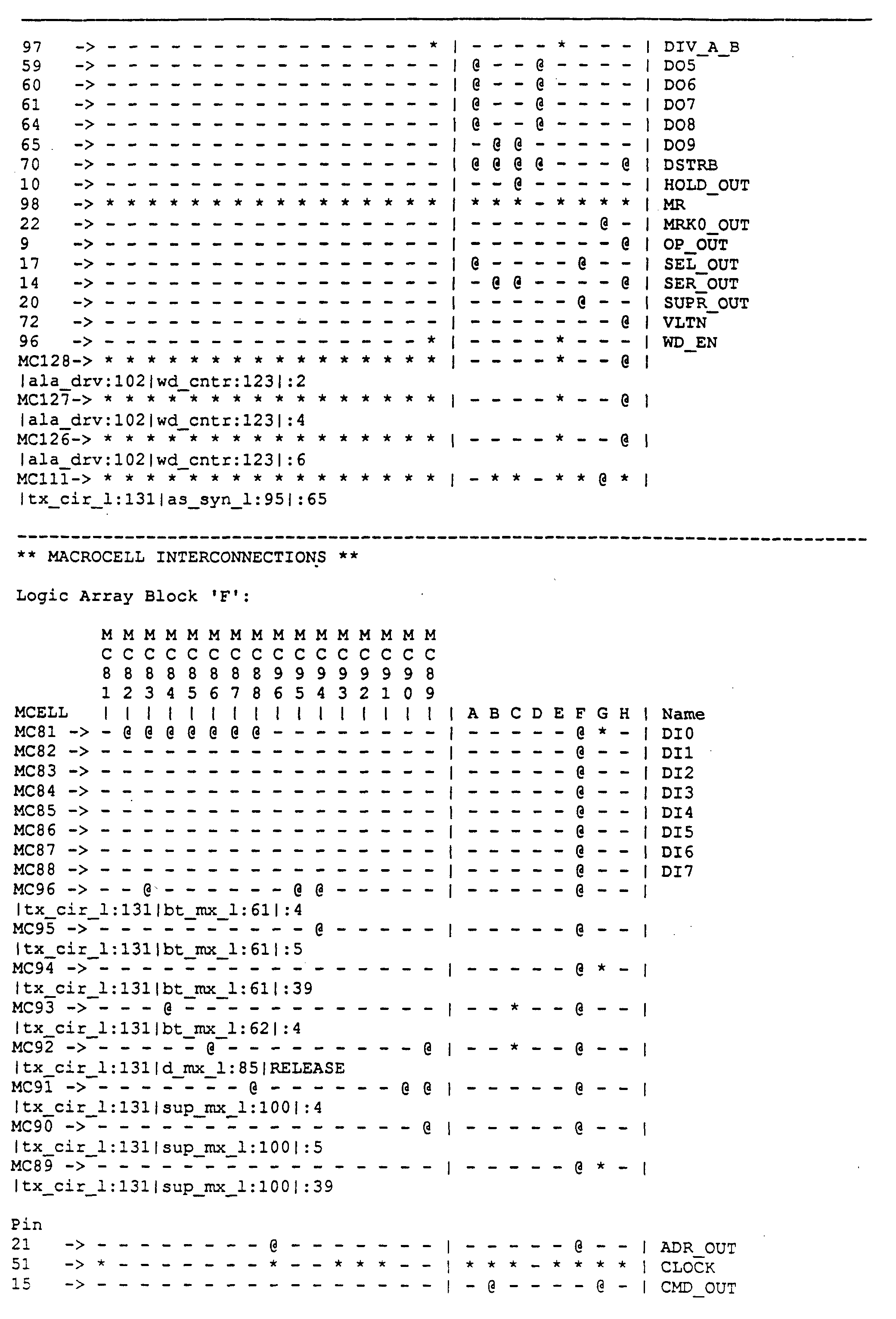
Two report files generated by a Max+Plus II Compiler for an EPM5130WC-1 chip from Altera Corp. are included in Appendices A and B to this specification and appear
immediately before the claims. The report files in
Appendices A and B show how embodiments of the EPLD 210 in each one of the adapters 114 and 115, respectively, can be implemented. These report files are sufficient information for one of ordinary skill in the art to reproduce the designs of these embodiments.
Alternatively, the multiplexing and demultiplexing means 210 can include a nonerasable programmable logic device (PLD) or a custom design programmable logic device, such as an application specific Integrated circuit (ASIC). If an ASIC is used, it can be designed to perform other functions than those included in the EPLD. For instance, such other functions can include the functions performed by any or all other components on the print circuit board 190. Such alternatives are equivalent to the embodiments
disclosed in more detail using the EPLD. The structure for performing the functions performed by any or all components on the print circuit board 190 can be referred to as integrated circuit means.
The integrated circuit means can include a transmitter section 213 and a receiver section 217.
The bus 211 of parallel traces connects the programmed EPLD 210 to a serializer 212 within the transmitter section 213. The serializer 212 converts parallel data to serial data. More specifically, the serializer 212 receives a plurality of parallel multiplexed signals from the 10-bit
bus 211 and sends it to an encoder latch to convert the 10- bit bus to a 12-bit encoded word. This encoding is used to maximize bit boundary transitions to help balance the data pattern and aid in the timing recovery on the receiving side. The 12-bit word is then fed to a shift register where the contents are serially shifted out in a single stream on one line. The serializer 212 can be a
transparent asynchronous transmitter-receiver interface (TAXI) commercially available under part no. AM-7968 from Advanced Micro Devices with offices in Sunnyvale,
California. A quartz crystal oscillator and clock
generator 236 can provide a fixed clock frequency to the serializer 212. In summary, the serializer 212 encodes the data, serializes it, converts the data to emitter coupled logic (ECL) levels (which are voltage signals), and shifts the data out over balanced lines. This data is fed to an ECL to current translator 214 which feeds current pulses to the transmitter connector 216 which can contain a light emitting diode device. The transmitter connector 216 connects to the connector on the end of the cable assembly 106 to send optical data pulses over one 107 of the fiber optic lines in the cable assembly 106. Alternatively, current data pulses from the ECL to current translator 214 are fed through an electrical transmitter connector and an electrical line of the electrical cable assembly 106.
Signals or data pulses are transmitted over line 109 of the cable assembly 106 and received by the receiver section 217. If the cable assembly 106 is fiber optic, the receiver section 217 includes the receiver connector 222 which can be a photodiode and preamplifier which converts groups of photons or optical light pulses to an analog voltage output . The photodiode and preamplifier 222 can be a positive intrinsic negative (PIN) photodiode and
preamplifier, such as, commercially available under part no. HFBR2614TC from Hewlett Packard. The output from the photodiode and preamplifier 222 is fed into a data
quantizer 220 which amplifies and converts the voltage signals to a constant level output that is ECL compatible.
The data quantizer 220 also provides a status indication or a loss of signal to the EPLD 210 indicating whether there is a connection at the distal end of the cable assembly 106. The data quantizer 220 can be part no. NE5224
commercially available from Signetics with offices in
Sunnyvale, California. The output of the data quantizer 220 is fed into a deserializer 218 which receives and the serialized ECL levels and continuously deserializes, decodes and latches parallel data through the 10 bit parallel bus 219 to the EPLD 210. The deserializer 218 can be part no. AM7969 commercially available from Advanced Micro Devices.
One or more voltage regulator 224,226,228,230,232 can be connected to provide a constant voltage supply to the line drivers/receivers 202,206, the EPLD 210, the
serializer 212 and the deserializer 218. The voltage regulators can be connected to a power input circuit 234 which can be "OR" connected to redundant power supplies 108. Thus, if the primary power supply 108 fails, power is automatically supplied from a second power supply 108.
Thus, data inputted to the bus and tag sub-assembly 102 from the bus and tag interfaces 12 and 13 is
transmitted over the dual line cable assembly 106 and the bus and tag sub-assembly 104 and appears at the receiving device interfaces 12 and 14 exactly duplicated, only delayed in the time domain by the seralization and deserialization function and the propagation delay of the pulses in the lines which is length dependent
(approximately 5 microseconds for each kilometer of optical fiber).
Figures 10-12 are block diagrams illustrating second, third and fourth embodiments of apparatus 100A, 100B and 100C for connecting one computer device 2 to another computer device 4 in accordance with the present invention. Figure 10 illustrates the apparatus 100A similar to the apparatus 100 illustrated in Figure 2 , except the converter adapters 114A, 115A are connected directly to the connectors 110A, 111A connected to bus interfaces 12, rather than to
the connectors 116A, 117A connected to the tag interfaces 14.
Figure 11 illustrates an apparatus 100B similar to the apparatus 100 illustrated in Figure 2, except the functions performed by the converter adapters 114 and 115 in Figure 2 are now performed by converter adapters 114B, 114B', 115B and 115B' which are connected directly to the connectors HOB, 116B, 111B and 117B, respectively. One of the cable assemblies 112 interconnects adapters 114B and 114B'.
Another one of the cable assemblies 112 interconnects adapters 115B and 115B'. Each pair of the converter adapters 114B,114B' and 115B,115B' include integrated circuit means similar to the one previously described in detail in relation to the embodiment illustrated in Figure 9, but with parts located in two housings rather than one. In the embodiment depicted in Figure 11, the integrated circuit means in converter adapters 114B,114B' is for (1) multiplexing and then serializing parallel bus and tag information received from the first and second interfaces 12,14 in the first device 2 and sending such multiplexed serial information over a first line of the dual line cable assembly 106 to the second computer device 4 and (2) deserializing and then demultiplexing serial bus and tag information received through a second line of the dual line cable assembly 106 and sending such parallel and
demultiplexed information to the first and second
interfaces 12,14 of the first device 2. In other words, the result achieved by converter adapter 114 in Figure 2 is achieved by converter adapters 114B and 114B' in Figure 11. Similarly, the result achieved by converter adapter 115 in Figure 2 is achieved by converter adapters 115B and 115B' in Figure 11.
Figure 12 illustrates the apparatus 100C similar to the apparatus 100 illustrated in Figure 2, except a
converter adapter 114C, 114C', 115C, 115C' is attached to each of the four connectors HOC, 114C, 111C, 117C connected to the interfaces 12,14 of the devices 2,4. This is like the apparatus 100B in Figure 11 in that each pair of the
converter adapters 114C,114C and 115C,115C include integrated circuit means similar to the one previously described in detail in relation to the embodiment
illustrated in Figure 9, but with parts located in two housings rather than one. Further, a dual line cable assembly 106 interconnects both bus converter adapters 114C,115C and a dual line cable assembly 106 interconnects both tag converter adapters 114C',115C'. In the embodiment depicted in Figure 12, the integrated circuit means in converter adapters 114C,114C is for (1) multiplexing and then serializing parallel bus and tag information received from the first and second interfaces 12,14 in the first device 2 and sending such multiplexed serial information over lines of the dual line cable assemblies 106 to the second computer device 4 and (2) deserializing and then demultiplexing serial bus and tag information received through other lines of the dual line cable assemblies 106 and sending such parallel and demultiplexed information to the first and second interfaces 12,14 of the first device 2. In other words, the result achieved by converter adapter 114 in Figure 2 is achieved by converter adapters 114C and 114C in Figure 12. Similarly, the result achieved by converter adapter 115 in Figure 2 is achieved by converter adapters 115C and 115C in Figure 12.
Each one of apparatuses 100A, 100B and 100C are defined as equivalent in function and structure to, and obtain the same result as, the apparatus 100.
The apparatus 100, 100A, 100B, 100C of the present invention can also interconnect daisy-chained peripheral control units on one mainframe multiplexer channel.
The apparatus of the present invention provides up to 4.5 million bytes per second of data throughput between the mainframe and peripherals. It also allows distances up to 2,000 meters (6600 feet) between devices - mainframe to peripheral, and/or peripheral to peripheral.
These features allow a user to replace bulky, limited distance bus and tag cables with dual line fiber optic or electrical cables in a structured wiring scheme. Data
transmission via fiber optic cables provides significant advantages over data transmission via conventional copper conductor (bus and tag) cables. There is less bulk and weight. They eliminate the need for raised computer room flooring, except potentially for cooling purposes. There is no electromagnetic or radio frequency interference with signals transmitted through fiber optic cables. There is greater data integrity and security since fiber optic cables are not easily tapped or monitored. Finally, the transmission distance is greater - up to 6600 feet versus 400 feet for conventional bus and tag cables. Those skilled in the art, having the benefit of the teachings of the present invention as hereinabove set forth, can effect numerous modifications thereto. These modifications are to be construed as being encompassed within the scope of the present invention as set forth in the appended claims.
APPEND IX A
Project Information f:\max2work\mini\mini_loc\mini_loc.rpt
MAX+plus II Compiler Report File
Version 2.11 04/06/92
***** Project compiled without errors
Title: LOCAL MINI-EXTENDER
Company: FiberCom, Inc.
Designer: Richard LaBarbera
Rev: A
Date: 3:35p 5-28-1992
** DEVICE SUMMARY **
Chip/ Input Output Bidir Shareable
POF Device Pins Pins Pins MCs EXPs % Utilized
MINI EPM5130WC-1 36 35 0 122 45 95 %
- - - - - - - - - - - - - - - - - - - - - - - - - - - - - - - - - - - - - - - - - - - - - - - - - - - - - - - - - - - - - - - - - - - - - - - - - ** PIN/MC/CHIP ASSIGNMENTS **
Actual
User Assignments
Assignments (if different) Node Name
MINI@85 ACKNLDGE
MINI@99 ACTIVITY
MINI@7 ADR_IN
MINI@21 ADR_OUT
MINI@40 BUS_INP
MINI@50 BUS_INO
MINI@49 BUS_IN1
MINI@48 BUS_IN2
MINI@47 BUS_IN3
MINI@46 BUS_IN4
MINI@45 BUS_IN5
MINI@42 BUS_IN6
MINI@41 BUS_IN7
MINI@29 BUS_OUTP
MINI@39 BUS_OUT0
MINI@36 BUS_OUT1
MINI@35 BUS_OUT2
MINI@34 BUS_OUT3
MINI@33 BUS_OUT4
MINI@32 BUS_OUT5
MINI@31 BUSJDUT6
MINI830 BUS_OUT7
MINI@51 CLOCK
MINI@15 CMD_OUT
MINI@84 COO
MINI883 CO1
MINI@3 DATA_IN
MINI@11 DATA_OUT
MINI@1 DISC_IN
MINI@97 DIV_A_B
MINI@73 DI0
MINI@74 DI1
MINI@75 DI2
MINI@76 DI3
MINI@77 DI4
MINI@78 DI5
MINI@79 DI6
MINI@80 DI7
MINI@81 DI8
MINI@82 DI9
MINI@54 DO0
MINI@55 DO1
MINI@56 DO2
MINI@57 DO3
MINI@58 DO4
MINI@59 DO5
MINI@60 DO6
MINI@61 DO7
MINI@64 DO8
MINI@65 DO9
MINI@28 DRV_OE
MINI@70 DSTRB
MINI@100 FAULT
MINI@10 HOLD_OUT
MINI@52 LOS
MINI@98 MR
MINI823 MRK0_IN
MINI@22 MRK0_OUT
MINI@8 OP_IN
MINI@9 OP_OUT
MINI@2 REQ_IN
MINI827 RLY_DRV
MINI@6 SEL_IN
MINI@17 SEL_OUT
MINI@4 SER_IN
MINI@14 SER_OUT
MINI@5 STAT_IN
MINI886 STROBE
MINI820 SUPR_OUT
MINI@72 VLTN
MINI896 WD_EN
- - - - - - - - - - - - - - - - - - - - - - - - - - - - - - - - - - - - - - - - - - - - - - - - - - - - - - - - - - - - - - - - - - - - - - - - - - - - - - - -
** FILE HIERARCHY **
|rx_cir_1 : 80|
|rx_cir_1 : 80|ds_det_1 : 47|
|rx_cir_ 1 : 80|si_dmx_1 : 93|
|rx_cir_1 : 80|ds_dmx_1 : 77|
|rx_cir_1 : 80|ds_dmx_1 : 78|
|rx__cir_1 : 80|bt_dmx 1 : 80|
|rx_cir_1 : 80|bt_dmx_1 : 82|
|rx_cir_1 : 80|bt_dmx_1 : 76|
|rx_cir_1 : 80|bt_dmx_1 : 75|
|rx_cir_1 : 80|bt_dmx_1 : 74|
|rx_cir_1 : 80|bt_dmx_1 : 73|
|tx]_cir_1 : 131|
|tx_cir_1 : 131|bt_mx_1 : 59|
|tx_cir_1 : 131|bt_mx_1 : 59|fclatch:51|
|tx_cir_1 : 131|sup_mx_1 : 100|
|tx_cir_1 : 131|sup_mx_1 : 100|fclatch:51|
|tx_cir_1 : 131|c_mx_1 : 94|
|tx_cir_1 : 131|c_mx_1 : 94|fclatch:96|
|tx_cir_1 : 131|ds_mx_1 : 89|
|tx_cir_1 : 131|c_mx_1 : 88|
|tx_cir_1 : 131|c_mx_1 : 88|fclatch:92|
|tx_cir_1 : 131|d_mx_1 : 85|
|tx_cir_1 : 131|c_mx_1 : 85|fclatch:93|
|tx_cir_1 : 131|as_syn_1 : 95|
|tx_cir_1 : 131|ds_mx_1 : 61|
|tx_cir_1 : 131|ds_mx_1 : 61|fclatch:51|
| tx_cir_1 : 131 | bt_mx_1 : 62 |
| tx_cir_1 : 131 | bt_mx_1 : 62 | fclatch : 51
| tx_cir_1 : 131 | bt_mx_1 : 65 |
| tx_cir_1 : 131 | bt_mx_1 : 65 | fclatch: 51 |
| tx_cir_1 : 131 | bt_mx_1 : 66 |
| tx_cir_1 : 131 | bt_mx_1 : 66 | fclatch: 51 |
| ala_drv:102|
| ala drv:102|wd cntr:123|
- - - - - - - - - - - - - - - - - - - - - - - - - - - - - - - - - - - - - - - - - - - - - - - - - - - - - - - - - - - - - - - - - - - - - - - - - - - - - - - -
***** Logic for device 'MINI' compiled without errors
Device: EPM5130WC-1
Security: OFF
A R R R R R A
C D E E E E E C
T I S S S S S S K
F I V W E E E E E T N
A V _ D R R R R R R L
U I A _ V V V V V V V G G O D C C D D
L T M _ E E C C E E E E N N B G O O I I
T Y R B N D C C D D D D D E E 0 1 9 8
- - - - - - - - - - - - - - - - - - - - - - - - - - - - - - - - - - - - - - - - - - - - - - - - - - - - - - - - - - -
/ 100 99 98 97 96 95 94 93 92 91 90 89 88 87 86 85 84 83 82 81 |
DISC_IN | 1 80 | DI7
REQ_IN | 2 79 | DI6
DATA_IN | 3 78 | DI5
SER_IN | 4 77 | DI4
STAT_IN | 5 76 | DI3
SEL_IN | 6 75 | DI2
ADR_IN | 7 74 | DI1
OP_IN | 8 73 | DI0
OP_OUT | 9 72 | VLTN
HOLD_OUT | 10 71 | GND
DATA OUT | 11 70 | DSTRB
GND | 12 69 | VCC
GND | 13 68 | VCC
SER_OUT | 14 67 | GND
CMD_OUT | 15 66 | GND
GND | 16 EPM5130WC-1 65 | DO9
SEL OUT | 17 64 | DO8
VCC | 18 63 | GND
VCC | 19 62 | GND
SUPR_OUT | 20 61 | DO7
ADR_OUT | 21 60 | DO6
MRK0_OUT | 22 59 | DO5
MRK0_IN | 23 58 | DO4
RESERVED | 24 57 | DO3
RESERVED | 25 56 | DO2
RESERVED | 26 55 | DO1
RLY_DRV | 27 54 | DO0
DRV_OE | 28 53 | RESER
BUS_OUTP | 29 52 | LOS
BUS_OUT7 | 30 51 | CLOCK
|_ 31 32 33 34 35 36 37 38 39 40 41 42 43 44 45 46 47 48 49 50 |
- - - - - - - - - - - - - - - - - - - - - - - - - - - - - - - - - - - - - - - - - - - - - - - - - - - - - - - - - - - - - - -
B B B B B B G G B B B B V V B B B B B B
U U U U U U N N U U U U C C U U U U U U
S S S S S S D D S S S s e c S S s S S S
_ _ _ _ _ _ _ _ _ _ _ _ _ _ _ _
O O O O O O O I I I I I I I I I
U U U U U U U N N N N N N N N N
T P 7 6 5 4 3 2 1 0
6 5 4 3 2 1 0
** RESOURCE USAGE **
Shareable External
Logic Array Block Macrocells I/O Pins Expanders Interconnect
A: MC1 - MC16 12/16( 75%) 8/ 8(100%) 8/32 ( 25%) 14/24 ( 58%)
B: MC17 - MC32 14/16( 87%) 5/ 8( 62%) 2/32 ( 6%) 9/24 ( 37%)
C: MC33 - MC48 16/16(100%) 8/ 8(100%) 29/32 ( 90%) 18/24 ( 75%)
D: MC49 - MC64 16/16(100%) 8/ 8(100%) 0/32 ( 0%) 7/24 ( 29%)
E: MC65 - MC80 16/16(100%) 7/ 8( 87%) 1/32 ( 3%) 8/24 ( 33%)
F: MC81 - MC96 16/16(100%) 8/ 8(100%) 0/32 ( 0%) 14/24 ( 58%)
G: MC97 - MC112 16/16(100%) 6/ 8( 75%) 3/32 ( 9%) 17/24 ( 70%)
H: MC113 - MC128 16/16(100%) 5/ 8( 62%) 2/32 ( 6%) 10/24 ( 41%)
Total dedicated input pins used: 16/ 20 ( 80%)
Total I/O pins used: 55/ 64 ( 85%)
Total macrocells used: 122/128 ( 95%)
Total shareable expanders used: 45/256 ( 17%)
Total input pins required: 36
Total output pins required: 35
Total bidirectional pins required: 0
Total macrocells required: 122
Total shareable expanders in database: 45
Synthesized macrocells: 0/128 ( 0%)
- - - - - - - - - - - - - - - - - - - - - - - - - - - - - - - - - - - - - - - - - - - - - - - - - - - - - - - - - - - - - - - - - - - - - - - - - - - - - - -
** INPUTS **
Expanders Fan-In
Pin MCell LAB Primitive Total Shared INP FBK Name
85 (101) (G) INPUT 0 0 0 0 ACKNLDGE
21 - - INPUT 0 0 0 0 ADR_OUT
29 (23) (B) INPUT 0 0 0 0 BUS_OUTP
39 (39) (C) INPUT 0 0 0 0 BUS_OUT0
36 (38) (C) INPUT 0 0 0 0 BUS_OUT1
35 (37) (C) INPUT 0 0 0 0 BUS_OUT2
34 (36) (C) INPUT 0 0 0 0 BUS_OUT3
33 (35) (C) INPUT 0 0 0 0 BUS_OUT4
32 (34) (C) INPUT 0 0 0 0 BUS_OUT5
31 (33) (C) INPUT 0 0 0 0 BUS_OUT6
30 (24) (B) INPUT 0 0 0 0 BUS_OUT7
51 (65) (E) INPUT 0 0 0 0 CLOCK
15 - - INPUT 0 0 0 0 CMD_OUT
11 - - INPUT 0 0 0 0 DATA_OUT
97 (117) (H) INPUT 0 0 0 0 DIV_A_B
54 (68) (E) INPUT 0 0 0 0 DO0
55 (69) (E) INPUT 0 0 0 0 DO1
56 (70) (E) INPUT 0 0 0 0 DO2
57 (71) (E) INPUT 0 0 0 0 DO3
58 (72) (E) INPUT 0 0 0 0 DO4
59 - - INPUT 0 0 0 0 DO5
60 - - INPUT 0 0 0 0 DO6
61 - - INPUT 0 0 0 0 DO7
64 - - INPUT 0 0 0 0 DO8
65 - - INPUT 0 0 0 0 DO9
70 - - INPUT 0 0 0 0 DSTRB
10 - - INPUT 0 0 0 0 HOLD_OUT
52 (66) (E) INPUT 0 0 0 0 LOS
98 (118) (H) INPUT 0 0 0 0 MR
22 - - INPUT 0 0 0 0 MRK0_OUT
9 - - INPUT 0 0 0 0 OP_OUT
17 - - INPUT 0 0 0 0 SEL_OUT
14 - - INPUT 0 0 0 0 SER_OUT
20 - - INPUT 0 0 0 0 SUPR_OUT
72 - - INPUT 0 0 0 0 VLTN
96 (116) (H) INPUT 0 0 0 0 WD_EN
- - - - - - - - - - - - - - - - - - - - - - - - - - - - - - - - - - - - - - - - - - - - - - - - - - - - - - - - - - - - - - - - - - - - - - - - - - - - - - -
** OUTPUTS **
Shareable
Expanders Fan-In
Pin MCell LAB Primitive Total Shared INP FBK Name
99 119 H OUTPUT 0 0 0 2 ACTIVITY
7 7 A DFF 0 0 4 0 ADR IN
40 40 C DFF 0 0 1 3 BUS_INP
50 56 D DFF 0 0 1 3 BUS_IN0
49 55 D DFF 0 0 1 3 BUS_IN1
48 54 D DFF 0 0 1 3 BUS_IN2
47 53 D DFF 0 0 1 3 BUS_IN3
46 52 D DFF 0 0 1 3 BUS_IN4
45 51 D DFF 0 0 1 3 BUS_IN5
42 50 D DFF 0 0 1 3 BUS_IN6
41 49 D DFF 0 0 1 3 BUS_IN7
84 100 G OUTPUT 0 0 1 0 COO
83 99 G OUTPUT 0 0 1 0 CO1
3 3 A DFF 0 0 4 1 DATA_IN
1 1 A DFF 0 0 4 0 DISC_IN
73 81 F DFF 0 0 2 1 DI0
74 82 F OUTPUT . 0 0 0 3 DI1
75 83 F OUTPUT 0 0 0 3 DI2
76 84 F OUTPUT 0 0 0 3 DI3
77 85 F OUTPUT 0 0 0 3 DI4
78 86 F OUTPUT 0 0 0 3 DI5
79 87 F OUTPUT 0 0 0 3 DI6
80 88 F OUTPUT 0 0 0 3 DI7
81 97 G OUTPUT 0 0 0 3 DI8
82 98 G OUTPUT 0 0 0 3 DI9
28 22 B OUTPUT 0 0 1 0 DRV_OE
100 120 H OUTPUT 0 0 1 1 FAULT
23 17 B DFF 0 0 4 0 MRK0_IN
8 8 A DFF 0 0 4 0 OP_IN
2 2 A DFF 0 0 4 0 REQ_IN
27 21 B OUTPUT 0 0 1 0 RLY_DRV
6 6 A MCELL 0 0 0 2 SEL_IN
4 4 A DFF 0 0 4 1 SER_IN
5 5 A DFF 0 0 4 0 STAT_IN
86 102 G DFF 1 0 2 13 STROBE
- - - - - - - - - - - - - - - - - - - - - - - - - - - - - - - - - - - - - - - - - - - - - - - - - - - - - - - - - - - - - - - - - - - - - - - - - - - - - -
** BURIED LOGIC **
Shareable
Expanders Fan-In
Pin MCell LAB Primitive Total Shared INP FBK Name
- 128 H DFF 2 1 | ala_drv: 102 | wd_cntr: 123 | :2 - 127 H DFF 2 2 |ala_drv: 102 | wd_cntr: 123 | :4 - 80 E DFF 2 18 | ala_drv: 102 | wd_cntr: 123 | :5 - 126 H DFF 2 3 |ala_drv: 102 |wd_cntr: 123 | :6 - 79 E DFF 2 4 |ala_drv; 102 | wd_cntr: 123 | :7 - 78 E DFF 2 5 | ala_drv: 102 | wd_cntr: 123 | :8 - 77 E DFF 2 6 |ala_drv: 102 | wd_cntr: 123 | :9 - 76 E DFF 2 7 | ala_drv: 102 | wd_cntr: 123 | :10 - 75 E DFF 2 8 |ala_drv: 102 | wd_cntr: 123 | :11 - 74 E DFF 2 9 | ala_drv: 102 | wd_cntr: 123| :12 - 73 E DFF 2 10 |ala_drv: 102 | wd_cntr: 123 | :13
(58) 72 E DFF 2 11 |ala_drv: 102 | wd_cntr: 123 | :14 (57) 71 E DFF 2 12 |ala_drv: 102 |wd cntr: 123 | :15
(56) 70 E DFF 0 0 2 13 ala_drv: 102 |wd_cntr: 123 | :16
(55) 69 E DFF 0 0 2 14 ala_drv:102 | wd_cntr: 123 | :17
(54) 68 E DFF 0 0 2 15 ala_drv: 102 |wd_cntr: 123| :18
(52) 66 E DFF 0 0 2 16 ala_drv:102 |wd_cntr:123 | :19
(51) 65 E DFF 0 0 2 17 ala_drv: 102 |wd_cntr: 123| :20
(53) 67 E DFF 1 0 4 19 ala_drv : 102 | WD_SEND
- 125 H DFF 1 1 1 7 ala_drv:102|:2
- 124 H DFF 1 1 2 5 ala_drv:102|:3
- 123 H DFF 1 1 2 5 ala_drv:102|:96
- 48 C DFF 0 0 3 2 rx_cir_1 : 80 | bt_dmx_1 : 73 | : 2
- 64 D DFF 0 0 3 2 rx_cir_1 : 80 | bt_dmx_1 : 74 | : 2
- 63 D DFF 0 0 3 2 rx_cir_1 : 80 | bt_dmx_1 : 75 | : 2
- 62 D DFF 0 0 3 2 rx_cir_1 : 80 | bt_dmx_1: 76 | : 2
- 61 D DFF 0 0 3 2 rx_cir_1 : 80 | bt_dmx_1: 80 | : 2
- 60 D DFF 0 0 3 2 rx_cir_1 : 80 | bt_dmx_1: 82 | : 2
- 32 B DFF 1 0 1 4 rx_cir_1 : 80 | ds_det_1 : 47 | : 2
- 31 B DFF 0 0 1 4 rx_cir_1 : 80 | ds_det_1: 47 | : 3
- 59 D DFF 0 0 3 2 rx_cir_1 : 80 | ds_dmx_1 : 77 | : 2
- 30 B DFF 0 0 2 2 rx_cir_1 : 80 | ds_dmx_1: 77 | : 26
- 58 D DFF 0 0 3 2 rx_cir_1 : 80 | ds_dmx_1 : 78 | : 2
- 29 B DFF 0 0 2 2 rx_cir_1 : 80 | ds_dmx_1: 78 | : 26
- 57 D DFF 0 0 3 2 rx_cir_1 : 80 | sl_dmx_1 : 93 | : 2
- 16 A DFF 0 0 4 0 rx_cir_1 : 80 | sl_dmx_1: 93 | : 3
- 15 A DFF 0 0 2 1 rx_cir_1 : 80 | sl_dmx_1: 93 | : 20
- 28 B DFF 0 0 0 2 rx_cir_1:80| :84
- 27 B DFF 0 0 0 2 rx_cir_1:80| :85
- 26 B DFF 0 0 1 2 rx_cir_1:80| :86
- 112 G DFF 0 0 2 13 tx_cir_1 : 131 | as_syn_1 : 95 | : 58
- 111 G DFF 1 0 1 14 tx_cir_1:131 |as_syn_1:95 | :65
- 122 H DFF 0 0 3 1 tx_cir_1 : 131 | bt_mx_1: 59 | : 4
- 121 H DFF 0 0 1 2 tx_cir_1 : 131 | bt_mx_1: 59 | : 5
(98) 118 H SOFT 0 0 0 2 tx_cir_1 : 131 | bt_mx_1 : 59 | : 39
- 47 C DFF 4 0 3 3 tx_cir_1 : 131 | bt_mx_1 : 59 | : 45
- 96 F DFF 0 0 3 1 tx_cir_1 : 131 | bt_mx_1 : 61 | : 4
- 95 F DFF 0 0 1 2 tx_cir_1 : 131 | bt_mx_1 : 61 | : 5
- 94 F SOFT 0 0 0 2 tx_cir_1 : 131 | bt_mx_1: 61 | : 39
- 46 C DFF 4 0 3 3 tx_cir_1 : 131 | bt_mx_1 : 61 | : 45
- 93 F DFF 0 0 3 1 tx_cir_1 : 131 | bt_mx_1: 62 | : 4
- 45 C DFF 0 0 1 2 tx_cir_1 : 131 | bt_mx_1 : 62 | : 5
- 44 C SOFT 0 0 0 2 tx_cir_1 : 131 | bt_mx_1: 62 | : 39
- 43 C DFF 4 0 3 3 tx_cir_1 : 131 | bt_mx_1 : 62 | : 45
- 42 C DFF 0 0 3 1 tx_cir_1 : 131 | bt_mx_1: 65 | : 4
- 110 G DFF 0 0 1 2 tx_cir_1 : 131 | bt_mx_1 : 65 | : 5
- 109 G SOFT 0 0 0 2 tx_cir_1 : 131 | bt_mx_1: 65 | : 39
- 41 C DFF 4 0 3 3 tx_cir_1 : 131 | bt_mx_1: 65 | : 45
- 108 G DFF 0 0 3 1 tx_cir_1 : 131 | bt_mx_1: 66 | : 4
- 107 G DFF 0 0 1 2 tx_cir_1 : 131 | bt_mx_1 : 66 | : 5
- 106 G SOFT 0 0 0 2 tx_cir_1 : 131 | bt_mx_1: 66 | : 39
(39) 39 C DFF 4 0 3 3 tx_cir_1 : 131 | bt_mx_1 : 66 | : 45
- 105 G DFF 0 0 3 1 tx_cir_1 : 131 | c_mx_1 : 94 | : 4
(85) 101 G DFF 1 1 1 3 tx_cir_1 : 131 | c_mx_1 : 94 | : 57
(90) 104 G DFF 0 0 2 2 tx_cir_1 : 131 | c_mx_1 : 94 | : 79
(36) 38 C DFF 4 0 3 3 tx_cir_1 : 131 | c_mx_1 : 94 | : 86
(89) 103 G DFF 1 1 1 4 tx_cir_1 : 131 | c_mx_1 : 94 | : 89
- 92 F DFF 0 0 3 1
tx_cir_1:131|d_mx_1:85| RELEASE
(35) 37 C DFF 1 0 1 3 tx_cir_1:13l | d_mx_1:85| SEND
(34) 36 C DFF 0 0 2 1 tx_cir_1:131 | d_mx_1:85|:79
(33) 35 C DFF 4 0 3 3 tx_cir_1:131 | d_mx_1:85| : 86
- 25 B DFF 1 0 5 4 tx_cir_1:131 | ds mx_1:89| SEND
(30) 24 B DFF 0 0 4 1 tx_cir_1:131 | ds_mx_1:89| :105
(29) 23 B DFF 0 0 4 2 tx_cir_1:131 | ds_mx_1:89| :106
(32) 34 C DFF 0 0 1 2 tx_cir_1:131 | ds_mx_1:89| :116
(31) 33 C DFF 0 0 1 2 tx_cir_1:131 | ds_mx_1:89|:117
(26) 20 B DFF 0 0 2 2 |tx_cir_1:131|ds_mx_1:89|:128
(97) 117 H DFF 0 0 3 1
|tx_cir_1:131| s_mx_1 :88|RELEASE
(96) 116 H DFF 1 1 1 3 |tx_cir_1:131|s_mx_1:88|:57
(95) 115 H DFF 0 0 2 2 |tx_cir_1:131|s_mx_1:88|:58
(92) 114 H DFF 1 1 1 4 |tx cir_1:131|s_mx_1:88|:74
(91) 113 H DFF 0 0 1 2 |tx_cir_1:131|s_mx_1:88|:75
- 14 A DFF 4 0 3 3 |tx cir_1:131|s_mx_1:88|:84
- 91 F DFF 0 0 3 1 |tx_cir_1:131|sup mx_1:100|:4
- 90 F DFF 0 0 1 2 |tx_cir_1:131|supmx_1:100|:5
- 89 F SOFT 0 0 0 4 |tx_cir_1:131|supmx_1:100|:39
- 13 A DFF 4 0 3 3 |tx_cir_1:131|sup_mx_1:100|:45 - - - - - - - - - - - - - - - - - - - - - - - - - - - - - - - - - - - - - - - - - - - - - - - - - - - - - - - - - - - - - - - - - - - - - - - - - - - - - -
** MACROCELL INTERCONNECTIONS **
Logic Array Block 'A ' :
M M M M M M M M M M M M
C C C C C C C C C C C C
7 3 1 8 2 1 1 6 4 5 1 1
| | | | | 6 5 | | | 4 3
MCELL | | | | | | | | | | | | A B C D E F G H | Name
MC7 -> @ - - - - - - - - - - - | @ - - - - - - - | ADR_IN
MC3 -> - @ - - - - - - - - - - | @ * - - - - - - | DATA_IN
MC1 -> - - @ - - - - - - - - - | @ - - - - - - - | DISC_IN
MC8 -> - - - @ - - - - - - - - | @ * - - - - - - | OP_IN
MC2 -> - - - - @ - - - - - - - | @ - - - - - - - | REQ_IN
MC16 -> - - - - - @ @ @ - - - - | @ - - - - - - - | |rxcir_1:80|sl_dmx_1:93|:3 MC15 -> - - - - - - - @ - - - - | @ - - - - - - - |
|rx_cir_1:80|sl_dmx_1:93|:20
MC6 -> - - - - - - - - - - - - | @ - - - - - - - | SEL_IN
MC4 -> - - - - - - - - @ - - - | @ * - - - - - - | SER_IN
MC5 -> - - - - - - - - - @ - - | @ * - - - - - - | STAT_IN
MC14 -> - - - - - - - - - - - - | @ - - - - - - - | |tx_cir_1:131|s_mx_1:88|:84 MC13 -> - - - - - - - - - - - - | @ - - - - - - - |
|tx_cir_1:131|sup_mx_1:100|:45
Pin
21 -> - - - - - - - - - - - - | - - - - - @ - - | ADR_OUT
34 -> - - - - - - - - - - * - | * - - - - - - - | BUS_OUT3
31 -> - - - - - - - - - - - * | * - - - - @ - - | BUS_OUT6
51 -> - - - - - - - - - - * * | * * * - * * * * | CLOCK
15 -> - - - - - - - - - - - - | - @ - - - - @ - | CMD_OUT
11 -> - - - - - - - - - - - - | - - - - - @ - - | DATA_OUT
54 -> * * * * * * - - * * - - | * * * * - - - - | DO0
55 -> - - - - - - - - - - - - | * - - * - - - - | DO1
56 -> - - - - - - - - - - - - | * - - * - - - - | DO2
57 -> - - - - - - - - - - - - | * - - * - - - - | DO3
58 -> - - - - - - - - - - - - | * - - * - - - - | DO4
59 -> - - - - - - - - - - - - | @ - - @ - - - - | DO5
60 -> - - - - - - - - - - - - | @ - - @ - - - - | DO6
61 -> - - - - @ - - - - - - - | @ - - @ - - - - | DO7
64 -> - - @ - - - - - - - - - | @ - - @ - - - - | DO8
65 -> - - - - - - - - - - - - | - @ @ - - - - - | DO9
70 -> @ @ @ @ @ @ - -@ @ - - | @ @ @ @ - - - @ | DSTRB
10 -> - - - - - - - - - - - - | - - @ - - - - - | HOLD_OUT
98 -> * * * * * * * - * * * * | * * * - * * * * | MR
22 -> - - - - - - - - - - - - | - - - - - - @ - | MRK0_OUT
9 -> - - - - - - - - - - - - | - - - - - - - @ | OP_OUT
17 -> - - - - - - @ - - - - - | @ - - - - @ - - | SEL_OUT
14 -> - - - - - - - - - - - - | - @ @ - - - - @ | SERJDUT
20 -> - - - - - - - - - - - - | - - - - - @ - - | SUPR_OUT
72 -> - - - - - - - - - - - - | - - - - - - -@ | VLTN
MC30 -> - * - - - - - - - - - - | * @ - - - - - - | I rx cir 1 : 80 Ids dmx 1:77 | :26
MC102-> - - - - * - - - - - - - - - - - | - - - - - - @ * | STROBE
MC112-> - - - - - - - - * - - * - - - - | * - * - - * @ * |
| tx_cir_1 : 131 | as_syn_1 : 95 | : 58
MC111-> - * * * - - - - - * - - * - * - | - * * - * *@ * |
| tx_cir_1 : 131 | as_syn_1: 95 | : 65
** EQUATIO NS **
ACKNLDGE : INPUT;
ADR_OUT : INPUT;
BUS_OUTP : INPUT;
BUS_OUT0 : INPUT;
BUS_OUT1 : INPUT;
BUS_OUT2 : INPUT;
BUS_OUT3 : INPUT;
BUS_OUT4 : INPUT;
BUS_OUT5 : INPUT;
BUS_OUT6 : INPUT;
BUS_OUT7 : INPUT;
CLOCK : INPUT;
CMS_OUT : INPUT;
DATA_OUT : INPUT;
DIV_A_B : INPUT;
DO0 : INPUT;
DO1 : INPUT;
DO2 : INPUT;
DO3 : INPUT;
DO4 : INPUT;
DO5 : INPUT;
DO6 : INPUT;
DO7 : INPUT;
DO8 : INPUT;
DO9 : INPUT;
DSTRB : INPUT;
HOLD_OUT : INPUT;
LOS : INPUT;
MR : INPUT;
MRK0_OUT : INPUT;
OP_OUT : INPUT;
SEL_OUT : INPUT;
SER_OUT : INPUT;
SUPR_OUT : INPUT;
VLTN : INPUT;
WD_EN : INPUT;
ACTIVITY = _MC119;
_MC119 = MCELL ( _EQ001 $ VCC );
_EQ001 = !_MC124 & !_MC125;
% ADR_IN = |rx_cir_1:80|bt_dmx_1:80|TAG %
ADR_IN = _MC007;
_MC007 = DFF( _EQ002 $ GND, DSTRB, MR, VCC );
_EQ002 = DO0 & DO2
# !DO0 & _MC007;
% BUS_INP = | rx_cir_1:80 | bt_dmx_1 : 73 | : 17 %
BUS_INP = _MC040;
_MC040 = DFF( _MC048 $ GND, DSTRB, _EQ003, VCC );
_EQ003 = !_MC027 & !_MC028;
% BUS_IN0 = |rx_cir_1:80|bt_dmx_1:82|:17 %
BUS_IN0 = _MC056;
_MC056 = DFF( _MC060 $ GND, DSTRB, _EQ004, VCC );
_EQ004 = !_MC027 & !_MC028 ;
% BUS_IN1 = |rx_cir_1:80|bt_dmx_1:80|:17 %
BUS_IN1 = _MC055;
_MC055 = DFF( _MC061 $ GND, DSTRB, _EQ005, VCC ); _EQ005 = !_MC027 & !_MC028;
% BUS_IN2 = |rx_cir_1:80|sl_dmx_1:93|:17 %
BUS_IN2 = _MC054;
_MC054 = DFF( _MC057 $ GND, DSTRB, _EQ006, VCC ); _EQ006 = !_MC027 & !_MC028;
% BUS_IN3 = |rx_cir_1:80|ds_dmx_1:78|:33 %
BUS_IN3 = _MC053;
_MC053 - DFF( _MC058 $ GND, DSTRB, _EQ007, VCC ); _EQ007 = !_MC027 & !_MC028;
% BUS_IN4 = |rx_cir_1:80|ds_dmx_1:77| :33 %
BUS_IN4 = _MC052;
_MC052 = DFF( _MC059 $ GND, DSTRB, _EQ008, VCC ); _EQ008 = !_MC027 & !_MC028;
% BUS_IN5 = | rx_cir_1: 80 |bt_dmx_1 : 76 | : 17 %
BUS_IN5 = _MC051;
_MC051 = DFF( _MC062 $ GND, DSTRB, _EQ009, VCC );
_EQ009 = !_MC027 & !_MC028;
% BUS_IN6 = |rx_cir_1:80|bt_dmx_1:75| :17 %
BUS_IN6 = _MC050;
_MC050 = DFF( _MC063 $ GND, DSTRB, _EQ010, VCC ); _EQ010 = !_MC027 & !_MC028;
% BUS_IN7 = |rx_cir_1:80|bt_dmx_1:74| :17 %
BUS_IN7 = _MC049;
_MC049 = DFF( _MC064 $ GND, DSTRB, _EQ011, VCC ); _EQ011 = !_MC027 & !_MC028;
CO0 = _MC100;
_MC100 = MCELL ( !MR $ GND ) ;
COl = _MC099;
_MC099 = MCELL ( !MR $ GND ) ;
% DATA_IN = |rx_cir_1:80|ds_dmx_1:77|TAG %
DATA_IN = _MC003;
_MC003 = DFF( _EQ012 $ GND, DSTRB, _EQ013, VCC );
_EQ012 - DO0 & DO5
# !DO0 & _MC003;
_EQ013 = !_MC030 & MR;
% DISC_IN = |rx_cir_1:80|bt_dmx_1:74|TAG %
DISC_IN = _MC001;
_MC001 = DFF( _EQ014 $ GND, DSTRB, MR, VCC ); _EQ014 = DO0 & DO8
# !DO0 & _MC001;
% DI0 = |tx_cir_1:131|as_syn_1:95| :70 %
DI0 = _MC081;
_MC081 = DFF( _MC112 $ GND, CLOCK, MR, VCC );
DI1 = _MC082;
_MC082 = MCELL ( _EQ015 $ GND );
_EQ015 = _MC081 & _MC122
# _MC047 & !_MC081;
DI2 = _MC083;
_MC083 = MCELL ( _EQ016 $ GND );
_EQ016 = _MC081 & _MC096
# _MC046 & !_MC081;
DI3 = _MC084;
_MC084 = MCELL( _EQ017 $ GND ) ;
_EQ017 = _MC081 & _MC093
# _MC043 & !_MC081;
DI4 = _MC085;
_MC085 = MCELL ( _EQ018 $ GND );
_EQ018 = _MC081 & _MC117
# _MC014 & !_MC081;
DI5 = _MC086;
_MC086 = MCELL ( _EQ019 $ GND );
_EQ019 = _MC081 & _MC092
# _MC035 & !_MC081;
DI6 = _MC087;
_MC087 = MCELL ( _EQ020 $ GND );
_EQ020 = _MC081 & _MC105
# _MC038 & !_MC081;
DI7 = _MC088;
_MC088 = MCELL ( _EQ021 $ GND );
_EQ021 = _MC081 & _MC091
# _MC013 & !_MC081;
DI8 = _MC097;
_MC097 = MCELL ( _EQ022 $ GND );
_EQ022 = _MC042 & _MC081
# _MC041 & !_MC081;
DI9 = _MC098;
_MC098 = MCELL ( _EQ023 $ GND );
_EQ023 = _MC081 & _MC108
# _MC039 & !_MC081;
DRV_OE = _MC022;
_MC022 - MCELL ( ! LOS $ GND );
FAULT = _MC120;
_MC120 = MCELL ( _EQ024 $ _MC123 );
_EQ024 = LOS & !_MC123;
% MRK0_IN - |rx_cir_1:80|bt_dmx_1:73|TAG %
MRK0_IN = _MC017;
_MC017 = DFF( _FQ025 $ GND, DSTRB, MR, VCC ); _EQ025 = DO0 & DO9
# !DO0 & _MC017;
% OP_IN = |rx_cir_1:80|bt_dmx_1:82|TAG %
OP_IN = _MC008;
_MC008 = DFF( _EQ026 $ GND, DSTRB, MR, VCC ); _EQ026 = DO0 & DO1
# !DO0 & _MC008;
% REQ_IN = |rx_cir_1:80|bt_dmx_1:75|TAG %
REQ_IN = _MC002;
_MC002 = DFF{ _EQ027 $ GND, DSTRB, MR, VCC ); _EQ027 = DO0 & DO7
# !DO0 & _MC002;
RLY_DRV = _MC021;
_MC021 = MCELL( ! LOS $ GND );
% SEL_IN = |rx_cir_1:80|sl_dmx_1:93|:26 %
SEL_IN = _MC006;
_MC006 = MCELL ( _EQ028 $ GND );
_EQ028 = !_MC015 & _MC016;
% sER_IN - |rx_cir_1:80|ds_dmx_1:78|TAG %
SER_IN = _MC004;
_MC004 = DFF( _EQ029 $ GND, DSTRB, _EQ030, VCC );
_EQ029 = DO0 & DO4
# !DO0 & _MC004;
_EQ030 = !_MC029 & MR;
% STAT_IN = |rx_cir_1:80|bt_dmx_1:76|TAG %
STAT_IN = _MC005;
_MC005 = DFF( _FQ031 $ GND, DSTRB, MR, VCC );
_EQ031 = DO0 & DO6
# !DO0 & _MC005;
% STROBE = |tx_cir_l:131|as_syn_l:95|STRB %
STROBE = _MC102;
_MC102 = DFF( _EQ032 $ VCC, !CLOCK, _EQ033, VCC );
_EQ032 = _MC025 & _MC037 & _MC044 & _MC067 & _MC089 & _MC094 &
_MC101 & _MC103 - _MC106 & _MC109 & _MC114 & _MC116 & _MC118;
_EQ033 = _X001;
_X001 - EXP( ACKNLDGE & _MC102 );
% |ala_drv:102|wd_cntr:123|:2 %
_MC128 = DFF( VCC $ _MC128, CLOCK, _EQ034, VCC );
_EQ034 = !_MC111 & MR;
% |ala_drv:102|wd_cntr:123| :4 %
_MC127 = DFF( _MC128 $ _MC127, CLOCK, _EQ035, VCC );
_EQ035 = !_MC111 & MR;
% |ala_drv:102|wd_cntr:123| :5 %
_MC080 = DFF( _EQ036 $ _MC080, CLOCK, _EQ037, VCC );
_EQ036 = _MC065 - _MC066 & _MC068 & _MC069 & _MC070 & _MC071 &
_MC072 m _MC073 & _MC074 & _MC075 & _MC076 & _MC077 & _MC078 & _MC079 & _MC126 & _MC127 & _MC128;
_EQ037 = !_MC111 & MR;
% |ala_drv:102|wd_cntr:123|:6 %
_MC126 = DFF( _EQ038 $ _MC126, CLOCK, _EQ039, VCC );
_EQ038 = _MC127 & _MC128;
_EQ039 = !_MC111 & MR;
% |ala_drv:102|wd_cntr:123| :7 %
_MC079 = DFF( _EQ040 $ _MC079, CLOCK, _EQ041, VCC );
_EQ040 = _MC126 & _MC127 & _MC128;
_EQ041 = !_MC111 & MR;
% |ala_drv:102|wd_cntr:123| :8 %
_MC078 = DFF( _EQ042 $ _MC078, CLOCK, _EQ043, VCC );
_EQ042 = _MC079 & _MC126 & _MC127 & _MC128;
_EQ043 = !_MC111 & MR;
% |ala_drv:102|wd_cntr:123|:9 %
_MC077 = DFF( _EQ044 $ _MC077, CLOCK, _EQ045, VCC );
_EQ044 = _MC078 & _MC079 & MC126 & MC127 & MC128;
_EQ045 = ! MC111 & MR;
% |ala_drv:102|wd_cntr:123|:10 %
_MC076 = DFF( _EQ046 $ _MC076, CLOCK, _EQ047, VCC );
_EQ046 = _MC077 & _MC078 & _MC079 . _MC126 & MC127 & MC128; EQ047 = ! MC111 & MR;
% |ala_drv:102|wd_cntr:123| :11 %
_MC075 = DFF( _FQ048 $ _MC075, CLOCK, _EQ049, VCC );
_EQ048 = _MC076 & _MC077 & _MC078 & _MC079 & MC126 & MC127 &
_MC128;
EQ049 = ! MC111 & MR;
% |ala_drv:102|wd_cntr:123| :12 %
_MC074 = DFF( _EQ050 $ _MC074, CLOCK, _EQ051, VCC );
_EQ050 = _MC075 & _MC076 & _MC077 & _MC078 & MC079 & MC126 &
_MC127 & _MC128;
EQ051 = ! MC111 & MR;
% |ala_drv:102|wd_cntr:123|:13 %
_MC073 = DFF( _EQ052 $ _MC073, CLOCK, _EQ053, VCC );
_EQ052 = _MC074 & _MC075 & _MC076 & _MC077 & MC078 & MC079 &
_MC126 & _MC127 & _MC128;
EQ053 = ! MC111 & MR;
% |ala_drv:102|wd_cntr:123|:14 %
_MC072 = DFF( _FQ054 $ _MC072, CLOCK, _EQ055, VCC );
_EQ054 = _MC073 & _MC074 & _MC075 & _MC076 & MC077 & MC078 &
_MC079 & _MC126 & _MC127 & _MC128;
EQ055 = ! MC111 & MR;
% |ala_drv:102|wd_cntr:123| :15 %
_MC071 = DFF( _EQ056 $ _MC071, CLOCK, _EQ057, VCC );
_EQ056 = _MC072 & _MC073 & _MC074 & _MC075 & _MC076 & MC077 &
_MC078 & _MC079 S _MC126 & _MC127 & _MC128;
EQ057 = ! MC111 & MR;
% |ala_drv:102|wd_cntr:123| :16 %
_MC070 = DFF( _FQ058 $ _MC070, CLOCK, _EQ059, VCC );
_EQ058 = _MC071 & _MC072 & _MC073 & _MC074 & _MC075 & _MC076 &
_MC077 & _MC078 & _MC079 & _MC126 & _MC127 & MC128; EQ059 = ! MC111 & MR;
% |ala_drv:102|wd_cntr:123| :17 %
_MC069 = DFF( _EQ060 $ _MC069, CLOCK, _EQ061, VCC );
_EQ060 = _MC070 & _MC071 & _MC072 & _MC073 & _MC074 & _MC075 &
_MC076 & _MC077 & _MC078 & _MC079 & _MC126 & _MC127 & _MC128;
_EQ061 = !_MC111 & MR;
% |ala_drv:102|wd_cntr:123| :18 %
_MC068 = DFF( _EQ062 $ _MC068, CLOCK, _EQ063, VCC );
_EQ062 = _MC069 & _MC070 & _MC071 & _MC072 & _MC073 & _MC074 &
_MC075 & _MC076 & _MC077 & _MC078 & _MC079 & _MC126 & _MC127 & _MC128;
EQ063 = ! MC111 & MR;
% |ala_drv:102|wd_cntr:123| :19 %
_MC066 = DFF( EQ064 $ MC066, CLOCK, EQ065, VCC ) ;
EQ064 = _MC068 & _MC069 & _MC070 & _MC071 & MC072 & _MC073 &
_MC074 & _MC075 & _MC076 & _MC077 & MC078 & MC079 &
_MC126 & _MC127 & MC128;
EQ065 = !_MC111 & MR;
% |ala_drv:102|wd_cntr:123| :20 %
_MC065 = DFF( _EQ066 $ _MC065, CLOCK, _EQ067, VCC );
_EQ066 = _MC066 & _MC068 & _MC069 & _MC070 & _MC071 & _MC072 &
_MC073 & _MC074 & _MC075 & _MC076 & _MC077 & _MC078 & _MC079 & _MC126 & _MC127 & _MC128;
_EQ067 = !_MC111 & MR;
% |ala_drv:102|WD_SEND %
_MC067 = DFF( _EQ068 $ VCC, CLOCK, MR, _EQ069 );
_EQ068 = !DIV_A_B & _MC065 & _MC066 & _MC068 & _MC069 . _MC070 &
_MC071 & _MC072 & _MC073 & _MC074 & _MC075 & _MC076 &
_MC077 & _MC078 & _MC079 & _MC080 & _MC126 & _MC127 & _MC128 & WD_EN
# DIV_A_B & _MC073 & _MC074 & _MC075 & _MC076 & _MC077 &
_MC078 & _MC079 & _MC126 & _MC127 & _MC128 & WD_EN
# !_MC067 & WD_EN;
_EQ069 = _X002;
_X002 = EXP( !_MC067 & _MC111 );
% |ala_drv:102| :2 %
_MC125 = DFF{ _MC067 $ GND, _MC102, _EQ070, VCC );
_EQ070 = MR & _X003;
_X003 = EXP( _MC078 & _MC079 & _MC126 & _MC127 & _MC128 );
% |ala_drv:102| :3 %
_MC124 = DFF( GND $ VCC,. DSTRB, _BQ071, VCC );
_EQ071 = MR & _X003;
% |ala_drv:102| :96 %
_MC123 = DFF( GND $ VCC, VLTN, _EQ072, VCC );
_EQ072 = MR & _X003;
% |rx_cir_1:80|bt_dmx_1:73|:2 %
_MC048 = DFF( _EQ073 $ GND, DSTRB, _EQ074, VCC );
_EQ073 = DO0 & _MC048
# !DO0 & DO9;
_EQ074 = !_MC027 & !_MC028;
% I rx_cir_1:80| bt_dmx_1 :74|:2 %
_MC064 = DFF( _EQ075 $ GND, DSTRB, _BQ076, VCC );
_EQ075 = DO0 & _MC064
# !DO0 & DO8;
_EQ076 = !_MC027 & !_MC028;
% |rx_cir_1:80|bt_dmx_1:75|:2 %
_MC063 = DFF( _EQ077 $ GND, DSTRB, _EQ078, VCC );
_EQ077 = DO0 & _MC063
# !DO0 & DO7;
_EQ078 = !_MC027 & !_MC028;
% |rx_cir_1:80|bt_dmx_1:76|:2 %
_MC062 = DFF( _EQ079 $ GND, DSTRB, _EQ080, VCC );
_EQ079 = DO0 & _MC062
# !DO0 & DO6;
_EQ080 = !_MC027 & !_MC028;
% |rx_cir_1:80|bt_dmx_1:80|:2 %
_MC061 = DFF( _EQ081 $ GND, DSTRB, _EQ082, VCC );
_EQ081 = DO0 & _MC061
# !DO0 & DO2;
_EQ082 = !_MC027 & !_MC028;
% |rx_cir_1:80|bt_dmx_1:82|:2 %
_MC060 = DFF( _EQ083 $ GND, DSTRB, _EQ084, VCC );
_EQ083 = DO0 & _MC060
# !DO0 & DO1;
_EQ084 = !_MC027 & !_MC028;
% |rx_cir_1:80|ds_det_1:47| :2 %
_MC032 = DFF( GND $ VCC, _EQ085, _EQ086, VCC );
_EQ085 = _X004;
_X004 = EXP( !_MC003 & !_MC004 & !_MC032 );
_EQ086 = !_MC005 & _MC008 & MR;
% |rx_cir_1:80|ds_det_1:47| :3 %
_MC031 = DFF( _MC003 $ GND, _MC032, _EQ087, VCC );
_EQ087 = !_MC005 & _MC008 & MR;
% I rx_cir_1 : 80 | ds_dmx_1 : 77 | :2 %
_MC059 = DFF( _EQ088 $ GND, DSTRB, _EQ089, VCC );
_EQ088 = DO0 & _MC059
# !DO0 & DO5;
_EQ089 = !_MC027 & !_MC028;
% |rx_cir_1:80|ds_dmx_1:77| :26 %
_MC030 = DFF( !_MC031 $ GND, !DATA_OUT, _FQ090, VCC );
_EQ090 = _MC003 & MR;
% |rx_cir_1:80|ds_dmx_l:78| :2 %
_MC058 = DFF( _EQ091 $ GND, DSTRB, _EQ092, VCC );
_EQ091 = DO0 & _MC058
# !DO0 & DO4;
_EQ092 = !_MC027 & !_MC028;
% |rx_cir_1:80|ds_dmx_l:78| :26 %
_MC029 = DFF( !_MC031 $ GND, !SER_OUT, _EQ093, VCC );
_EQ093 = _MC004 & MR;
% I rx_cir_1 : 80 | sl_dmx_1 : 93 | : 2 %
_MC057 = DFF( _EQ094 $ GND, DSTRB, _BQ095, VCC );
_EQ094 = DO0 & _MC057
# !DO0 & DO3;
_EQ095 = !_MC027 & !_MC028;
% | rx_cir_1 : 80 | sl_dmx_1 : 93 | : 3 %
_MC016 = DFF( _EQ096 $ GND, DSTRB, MR, VCC );
_EQ096 = DO0 & DO3
# !DO0 & _MC016;
% |rx_cir_1:80|sl_dmx_1:93| :20 %
_MC015 = DFF( GND $ VCC, SEL_OUT, _EQ097, VCC );
_EQ097 = _MC016 & MR;
% |rx_cir_1:80| :84 %
_MC028 = DFF( GND $ VCC, !_MC008, _MC026, VCC );
% |rx_cir_1:80| :85 %
_MC027 = DFF( GND $ VCC, !_MC005, _MC026, VCC );
% |rx_cir_1:80| :86 %
_MC026 = DFF( _EQ098 $ GND, CLOCK, VCC, VCC );
_EQ098 = !_MC027 & !_MC028;
% |tx_cir_1:131|as_syn_1:95| :58 %
_MC112 = DFF( _EQ099 $ !_MC112, !CLOCK, MR, VCC );
_EQ099 = _MC025 & _MC037 & _MC044 & _MC067 & _MC089 & _MC094 &
MC101 & MC103 & MC106 & MC109 & ! MC112 & MC114 & -
_MC116 & _MC118;
% |tx_cir_1:131|as_syn_1:95|:65 %
_MC111 = DFF( _MC112 $ GND, !CLOCK, _EQ100, VCC );
_EQ100 = _X005;
_X005 = EXP( _MC025 & _MC037 & _MC044 & _MC067 & _MC089 & _MC094 &
_MC101 & _MC103 & _MC106 & _MC109 & _MC114 & _MC116 & _MC118 );
% |tx_cir_1:131|bt_mx_1:59| :4 %
_MC122 = DFF( !OP_OUT $ GND, _EQ101, MR, VCC );
_EQ101 = CLOCK & !_MC112;
% |tx_cir_1:131|bt_mx_1:59|:5 %
_MC121 = DFF( _MC122 $ GND, _MC111, MR, VCC );
% |tx_cir_1:131|bt_mx_1:59|:39 %
_MC118 = MCELL ( !_MC122 $ _MC121 );
% |tx_cir_1:131|bt_mx_1:59|:45 %
_MC047 = DFF( _EQ102 $ GND, _EQ103, MR, VCC );
_EQ102 = _X006;
_X006 = EXP( _X007 & _X008 & _X009 );
_X007 = EXP( !_MC034 & _X006 );
_X008 = EXP( !BUS_OUT0 & _MC033 & _MC034 );
_X009 = EXP( !_MC033 & _X006 );
_EQ103 = CLOCK & !_MC112;.
% |tx_cir_1:131|bt_mx_1:61|:4 %
_MC096 = DFF( !ADR_OUT $ GND, _EQ104, MR, VCC );
_EQ104 = CLOCK & !_MC112;
% |tx_cir_1:131|bt_mx_1:61| :5 %
_MC095 = DFF( _MC096 $ GND, _MC111, MR, VCC );
% |tx_cir_1:131|bt_mx_1:61|:39 %
_MC094 = MCELL( !_MC096 $ _MC095 );
% |tx_cir_1:131|bt_mx_1:61|:45 %
_MC046 = DFF( _EQ105 $ GND, _EQ106, MR, VCC );
_E<2105 = _X010;
_X010 = EXP( _X011 & _X012 & _X013 );
_X011 = EXP( !_MC034 & _X010 );
_X012 = EXP( !BUS_OUT1 & _MC033 & _MC034 );
_X013 = EXP( !_MC033 & _X010 );
_EQ106 = CLOCK & !_MC112;
% |tx_cir_1:131|bt_mx_1:62| :4 %
_MC093 = DFF( !SFL_OUT $ GND, _EQ107, MR, VCC );
_EQ107 = CLOCK & !_MC112;
% ltx_cir_1:131|bt_mx_1:62| :5 %
_MC045 = DFF( _MC093 $ GND, _MC111, MR, VCC );
% |tx_cir_1:131|bt_mx_1:62|:39 %
_MC044 = MCELL( !_MC093 $ _MC045 );
% |tx_cir_1:131|bt_rax_1:62|:45 %
_MC043 = DFF( _EQ108 $ GND, _EQ109, MR, VCC );
_EQ108 = _X014;
_X014 = EXP( _X015 & _X016 & _X017 );
_X015 = EXP ( !_MC034 & _X014 );
_X016 = EXP ( !BUS_OUT2 & _MC033 & _MC034 );
_X017 = EXP( ! MC033 & _X014 );
_EQ109 = CLOCK & !_MC112;
% |tx_cir_1:131|bt_mx_1:65| :4 %
_MC042 = DFF( !HOLD_OUT $ GND, _EQ110, MR, VCC ); _EQ110 = CLOCK & !_MC112;
% |tx_cir_1:131|bt_mx_1:65| :5 %
_MC110 = DFF( _MC042 $ GND, _MC111, MR, VCC );
% |tx_cir_1:131|bt_mx_1:65| :39 %
_MC109 - MCELL( !_MC042 $ _MC110 );
% |tx_cir_1:131|bt_mx_1:65| :45 %
_MC041 = DFF( _EQ111 $ GND, _EQ112, MR, VCC );
_EQ111 = _X018;
_X018 = EXP( _X019 & _X020 & _X021 );
_X019 = EXP( !_MC034 & _X018 );
_X020 - EXP( !BUS_OUT7 & _MC033 & _MC034 );
_X021 = EXP( !_MC033 & _X018 );
_EQ112 = CLOCK & !_MC112;
% |tx_cir_1:131|bt_mx_1:66| :4 %
_MC108 = DFF( !MRK0_OUT $ GND, _EQ113, MR, VCC ); _EQ113 = CLOCK & !_MC112;
% I tx_cir_1 : 1311 bt_mx_1 : 661 : 5 %
_MC107 = DFF( _MC108 $ GND, _MC111, MR, VCC );
% | tx_cir_1 : 1311 bt_mx_1: 66 |:39 %
_MC106 = MCELL( !_MC108 $ _MC107 );
% |tx_cir_1:131|bt_mx_1:66| :45 %
_MC039 = DFF( _EQ114 $ GND, _EQ115, MR, VCC );
_EQ114 = _X022;
_X022 = EXP ( _X023 & _X024 & _X025 );
_X023 = EXP( !_MC034 & _X022 );
_X024 = EXP( !BUS_OUTP & _MC033 & _MC034 );
_X025 = EXP( !_MC033 & _X022 );
_EQ115 = . CLOCK & !_MC112;
% |tx_cir_1:1311 c_mx_1:94|:4 %
_MC105 = DFF( !CMD_OUT $ GND, _EQ116, MR, VCC ); _EQ116 = CLOCK & !_MC112;
% |tx_cir_1:131|c_mx_l:94|:57 %
_MC101 - DFF( GND $ GND, _MC105, MR, _EQ117 );
_EQ117 = _X026;
_X026 = EXP( _MC104 & _MC111 );
% |tx_cir_1:131|c_mx_1:94|:79 %
_MC104 = DFF( _EQ118 $ VCC, CLOCK, MR, VCC ); _EQ118 = _MC101 & _MC103;
% |tx_cir_1:131|c_mx_1:94|:86 %
_MC038 = DFF( _EQ119 $ GND, _EQ120, MR, VCC );
_EQ119 = _X027;
_X027 = EXP( _X028 & _X029 & _X030 );
_X028 = EXP( !_MC034 & _X027 );
_X029 = EXP ( !BUS_OUT5 & _MC033 & _MC034 );
_X030 = EXP( !_MC033 & _X027 );
_EQ120 = CLOCK & !_MC112;
% |tx_cir_1:131|c_mx_1:94|:89 %
_MC103 = DFF( _MC031 $ GND, !_MC105, MR, _EQ121 );
1 _EQ121 = _X026 ;
% |tx_cir_1:131|d_mx_1:85|RELEASE %
_MC092 = DFF( !DATA_OUT $ GND, _EQ122, MR, VCC );
_EQ122 = CLOCK & !_MC112;
% |tx_cir_1:131|d_rax_1:85|SEND %
_MC037 = DFF( GND $ GND, _MC092, MR, _EQ123 );
_EQ123 = _X031;
_X031 = EXP( _MC036 & _MC111 );
% |tx_cir_1:131|d_mx_1:85| :79 %
_MC036 = DFF( !_MC037 $ GND, CLOCK, MR, VCC );
% |tx_cir_1:131|d_mx_1:85| :86 %
_MC035 = DFF( _EQ124 $ GND, _EQ125, MR, VCC );
_EQ124 = _X032;
_X032 = EXP( _X033 & _X034 & _X035 );
_X033 = EXP( !_MC034 & _X032 );
_X034 = EXP( !BUS_OUT4 & _MC033 & _MC034 );
_X035 = EXP( !_MC033 & _X032 );
_EQ125 = CLOCK & !_MC112;
% |tx_cir_1:131|ds_mx_1:89|SEND %
_MC025 = DFF( _EQ126 $ _MC025, CLOCK, MR, _EQ127 );
_EQ126 = CMD_OUT & DATA_OUT & _MC020 & _MC023 & _MC024 & _MC025 &
SER_OUT;
_EQ127 = _X036;
_X036 = EXP( !_MC025 & _MC111 );
% |tx_cir_1:131|ds_mx_1:89| :105 %
_MC024 = DFF( _EQ128 $ GND, CLOCK, _EQ129, VCC );
_EQ128 = CMD_OUT & DATAJDUT & _MC020 & SER_OUT;
_EQ129 = CMD_OUT & DATA_OUT & _MC020 & SERJDUT;
% |tx_cir_1:131|ds_mx_l:89| :106 %
_MC023 = DFF( _MC024 $ GND, CLOCK, _EQ130, VCC );
_EQ130 = CMD_OUT & DATA_OUT & _MC020 & SER_OUT;
% |tx_cir_1:131|ds_mx_1:89| :116 %
_MC034 = DFF( GND $ GND, !SER_OUT, VCC, _EQ131 );
_EQ131 = _MC031 & !_MC117;
% |tx_cir_1:131|ds_mx_1:89| :117 %
_MC033 = DFF( GND $ GND, !DATA_OUT, VCC, _EQ132 );
_EQ132 = _MC031 & !_MC092;
% |tx_cir_1:131|ds_mx_1:89| :128 %
_MC020 = DFF( _EQ133 $ VCC, CLOCK, _EQ134, VCC );
_EQ133 = !_MC020 & !_MC031;
_EQ134 = _MC025 & MR;
% I tx_cir_1 : 1311 s_mx_1 : 88 |RELEASE %
_MC117 = DFF( !SER_OUT $ GND, _EQ135, MR, VCC );
_EQ135 = CLOCK & !_MC112;
% |tx_cir_1:131|s_mx_1:88|:57 %
_MC116 = DFF( GND $ GND, _MC117, MR, _EQ136 );
_EQ136 = _X037;
_X037 = EXP( _MC111 & _MC115 );
% |tx_cir_1:131|s_mx_1:88|:58 %
_MC115 = DFF( _EQ137 $ VCC, CLOCK, MR, VCC );
_EQ137 = _MC114 & _MC116;
V5"^
% |tx_cir_1:131|s_mx_1:88|:74 %
_MC114 = DFF( !_MC113 $ GND, !_MC117, MR, _EQ138 );
_EQ138 = _X037;
% |tx_cir_1:131 |s_mx_1:88|:75 %
_MC113 = DFF{ _MC005 $ GND, _MC117, MR, VCC );
% | tx_cir_1:1311 s_mx_1:88|:84 %
_MC014 = DFF( _EQ139 $ GND, _EQ140, MR, VCC );
_EQ139 = _X038;
_X038 = EXP( _X039 & _X040 & _X041 );
_X039 = EXP( !_MC034 & _X038 );
_X040 = EXP( !BUS_OUT3 fi _MC033 & _MC034 );
_X041 = EXP( !_MC033 & _X038 );
_EQ140 = CLOCK & !_MC112;
% |tx_cir_1:131|sup_mx_1:100|:4 %
_MC091 = DFF( !SUPR_OUT $ GND, _EQ141, MR, VCC );
_EQ141 = CLOCK & !_MC112;
% |tx_cir_1:131|sup_mx_1:100|:5 %
__MC090 = DFF( _MC091 $ GND, _MC111, MR, VCC );
% |tx_cir_1:131|sup_mx_1:100|:39 %
__MC089 = MCELL ( _EQ142 $ VCC );
_EQ142 = !_MC090 & _MC091 & !_MC092 & !_MC117
# _MC090 & !_MC091 & !_MC092 & !_MC117;
% |tx_cir_1:131|sup_mx_1:100|:45 %
_MC013 = DFF( _EQ143 $ GND, _EQ144, MR, VCC );
_EQ143 = _X042;
_X042 = EXP( _X043 & _X044 & _X045 );
_X043 = EXP( !_MC034 & _X042 );
_X044 = EXP( !BUS_OUT6 & _MC033 & _MC034 );
_X045 = BXP( !_MC033 & _X042 );
EQ144 = CLOCK & ! MC112;
Shareable Expanders that are Duplicated in Multiple LABs: (none)
v C
APPEND IX B
Project Information f:\max2work\mini\mini_rem\mini_rem.rpt
MAX+plus II Compiler Report File
Version 2.11 04/06/92
***** project compiled without errors
Title: REMOTE MINI-EXTENDER
Company: FiberCom, Ine.
Designer: Richard LaBarbera
Rev: A
Date: 4:24p 5-29-1992
** DEVICE SUMMARY **
Chip/ Input Output Bidir Shareable
POF Device Pins Pins Pins MCs EXPs % Utilized
MINI EPM5130WC-1 39 35 0 118 44 92 % - - - - - - - - - - - - - - - - - - - - - - - - - - - - - - - - - - - - - - - - - - - - - - - - - - - - - - - - - - - - - - - - - - - - - - - - - - - - - -
** PIN/MC/CHIP ASSIGNMENTS **
Actual
User Assignments
Assignments (if different) Node Name
MINI@85 ACKNLDGE
MINI@99 ACTIVITY
MINI@20 ADR_IN
MINI@8 ADR_OUT
MINI@29 BUS_INP
MINI@39 BUS_IN0
MINI@36 BUS_IN1
MINI@35 BUS_IN2
MINI@34 BUS_IN3
MINI@33 BUS_IN4
MINI@32 BUS_IN5
MINI@31 BUS_IN6
MINI@30 BUS_IN7
MINI@40 BUS_OUTP
MINI@5O BUS_OUT0
MINI@49 BUS_OUT1
MINI@48 BUS_OUT2
MINI@47 BUS_OUT3
MINI@46 BUS_OUT4
MINI@45 BUS_OUT5
MINI@42 BUS_OUT6
MINI@41 BUS_OUT7
MINI@51 CLOCK
MINI@5 CMD_OUT
MINI@84 CO0
MINI@83 CO1
MINI@95 DASD
MINI@11 DATA_IN
MINI@3 DATA_OUT
MINI@24 DAT_IN_D
MINI@9 DISC_IN
MINI@97 DIV_A_B
MINI@73 DI0
MINI@74 DI1
MINI@75 DI2
MINI@76 DI3
MINI@77 DI4
MINI@78 DI5
MINI@79 DI6
MINI@80 DI7
MINI@81 DI8
MINI@82 DI9
MINI@54 DO0
MINI@55 DO1
MINI@56 DO2
MINI@57 DO3
MINI@58 DO4
MINI@59 DO5
MINI@6O DO6
MINI@61 DO7
MINI@64 DO8
MINI@65 DO9
MINI@28 DRV_OE
MINI@70 DSTRB
MINI@100 FAULT
MINI@2 HOLD_OUT
MINI@52 LOS
MINI@98 MR
MINI@22 MRK0_IN
MINI@23 MRK0_OUT
MINI@21 OP_IN
MINI@1 OP_OUT
MINI@10 REQ_IN
MINI@27 RLY_DRV
MINI@17 SEL_IN
MINI@6 SEL_OUT
MINI@14 SER_IN
MINI@25 SER_IN_D
MINI@4 SER_OUT
MINI@15 STAT_IN
MINI@86 STROBE
MINI@7 SUPR_OUT
MINI@72 VLTN
MINI@96 WD_EN
- - - - - - - - - - - - - - - - - - - - - - - - - - - - - - - - - - - - - - - - - - - - - - - - - - - - - - - - - - - - - - - - - - - - - - - - - - - - - -
** FILE HIFRARCHY **
| rx_cir_r:82|
| rx_cir_r:82|ds_det_r:60|
| rx_cir_r:82|d_dmx_r:102|
| rx_cir_r:82|s_dmx_r:101|
| rx_cir_r:82|ad_dmx_r:99|
| rx_cir_r:82|c_dmx_r:96|
| rx_cir_r:82|op_dmx_r:83|
| rx_cir_r:82|bt_dmx_r:90|
| rx_cir_r:82|bt_dmx_r:89|
|rx_cir_r:82|bt_dmx_r:91|
|rx_cir_r:82|bt_dmx_r:85|
|tx_cir_r:109|
|tx_cir_r:109|as_syn_r:93|
|tx_cir_r:1091bus_in_0:100|
|tx_cir_r:109|req_mx_r:99|
|tx_cir_r:109|req_mx_r:99|fclatch:43|
|tx_cir_r:1091ds_dn_r:91|
|tx_cir_r:109|ds_mx_r:97|
|tx_cir_r:109|ds_mx_r:97|fclatch: 86|
|tx_cir_r:1091ds_mx_r:98|
|tx_cir_r:109|ds_mx_r:98|fclatch 86|
|tx_cir_r:109|bt_mx_r:81 |
|tx_cir_r:109|bt_mx_r:81|fclatch 43|
|tx_cir_r:109|bt_mx_r:80|
|tx_cir_r:109|bt_mx_r:80|fclatch-43|
|tx_cir_r:109|bt_mx_r:78|
| tx_cir_r : 109 | bt_mx_r : 78 | fclatch : 43 |
| tx_cir_r : 109 | bt_mx_r : 77 |
| tx_cir_r: 109 | bt_mx_r: 77 | fclatch: 43 |
| tx_cir_r: 109 |bt_mx_r: 76 |
| tx_cir_r: 109 | bt_mx_r: 76 | fclatch: 43 |
| tx_cir_r: 109 |bt_mx_r: 751
| tx_cir_r: 109 | bt_mx_r: 75 | fclatch: 43 |
|ala_drv:83|
|ala_drv:83|wd_cntr:123|
- - - - - - - - - - - - - - - - - - - - - - - - - - - - - - - - - - - - - - - - - - - - - - - - - - - - - - - - - - - - - - - - - - - - - - - - - - - - - - - * * * * * Logic for device 'MINI ' compiled without errors
Device: EPM5130WC-1
Security: OFF
Shareable External
Logic Array Block Macrocells I/O Pins Expanders Interconnect
A: MC1 - MC16 16/16(100%) 8/ 8(100%) 1/32 ( 3%) 10/24( 41%)
B MC17 - MC32 16/16(100%) 7/ 8( 87%) 2/32( 6%) 12/24 ( 50%)
C MC33 - MC48 16/16(100%) 8/ 8(100%) 1/32 ( 3%) 11/24 ( 45%)
D MC49 - MC64 16/16(100%) 8/ 8(100%) 8/32 ( 25%) 13/24 ( 54%)
E MC65 - MC80 6/16( 37%) 7/ 8( 87%) 0/32( 0%) 6/24 ( 25%)
F MC81 - MC96 16/16(100%) 8/ 8(100%) 28/32 ( 87%) 23/24 { 95%)
G MC97 - MC112 16/16(100%) 6/ 8( 75%) 3/32( 9%) 19/24 ( 79%)
H MC113 - MC128 16/16(100%) 6/ 8( 75%) 1/32 ( 3%) 8/24 ( 33%)
Total dedicated input pins used: 16/ 20 ( 80%)
Total I/O pins used: 58/ 64 ( 90%)
Total macrocells used: 118/128 ( 92%)
Total shareable expanders used: 44/256 ( 17%)
Total input pins required: 39
Total output pins required: 35
Total bidirectional pins required: 0
Total macrocells required: 118
Total shareable expanders in database: 44
Synthesized macrocells: 0/128 ( 0%)
- - - - - - - - - - - - - - - - - - - - - - - - - - - - - - - - - - - - - - - - - - - - - - - - - - - - - - - - - - - - - - - - - -- -- -- -- -- -- -- - - - - - - - -
** INPUTS **
Shareable
Expanders Fan -In
Pin MCell LAB Primitive Total Shared INP FBK Name
85 (101) (G) INPUT 0 0 0 0 ACKNLDGE
20 - - INPUT 0 0 0 0 ADR_IN
29 (23) (B) INPUT 0 0 0 0 BUS_INP
39 (39) (C) INPUT 0 0 0 0 BUS_IN0
36 (38) (C) INPUT 0 0 0 0 BUS_IN1
35 (37) (C) INPUT 0 0 0 0 BUS_IN2
34 (36) (C) INPUT 0 0 0 0 BUS_IN3
33 (35) (C) INPUT 0 0 0 0 BUS_IN4
32 (34) (C) INPUT 0 0 0 0 BUS_IN5
31 (33) (C) INPUT 0 0 0 0 BUS_IN6
30 (24) (B) INPUT 0 0 0 0 BUS_IN7
51 (65) (E) INPUT 0 0 0 0 CLOCK
95 (115) (H) INPUT 0 0 0 0 DASD
11 - - INPUT 0 0 0 0 DATA_IN
24 (18) (B) INPUT 0 0 0 0 DAT_IN_D
9 - - INPUT 0 0 0 0 DISC_IN
97 (117) (H) INPUT 0 0 0 0 DIV_A_B
54 (68) (E) INPUT 0 0 0 0 DO0
55 (69) (E) INPUT 0 0 0 0 DO1
56 (70) (E) INPUT 0 0 0 0 DO2
57 (71) (E) INPUT 0 0 0 0 DO3
58 (72) (E) INPUT 0 0 0 0 DO4
59 - - INPUT 0 0 0 0 DO5
60 - - INPUT 0 0 0 0 DO6
61 - - INPUT 0 0 0 0 DO7
64 - - INPUT 0 0 0 0 DO8
65 - - INPUT 0 0 0 0 DO9
70 - - INPUT 0 0 0 0 DSTRB
52 (66) (E) INPUT 0 0 0 0 LOS
98 (118) (H) INPUT 0 0 0 0 MR
22 - - INPUT 0 0 0 0 MRK0_IN
21 - - INPUT 0 0 0 0 OP_IN
10 - - INPUT 0 0 0 0 REQ_IN
17 - - INPUT 0 0 0 0 SBL_IN
14 - - INPUT 0 0 0 0 SER_IN
25 (19) (B) INPUT 0 0 0 0 SER_IN_D
15 - - INPUT 0 0 0 0 STAT_IN
72 - - INPUT 0 0 0 0 VLTN
96 (116) (H) INPUT 0 0 0 0 WD_EN
- - - - - - - - - - - - - - - - - - - - - - - - - - - - - - - - - - - - - - - - - - - - - - - - - - - - - - - - - - - - - - - - - - - - - - - - - - - - - - -
* * OUTPUTS * *
Shareable
Expanders Fan-In
Pin MCell LAB Primitive Total Shared INP FBK Name
99 119 H OUTPUT 0 0 0 2 ACTIVITY
8 8 A DFF 0 0 4 2 ADR OUT
40 40 C DFF 0 0 4 1 BUS_OUTP
50 56 D DFF 0 0 4 1 BUS_OUT0
49 55 D DFF 0 0 4 1 BUS OUT1
48 54 D DFF 0 0 4 1 BUS OUT2
47 53 D DFF 0 0 4 1 BUS OUT3
46 52 D DFF 0 0 4 1 BUS OUT4
45 51 D DFF 0 0 4 1 BUS_OUT5
42 50 D DFF 0 0 4 1 BUS OUT6
41 49 D DFF 0 0 4 1 BUS OUT7
5 5 A DFF 0 0 4 1 CMD OUT
84 100 G OUTPUT 0 0 1 0 COO
83 99 G OUTPUT 0 0 1 0 CO1
3 3 A DFF 0 0 4 2 DATA OUT
73 81 F DFF 0 0 2 1 DI0
74 82 F OUTPUT 0 0 0 3 DI1
75 83 F OUTPUT 0 0 0 3 DI2
76 84 F OUTPUT 0 0 0 3 DI3
77 85 F OUTPUT 0 0 0 3 DI4
78 86 F OUTPUT 0 0 0 3 DI5
79 87 F OUTPUT 0 0 0 3 DI6
80 88 F OUTPUT 0 0 0 3 DI7
81 97 G OUTPUT 0 0 0 3 DI8
82 98 G OUTPUT 0 0 0 3 DI9
28 22 B OUTPUT 0 0 1 0 DRV_OE
100 120 H OUTPUT 0 0 1 1 FAULT
2 2 A DFF 0 0 4 1 HOLD_OUT
23 17 B DFF 0 0 4 1 MRK0_OUT
1 1 A DFF 0 0 4 0 OP OUT
27 21 B OUTPUT 0 0 1 0 RLY DRV
6 6 A DFF 0 0 4 1 sEL_ouτ
4 4 A DFF 0 0 4 3 sER_ouτ
86 102 G DFF 1 0 2 13 STROBE
7 7 A DFF 0 0 4 1 SUPR_OUT
- - - - - - - - - - - - - - - - - - - - - - - - - - - - - - - - - - - - - - - - - - - - - - - - - - - - - - - - - - - - - - - - - - - - - - - - - - - - - - - -
** BURIED LOGIC **
Shareable
Expanders Fan-In
Pin MCell LAB Primitive Total Shared INP FBK Name
128 H DFF 0 0 2 1 | ala_drv: 831 wd_cntr: 123 | :2
127 H DFF 0 0 2 2 | ala_drv: 83 I wd_cntr: 123 | :4
48 C DFF 0 0 2 18 | ala_drv : 83 | wd_cntr: 123 | :5
126 H DFF 0 0 2 3 | ala_drv:83|wd_cntr:123| :6
125 H DFF 0 0 2 4 | ala_drv: 831 wd_cntr: 123 | :7
47 C DFF 0 0 2 5 | ala_drv: 83 | wd_cntr: 123 | :8
46 C DFF 0 0 2 6 | ala_drv: 83 | wd_cntr : 123 | :9
45 C DFF 0 0 2 7 | ala_drv: 83 | wd_cntr: 123 | :10
44 C DFF 0 0 2 8 |ala_drv:83|wd_cntr:123l :11
43 C DFF 0 0 2 9 | ala_drv: 831 wd_cntr : 123 | :12
42 C DFF 0 0 2 10 | ala_drv: 831 wd_cntr: 123 | :13
41 C DFF 0 0 2 11 |ala_drv: 831 wd_cntr: 123 | :14
(39) 39 C DFF 0 0 2 12 |ala_drv:83|wd_cntr:123| 15
(36) 38 C DFF 0 0 2 13 |ala_drv:83|wd_cntr:123| 16
(35) 37 C DFF 0 0 2 14 |ala_drv:83|wd_cntr:123| 17
(34) 36 C DFF 0 0 2 15 | ala_drv:83|wd_cntr:123| 18
(33) 35 C DFF 0 0 2 16 |ala_drv:83|wd_cntr:123|.19
(32) 34 C DFF 0 0 2 17 | ala_drv:83|wd cntr:123|:20
(31) 33 C DFF 1 0 4 19 |ala_drv:831WD_SEND
- 124 H DFF 1 1 1 7 |ala_drv:83|:2
- 123 H DFF 1 1 2 5 |ala_drv:83|:3
- 122 H DFF 1 1 2 5 | ala_drv:83|:96
- 16 A DFF 0 0 2 1 | rx_cir_r:82Iad_dmx_r:99|:19
- 15 A DFF 0 0 2 3 |rx_cir_r:82|d_dmx_r:102|:26
- 14 A DFF 1 0 5 1 | rx_cir_r:82|ds_det_r:60|:2
- 13 A DFF 0 0 4 2 | rx_cir_r:82|ds_det_r:60|:3
- 12 A DFF 0 0 2 3 | rx_cir_r:82|s__dmx_r:101|:26
- 11 A DFF 0 0 3 2 | rx_cir_r:82|s_dmx_r:101|:41
- 96 F DFF 0 0 11 2 |rx_cir_r:82|s_dmx_r:101|:42
- 10 A DFF 0 0 2 2 | rx_cir_r:82|s_dmx_r:101|:43
- 112 G DFF 0 0 2 13 | tx_cir_r:1091as_syn_r:9131|:58
- 111 G DFF 1 0 2 14 |tx_cir_r:109|as_syn_r:9131|:65
- 121 H DFF 0 0 2 2 | tx_cir_r:109|bt_mx_r 75|:4
(98) 118 H DFF 0 0 1 2 | tx_cir_r:109|bt_mx_r:75|:5
- 9 A MCELL 0 0 0 2 | tx_cir_r:109|bt_mx_r:75|:33
- 95 F DFF 4 0 3 3 | tx_cir_r:109|bt_mx_r:75|:36
(97) 117 H DFF 0 0 3 0 |tx_cir_r:109|bt_mx_r:75|:41
(96) 116 H DFF 0 0 2 2 | tx_cir_r:109|bt_mx_r:76|:4 (95) 115 H DFF 0 0 1 2 |tx_cir_r:109|bt_mx_r 76|:5
(92) 114 H MCELL 0 0 0 2 | tx_cir_r:109|bt_mx_r 76|:33
- 94 F DFF 4 0 3 3 |tx_cir_r:109|bt_mx_r 76|:36
(91) 113 H DFF 0 0 3 0 |tx_cir_r:109|bt_mx_r 76|:41
- 64 D DFF 0 0 2 2 |tx_cir_r:109|bt_mx_r 77|:4
- 80 E DFF 0 0 1 2 | tx_cir_r:109|bt_mx_r.77|:5
- 79 E MCELL 0 0 0 2 | tx_cir_r:109|bt_mx_r 77|:33
- 93 F DFF 4 0 3 3 | tx_cir_r:109|bt_mx_r:77|:36
- 63 D DFF 0 0 3 0 |tx_cir_r:109|bt_mx_r:77|:41
- 62 D DFF 0 0 2 2 | tx_cir_r:109|bt_mx_r 78|:4
- 78 E DFF 0 0 1 2 |tx_cir_r:109|bt_mx_r 78|:5
- 77 E MCELL 0 0 0 2 |tx_cir_r:1091bt_mx_r 78|:33
- 92 F DFF 4 0 3 3 | tx_cir_r:109|bt_mx_r 78|:36
- 61 D DFF 0 0 3 0 |tx_cir_r:109|bt_mx_r 78|:41
- 60 D DFF 0 0 2 2 | tx_cir_r:1091bt_mx_r.80|:4
- 110 G DFF 0 0 1 2 | tx_cir_r:109|bt_mx_r 80|:5
- 109 G MCELL 0 0 0 2 | tx_cir_r:109|bt_mx_r 80|:33
- 59 D DFF 4 0 3 3 | tx_cir_r:109|bt_mx_r 80|:36
- 58 D DFF 0 0 3 0 |tx_cir_r:109|bt_mx_r 80|:41
- 108 G DFF 0 0 2 2 |tx_cir_r:109|bt_mx_r 81|:4
- 107 G DFF 0 0 1 2 | tx_cir_r:109|bt_mx_r 81|:5
- 106 G MCELL 0 0 0 2 | tx_cir_r:109|bt_mx_r 81|:33
- 57 D DFF 4 0 3 3 |tx_cir_r:109|bt_mx_r 81|:36
- 105 G DFF 0 0 3 0 |tx_cir_r:1091bt_mx_r 81|:41
- 32 B DFF 1 0 6 4 |tx_cir_r:109|ds_dn_r 91|SEND
- 31 B DFF 0 0 2 2 |tx_cir_r:109|ds_dn_r:91|:81
- 30 B DFF 0 0 1 2 |tx_cir_r:109|ds_dn_r:91|:104
- 29 B DFF 0 0 1 2 |tx_cir_r:109|ds_dn_r:91|:106
- 28 B DFF 0 0 5 2 |tx_cir_r:109|ds_dn_r:91|:136 - 27 B DFF 0 0 5 1 |tx_cir_r:109|ds_dn_r:91|:137
- 26 B DFF 0 0 3 1 |tx_cir_r:109|ds_mx r:97|RELEAS
(85) 101 G DFF 1 1 1 3 |tx_cir_r:109|ds_mx_r:97|:57
(90) 104 G DFF 0 0 2 2 |tx_cir_r:109|ds_mx_r:97|:58
- 91 F DFF 4 0 3 3 |tx_cir_r:109|ds_mx_r:97|:72
(89) 103 G DFF 1 1 1 5 |tx_cir_r:109|ds_mx r:97|:76
- 25 B DFF 0 0 3 1 |tx_cir_r:109|ds_mx r:98|RELEAS
(30) 24 B DFF 1 1 1 3 |tx_cir_r:109|ds_mx_r:98|:57
(29) 23 B DFF 0 0 2 2 |tx_cir_r:109|ds_mx r:98|:58
- 90 F DFF 4 0 3 3 | tx_cir_r:109|ds mx r:98|:72
DATA_IN INPUT
DAT_IN_D INPUT
DISC_IN INPUT
DIV_A_B INPUT
DO0 INPUT
DO1 INPUT
DO2 INPUT
DO3 INPUT
DO4 INPUT
DO5 INPUT
DO6 INPUT
DO7 INPUT
DO8 INPUT
DO9 INPUT
DSTRB INPUT
LOS INPUT
MR INPUT
MRK0_IN INPUT
OP_IN INPUT
REQ_IN INPUT
SEL_IN INPUT
SER_IN INPUT
SER_IN_D INPUT
STAT_IN INPUT
VLTN INPUT
WD_EN INPUT
ACTIVITY = _MC119;
_MC119 = MCELL ( _EQ001 $ VCC );
_EQ001 = !_MC123 & !_MC124;
% ADR_OUT = |rx_cir_r:82|ad_dmx_r:99|TAG %
ADR_OUT = _MC008;
_MC008 = DFF( _EQ002 $ GND, DSTRB, _EQ003, VCC ); _EQ002 = DO0 & DO2
# !DO0 & _MC008;
_EQ003 = _MC001 & !_MC016 & MR;
% BUS_OUTP = |rx_cir_r:82|bt_dmx_r:91|BUS %
BUS_OUTP = _MC040;
_MC040 = DFF( _EQ004 $ GND, DSTRB, _EQ005, VCC ); _EQ004 = DO0 & _MC040
# !DO0 - DO9;
_EQ005 = _MC001 & MR;
% BUS_OUT0 = |rx_cir_r:82|op_dmx_r:83|BUS %
BUS_OUT0 = _MC056;
_MC056 = DFF( _EQ006 $ GND, DSTRB, _BQ007, VCC ); _EQ006 = DOO & _MC056
# !DO0 & DOl;
_EQ007 = _MC001 & MR;
% BUS_OUTl = |rx__cir_r:82|ad_dmx_r:99|BUS %
BUS_OUTl = _MC055;
_MC055 = DFF( _EQ008 $ GND, DSTRB, _BQ009, VCC ); _EQ008 = DOO & _MC055
# !DO0 & DO2;
_EQ009 = _MC001 & MR;
% BUS_OUT2 = |rx_cir_r:82Ibt_dmx_r:85|BUS %
BUS_OUT2 = _MC054;
_MC054 = DFF( _EQ010 $ GND, DSTRB, _EQ011, VCC ); _EQ010 = DO0 & _MC054
# !DO0 & DO3;
_EQ011 = MC001 & MR;
% BUS_OUT3 = |rx_cir_r:82|s_dmx_r:101|BUS % BUS_OUT3 = _MC053;
_MC053 = DFF( _BQ012 $ GND, DSTRB, _EQ013, VCC ); _EQ012 = DO0 & _MC053
# !DO0 & DO4;
_EQ013 = _MC001 & MR;
% BUS_OUT4 = |rx_cir_r:82|d_dmx_r:102|BUS %
BUS_OUT4 = _MC052;
_MC052 = DFF( _EQ014 $ GND, DSTRB, _EQ015, VCC ); _EQ014 = DO0 & _MC052
# !DO0 & DO5;
_EQ015 = _MC001 & MR;
% BUS_OUT5 = |rx_cir_r:82|c_dmx_r:96|BUS %
BUS_OUT5 = _MC051;
_MC051 = DFF( _BQ016 $ GND, DSTRB, _EQ017, VCC ); _EQ016 = DO0 & _MC051
# !DO0 & DO6;
_EQ017 = _MC001 m MR;
% BUS_OUT6 = |rx_cir_r:82|bt_dmx_r:89|BUS %
BUS_OUT6 = _MC050;
_MC050 = DFF{ _EQ018 $ GND, DSTRB, _EQ019, VCC ); _EQ018 = DO0 & _MC050
# !DO0 Si DO7 ;
_EQ019 = _MC001 & MR;
% BUS_OUT7 = |rx_cir_r:82|bt_dmx_r:90|BUS %
BUS_OUT7 = _MC049;
_MC049 = DFF( _BQ020 $ GND, DSTRB, _EQ021, VCC ); _EQ020 = DOO & _MC049
# !DO0 & DO8;
_EQ021 = _MC001 & MR;
% CMD_OUT = |rx_cir_r:82|c_dmx_r:96|TAG %
CMD_OUT = _MC005;
_MC005 = DFF( _EQ022 $ GND, DSTRB, _EQ023, VCC ); _EQ022 = DO0 & DO6
# !DO0 & _MC005;
_EQ023 = _MC001 & MR;
CO0 = _MC100;
_MC100 = MCELL ( !MR $ GND );
COl = _MC099;
_MC099 = MCELL ( !MR $ GND );
% DATA_OUT = |rx_cir_r:82|d_dmx_r:102|TAG %
DATA_OUT = _MC003;
_MC003 = DFF( _EQ024 $ GND, DSTRB, _BQ025, VCC ); _EQ024 = DOO & DO5
# !DO0 & _MC003;
_EQ025 = _MC001 & !_MC015 & MR;
% DI0 = |tx_cir_r:109|as_syn_r:93|:70 %
DI0 = _MC081;
_MC081 = DFF( _MC112 $ GND, CLOCK, MR, VCC );
DIl = _MC082;
_MC082 = MCELL ( _EQ026 $ GND );
_EQ026 = _MC081 & _MC121
# ! MC081 & MC095;
DI2 = _MC083;
_MC083 = MCELL ( _EQ027 $ GND );
_EQ027 = _MC081 & _MC116
# !_MC081 & _MC094;
DI3 = _MC084;
_MC084 = MCELL ( _EQ028 $ GND );
_EQ028 = _MC064 & _MC081
# !_MC081 & _MC093;
DI4 = _MC085;
_MC085 = MCELL ( _EQ029 $ GND );
_EQ029 = _MC025 & _MC081
# !_MC081 & _MC090;
DI5 = _MC086;
_MC086 = MCELL ( _EQ030 $ GND );
_EQ030 = _MC026 & _MC081
# !_MC081 & _MC091;
DI6 = _MC087;
_MC087 = MCELL ( _EQ031 $ GND );
_EQ031 = _MC062 & _MC081
# !_MC081 & _MC092;
DI7 = _MC088;
_MC088 = MCELL ( _EQ032 $ GND );
_EQ032 = _MC076 & _MC08Ϊ
# !_MC081 & _MC089;
DI8 = _MC097;
_MC097 = MCELL( _EQ033 $ GND );
_EQ033 = _MC060 & _MC081
# _MC059 & !_MC081;
DI9 = _MC098;
_MC098 = MCELL( _EQ034 $ GND );
_EQ034 = _MC081 & _MC108
# _MC057 & !_MC081;
DRV_OE = _MC022;
_MC022 = MCELL( ! LOS $ GND );
FAULT = _MC120;
_MC120 = MCELL( _EQ035 $ _MC122 );
_EQ035 = LOS & !_MC122;
% HOLD_OUT = |rx_cir_r:82|bt_dmx_r:90|TAG %
HOLD_OUT = _MC002;
_MC002 = DFF( _EQ036 $ GND, DSTRB, _EQ037, VCC ); _EQ036 = DOO & DO8
# !DO0 & _MC002;
_EQ037 = _MC001 & MR;
% MRK0_OUT = |rx_cir_r:82|bt_dmx_r:91|TAG %
MRK0_OUT = _MC017;
_MC017 = DFF( _EQ038 $ GND, DSTRB, _EQ039, VCC ); _EQ038 = DOO & DO9
# !DO0 & _MC017;
_EQ039 = _MC001 & MR;
% OP_OUT = I rx_cir_r: 82 | op_dmx_r: 83 I TAG %
OP_OUT = _MC001;
_MC001 = DFF ( _EQ040 $ GND, DSTRB, MR, VCC )
EQ040 = DOO & DO1
# !DO0 & _MC001;
RLY_DRV = _MC021;
_MC021 = MCELL ( ! LOS $ GND );
% SEL_OUT = |rx_cir_r:82|bt_dmx_r:85|TAG %
SEL_OUT = _MC006;
_MC006 = DFF( _EQ041 $ GND, DSTRB, _BQ042, VCC );
_EQ041 = DO0 & DO3
# !DO0 & _MC006;
_EQ042 " _MC001 & MR;
% SER_OUT = |rx_cir_r:82|s_dmx_r:101|TAG %
SER_OUT = _MC004;
_MC004 = DFF( _EQ043 $ GND, DSTRB, _BQ044, VCC );
_EQ043 = DOO & DO4
# !DO0 & _MC004;
_EQ044 = _MC001 & !_MC011 & !_MC012 & MR;
% STROBE = |tx_cir_r:109|as_syn_r:93|STRB %
STROBE = _MC102;
_MC102 = DFF( _EQ045 $ VCC, .CLOCK, _EQ046, VCC );
_EQ045 = _MC009 & _MC019 & _MC020 & _MC024 & _MC032 & _MC033 &
_MC077 & _MC079 & _MC101 & _MC103 & _MC106 & _MC109 & _MC114;
_EQ046 = _X001;
_X001 = EXP{ ACKNLDGE & _MC102 );
% SUPR_OUT = |rx_cir_r:82|bt_dmx_r:89|TAG %
SUPR_OUT = _MC007;
_MC007 = DFF( _EQ047 $ GND, DSTRB, _BQ048, VCC );
_EQ047 = DOO & DO7
# !DO0 & _MC007;
_EQ048 = _MC001 S MR;
% |ala_drv:83|wd_cntr:123|:2 %
_MC128 = DFF( VCC $ _MC128, CLOCK, _EQ049, VCC );
_E<2049 = !_MC111 & MR;
% |ala_drv:83|wd_cntr:123|:4 %
_MC127 = DFF( _MC128 $ _MC127, CLOCK, _EQ050, VCC );
_EQ050 = !_MC111 & MR;
% |ala_drv:83|wd_cntr:123|:5 %
_MC048 = DFF( _EQ051 $ _MC048, CLOCK, _EQ052, VCC );
_EQ051 = _MC034 & _MC035 & _MC036 & _MC037 & _MC038 & _MC039 &
_MC041 & _MC042 & _MC043 & _MC044 & _MC045 & _MC046 & _MC047 & _MC125 & _MC126 & _MC127 & _MC128;
_EQ052 = !_MC111 & MR;
% |ala_drv:83|wd_cntr:123|:6 %
_MC126 = DFF( _EQ053 $ _MC126, CLOCK, _EQ054, VCC );
_EQ053 = _MC127 & _MC128;
_EQ054 = !_MC111 & MR;
% |ala_drv:83|wd_cntr:123|:7 %
_MC125 = DFF( _EQ055 $ _MC125, CLOCK, _EQ056, VCC );
_EQ055 = _MC126 & _MC127 & _MC128;
_EQ056 = !_MC111 & MR;
% |ala_drv:83|wd_cntr:123l :8 %
_MC047 = DFF( _EQ057 $ _MC047 , CLOCK, _EQ058, VCC );
_EQ057 = _MC125 & _MC126 & _MC127 & _MC128;
EQ058 = ! MC111 & MR;
. |ala_drv:83|wd_cntr:123| :9 %
MC046 = DFF( _EQ059 $ _MC046, CLOCK, _EQ060, VCC );
" _EQ059 = _MC047 & _MC125 & _MC126 & _MC127 & _MC128;
EQ060 = ! MC111 & MR;
% |ala_drv:83|wd_cntr:123| :10 %
_MC045 = DFF( _EQ061 $ _MC045, CLOCK, _EQ062, VCC );
_EQ061 = _MC046 & _MC047 & _MC125 & _MC126 & MC127 & MC128; EQ062 = ! MC111 & MR;
% |ala_drv:83|wd_cntr:123| :11 %
_MC044 = DFF( _EQ063 $ _MC044, CLOCK, _EQ064, VCC );
_EQ063 = _MC045 & _MC046 & _MC047 & _MC125 & MC126 & MC127 &
_MC128;
EQ064 = ! MC111 & MR;
% |ala_drv:83|wd_cntr:123|:12 %
_MC043 = DFF( _EQ065 $ _MC043, CLOCK, _EQ066, VCC );
_EQ065 = _MC044 & _MC045 & _MC046 & _MC047 & _MC125 & MC126 &
_MC127 & _MC128;
EQ066 = ! MC111 & MR;
% |ala_drv:83|wd_cntr:123|:13 %
_MC042 = DFF( _EQ067 $ _MC042, CLOCK, _EQ068, VCC );
_EQ067 = _MC043 & _MC044 & _MC045 & _MC046 & MC047 & MC125 &
_MC126 & _MC127 & _MC128;
_EQ068 = ! MC111 & MR;
% |ala_drv:83|wd_cntr:123|:14 %
_MC041 = DFF( _EQ069 $ _MC041, CLOCK, _EQ070, VCC ) ;
_EQ069 = _MC042 & _MC043 & _MC044 & _MC045 & MC046 & MC047 &
_MC125 & _MC126 & _MC127 & _MC128;
EQ070 = ! MC111 & MR;
% |ala_drv:83|wd_cntr:123|:15 %
_MC039 = DFF( _EQ071 $ _MC039, CLOCK, _EQ072, VCC );
_EQ071 = _MC041 & _MC042 & _MC043 & _MC044 & _MC045 & MC046 &
_MC047 & _MC125 & _MC126 & _MC127 & _MC128;
EQ072 = ! MC111 & MR;
% lala_drv:83|wd_cntr:123| :16 %
_MC038 = DFF( _EQ073 $ _MC038, CLOCK, _EQ074, VCC );
_EQ073 = _MC039 & _MC041 & _MC042 & _MC043 & _MC044 & _MC045 &
_MC046 & _MC047 & _MC125 & _MC126 & _MC127 & MC128; EQ074 = ! MC111 & MR;
% lala_drv:83|wd_cntr:123|:17 %
_MC037 = DFF{ _EQ075 $ _MC037, CLOCK, _EQ076, VCC );
_EQ075 = _MC038 & _MC039 & _MC041 & _MC042 & MC043 & _MC044 &
_MC045 & _MC046 & _MC047 & _MC125 & MC126 & MC127 & _MC128;
EQ076 = ! _MC111 & MR;
% lala_drv:83|wd_cntr:123| :18 %
_MC036 = DFF( _EQ077 $ _MC036, CLOCK, _EQ078, VCC );
_EQ077 = _MC037 & _MC038 & _MC039 & _MC041 & _MC042 & _MC043 &
_MC044 & _MC045 & _MC046 & _MC047 & _MC125 & _MC126 & _MC127 & _MC128;
EQ078 = ! MC111 & MR;
% |ala_drv:83|wd_cntr:123l:19 %
_MC035 = DFF( _EQ079 $ _MC035, CLOCK, EQ080, VCC )
_EQ079 = _MC036 & _MC037 & _MC038 & _ MC039 & _MC041 & _MC042 &
_MC043 & _MC044 S __MC045 & _MC046 & _MC047 & _MC125 & _MC126 & _MC127 & MC128;
_EQ080 = ! _MC111 δ MR;
% |ala_drv:83|wd_cntr:123| :20 %
_MC034 = DF F{ _EQ081 $ _MC034, CLOCK, _EQ082, VCC );
_EQ081 = _MC035 & _MC036 & _MC037 & _MC038 & _MC039 & _MC041 &
_MC042 & _MC043 & _MC044 & _MC045 & _MC046 & _MC047 & _MC125 & _MC126 & _MC127 & _MC128;
_EQ082 = !_MC111 & MR;
% I ala_drv: 83 IWD_SEND %
_MC033 = DFF( _EQ083 $ VCC, CLOCK, MR, _EQ084 );
_EQ083 = !DIV_A_B & _MC034 & _MC035 & _MC036 & _MC037 & _MC038 &
_MC039 & _MC041 & _MC042 & _MC043 & _MC044 & _MC045 & _MC046 & _MC047 & _MC048 & _MC125 & _MC126 & _MC127 & _MC128 & WD_BN
# DIV_A_B & _MC042 & _MC043 & _MC044 & _MC045 & _MC046 &
_MC047 & _MC125 & _MC126 & _MC127 & _MC128 & WD_EN
# !_MC033 & WD_EN;
_EQ084 = _X002;
_X002 = EXP( !_MC033 & _MC111 );
% |ala_drv:83| :2 %
_MC124 = DFF( _MC033 $ GND, _MC102, _EQ085, VCC );
_EQ085 = MR & _X003;
_X003 >= EXP( _MC047 & _MC125 & _MC126 & _MC127 & _MC128 );
% |ala_drv:83| :3 %
_MC123 = DFF( GND $ VCC, DSTRB, _EQ086, VCC );
_EQ086 = MR & _X003;
% |ala_drv:83|:96 %
_MC122 = DFF( GND $ VCC, VLTN, _EQ087, VCC );
_EQ087 = MR & _X003;
% |rx_cir_r:82|ad_dmx_r:99| :19 %
_MC016 = DFF( DASD $ GND, !OP_IN, _MC008, VCC );
% |rx_cir_r:82|d_dmx_r:102| :26 %
_MC015 = DFF( !_MC013 $ GND, DATA_IN, _EQ088, VCC );
_EQ088 = _MC001 & _MC003 & MR;
% I rx_cir_r: 82 I ds_det_r: 60 | :2 %
_MC014 = DFF( GND $ VCC, _EQ089, _EQ090, VCC );
_EQ089 = _X004;
_X004 = EXP( DATA_IN & !_MC014 & SER_IN );
_EQ090 = _MC001 & MR & !OP_IN & STAT_IN;
% |rx_cir_r:82Ids_det_r:60|:3 %
_MC013 = DFF( !DATA_IN $ GND, _MC014, _EQ091, VCC );
_EQ091 = _MC001 & MR & !OP_IN & STAT_IN;
% |rx_cir_r:82 |s_dmx_r:101 I :26 %
_MC012 = DFF( !_MC013 $ GND, SER_IN, _EQ092, VCC );
_EQ092 = _MC001 & _MC004 & MR;
% |rx_cir_r:82|s_dmx_r:101|:41 %
_MC011 = DFF( _EQ093 $ GND, STAT_IN, _EQ094, VCC );
_EQ093 = DASD & _MC096;
_EQ094 = _MC004 & MR;
% |rx_cir_r:82|s_dmx_r:101|:42 %
_MC096 = DFF( _EQ095 $ GND, _MC004, MR, VCC );
_EQ095 = !BUS_INP & BUS_IN0 & BUS_IN1 & BUS_IN2 & BUS_IN3 & BUS_IN4 &
BUS IN5 & BUS IN6 & BUS IN7 & MC010 & ! STAT IN;
% I rx_cir_r:82|s_dmx_r:101I:43 %
_MC010 = DFF( _EQ096 $ GND, _MC004, MR, VCC );
_EQ096 = _MC007 & ! STAT_IN;
% |tx_cir_r:109|as_syn_r:93|:58 %
_MC112 = DFF( _EQ097 $ !_MC112, !CLOCK, MR, VCC );
_EQ097 = _MC009 & _MC019 & _MC020 & _MC024 & _MC032 & _MC033 &
_MC077 & _MC079 & _MC101 & _MC103 & _MC106 & _MC109 & !_MC112 & _MC114;
% |tx_cir_r:109|as_syn_r:93|:65 %
_MC111 = DFF( _MC112 $ GND, 1CLOCK, _EQ098, VCC );
_EQ098 = MR & _X005;
_X005 = EXP( _MC009 & _MC019 & _MC020 & _MC024 & _MC032 & _MC033 &
_MC077 & _MC079 & _MC101 & _MC103 & _MC106 & _MC109 & _MC114 );
% |tx_cir_r:109|bt_mx_r:75|:4 %
_MC121 = DFF( _MC117 $ GND, _EQ099, MR, VCC );
_EQ099 = CLOCK & !_MC112;
% |tx_cir_r:109|bt_mx_r:75|:5 %
_MC118 = DFF( _MC121 $ GND, _MC111, MR, VCC );
% |tx_cir_r:109|bt_mx_r:75| :33 %
_MC009 = MCELL ( !_MC121 $ _MC118 );
% |tx_cir_r:109|bt_mx_r:75|:36 %
_MC095 = DFF( _EQ100 $ GND, _EQ101, MR, VCC );
_EQ100 = _X006;
_X006 = EXP( _X007 & _X008 & _X009 );
_X007 = EXP( !_MC029 & _X006 );
_X008 = EXP( !BUS_IN0 & _MC029 & _MC030 );
_X009 = EXP( !_MC030 & _X006 );
_EQ101 = CLOCK & !_MC112;
% |tx_cir_r:109|bt_mx_r:75|:41 %
_MC117 = DFF( !OP_IN $ GND, CLOCK, MR, VCC );
% |tx_cir_r: 1091 bt_mx_r: 76| :4 %
_MC116 = DFF( _MC113 $ GND, _EQ102, MR, VCC );
JSQ102 = CLOCK & !_MC112;
% |tx_cir_r:109|bt_mx_r:76|:5 %
_MC115 = DFF( _MC116 $ GND, _MC111, MR, VCC );
% |tx_cir_r:109|bt_mx_r:76l :33 %
_MC114 = MCFLL( !_MC116 $ _MC115 );
% |tx_cir_r:109|bt_mx_r:76|:36 %
_MC094 = DFF( _FQ103 $ GND, _EQ104, MR, VCC );
_EQ103 = _X010;
_X010 = EXP( _X011 & _X012 & _X013 );
_X011 = EXP( !_MC029 & _X010 );
_X012 = EXP( !BUS_IN1 & _MC029 & _MC030 );
_X013 = EXP( !_MC030 & _X010 );
_EQ104 = CLOCK & !_MC112;
% |tx_cir_r:109|bt_mx_r:76|:41 %
_MC113 = DFF{ !ADR_IN $ GND, CLOCK, MR, VCC );
% |tx_cir_r:109|bt_mx_r:77l:4 %
_MC064 = DFF{ _MC063 $ GND, _EQ105, MR, VCC );
EQ105 = CLOCK & ! MC112;
% |tx_cir_r:109|bt_mx_r:77|:5 %
_MC080 = DFF( _MC064 $ GND, _MC111, MR, VCC );
% |tx_cir_r:109|bt_mx_r:77|:33 %
_MC079 = MCELL ( !_MC064 $ _MC080 );
% |tx_cir_r:109|bt_mx_r:77|:36 %
_MC093 = DFF( _EQ106 $ GND, _EQ107, MR, VCC );
_EQ106 = _X014;
_X014 = EXP( _X015 & _X016 & _X017 );
_X015 = EXP( !_MC029 & _X014 );
_X016 = EXP( !BUS_IN2 & _MC029 & _MC030 );
_X017 = EXP( !_MC030 & _X014 );
_EQ107 = CLOCK & !_MC112;
% |tx_cir_r:109|bt_mx_r:77| :41 %
_MC063 - DFF( !SEL_IN $ GND, CLOCK, MR, VCC );
% ltx_cir_r:109|bt_mx_r:78|:4 %
_MC062 = DFF( _MC061 $ GND, _EQ108, MR, VCC ); _EQ108 = CLOCK & !_MC112;
% ltx_cir_r:109|bt_mx_r:78|:5 %
_MC078 = DFF{ _MC062 $ GND, _MC111, MR, VCC );
% |tx_cir_r:109|bt_mx_r:78|:33 %
_MC077 = MCELL( !_MC062 $_ _MC078 );
% |tx_cir_r:109|bt_mx_r:78|:36 %
_MC092 = DFF( _FQ109 $ GND, _EQ110, MR, VCC );
_EQ109 = _X018;
_X018 = EXP( _X019 & _X020 & _X021 );
_X019 = EXP( !_MC029 & _X018 );
_X020 = EXP( !BUS_IN5 & _MC029 & _MC030 );
_X021 = EXP( !_MC030 & _X018 );
_EQ110 = CLOCK & !_MC112;
% ltx_cir_r:109|bt_mx_r:78|:41 %
_MC061 = DFF( !STAT_IN $ GND, CLOCK, MR, VCC );
% |tx_cir_r:109|bt_mx_r:80l :4 %
_MC060 = DFF( _MC058 $ GND, _EQ111, MR, VCC ); _EQ111 = CLOCK & !_MC112;
% |tx_cir_r:109|bt_mx_r:80|:5 %
_MC110 = DFF( _MC060 $ GND, _MC111, MR, VCC );
% |tx_cir_r:109|bt_mx_r:80|:33 %
_MC109 = MCELL. !_MC060 $ _MC110 );
% |tx_cir_r:109|bt_mx_r:80|:36 %
_MC059 = DFF( _EQ112 $ GND, _EQ113, MR, VCC );
_EQ112 = _X022;
_X022 = EXP( _X023 & _X024 & _X025 );
_X023 = EXP( !_MC029 & _X022 );
_X024 = EXP( !BUS_IN7 & _MC029 & _MC030 );
_X025 = EXP( !_MC030 & _X022 );
_EQ113 = CLOCK & !_MC112;
% |tx_cir_r:109|bt_mx_r:80| :41 %
_MC058 = DFF( !DI@C_IN $ GND, CLOCK, MR, VCC ); % |tx_cir_r:109lbt_mx_r:81| :4 %
_MC108 = DFF( _MC105 $ GND, _EQ114, MR, VCC ); _EQ114 = CLOCK & !_MC112;
% |tx_cir_r:109|bt_mx_r:81|:5 %
_MC107 = DFF( _MC108 $ GND, _MC111, MR, VCC );
% |tx_cir_r:109|bt_mx_r:81|:33 %
_MC106 = MCELL ( !_MC108 $ _MC107 );
% |tx_cir_r:109|bt_mx_r:81|:36 %
_MC057 = DFF( _EQ115 $ GND, _EQ116, MR, VCC );
_EQ115 = _X026;
_X026 = EXP( _X027 & _X028 & _X029 );
_X027 = EXP( !_MC029 & _X026 );
_X028 = EXP( !BUS_INP & _MC029 & _MC030 );
_X029 = EXP( !_MC030 & _X026 );
_EQ116 = CLOCK & !_MC112;
% |tx_cir_r:109|bt_mx_r:81|:41 %
_MC105 = DFF{ !MRK0_IN $ GND, CLOCK, MR, VCC );
% I tx_cir_r : 109|ds_dn_r:91| SEND %
_MC032 = DFF( _EQ117 $ _MC032, CLOCK, MR, _EQ118 );
_EQ117 = DATA_IN & DAT_IN_D & _MC027 & _MC028 & _MC031 & _MC032 &
SER_IN & SER_IN_D;
_EQ118 = _X030;
_X030 = EXP( !_MC032 & _MC111 );
% |tx_cir_r:109|ds_dn_r:91|:81 %
_MC031 = DFF( _EQ119 $ VCC, CLOCK, _EQ120, VCC );
_EQ119 = !_MC013 & !_MC031;
_EQ120 = _MC032 & MR;
% |tx_cir_r:109lds_dn_r:91|:104 %
_MC030 = DFF( GND $ GND, !DAT_IN_D, VCC, _EQ121 );
_EQ121 = _MC013 & !_MC026;
% |tx_cir_r:109|ds_dn_r:91|:106 %
_MC029 = DFF( GND $ GND, !SFR_IN_D, VCC, _EQ122 );
_EQ122 = _MC013 & !_MC025;
% |tx_cir_r:109|ds_dn_r:91|:136 %
_MC028 = DFF( _MC027 $ GND, CLOCK, _EQ123, VCC );
_EQ123 = DATA_IN & DAT_IN_D & _MC031 & SER_IN & SER_IN_D;
% |tx_cir_r:109|ds_dn_r:91|:137 %
_MC027 = DFF( _EQ124 $ GND, CLOCK, _EQ125, VCC );
_EQ124 = DATA_IN & DAT_IN_D & _MC031 & SER_IN & SER_IN_D;
_EQ125 = DATA_IN & DAT_IN_D & _MC031 & SER_IN & SER_IN_D;
% I tx_cir_r: 109 | ds_mx_r : 97 | RELEASE %
_MC026 = DFF( !DAT_IN_D $ GND, _EQ126, MR, VCC );
_EQ126 = CLOCK & !_MC112;
% |tx_cir_r:109|ds_mx_r:97| :57 %
_MC101 = DFF( GND $ GND, _MC026, MR, _EQ127 );
_EQ127 = _X031;
_X031 = EXP( _MC104 & _MC111 );
% |tx_cir_r:109|ds_mx_r:97|:58 %
_MC104 = DFF( _EQ128 $ VCC, CLOCK, MR, VCC );
_EQ128 = _MC101 & _MC103;
% |tx_cir_r:109|ds_mx_r:97|:72 %
_MC091 = DFF( _EQ129 $ GND, _EQ130, MR, VCC );
_EQ129 = _X032;
_X032 = EXP ( _X033 5 _X034 & _X035 );
_X033 = EXP( !_MC029 & _X032 );
_X034 = EXP{ !BUS_IN4 & _MC029 & _MC030 );
_X035 = BXP ( !_MC030 & _X032 );
_EQ130 = CLOCK & !_MC112;
% |tx_cir_r:109|ds_mx_r:97|:76 %
_MC103 = DFF( _EQ131 $ VCC, !_MC026, MR, _EQ132 );
_EQ131 = _MC005 & !_MC013;
_EQ132 = _X031;
% | tx_cir_r:109|ds_mx_r:98|RELEASE %
_MC025 = DFF( !SER_IN_D $ GND, _EQ133, MR, VCC );
_EQ133 = CLOCK & !_MC112;
% |tx_cir_r:109|ds_mx_r:98|:57 %
_MC024 = DFF( GND $ GND, _MC025, MR, _EQ134 );
_EQ134 - _X036;
_X036 = EXP( _MC023 & _MC111 );
% |tx_cir_r:109|ds_mx_r:98|:58 %
_MC023 = DFF( _EQ135 $ VCC, CLOCK, MR, VCC );
_EQ135 = _MC019 & _MC024;
% |tx_cir_r:109|ds_mx_r:98|:72 %
_MC090 = DFF( _EQ136 $ GND, _EQ137, MR, VCC );
_EQ136 = _X037;
_X037 = EXP ( _X038 & _X039 & _X040 );
_X038 = EXP( !_MC029 & _X037 );
_X039 - EXP( !BUS_IN3 & _MC029 & _MC030 );
_X040 = BXP( !_MC030 & _X037 );
_EQ137 = CLOCK & !_MC112;
% |tx_cir_r:109|ds_mx_r:98|:76 %
_MC019 = DFF( _FQ138 $ VCC, !_MC025, MR, _EQ139 );
_EQ138 = _MC005 & !_MC013;
_EQ139 = _X036;
% |tx_cir_r:109|req_mx_r:99|:4 %
_MC076 = DFF( _MC075 $ GND, _EQ140, MR, VCC );
_EQ140 = CLOCK & !_MC112;
% |tx_cir_r:109|req_mx_r:99|:5 %
_MC018 = DFF( _MC076 $ GND, _MC111, MR, VCC );
% |tx_cir_r:109|req_mx_r:99|:33 %
_MC020 = MCELL ( _EQ141 $ VCC );
_E<2141 = !_MC018 & !_MC025 & !_MC026 & _MC076
# _MC018 & !_MC025 & !_MC026 & !_MC076;
% | tx_cir_r : 109 | req_mx_r : 99 | : 36 %
_MC089 = DFF ( _EQ142 $ GND , _EQ143 , MR, VCC ) ;
_EQ142 = _X041 ;
_X041 = EXP( _X042 & _X043 & _X044 );
_X042 = EXP ( !_MC029 & _X041 ) ;
_X043 = EXP ( !BUS_IN6 & _MC029 & _MC030 );
_X044 = EXP( !_MC030 & _X041 );
_EQ143 = CLOCK & !_MC112;
% |tx_cir_r:109lreq_mx_r:99| :41 %
_MC075 = DFF( !REQ_lN $ GND, CLOCK, MR, VCC );
Shareable Expanders that are Duplicated in Multiple LABs: (none)