US9647171B2 - Printed assemblies of ultrathin, microscale inorganic light emitting diodes for deformable and semitransparent displays - Google Patents
Printed assemblies of ultrathin, microscale inorganic light emitting diodes for deformable and semitransparent displays Download PDFInfo
- Publication number
- US9647171B2 US9647171B2 US14/479,100 US201414479100A US9647171B2 US 9647171 B2 US9647171 B2 US 9647171B2 US 201414479100 A US201414479100 A US 201414479100A US 9647171 B2 US9647171 B2 US 9647171B2
- Authority
- US
- United States
- Prior art keywords
- substrate
- contact
- layer
- gan
- led
- Prior art date
- Legal status (The legal status is an assumption and is not a legal conclusion. Google has not performed a legal analysis and makes no representation as to the accuracy of the status listed.)
- Active, expires
Links
Images


Classifications
-
- H01L33/0079—
-
- H—ELECTRICITY
- H01—ELECTRIC ELEMENTS
- H01L—SEMICONDUCTOR DEVICES NOT COVERED BY CLASS H10
- H01L25/00—Assemblies consisting of a plurality of individual semiconductor or other solid state devices ; Multistep manufacturing processes thereof
- H01L25/03—Assemblies consisting of a plurality of individual semiconductor or other solid state devices ; Multistep manufacturing processes thereof all the devices being of a type provided for in the same subgroup of groups H01L27/00 - H01L33/00, or in a single subclass of H10K, H10N, e.g. assemblies of rectifier diodes
- H01L25/04—Assemblies consisting of a plurality of individual semiconductor or other solid state devices ; Multistep manufacturing processes thereof all the devices being of a type provided for in the same subgroup of groups H01L27/00 - H01L33/00, or in a single subclass of H10K, H10N, e.g. assemblies of rectifier diodes the devices not having separate containers
- H01L25/075—Assemblies consisting of a plurality of individual semiconductor or other solid state devices ; Multistep manufacturing processes thereof all the devices being of a type provided for in the same subgroup of groups H01L27/00 - H01L33/00, or in a single subclass of H10K, H10N, e.g. assemblies of rectifier diodes the devices not having separate containers the devices being of a type provided for in group H01L33/00
- H01L25/0753—Assemblies consisting of a plurality of individual semiconductor or other solid state devices ; Multistep manufacturing processes thereof all the devices being of a type provided for in the same subgroup of groups H01L27/00 - H01L33/00, or in a single subclass of H10K, H10N, e.g. assemblies of rectifier diodes the devices not having separate containers the devices being of a type provided for in group H01L33/00 the devices being arranged next to each other
-
- H—ELECTRICITY
- H01—ELECTRIC ELEMENTS
- H01L—SEMICONDUCTOR DEVICES NOT COVERED BY CLASS H10
- H01L21/00—Processes or apparatus adapted for the manufacture or treatment of semiconductor or solid state devices or of parts thereof
- H01L21/67—Apparatus specially adapted for handling semiconductor or electric solid state devices during manufacture or treatment thereof; Apparatus specially adapted for handling wafers during manufacture or treatment of semiconductor or electric solid state devices or components ; Apparatus not specifically provided for elsewhere
- H01L21/683—Apparatus specially adapted for handling semiconductor or electric solid state devices during manufacture or treatment thereof; Apparatus specially adapted for handling wafers during manufacture or treatment of semiconductor or electric solid state devices or components ; Apparatus not specifically provided for elsewhere for supporting or gripping
- H01L21/6835—Apparatus specially adapted for handling semiconductor or electric solid state devices during manufacture or treatment thereof; Apparatus specially adapted for handling wafers during manufacture or treatment of semiconductor or electric solid state devices or components ; Apparatus not specifically provided for elsewhere for supporting or gripping using temporarily an auxiliary support
-
- H—ELECTRICITY
- H01—ELECTRIC ELEMENTS
- H01L—SEMICONDUCTOR DEVICES NOT COVERED BY CLASS H10
- H01L24/00—Arrangements for connecting or disconnecting semiconductor or solid-state bodies; Methods or apparatus related thereto
- H01L24/80—Methods for connecting semiconductor or other solid state bodies using means for bonding being attached to, or being formed on, the surface to be connected
- H01L24/83—Methods for connecting semiconductor or other solid state bodies using means for bonding being attached to, or being formed on, the surface to be connected using a layer connector
-
- H—ELECTRICITY
- H01—ELECTRIC ELEMENTS
- H01L—SEMICONDUCTOR DEVICES NOT COVERED BY CLASS H10
- H01L24/00—Arrangements for connecting or disconnecting semiconductor or solid-state bodies; Methods or apparatus related thereto
- H01L24/93—Batch processes
- H01L24/95—Batch processes at chip-level, i.e. with connecting carried out on a plurality of singulated devices, i.e. on diced chips
-
- H—ELECTRICITY
- H01—ELECTRIC ELEMENTS
- H01L—SEMICONDUCTOR DEVICES NOT COVERED BY CLASS H10
- H01L25/00—Assemblies consisting of a plurality of individual semiconductor or other solid state devices ; Multistep manufacturing processes thereof
- H01L25/50—Multistep manufacturing processes of assemblies consisting of devices, each device being of a type provided for in group H01L27/00 or H01L29/00
-
- H—ELECTRICITY
- H01—ELECTRIC ELEMENTS
- H01L—SEMICONDUCTOR DEVICES NOT COVERED BY CLASS H10
- H01L33/00—Semiconductor devices with at least one potential-jump barrier or surface barrier specially adapted for light emission; Processes or apparatus specially adapted for the manufacture or treatment thereof or of parts thereof; Details thereof
- H01L33/005—Processes
- H01L33/0093—Wafer bonding; Removal of the growth substrate
-
- H—ELECTRICITY
- H01—ELECTRIC ELEMENTS
- H01L—SEMICONDUCTOR DEVICES NOT COVERED BY CLASS H10
- H01L33/00—Semiconductor devices with at least one potential-jump barrier or surface barrier specially adapted for light emission; Processes or apparatus specially adapted for the manufacture or treatment thereof or of parts thereof; Details thereof
- H01L33/48—Semiconductor devices with at least one potential-jump barrier or surface barrier specially adapted for light emission; Processes or apparatus specially adapted for the manufacture or treatment thereof or of parts thereof; Details thereof characterised by the semiconductor body packages
- H01L33/483—Containers
- H01L33/486—Containers adapted for surface mounting
-
- H—ELECTRICITY
- H01—ELECTRIC ELEMENTS
- H01L—SEMICONDUCTOR DEVICES NOT COVERED BY CLASS H10
- H01L33/00—Semiconductor devices with at least one potential-jump barrier or surface barrier specially adapted for light emission; Processes or apparatus specially adapted for the manufacture or treatment thereof or of parts thereof; Details thereof
- H01L33/48—Semiconductor devices with at least one potential-jump barrier or surface barrier specially adapted for light emission; Processes or apparatus specially adapted for the manufacture or treatment thereof or of parts thereof; Details thereof characterised by the semiconductor body packages
- H01L33/50—Wavelength conversion elements
- H01L33/507—Wavelength conversion elements the elements being in intimate contact with parts other than the semiconductor body or integrated with parts other than the semiconductor body
-
- H—ELECTRICITY
- H01—ELECTRIC ELEMENTS
- H01L—SEMICONDUCTOR DEVICES NOT COVERED BY CLASS H10
- H01L33/00—Semiconductor devices with at least one potential-jump barrier or surface barrier specially adapted for light emission; Processes or apparatus specially adapted for the manufacture or treatment thereof or of parts thereof; Details thereof
- H01L33/48—Semiconductor devices with at least one potential-jump barrier or surface barrier specially adapted for light emission; Processes or apparatus specially adapted for the manufacture or treatment thereof or of parts thereof; Details thereof characterised by the semiconductor body packages
- H01L33/52—Encapsulations
- H01L33/54—Encapsulations having a particular shape
-
- H—ELECTRICITY
- H01—ELECTRIC ELEMENTS
- H01L—SEMICONDUCTOR DEVICES NOT COVERED BY CLASS H10
- H01L2221/00—Processes or apparatus adapted for the manufacture or treatment of semiconductor or solid state devices or of parts thereof covered by H01L21/00
- H01L2221/67—Apparatus for handling semiconductor or electric solid state devices during manufacture or treatment thereof; Apparatus for handling wafers during manufacture or treatment of semiconductor or electric solid state devices or components; Apparatus not specifically provided for elsewhere
- H01L2221/683—Apparatus for handling semiconductor or electric solid state devices during manufacture or treatment thereof; Apparatus for handling wafers during manufacture or treatment of semiconductor or electric solid state devices or components; Apparatus not specifically provided for elsewhere for supporting or gripping
- H01L2221/68304—Apparatus for handling semiconductor or electric solid state devices during manufacture or treatment thereof; Apparatus for handling wafers during manufacture or treatment of semiconductor or electric solid state devices or components; Apparatus not specifically provided for elsewhere for supporting or gripping using temporarily an auxiliary support
- H01L2221/68318—Auxiliary support including means facilitating the separation of a device or wafer from the auxiliary support
- H01L2221/68322—Auxiliary support including means facilitating the selective separation of some of a plurality of devices from the auxiliary support
-
- H—ELECTRICITY
- H01—ELECTRIC ELEMENTS
- H01L—SEMICONDUCTOR DEVICES NOT COVERED BY CLASS H10
- H01L2221/00—Processes or apparatus adapted for the manufacture or treatment of semiconductor or solid state devices or of parts thereof covered by H01L21/00
- H01L2221/67—Apparatus for handling semiconductor or electric solid state devices during manufacture or treatment thereof; Apparatus for handling wafers during manufacture or treatment of semiconductor or electric solid state devices or components; Apparatus not specifically provided for elsewhere
- H01L2221/683—Apparatus for handling semiconductor or electric solid state devices during manufacture or treatment thereof; Apparatus for handling wafers during manufacture or treatment of semiconductor or electric solid state devices or components; Apparatus not specifically provided for elsewhere for supporting or gripping
- H01L2221/68304—Apparatus for handling semiconductor or electric solid state devices during manufacture or treatment thereof; Apparatus for handling wafers during manufacture or treatment of semiconductor or electric solid state devices or components; Apparatus not specifically provided for elsewhere for supporting or gripping using temporarily an auxiliary support
- H01L2221/6835—Apparatus for handling semiconductor or electric solid state devices during manufacture or treatment thereof; Apparatus for handling wafers during manufacture or treatment of semiconductor or electric solid state devices or components; Apparatus not specifically provided for elsewhere for supporting or gripping using temporarily an auxiliary support used as a support during build up manufacturing of active devices
-
- H—ELECTRICITY
- H01—ELECTRIC ELEMENTS
- H01L—SEMICONDUCTOR DEVICES NOT COVERED BY CLASS H10
- H01L2221/00—Processes or apparatus adapted for the manufacture or treatment of semiconductor or solid state devices or of parts thereof covered by H01L21/00
- H01L2221/67—Apparatus for handling semiconductor or electric solid state devices during manufacture or treatment thereof; Apparatus for handling wafers during manufacture or treatment of semiconductor or electric solid state devices or components; Apparatus not specifically provided for elsewhere
- H01L2221/683—Apparatus for handling semiconductor or electric solid state devices during manufacture or treatment thereof; Apparatus for handling wafers during manufacture or treatment of semiconductor or electric solid state devices or components; Apparatus not specifically provided for elsewhere for supporting or gripping
- H01L2221/68304—Apparatus for handling semiconductor or electric solid state devices during manufacture or treatment thereof; Apparatus for handling wafers during manufacture or treatment of semiconductor or electric solid state devices or components; Apparatus not specifically provided for elsewhere for supporting or gripping using temporarily an auxiliary support
- H01L2221/68354—Apparatus for handling semiconductor or electric solid state devices during manufacture or treatment thereof; Apparatus for handling wafers during manufacture or treatment of semiconductor or electric solid state devices or components; Apparatus not specifically provided for elsewhere for supporting or gripping using temporarily an auxiliary support used to support diced chips prior to mounting
-
- H—ELECTRICITY
- H01—ELECTRIC ELEMENTS
- H01L—SEMICONDUCTOR DEVICES NOT COVERED BY CLASS H10
- H01L2221/00—Processes or apparatus adapted for the manufacture or treatment of semiconductor or solid state devices or of parts thereof covered by H01L21/00
- H01L2221/67—Apparatus for handling semiconductor or electric solid state devices during manufacture or treatment thereof; Apparatus for handling wafers during manufacture or treatment of semiconductor or electric solid state devices or components; Apparatus not specifically provided for elsewhere
- H01L2221/683—Apparatus for handling semiconductor or electric solid state devices during manufacture or treatment thereof; Apparatus for handling wafers during manufacture or treatment of semiconductor or electric solid state devices or components; Apparatus not specifically provided for elsewhere for supporting or gripping
- H01L2221/68304—Apparatus for handling semiconductor or electric solid state devices during manufacture or treatment thereof; Apparatus for handling wafers during manufacture or treatment of semiconductor or electric solid state devices or components; Apparatus not specifically provided for elsewhere for supporting or gripping using temporarily an auxiliary support
- H01L2221/68363—Apparatus for handling semiconductor or electric solid state devices during manufacture or treatment thereof; Apparatus for handling wafers during manufacture or treatment of semiconductor or electric solid state devices or components; Apparatus not specifically provided for elsewhere for supporting or gripping using temporarily an auxiliary support used in a transfer process involving transfer directly from an origin substrate to a target substrate without use of an intermediate handle substrate
-
- H—ELECTRICITY
- H01—ELECTRIC ELEMENTS
- H01L—SEMICONDUCTOR DEVICES NOT COVERED BY CLASS H10
- H01L2221/00—Processes or apparatus adapted for the manufacture or treatment of semiconductor or solid state devices or of parts thereof covered by H01L21/00
- H01L2221/67—Apparatus for handling semiconductor or electric solid state devices during manufacture or treatment thereof; Apparatus for handling wafers during manufacture or treatment of semiconductor or electric solid state devices or components; Apparatus not specifically provided for elsewhere
- H01L2221/683—Apparatus for handling semiconductor or electric solid state devices during manufacture or treatment thereof; Apparatus for handling wafers during manufacture or treatment of semiconductor or electric solid state devices or components; Apparatus not specifically provided for elsewhere for supporting or gripping
- H01L2221/68304—Apparatus for handling semiconductor or electric solid state devices during manufacture or treatment thereof; Apparatus for handling wafers during manufacture or treatment of semiconductor or electric solid state devices or components; Apparatus not specifically provided for elsewhere for supporting or gripping using temporarily an auxiliary support
- H01L2221/68368—Apparatus for handling semiconductor or electric solid state devices during manufacture or treatment thereof; Apparatus for handling wafers during manufacture or treatment of semiconductor or electric solid state devices or components; Apparatus not specifically provided for elsewhere for supporting or gripping using temporarily an auxiliary support used in a transfer process involving at least two transfer steps, i.e. including an intermediate handle substrate
-
- H—ELECTRICITY
- H01—ELECTRIC ELEMENTS
- H01L—SEMICONDUCTOR DEVICES NOT COVERED BY CLASS H10
- H01L2221/00—Processes or apparatus adapted for the manufacture or treatment of semiconductor or solid state devices or of parts thereof covered by H01L21/00
- H01L2221/67—Apparatus for handling semiconductor or electric solid state devices during manufacture or treatment thereof; Apparatus for handling wafers during manufacture or treatment of semiconductor or electric solid state devices or components; Apparatus not specifically provided for elsewhere
- H01L2221/683—Apparatus for handling semiconductor or electric solid state devices during manufacture or treatment thereof; Apparatus for handling wafers during manufacture or treatment of semiconductor or electric solid state devices or components; Apparatus not specifically provided for elsewhere for supporting or gripping
- H01L2221/68304—Apparatus for handling semiconductor or electric solid state devices during manufacture or treatment thereof; Apparatus for handling wafers during manufacture or treatment of semiconductor or electric solid state devices or components; Apparatus not specifically provided for elsewhere for supporting or gripping using temporarily an auxiliary support
- H01L2221/68381—Details of chemical or physical process used for separating the auxiliary support from a device or wafer
- H01L2221/68386—Separation by peeling
-
- H—ELECTRICITY
- H01—ELECTRIC ELEMENTS
- H01L—SEMICONDUCTOR DEVICES NOT COVERED BY CLASS H10
- H01L2224/00—Indexing scheme for arrangements for connecting or disconnecting semiconductor or solid-state bodies and methods related thereto as covered by H01L24/00
- H01L2224/80—Methods for connecting semiconductor or other solid state bodies using means for bonding being attached to, or being formed on, the surface to be connected
- H01L2224/83—Methods for connecting semiconductor or other solid state bodies using means for bonding being attached to, or being formed on, the surface to be connected using a layer connector
- H01L2224/8312—Aligning
-
- H—ELECTRICITY
- H01—ELECTRIC ELEMENTS
- H01L—SEMICONDUCTOR DEVICES NOT COVERED BY CLASS H10
- H01L2224/00—Indexing scheme for arrangements for connecting or disconnecting semiconductor or solid-state bodies and methods related thereto as covered by H01L24/00
- H01L2224/80—Methods for connecting semiconductor or other solid state bodies using means for bonding being attached to, or being formed on, the surface to be connected
- H01L2224/83—Methods for connecting semiconductor or other solid state bodies using means for bonding being attached to, or being formed on, the surface to be connected using a layer connector
- H01L2224/838—Bonding techniques
- H01L2224/8385—Bonding techniques using a polymer adhesive, e.g. an adhesive based on silicone, epoxy, polyimide, polyester
- H01L2224/83855—Hardening the adhesive by curing, i.e. thermosetting
- H01L2224/83868—Infrared [IR] curing
-
- H—ELECTRICITY
- H01—ELECTRIC ELEMENTS
- H01L—SEMICONDUCTOR DEVICES NOT COVERED BY CLASS H10
- H01L2224/00—Indexing scheme for arrangements for connecting or disconnecting semiconductor or solid-state bodies and methods related thereto as covered by H01L24/00
- H01L2224/80—Methods for connecting semiconductor or other solid state bodies using means for bonding being attached to, or being formed on, the surface to be connected
- H01L2224/83—Methods for connecting semiconductor or other solid state bodies using means for bonding being attached to, or being formed on, the surface to be connected using a layer connector
- H01L2224/838—Bonding techniques
- H01L2224/8385—Bonding techniques using a polymer adhesive, e.g. an adhesive based on silicone, epoxy, polyimide, polyester
- H01L2224/83855—Hardening the adhesive by curing, i.e. thermosetting
- H01L2224/83871—Visible light curing
-
- H—ELECTRICITY
- H01—ELECTRIC ELEMENTS
- H01L—SEMICONDUCTOR DEVICES NOT COVERED BY CLASS H10
- H01L2224/00—Indexing scheme for arrangements for connecting or disconnecting semiconductor or solid-state bodies and methods related thereto as covered by H01L24/00
- H01L2224/80—Methods for connecting semiconductor or other solid state bodies using means for bonding being attached to, or being formed on, the surface to be connected
- H01L2224/83—Methods for connecting semiconductor or other solid state bodies using means for bonding being attached to, or being formed on, the surface to be connected using a layer connector
- H01L2224/838—Bonding techniques
- H01L2224/8385—Bonding techniques using a polymer adhesive, e.g. an adhesive based on silicone, epoxy, polyimide, polyester
- H01L2224/83855—Hardening the adhesive by curing, i.e. thermosetting
- H01L2224/83874—Ultraviolet [UV] curing
-
- H—ELECTRICITY
- H01—ELECTRIC ELEMENTS
- H01L—SEMICONDUCTOR DEVICES NOT COVERED BY CLASS H10
- H01L2224/00—Indexing scheme for arrangements for connecting or disconnecting semiconductor or solid-state bodies and methods related thereto as covered by H01L24/00
- H01L2224/93—Batch processes
- H01L2224/95—Batch processes at chip-level, i.e. with connecting carried out on a plurality of singulated devices, i.e. on diced chips
- H01L2224/95001—Batch processes at chip-level, i.e. with connecting carried out on a plurality of singulated devices, i.e. on diced chips involving a temporary auxiliary member not forming part of the bonding apparatus, e.g. removable or sacrificial coating, film or substrate
-
- H—ELECTRICITY
- H01—ELECTRIC ELEMENTS
- H01L—SEMICONDUCTOR DEVICES NOT COVERED BY CLASS H10
- H01L2224/00—Indexing scheme for arrangements for connecting or disconnecting semiconductor or solid-state bodies and methods related thereto as covered by H01L24/00
- H01L2224/93—Batch processes
- H01L2224/95—Batch processes at chip-level, i.e. with connecting carried out on a plurality of singulated devices, i.e. on diced chips
- H01L2224/95053—Bonding environment
- H01L2224/95085—Bonding environment being a liquid, e.g. for fluidic self-assembly
-
- H—ELECTRICITY
- H01—ELECTRIC ELEMENTS
- H01L—SEMICONDUCTOR DEVICES NOT COVERED BY CLASS H10
- H01L2924/00—Indexing scheme for arrangements or methods for connecting or disconnecting semiconductor or solid-state bodies as covered by H01L24/00
-
- H—ELECTRICITY
- H01—ELECTRIC ELEMENTS
- H01L—SEMICONDUCTOR DEVICES NOT COVERED BY CLASS H10
- H01L2924/00—Indexing scheme for arrangements or methods for connecting or disconnecting semiconductor or solid-state bodies as covered by H01L24/00
- H01L2924/013—Alloys
- H01L2924/0132—Binary Alloys
- H01L2924/01322—Eutectic Alloys, i.e. obtained by a liquid transforming into two solid phases
-
- H—ELECTRICITY
- H01—ELECTRIC ELEMENTS
- H01L—SEMICONDUCTOR DEVICES NOT COVERED BY CLASS H10
- H01L2924/00—Indexing scheme for arrangements or methods for connecting or disconnecting semiconductor or solid-state bodies as covered by H01L24/00
- H01L2924/053—Oxides composed of metals from groups of the periodic table
- H01L2924/0543—13th Group
- H01L2924/05432—Al2O3
-
- H—ELECTRICITY
- H01—ELECTRIC ELEMENTS
- H01L—SEMICONDUCTOR DEVICES NOT COVERED BY CLASS H10
- H01L2924/00—Indexing scheme for arrangements or methods for connecting or disconnecting semiconductor or solid-state bodies as covered by H01L24/00
- H01L2924/06—Polymers
-
- H—ELECTRICITY
- H01—ELECTRIC ELEMENTS
- H01L—SEMICONDUCTOR DEVICES NOT COVERED BY CLASS H10
- H01L2924/00—Indexing scheme for arrangements or methods for connecting or disconnecting semiconductor or solid-state bodies as covered by H01L24/00
- H01L2924/10—Details of semiconductor or other solid state devices to be connected
- H01L2924/11—Device type
- H01L2924/12—Passive devices, e.g. 2 terminal devices
- H01L2924/1203—Rectifying Diode
- H01L2924/12033—Gunn diode
-
- H—ELECTRICITY
- H01—ELECTRIC ELEMENTS
- H01L—SEMICONDUCTOR DEVICES NOT COVERED BY CLASS H10
- H01L2924/00—Indexing scheme for arrangements or methods for connecting or disconnecting semiconductor or solid-state bodies as covered by H01L24/00
- H01L2924/10—Details of semiconductor or other solid state devices to be connected
- H01L2924/11—Device type
- H01L2924/12—Passive devices, e.g. 2 terminal devices
- H01L2924/1203—Rectifying Diode
- H01L2924/12036—PN diode
-
- H—ELECTRICITY
- H01—ELECTRIC ELEMENTS
- H01L—SEMICONDUCTOR DEVICES NOT COVERED BY CLASS H10
- H01L2924/00—Indexing scheme for arrangements or methods for connecting or disconnecting semiconductor or solid-state bodies as covered by H01L24/00
- H01L2924/10—Details of semiconductor or other solid state devices to be connected
- H01L2924/11—Device type
- H01L2924/12—Passive devices, e.g. 2 terminal devices
- H01L2924/1204—Optical Diode
- H01L2924/12041—LED
-
- H—ELECTRICITY
- H01—ELECTRIC ELEMENTS
- H01L—SEMICONDUCTOR DEVICES NOT COVERED BY CLASS H10
- H01L2924/00—Indexing scheme for arrangements or methods for connecting or disconnecting semiconductor or solid-state bodies as covered by H01L24/00
- H01L2924/10—Details of semiconductor or other solid state devices to be connected
- H01L2924/11—Device type
- H01L2924/12—Passive devices, e.g. 2 terminal devices
- H01L2924/1204—Optical Diode
- H01L2924/12042—LASER
-
- H—ELECTRICITY
- H01—ELECTRIC ELEMENTS
- H01L—SEMICONDUCTOR DEVICES NOT COVERED BY CLASS H10
- H01L2924/00—Indexing scheme for arrangements or methods for connecting or disconnecting semiconductor or solid-state bodies as covered by H01L24/00
- H01L2924/10—Details of semiconductor or other solid state devices to be connected
- H01L2924/11—Device type
- H01L2924/12—Passive devices, e.g. 2 terminal devices
- H01L2924/1204—Optical Diode
- H01L2924/12043—Photo diode
-
- H—ELECTRICITY
- H01—ELECTRIC ELEMENTS
- H01L—SEMICONDUCTOR DEVICES NOT COVERED BY CLASS H10
- H01L2924/00—Indexing scheme for arrangements or methods for connecting or disconnecting semiconductor or solid-state bodies as covered by H01L24/00
- H01L2924/10—Details of semiconductor or other solid state devices to be connected
- H01L2924/11—Device type
- H01L2924/13—Discrete devices, e.g. 3 terminal devices
- H01L2924/1304—Transistor
- H01L2924/1306—Field-effect transistor [FET]
- H01L2924/13063—Metal-Semiconductor Field-Effect Transistor [MESFET]
-
- H—ELECTRICITY
- H01—ELECTRIC ELEMENTS
- H01L—SEMICONDUCTOR DEVICES NOT COVERED BY CLASS H10
- H01L2924/00—Indexing scheme for arrangements or methods for connecting or disconnecting semiconductor or solid-state bodies as covered by H01L24/00
- H01L2924/10—Details of semiconductor or other solid state devices to be connected
- H01L2924/11—Device type
- H01L2924/13—Discrete devices, e.g. 3 terminal devices
- H01L2924/1304—Transistor
- H01L2924/1306—Field-effect transistor [FET]
- H01L2924/13064—High Electron Mobility Transistor [HEMT, HFET [heterostructure FET], MODFET]
-
- H—ELECTRICITY
- H01—ELECTRIC ELEMENTS
- H01L—SEMICONDUCTOR DEVICES NOT COVERED BY CLASS H10
- H01L2924/00—Indexing scheme for arrangements or methods for connecting or disconnecting semiconductor or solid-state bodies as covered by H01L24/00
- H01L2924/10—Details of semiconductor or other solid state devices to be connected
- H01L2924/11—Device type
- H01L2924/13—Discrete devices, e.g. 3 terminal devices
- H01L2924/1304—Transistor
- H01L2924/1306—Field-effect transistor [FET]
- H01L2924/13091—Metal-Oxide-Semiconductor Field-Effect Transistor [MOSFET]
-
- H—ELECTRICITY
- H01—ELECTRIC ELEMENTS
- H01L—SEMICONDUCTOR DEVICES NOT COVERED BY CLASS H10
- H01L2924/00—Indexing scheme for arrangements or methods for connecting or disconnecting semiconductor or solid-state bodies as covered by H01L24/00
- H01L2924/10—Details of semiconductor or other solid state devices to be connected
- H01L2924/11—Device type
- H01L2924/14—Integrated circuits
-
- H—ELECTRICITY
- H01—ELECTRIC ELEMENTS
- H01L—SEMICONDUCTOR DEVICES NOT COVERED BY CLASS H10
- H01L2924/00—Indexing scheme for arrangements or methods for connecting or disconnecting semiconductor or solid-state bodies as covered by H01L24/00
- H01L2924/10—Details of semiconductor or other solid state devices to be connected
- H01L2924/146—Mixed devices
- H01L2924/1461—MEMS
-
- H—ELECTRICITY
- H01—ELECTRIC ELEMENTS
- H01L—SEMICONDUCTOR DEVICES NOT COVERED BY CLASS H10
- H01L2924/00—Indexing scheme for arrangements or methods for connecting or disconnecting semiconductor or solid-state bodies as covered by H01L24/00
- H01L2924/15—Details of package parts other than the semiconductor or other solid state devices to be connected
- H01L2924/151—Die mounting substrate
- H01L2924/156—Material
- H01L2924/15786—Material with a principal constituent of the material being a non metallic, non metalloid inorganic material
- H01L2924/15787—Ceramics, e.g. crystalline carbides, nitrides or oxides
-
- H—ELECTRICITY
- H01—ELECTRIC ELEMENTS
- H01L—SEMICONDUCTOR DEVICES NOT COVERED BY CLASS H10
- H01L2924/00—Indexing scheme for arrangements or methods for connecting or disconnecting semiconductor or solid-state bodies as covered by H01L24/00
- H01L2924/15—Details of package parts other than the semiconductor or other solid state devices to be connected
- H01L2924/151—Die mounting substrate
- H01L2924/156—Material
- H01L2924/15786—Material with a principal constituent of the material being a non metallic, non metalloid inorganic material
- H01L2924/15788—Glasses, e.g. amorphous oxides, nitrides or fluorides
-
- H—ELECTRICITY
- H01—ELECTRIC ELEMENTS
- H01L—SEMICONDUCTOR DEVICES NOT COVERED BY CLASS H10
- H01L2924/00—Indexing scheme for arrangements or methods for connecting or disconnecting semiconductor or solid-state bodies as covered by H01L24/00
- H01L2924/15—Details of package parts other than the semiconductor or other solid state devices to be connected
- H01L2924/181—Encapsulation
-
- H—ELECTRICITY
- H01—ELECTRIC ELEMENTS
- H01L—SEMICONDUCTOR DEVICES NOT COVERED BY CLASS H10
- H01L2924/00—Indexing scheme for arrangements or methods for connecting or disconnecting semiconductor or solid-state bodies as covered by H01L24/00
- H01L2924/20—Parameters
- H01L2924/206—Length ranges
- H01L2924/2064—Length ranges larger or equal to 1 micron less than 100 microns
-
- H—ELECTRICITY
- H01—ELECTRIC ELEMENTS
- H01L—SEMICONDUCTOR DEVICES NOT COVERED BY CLASS H10
- H01L2924/00—Indexing scheme for arrangements or methods for connecting or disconnecting semiconductor or solid-state bodies as covered by H01L24/00
- H01L2924/20—Parameters
- H01L2924/206—Length ranges
- H01L2924/20641—Length ranges larger or equal to 100 microns less than 200 microns
-
- H—ELECTRICITY
- H01—ELECTRIC ELEMENTS
- H01L—SEMICONDUCTOR DEVICES NOT COVERED BY CLASS H10
- H01L2933/00—Details relating to devices covered by the group H01L33/00 but not provided for in its subgroups
- H01L2933/0008—Processes
- H01L2933/0033—Processes relating to semiconductor body packages
- H01L2933/0041—Processes relating to semiconductor body packages relating to wavelength conversion elements
-
- H—ELECTRICITY
- H01—ELECTRIC ELEMENTS
- H01L—SEMICONDUCTOR DEVICES NOT COVERED BY CLASS H10
- H01L2933/00—Details relating to devices covered by the group H01L33/00 but not provided for in its subgroups
- H01L2933/0008—Processes
- H01L2933/0033—Processes relating to semiconductor body packages
- H01L2933/005—Processes relating to semiconductor body packages relating to encapsulations
-
- H—ELECTRICITY
- H01—ELECTRIC ELEMENTS
- H01L—SEMICONDUCTOR DEVICES NOT COVERED BY CLASS H10
- H01L33/00—Semiconductor devices with at least one potential-jump barrier or surface barrier specially adapted for light emission; Processes or apparatus specially adapted for the manufacture or treatment thereof or of parts thereof; Details thereof
- H01L33/02—Semiconductor devices with at least one potential-jump barrier or surface barrier specially adapted for light emission; Processes or apparatus specially adapted for the manufacture or treatment thereof or of parts thereof; Details thereof characterised by the semiconductor bodies
- H01L33/26—Materials of the light emitting region
- H01L33/30—Materials of the light emitting region containing only elements of group III and group V of the periodic system
- H01L33/32—Materials of the light emitting region containing only elements of group III and group V of the periodic system containing nitrogen
-
- H—ELECTRICITY
- H01—ELECTRIC ELEMENTS
- H01L—SEMICONDUCTOR DEVICES NOT COVERED BY CLASS H10
- H01L33/00—Semiconductor devices with at least one potential-jump barrier or surface barrier specially adapted for light emission; Processes or apparatus specially adapted for the manufacture or treatment thereof or of parts thereof; Details thereof
- H01L33/48—Semiconductor devices with at least one potential-jump barrier or surface barrier specially adapted for light emission; Processes or apparatus specially adapted for the manufacture or treatment thereof or of parts thereof; Details thereof characterised by the semiconductor body packages
- H01L33/62—Arrangements for conducting electric current to or from the semiconductor body, e.g. lead-frames, wire-bonds or solder balls
-
- Y—GENERAL TAGGING OF NEW TECHNOLOGICAL DEVELOPMENTS; GENERAL TAGGING OF CROSS-SECTIONAL TECHNOLOGIES SPANNING OVER SEVERAL SECTIONS OF THE IPC; TECHNICAL SUBJECTS COVERED BY FORMER USPC CROSS-REFERENCE ART COLLECTIONS [XRACs] AND DIGESTS
- Y10—TECHNICAL SUBJECTS COVERED BY FORMER USPC
- Y10S—TECHNICAL SUBJECTS COVERED BY FORMER USPC CROSS-REFERENCE ART COLLECTIONS [XRACs] AND DIGESTS
- Y10S438/00—Semiconductor device manufacturing: process
- Y10S438/977—Thinning or removal of substrate
Definitions
- This invention is in the field of printable electronics. This invention relates generally to methods for making and assembling electronic devices and printable electronic devices.
- a variety of platforms are available for printing structures on device substrates and device components supported by device substrates, including nanostructures, microstructures, flexible electronics, and a variety of other patterned structures.
- a number of patents and patent applications describe different methods and systems for making and printing a wide range of structures, including U.S. Pat. Nos. 7,195,733, 7,557,367, 7,622,367 and 7,521,292, U.S. Patent Application Publication Nos. 2009/0199960, 2007/0032089, 2008/0108171, 2008/0157235, 2010/0059863, 2010/0052112 and 2010/0002402, and U.S. patent application Ser. No. 11/145,574 (filed Jun. 2, 2005) and Ser. No. 11/981,380 (filed Oct. 31, 2007); all of which are hereby incorporated by reference in their entireties to the extent not inconsistent herewith.
- Methods for making electronic devices including flexible devices and arrays of light emitting diodes (LEDs).
- Methods are also provided for assembling electronic devices including simultaneously embedding device components into a polymer and molding of the polymer with recessed features.
- a method of this aspect comprises the steps of: providing a growth substrate having a receiving surface; forming a semiconductor epilayer on the receiving surface via epitaxial growth; the semiconductor epilayer having a first contact surface; bonding the first contact surface of the semiconductor epilayer to a handle substrate; releasing the semiconductor epilayer from the growth substrate wherein the semiconductor epilayer remains bonded to the handle substrate, thereby exposing a second contact surface of the semiconductor epilayer; patterning the second contact surface of the semiconductor epilayer with a mask, thereby generating exposed regions and one or more masked regions of the second contact surface; removing semiconductor material from the exposed regions by etching the exposed regions, thereby generating one or more semiconductor structures supported by the handle substrate; at least partially releasing the one or more semiconductor structures from the handle substrate; and transferring at least one of the one or more semiconductor structures from the handle substrate to a device substrate via dry transfer contact printing, thereby assembling the semiconductor structures on the device substrate to make the electronic device.
- the growth substrate is lattice matched to the semiconductor epilayer, for example to within ⁇ 3.4% or ⁇ 1.9%. In certain embodiments, the growth substrate is lattice matched to the semiconductor epilayer to within ⁇ 13.8%. Lattice matched growth substrate and epilayers are useful, for example, for growing high quality single crystalline layers via epitaxial growth.
- useful semiconductor epilayers include, but are not limited to a GaN layer, an InGaN layer, a GaAsN layer, an AlGaN layer, an AlGaAsN layer, a GaAs layer, an InGaAs layer, an AlGaAs layer, an AlGaAsP layer, a GaAsSbN layer and an InN layer.
- Useful growth substrates include, but are not limited to, sapphire, silicon having a (111) orientation, SiC, ZnO, Si(100), MGAl 2 O 4 (100), MgAl 2 O 4 (111), A-plane sapphire, M-plane sapphire, AlN, MnO, ZrB 2 , LiGaO 2 , (La,Sr)(Al,Ta)O 3 , LaAlO 3 , LaTaO 3 , SrAlO 3 SrTaO 3 , LiAlO 2 , GaAs and InP.
- Useful semiconductor epilayers include those having thicknesses selected from the range of 5 nm to 20 ⁇ m or 1 ⁇ m to 5 ⁇ m.
- the semiconductor epilayer is a multilayer.
- Useful multilayers include those comprising layers of semiconductors having different compositions, different doping levels, different dopants or any combination of these.
- a multilayer comprises at least one p-type semiconductor layer in electrical communication with at least one n-type semiconductor layer.
- the multilayer comprises a plurality of light emitting diode (LED) device layers.
- LED light emitting diode
- Useful LED device layers include contact layers, spreader layers, cladding layers and barrier layers.
- the semiconductor epilayer comprises GaN and optionally a GaN multilayer.
- Useful GaN layers include those having different doping levels, different dopants, different thicknesses or both.
- a GaN multilayer comprises at least one p-type GaN layer in electrical communication with at least one n-type GaN layer.
- a GaN multilayer comprises material including GaN, InGaN, AlGaN, GaN:Mg, GaN:Si, GaN:AlN, GaN:ZnO or any combination of these.
- the handle substrate comprises silicon and the step of bonding the first contact surface of the semiconductor epilayer to the handle substrate comprises contacting the first contact surface to an external surface of the handle substrate so as to establish Van der Waals bonding between the semiconductor epilayer and the handle substrate.
- Useful handle substrates include those comprising an adhesion layer.
- Useful adhesion layers include, but are not limited to, those comprising Au, Al, Pd, In, Ni and polymers such as polyurethanes, photoresists, polyimide, silicones and any combination of these.
- a sacrificial layer is provided between the growth substrate and the semiconductor epilayer.
- the step of partially releasing the semiconductor epilayer optionally comprises at least partially removing the sacrificial layer, for example by etching or dissolving the sacrificial layer.
- Useful etching processes include electrochemical and photoelectrochemical etching processes.
- Useful sacrificial layers include, but are not limited to InGaN, SiO 2 , AlAs, Si 3 N 4 , ZnO, AlN, HfN, AlInN and any combination of these.
- the semiconductor epilayer and the growth substrate meet at an interface and the step of releasing the semiconductor layer from the growth substrate comprises exposing the interface to electromagnetic radiation.
- the electromagnetic radiation is passed through the growth substrate.
- the electromagnetic radiation comprises laser radiation.
- Useful electromagnetic radiation comprises electromagnetic radiation having a wavelength selected over the range of 100 to 800 nm, a fluence selected over the range of 400 to 600 mJ/cm 2 and any combination thereof.
- electromagnetic radiation examples include, but are not limited to: KrF pulsed excimer laser at 248 nm, 38 ns pulse time at 600 mJ/cm 2 , for epilayers grown on sapphire; third harmonic of pulsed Q-switched Nd:YAG laser at 355 nm, 5 ns pulse time at 400 mJ/cm 2 , for epilayers grown on sapphire; pulsed second harmonic Nd:YAG at 532 nm, 10 ns pulse time at energy greater than 12mJ/cm 2 , for epilayers grown on sapphire.
- an absorbing layer is provided at the interface between the growth substrate and the semiconductor epilayer and the electromagnetic radiation is at least partially absorbed by the absorbing layer to release the semiconductor epilayer.
- the mask provided on the second contact surface of the epilayer includes a first mask layer comprising Si 3 N 4 .
- the mask includes a second mask comprising a metal provided over the first mask layer.
- Useful mask layers further include those comprising a dielectric, such as Si 3 N 4 and SiO 2 ; a metal, such as Al, Au and Cu; and any combination of these.
- the step of removing material from exposed regions of the masked semiconductor epilayer comprises etching the exposed regions.
- Useful etching processes include reactive ion etching, deep reactive ion etching and inductive coupled plasma reactive ion etching.
- removing material from exposed regions of the masked semiconductor epilayer exposes side-walls of the remaining semiconductor structure.
- an etch block layer, a mask layer or both is deposited on at least a portion of the exposed side-walls, for example to protect the side walls from being etched during a subsequent releasing step.
- partially releasing semiconductor epilayers from a handle substrate results in semiconductor structures anchored to the handle substrate, for example by at least one homogenous anchor or at least one heterogeneous anchor.
- one method further comprises a step of anchoring a semiconductor structure to handle substrate, for example by at least one homogeneous anchor or at least one heterogeneous anchor.
- the step of transferring comprises a dry transfer contact printing method, for example as known in the art.
- a specific dry transfer contact printing technique useful for the methods described herein comprises transferring at least one semiconductor structure from a handle substrate to a device substrate via contact printing using a conformal transfer device, such as a PDMS stamp.
- Useful device substrates include, but are not limited to, glass substrates, polymer substrates, flexible substrates, large area substrates, pre-metalized substrates, substrates pre-patterned with one or more device components, and any combination of these.
- Another method of this aspect comprises the steps of: providing a growth substrate having a receiving surface; forming a semiconductor epilayer on the receiving surface via epitaxial growth; said semiconductor epilayer having a first contact surface; bonding the first contact surface of the semiconductor epilayer to a handle substrate; releasing the semiconductor epilayer from the growth substrate, wherein at least a portion of the semiconductor epilayer remains bonded to the handle substrate, thereby exposing a second contact surface of the semiconductor epilayer; processing the semiconductor epilayer on the handle substrate, thereby generating one or more semiconductor structures supported by said handle substrate; transferring at least one of the one or more semiconductor structures from the handle substrate to a device substrate via dry transfer contact printing, thereby assembling said semiconductor structures on said device substrate to make said electronic device.
- Another method of this aspect comprises the steps of: providing a first growth substrate having a first receiving surface; forming a first semiconductor epilayer on the first receiving surface via epitaxial growth; the first semiconductor epilayer having a first contact surface; bonding the first contact surface of the first semiconductor epilayer to a handle substrate; releasing the first semiconductor epilayer from the first growth substrate, wherein at least a portion of the first semiconductor epilayer remains bonded to the handle substrate, thereby exposing a second contact surface of the first semiconductor epilayer; providing a second growth substrate having a second receiving surface; forming a second semiconductor epilayer on the second receiving surface via epitaxial growth; the second semiconductor epilayer having a third contact surface; bonding the third contact surface of the second semiconductor epilayer to the handle substrate, the first semiconductor epilayer or both; releasing the second semiconductor epilayer from the second growth substrate, the first semiconductor epilayer or both, wherein at least a portion of the second semiconductor epilayer remains bonded to the handle substrate, the first semiconductor epilayer or both, thereby exposing a fourth contact surface of the second semiconductor
- the step of bonding the third contact surface of the second semiconductor epilayer to the handle substrate, the first semiconductor epilayer or both comprises bonding at least a portion of the third contact surface of the second semiconductor epilayer to the second contact surface of the first semiconductor epilayer.
- Certain embodiments further comprise a step of processing a semiconductor epilayer on a growth substrate, for example processing a first semiconductor epilayer on a first growth substrate, a second semiconductor epilayer on a second growth substrate or processing both a first semiconductor epilayer on a first growth substrate and a second semiconductor epilayer on a second growth substrate.
- the step of processing a semiconductor epilayer on a handle substrate or a growth substrate comprises a processing method including, but not limited to, a patterning process, a lithography process, a growth process, a polishing process, a deposition process, an implantation process, an etching process, an annealing process, a molding process, a curing process, a coating process, exposure to electromagnetic radiation or any combination of these.
- the step of processing a semiconductor epilayer on a handle substrate comprises forming one or more ohmic contacts on a semiconductor epilayer, forming one or more thermal management structures on a semiconductor epilayer or forming one or more ohmic contacts and forming one or more thermal management structures.
- the handle substrate comprises a material including, but not limited to: a doped or undoped semiconductor; a single crystal material; a polycrystalline material; a ceramic such as SiC, Si 3 N 4 , fused silica, alumina (Al 2 O 3 ), ZrO 2 , MgO, pyrolytic Boron nitride (PBN), aluminum nitride, aluminum silicate and titania; a polymer; glass; quartz; a semiconductor with or without a thermal oxide layer; and any combination of these.
- a doped or undoped semiconductor a single crystal material
- a polycrystalline material a ceramic such as SiC, Si 3 N 4 , fused silica, alumina (Al 2 O 3 ), ZrO 2 , MgO, pyrolytic Boron nitride (PBN), aluminum nitride, aluminum silicate and titania
- PBN pyrolytic Boron nitride
- aluminum nitride aluminum silicate
- Useful handle substrates also include substrates having an adlayer or substrates coated by or deposited with a film of any of the above materials or other materials including but not limited to a polymer, a sol-gel, a polymer precursor, an incompletely cured sol-gel.
- Use of certain materials for the handle substrate can be advantageous as subsequent processing of devices or device components on the handle substrate can also cure, anneal or otherwise process the materials of or coated on the handle wafer. For example when the processing includes a high temperature step a handle substrate including a film comprising a thermally curable polymer or an uncured or incompletely cured sol-gel can be cured.
- the composition of a handle substrate is driven by the requirements for subsequent processing of device elements on the handle substrate.
- the handle substrate when processing on the handle substrate includes high temperature processing (e.g., annealing or ohmic contact formation processes), the handle substrate is selected so as to be compatible with the associated high temperatures (e.g., ceramics, semiconductors).
- the handle substrate when processing on the handle substrate includes exposure to reactive chemicals (e.g., acids, bases, chemical etchants), the handle substrate is selected so as to be compatible with the exposure conditions (e.g., chemically inert).
- a specific method for making an array of LEDs comprises the steps of: providing a sapphire growth substrate having a receiving surface; forming a GaN epilayer on the receiving surface via epitaxial growth; wherein the GaN epilayer is a multilayer comprises at least one p-type GaN semiconductor layer in electrical communication with at least one n-type GaN semiconductor layer; the GaN multilayer having a first contact surface; bonding the first contact surface of the GaN multilayer to a handle substrate; releasing the GaN multilayer from the sapphire growth substrate wherein the GaN multilayer remains bonded to the handle substrate, thereby exposing a second contact surface of the GaN multilayer; patterning the second contact surface of the GaN multilayer with a mask, thereby generating exposed regions and one or more masked regions of the second contact surface; removing material from the exposed regions by etching the exposed regions, thereby generating one or more LED device structures supported by the handle substrate; at least partially releasing the one
- Another specific method for making an array of LEDs comprises the steps of: providing a silicon growth substrate having a (111) orientation and having a receiving surface; generating a GaN multilayer on the receiving surface of the growth substrate via epitaxial growth; the GaN multilayer comprising at least one p-type GaN layer in electrical contact with at least one p-type GaN layer; the GaN multilayer having a contact surface; patterning the contact surface of the GaN multilayer with a mask, thereby generating exposed regions and one or more masked regions of the GaN multilayer; removing material from the exposed regions by etching the exposed regions and into the silicon growth substrate, thereby exposing a portion of the silicon growth substrate and generating one or more LED device structures; at least partially releasing the one or more LED device structures from the growth substrate by anisotropic etching the exposed portion of the silicon growth substrate; and transferring at least a portion of the one or more LED device structures from the silicon growth substrate to a device substrate via dry transfer contact printing, thereby making the array of LEDs.
- the step of removing material etches a depth into the growth or host substrate greater than or equal to 5 nm, or selected over the range of 5 nm to 10 ⁇ m.
- anisotropic etching of a silicon (111) substrate occurs preferentially along ⁇ 110> directions.
- Useful anisotropic etching methods include directional wet etching using an anisotropic etchant such as KOH or tetramethylammonium hydroxide (TMAH).
- Another specific method for making an array of LEDs comprises the steps of: providing a sapphire growth substrate having a receiving surface; providing a sacrificial layer on the receiving surface of the sapphire growth substrate; generating a GaN multilayer on the sacrificial layer via epitaxial growth; the GaN multilayer comprising at least one p-type GaN layer in electrical contact with at least one n-type GaN layer; the GaN multilayer having a contact surface; patterning the contact surface of the GaN multilayer with a mask, thereby generating exposed regions and one or more masked regions of the GaN multilayer; removing material from the exposed regions by etching the exposed regions, thereby exposing a portion of the sacrificial layer and generating one or more LED device structures; at least partially releasing the one or more LED device structures from the growth substrate by removing at least a portion of the sacrificial layer using directional etching, electrochemical etching or photoelectrochemical etching; and transferring at least a
- Useful sacrificial layers include InGaN, SiO 2 , AlAs, Si 3 N 4 , ZnO, AlN, HfN, AIInN and any combination of these.
- a buffer layer or an etch block layer is provided between the growth substrate and the sacrificial layer, for example a buffer layer or an etch block layer comprising GaN. Buffer layers and etch block layers are useful, for example, to prevent etching of a GaN device layer during a subsequent etching or releasing step.
- a method of this aspect comprises the steps of: providing a sapphire growth substrate having a receiving surface; providing a sacrificial layer on the receiving surface of said sapphire growth substrate; providing an etch block layer on the sacrificial layer, for example via epitaxial growth; generating a GaN multilayer on the etch block layer via epitaxial growth; patterning the contact surface of the GaN multilayer with a mask, thereby generating exposed regions and one or more masked regions of the GaN multilayer; removing material from the exposed regions by etching the exposed regions, thereby exposing a portion of the sacrificial layer and generating one or more LED device structures; at least partially releasing said one or more LED device structures from said growth substrate by removing at least a portion of the sacrificial layer using directional etching, electrochemical etching or photoelectrochemical etching; and transferring at least a portion of the one or more LED device structures from the sapphire growth substrate to a device substrate
- a sacrificial layer is removed during the releasing step by exposing the sacrificial layer to a selective etchant, for example HCl, HF, H 3 PO 4 , KOH, NH 4 Cl, chelating amines, 1,2-diaminoethane (DAE), NaOH and any combination of these.
- a selective etchant for example HCl, HF, H 3 PO 4 , KOH, NH 4 Cl, chelating amines, 1,2-diaminoethane (DAE), NaOH and any combination of these.
- the releasing step comprises exposing the sacrificial layer to electromagnetic radiation, for example electromagnetic radiation having wavelengths selected over the range of 100 nm to 800 nm or electromagnetic radiation from a xenon lamp.
- the electromagnetic radiation is first passed through an undoped GaN film before exposing the sacrificial layer, for example to optically filter the electromagnetic radiation to remove at least a portion of the electromagnetic radiation absorbed by the undoped GaN film.
- the releasing step comprises providing the sacrificial layer at an electric potential, for example an electric potential 600 mV to 800 mV greater than the potential of a buffer layer, the growth substrate or an etching solution.
- the sacrificial layer is simultaneously exposed to an etching solution while it is held at a potential different from the etching solution.
- the sacrificial layer is simultaneously exposed to an etching solution while it is held at a potential different from the etching solution and being exposed to electromagnetic radiation.
- the GaN multilayer is grown on a sacrificial layer comprising ZnO and the step of at least partially releasing comprises etching the sacrificial layer with NH 4 Cl etchant.
- Another specific method for making an array of LEDs comprises the steps of: providing a sapphire growth substrate having a receiving surface; generating a GaN multilayer on the sapphire growth substrate via epitaxial growth; the GaN multilayer comprising at least one p-type GaN layer in electrical contact with at least one n-type GaN layer; the GaN multilayer having a first contact surface, wherein the GaN multilayer and the sapphire growth substrate meet at an interface; bonding the first contact surface of the GaN multilayer to a handle substrate; exposing the interface between the GaN multilayer and the sapphire growth substrate to electromagnetic radiation; releasing the GaN multilayer from the sapphire growth substrate wherein the GaN multilayer remains bonded to the handle substrate, thereby exposing a second contact surface of the GaN multilayer; patterning the second contact surface of the GaN multilayer with a mask, thereby generating exposed regions and one or more masked regions of the GaN multilayer; removing material from the exposed regions by etching the exposed region, thereby generating
- the interface is exposed to electromagnetic radiation, optionally laser radiation.
- the electromagnetic radiation is passed through the sapphire growth substrate.
- the handle substrate comprises an external metal film and the first contact surface of the GaN multilayer is bonded to the handle substrate when it is contacted to the external metal film.
- the external metal film optionally reflects at least a portion of the electromagnetic radiation, thereby exposing the interface to electromagnetic radiation.
- the GaN multilayer comprises at least one p-type GaN layer, at least one n-type GaN layer and a quantum well region comprising InGaN positioned between the p-type GaN layer and the n-type GaN layer.
- Specific methods of this aspect further comprise depositing a metal film on an exposed region of the p-type GaN layer, the n-type GaN layer or both and optionally annealing the metal film to form an electrical contact on the p-type GaN layer, the n-type GaN layer or both.
- One method of this aspect comprises the optional step of etching a portion of the GaN multilayer to expose a region of the n-type GaN layer, a region of the p-type GaN layer or both, depositing a metal film on an exposed region of the n-type GaN layer, the p-type GaN layer or both and optionally annealing the metal film to form an electrical contact on the n-type GaN layer, the p-type GaN layer or both.
- Embodiments of specific methods of this aspect further comprise the steps of providing one or more metallic contacts in electrical contact with a portion of the one or more LED device structures; coating the one or more LED device structures and one or more metallic contacts with a photosensitive polymer layer; and exposing select portions of the photosensitive polymer layer to electromagnetic radiation, wherein the electromagnetic radiation is at least partially transmitted through the device substrate and wherein the one or more metallic contacts block at least a portion of the electromagnetic radiation from reaching at least a portion of the photosensitive polymer layer, the one or more metallic contacts thereby serving as one or more self-aligned mask elements.
- An optional step comprises removing portions of the photosensitive polymer layer which are masked by the one or more metallic contacts serving as self-aligned mask elements.
- the step of removing portions of the photosensitive polymer layer which are masked by the one or more metallic contacts serving as self-aligned mask elements comprises developing the photosensitive polymer layer, wherein regions of the photosensitive polymer layer that were not exposed to electromagnetic radiation are dissolved by exposure to a solvent.
- the LED device structures correspond to a vertical type LED.
- the GaN multilayer comprises a plurality of GaN layers, for example GaN layers including, but not limited to, GaN contact layers, GaN spreader layers, GaN cladding layers, GaN barrier layers, GaN etch block layers, GaN buffer layers and any combination of these.
- the mask provided on the GaN multilayer comprises a first layer of Si 3 N 4 and an optional metal second layer.
- methods of this aspect comprise removing at least a portion of the mask.
- the step of removing material comprises etching exposed regions of a masked GaN multilayer via and etching method such as inductively coupled plasma reactive ion etching, reactive ion etching or deep reactive ion etching.
- some LED device structures optionally are anchored to the handle or growth substrate by at least one homogeneous anchor or at least one heterogeneous anchor.
- Some embodiments optionally comprise a step of anchoring one or more of the LED device structures by at least one homogeneous anchor or at least one heterogeneous anchor.
- the step of at least partially releasing comprises photoelectrochemically or electrochemically etching at least a portion of the GaN multilayer.
- the device substrate is a glass substrate, a polymer substrate, a flexible substrate, a large area substrate, a pre-metalized substrate, a substrate pre-patterned with one or more device components or any combination of these. Transfer of the LED device structures to the device substrate is optionally via contact printing using a conformal transfer device, for example a PDMS stamp.
- the device substrate comprises one or more additional LED device structures and the step of transferring at least a portion of the one or more LED device structure comprises printing at least one of the one or more LED device structures on to of the one or more additional LED device structures, for example to make a stacked LED device structure.
- Another method of this aspect comprises a step of printing one or more additional LED device structures on top of the one or more LED device structures on the device substrate, for example to make a stacked LED array.
- a stacked LED comprises multiple LEDs stacked one on top of another, each capable of outputting selected wavelengths of electromagnetic radiation, for example each capable of outputting different wavelengths of electromagnetic radiation.
- a stacked LED comprises multiple LEDs whose total electromagnetic spectrum is visible as white light.
- multiple LEDs are connected in series, such that identical current flows through each LED.
- multiple LEDs are connected in parallel, such that each LED experiences identical voltage.
- Multiple LEDs connected in series provide a benefit of similar output of electromagnetic radiation from each LED.
- an array of LEDs comprises a phosphor or an array of phosphors.
- a particular method embodiment comprises a step of printing phosphors over at least a portion of an LED array, for example via a contact printing method.
- Another method embodiment comprises making an array of phosphors, making an array of LEDs and laminating the array of phosphors over the array of LEDs.
- One method of this aspect comprises the steps of molding an elastomer layer with an array of recessed regions; providing phosphor particles over the elastomer layer, wherein the phosphor particles at least partially fill in the array of recessed regions; and providing an encapsulation layer over the elastomer layer, wherein the phosphor particles are encapsulated in the array of recessed regions, thereby making an array of phosphors.
- the recessed regions have depths selected over the range of 5 nm to 10 ⁇ m.
- a method of this aspect comprises the steps of providing a transparent substrate; assembling a semiconductor device on a surface of the transparent substrate via dry transfer contact printing; providing one or more metallic contacts in electrical contact with the semiconductor device; coating said semiconductor device and one or more metallic contacts with a photosensitive polymer layer; exposing select portions of the photosensitive polymer layer to electromagnetic radiation, wherein the electromagnetic radiation is at least partially transmitted through the transparent substrate and wherein the one or more metallic contacts block at least a portion of the electromagnetic radiation from reaching at least a portion of the photosensitive polymer layer, the one or more metallic contacts thereby serving as one or more self-aligned mask elements.
- Certain embodiments further comprises a step of removing portions of the photosensitive polymer layer which are masked by the one or more metallic contacts serving as self-aligned mask elements.
- the step of removing portions of the photosensitive polymer layer which are masked comprises developing the photosensitive polymer layer and wherein regions of the photosensitive polymer layer that were not exposed to the electromagnetic radiation are dissolved by exposure to a solvent.
- Useful transparent substrates for methods of this aspect include substrates comprising quartz, glass, sapphire and any combination of these.
- the transparent substrate, the semiconductor device or both transmit at least 50% of the electromagnetic radiation.
- at least a portion of the electromagnetic radiation is reflected, absorbed or both by the one or more metallic contacts.
- at least 50%, at least 75%, or at least 95% of the electromagnetic radiation received by a metallic contacts is reflected, scattered and/or absorbed by the metallic contact.
- Useful metallic contacts include those comprising gold, copper, nickel, aluminum, platinum and any combination of these.
- each of the metallic contacts has a thickness selected over the range of 5 nm to 10 ⁇ m.
- the photosensitive polymer has a thickness selected over the range of 5 nm to 1 mm.
- Useful photosensitive polymers include, but are not limited to, negative tone photopolymers, polymers at least partially crosslinked by exposure to electromagnetic radiation, BCB (Benzo Cyclo Butene), WL-5351, SU-8, polyurethanes, silicones and any combination of these.
- a method of this aspect comprises the steps of: providing one or more electronic device components; contacting the one or more electronic device components with a conformal transfer and molding device, thereby transferring the one or more electronic device components onto the conformal transfer device; contacting a prepolymer layer disposed over a host substrate with the conformal transfer and molding device having the one or more electronic device components positioned thereon, thereby at least partially embedding the one or more electronic device components into the prepolymer layer and patterning the prepolymer layer with one or more recessed features; curing the prepolymer layer, thereby forming a polymer layer having one or more recessed features; and filling at least a portion of the one or more recessed features with a filling material.
- methods of this aspect further comprise the steps of providing a filling material on a surface of the polymer and dragging or moving a scraping tool along the surface of the polymer to fill the filling material into at least a portion of the one or more recessed features.
- Useful filling materials include, but are not limited to, conductive materials, optical materials, heat transfer materials and any combination of these.
- Useful host substrates include substrates comprising polymer, glass, plastic, semiconductor, sapphire, ceramics and any combination of these.
- Useful prepolymer layers include, but are not limited to, those layers comprising a photocurable polymer, a thermally curable polymer, a photocurable polyurethane and any combination of these.
- methods of this aspect comprise a step of curing the prepolymer layer by exposing the prepolymer layer to electromagnetic radiation, heating the prepolymer layer or both.
- a method of this aspect further comprises a step of curing the filling material, for example by heating the filling material, exposing the filling material to electromagnetic radiation or both.
- At least one of the one or more electronic device components comprises one or more electrode contacts.
- at least a portion of the polymer is etched in a further step to expose at least one of the one or more electrode contacts.
- the filling material comprises a conductive material, for example in electrical communication with one or more electrode contacts. Conductive filling materials are useful, for example for providing one or more electrical interconnections to at least one of the electronic device components.
- Useful conductive materials include those materials having a resistivity selected over the range of 1 ⁇ 10 ⁇ 10 to 1 ⁇ 10 ⁇ 2 ⁇ cm or 1 ⁇ 10 ⁇ 10 to 1 ⁇ 10 ⁇ 5 ⁇ cm, for example a conductive past such as epoxies containing metallic particles, such as silver epoxy, gold epoxy, copper epoxy or aluminum epoxy; conductive carbon materials, such as carbon black, carbon nanotubes, graphite or grapheme; and any combination of these.
- the filling material comprises an optical material.
- the optical material forms an optical element such as a collecting optic, a concentrating optic, a reflective optic, a diffusing optic, a dispersive optic, a lens, a phosphor, a waveguide, an optical fiber, an optical coating, a transparent optic, an optical filter, a polarizing optic and any combination of these.
- Useful optical materials include polymer, plastic, glass and any combination of these.
- Useful electronic device components include, but are not limited to, a P-N junction, a thin film transistor, a single junction solar cell, a multi-junction solar cell, a photodiode, a light emitting diode, a laser, a sensor, a photodiode, an electro-optical device, a CMOS device, a MOSFET device, a MESFET device, a photovoltaic cell, a microelectromechanical device, a HEMT device, a light-emitting transistor and any combination of these.
- the electronic device component has a dimension selected over the range of 10 nm to 10 mm or 10 nm to 10 ⁇ m, for example a height, width, diameter, and/or depth. In specific embodiments, the electronic device component has a height selected over the range of 10 nm to 10 ⁇ m, a width selected over the range of 1 ⁇ m to 10 mm, a depth selected over the range of 1 ⁇ m to 10 mm and/or a diameter selected over the range of 1 ⁇ m to 10 mm.
- Another method of this aspect comprises the steps of: providing a conformal transfer and molding device having a contact surface comprising one or more transfer surfaces and one or more raised molding features; contacting one or more electronic device components with the conformal transfer and molding device, thereby positioning the one or more electronic device components on the one or more transfer surfaces of the conformal transfer and molding device; contacting a prepolymer layer disposed over a host substrate with the patterned conformal transfer and molding device having the one or more electronic device components positioned thereon, thereby at least partially embedding the one or more electronic device components and the one or more raised molding features into the prepolymer layer; curing the prepolymer layer, thereby forming a polymer layer, wherein the one or more raised molding features of the conformal transfer device are replicated as one or more recessed features in the polymer layer; separating the conformal transfer device from the polymer layer, wherein the one or more electronic device components are retained in the polymer layer; applying a filling material to a surface of the polymer layer; and dragging a scrap
- Another method of this aspect comprises the steps of: providing a host substrate with a prepolymer disposed thereon; at least partially embedding one or more electronic device components into the prepolymer layer, wherein one or more recessed features are patterned in the prepolymer layer during the embedding step; curing the prepolymer layer, thereby forming a polymer layer having one or more recessed features and fixing the one or more electronic device components in the polymer layer; and filling at least a portion of the one or more recessed features with a conductive material, wherein the conductive material provides one or more electrical interconnections to at least one electronic device component.
- a method of this aspect comprises the steps of: providing a printable electronic device having a contact area, wherein the printable electronic device is anchored to a host substrate via one or more homogeneous or heterogeneous anchors; contacting the contact area of the printable electronic device with a contact surface of a conformable transfer device, wherein the contact surface of the conformable transfer device has an area smaller than the contact area of the printable electronic device, and wherein the contact area and the contact surface are aligned off center from each other, wherein contact between the contact surface and the contact area binds the printable electronic device to the contact surface; separating the printable electronic device and the host substrate, thereby releasing the one or more homogeneous or heterogeneous anchors; contacting the printable electronic device disposed on the contact surface with a receiving surface of the device substrate; and separating the contact surface of the conformable transfer device and the printable electronic device, wherein the printable electronic device is transferred onto the receiving surface, thereby assembling the printable electronic device
- the contact surface of the conformable transfer device is a percentage of the contact area of the printable electronic device, for example 25%, 30%, 40%, 50%, less than 50% or selected over the range of 25 to 75%.
- the contact surface of the conformable transfer device and the contact area of the electronic device are aligned off center from each other, for example by 1 ⁇ m, 2 ⁇ m, 10 ⁇ m, greater than 1 ⁇ m, greater than 10 ⁇ m or selected over the range of 1 ⁇ m to 100 ⁇ m.
- the contact surface of the conformable transfer device is provided on a relief feature of the conformable transfer device.
- the conformable transfer device is a PDMS stamp.
- the conformable transfer device comprises a plurality of relief features providing a plurality of contact areas.
- the method comprises providing a plurality of printable electronic devices each having a contact area, wherein each of the printable electronic devices is anchored to a host substrate via one or more homogeneous or heterogeneous anchors; contacting the contact areas of the printable electronic devices with the contact areas of the conformable transfer device, wherein each of the contact regions of the conformable transfer device has an area smaller than the each of contact areas of the printable electronic device, and wherein the contact areas and the contact regions are aligned off center from each other, wherein contact between the contact regions and the contact areas binds the printable electronic devices to the contact regions; separating the printable electronic devices and the host substrate, thereby releasing the homogeneous or heterogeneous anchors; contacting the printable electronic devices disposed on the contact regions with a receiving surface of the device substrate; and separating the contact
- Useful printable electronic devices include, but are not limited to a P-N junction, a thin film transistor, a single junction solar cell, a multi-junction solar cell, a photodiode, a light emitting diode, a laser, a CMOS device, a MOSFET device, a MESFET device, a photovoltaic cell, a microelectromechanical device, a HEMT device or any combination of these.
- the device substrate is a flexible substrate, a large area substrate, a pre-metalized substrate, a substrate pre-patterned with one or more device components, or any combination of these.
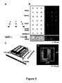
- FIG. 1 (A) SEM image of a square array of AlInGaP LED structures (50 ⁇ m by 50 ⁇ m) created by vertical, patterned etching through an epitaxial multilayer stack grown on a GaAs wafer. (B) Cross-sectional SEM view of one of these structures, showing the LED semiconductor layers (quantum wells, as well as cladding, spreading, and contact layers) on a sacrificial epilayer of AlAs. (C) Schematic illustration of a printing-based assembly method for transferring collections of LEDs (gray) released from the GaAs wafer to a target substrate (shown here as a flexible sheet).
- a pair of “breakaway” photoresist (PR) anchors at the two far corners of the device holds it above the GaAs wafer in the suspended configuration of a diving board, for ease of liftoff with a stamp.
- the white arrow points to the region of removed AlAs.
- the black arrow and white dot indicate, roughly, the region of this chip that corresponds to the image of (F).
- H Optical image of a target substrate printed with sparse arrays of devices at different spacings, derived from the chip shown in (G).
- I Large-scale collection of ILEDs (1600 devices, in a square array with pitch of 1.4 mm) printed onto a thin, flexible sheet of plastic, shown here wrapped onto a cylindrical glass substrate (main panel). The inset shows a similar collection of ILEDs (1600 devices, in a square array with pitch of 1.4 mm) printed onto a plate of glass. For these cases, relatively large ILEDs were selected for ease of viewing; devices with dimensions of (E) are invisible at this magnification.
- FIG. 2 (A) Exploded view schematic illustration of an array of ILEDs contacted by a metal mesh (bottom; n contacts) and a metal film (top; p contacts). A thin adhesive layer of PDMS facilitates printing onto the glass substrate. A photopatterned layer of epoxy on top of the devices prevents shorting of the top film to the bottom mesh. (B)Optical micrographs of an array of ILEDs (top: 25 ⁇ m by 25 ⁇ m, square geometries; bottom: characters “LED”) in their off state with frontside illumination (left) and in their on state without illumination (right).
- FIG. 1 Schematic illustration of an ILED with integrated ohmic contacts (left) and optical image of an operating device (right), showing uniform emission characteristics at all regions not directly blocked by the contacts or probe tips.
- the areas delineated by yellow and white dashed boxes correspond to the contact electrodes and the device periphery, respectively.
- the regions labeled “PT” correspond to the probe tips used to evaluate the device operation.
- D Current-voltage-emission characteristics of a representative device before undercut etching on the GaAs wafer, and after transfer printing onto a polyurethane-coated glass slide. The inset provides a histogram of the bias voltages needed to produce currents of 0.1 mA in a collection of devices.
- E Spectral characteristics of emission for a typical device on the wafer and after transfer printing.
- FIG. 3 (A) Schematic illustration of a planar scheme for interconnecting a printed array of ILEDs in a passive matrix layout. Coordinated control of voltages applied to the row and column electrodes allows operation in a passive matrix display mode. (B) Images of a flexible display that incorporates a 16 by 16 array of ILEDs in the layout shown in (A), on a sheet of plastic (PET), wrapped around the thumb of a mannequin hand (main panel; human scale; radius ⁇ 8 mm) and a cylindrical glass tube (inset; radius ⁇ 12 mm). External interface to control electronics occurs through ribbon cables bonded to column and row electrodes that emerge from the periphery of the display.
- PTT sheet of plastic
- FIG. 4 Color plots of the strain distributions (in percent) at the quantum well region and the corresponding finite element mesh used for simulation (top) and optical micrographs (bottom) of a stretchable ILED on a rubber substrate in unstrained and strained states. The bottom panels show optical micrographs in the off (top) and on (bottom) states, with and without external illumination, respectively.
- B Passive matrix, stretchable ILED display that uses a noncoplanar mesh configuration, on a rubber substrate. Here, interconnect lines between adjacent devices are supported by arc-shaped bridge structures that can deform in response to applied strain. Both the main panel and the inset images were collected with an automated camera system that combines pictures captured at different focal depths to provide a sharp, composite image.
- (C) Optical micrographs of a set of four pixels in the display shown in (B).
- the upper and lower images show optical micrographs in the off (top) and on (bottom) states, with and without external illumination, respectively.
- the multiple red spots in the case of the configuration in the left result from reflections from the interconnection bridges.
- (D) Current (I)-voltage (V) measurements on a representative ILED in the display, at different applied strains.
- FIG. 5 Schematic illustration (left) and cross sectional scanning electron microscope (SEM) image (middle) of the epitaxial semiconductor multilayer stack on a GaAs wafer.
- SEM scanning electron microscope
- FIG. 6 Schematic illustration and optical microscope/SEM images of processing steps for retrieving ILEDs from a GaAs source wafer.
- FIG. 7 Picture of the automated printing machine, with key parts labeled.
- FIG. 8 (A) Schematic illustration of retrieving and printing selected sets of ILEDs with a composite stamp. (B) Optical microscope image of the source wafer after three cycles of printing. (C) Optical microscope image of a substrate with sparsely printed ILEDs derived from the source wafer of (B), illustrating the concept of area expansion.
- FIG. 9 Schematic illustration of processing steps for ILEDs of FIG. 2A .
- TLM transmission line model
- FIG. 11 I-V curves of ILED devices with ohmic contacts with and without a passivation scheme to protect the sidewalls during undercut etching.
- B I-V curves of ILED devices (50 ⁇ 50 ⁇ m and 100 ⁇ 100 ⁇ m) with ohmic contacts and passivation scheme, before and after transfer.
- FIG. 12 (A) Schematic illustration of processing steps for fabricating electrical interconnections to complete a passive matrix array. (B) Optical microscope image of an array of ILEDs array after exposing n-GaAs by wet etching. (C) Cross sectional SEM view of an ILED after exposing n-GaAs by wet etching. (D) Optical microscope image of an array of ILEDs with electrical interconnections.
- FIG. 13 Optical images of a 16 ⁇ 16 ILED (100 ⁇ m ⁇ 100 ⁇ m with a pitch of 210 ⁇ m) display on a plastic substrate, wrapped onto the wrist (A) and finger (B, C) of mannequin. (Bottom right) a map of non-working pixels (indicated by ‘x’ symbols).
- FIG. 14 (A) Optical image of a 16 ⁇ 16 ILED (50 ⁇ m ⁇ 50 ⁇ m with a pitch of 70 ⁇ m) display on a glass substrate with ACF ribbon cable connection. (B) Optical images of the display during the operation. (Left-top) a map of non-working pixels (indicated by ‘x’ symbols).
- FIG. 15 Electrical properties of a 16 ⁇ 16 ILED (100 ⁇ m ⁇ 100 ⁇ m with a pitch of 210 ⁇ m) display on a plastic substrate.
- A Plot of voltage at 20 ⁇ A and
- C Plot of voltage at 20 ⁇ A and
- the relatively high turn-on voltages are due to the use of non-ohmic contacts.
- FIG. 16 (A, B) Optical images of a 16 ⁇ 16 ILED (100 ⁇ m ⁇ 100 ⁇ m with a pitch of 1.20 mm) display on glass substrate during operation. (C) A map of non-working pixels (indicated by ‘x’ symbols).
- FIG. 17 (A) Exploded schematic illustration of processing steps for wavy ILEDs ribbons.
- B Optical microscope image of wavy ILEDs ribbons with 50 ⁇ m and 100 ⁇ m width collected with a scanning focal technique.
- Optical microscope image of a wavy ILEDs ribbon in different strained states (from wavy to flat): (C) non-emission with illumination, (D) emission with illumination, (E) emission without illumination.
- FIG. 19 (A) Schematic illustration of processing steps for stretchable ILEDs display. (B) A map of non-working pixels (indicated by ‘x’ symbols).
- FIG. 20 Optical microscope images of a passive matrix, stretchable ILEDs display that uses a non-coplanar mesh configuration, on a flat rubber substrate.
- FIG. 21 Optical microscope and SEM images of a passive matrix, stretchable ILEDs display that uses a non-coplanar mesh configuration, on a bent/twisted rubber substrate.
- FIG. 22 (A) Schematic illustrations of a stretchable ILED on a rubber substrate in compressed (left) and stretched (right) configurations. Strain distributions in the device: (B) top surface, (C) middle surface (quantum well region), (D) bottom surface in a compressed state and (E) middle surface in a stretched state.
- FIG. 23 Strain distributions of a stretchable ILED display: (A) top surface, (B) middle surface (quantum well region), and (C) bottom surface of ILED.
- FIG. 24 Schematic illustration of procedures for printing and interconnecting microscale device components.
- the first step involves fabrication of devices (square, dark grey blocks with rectangular, gold electrodes) on a source substrate.
- An elastomeric stamp retrieves a collection of these devices by van der Waals adhesion to features of relief that contact the electrode regions.
- Scraping a conductive paste (light grey) over this structure fills the molded features to form electrical contacts to the devices and interconnects between them.
- FIG. 25 (a) Optical image of a collection of conducting features formed by molding a layer of PU on a PET substrate, and then filling the resulting trenches with silver epoxy. These results illustrate the range of feature sizes and shapes and areas that can be formed easily. (b) Cross-sectional SEM images of filled lines with depths of 20 ⁇ m and widths of 20 ⁇ m (left) and 200 ⁇ m (right). Higher aspect ratios and narrower features can be achieved with suitable modifications to the conductive material. (c) Interconnected arrays of metal pads (Cr/Au, 100/1000 nm; 500 ⁇ 500 ⁇ m; 1.5 mm pitch) with crossed, but electrically isolated conducting lines on a PET substrate.
- FIG. 26 (a) Optical image of a set of six AlInGaP light emitting diodes (LEDs; 250 ⁇ 250 ⁇ m) formed in ultrathin (2.5 ⁇ m thick) layouts and pairs of molded interconnect lines leading to each. Selective printing formed the arrays; aligned molding followed by filling with silver epoxy formed the interconnect. The top inset provides a top view optical micrograph. The three devices in the middle were connected to a power supply to cause light emission. (b) Current/voltage characteristics (non-ohmic contacts) of these LEDs.
- LEDs AlInGaP light emitting diodes
- FIG. 27 (a) Schematic illustration of a photovoltaic minimodule consisting of five monocrystalline bars of silicon with integrated contacts.
- the left and right frames show the structure before and after filling molded trenches with silver epoxy, respectively.
- the molded polymer (PU) is illustrated in tan; the silicon cells are black, with gold contacts. Filling the molded trenches with silver epoxy (light grey) yields the interconnected structure on the right.
- Each bar is 50 ⁇ m wide, 1.55 mm long and 20 ⁇ m thick, with ohmic contacts of metal (Cr/Au, 100/1000 nm; 50 ⁇ m width and 100 ⁇ m length for p contact; 50 ⁇ m width and 1.4 mm length for n contact) on p and n doped regions.
- Cr/Au 100/1000 nm
- 50 ⁇ m width and 100 ⁇ m length for p contact 50 ⁇ m width and 1.4 mm length for n contact
- FF fill factor
- FIG. 28 Epitaxial layers of GaAs LED wafer.
- FIG. 29 Processing schematics for ⁇ -GaAs LED.
- FIG. 30 A. Scanning Electron Microscopy (SEM) image of isolated GaAs LED on the host wafer. B. Scanning Electron Microscopy (SEM) image GaAs LED after heterogeneous anchors are photolithographically defined. C. Scanning Electron Microscopy (SEM) image of transfer-printed GaAs LEDs on a PET substrate. D. Optical Microscopy (OM) image of GaAs LEDs before & after transfer-printing process.
- SEM Scanning Electron Microscopy
- SEM Scanning Electron Microscopy
- OM Optical Microscopy
- FIG. 31 (A). A cartoon illustrating the printed ⁇ -GaAs LED. (B) Luminance vs. current-voltage characteristic plots.
- FIG. 32 Epitaxial layer structure of a typical GaN device on a silicon wafer.
- FIG. 33 Processing scheme of individually printable ⁇ -GaN LEDs.
- FIG. 34 Scanning electron microscopy (SEM) image of an anchor of ⁇ -GaN LED cell before (left) and after (right) KOH undercut process.
- FIG. 35 Optical image of the donor substrate after several step-and-repeat transfer-printing process has been carried out.
- FIG. 36 Step-and-repeat process on GaAs ⁇ -LEDs.
- FIG. 37 (a) Optical image (b) current-voltage characteristic and (c) emission spectrum of an individual ⁇ -GaN LED cell under operation.
- FIG. 38 SEM images of GaN LED devices before and after KOH undercut. Extended exposure to KOH causes moderate roughening of the GaN sidewalls.
- FIG. 39 Sidewall passivation scheme for printable GaN devices.
- FIG. 40 Printable GaN devices utilizing laser lift-off.
- FIG. 41 Freestanding GaN device transfer utilizing PEC etching with InGaN sacrificial layer. SEM images* of PEC etching for freestanding GaN and AlGaN layers are inserted. (*left image: E. Haberer et al. Appl. Phys. Lett. 85, 5179 (2005), right image: R. Sharma et al Appl. Phys. Lett. 87, 051107 (2005)).
- FIG. 42 Selective etching of sacrificial layer by EC (electrochemical) etching.
- FIG. 43 Selective etching of sacrificial layer (i.e. ZnO) with specific etchant (NH 4 Cl).
- FIG. 44 Optical Microscopy (OM) image of heterogeneous anchoring structures.
- FIG. 45 Various geometries of heterogeneous anchoring structures.
- FIG. 46 (A) Optical microscopy (OM) image of homogeneous anchors; (B) scanning electron microscopy (SEM) images of homogeneous anchors.
- FIG. 47 SEM images of commercially available wire-bonded LED.
- FIG. 48 (a) Schematic illustration of the cell design. (b) Process for encapsulation via back-side exposure.
- FIG. 49 (a) Scanning electron microscopy (SEM) image (b) optical microscopy (OM) image of passivated ⁇ -GaN LED using encapsulation via back-side exposure process.
- SEM Scanning electron microscopy
- OM optical microscopy
- FIG. 50 Scanned profile using a profilometer of ⁇ -GaN LED after the encapsulation via back-side exposure process.
- FIG. 51 Five ⁇ -GaN LEDs connected in series.
- FIG. 52 Two strings of five ⁇ -GaN LEDs connected in series.
- FIG. 53 Fabrication schematic for the molded interconnection.
- FIG. 54 Fabrication schematic for the molded interconnection.
- FIG. 55 (a) Optical Image of 1 GaAs LED cell. 9 GaAs LED cells with 250 ⁇ 250 ⁇ m 2 are independently metalized with a conductive silver paste. (b) Current-Voltage (I-V) characteristic of 1 GaAs LED.
- FIG. 56 Molded interconnection approach with addition of reflective layers for selective curing.
- FIG. 57 Resolution of molded interconnection approach.
- FIG. 58 GaAs vertical LED structure.
- FIG. 59 Fabrication process for the mesh interconnection approach. Also exploded view schematic illustration of an array of ILEDs contacted by a metal mesh (bottom; n contacts) and a metal film (top; p contacts) is shown.
- FIG. 60 A comparison between strings of ⁇ -LEDs connected in series and in parallel.
- FIG. 61 Optical Image of serially connected strings of ⁇ -LEDs printed on a plastic substrate.
- FIG. 62 Planar interconnection processing schematics for passive-matrix display using printed ⁇ -LEDs.
- FIG. 63 Spatially independent micro-lens array fitted to a of five ⁇ -GaN LEDs display with stretchable mechanical interconnects.
- FIG. 64 Stretchable ⁇ -LEDs.
- FIG. 65 a) Mirror-like facets increase internal reflection, but b) roughened surfaces reduces internal reflection.
- FIG. 66 Formation of pyramidal structures is performed by PEC KOH etching of a fully fabricated/undercut device in the presence of UV light.
- FIG. 67 Light Enhancement ⁇ -GaN LED with outcoupling: GaN cone structures.
- FIG. 68 GaN LED encapsulation in a polymer micro-lens increases light extraction efficiency.
- FIG. 69 Processing steps to form a micro-lens array fitted to a micro-LED display.
- FIG. 70 Processing steps to form a spatially independent micro-lens array fitted to a micro-LED display.
- FIG. 71 Schematics for optically enhancement with polymeric pattern.
- FIG. 72 Bi-directional nature of light output from the printed ⁇ -LED on transparent substrates.
- FIG. 73 Integration of reflector and thermal heat sink onto printed ⁇ -LEDs.
- FIG. 74 Multiple stacks of ⁇ -LEDs
- FIG. 75 Thermographic images at various driving conditions of AlInGaP ⁇ -LED.
- FIG. 76 Thermal management of printed ⁇ -LED on plastic substrates.
- FIG. 77 Printed ⁇ -diamond as a heat sink.
- FIG. 78 Integration of reflector & thermal heat sink onto printed ⁇ -LEDs.
- FIG. 79 Heterogeneous integration of ⁇ -LEDs with printed electronics.
- FIG. 80 Heterogeneous integration of photodiode with ⁇ -LEDs for the in situ self-calibration of the light output.
- FIG. 81 Fabrication scheme of uniform phosphor array.
- FIG. 82 Phosphors in elastomer cavities.
- FIG. 83 Laminated Phosphor-encapsulated Elastomer on top of printed and packaged LEDs.
- FIG. 84 Exemplary method of making semiconductor devices.
- FIG. 85 Exemplary method of making GaN LED devices.
- FIG. 86 Exemplary method of making GaN LED devices.
- FIG. 87 Exemplary method of making GaN LED devices.
- FIG. 88 Exemplary method of making GaN LED devices.
- FIG. 89 Illustration of a scheme for processing electronic devices on a handle substrate.
- FIG. 90 FIG. 90A
- FIG. 90B Illustration of a transfer scheme for transferring portions of a semiconductor structure to two separate handle substrates.
- FIG. 91 Illustration of a scheme for assembly of electronic devices grown on separate growth substrates on a common handle substrate.
- FIG. 92 Illustration of a scheme for assembly of electronic devices grown on separate growth substrates on a common handle substrate; FIG. 92B ) Cross sectional view of the assembled electronic devices on the handle substrate.
- FIG. 93 Illustration of a scheme for processing electronic devices on a handle substrate.
- FIG. 94 Illustration of a scheme for processing electronic devices on a handle substrate.
- Transferable or “printable” are used interchangeably and relates to materials, structures, device components and/or integrated functional devices that are capable of transfer, assembly, patterning, organizing and/or integrating onto or into substrates.
- transferring or printing refers to the direct transfer of a structure or element from one substrate to another substrate, such as from a multilayer structure to a device substrate or a device or component supported by a device substrate.
- transferable refers to a structure or element that is printed via an intermediate substrate, such as a stamp that lifts-off the structure or element and then subsequently transfers the structure or element to a device substrate or a component that is on a device substrate.
- the printing occurs without exposure of the substrate to high temperatures (i.e.
- printable or transferable materials, elements, device components and devices are capable of transfer, assembly, patterning, organizing and/or integrating onto or into substrates via solution printing or dry transfer contact printing.
- “printing” is used broadly to refer to the transfer, assembly, patterning, organizing and/or integrating onto or into substrates, such as a substrate that functions as a stamp or a substrate that is itself a target (e.g., device) substrate.
- Such a direct transfer printing provides low-cost and relatively simple repeated transfer of a functional top-layer of a multilayer structure to a device substrate. This achieves blanket transfer from, for example, a wafer to a target substrate without the need for a separate stamp substrate.
- Substrate refers to a material having a surface that is capable of supporting a component, including a device, component or an interconnect.
- An interconnect that is “bonded” to the substrate refers to a portion of the interconnect in physical contact with the substrate and unable to substantially move relative to the substrate surface to which it is bonded. Unbonded portions, in contrast, are capable of substantial movement relative to the substrate.
- the unbonded portion of an interconnect generally corresponds to that portion having a “bent configuration,” such as by strain-induced interconnect bending.
- Handle substrate and “handle substrate” interchangeably refer to a substrate on which an electronic device is assembled, processed or otherwise manipulated.
- a handle substrate is a substrate useful as a transitory substrate, for example for holding structures for subsequent transfer to another substrate, such as by transfer printing.
- a handle substrate is useful as a processing substrate, where structures present on the handle substrate undergo additional processing steps.
- “Growth substrate” refers to a substrate useful for growing material, for example via epitaxial growth.
- a growth substrate comprises the same material as is being grown.
- a growth substrate comprises material different from that being grown.
- Useful growth substrates include substrates which are lattice matched, or effectively lattice matched, to the material being grown.
- a growth substrate is a host substrate.
- “Device substrate” refers to a substrate useful for assembling device components.
- a device substrate comprises functional device components.
- a device substrate is a flexible substrate, a large area substrate, a pre-metalized substrate, a substrate pre-patterned with one or more device components, or any combination of these.
- a device substrate is a host substrate.
- surfaces as used herein is intended to be consistent with its plain meaning which refers to an outer boundary of an object.
- surfaces may be given specific names, such as “receiving surface”, “contact surface”, “external surface”.
- named surfaces can refer to their target use and/or identify subregions of a surface.
- named surfaces can refer to their orientation, for example relative to other nearby or adjacent components.
- “Functional layer” or “device layer” refers to a layer capable of incorporation into a device or device component and that provides at least partial functionality to that device or device component.
- a functional layer can include a broad range of compositions.
- a device that is a solar array can be made from a starting functional layer of III-V micro solar cells, including a functional layer that is itself made up a plurality of distinct layers as provided herein.
- release and subsequent printing of such layers provides the basis for constructing a photovoltaic device or device component.
- a functional layer for incorporation into electronics (MESFETs), LEDs, or optical systems may have a different layering configuration and/or compositions. Accordingly, the specific functional layer incorporated into the multilayer structure depends on the final device or device component in which the functional layer will be incorporated.
- Release layer (sometimes referred to as “sacrificial layer”) refers to a layer that at least partially separates one or more functional layers.
- a release layer is capable of being removed or providing other means for facilitating separation of the functional layer from other layers of the multi-layer structure, such as by a release layer that physically separates in response to a physical, thermal, chemical and/or electromagnetic stimulation, for example. Accordingly, the actual release layer composition is selected to best match the means by which separation will be provided.
- Means for separating is by any one or more separating means known in the art, such as by interface failure or by release layer sacrifice.
- a release layer may itself remain connected to a functional layer, such as a functional layer that remains attached to the remaining portion of the multilayer structure, or a functional layer that is separated from the remaining portion of the multilayer structure.
- the release layer is optionally subsequently separated and/or removed from the functional layer.
- Buffer layer refers to a layer of a device or device component which is useful for protecting other layers of the device component.
- a buffer layer protects another device layer from etching.
- a buffer layer does not impact or has a minimal impact on the function of the device.
- an etch block layer is a buffer layer.
- “Release” and “releasing” refer to at least partially separating two layers, devices or device components from one another, for example by mechanical or physical separation, or by removal of at least a portion of one layer, device or device component. In some embodiments, removal of a sacrificial layer results in the release of a layer, device or device component. In some embodiments, layers, devices or device components are released by etching away a portion of the layer, device or device component. In certain embodiments, released components remain attached to the object with they are released from by one or more anchors. In some embodiments, released components are subsequently attached to the object they are released from by one or more anchors.
- Etch and “etching” refer to a process by which a portion of a layer, device or device component is reacted away, dissolved or otherwise removed.
- an anisotropic etch or a directional etch refers to an etching process which preferentially removes material along a specific direction.
- a wet etch refers to removal of material by exposure to a solution.
- a selective etch refers to removal of a specific material or class of materials.
- a reactive ion etch or an inductively coupled plasma reactive ion etch refers to an etching method which utilizes a plasma to etch away material, for example by reaction with ions in the plasma.
- etching refers to an etching process which utilizes an applied electric potential, electric field or electric current.
- photoelectrochemical etching refers to an etching process which utilizes an applied electric potential, electric field or electric current and exposure to electromagnetic radiation.
- etch mask refers to material useful for preventing underlying material from being etched.
- a thick etch mask refers to an etch mask of a sufficient thickness that the majority of the mask remains after an etching process.
- a thick etch mask has a thickness selected over the range of 100 nm to 5 ⁇ m.
- a metal etch mask refers to an etch block layer.
- mask refers to a material which covers or otherwise blocks portions of an underlying material. Use of the term “mask” is intended to be consistent with use of the term in the art of microfabrication. In embodiments, the term “mask” refers to an etch mask, an optical mask, a deposition mask or any combination of these.
- mask region and “exposed region” respectively refer to portions of an underlying material which are blocked and unblocked by a mask.
- Epilayer refers to a layer grown via epitaxial growth.
- patterning is used herein as in the art of microfabrication to broadly refer to a process by which portions of a layer, device or device component are selectively removed or deposited to create a specified structure.
- “Supported by a substrate” refers to a structure that is present at least partially on a substrate surface or present at least partially on one or more intermediate structures positioned between the structure and the substrate surface.
- the term “supported by a substrate” may also refer to structures partially or fully embedded in a substrate.
- Printable electronic device or “printable electronic device component” refer to devices and structures that are configured for assembly and/or integration onto substrate surfaces, for example by using dry transfer contact printing and/or solution printing methods.
- a printable electronic device component is a printable semiconductor element.
- printable semiconductor elements are unitary single crystalline, polycrystalline or microcrystalline inorganic semiconductor structures.
- printable semiconductor elements are connected to a substrate, such as a mother wafer, via one or more bridge or anchor elements.
- a unitary structure is a monolithic element having features that are mechanically connected.
- Semiconductor elements of various embodiments may be undoped or doped, may have a selected spatial distribution of dopants and may be doped with a plurality of different dopant materials, including p- and n-type dopants.
- Certain microstructured printable semiconductor elements include those having at least one cross sectional dimension greater than or equal to about 1 micron and nanostructured printable semiconductor elements having at least one cross sectional dimension less than or equal to about 1 micron.
- a printable semiconductor element comprises a composite heterogeneous structure having a semiconductor operationally connected to or otherwise integrated with at least one additional device component or structure, such as a conducting layer, dielectric layer, electrode, additional semiconductor structure or any combination of these.
- the printable semiconductor element(s) comprises a semiconductor structure integrated with at least one additional structure selected from the group consisting of: another semiconductor structure; a dielectric structure; conductive structure, and an optical structure (e.g., optical coatings, reflectors, windows, optical filter, collecting, diffusing or concentration optic etc.).
- a printable semiconductor element comprises a semiconductor structure integrated with at least one electronic device component selected from the group consisting of: an electrode, a dielectric layer, an optical coating, a metal contact pad a semiconductor channel.
- printable semiconductor elements comprise stretchable semiconductor elements, bendable semiconductor elements and/or heterogeneous semiconductor elements (e.g., semiconductor structures integrated with one or more additional materials such as dielectrics, other semiconductors, conductors, ceramics etc.).
- Printable semiconductor elements include printable semiconductor devices and components thereof, including but not limited to printable LEDs, lasers, solar cells, p-n junctions, photovoltaics, photodiodes, diodes, transistors, integrated circuits, and sensors.
- Electrode component refers to a printable semiconductor or electrical device. Exemplary electronic device component embodiments are configured for performing a function, for example emitting electromagnetic radiation or converting electromagnetic radiation into electrical energy. In specific embodiments, multiple electronic device components are electrically interconnected and perform a more complex task or function than the individual device components perform alone.
- Useful electronic device components include, but are not limited to P-N junctions, thin film transistors, single junction solar cells, multi-junction solar cells, photodiodes, light emitting diodes, lasers, CMOS devices, MOSFET devices, MESFET devices, photovoltaic cells, microelectricalmechanical devices and HEMT devices.
- “Vertical type LED” refers to a light emitting diode device in which the functional components or layers of the device are arranged in a stacked configuration and the electrical contacts are made at the top and bottom of the stack.
- Solution printing is intended to refer to processes whereby one or more structures, such as transferable or printable elements, are dispersed into a carrier medium and delivered in a concerted manner to selected regions of a substrate surface.
- delivery of structures to selected regions of a substrate surface is achieved by methods that are independent of the morphology and/or physical characteristics of the substrate surface undergoing patterning.
- Solution printing methods include, but are not limited to, ink jet printing, thermal transfer printing, and capillary action printing.
- Contact printing refers broadly to a dry transfer contact printing method such as with a stamp that facilitates transfer of features from a stamp surface to a substrate surface.
- the stamp is an elastomeric stamp.
- the transfer can be directly to a target (e.g., device) substrate or host substrate.
- the following references relate to self assembly techniques which may be used in methods of the present invention to transfer, assembly and interconnect transferable semiconductor elements via contact printing and/or solution printing techniques and are incorporated by reference in their entireties herein: (1) “Guided molecular self-assembly: a review of recent efforts”, Jiyun C Huie Smart Mater. Struct.
- Useful contact printing methods for assembling, organizing and/or integrating transferable elements include dry transfer contact printing, microcontact or nanocontact printing, microtransfer or nanotransfer printing and self assembly assisted printing.
- Use of contact printing is beneficial because it allows assembly and integration of a plurality of transferable semiconductor in selected orientations and positions relative to each other.
- Contact printing also enables effective transfer, assembly and integration of diverse classes of materials and structures, including semiconductors (e.g., inorganic semiconductors, single crystalline semiconductors, organic semiconductors, carbon nanomaterials etc.), dielectrics, and conductors.
- Contact printing methods optionally provide high precision registered transfer and assembly of transferable semiconductor elements in preselected positions and spatial orientations relative to one or more device components prepatterned on a device substrate.
- Contact printing is also compatible with a wide range of substrate types, including conventional rigid or semi-rigid substrates such as glasses, ceramics and metals, and substrates having physical and mechanical properties attractive for specific applications, such as flexible substrates, bendable substrates, shapeable substrates, conformable substrates and/or stretchable substrates.
- Contact printing assembly of transferable structures is compatible, for example, with low temperature processing (e.g., less than or equal to 298K). This attribute allows the present optical systems to be implemented using a range of substrate materials including those that decompose or degrade at high temperatures, such as polymer and plastic substrates.
- Contact printing transfer, assembly and integration of device elements is also beneficial because it can be implemented via low cost and high-throughput printing techniques and systems, such as roll-to-roll printing and flexographic printing methods and systems.
- Stretchable refers to the ability of a material, structure, device or device component to be strained without undergoing fracture.
- a stretchable material, structure, device or device component may undergo strain larger than about 0.5% without fracturing, preferably for some applications strain larger than about 1% without fracturing and more preferably for some applications strain larger than about 3% without fracturing.
- a flexible material, structure, device or device component may be deformed into a curved shape without introducing strain larger than or equal to about 5%, preferably for some applications larger than or equal to about 1%, and more preferably for some applications larger than or equal to about 0.5%.
- semiconductor refers to any material that is an insulator at very low temperatures, but which has an appreciable electrical conductivity at a temperatures of about 300 Kelvin. In the present description, use of the term semiconductor is intended to be consistent with use of this term in the art of microelectronics and electrical devices.
- Useful semiconductors include element semiconductors, such as silicon, germanium and diamond, and compound semiconductors, such as group IV compound semiconductors such as SiC and SiGe, group III-V semiconductors such as AlSb, AlAs, Aln, AlP, BN, GaSb, GaAs, GaN, GaP, InSb, InAs, InN, and InP, group III-V ternary semiconductors alloys such as AlxGal-xAs, group II-VI semiconductors such as CsSe, CdS, CdTe, ZnO, ZnSe, ZnS, and ZnTe, group I-VII semiconductors CuCI, group IV-VI semiconductors such as PbS, PbTe and SnS, layer semiconductors such as PbI 2 , MoS 2 and GaSe, oxide semiconductors such as CuO and Cu 2 O.
- group IV compound semiconductors such as SiC and SiGe
- group III-V semiconductors such as AlSb, AlAs, Aln,
- semiconductor includes intrinsic semiconductors and extrinsic semiconductors that are doped with one or more selected materials, including semiconductor having p-type doping materials (also known as P-type or p-doped semiconductor) and n-type doping materials (also known as N-type or n-doped semiconductor), to provide beneficial electrical properties useful for a given application or device.
- semiconductor includes composite materials comprising a mixture of semiconductors and/or dopants.
- Useful specific semiconductor materials include, but are not limited to, Si, Ge, SiC, AlP, AlAs, AlSb, GaN, GaP, GaAs, GaSb, InP, InAs, GaSb, InP, InAs, InSb, ZnO, ZnSe, ZnTe, CdS, CdSe, ZnSe, ZnTe, CdS, CdSe, CdTe, HgS, PbS, PbSe, PbTe, AlGaAs, AlInAs, AlInP, GaAsP, GaInAs, GaInP, AlGaAsSb, AlGaInP, and GaInAsP.
- Porous silicon semiconductor materials are useful in the field of sensors and light emitting materials, such as light emitting diodes (LEDs) and solid state lasers.
- Impurities of semiconductor materials are atoms, elements, ions and/or molecules other than the semiconductor material(s) themselves or any dopants provided to the semiconductor material. Impurities are undesirable materials present in semiconductor materials which may negatively impact the electrical properties of semiconductor materials, and include but are not limited to oxygen, carbon, and metals including heavy metals. Heavy metal impurities include, but are not limited to, the group of elements between copper and lead on the periodic table, calcium, sodium, and all ions, compounds and/or complexes thereof.
- the term “orientation” refers to a specific plane of a crystal structure, for example a semiconductor crystal.
- the term “direction” refers to a specific axis, or equivalent axes, of a crystal structure.
- use of the terms orientation and direction with a specific numeric indicator is intended to be consistent with use in the fields of crystallography and microfabrication.
- Quantum well refers to an active layer of a light emitting diode device.
- a quantum well is a layer of an LED device having a relatively narrow bandgap, surrounded on two sides by layers having a relatively wider bandgap.
- Barrier layer refers to a layer of a light emitting diode device which is positioned adjacent to a quantum well layer and has a larger bandgap than the quantum well material.
- a quantum well layer is sandwiched between two barrier layers. In another embodiment, multiple quantum well layers are sandwiched between multiple barrier layers.
- Contact layer refers to a layer of a light emitting diode device, for example used to make electrical contact with external circuit components, such as electrical interconnects.
- Film layer refers to a layer of a light emitting diode device, for example useful for providing voltage or current from a contact layer across the area of a light emitting diode device.
- Fusion layer refers to a layer of a light emitting diode device, for example a layer surrounding the barrier layer and quantum well layer.
- Good electronic performance and “high performance” are used synonymously in the present description and refer to devices and device components have electronic characteristics, such as field effect mobilities, threshold voltages and on-off ratios, providing a desired functionality, such as electronic signal switching and/or amplification.
- Exemplary printable elements exhibiting good electronic performance may have intrinsic field effect mobilities greater than or equal 100 cm 2 V ⁇ 1 s ⁇ 1 , and for some applications, greater than or equal to about 300 cm 2 V ⁇ 1 s ⁇ 1 .
- Exemplary transistors exhibiting good electronic performance may have device field effect mobilities great than or equal to about 100 cm 2 V ⁇ 1 s ⁇ 1 , for some applications, greater than or equal to about 300 cm 2 V ⁇ 1 s ⁇ 1 , and for other applications, greater than or equal to about 800 cm 2 V ⁇ 1 s ⁇ 1 .
- Exemplary transistors of exhibiting good electronic performance may have threshold voltages less than about 5 volts and/or on-off ratios greater than about 1 ⁇ 10 4 .
- Plastic refers to any synthetic or naturally occurring material or combination of materials that can be molded or shaped, generally when heated, and hardened into a desired shape.
- Useful plastics include, but are not limited to, polymers, resins and cellulose derivatives.
- the term plastic is intended to include composite plastic materials comprising one or more plastics with one or more additives, such as structural enhancers, fillers, fibers, plasticizers, stabilizers or additives which may provide desired chemical or physical properties.
- Prepolymer refers to a material which is a polymer precursor and/or a material which, when cured, is a polymer.
- a “liquid prepolymer” refers to a prepolymer which exhibits one or more properties of a liquid, for example flow properties. Specific prepolymers include, but are not limited to, photocurable polymers, thermally curable polymers and photocurable polyurethanes.
- “Curing” refers to a process by which a material is transformed such that the transformed material exhibits one or more properties different from the original, non-transformed material.
- a curing process allows a material to become solid or rigid.
- curing transforms a prepolymer material into a polymer material.
- Useful curing processes include, but are not limited to, exposure to electromagnetic radiation (photocuring processes), for example exposure to electromagnetic radiation of a specific wavelength or wavelength range (e.g., ultraviolet or infrared electromagnetic radiation); thermal curing processes, for example heating to a specific temperature or within a specific temperature range (e.g., 150° C.
- one embodiment for curing a silver epoxy comprises heating the silver epoxy to 150° C. for a duration of 5 minutes.
- Polymer refers to a molecule comprising a plurality of repeating chemical groups, typically referred to as monomers. Polymers are often characterized by high molecular masses. Useful polymers include organic polymers and inorganic polymers, both of which may be in amorphous, semi-amorphous, crystalline or partially crystalline states. Polymers may comprise monomers having the same chemical composition or may comprise a plurality of monomers having different chemical compositions, such as a copolymer. Cross linked polymers having linked monomer chains are also useful for some embodiments. Useful polymers include, but are not limited to, plastics, elastomers, thermoplastic elastomers, elastoplastics, thermostats, thermoplastics and acrylates.
- Exemplary polymers include, but are not limited to, acetal polymers, biodegradable polymers, cellulosic polymers, fluoropolymers, nylons, polyacrylonitrile polymers, polyamide-imide polymers, polyimides, polyarylates, polybenzimidazole, polybutylene, polycarbonate, polyesters, polyetherimide, polyethylene, polyethylene copolymers and modified polyethylenes, polyketones, poly(methyl methacrylate, polymethylpentene, polyphenylene oxides and polyphenylene sulfides, polyphthalamide, polypropylene, polyurethanes, styrenic resins, sulfone based resins, vinyl-based resins or any combinations of these.
- Elastomer refers to a polymeric material which can be stretched or deformed and return to its original shape without substantial permanent deformation. Elastomers commonly undergo substantially elastic deformations. Useful elastomers may comprise polymers, copolymers, composite materials or mixtures of polymers and copolymers. An elastomeric layer refers to a layer comprising at least one elastomer. Elastomeric layers may also include dopants and other non-elastomeric materials.
- Useful elastomer embodiments include, but are not limited to, thermoplastic elastomers, styrenic materials, olefenic materials, polyolefin, polyurethane thermoplastic elastomers, polyamides, synthetic rubbers, PDMS, polybutadiene, polyisobutylene, poly(styrene-butadiene-styrene), polyurethanes, polychloroprene and silicones.
- Transfer device or “transfer substrate” refers to a substrate, device or device component capable of and/or configured for receiving and/or relocating an element or array of elements, such as printable elements.
- Useful transfer devices include conformal transfer devices, such as devices having one or more contact surfaces capable of establishing conformal contact with elements undergoing transfer.
- An elastomeric stamp and/or transfer device is useful with a variety of the methods and devices described herein.
- Useful elastomeric transfer devices include, but are not limited to, elastomeric stamps, composite elastomeric stamps, an elastomeric layer, a plurality of elastomeric layers and an elastomeric layer coupled to a substrate such as a glass, ceramic, metal or polymer substrate.
- Target substrate is used broadly to refer to the desired final substrate that will support the transferred structure.
- the target substrate is a device substrate.
- the target substrate is a device component or element that is itself supported by a substrate.
- “Large area” refers to an area, such as the area of a receiving surface of a substrate used for device fabrication, greater than or equal to about 36 square inches.
- Pre-metalized refers to a structure which includes metallic layers, components or features.
- Pre-patterned refers to a structure which includes one or more devices, components or relief features.
- Optical communication refers to a configuration of two or more elements wherein one or more beams of electromagnetic radiation are capable of propagating from one element to the other element. Elements in optical communication may be in direct optical communication or indirect optical communication. “Direct optical communication” refers to a configuration of two or more elements wherein one or more beams of electromagnetic radiation propagate directly from a first device element to another without use of optical components for steering and/or combining the beams. “Indirect optical communication” refers to a configuration of two or more elements wherein one or more beams of electromagnetic radiation propagate between two elements via one or more device components including, but not limited to, wave guides, fiber optic elements, reflectors, filters, prisms, lenses, gratings and any combination of these device components.
- Electrode contact and “electrical communication” refers to the arrangement of one or more objects such that an electric current efficiently flows from one object to another. For example, in some embodiments, two objects having an electrical resistance between them less than 100 ⁇ are considered in electrical communication with one another.
- An electrical contact can also refer to a component of a device or object used for establishing electrical communication with external devices or circuits, for example an electrical interconnection.
- Electrode resistivity refers to a property of a material characteristic of the resistance to flow of electrons through the material.
- Electrode interconnection and “electrical interconnect” refers to a component of an electrical device used for providing electrical communication between two or more device components.
- an electrical interconnect is used to provide electrical communication between two device components spatially separated from one another, for example spatially separated by a distance greater than 50 nm, for some applications greater than 100 nm, for other applications greater than 1 ⁇ m, and for yet other applications greater than 50 ⁇ m.
- Electrode contact refers to a component of an electronic device or device component to which an electrical interconnect attaches or provides electrical communication to or from.
- Embed refers to a process by which one object or device is buried, conformally surrounded or otherwise placed or positioned within or below the surface another object, layer or material. “Encapsulate” refers to the orientation of one structure such that it is entirely surrounded by one or more other structures. “Partially encapsulated” refers to the orientation of one structure such that it is partially surrounded by one or more other structures.
- Replicate refers to a process by which one or more relief features are transferred and/or recreated during casting, molding, embedding, or embossing processes. Replicated features generally resemble the features they originate from except that the replicated features represent the negative of the original features; that is where the original features are raised features, the replicated features are recessed features and where the original features are recessed features, the replicated features are raised features.
- Relief feature refers to portions of an object or layer exhibiting differences in elevation and slope between the higher and lower parts of the surface of a given area or portion of the object or layer. “Raised features” refer to relief features which extend above the surface or average surface level of an object or layer or relief features which have elevations higher than other portions of the surface of an object or layer. “Recessed feature” refer to relief features which extend below the surface or average surface level of an object or layer or relief features which have elevations lower than other portions of the surface of an object or layer.
- Conformal contact refers to contact established between surfaces, coated surfaces, and/or surfaces having materials deposited thereon which may be useful for transferring, assembling, organizing and integrating structures (such as printable elements) on a substrate surface.
- conformal contact involves a macroscopic adaptation of one or more contact surfaces of a conformal transfer device to the overall shape of a substrate surface or the surface of an object such as a printable element.
- conformal contact involves a microscopic adaptation of one or more contact surfaces of a conformal transfer device to a substrate surface leading to an intimate contact without voids. The term conformal contact is intended to be consistent with use of this term in the art of soft lithography.
- Conformal contact may be established between one or more bare contact surfaces of a conformal transfer device and a substrate surface.
- conformal contact may be established between one or more coated contact surfaces, for example contact surfaces having a transfer material, printable element, device component, and/or device deposited thereon, of a conformal transfer device and a substrate surface.
- conformal contact may be established between one or more bare or coated contact surfaces of a conformal transfer device and a substrate surface coated with a material such as a transfer material, solid photoresist layer, prepolymer layer, liquid, thin film or fluid.
- Bind and bound refers to the physical attachment of one object to another. Bind and bound can also refer the retention of one object on another. In one embodiment an object can bind to another by establishing a force between the objects. In some embodiments, objects are bound to one another through use of an adhesion layer. In one embodiment, an adhesion layer refers to a layer used for establishing a bonding force between two objects.
- “Placement accuracy” refers to the ability of a transfer method or device to transfer a printable element, to a selected position, either relative to the position of other device components, such as electrodes, or relative to a selected region of a receiving surface. “Good placement accuracy” refers to methods and devices capable of transferring a printable element to a selected position relative to another device or device component or relative to a selected region of a receiving surface with spatial deviations from the absolutely correct position less than or equal to 50 microns, more preferably less than or equal to 20 microns for some applications and even more preferably less than or equal to 5 microns for some applications. Methods and devices described herein include those comprising at least one printable element transferred with good placement accuracy.
- “Fidelity” refers to a measure of how well a selected pattern of elements, such as a pattern of printable elements, is transferred to a receiving surface of a substrate.
- Good fidelity refers to transfer of a selected pattern of elements wherein the relative positions and orientations of individual elements are preserved during transfer, for example wherein spatial deviations of individual elements from their positions in the selected pattern are less than or equal to 500 nanometers, more preferably less than or equal to 100 nanometers.
- Undercut refers to a structural configuration wherein the bottom surfaces of an element, such as a printable element, bridge element and/or anchor element, are at least partially detached from or not fixed to another structure, such as a mother wafer or bulk material.
- Entirely undercut refers to a refers to a structural configuration wherein the bottom surfaces of an element, such as printable element, bridge element and/or anchor element, is completely detached from another structure, such as a mother wafer or bulk material.
- Undercut structures may be partially or entirely free standing structures. Undercut structures may be partially or fully supported by another structure, such as a mother wafer or bulk material, that they are detached from. Undercut structures may be attached, affixed and/or connected to another structure, such as a wafer or other bulk material, at surfaces other than the bottom surfaces.
- Anchor refers to a structure useful for connecting or tethering one device or device component to another. “Anchoring” refers to a process resulting in the connection or tethering of one device or device component to another.
- “Homogeneous anchoring” refers to an anchor that is an integral part of the functional layer.
- methods of making transferable elements by homogenous anchoring systems is optionally by providing a wafer, depositing a sacrificial layer on at least a portion of a wafer surface, defining semiconductor elements by any means known in the art, and defining anchor regions.
- the anchor regions correspond to specific regions of the semiconductor element.
- the anchor regions can correspond to a geometrical configuration of a semiconductor layer, e.g., anchors defined by relatively large surface areas and are connected to transferable elements by bridge or tether elements. Such geometry provides a means for facilitating lift-off of specific non-anchored regions for either single-layer or multi-layer embodiments.
- anchors correspond to semiconductor regions that are attached or connected to the underlying wafer. Removing the sacrificial layer provides a means for removing or transferring semiconductor elements while the portion of semiconductor physically connected to the underlying wafer remains.
- Heterogeneous anchoring refers to an anchor that is not an integral part of the functional layer, such as anchors that are made of a different material than the semiconductor layer or is made of the same material, but that is defined after the transferable semiconductor elements are placed in the system.
- One advantage of heterogeneous anchoring compared to homogeneous anchoring relates to better transfer defining strategies and further improvement to the effective useable wafer footprint.
- a wafer is provided, the wafer is coated with a sacrificial layer, semiconductor elements are defined, and heterogeneous anchor elements are deposited that anchor semiconductor regions.
- the anchor is a resist material, such as a photoresist or SiN (silicon nitride), or other material that has a degree of rigidity capable of anchoring and resisting a lift-off force that is not similarly resisted by non-anchored regions.
- the anchor may span from the top-most semiconductor layer through underlying layers to the underlying wafer substrate. Removal of sacrificial layer provides a means for removing unanchored regions while the anchored regions remain connected to the wafer, such as by contact transfer, for example.
- the anchor provides anchoring of a top layer to an underlying semiconductor layer.
- the anchoring system is for single-layer semiconductor layer systems.
- Carrier film refers to a material that facilitates separation of layers.
- the carrier film may be a layer of material, such as a metal or metal-containing material positioned adjacent to a layer that is desired to be removed.
- the carrier film may be a composite of materials, including incorporated or attached to a polymeric material or photoresist material, wherein a lift-off force applied to the material provides release of the composite of materials from the underlying layer (such as a functional layer, for example).
- Dielectric and dielectric material are used synonymously in the present description and refer to a substance that is highly resistant to flow of electric current.
- Useful dielectric materials include, but are not limited to, SiO 2 , Ta 2 O 5 , TiO 2 , ZrO 2 , Y 2 O 3 , Si 3 N 4 , STO, BST, PLZT, PMN, and PZT.
- Device field effect mobility refers to the field effect mobility of an electronic device, such as a transistor, as computed using output current data corresponding to the electronic device.
- Frill factor refers to the percentage of the area between two elements, such as between two electrodes, that is occupied by a material, element and/or device component.
- two electrodes are provided in electrical contact with one or more printable semiconductor elements that provide a fill factor between first and second electrodes greater than or equal to 20%, preferably greater than or equal to 50% for some applications and more preferably greater than or equal to 80% for some applications.
- Collecting and “concentrating”, as applied to optics and optical components refers to the characteristic of optical components and device components that collect light from a first area, in some cases a large area, and optionally direct that light to another area, in some cases a relatively smaller area.
- collecting and concentrating optical components and/or optical components are useful for light detection or power harvesting by printed solar cells or photodiodes.
- Conductive material refers to a substance or compound possessing an electrical resistivity which is typical of or equivalent to that of a metal, for example copper, silver or aluminum.
- the electrical resistivity of a conductive material is selected over the range of 1 ⁇ 10 ⁇ 1 ° to 1 ⁇ 10 ⁇ 2 ⁇ cm.
- use of the term conductive material is intended to be consistent with use of this term in the art of electronic devices and electric circuits.
- conductive materials are useful as electrical interconnections and/or for providing electrical communication between two devices.
- a “conductive paste” refers to a conductive material comprising a mixture which is generally soft and malleable.
- cured conductive pastes lose their soft and malleable nature and generally exhibit properties of a solid or a monolithic body.
- Exemplary conductive pastes comprise metal micro- and/or nano-particles.
- Silver epoxy refers to a conductive paste comprising micro- and/or nano particles including metallic silver (Ag) and which, when cured, exhibits a low electrical resistivity, for example an electrical resistivity lower than 1 ⁇ 10 ⁇ 5 ⁇ cm or selected over the range of 1 ⁇ 10 ⁇ 10 to 1 ⁇ 10 ⁇ 5 ⁇ cm.
- “Fill” and “filling” refer to a process of depositing a material into a recessed feature.
- a recessed region is filled by scraping material across and into the recessed feature.
- a filling tool generally refers to a device for moving material into a recessed feature.
- a filling tool refers to a device for scraping material across and/or into a recessed region.
- a filling tool comprises a layer or solid body of PDMS.
- a filling process is conceptually similar to a screen printing process where a material is scraped across a recessed feature by a tool or device having dimensions larger than the recessed feature, thereby at least partially filling the recessed feature with the material.
- aligned off center refers to a process by which the centers of two objects or two areas are arranged such that the two centers are not coincident with respect to one or more spatial dimensions.
- aligned off center refers to alignment of the center of two objects such that the centers of the objects are spatially separated by a distance greater than 50 nm, for some applications greater than 100 nm, for other applications greater than 1 ⁇ m, and for yet other applications greater than 50 ⁇ m.
- Young's modulus refers to a mechanical property of a material, device or layer which refers to the ratio of stress to strain for a given substance. Young's modulus may be provided by the expression;
- E Young's modulus
- L 0 the equilibrium length
- ⁇ L the length change under the applied stress
- F the force applied
- A the area over which the force is applied.
- Young's modulus may also be expressed in terms of Lame constants via the equation:
- High Young's modulus (or “high modulus”) and low Young's modulus (or “low modulus”) are relative descriptors of the magnitude of Young's modulus in a give material, layer or device.
- a High Young's modulus is larger than a low Young's modulus, about 10 times larger for some applications, more preferably about 100 times larger for other applications and even more preferably about 1000 times larger for yet other applications.
- Described herein are printable structures and methods for making, assembling and arranging electronic devices.
- a number of the methods described herein are useful for assembling electronic devices where one or more device components are embedded in a polymer which is patterned during the embedding process with trenches for electrical interconnects between device components.
- Some methods described herein are useful for assembling electronic devices by printing methods, such as by dry transfer contact printing methods.
- FIG. 24 illustrates an exemplary embodiment of a method for assembling an electronic device.
- the electronic device components are printable device components including electrode contacts 2402 .
- a transfer substrate is also provided with a patterned surface 2403 .
- the patterned surface contains features for contacting and retrieving the device components onto the transfer substrate.
- the patterned surface also contains raised features 2404 which represent the orientation and configuration of electrical interconnects to be fabricated between some of the electronic device components.
- the patterned transfer substrate is brought into contact with the electronic device components 2401 , where they are retrieved onto the transfer substrate.
- a host substrate having a prepolymer layer 2405 thereon is then provided to receive the electronic device components 2401 .
- the patterned transfer substrate 2403 having the electronic device components 2401 thereon is brought into contact with the prepolymer layer 2405 .
- the electronic device components 2401 are embedded into the prepolymer layer 2405 and, during this step, the patterned surface of the transfer substrate 2403 is also brought into contact with the prepolymer layer 2405 .
- the raised features 2404 of the patterned surface are also embedded into the prepolymer layer 2405 , at least partially, after which the prepolymer layer 2405 is cured into a hardened polymer layer 2406 .
- the embedded electronic device components are fixed into place within the polymer 2406 , and the raised features of the patterned transfer surface are replicated as recessed features 2407 in the polymer layer 2406 .
- the patterned transfer substrate 2403 and the polymer layer 2406 are separated and the electronic device components 2401 are retained in the polymer layer 2406 .
- the polymer layer includes a number of recessed features 2407 .
- the recessed features 2407 are filled with a conducting material to form electrical interconnects 2408 between the electronic device components 2401 .
- a line of silver epoxy conductive paste is provided on the surface of the polymer.
- the silver epoxy is then filled into the recessed features by dragging a filling tool across the surface of the polymer.
- the filling tool is dragged across the surface of the polymer multiple times and in multiple directions to fill the recessed features. If necessary or desired, additional silver epoxy can be provided on the surface and the dragging steps repeated to ensure that the recessed features are filled to the desired level.
- the conductive paste is cured to form rigid electrical interconnections.
- LEDs microscale inorganic light-emitting diodes
- the LEDs use specialized epitaxial semiconductor layers that allow delineation and release of large collections of ultrathin devices. Diverse shapes are possible, with dimensions from micrometers to millimeters, in either flat or “wavy” configurations.
- Printing-based assembly methods can deposit these devices on substrates of glass, plastic, or rubber, in arbitrary spatial layouts and over areas that can be much larger than those of the growth wafer.
- the thin geometries of these LEDs enable them to be interconnected by conventional planar processing techniques. Displays, lighting elements, and related systems formed in this manner can offer interesting mechanical and optical properties.
- Display devices represent ubiquitous, central components of nearly all consumer electronics technologies.
- Organic light emitting diodes OLEDs
- ILEDs Inorganic light emitting diodes
- These displays exist, however, only in ultralarge-area, low-resolution formats (square meters; billboard displays), limited by processing and assembly procedures that do not scale effectively to small ( ⁇ ⁇ 200 ⁇ m by 200 ⁇ m), thin ( ⁇ ⁇ 200 ⁇ m) light emitters or to dense, high-pixel count arrays.
- ILEDs i.e., wafer sawing, serial pick-and-place, wire bonding, and packaging on a device-by-device basis
- displays i.e., robotic assembly into tiles followed by interconnection using large quantities of bulk wiring
- Examples include not only ILED displays for desktop monitors, home theater systems, and instrumentation gauging, but also, when implemented in flexible or stretchable forms, wearable health monitors or diagnostics and biomedical imaging devices. In microscale sizes, such ILEDs can also yield semitransparent displays, with the potential for bidirectional emission characteristics, for vehicle navigation, heads-up displays, and related uses.
- This example provides routes to create ultrathin, ultrasmall ILEDs in flat or “wavy” geometries and to assemble them into addressable arrays using scalable processing techniques, on substrates ranging from glass to plastic and rubber.
- the strategy includes four components: (i) epitaxial semiconductor multilayers designed for lateral delineation and release from a source wafer to yield isolated arrays of ILEDs, each of which remains tethered to the wafer by polymeric “breakaway” anchor structures; (ii) printing techniques for manipulating the resulting ILEDs in schemes that enable formation of large-scale arrays on foreign substrates and in arbitrary spatial layouts; (iii) planar processing methods for establishing electrical interconnects to the devices, in direct or matrix addressable configurations; and (iv) integration strategies capable of yielding ILED displays in flexible or stretchable formats and with conventional, semitransparent, or bidirectional emission characteristics. Certain aspects build on previously reported procedures for etching and manipulating epitaxial semiconductor layers and for fabricating flexible and stretchable electronics.
- FIG. 1 presents aspects of the first two of the components.
- the epitaxial semiconductor layers include AlInGaP quantum well structures (6-nm-thick In 0.56 Ga 0.44 P wells, with 6-nm-thick barriers of Al 0.25 Ga 0.25 In 0.5 P on top and bottom), cladding films (200-nm thick layers of In 0.5 Al 0.5 P:Zn and In 0.5 Al 0.5 P:Si for the p and n sides, respectively), spreaders (800-nm-thick layers of Al 0.45 Ga 0.55 As:C and Al 0.45 Ga 0.55 As:Si for the p and n sides, respectively), and contacts (5-nm-thick layer of GaAs:C and 500-nm-thick layer of GaAs:Si for the p and n sides, respectively), for a total thickness of ⁇ 2.523 ⁇ m all grown on AlAs (1500-nm-thick layer of Al 0.96 Ga 0.04 As:Si) on a GaAs substrate ( FIG.
- the AlAs can be removed by etching with hydrofluoric (HF) acid, in procedures that do not alter the overlying layers or the underlying substrate.
- the process for defining the ILEDs first involves forming a pattern of vertical trenches through the epitaxial layers by inductively coupled plasma reactive ion etching through a mask of SiO 2 defined photolithographically ( FIG. 6 ). This step determines the lateral geometries of the devices ( FIG. 5 ).
- FIGS. 1 , A and B shows top and cross-sectional scanning electron microscope (SEM) images collected after this etching process for a representative case, where the device islands in FIG. 1 are 50 ⁇ m by 50 ⁇ m.
- FIGS. 7 Creating a pattern of photoresist posts (i.e., “breakaway” anchors) located at two of the four corners of each island, followed by immersion in concentrated HF, leads to the undercut release of an organized array of ILEDs.
- the anchors hold the devices in their lithographically defined locations to prevent liftoff into the etching bath, even after complete undercut ( FIG. 6 ).
- an automated printing tool FIG. 7 ) brings a soft elastomeric stamp with features of relief embossed onto its surface into aligned contact with a selected set of these ILEDs. Peeling the stamp away fractures the photoresist anchors and leaves the devices adhered via Van der Waals interactions to the raised regions of relief.
- FIGS. 7 brings a soft elastomeric stamp with features of relief embossed onto its surface into aligned contact with a selected set of these ILEDs. Peeling the stamp away fractures the photoresist anchors and leaves the devices adhered via Van der Waals interactions to the raised regions of relief
- FIG. 1 shows schematic illustrations of the printing process and an SEM image of an array of anchored ILEDs on the source wafer after one cycle of printing ( FIG. 8 ).
- the white arrows in FIG. 1D highlight the collection of ILEDs removed by this process, corresponding to every third device along the two orthogonal axes of the square array.
- FIG. 1E provides an SEM image of these devices printed onto a glass substrate.
- the engineering design of the breakaway anchors is such that they are sufficiently robust to hold the ILEDs in their lithographically defined locations during the undercut etching and drying processes but sufficiently fragile to enable high-yield liftoff during printing.
- Three design aspects are the use of (i) a pair of anchors on the same side of each ILED, to yield, after undercut, suspended, “diving board” layouts ( FIG. 1F ) that enable transfer of torques large enough to fracture the photoresist upon peel-back of the stamp; (ii) stamps with relief structures that are slightly smaller than the ILEDs and are offset from the centers of the devices to maximize these torques and also to minimize overlap with the anchors; and (iii) photoresist structures that fracture more readily than the semiconductor material.
- This type of anchoring scheme (i.e., heterogeneous anchoring) is much more efficient in active materials utilization and versatile in design choices than corresponding methods demonstrated previously for transistors and solar cells, where peripheral parts of the devices themselves serve as the anchors (i.e., homogeneous anchoring).
- Conventional wafer dicing and pick-and-place methods are not suitable for devices with the thicknesses and dimensions in the range reported here, due to challenges associated with wafer utilization, device fragility, and size. Such techniques also lack the high-throughput, parallel operation of the type of printing methods described above.
- FIG. 1G shows a micrograph of a densely packed array of anchored, undercut ILEDs on a source wafer.
- FIG. 1H shows sparse assemblies of these devices formed by printing in a step-and-repeat fashion from this wafer to a glass substrate, coated with a thin ( ⁇ 10 mm) layer of poly(dimethylsiloxane) (PDMS) to promote dry, conformal adhesion.
- PDMS poly(dimethylsiloxane)
- 1I presents images of collections of ILEDs printed onto a thin sheet of polyethylene terephthalate (PET, 50 ⁇ m thick), shown as wrapped around a cylindrical glass support (1600 devices, in a square array with pitch of 1.4 mm; radius of cylinder ⁇ 25 mm) and onto a plate of glass (inset; 1600 devices, in a square array with pitch of 1.4 mm).
- PET polyethylene terephthalate
- the devices were selected to have sizes (i.e., 250 ⁇ m by 250 ⁇ m) large enough to be visible in the images; those with sizes of FIG. 1D are too small to be seen clearly at these scales.
- ohmic contacts can be implemented by using established metallization and annealing schemes.
- One strategy involves additional processing on the source wafer to yield released devices with integrated ohmic contacts, suitable for printing and interconnection even on low-temperature substrates such as plastic or rubber.
- An alternative is to use low-temperature approaches to establish the ohmics directly on such substrates.
- FIG. 2C shows the layout of an ILED with ohmic contacts printed onto a thin layer of polyurethane on a glass substrate, and an optical micrograph of emission from a directly probed device.
- FIGS. 2 , D and E presents electrical and optical characteristics of a set of such devices, recorded on the wafer before undercut etching and after printing.
- the processing in this case used a passivation scheme to eliminate moderate degradation in performance associated with the HF etching step on unprotected devices ( FIG. 11 ).
- the resulting current-voltage-emission behavior of the printed devices is comparable to that of the devices on the wafer.
- FIG. 3A provides a schematic illustration of an interconnect scheme for passive matrix addressing.
- Photolithography and electron beam evaporation define patterned metal electrodes [Ti (20 nm)/Au (300 nm)] that connect p and n contacts (nonohmic for the cases of FIGS. 3 and 4 ) of devices in common columns and rows, respectively.
- Two spin-cast, photopatterned layers of epoxy (1.2 ⁇ m thick) provide openings to these contacts; the top layer electrically separates the column and row electrodes at their crossing points.
- Connecting terminal pads at the ends of these electrode lines to external computer control systems via ribbon cables that use anisotropic conductive films (ACFs) enables passive matrix addressing (see FIG. 12 for details).
- FIG. 12 provides a schematic illustration of an interconnect scheme for passive matrix addressing.
- FIG. 3B shows images of a small display that uses this design, formed on a thin sheet of plastic (PET, 50 ⁇ m thick) with a layer of a photocurable polyurethane as an adhesive.
- the ILEDs have dimensions of 100 ⁇ m by 100 ⁇ m and are configured into a 16 by 16 square array.
- the yields on the individual pixels for the case of FIG. 3B are 100%; at the level of the display, one column and two rows do not function, due to breaks in the contacts to the ACF ribbon cable [ FIG. 13 ; see FIG. 14 for an example of similar display with even smaller ILEDs (50 ⁇ m by 50 ⁇ m)].
- Such systems can be bent to radii of curvature of ⁇ 7 mm, with no observable degradation, even for several hundred cycles of bending ( FIG. 14 ).
- Analytical calculation shows that even at the minimum bend radius investigated here, the maximum strain in the ILED is 0.21%, with a somewhat smaller strain (0.19%) in the quantum well region.
- Analysis using literature parameters to determine the dependence of the bandgap on strain suggests changes in emission wavelength of ⁇ 2.4 nm for the smallest bend radius.
- step-and-repeat printing can yield systems that cover areas much larger than those of the constituent ILEDs or the source wafer.
- FIGS. 3 , C and D shows examples of a 16 by 16 array, formed on glass.
- the area of the display is ⁇ 325 mm 2 ; the cumulative area of all the ILEDs is only ⁇ 2.5 mm 2 , corresponding to less than ⁇ 1% of the display area.
- FIG. 3C illustrates the operation of such a system positioned above a sheet of paper with printed logos; the focus of the image is on the paper, thereby illustrating a practical level of transparency for application in a heads-up display, for example.
- FIG. 3C illustrates the operation of such a system positioned above a sheet of paper with printed logos; the focus of the image is on the paper, thereby illustrating a practical level of transparency for application in a heads-up display, for example.
- 3D shows the same device (lower right), operating in front of a mirror (upper left) to demonstrate bidirectional emission characteristics.
- the inset provides a magnified view of a region of this display, in its off state to show the small sizes of the ILEDs compared to the unit cells.
- FIG. 4A shows an example of a stretchable ILED with the shape of a ribbon.
- This device was formed by transfer printing and bonding to a prestrained, rubber substrate of PDMS. Relaxing the prestrain creates a device with a “wavy,” sinusoidal profile; this structure responds elastically to applied strain with a physics similar to that of an accordion bellows to yield a stretchable ILED device.
- the top panels provide finite element simulation of the mechanics of the system in compressed (left) and stretched (right) configurations. The results indicate maximum strains in the ILED and the quantum well region of 0.36 and 0.053%, respectively (see SOM for details).
- the bottom panels show optical micrographs in the off (top) and on (bottom) states, with and without external illumination, respectively, in configurations similar to those illustrated in FIG. 22A .
- the emission characteristics show no noticeable change in color with applied strain or associated changes in device geometry from “wavy” to flat (see FIGS. 17 and 18 for details). This observation is consistent with a calculated change in emission wavelength of less than ⁇ 0.7 nm based on our computed strain values and analysis similar to that performed for the flexible display.
- FIG. 4A presents optical micrographs of such a system, composed of a 16 by 16 square array of ILEDs bonded to a PDMS substrate and interconnected by electrodes supported by arc-shaped bridges, with a fraction of the pixels turned on (overall yield >80%) (see FIG. 19 for details).
- the shapes of these bridges change in response to deformations of the display, in a way that isolates the ILEDs from any significant strains ( FIGS. 20 and 21 ).
- FIG. 4C provides optical micrographs of four pixels in this display, in their off and on states, with (top) and without (bottom) external illumination, respectively, in compressed and stretched configurations.
- the images show the expected reduction in the heights of the arc-shaped bridges that lie in the direction of the applied tensile force (i.e., along the interconnects that run from lower left to upper right), together with an increase in the heights of the bridges in the orthogonal direction, due to the Poisson effect.
- the materials and methods for this project including epitaxial semiconductor multilayer design, polymeric anchor structures, large scale printing techniques, and electrical interconnection in direct or matrix addressable configurations, are described in the following, for the flexible display, the large area display, the array of inorganic light emitting diode (ILED) devices with ultrasmall sizes/arbitrary shapes, the wavy ribbon devices, and the stretchable display.
- ILED inorganic light emitting diode
- FIG. 5 shows the epi-stack design for our ILEDs, capable of release from a source wafer by undercut etching, grown on a GaAs wafer (Epiworks, Inc.). The sequence of processing steps used to retrieve ILEDs array appears below.
- Polymeric anchor structures support the ILEDs during undercut etching of the Al 0.96 Ga 0.04 As sacrificial layer ( FIG. 6 ).
- PECVD plasma enhanced chemical vapor deposition
- PECVD plasma enhanced chemical vapor deposition
- PlasmaTherm SLR PlasmaTherm SLR
- Pattern photoresist PR; Clariant AZ5214, 3000 rpm, 30 sec
- 365 nm optical lithography through an iron oxide mask (Karl Suss MJB3).
- Develop in aqueous base developer (Clariant AZ327 MIF) and bake on hot plate (110° C., 3 min).
- Etch with an inductively coupled plasma reactive ion etcher ICP-RIE; Unaxis SLR 770 System, 2 mTorr, Cl 2 4 sccm, H 2 2 sccm, Ar 4 sccm, RF1: 100 W, RF2: 500 W, ⁇ 21 min).
- ICP-RIE inductively coupled plasma reactive ion etcher
- step 9 Spin coat the substrate from step 9 with a photodefinable epoxy (SU8-2, Microchem, spun at 1,500 rpm for 30 s). Soft bake at 65° C. and 95° C. for 1 min and 1.5 min, respectively.
- a photodefinable epoxy SU8-2, Microchem, spun at 1,500 rpm for 30 s.
- Pattern epoxy by exposing to ultraviolet (UV) light in a mask aligner for 14 sec, baking at 95° C. for 2 min, developing (SU8 developer, Microchem) for 15 sec, rising (IPA), and curing (110° C., 35 min, slow cooling).
- UV ultraviolet
- IPA rising
- curing 110° C., 35 min, slow cooling
- Pattern epoxy by exposing to UV, baking, developing, rising (IPA), and curing.
- the pattern includes a passivation structure to protect ⁇ -ILEDs and an anchor structure to suspend ILEDs during the undercut etching.
- Reactive ion etch (RIE; PlasmaTherm 790 Series, 50 mTorr, 20 sccm O 2 , 100 W, ⁇ 12 min) to remove the epoxy on the top surface of the ILEDs.
- Reactive ion etch (RIE; PlasmaTherm 790 Series, 50 mTorr, 20 sccm O 2 , 100 W, 8 min) to remove the polyurethane layer covering the ILEDs.
- Pattern epoxy by exposing to UV, baking, developing, rising (IPA), and curing.
- Pattern epoxy by exposing to UV, developing, rising, and curing.
- Pattern epoxy by exposing to UV for 14 sec, baking at 95° C. for 2 min, developing (SU8 developer) for 18 sec, rising (IPA), and curing (110° C., 35 min, slow cooling)
- Pattern PR and bake on a hot plate 110° C., 2 min to form guide lines to assist in registration of ILEDs printed with an automated printer system.
- Pattern epoxy by exposing to UV, baking, developing, rising, and curing.
- Reactive ion etch (RIE, 50 mTorr, 20 sccm O 2 , 100 W, 13 min) to remove remaining epoxy around the sidewalls of the ILEDs ( FIG. 12 ).
- Pattern epoxy by exposing to UV, baking, developing, rising, and curing.
- Pattern epoxy with exposing UV, developing, rising, and curing.
- Pattern epoxy by exposing to UV, baking, developing, rising, and curing.
- FIG. 18 Exploded view schematic illustration of the processing step appears in FIG. 18 .
- Pattern epoxy by exposing to UV, baking, developing, rising (IPA), and curing.
- FIG. 20 Schematic illustration of the processing steps appears in FIG. 20 .
- Reactive ion etch (RIE; PlasmaTherm 790 Series, 50 mTorr, 20 sccm O 2 , 100 W, 13 min) to remove remaining epoxy around the sidewalls of the ILEDs.
- Pattern epoxy by exposing to UV for 14 sec, developing for 15 sec, rising, and curing (110° C., 35 min, slow cooling).
- Pattern epoxy by exposing to UV, developing, rising, and curing.
- Pattern epoxy by exposing to UV, developing, rising, and curing.
- step 38 Immerse the ILEDs array mesh from step 37 in acetone (80° C.) for ⁇ 10 min to dissolve the PMMA.
- Emission spectra were measured using a spectrometer (Oceanoptics, HR4000) which enabled signal collected through an optical fiber directly mounted in an electrical probing station.
- the wavelength and amplitude of stretchable ILEDs of FIG. 4A were measured by a surface profiler (Sloan Dektak3).
- a diamond stylus in contact with a sample surface scans along the length of ribbon and measures physical surface variation at different positions.
- FIGS. 16A , B To evaluate the bending performance of flexible ILEDs displays, bending test were performed ( FIGS. 16A , B). The displays were bent and released, with bend radii down to ⁇ 7.3 mm. The electrical properties of 32 different pixels in the display were measured and averaged to assess the performance.
- the encapsulation, electrode, ILED, adhesive and plastic shown in FIG. 12 can be modeled as a composite beam subject to a bend curvature.
- the distance between the neutral mechanical plane and the top surface in each cross section is given by
- the strain in the ⁇ -ILED, including the quantum well, is given by y/R, where R is the bend radius, and y is the distance from the neutral mechanical plane.
- the stretchable ILED consists of the encapsulation, electrode and ⁇ -ILED and can be modeled as a composite beam with the effective tensile stiffness
- the device was formed by transfer printing and bonding to a pre-strained substrate of PDMS. Relaxing the pre-strain creates a device with a ‘wave’ of the amplitude A and wavelength ⁇ .
- the bending energy and membrane energy of the wavy device are
- the minimization of the total energy U total U bending +U membrane +U substrate gives analytically the wave length and amplitude as
- ⁇ crit 3 2 ⁇ [ EI _ ⁇ E _ s 2 2 ⁇ ( EA _ ) 3 ] 1 / 3 is the critical strain for buckling.
- the strain in the ILED, including the quantum well, is given by
- the maximum distance from the ILED is then 1.31 ⁇ m from the neutral mechanical plane, which gives the maximum strain 0.36% in the ILED for the experimentally measured wavelength 275 ⁇ m and amplitude 5.15 ⁇ m.
- the quantum well is 1.011 ⁇ m below the top surface of ILED ( FIG. 5 ), and is therefore 0.2 ⁇ m to the neutral mechanical plane, which gives a very small strain 0.053% in the quantum well.
- the finite element method has also been used to determine the strains in the 1.0 ⁇ m-thick SU8 encapsulation, 10 nm-thick Au thin film and 2.523 ⁇ m-thick ILED on 1 mm-thick PDMS substrate.
- Eight-node, hexahedral brick elements (C3D8) and four-node multi-layer shell elements (S4R) in the finite element analysis software ABAQUS (2007) are used for the substrate and the thin film, respectively.
- the multi-layer shell is bonded to the substrate by sharing the nodes.
- Each layer of thin film is linear elastic, while the PDMS substrate is modeled as a hyper-elastic material. The eigenvalues and eigenmodes of the system are first obtained.
- the eigenmodes are then used as initial small geometrical imperfections to trigger buckling of the system.
- the imperfections are always small enough to ensure that the solution is accurate.
- the numerical results give strains that agree very well with the analytical model.
- the finite element method has also been used to determine the strains in island-bridge design of stretchable ILED shown in FIG. 20 .
- Eight-node, hexahedral brick elements (C3D8) in the finite element analysis software ABAQUS (2007) are used for the substrate, which is modeled as a hyper-elastic material.
- Four-node, multi-layer shell elements (S4R) are used for the islands and bridges, which are linear elastic. The islands are bonded to the substrate by sharing the nodes, but the bridges do not.
- FIG. 24 shows the strain distribution in the top, middle and bottom surfaces of the ILED as the bridge length is reduced from 310 ⁇ m to 250 ⁇ m. The maximum strain is 0.17%, and that in the quantum well is only 0.026%.
- the calculated maximum uniaxial strains in the quantum well of the ILED system are 0.19% tensile in flexible ILED displays, 0.053% tensile in stretchable ILED, and 0.026% compressive in stretchable ILED displays.
- S1, 2 kp perturbation theory
- ⁇ E H b 2 ⁇ ( ⁇ xx + ⁇ yy - 2 ⁇ ⁇ ⁇ zz )
- ⁇ E H b 2 ⁇ ( ⁇ xx + ⁇ yy - 2 ⁇ ⁇ ⁇ zz )
- ⁇ E H b 2 ⁇ ( ⁇ xx + ⁇ yy - 2 ⁇ ⁇ ⁇ zz )
- ⁇ E H b 2 ⁇ ( ⁇ xx + ⁇ yy - 2 ⁇ ⁇ ⁇ zz )
- ⁇ E H are the hydrostatic pressure shift and the uniaxial stress-induced valence-band splitting, respectively (S1-3)
- a and b are the corresponding deformation potentials.
- HH is the ground state for the quantum well (S4)
- the maximum uniaxial mechanical stress induced bandgap shift in the ILED system studied here is calculated to be ⁇ 7.1 meV (or ⁇ 2.4 nm). This small shift can be considered negligible for most applications.
- Transfer printing techniques provide deterministic control over an assembly process that occurs prior to or simultaneously with a soft lithographic molding step that defines relief features in a receiving polymer. Filling these features with conducting materials that are processable in the form of liquids or pastes yields integrated interconnects and contacts aligned to the devices.
- conducting materials that are processable in the form of liquids or pastes yields integrated interconnects and contacts aligned to the devices.
- Unusual microsystems for electronics/optoelectronics, solid state lighting and photovoltaics can be formed with assemblies of micro/nanoscale components or material elements to achieve system level outcomes that are not possible using conventional approaches. Examples include flexible/stretchable designs, curvilinear layouts and systems that exploit heterogeneous materials integration in two or three dimensional layouts.
- the assembly process can occur either by deterministic methods based on transfer printing or guided approaches based on fluidic delivery and surface/shape recognition.
- electrically interconnecting the assembled devices to form integrated systems represents a practically challenging aspect of the fabrication, particularly for systems in solid state lighting and photovoltaics where long interconnect wiring traces with minimal resistances are preferred.
- the research described here provides a simple scheme designed specifically to address the classes of systems described above; it combines aspects of transfer printing for assembly, with soft imprint lithography and certain aspects of screen printing for contacts and interconnect.
- this method the basic features of this method are described, and its applications to representative systems of interest in monocrystalline silicon photovoltaics and AlInGaP lighting indicators are demonstrated.
- FIG. 24 presents a schematic illustration of the process, in which transfer printing for device placement and molding for electrical interconnect occur simultaneously.
- the first step involves fabricating the devices (i.e. square blocks with rectangular electrode pads; FIG. 24 a ) on a source substrate using procedures discussed subsequently in the context of different demonstration examples.
- techniques for transfer printing lift these devices onto an elastomeric stamp/mold with relief that defines contacts to the electrode regions and trenches for interconnect.
- the relief consists of two different levels such that the devices rest with their electrodes in contact with the highest features; the others are associated with interconnect.
- the stamp/mold ‘inked’ with devices then contacts a thin layer of a liquid prepolymer cast on a target substrate.
- the molding step relies on established methods for soft imprint lithography.
- Concepts for using the molded features as trenches to be filled with conductive pastes, and accomplishing the molding at the same time as printing are both unusual aspects of the process reported here.
- the filling procedures involve first dispensing a line of silver epoxy along one edge of a flat region of the substrate, located a short (e.g. 3-5 mm) distance away from the molded features.
- a short e.g. 3-5 mm
- FIG. 25 a shows a pattern of conducting features formed in this fashion on a molded layer of PU (20 ⁇ m depth) on a substrate of polyethylene terephthalate (PET).
- FIG. 25 b shows cross sectional views of lines formed with aspect ratios (depth to width) of 1 and 0.1. The limits at the high and low ends of this range are defined, respectively, by inability to push epoxy into deep, narrow features, and tendency to scrape it completely away from the center regions of shallow, wide features.
- 25 c shows such an example, where metal pads (Cr/Au, 100/1000 nm; 500 ⁇ 500 ⁇ m) formed in a square array (1.5 mm pitch) on a PET substrate provide an equivalent of the devices in FIG. 24 .
- metal pads Cr/Au, 100/1000 nm; 500 ⁇ 500 ⁇ m
- the bottom left and right frames provide a schematic cartoon illustration and a top view optical micrograph, respectively.
- the lines here have widths of 100 ⁇ m and depths of 20 ⁇ m.
- the contacts to the electrode pads are defined by molded features with depths of 40 ⁇ m and lateral dimensions of 100 ⁇ 300 ⁇ m.
- FIG. 26( a ) shows a set of six such LEDs, with an independent pair of electrical leads to each.
- the top inset provides a top view optical micrograph.
- the three devices in the middle were connected to a power supply to induce light emission, for the purpose of illustration.
- the current/voltage characteristics shown in FIG. 26 b are similar to those observed in devices (non-ohmic contacts) interconnected with conventional procedures of photolithography and liftoff.
- Microscale monocrystalline silicon solar cells provide another device example. Here, collection of five such cells were formed into interconnected arrays for a mini-module using the schemes as shown in FIG. 24 , where printing and molding occurred simultaneously. See FIG. 27 a . The process steps for fabricating the cells appear elsewhere. Each cell consists of a bar of monocrystalline silicon (width, length and thickness of 50 ⁇ m, 1.55 mm and 20 ⁇ m, respectively) with ohmic contacts of metal (Cr/Au, 100/1000 nm; 50 ⁇ m width and 100 ⁇ m length for the p contact; 50 ⁇ m width and 1.4 mm length for the n contact). FIG.
- FIG. 27( b ) shows a sample, with an inset that provides a cross sectional view of part of the structure.
- illumination occurs through the backside surface of the transparent substrate; the interconnect lines and metal layers serve as reflectors.
- FIG. 27( c ) gives current/voltage characteristics carried out at room temperature using a DC source meter (Model 2400, Keithley) operated by Labview5®, and a 1000 W full spectrum solar simulator (Model 91192, 4 ⁇ 4 inch source diameter, ⁇ 4° collimation, Oriel) equipped with AM 0 and AM 1.5 direct filter.
- the procedures reported here might provide an attractive solution to electrical interconnection of classes of systems that incorporate assemblies of micro/nanoscale devices or material elements.
- their use in prototype devices for photovoltaics and lighting indicators demonstrates the key aspects, the same methods can also be used to establish electrodes and/or interconnects in related systems that use micro/nanoscale material elements, such as nanowires, nanomembranes, nanotubes, and others.
- the printing and molding can occur either sequentially or simultaneously, depending on requirements.
- the final, embedded configurations of the devices that result from this process have practical advantages for encapsulation.
- the ultimate limits in the resolution are defined by the soft imprint molding procedures (e.g. ⁇ 1-2 nm for PDMS molds) and the conductive pastes (e.g.
- GaAs LED device fabrication starts out with the epitaxially grown LED wafer. Epitaxial layers of GaAs wafers are shown in FIG. 28 . The stack structures of this particular GaAs LED wafer used for the experiments are also listed in Table 1 below.
- VLED Vertical-type LED
- the processing schematics for ⁇ -GaAs LED is shown in FIG. 29 .
- the fabrication process starts out with the commercially available GaAs LED epitaxial wafer with an embedded sacrificial layer as shown in FIG. 28 .
- SiO 2 layer is deposited onto the GaAs LED wafer and photolithographically patterned SiO 2 layer serves as an etch mask for the isolation step which is carried out by dry-etching (i.e. ICP RIE with Cl 2 ).
- GaAs can also be isolated using wet etchant (i.e. HCl), and Photo-resist (PR) can be sufficient as an etch mask in this case.
- wet etchant i.e. HCl
- PR Photo-resist
- heterogeneous anchors are photolithographically defined as illustrated in FIG. 29 .
- Scanning Electron Microscopy (SEM) images along with Optical Microscopy (OM) images of these GaAs LEDs after isolation (A), anchoring (B), and printing (C) processes are shown in FIG. 30 .
- Type Dopant (cm ⁇ 3 ) 1 Contact GaAs 5 P C 1.00E+19 2 Spreader Al 0.45 Ga 0.55 As 800 P C 1.00E+18 3 Clad In 0.5 Al 0.5 P 200 P Zn 3E17 to 6E17 4 Barrier Al 0.25 Ga 0.25 In 0.5 P 6 — — ⁇ 1E16 5 Well In 0.55 Ga 0.44 P 6 — — ⁇ 1E16 6 Barrier Al 0.25 Ga 0.25 In 0.5 P 6 — — ⁇ 1E16 7 Clad In 0.5 Al 0.5 P 200 N Si 1.00E+18 8 Spreader Al 0.45 Ga 0.55 As 800 N Si 1.00E+18 9 Contact GaAs 500 N Si 4.00E+18 10 Al 0.85 Ga 0.04 As 1500 N Si 1.00E+17 11 GaAs 1500 N Si 1.00E+17 12 Al 0.85 Ga 0.04 As 500 N Si 1.00E+17 13 Substrate GaA
- GaN device fabrication begins with a host wafer with a suitable epitaxial layer stack as shown in FIG. 32 .
- This particular GaN LED structures are epitaxially grown on Si (111) wafer.
- similar fabrication process can be employed on GaN LED structures grown on Sapphire or any other host substrates.
- n-GaN access to the n-GaN is achieved by a) ICP-RIE etching of the p-GaN and quantum well region.
- ICP-RIE etching of the p-GaN and quantum well region.
- Mixed metal ohmic contacts, first n-contacts then p-contacts, are subsequently deposited and annealed with a standard high temperature rapid thermal annealing process.
- Device isolation is achieved via patterning Si 3 N 4 and a thick metal etch mask and ICP-RIE etching for the isolation. Since this system is concerned with utilizing the anisotropic etching characteristics of the underlying Si(111) substrate, sufficient etch depth into the Si substrate must be obtained.
- KOH Potassium hydroxide
- TMAH Tetramethylammonium hydroxide
- a soft elastomeric stamp namely PDMS
- This device is then transferred to a secondary substrate coated with a thin polymer adhesive layer (i.e. PDMS, SU-8, polyimide, BCB, sol-gel silica, etc) or without any such layer.
- a thin polymer adhesive layer i.e. PDMS, SU-8, polyimide, BCB, sol-gel silica, etc
- devices can be removed from a very dense array and be printed to a sparse array of any desired spacing.
- An optical image of a donor substrate during the step-and-repeat process is shown in FIG. 35 . It shows retrieved LED cells which are transferred onto the foreign substrate.
- This step-and-repeat concept is not restricted to GaN LED, but can be employed in wide variety of materials including GaAs LED, which is shown in FIG. 36 .
- the transfer can be accomplished with a patterned or an un-patterned stamp. The transfer can be facilitated by the use of specialized relief structures, embedded actuators (balloons, local heaters, and the like) or by externally applied forces or radiation (laser exposure, etc).
- the processing sequence of FIG. 33 can be implemented in different orders—e.g. the ohmic contacts can be defined on the foreign substrate, after printing.
- FIG. 37( b ) Current-voltage (I-V) characteristics of undercut and printed devices were measured using an Agilent 4155C Semiconductor Parameter Analyzer as shown in FIG. 37( b ) .
- Light emission spectrum was collected using a spectrometer from Ocean Optics and according to FIG. 37( c ) the peak emission wavelength is 472.3 nm.
- an individual ⁇ -GaN LED exhibits forward bias voltage of ⁇ 4.2V at the forward current of 50 mA with an emission wavelength at around 470 nm.
- FIG. 38 shows two SEM images of a 100 ⁇ m ⁇ 100 ⁇ m device immediately following the ICP-RIE deep etching with the Ni/Si 3 N 4 etch mask still intact. Slight sidewall striations can be noticed due to the anisotropic etching of the ICP-RIE. Following KOH undercut of the device, moderate roughening of the device sidewall is observed.
- Etching of GaN is very slow and is considered negligible in the context of LED fabrication, i.e. sidewall roughening has no effect on device performance. If pristine sidewalls are desired, an additional passivation step can be included in the fabrication process, FIG. 39 .
- a) Ni etch mask is removed followed by Si 3 N 4 deposition by PECVD.
- a b) timed RIE etch then removes Si 3 N 4 from the trench “floors” and c) SF 6 RIE treatment will etch the underlying Si substrate.
- the device e) can then be undercut in KOH then f) transfer printed to a secondary substrate followed by buffered oxide etchant removal of the remaining Si 3 N 4 .
- sapphire Due to the relatively large mismatch in lattice constants of GaN and Si(111), sapphire has always been the predominant substrate for GaN growth. Sapphire, however, is very inert, making etching of the material very difficult. Grinding, polishing and other process approaches might be suitable.
- An alternative route to printed devices from a sapphire substrate utilizes the laser lift-off method, which is shown in FIG. 40 .
- releasing the GaN stack from handle wafer by selective etching of a sacrificial layer are also shown in FIGS. 41 and 42 .
- FIG. 40 shows steps for processing GaN LEDs grown on a sapphire substrate then wafer-bonded to a Si (111) substrate and removed from the sapphire via laser lift-off.
- the first steps include b) n-contact deposition and annealing then c) wafer bonding and laser lift-off. Exposed interface between GaN and sapphire is easily delaminated and transferred from sapphire to receiver wafer, as can be shown in c),d).
- Freestanding GaN layers are fabricated for LED devices by silicon undercut etching with KOH (similar to procedures described in the previous sections), GaN buffer layer elimination (via polishing, as illustrated here, or by etching or related procedures) and e) n-contact electrode patterning.
- the inset image shows experimental results of sections of GaN epimaterial bonded to a Si (111) wafer coated with Au.
- GaN structures here are composed of 5 ⁇ 5 mm 2 squares on 2 inch sapphire.
- Receptor wafer is 3 inch diameter with ⁇ 111> direction. Trench etching and other approaches, not explicitly indicated here, are often necessary to achieve high yields in this overall process flow.
- sacrificial layer inserted in GaN stack can be used as an alternative to wafer bonding.
- Various sacrificial layers (InGaN, SiO 2 , AlAs, Si 3 N 4 , ZnO, and etc.) can be used which are etched selectively in solutions (i.e. HF, HCl, and H 3 PO 4 ). Etching methods are various.
- Directional wet etching, PEC (photoelectrochemical) etching and EC (electrochemical) etching can be utilized to form freestanding GaN LED layers suitably configured for printing.
- FIG. 41 presents one example.
- FIG. 41 presents InGaN sacrificial layer and selectively etching of this layer by the PEC etching method.
- a sacrificial layer such as InGaN layer is inserted between GaN stack and GaN buffer layer.
- Selective etchants such as HCl, KOH, and etc
- PEC etching i.e. GaN etching rate ⁇ 0.
- the lamp photo-generates carriers and associated PEC etching, while an intentionally doped GaN film filters out the light with energy higher than band gap of GaN, thereby limiting etching to the lower band gap InGaN sacrificial layer.
- Selectively undercut GaN devices are transferred by protruding PDMS mold, d).
- FIG. 42 explains one of examples of an EC etching method. It is quite similar with PEC etching, however, photo irradiation is not needed in this system.
- the electrolyte can help a sacrificial layer be decomposed and etched.
- GaN/InGaN multilayer structures are covered with a passivation layer, such as SiN x or SiO 2 , and a cathode (e.g., Ti/Au) is fabricated on the InGaN sacrificial layer.
- Panel (b) of FIG. 42 shows connection of the cathode to power supply in an electrolyte (e.g., 0.008 M HCl).
- an electrolyte e.g., 0.008 M HCl
- the sacrificial layer can be removed, followed by removal of the passivation layer, for example with buffered oxide etchant (BOE). Finally, as shown in panel (d) of FIG. 42 , the structures are selectively transferred by transfer/contact printing
- Sacrificial layers that can be removed without PEC or related schemes for selectively are also possible.
- FIG. 43 presents an example of wet etching strategy for freestanding GaN LED cells.
- ZnO buffer layer can be used for template of GaN epitaxial process.
- ZnO layer is selectively etched by 5% diluted NH 4 Cl in water.
- Materials such as SiO 2 can be used for passivation, as they are not removed by this etchant.
- anchoring structures were used to hold ⁇ -LED chiplets in place preventing them from being disturbed or being displaced.
- Various anchoring schemes are proposed in this example. In large, the anchoring structures can be divided into two different categories: Heterogeneous anchoring and Homogeneous anchoring.
- Heterogeneous anchoring represents anchor structures that are different materials than the chiplet materials. (i.e. polymer anchor, and etc).
- One type of heterogeneous anchoring system is shown in FIG. 44 .
- heterogeneous anchoring structure shown in FIG. 44 photolithographically defined photoresist (PR) is used as an anchor. It is, however, not restricted to photoresist. In fact, any material (i.e. organic, inorganic, ceramic, and etc) that withstands the etchant or etching species can be served as an anchor. As illustrated in the FIG. 45 , various geometries of heterogeneous anchoring structures can be employed depending on process conditions. Anchoring geometries shown in FIG. 45 are only few examples from many possible variances.
- ⁇ -LED cells Once ⁇ -LED cells are transfer printed onto a foreign substrate, the cells can be passivated and encapsulated in a manner that leaves the contact regions exposed for electrical interconnection.
- electrical connection from LED to the external pins are often realized via wire bonding.
- Wire bonding process requires the ball size of about 100 ⁇ m in diameter as shown in FIG. 47 .
- This example describes a self-aligned process that is referred to herein as Encapsulation via Back-Side Exposure, as illustrated in FIG. 48 .
- photosensitive polymers (negative tone) can be spin-coated or spray-deposited onto the transferred ⁇ -GaN LEDs on a transparent substrate.
- Photosensitive polymers with a sufficient thickness can encapsulate the entire substrate conformally as illustrated in FIG. 48 .
- P-ohmic contact metal composition can be selected to have a high transparency in the emission wavelength and but only partial transparency at the UV wavelengths for the process of FIG. 48 .
- Thick contact pads are deposited on P-ohmic contact metal.
- thick contact pads on the LED chiplet simply serve as self-aligned masking layers such that the photosensitive polymer in these regions is not exposed by the backside irradiation. These regions can be selectively removed during a subsequent developing step.
- conventional photolithography or related approaches can be used for the interconnection between LEDs. Many variations of these basic concepts are possible.
- FIG. 51 A fully interconnected string of ⁇ -GaN LEDs are shown in FIG. 51 above. Incorporating a series connection between ⁇ -GaN LEDs results in highly uniform light output from one ⁇ -GaN LED to another because of identical current flowing through these ⁇ -GaN LEDs. Furthermore, two strings of five ⁇ -GaN LEDs connected in series are shown in FIG. 52 below.
- LED isolation and interconnection can be done in a single step (or multiple, sequential steps) using the molded interconnection method as illustrated in the FIG. 53 and FIG. 54 .
- selectively transferred LEDs can serve as a template for creating a master for the PDMS mold.
- photolithographically patterning photosensitive polymer i.e. Su-8 from Microchem
- trenched patterns can be fabricated leading from the LED contacts. These trenched patterns can be designed following the desired interconnection patterns. Therefore, the molded elastomer stamp using this master would have protruded interconnection structures.
- 3D patterned elastomer stamp can be used to selectively pick up LEDs from their donor substrate, and transfer them onto the target substrate using photo-curable polymer such as NOA (Norland Optical Adhesive) creating embossed structures.
- Elastomer stamp can be simply peeled off after photo-curing adhesive polymer resulting in trenched patterns for the interconnection between LEDs similar to the master substrate.
- silver paste would simply fill up the previously created trenches and silver paste on the top surface can simply be scrapped off leaving silver paste only in the trenched regions. Resulted silver paste in the trenched regions can now serve as an interconnection between LEDs and external contacts as illustrated in FIG. 54 .
- FIG. 55 An optical image and the electrical measurement on metalized LEDs are illustrated in FIG. 55 .
- this molded interconnection approach can be slightly modified to generate by including the opaque or reflective layers on the areas of stamp that contact the device electrodes as illustrated in FIG. 56 .
- the photo-curable molding material would not be exposure to irradiation and hence be left uncured only on those locations enabling easy removal with appropriate solvent.
- metal is deposited or transferred only on the surface of PDMS relief features which is supposed to be in contact with electrodes of devices.
- FIG. 56( b ) Another approach is depicted in FIG. 56( b ) where patterned mask which corresponds to electrodes of device is place on the backside of PDMS stamp during the UV curing effectively serving as a masking layer.
- the ultimate limits in the resolution of the molded interconnection approach are defined by the soft imprint molding procedures and the Ag particle size.
- Average Ag particle size used in the experiment above is about 10 ⁇ 15 ⁇ m, which makes it difficult to generate finer interconnection.
- V-LED Vertical LED
- Interconnection for a vertical LED (a type of LED where electrical contact for N and P are made top and bottom as shown in FIG. 58 ) can be accomplished by Mesh Interconnection approach, which is illustrated in FIG. 59 .
- FIG. 59 Fabrication Process for the Mesh Interconnection is illustrated in FIG. 59 .
- metal mesh gets transfer printed onto the plastic substrate with the adhesive layer. Since metal-mesh structure is only partially covering the adhesive layer underneath, ⁇ -LEDs can effectively be transfer-printed onto the substrate. These metal mesh can not only serve as a electrical connection to the printed ⁇ -LEDs, but also as a heat sink.
- a thin adhesive layer of PDMS (although it is not restricted to PDMS) facilitates printing onto the glass substrate.
- a photo-patterned layer of epoxy on top of the devices prevents shorting of the top film to the bottom mesh.
- ⁇ -LED like any diode, has an exponential relationship between current and voltage. In other words, a slight variation in the forward voltage between cells could result in a much larger difference in the operating current, and hence different luminescence.
- a ⁇ -LED with a smaller forward voltage, or turn-on voltage would draw most of the supplied current instead of all ⁇ -LEDs receiving the same amount of current.
- all ⁇ -LEDs would receive equal amount of current since there's only one possible current path in a serially connected string of ⁇ -LEDs as illustrated in FIG. 60 .
- FIGS. 60 and 61 combination of series/parallel connection generates more uniform light output from large number of interconnected ⁇ -LEDs.
- the interconnects of the spatially independent micro-lens array can be fabricated in a serpentine-like (not shown) or accordion-like (shown in FIG. 63 ) fashions to serve as a force dampening mechanism.
- the module can be stretched and bent but the interconnect will stretch and flex so as to absorb the lateral forces exerted due the change in relative position of each pixel keeping the curvature of the micro-lens unchanged.
- the surface of these micro-lens can be roughened to serve as the diffusion stage.
- FIG. 63 The approach in FIG. 63 is used for creating a stretchable interconnection, while that of FIG. 64 is used for creating stretchable ⁇ -LED, per se, for possible outcoupling of the light output via strain-induced modification of the band structures of ⁇ -LEDs.
- GaN blue LEDs are expected to soon take over conventional (incandescent, fluorescent, and compact fluorescent) lighting systems but progress has been slowed by the relatively poor light extraction. Due to the high refractive index ( ⁇ 2.5) of GaN, the critical angle for light escape into air is ⁇ 23.6°, as calculated by Snell's law. Light incident upon the inside surface outside of this angle is reflected back into the device where absorption in the epi-layers subsequently quench the light. To this end, several technologies can be applied to this flexible array of GaN LEDs which will enhance the optical performance of the system.
- the normal, “mirror-like” surface of a GaN LED leads to a large fraction of light to be internally reflected thereby decreasing the light extraction efficiency of the device.
- a method to increasing light extraction is to roughen to the bottom surface serving as a means to reducing internal reflection and scattering the light outwards from the LED as shown in FIG. 65 .
- Fabrication of a roughened surface will closely follow established ⁇ -GaN LED fabrication methods, as described previously. Following complete device fabrication individual pixels will be undercut by anisotropic potassium hydroxide (KOH) etching of the silicon substrate, performed in an environment free of ultra-violet (UV) light (i.e. cleanroom). Upon complete undercut, a plasma enhanced chemical vapor deposition (PECVD) passivation layer of Si 3 N 4 is deposited to protect ohmic contacts and sidewalls of the fabricated device.
- KOH anisotropic potassium hydroxide
- PECVD plasma enhanced chemical vapor deposition
- LEDs are well suited for bottom emission, with the potential to enhance light extraction by 100% or more.
- Bottom emission can be efficiently achieved by using a thick, reflective ⁇ -contact.
- Contact schemes utilizing Pt/Ag as the ⁇ -contacts have reportedly shown reflectance values of 80%. Additional reflectance can be realized by the addition of a top-side reflector made of thick Al or Ag which demonstrate very high reflectivity at 470 nm.
- FIG. 67 Schematics for optically enhancement with outcoupling is shown in FIG. 67 below.
- FIG. 67 is illustrated with ⁇ -GaN LED from Sapphire substrate using Laser Lift-off approach, the concept of using GaN cones structures for outcoupling the light is not restricted to this particular process.
- residual GaN buffer layer could be selectively etched by crystallographic wet etching, (e).
- GaN buffer layer can be etched by H 3 PO 4 etchant and PEC etching.
- Inset SEM image shows an example of GaN cones made by the crystallographic wet etching (D. A. Stocker et al Appl. Phys. Lett. 73, 2654 (1998)).
- micro-lens arrays can be incorporated into the final device.
- Lens structures being fabricated from a higher index material (typically a polymer of n ⁇ 1.5) increase the light extraction cone at the GaN/polymer interface.
- the lens shape is better capable of extracting light from the polymer medium to surrounding air.
- Micro-lens arrays can be fabricated through a series of established photolithographic techniques. Processing begins with patterning of a photoresist. Elevated temperatures will cause the photoresist to reflow in a manner that reduces surface energy, resulting in a lens-like shape. This pattern can be captured by molding an uncured polymer such as PDMS to the micro-lens array. Final lens geometry is obtained by molding an optically clear polymer (i.e. Norland Optical Adhesive) to the PDMS mold. The lens can be removed from the mold, aligned, and laminated to the LED array.
- optically clear polymer i.e. Norland Optical Adhesive
- micro-lens geometry can be optimized to an LED array when the array is left in an un-bent state.
- lateral forces in the lens array will cause deformation in the individual lens structures thereby decreasing the optical performance of the lens.
- the following system is proposed that offers a spatially independent lens array in which the movement of a pixel does not exert lateral forces conducive to lens deformation on its neighbor pixel.
- Pixel interconnects are patterned along with each micro-lens feature.
- the independent nature of this array arises in molding the polymer encapsulant (step “e” in FIG. 70 ) when a sufficiently thin polymer film is spun such that only the depressed (lens and interconnect) features are filled.
- the spatially independent lens array is then aligned and laminated to the micro-LED array.
- FIG. 71 Processing schematics for fabricating polymeric patterns for optical enhancement of ⁇ -GaN LED is shown in FIG. 71 .
- polymeric patterns can be formed by molding, imprint, colloidal lithography, etc. Patterned polymeric structures can manipulate light intensity, light wave length shift. Duty ratio and polymeric beads size can control emission properties.
- Micro-lens and polymeric structures are not restricted only to the above processes. Micro-lens can also be fabricated in various approaches such as casting, molding, imprint, colloidal lithography, screen printing, ink-jet printing, E-jet printing, and etc. These micro-lens and polymeric structures can be either fabricated on the already-printed ⁇ -GaN LED, or can be fabricated on the different substrate and be transfer-printed onto the ⁇ -GaN LED afterwards.
- these printed ⁇ -LED results in higher extraction efficiency per unit area.
- These printed ⁇ -LED have a size much smaller (100 ⁇ m 2 to 10,000 ⁇ m 2 ) than conventionally LEDs (100,000 ⁇ m 2 to 1,000,000 ⁇ m 2 ).
- ⁇ -LEDs fabricated here are as much as 10,000 times smaller than conventional LEDs. Attributing to its micro-size effects as well as to more efficient usage of the injected current, light from the quantum well is more likely to be escaped from the LED because of smaller number of internal reflections and larger surface-to-volume ratio.
- ⁇ -LED printed onto a transparent substrate such as a glass or a plastic exhibits bi-axial illumination as shown in FIG. 72 .
- light from the printed ⁇ -LED can be emitted from the top as well as from the bottom.
- Highly reflective metals e.g. Al, Ag, Pt, and etc
- a micro-lens can be fabricated or placed on the printed ⁇ -LED. These micro-lenses can simply be molded using photo-curable resin as illustrated in the figure above or be fabricated elsewhere and be transfer-printed onto ⁇ -LED. Highly reflective and thermally conductive metals, such as Ag, can be plated, evaporated, or sputtered on top of the these structures to create a mirror-like structures to reflect the light emitted from the printed ⁇ -LED. These reflectors can also be placed on the side to direct the light emitting from the edges of printed ⁇ -LED. As mentioned in this example, the above system is suited for the margining the bi-directional light output into the bottom emission.
- optical fibers can be incorporated in various ways to manipulate the focused light direction arbitrary.
- these reflectors can also be served as a heat sink due to its high thermal conductivity.
- Epitaxial wafer of compound material is a considerably more expensive process than the Cz process of silicon. Cost saving process for generating epitaxial wafer is proposed in FIG. 74 .
- FIG. 74 multiple ⁇ -LED layers can be grown initially.
- the schematic in FIG. 74 illustrates the multi-layer GaAs LED structures, the similar concept can be employed in GaN-based LED or any other structures from III-V and III-N compound materials.
- an appropriate sacrificial layer and active LED layer can be grown in alternating fashion as illustrated in the figure. This growth process can be repeated several times to generate multiple layers of identical sacrificial layer and the active layers.
- ⁇ -LEDs from the top most layer can be defined in the free-standing fashion by undercutting the sacrificial layer as shown in the figure.
- These ⁇ -LEDs can be transfer printed in various ways as we have mentioned in previous sections. Once the 1st layer is fully processed and transfer printed onto the foreign substrate, the 2nd layer is exposed and is ready to be processed identically as the 1st layer was processed. Hence, we can generate much more ⁇ -LEDs from the single wafer. Hence, the total cost of fabricating ⁇ -LEDs can get effectively reduced.
- ⁇ -LEDs When a plastic substrate is used, thermal management of ⁇ -LEDs is important because a plastic substrate is intrinsically an insulator.
- Printed ⁇ -LED has a size much smaller (100 ⁇ m 2 to 10,000 ⁇ m 2 ) than conventionally LEDs (100,000 ⁇ m 2 to 1,000,000 ⁇ m 2 ).
- ⁇ -LEDs fabricated here are as much as 10,000 times smaller than conventional LEDs. Sparse array of smaller ⁇ -LEDs could exhibit better thermal distribution than one larger LED because generated heat for a smaller ⁇ -LED is far less than a larger conventional LED.
- sparser array geometry enables better heat dissipation than a larger conventional LED simply because heat generated for a larger conventional LED is more concentrated around the LED itself.
- FIG. 75 illustrates the thermographic images of printed ⁇ -LED on a plastic substrate without any heat sink in the proximity.
- the baseline temperature is fixed at 70° C. for this particular experiment.
- FIG. 76 A cross-sectional schematic of such a system is illustrated in the FIG. 76 .
- An electrical insulating dielectric layer with a higher thermal conductivity than organic polymer i.e. SiN with thermal conductivity of 30 W/mK compared to 0.24 W/mK of PET
- SiN electrical conductivity of 30 W/mK compared to 0.24 W/mK of PET
- a material with a high thermal conductivity such as Ag and Cu
- SiN dielectric layer
- a dielectric layer such as SiN can be controlled such that a very thin layer of a SiN layer is enough for electrical isolation.
- the materials for the heat sink can be metals, or any other material with a high thermal conductivity, such as a polycrystalline diamond shown in FIG. 77 . These materials can be transfer-printed via either active or passive system.
- ⁇ -Diamond can be easily formulated in Chemical Vapor Deposition (CVD) process at a low cost. Grown ⁇ -Diamond layer can be patterned and be lifted off from the mother wafer similar to ⁇ -LED process described previously. These ⁇ -Diamonds can be transfer printed on top of already-printed ⁇ -LED serving as a efficient heat spreader & heat sink due to its exceptionally high thermal conductivity (>1000 W/mK). As shown in FIG. 75 , thermal dissipation is not uniform, rather it is concentrated in a certain part of the printed ⁇ -LED. Thermal management strategy described here can be designed such that the heat sink is placed strategically on the hot spot.
- CVD Chemical Vapor Deposition
- a ⁇ -LED printed onto a transparent substrate such as a glass or a plastic exhibits bi-axial illumination.
- Highly reflective metals e.g. Al, Ag, Pt, and etc
- a micro-lens can be fabricated or placed on the printed ⁇ -LED. These microlenses can simply be molded using photo-curable resin as illustrated in FIG. 78 . Highly reflective and thermally conductive metals, such as Ag, can be plated, evaporated, or sputtered on top of the these structures to create a mirror-like structures to reflect the light emitted from the printed ⁇ -LED. Furthermore, these reflector can also be served as a heat sink due to its high thermal conductivity.
- ⁇ -GaAs LEDs i.e. ⁇ -GaAs LEDs, ⁇ -GaN LEDs, and printed ⁇ -Si electronics, and etc
- ⁇ -Si is well suited for developing a complex electronics based on its stable electronic properties and matured processing technologies on both digital and analog circuits.
- ⁇ -GaAs chiplets or ⁇ -GaN chiplets could be used as a building block for developing high-frequency operating analog circuits for Radio Frequency (RF) optoelectronics on unusual substrates such as a plastic.
- RF Radio Frequency
- carbon-based materials such as Carbon Nanotube (CNT) or Graphene films can be grown on another substrate and be transfer-printed onto already-printed ⁇ -LEDs for developing a transparent electrodes and interconnection (as an alternative to ITO or ZnO transparent electrodes) to prevent the interconnection lines from blocking the light output.
- a photodiode can also be heterogeneously integrated onto the printed ⁇ -LEDs as illustrated in FIG. 80 . A photodiode would simply detect the light intensity from the printed ⁇ -LED and the output response of the photodiode can be fed back to the driving ICs for the ⁇ -LEDs for the real-time self-calibration purpose.
- White LED produced by combination of phosphor and a blue LED has several challenges to hurdle.
- One major challenge is the color uniformity. Due to the lack of uniformity in phosphor coverage, the resulting emission from the underlying blue LED and the phosphor varies considerably. As a result, the edges appear to be yellow whereas the center of the beam appear to be blue.
- LUMILED has developed a patented process on conformal coating of phosphor technology and thus far is the only LED manufacturer that can produce white LED with high uniformity.
- FIG. 81 illustrates a new technique to disperse phosphor particles in uniform and array-like fashion.
- elastomer is molded with an array of cavities. Geometries of these cavities can easily be controlled by patterning the master substrate into the desirable shapes and depths. Phosphor particles which have the diameter in the range of several microns can be mixed in the solvent, and poured onto the elastomer. Phosphors on the surface of the elastomer can be scrapped away by the elastomer blade leaving phosphors only in the cavities. By bonding the thin elastomer onto the molded elastomer, phosphors can effectively be bound inside the cavities in array-like fashion.
- Packaged elastomer with encapsulated phosphors can be directly laminated against the packaged ⁇ -GaN LEDs on the flexible substrate as illustrated in FIG. 81(E) .
- the distance between phosphors and LEDs and spacing between phosphor cells can be precisely controlled resulting in the highest level of uniformity.
- 3D cartoons are shown in FIG. 82 and FIG. 83 for more clear illustrations. Micro-lens structures mentioned in a previous example can be incorporated as well simply by lamination.
- FIG. 84 illustrates an exemplary embodiment for making an array of semiconductor devices.
- a growth substrate 8401 is provided and a semiconductor epilayer 8402 is grown on the surface via epitaxial growth.
- the epilayer 8402 is bonded to a handle substrate 8403 and is subsequently released from the growth substrate 8401 .
- a mask 8404 is patterned over the epilayer 8402 to define masked regions and exposed regions. Material is removed from the exposed regions to define the array of semiconductor devices 8405 .
- the semiconductor devices 8405 are partially released from the handle substrate 8403 , and remain connected by anchors 8406 .
- the patterned mask is removed (not shown).
- the partially released semiconductor devices 8405 are subsequently selectively printed onto a device substrate via a contact printing method.
- FIG. 85 illustrates an exemplary embodiment for making an array of GaN LED devices.
- a sapphire growth substrate 8501 is provided and a GaN multilayer 8502 is grown on the surface via epitaxial growth.
- the multilayer 8502 is bonded to a handle substrate 8503 and is subsequently released from the sapphire substrate 8501 .
- a mask 8504 is patterned over the multilayer 8502 to define masked regions and exposed regions. Material is removed from the exposed regions to define the array of GaN LED devices 8505 .
- the GaN LED devices 8505 are partially released from the handle substrate 8503 , and remain connected by anchors 8506 .
- the patterned mask is removed (not shown).
- the partially released GaN LED devices 8505 are subsequently selectively printed onto a device substrate via a contact printing method.
- FIG. 86 illustrates an exemplary embodiment for making an array of GaN LED devices.
- a silicon (111) growth substrate 8601 is provided and a GaN multilayer 8602 is grown on the surface via epitaxial growth.
- a mask 8603 is patterned over the multilayer 8602 to define masked regions and exposed regions. Material is removed from the exposed regions to define the array of GaN LED devices 8604 .
- a portion of the silicon substrate 8601 is removed from the exposed region by the etching process.
- the GaN LED devices 8604 are partially released from the silicon substrate 8601 , for example by a direction etch along ⁇ 110> directions of the silicon substrate 8601 .
- the GaN LED devices remain connected to the substrate by anchors 8605 .
- the patterned mask is removed (not shown).
- the partially released GaN LED devices 8604 are subsequently selectively printed onto a device substrate via a contact printing method.
- FIG. 87 illustrates an exemplary embodiment for making an array of GaN LED devices.
- a sapphire growth substrate 8701 is provided and a sacrificial layer 8702 is deposited thereon.
- a GaN multilayer 8703 is grown over the sacrificial layer 8602 via epitaxial growth.
- a mask 8704 is patterned over the multilayer 8703 to define masked regions and exposed regions. Material is removed from the exposed regions to define the array of GaN LED devices 8705 .
- the GaN LED devices 8505 are partially released from the sapphire substrate 8701 by etching portions of the sacrificial layer. In this embodiment, the GaN LED devices remain connected to the substrate by anchors 8706 .
- the patterned mask is removed (not shown).
- the partially released GaN LED devices 8705 are subsequently selectively printed onto a device substrate via a contact printing method.
- FIG. 88 illustrates an exemplary embodiment for making an array of semiconductor devices.
- a sapphire growth substrate 8801 is provided and a GaN multilayer 8802 is grown on the surface via epitaxial growth.
- the GaN multilayer 8802 is bonded to a handle substrate 8803 .
- the interface 8805 between the sapphire substrate 8801 and the GaN multilayer 8802 is exposed to laser radiation 8804 , thereby releasing the GaN multilayer 8802 from the sapphire substrate 8801 .
- a mask 8806 is patterned over the GaN multilayer 8802 to define masked regions and exposed regions.
- GaN LEDs 8807 Material is removed from the exposed regions to define the array of GaN LEDs 8807 .
- the GaN LED devices 8807 are partially released from the handle substrate 8803 , and remain connected by anchors 8808 .
- the patterned mask is removed (not shown).
- the partially released semiconductor devices 8808 are subsequently selectively printed onto a device substrate via a contact printing method (not shown).
- a handle substrate is useful as an intermediate processing platform.
- devices transferred to a handle substrate may undergo one or more patterning, growth, polishing, deposition, implantation, etching, annealing or other processing steps.
- Processing of electronic devices on a handle substrate may be useful, for example, if the handle substrate is capable of withstanding high temperatures or chemically inert. Such advantages are further advantageous if the growth and/or device substrates are, for example, not capable of withstanding high temperatures or not chemically inert.
- a handle substrate may also be useful, for example, as an assembly stage, where multiple electronic device components are positioned relative to one another to reduce the number of overall process steps and/or to limit processing steps on a device or growth substrate.
- FIG. 89 illustrates a scheme for processing electronic devices on a handle substrate.
- electronic devices 8901 are grown and patterned on a growth substrate 8902 . At least a portion of the electronic devices 8901 are transferred to a handle substrate 8903 , for example using methods described above, where they undergo additional processing.
- handle substrate is capable of withstanding high temperature processing, for example for patterning ohmic contacts 8904 onto electronic devices 8901 .
- After electronic devices 8901 are patterned with ohmic contacts 8904 they are transferred to a device substrate 8905 via a contact printing method. Additional processing of electronic devices 8901 while on the handle substrate 8903 is further contemplated.
- FIGS. 90A and 90B illustrates another scheme for processing electronic devices on a handle substrate.
- multilayer devices 9001 are grown on a growth substrate 9002 .
- the multilayer device 9001 shown in FIG. 90A comprises a seed/buffer layer 9003 separating a lower active device layer(s) 9004 from the growth substrate 9002 .
- a sacrificial layer 9005 separates the lower active device layer(s) 9004 from an upper active device layer(s) 9006 .
- FIG. 90B illustrates a useful transfer scheme for such multilayer devices 9001 via transfer to handle substrates 9007 and 9008 .
- the prepared multilayer devices 9001 are first processed to transfer upper active device layers 9006 to a first handle substrate 9007 , for example by at least partially removing sacrificial layers 9005 followed by a transfer step.
- Lower active device layers 9004 are then left exposed and still attached to growth substrate 9002 , after which they are transferred to a second handle substrate 9008 , for example using methods described above.
- FIG. 91 illustrates another scheme for processing electronic devices on a handle substrate.
- electronic devices 9101 and 9102 are prepared on separate growth substrates 9103 and 9104 , respectively. After growth and any necessary processing on the growth substrate (not shown), portions of each of the electronic devices 9101 and 9102 are transferred to a handle substrate 9105 . Methods such as these allow for heterogeneously integrated electronic devices in a lateral configuration to be assembled onto a handle substrate.
- electronic devices 9101 and 9102 undergo additional processing while on handle substrate 9105 before transfer to an appropriate device substrate (not shown).
- electronic devices 9101 are first transferred to handle substrate 9105 followed by transfer of electronic devices 9102 to handle substrate 9105 .
- electronic devices 9101 and 9102 are transferred to handle substrate 9105 in a step-wise fashion, where one or more of electronic devices 9101 are transferred to handle substrate 9105 in one step, followed by transfer of one or more electronic devices 9102 to handle substrate 9105 in another step; additional transfer steps for electronic devices 9101 and 9102 are further contemplated, as are transfer of additional electronic devices to handle substrate 9105 .
- devices can be heterogeneously integrated in a vertical configuration.
- Such a scheme for processing is shown in FIGS. 92A and 92B .
- two different light emitting diode devices 9201 and 9202 are prepared on two different growth substrates, 9203 and 9204 , respectively. At least a portion of light emitting diode devices 9201 are first transferred to a handle substrate 9205 . At least a portion of light emitting diode devices 9202 are subsequently transferred to handle substrate 9205 on top of light emitting diode devices 9201 .
- intermediate processing of light emitting diode devices 9201 take place before transfer of light emitting diode devices 9202 .
- 92B illustrates a cross sectional view of the vertically configured heterogeneously integrated devices on handle substrate 9205 .
- additional devices are further vertically integrated on handle substrate 9205 .
- light emitting diode devices 9201 emit blue light and light emitting diode devices 9202 emit red light.
- FIG. 93 shows another example of processing an electronic device on a handle substrate.
- buffer layer 9301 and electronic device 9302 are grown and optionally pre-processed on growth substrate 9303 .
- electronic device 9302 is a vertical type LED comprising n-type GaN region 9304 , quantum well region 9305 and p-type GaN region 9306 .
- Buffer layer 9301 and electronic device 9302 are detached from growth substrate 9303 and transferred to handle substrate 9307 , for example using methods described above. While on handle substrate 9307 , buffer layer 9301 is removed and, optionally, a portion of electronic device 9302 is also removed.
- Buffer layer 9301 and portions of electronic device 9302 are optionally removed by methods known in the art, such as chemical-mechanical polishing (CMP).
- CMP chemical-mechanical polishing
- the polished devices 9308 may subsequently be transferred to a device substrate and/or undergo additional processing while on the handle substrate (not shown).
- FIG. 94 shows another example of processing an electronic device on a handle substrate.
- electronic devices 9401 are grown and optionally patterned on a growth substrate 9402 . At least a portion of the electronic devices 9401 are transferred to a handle substrate 9403 , for example using methods described above.
- heat management structures 9404 are patterned over the electronic devices 9401 on the handle substrate 9403 . After patterning of heat management structures 9404 , at least a portion of electronic devices 9401 and heat management structures 9404 are transferred to a device substrate 9405 , for example via a contact printing method.
- patterning of heat management structures 9404 is a high temperature process and handle substrate 9403 is capable of withstanding the associated processing conditions with would otherwise damage or destroy growth substrate 9402 or device substrate 9405 .
Abstract
Description
where E is Young's modulus, L0 is the equilibrium length, ΔL is the length change under the applied stress, F is the force applied and A is the area over which the force is applied. Young's modulus may also be expressed in terms of Lame constants via the equation:
where μ and λ are Lame constants. High Young's modulus (or “high modulus”) and low Young's modulus (or “low modulus”) are relative descriptors of the magnitude of Young's modulus in a give material, layer or device. In the present description, a High Young's modulus is larger than a low Young's modulus, about 10 times larger for some applications, more preferably about 100 times larger for other applications and even more preferably about 1000 times larger for yet other applications.
where N is the total number of layers, hi is the thickness of the ith layer (from the top), and Ēihi/1−vi 2 is related to the Young's modulus Ei and Poisson's ratio vi of the ith layer. The strain in the μ-ILED, including the quantum well, is given by y/R, where R is the bend radius, and y is the distance from the neutral mechanical plane. The elastic properties and layer thicknesses used for bendable display are (1) Eencapsulation=4.4 GPa, Vencapsulation=0.44, and hencapsulation1=4.0 μm and hencapsulation2=0.877 μm for the two encapsulation layers above and below the electrode, respectively; (2) Eelectrode=78 GPa, Velectrode=0.44, and helectrode=300 nm; (3) EILED=77.5 GPa, VILED=0.312, and hILED=2.523 μm; (4) Eadhesive=1 GPa, Vadhesive=0.3, and hadhesive=2.5 urn; and (5) Eplastic=4 GPa, Vplastic=0.44 and hplastic=50 μm. These give the neutral mechanical plane 19.76 μm below the top surface. The maximum distance from the ILED is then 14.58 μm to the neutral mechanical plane, which gives the maximum strain 0.21% in the ILED for the bend radius R=7 mm. The quantum well is 1.011 μm below the top surface of ILED (
Modeling and Simulation of Stretchable ILEDs of
and bending stiffness
where the summation is for the 3 layers of encapsulation, electrode and ILED, hi is the thickness of the ith layer (from the top), and Ēi=Ei/(1−vi 2) is related to the Young's modulus Ei and Poisson's ratio vi of the ith layer. The distance between the neutral mechanical plane and the top surface in each cross section is given by
where L is the length of device and ∈pre (<0) is the compressive strain on the device upon the release of the pre-strain in the PDMS.
where Ēs=Es/(1−vs 2) is related to the Young's modulus Es and Poisson's ratio vs of the PDMS substrate. The minimization of the total energy Utotal=Ubending+Umembrane+Usubstrate gives analytically the wave length and amplitude as
where
is the critical strain for buckling.
where y is the distance from the neutral mechanical plane. The elastic properties and layer thicknesses used for the device are (1) Eencapsulation=4.4 GPa, Vencapsulation=0.44, and hencapsulation=1 μm; (2) Eelectrode=78 GPa, velectrode=0.44, and helectrode=10 nm; and (3) EILED=77.5 GPa, vILED=0.312, and hILED=2.523 μm. These give the neutral mechanical plane 2.22 μm below the top surface. The maximum distance from the ILED is then 1.31 μm from the neutral mechanical plane, which gives the maximum strain 0.36% in the ILED for the experimentally measured wavelength 275 μm and amplitude 5.15 μm. The quantum well is 1.011 μm below the top surface of ILED (
and v is Poisson's ratio, C11 and C12 are elastic stiffness constants. For the small stress range examined here, the strain induced bandgap shifts for heavy hole (HH) and light hole (LH) are given by δEgLH=δEH+δES, δEgHH=δEH−δES, where δEH=α(∈xx+∈yy+∈zz),
and δEH, and δES are the hydrostatic pressure shift and the uniaxial stress-induced valence-band splitting, respectively (S1-3), and a and b are the corresponding deformation potentials.
| TABLE 1 |
| Epitaxial Layers of GaAs LED wafer |
| Layer | Thickness | Concentration | ||||
| Layer | Name | Material | (nm) | Type | Dopant | (cm−3) |
| 1 | | GaAs | 5 | P | C | 1.00E+19 | |
| 2 | Spreader | Al0.45Ga0.55As | 800 | P | C | 1.00E+18 | |
| 3 | Clad | In0.5Al0.5P | 200 | P | Zn | 3E17 to |
|
| 4 | Barrier | Al0.25Ga0.25In0.5 |
6 | — | — | < |
|
| 5 | Well | In0.55Ga0.44P | 6 | — | — | < |
|
| 6 | Barrier | Al0.25Ga0.25In0.5 |
6 | — | — | < |
|
| 7 | Clad | In0.5Al0.5P | 200 | N | Si | 1.00E+18 | |
| 8 | Spreader | Al0.45Ga0.55As | 800 | N | Si | 1.00E+18 | |
| 9 | Contact | GaAs | 500 | N | Si | 4.00E+18 | |
| 10 | Al0.85Ga0.04As | 1500 | N | Si | 1.00E+17 | ||
| 11 | GaAs | 1500 | N | Si | 1.00E+17 | ||
| 12 | Al0.85Ga0.04As | 500 | N | Si | 1.00E+17 | ||
| 13 | Substrate | GaAs | N | Si | >1E18 | ||
- H. X. Jiang, S. X. Jin, J. Li, J. Shakya, J. Y. Lin, Appl. Phys. Lett. 78, 1303 (2001).
Claims (14)
Priority Applications (2)
| Application Number | Priority Date | Filing Date | Title |
|---|---|---|---|
| US14/479,100 US9647171B2 (en) | 2009-05-12 | 2014-09-05 | Printed assemblies of ultrathin, microscale inorganic light emitting diodes for deformable and semitransparent displays |
| US15/470,780 US10546841B2 (en) | 2009-05-12 | 2017-03-27 | Printed assemblies of ultrathin, microscale inorganic light emitting diodes for deformable and semitransparent displays |
Applications Claiming Priority (4)
| Application Number | Priority Date | Filing Date | Title |
|---|---|---|---|
| US17745809P | 2009-05-12 | 2009-05-12 | |
| US24146509P | 2009-09-11 | 2009-09-11 | |
| US12/778,588 US8865489B2 (en) | 2009-05-12 | 2010-05-12 | Printed assemblies of ultrathin, microscale inorganic light emitting diodes for deformable and semitransparent displays |
| US14/479,100 US9647171B2 (en) | 2009-05-12 | 2014-09-05 | Printed assemblies of ultrathin, microscale inorganic light emitting diodes for deformable and semitransparent displays |
Related Parent Applications (1)
| Application Number | Title | Priority Date | Filing Date |
|---|---|---|---|
| US12/778,588 Continuation US8865489B2 (en) | 2009-05-12 | 2010-05-12 | Printed assemblies of ultrathin, microscale inorganic light emitting diodes for deformable and semitransparent displays |
Related Child Applications (1)
| Application Number | Title | Priority Date | Filing Date |
|---|---|---|---|
| US15/470,780 Continuation US10546841B2 (en) | 2009-05-12 | 2017-03-27 | Printed assemblies of ultrathin, microscale inorganic light emitting diodes for deformable and semitransparent displays |
Publications (2)
| Publication Number | Publication Date |
|---|---|
| US20150132873A1 US20150132873A1 (en) | 2015-05-14 |
| US9647171B2 true US9647171B2 (en) | 2017-05-09 |
Family
ID=43085312
Family Applications (3)
| Application Number | Title | Priority Date | Filing Date |
|---|---|---|---|
| US12/778,588 Active 2032-08-05 US8865489B2 (en) | 2009-05-12 | 2010-05-12 | Printed assemblies of ultrathin, microscale inorganic light emitting diodes for deformable and semitransparent displays |
| US14/479,100 Active 2030-11-14 US9647171B2 (en) | 2009-05-12 | 2014-09-05 | Printed assemblies of ultrathin, microscale inorganic light emitting diodes for deformable and semitransparent displays |
| US15/470,780 Active US10546841B2 (en) | 2009-05-12 | 2017-03-27 | Printed assemblies of ultrathin, microscale inorganic light emitting diodes for deformable and semitransparent displays |
Family Applications Before (1)
| Application Number | Title | Priority Date | Filing Date |
|---|---|---|---|
| US12/778,588 Active 2032-08-05 US8865489B2 (en) | 2009-05-12 | 2010-05-12 | Printed assemblies of ultrathin, microscale inorganic light emitting diodes for deformable and semitransparent displays |
Family Applications After (1)
| Application Number | Title | Priority Date | Filing Date |
|---|---|---|---|
| US15/470,780 Active US10546841B2 (en) | 2009-05-12 | 2017-03-27 | Printed assemblies of ultrathin, microscale inorganic light emitting diodes for deformable and semitransparent displays |
Country Status (5)
| Country | Link |
|---|---|
| US (3) | US8865489B2 (en) |
| EP (1) | EP2430652B1 (en) |
| KR (2) | KR101870690B1 (en) |
| TW (3) | TWI573185B (en) |
| WO (1) | WO2010132552A1 (en) |
Cited By (34)
| Publication number | Priority date | Publication date | Assignee | Title |
|---|---|---|---|---|
| US20140210140A1 (en) * | 2011-09-30 | 2014-07-31 | Fujifilm Corporation | Nanoimprinting method and resist composition employed in the nanoimprinting method |
| US20170263824A1 (en) * | 2016-03-14 | 2017-09-14 | Nichia Corporation | Method of manufacturing light emitting device |
| US20170271398A1 (en) * | 2016-03-18 | 2017-09-21 | Samsung Display Co., Ltd. | Stretchable display apparatus |
| US20180203188A1 (en) * | 2017-01-18 | 2018-07-19 | Juniper Networks, Inc. | Atomic layer deposition bonding for heterogeneous integration of photonics and electronics |
| US10032709B2 (en) | 2012-10-09 | 2018-07-24 | Mc10, Inc. | Embedding thin chips in polymer |
| US10186546B2 (en) | 2008-10-07 | 2019-01-22 | Mc10, Inc. | Systems, methods, and devices having stretchable integrated circuitry for sensing and delivering therapy |
| US10192830B2 (en) | 2013-02-06 | 2019-01-29 | The Board Of Trustees Of The University Of Illinois | Self-similar and fractal design for stretchable electronics |
| US10258282B2 (en) | 2013-11-22 | 2019-04-16 | Mc10, Inc. | Conformal sensor systems for sensing and analysis of cardiac activity |
| US10277386B2 (en) | 2016-02-22 | 2019-04-30 | Mc10, Inc. | System, devices, and method for on-body data and power transmission |
| US10296819B2 (en) | 2012-10-09 | 2019-05-21 | Mc10, Inc. | Conformal electronics integrated with apparel |
| US10325951B2 (en) | 2008-10-07 | 2019-06-18 | Mc10, Inc. | Methods and applications of non-planar imaging arrays |
| US10334724B2 (en) | 2013-05-14 | 2019-06-25 | Mc10, Inc. | Conformal electronics including nested serpentine interconnects |
| US10333069B2 (en) | 2013-04-04 | 2019-06-25 | The Board Of Trustees Of The University Of Illinois | Purification of carbon nanotubes via selective heating |
| US10374072B2 (en) | 2004-06-04 | 2019-08-06 | The Board Of Trustees Of The University Of Illinois | Methods and devices for fabricating and assembling printable semiconductor elements |
| US10383219B2 (en) | 2008-10-07 | 2019-08-13 | Mc10, Inc. | Extremely stretchable electronics |
| US10380834B2 (en) | 2015-07-22 | 2019-08-13 | Mark A. Litman | Replaceable flexible electronic table top with display function for gaming tables |
| US10396173B2 (en) | 2011-12-01 | 2019-08-27 | The Board Of Trustees Of The University Of Illinois | Transient devices designed to undergo programmable transformations |
| US10447347B2 (en) | 2016-08-12 | 2019-10-15 | Mc10, Inc. | Wireless charger and high speed data off-loader |
| US10497633B2 (en) | 2013-02-06 | 2019-12-03 | The Board Of Trustees Of The University Of Illinois | Stretchable electronic systems with fluid containment |
| US10653342B2 (en) | 2016-06-17 | 2020-05-19 | The Board Of Trustees Of The University Of Illinois | Soft, wearable microfluidic systems capable of capture, storage, and sensing of biofluids |
| US10673280B2 (en) | 2016-02-22 | 2020-06-02 | Mc10, Inc. | System, device, and method for coupled hub and sensor node on-body acquisition of sensor information |
| US10736551B2 (en) | 2014-08-11 | 2020-08-11 | The Board Of Trustees Of The University Of Illinois | Epidermal photonic systems and methods |
| US10840536B2 (en) | 2013-02-06 | 2020-11-17 | The Board Of Trustees Of The University Of Illinois | Stretchable electronic systems with containment chambers |
| US10925543B2 (en) | 2015-11-11 | 2021-02-23 | The Board Of Trustees Of The University Of Illinois | Bioresorbable silicon electronics for transient implants |
| US10986465B2 (en) | 2015-02-20 | 2021-04-20 | Medidata Solutions, Inc. | Automated detection and configuration of wearable devices based on on-body status, location, and/or orientation |
| US11006184B2 (en) * | 2018-05-16 | 2021-05-11 | Quantum Radius Corporation | Enhanced distribution image system |
| US11029198B2 (en) | 2015-06-01 | 2021-06-08 | The Board Of Trustees Of The University Of Illinois | Alternative approach for UV sensing |
| US11064946B2 (en) | 2014-08-11 | 2021-07-20 | The Board Of Trustees Of The University Of Illinois | Devices and related methods for epidermal characterization of biofluids |
| US11118965B2 (en) | 2015-06-01 | 2021-09-14 | The Board Of Trustees Of The University Of Illinois | Miniaturized electronic systems with wireless power and near-field communication capabilities |
| US11154235B2 (en) | 2016-04-19 | 2021-10-26 | Medidata Solutions, Inc. | Method and system for measuring perspiration |
| US11160458B2 (en) | 2014-08-11 | 2021-11-02 | The Board Of Trustees Of The University Of Illinois | Epidermal devices for analysis of temperature and thermal transport characteristics |
| US11160489B2 (en) | 2015-07-02 | 2021-11-02 | The Board Of Trustees Of The University Of Illinois | Wireless optofluidic systems for programmable in vivo pharmacology and optogenetics |
| US11456258B2 (en) | 2004-06-04 | 2022-09-27 | The Board Of Trustees Of The University Of Illinois | Stretchable form of single crystal silicon for high performance electronics on rubber substrates |
| US11652196B2 (en) | 2019-10-15 | 2023-05-16 | Samsung Electronics Co., Ltd. | Display module and manufacturing method thereof |
Families Citing this family (516)
| Publication number | Priority date | Publication date | Assignee | Title |
|---|---|---|---|---|
| US7799699B2 (en) | 2004-06-04 | 2010-09-21 | The Board Of Trustees Of The University Of Illinois | Printable semiconductor structures and related methods of making and assembling |
| US8217381B2 (en) | 2004-06-04 | 2012-07-10 | The Board Of Trustees Of The University Of Illinois | Controlled buckling structures in semiconductor interconnects and nanomembranes for stretchable electronics |
| KR101430587B1 (en) * | 2006-09-20 | 2014-08-14 | 더 보오드 오브 트러스티스 오브 더 유니버시티 오브 일리노이즈 | Release strategies for making transferable semiconductor structures, devices and device components |
| KR101610885B1 (en) | 2007-01-17 | 2016-04-08 | 더 보오드 오브 트러스티스 오브 더 유니버시티 오브 일리노이즈 | Optical systems fabricated by printing-based assembly |
| TWI723953B (en) | 2008-03-05 | 2021-04-11 | 美國伊利諾大學理事會 | Stretchable and foldable electronic devices |
| US8053264B2 (en) * | 2008-05-12 | 2011-11-08 | The Regents Of The University Of California | Photoelectrochemical etching of P-type semiconductor heterostructures |
| US8679888B2 (en) | 2008-09-24 | 2014-03-25 | The Board Of Trustees Of The University Of Illinois | Arrays of ultrathin silicon solar microcells |
| US8372726B2 (en) | 2008-10-07 | 2013-02-12 | Mc10, Inc. | Methods and applications of non-planar imaging arrays |
| US8886334B2 (en) | 2008-10-07 | 2014-11-11 | Mc10, Inc. | Systems, methods, and devices using stretchable or flexible electronics for medical applications |
| US9289132B2 (en) | 2008-10-07 | 2016-03-22 | Mc10, Inc. | Catheter balloon having stretchable integrated circuitry and sensor array |
| US9545216B2 (en) | 2011-08-05 | 2017-01-17 | Mc10, Inc. | Catheter balloon methods and apparatus employing sensing elements |
| US9119533B2 (en) | 2008-10-07 | 2015-09-01 | Mc10, Inc. | Systems, methods, and devices having stretchable integrated circuitry for sensing and delivering therapy |
| WO2010042871A1 (en) * | 2008-10-09 | 2010-04-15 | The Regents Of The University Of California | Photoelectrochemical etching for chip shaping of light emitting diodes |
| DE112010000763T5 (en) | 2009-02-09 | 2013-03-14 | Semprius Inc. | CONCENTRATOR TYPE PHOTOVOLTAIC (CPV) MODULES, RECEIVERS AND COMPONENTS AND METHOD FOR THE PREPARATION OF THE SAME |
| US8380776B2 (en) * | 2009-03-02 | 2013-02-19 | The Yokohama Rubber Co., Ltd. | Computational method of material constant of composite material and volume fraction of material component in composite material, and recording medium |
| US8877648B2 (en) | 2009-03-26 | 2014-11-04 | Semprius, Inc. | Methods of forming printable integrated circuit devices by selective etching to suspend the devices from a handling substrate and devices formed thereby |
| US8170846B2 (en) * | 2009-04-14 | 2012-05-01 | The Yokohama Rubber Co., Ltd. | Computation method of mechanical material constant of composite material and volume fraction of material component in composite material, and recording medium |
| TWI573185B (en) | 2009-05-12 | 2017-03-01 | 美國伊利諾大學理事會 | Printed assemblies of ultrathin, microscale inorganic light emitting diodes for deformable and semitransparent displays |
| US9723122B2 (en) | 2009-10-01 | 2017-08-01 | Mc10, Inc. | Protective cases with integrated electronics |
| US8105928B2 (en) * | 2009-11-04 | 2012-01-31 | International Business Machines Corporation | Graphene based switching device having a tunable bandgap |
| WO2011069242A1 (en) * | 2009-12-09 | 2011-06-16 | Cooledge Lighting Inc. | Semiconductor dice transfer-enabling apparatus and method for manufacturing transfer-enabling apparatus |
| US8666471B2 (en) | 2010-03-17 | 2014-03-04 | The Board Of Trustees Of The University Of Illinois | Implantable biomedical devices on bioresorbable substrates |
| US10441185B2 (en) | 2009-12-16 | 2019-10-15 | The Board Of Trustees Of The University Of Illinois | Flexible and stretchable electronic systems for epidermal electronics |
| US9936574B2 (en) | 2009-12-16 | 2018-04-03 | The Board Of Trustees Of The University Of Illinois | Waterproof stretchable optoelectronics |
| EP2513953B1 (en) | 2009-12-16 | 2017-10-18 | The Board of Trustees of the University of Illionis | Electrophysiology using conformal electronics |
| US8334152B2 (en) * | 2009-12-18 | 2012-12-18 | Cooledge Lighting, Inc. | Method of manufacturing transferable elements incorporating radiation enabled lift off for allowing transfer from host substrate |
| KR101149677B1 (en) * | 2010-01-20 | 2012-07-11 | 주식회사 엘지실트론 | A manufacturing method for flexible device and flexible device, solar cell, LED manufactured by the same |
| KR20130007557A (en) | 2010-01-27 | 2013-01-18 | 예일 유니버시티 | Conductivity based selective etch for gan devices and applications thereof |
| WO2011109442A2 (en) * | 2010-03-02 | 2011-09-09 | Oliver Steven D | Led packaging with integrated optics and methods of manufacturing the same |
| US8993358B2 (en) | 2011-12-28 | 2015-03-31 | Ledengin, Inc. | Deposition of phosphor on die top by stencil printing |
| US8858022B2 (en) | 2011-05-05 | 2014-10-14 | Ledengin, Inc. | Spot TIR lens system for small high-power emitter |
| KR101007125B1 (en) * | 2010-04-13 | 2011-01-10 | 엘지이노텍 주식회사 | Light emitting device, method for fabricating the light emitting device and light emitting device package |
| US20110278040A1 (en) * | 2010-05-13 | 2011-11-17 | Los Alamos National Security, Llc | Elastic conductor |
| US9287452B2 (en) | 2010-08-09 | 2016-03-15 | Micron Technology, Inc. | Solid state lighting devices with dielectric insulation and methods of manufacturing |
| US9142468B2 (en) | 2010-08-26 | 2015-09-22 | Semprius, Inc. | Structures and methods for testing printable integrated circuits |
| US8210716B2 (en) * | 2010-08-27 | 2012-07-03 | Quarkstar Llc | Solid state bidirectional light sheet for general illumination |
| US8338199B2 (en) * | 2010-08-27 | 2012-12-25 | Quarkstar Llc | Solid state light sheet for general illumination |
| US8198109B2 (en) | 2010-08-27 | 2012-06-12 | Quarkstar Llc | Manufacturing methods for solid state light sheet or strip with LEDs connected in series for general illumination |
| US8461602B2 (en) | 2010-08-27 | 2013-06-11 | Quarkstar Llc | Solid state light sheet using thin LEDs for general illumination |
| US9171883B2 (en) | 2010-08-30 | 2015-10-27 | Epistar Corporation | Light emitting device |
| GB2484713A (en) * | 2010-10-21 | 2012-04-25 | Optovate Ltd | Illumination apparatus |
| GB2484711A (en) * | 2010-10-21 | 2012-04-25 | Optovate Ltd | Illumination Apparatus |
| CN102456784B (en) * | 2010-10-29 | 2014-10-15 | 展晶科技(深圳)有限公司 | LED (light emitting diode) and manufacturing method thereof |
| US8192051B2 (en) | 2010-11-01 | 2012-06-05 | Quarkstar Llc | Bidirectional LED light sheet |
| US9899329B2 (en) | 2010-11-23 | 2018-02-20 | X-Celeprint Limited | Interconnection structures and methods for transfer-printed integrated circuit elements with improved interconnection alignment tolerance |
| US8932898B2 (en) | 2011-01-14 | 2015-01-13 | The Board Of Trustees Of The Leland Stanford Junior Univerity | Deposition and post-processing techniques for transparent conductive films |
| WO2012097163A1 (en) | 2011-01-14 | 2012-07-19 | The Board Of Trustees Of The University Of Illinois | Optical component array having adjustable curvature |
| KR101177480B1 (en) | 2011-02-14 | 2012-08-24 | 엘지전자 주식회사 | Lighting apparatus and display device comprising the same |
| US8314566B2 (en) | 2011-02-22 | 2012-11-20 | Quarkstar Llc | Solid state lamp using light emitting strips |
| US8410726B2 (en) | 2011-02-22 | 2013-04-02 | Quarkstar Llc | Solid state lamp using modular light emitting elements |
| WO2012125494A2 (en) | 2011-03-11 | 2012-09-20 | Mc10, Inc. | Integrated devices to facilitate quantitative assays and diagnostics |
| US8841207B2 (en) * | 2011-04-08 | 2014-09-23 | Lux Material Co., Ltd. | Reusable substrates for electronic device fabrication and methods thereof |
| US8409892B2 (en) * | 2011-04-14 | 2013-04-02 | Opto Tech Corporation | Method of selective photo-enhanced wet oxidation for nitride layer regrowth on substrates |
| WO2012158709A1 (en) * | 2011-05-16 | 2012-11-22 | The Board Of Trustees Of The University Of Illinois | Thermally managed led arrays assembled by printing |
| CN102790045A (en) * | 2011-05-18 | 2012-11-21 | 展晶科技(深圳)有限公司 | Light emitting diode array and manufacturing method thereof |
| US10723112B2 (en) * | 2011-05-23 | 2020-07-28 | National University Of Singapore | Method of transferring thin film |
| KR102000302B1 (en) | 2011-05-27 | 2019-07-15 | 엠씨10, 인크 | Electronic, optical and/or mechanical apparatus and systems and methods for fabricating same |
| WO2012167096A2 (en) | 2011-06-03 | 2012-12-06 | The Board Of Trustees Of The University Of Illinois | Conformable actively multiplexed high-density surface electrode array for brain interfacing |
| US8934259B2 (en) | 2011-06-08 | 2015-01-13 | Semprius, Inc. | Substrates with transferable chiplets |
| US9306117B2 (en) | 2011-07-25 | 2016-04-05 | Industrial Technology Research Institute | Transfer-bonding method for light emitting devices |
| CN102916028B (en) * | 2011-08-05 | 2015-07-08 | 展晶科技(深圳)有限公司 | LED (light emitting diode) array and manufacturing method thereof |
| US9757050B2 (en) | 2011-08-05 | 2017-09-12 | Mc10, Inc. | Catheter balloon employing force sensing elements |
| US9579040B2 (en) | 2011-09-01 | 2017-02-28 | Mc10, Inc. | Electronics for detection of a condition of tissue |
| IN2014CN01635A (en) | 2011-09-06 | 2015-05-08 | Koninkl Philips Nv | |
| WO2013036561A2 (en) * | 2011-09-07 | 2013-03-14 | Cooledge Lighting, Inc. | Broad-area lighting systems |
| US9412727B2 (en) | 2011-09-20 | 2016-08-09 | Semprius, Inc. | Printing transferable components using microstructured elastomeric surfaces with pressure modulated reversible adhesion |
| US8492187B2 (en) | 2011-09-29 | 2013-07-23 | International Business Machines Corporation | High throughput epitaxial liftoff for releasing multiple semiconductor device layers from a single base substrate |
| JP2014532307A (en) * | 2011-09-30 | 2014-12-04 | マイクロリンク デバイシズ,インコーポレーテッド | Light emitting diodes manufactured by epitaxial lift-off |
| US20120175667A1 (en) * | 2011-10-03 | 2012-07-12 | Golle Aaron J | Led light disposed on a flexible substrate and connected with a printed 3d conductor |
| DE112012004146T5 (en) | 2011-10-05 | 2014-11-06 | Mc10, Inc. | Cardiac catheter using surface-true electronics for imaging |
| US8333860B1 (en) | 2011-11-18 | 2012-12-18 | LuxVue Technology Corporation | Method of transferring a micro device |
| US8426227B1 (en) | 2011-11-18 | 2013-04-23 | LuxVue Technology Corporation | Method of forming a micro light emitting diode array |
| US8573469B2 (en) | 2011-11-18 | 2013-11-05 | LuxVue Technology Corporation | Method of forming a micro LED structure and array of micro LED structures with an electrically insulating layer |
| US8349116B1 (en) | 2011-11-18 | 2013-01-08 | LuxVue Technology Corporation | Micro device transfer head heater assembly and method of transferring a micro device |
| US8912020B2 (en) * | 2011-11-23 | 2014-12-16 | International Business Machines Corporation | Integrating active matrix inorganic light emitting diodes for display devices |
| WO2013085731A2 (en) * | 2011-12-06 | 2013-06-13 | Cooledge Lighting, Inc. | Formation of uniform phosphor regions for broad-area lighting systems |
| WO2013089459A1 (en) * | 2011-12-14 | 2013-06-20 | Seoul Opto Device Co., Ltd. | Semiconductor device and method of fabricating the same |
| US9005709B2 (en) * | 2011-12-19 | 2015-04-14 | Gwangju Institute Of Science And Technology | Method for fabricating transfer printing substrate using concave-convex structure, transfer printing substrate fabricated thereby and application thereof |
| KR101423921B1 (en) * | 2011-12-19 | 2014-07-28 | 광주과학기술원 | Method for fabricating transfer printing substrate using concavo-convex structure, transfer printing substrate fabricated thereby and application thereof |
| WO2013096841A1 (en) * | 2011-12-22 | 2013-06-27 | The Trustees Of Columbia University In The City Of New York | Assisted transfer of graphene |
| US9223138B2 (en) | 2011-12-23 | 2015-12-29 | Microsoft Technology Licensing, Llc | Pixel opacity for augmented reality |
| US8917453B2 (en) | 2011-12-23 | 2014-12-23 | Microsoft Corporation | Reflective array waveguide |
| US9570883B2 (en) * | 2011-12-28 | 2017-02-14 | Intel Corporation | Photonic package architecture |
| US8900892B2 (en) | 2011-12-28 | 2014-12-02 | Ledengin, Inc. | Printing phosphor on LED wafer using dry film lithography |
| US8638498B2 (en) | 2012-01-04 | 2014-01-28 | David D. Bohn | Eyebox adjustment for interpupillary distance |
| US9606586B2 (en) | 2012-01-23 | 2017-03-28 | Microsoft Technology Licensing, Llc | Heat transfer device |
| US8810600B2 (en) | 2012-01-23 | 2014-08-19 | Microsoft Corporation | Wearable display device calibration |
| US8896010B2 (en) | 2012-01-24 | 2014-11-25 | Cooledge Lighting Inc. | Wafer-level flip chip device packages and related methods |
| US8907362B2 (en) | 2012-01-24 | 2014-12-09 | Cooledge Lighting Inc. | Light-emitting dies incorporating wavelength-conversion materials and related methods |
| WO2013112435A1 (en) | 2012-01-24 | 2013-08-01 | Cooledge Lighting Inc. | Light - emitting devices having discrete phosphor chips and fabrication methods |
| US9368546B2 (en) * | 2012-02-15 | 2016-06-14 | Microsoft Technology Licensing, Llc | Imaging structure with embedded light sources |
| US9726887B2 (en) | 2012-02-15 | 2017-08-08 | Microsoft Technology Licensing, Llc | Imaging structure color conversion |
| US9779643B2 (en) | 2012-02-15 | 2017-10-03 | Microsoft Technology Licensing, Llc | Imaging structure emitter configurations |
| US9297996B2 (en) | 2012-02-15 | 2016-03-29 | Microsoft Technology Licensing, Llc | Laser illumination scanning |
| CN103258716B (en) * | 2012-02-16 | 2016-03-09 | 财团法人工业技术研究院 | Method for producing semiconductor layer with textured surface, method for producing solar cell |
| US9578318B2 (en) | 2012-03-14 | 2017-02-21 | Microsoft Technology Licensing, Llc | Imaging structure emitter calibration |
| US11068049B2 (en) | 2012-03-23 | 2021-07-20 | Microsoft Technology Licensing, Llc | Light guide display and field of view |
| US10191515B2 (en) | 2012-03-28 | 2019-01-29 | Microsoft Technology Licensing, Llc | Mobile device light guide display |
| US9558590B2 (en) | 2012-03-28 | 2017-01-31 | Microsoft Technology Licensing, Llc | Augmented reality light guide display |
| US9554484B2 (en) | 2012-03-30 | 2017-01-24 | The Board Of Trustees Of The University Of Illinois | Appendage mountable electronic devices conformable to surfaces |
| US9717981B2 (en) | 2012-04-05 | 2017-08-01 | Microsoft Technology Licensing, Llc | Augmented reality and physical games |
| WO2013150427A1 (en) * | 2012-04-05 | 2013-10-10 | Koninklijke Philips N.V. | Led thin-film device partial singulation prior to substrate thinning or removal |
| US9548332B2 (en) | 2012-04-27 | 2017-01-17 | Apple Inc. | Method of forming a micro LED device with self-aligned metallization stack |
| US9105492B2 (en) | 2012-05-08 | 2015-08-11 | LuxVue Technology Corporation | Compliant micro device transfer head |
| US20130309792A1 (en) * | 2012-05-21 | 2013-11-21 | Michael A. Tischler | Light-emitting dies incorporating wavelength-conversion materials and related methods |
| US10502876B2 (en) | 2012-05-22 | 2019-12-10 | Microsoft Technology Licensing, Llc | Waveguide optics focus elements |
| US9034754B2 (en) | 2012-05-25 | 2015-05-19 | LuxVue Technology Corporation | Method of forming a micro device transfer head with silicon electrode |
| US8989535B2 (en) | 2012-06-04 | 2015-03-24 | Microsoft Technology Licensing, Llc | Multiple waveguide imaging structure |
| US9226402B2 (en) | 2012-06-11 | 2015-12-29 | Mc10, Inc. | Strain isolation structures for stretchable electronics |
| US9247637B2 (en) | 2012-06-11 | 2016-01-26 | Mc10, Inc. | Strain relief structures for stretchable interconnects |
| US9583353B2 (en) * | 2012-06-28 | 2017-02-28 | Yale University | Lateral electrochemical etching of III-nitride materials for microfabrication |
| US9295842B2 (en) | 2012-07-05 | 2016-03-29 | Mc10, Inc. | Catheter or guidewire device including flow sensing and use thereof |
| US9168094B2 (en) | 2012-07-05 | 2015-10-27 | Mc10, Inc. | Catheter device including flow sensing |
| US8569115B1 (en) | 2012-07-06 | 2013-10-29 | LuxVue Technology Corporation | Method of forming a compliant bipolar micro device transfer head with silicon electrodes |
| US9570662B2 (en) * | 2012-07-10 | 2017-02-14 | Osram Opto Semiconductors Gmbh | Method of encapsulating an optoelectronic device and light-emitting diode chip |
| US9117667B2 (en) * | 2012-07-11 | 2015-08-25 | Taiwan Semiconductor Manufacturing Company, Ltd. | Carbon layer and method of manufacture |
| US9356070B2 (en) | 2012-08-15 | 2016-05-31 | Epistar Corporation | Light-emitting device |
| US20140048824A1 (en) | 2012-08-15 | 2014-02-20 | Epistar Corporation | Light-emitting device |
| WO2014036002A1 (en) * | 2012-08-28 | 2014-03-06 | Northeastern University | Tunable heterojunction for multifunctional electronics and photovoltaics |
| CN103681644B (en) * | 2012-09-14 | 2016-08-17 | 晶元光电股份有限公司 | There is the heat dissipation of improvement and the high-voltage LED of light extraction |
| US9076950B2 (en) * | 2012-09-14 | 2015-07-07 | Tsmc Solid State Lighting Ltd. | High voltage LED with improved heat dissipation and light extraction |
| US8835940B2 (en) | 2012-09-24 | 2014-09-16 | LuxVue Technology Corporation | Micro device stabilization post |
| US8941215B2 (en) * | 2012-09-24 | 2015-01-27 | LuxVue Technology Corporation | Micro device stabilization post |
| US9490240B2 (en) | 2012-09-28 | 2016-11-08 | Intel Corporation | Film interposer for integrated circuit devices |
| KR101933621B1 (en) | 2012-09-28 | 2018-12-28 | 삼성전자주식회사 | Compositions and kits for isolating a vesicle, and methods for isolating the vesicle using the same |
| DE102012217957B4 (en) * | 2012-10-01 | 2014-10-09 | Fraunhofer-Gesellschaft zur Förderung der angewandten Forschung e.V. | Method for producing a micro-LED matrix |
| KR101241271B1 (en) * | 2012-10-09 | 2013-03-15 | 주식회사 이티엘 | Manufacturing method of led lighting module with printed circuit of film type |
| KR101258120B1 (en) * | 2012-10-09 | 2013-04-25 | 주식회사 이티엘 | Led lighting module manufactured by printed circuit of film type |
| US9558721B2 (en) | 2012-10-15 | 2017-01-31 | Apple Inc. | Content-based adaptive refresh schemes for low-power displays |
| EP2912685B1 (en) * | 2012-10-26 | 2020-04-08 | RFHIC Corporation | Semiconductor devices with improved reliability and operating life and methods of manufacturing the same |
| US9076945B2 (en) * | 2012-10-26 | 2015-07-07 | Glo Ab | Nanowire LED structure and method for manufacturing the same |
| TWI524825B (en) | 2012-10-29 | 2016-03-01 | 財團法人工業技術研究院 | Method of transferring carbon conductive film |
| CN108447855B (en) | 2012-11-12 | 2020-11-24 | 晶元光电股份有限公司 | Method for manufacturing semiconductor photoelectric element |
| KR101955335B1 (en) * | 2012-11-14 | 2019-03-07 | 삼성전자주식회사 | Stamp structure and transfer method using the same |
| EP2736068B1 (en) * | 2012-11-21 | 2019-03-27 | Seoul Viosys Co., Ltd. | Substrate recycling method |
| KR101984934B1 (en) * | 2012-11-21 | 2019-09-03 | 서울바이오시스 주식회사 | Method of recycling a substrate and recycled substrate |
| KR101968637B1 (en) * | 2012-12-07 | 2019-04-12 | 삼성전자주식회사 | Flexible semiconductor device and method of manufacturing the same |
| US9255001B2 (en) | 2012-12-10 | 2016-02-09 | LuxVue Technology Corporation | Micro device transfer head array with metal electrodes |
| US9236815B2 (en) | 2012-12-10 | 2016-01-12 | LuxVue Technology Corporation | Compliant micro device transfer head array with metal electrodes |
| US9166114B2 (en) | 2012-12-11 | 2015-10-20 | LuxVue Technology Corporation | Stabilization structure including sacrificial release layer and staging cavity |
| US9153171B2 (en) | 2012-12-17 | 2015-10-06 | LuxVue Technology Corporation | Smart pixel lighting and display microcontroller |
| US10192358B2 (en) | 2012-12-20 | 2019-01-29 | Microsoft Technology Licensing, Llc | Auto-stereoscopic augmented reality display |
| KR20140085198A (en) * | 2012-12-27 | 2014-07-07 | 서울바이오시스 주식회사 | Method for separating substrate and method for fabricating semiconductor device using mask pattern |
| US9177992B2 (en) * | 2013-01-09 | 2015-11-03 | Nthdegree Technologies Worldwide Inc. | Active LED module with LED and transistor formed on same substrate |
| US10040018B2 (en) | 2013-01-09 | 2018-08-07 | Imagine Tf, Llc | Fluid filters and methods of use |
| US9824851B2 (en) * | 2013-01-20 | 2017-11-21 | William M. Tong | Charge drain coating for electron-optical MEMS |
| WO2014126927A1 (en) | 2013-02-13 | 2014-08-21 | The Board Of Trustees Of The University Of Illinois | Injectable and implantable cellular-scale electronic devices |
| US20140234995A1 (en) * | 2013-02-18 | 2014-08-21 | Regents Of The University Of Minnesota | Method of forming flexible and tunable semiconductor photonic circuits |
| JP6083253B2 (en) * | 2013-02-21 | 2017-02-22 | 日亜化学工業株式会社 | Stack of light emitting devices |
| US9768271B2 (en) * | 2013-02-22 | 2017-09-19 | Micron Technology, Inc. | Methods, devices, and systems related to forming semiconductor power devices with a handle substrate |
| US8748324B1 (en) | 2013-02-26 | 2014-06-10 | The Boeing Company | Systems and methods for separating components of a multilayer stack of electronic components |
| KR102077742B1 (en) | 2013-02-27 | 2020-02-14 | 삼성전자주식회사 | Method of transferring semiconductor elements |
| US9059335B2 (en) * | 2013-02-27 | 2015-06-16 | Wisconsin Alumni Research Foundation | Anisotropic conducting films for electromagnetic radiation applications |
| CN103137818B (en) * | 2013-03-07 | 2016-03-30 | 天津三安光电有限公司 | A kind of LED for plant illumination |
| US10154626B2 (en) * | 2013-03-07 | 2018-12-18 | Xiamen Sanan Optoelectronics Technology Co., Ltd. | LED for plant illumination |
| WO2014138465A1 (en) * | 2013-03-08 | 2014-09-12 | The Board Of Trustees Of The University Of Illinois | Processing techniques for silicon-based transient devices |
| US9572249B2 (en) | 2013-03-14 | 2017-02-14 | Nthdegree Technologies Worldwide Inc. | Printing complex electronic circuits |
| US9913371B2 (en) | 2013-03-14 | 2018-03-06 | Nthdegree Technologies Worldwide Inc. | Printing complex electronic circuits using a patterned hydrophobic layer |
| US9327649B2 (en) * | 2013-03-15 | 2016-05-03 | Magna Mirrors Of America, Inc. | Rearview mirror assembly |
| US9234801B2 (en) | 2013-03-15 | 2016-01-12 | Ledengin, Inc. | Manufacturing method for LED emitter with high color consistency |
| WO2014150263A1 (en) * | 2013-03-15 | 2014-09-25 | Ledengin, Inc. | Printing phosphor on led wafer using dry film lithography |
| US10292263B2 (en) | 2013-04-12 | 2019-05-14 | The Board Of Trustees Of The University Of Illinois | Biodegradable materials for multilayer transient printed circuit boards |
| EP2984912B1 (en) | 2013-04-12 | 2020-06-24 | The Board of Trustees of the University of Illionis | Transient electrochemical devices |
| KR101331226B1 (en) * | 2013-04-16 | 2013-11-19 | (주)에스이피 | Planar lighting transparent substrate and panel with nano-patterns on its surface |
| US9484504B2 (en) | 2013-05-14 | 2016-11-01 | Apple Inc. | Micro LED with wavelength conversion layer |
| CN103280404B (en) * | 2013-05-17 | 2015-09-30 | 中国科学院上海微系统与信息技术研究所 | A kind of graphical preparation method of the field emission electrode based on vertical Graphene |
| US20170271548A1 (en) | 2013-06-26 | 2017-09-21 | Epistar Corporation | Light-emitting device and manufacturing method thereof |
| WO2014205695A1 (en) * | 2013-06-26 | 2014-12-31 | 晶元光电股份有限公司 | Light-emitting element and manufacturing method therefor |
| TWI566427B (en) * | 2013-07-05 | 2017-01-11 | 晶元光電股份有限公司 | Light-emitting device and manufacturing method thereof |
| DE112013007218T5 (en) | 2013-07-05 | 2016-04-28 | Epistar Corporation | Light-emitting device and method for its production |
| US9035279B2 (en) | 2013-07-08 | 2015-05-19 | LuxVue Technology Corporation | Micro device with stabilization post |
| EP2916346B1 (en) * | 2013-07-18 | 2017-05-24 | NGK Insulators, Ltd. | Handle substrate for composite substrate for semiconductor |
| US9214614B2 (en) | 2013-07-23 | 2015-12-15 | Grote Industries, Llc | Flexible lighting device having unobtrusive conductive layers |
| US9299899B2 (en) * | 2013-07-23 | 2016-03-29 | Grote Industries, Llc | Flexible lighting device having unobtrusive conductive layers |
| US9087764B2 (en) | 2013-07-26 | 2015-07-21 | LuxVue Technology Corporation | Adhesive wafer bonding with controlled thickness variation |
| CA2920485A1 (en) | 2013-08-05 | 2015-02-12 | Mc10, Inc. | Flexible temperature sensor including conformable electronics |
| DE102013108583A1 (en) * | 2013-08-08 | 2015-03-05 | Osram Opto Semiconductors Gmbh | Method for separating a composite into semiconductor chips and semiconductor chip |
| US9153548B2 (en) | 2013-09-16 | 2015-10-06 | Lux Vue Technology Corporation | Adhesive wafer bonding with sacrificial spacers for controlled thickness variation |
| KR20160067152A (en) | 2013-10-02 | 2016-06-13 | 더 보드 오브 트러스티즈 오브 더 유니버시티 오브 일리노이 | Organ mounted electronics |
| KR20160065948A (en) | 2013-10-07 | 2016-06-09 | 엠씨10, 인크 | Conformal sensor systems for sensing and analysis |
| JP2017504181A (en) * | 2013-11-11 | 2017-02-02 | ザ リージェンツ オブ ザ ユニヴァシティ オブ ミシガン | Thermally assisted cold weld junction for epitaxial lift-off method |
| WO2015081327A1 (en) * | 2013-11-27 | 2015-06-04 | Chou Stephen Y | Light emitting diode, photodiode, displays, and method for forming the same |
| TWI480357B (en) | 2013-12-17 | 2015-04-11 | Ind Tech Res Inst | Conductive paste composition and method for manufacturing electrode |
| KR101521939B1 (en) * | 2013-12-17 | 2015-05-20 | 엘지전자 주식회사 | Display device using semiconductor light emitting device and method of fabricating the same |
| US9660064B2 (en) * | 2013-12-26 | 2017-05-23 | Intel Corporation | Low sheet resistance GaN channel on Si substrates using InAlN and AlGaN bi-layer capping stack |
| US9583466B2 (en) | 2013-12-27 | 2017-02-28 | Apple Inc. | Etch removal of current distribution layer for LED current confinement |
| US9450147B2 (en) | 2013-12-27 | 2016-09-20 | Apple Inc. | LED with internally confined current injection area |
| WO2015103580A2 (en) | 2014-01-06 | 2015-07-09 | Mc10, Inc. | Encapsulated conformal electronic systems and devices, and methods of making and using the same |
| WO2015156874A2 (en) * | 2014-01-15 | 2015-10-15 | The Regents Of The Univerity Of Michigan | Integration of epitaxial lift-off solar cells with mini-parabolic concentrator arrays via printing method |
| WO2015119858A1 (en) | 2014-02-05 | 2015-08-13 | Cooledge Lighting Inc. | Light-emitting dies incorporating wavelength-conversion materials and related methods |
| US10833054B2 (en) * | 2014-02-08 | 2020-11-10 | Cree Huizhou Solid State Lighting Company Limited | Smart pixel surface mount device package |
| KR20160129007A (en) | 2014-03-04 | 2016-11-08 | 엠씨10, 인크 | Multi-part flexible encapsulation housing for electronic devices |
| KR102227085B1 (en) * | 2014-03-05 | 2021-03-12 | 엘지전자 주식회사 | Display device using semiconductor light emitting device |
| EP3117206A4 (en) | 2014-03-12 | 2017-11-15 | Mc10, Inc. | Quantification of a change in assay |
| US10492703B2 (en) * | 2014-03-28 | 2019-12-03 | Board Of Regents, The University Of Texas System | Epidermal sensor system and process |
| US10141465B2 (en) | 2014-04-04 | 2018-11-27 | The Regents Of The University Of Michigan | Epitaxial lift-off processed GaAs thin-film solar cells integrated with non-tracking mini-compound parabolic concentrators |
| US11095096B2 (en) | 2014-04-16 | 2021-08-17 | Yale University | Method for a GaN vertical microcavity surface emitting laser (VCSEL) |
| US9195358B1 (en) * | 2014-04-16 | 2015-11-24 | Eastman Kodak Company | Z-fold multi-element substrate structure |
| US9504158B2 (en) | 2014-04-22 | 2016-11-22 | Facebook, Inc. | Metal-free monolithic epitaxial graphene-on-diamond PWB |
| US9861920B1 (en) | 2015-05-01 | 2018-01-09 | Imagine Tf, Llc | Three dimensional nanometer filters and methods of use |
| KR101588577B1 (en) * | 2014-06-11 | 2016-01-28 | 한국표준과학연구원 | A fabrication method of vertically aligned GaAs semiconductor nanowire arrays with large area |
| TWI652796B (en) * | 2014-06-18 | 2019-03-01 | 愛爾蘭商艾克斯瑟樂普林特有限公司 | Multilayer printed capacitor |
| WO2015193435A1 (en) | 2014-06-18 | 2015-12-23 | X-Celeprint Limited | Systems and methods for controlling release of transferable semiconductor structures |
| KR102179953B1 (en) * | 2014-06-18 | 2020-11-18 | 엑스-셀레프린트 리미티드 | Micro assembled led displays |
| US9865600B2 (en) | 2014-06-18 | 2018-01-09 | X-Celeprint Limited | Printed capacitors |
| CN107078094B (en) * | 2014-06-18 | 2020-04-03 | 艾克斯瑟乐普林特有限公司 | Systems and methods for fabricating GaN and related materials for micro-assembly |
| US9929053B2 (en) | 2014-06-18 | 2018-03-27 | X-Celeprint Limited | Systems and methods for controlling release of transferable semiconductor structures |
| US10730047B2 (en) | 2014-06-24 | 2020-08-04 | Imagine Tf, Llc | Micro-channel fluid filters and methods of use |
| US9358775B2 (en) | 2014-07-20 | 2016-06-07 | X-Celeprint Limited | Apparatus and methods for micro-transfer-printing |
| US9304235B2 (en) | 2014-07-30 | 2016-04-05 | Microsoft Technology Licensing, Llc | Microfabrication |
| US10678412B2 (en) | 2014-07-31 | 2020-06-09 | Microsoft Technology Licensing, Llc | Dynamic joint dividers for application windows |
| DE102014110884B4 (en) * | 2014-07-31 | 2021-09-16 | OSRAM Opto Semiconductors Gesellschaft mit beschränkter Haftung | Process for the production of optoelectronic semiconductor chips |
| US10592080B2 (en) | 2014-07-31 | 2020-03-17 | Microsoft Technology Licensing, Llc | Assisted presentation of application windows |
| US10254942B2 (en) | 2014-07-31 | 2019-04-09 | Microsoft Technology Licensing, Llc | Adaptive sizing and positioning of application windows |
| GB201413578D0 (en) * | 2014-07-31 | 2014-09-17 | Infiniled Ltd | A colour iled display on silicon |
| KR20220075241A (en) | 2014-08-05 | 2022-06-07 | 쿨리케 & 소파 네덜란드 비.브이. | Setting up ultra-small or ultra-thin discrete components for easy assembly |
| US10739882B2 (en) | 2014-08-06 | 2020-08-11 | Apple Inc. | Electronic device display with array of discrete light-emitting diodes |
| US10615222B2 (en) * | 2014-08-21 | 2020-04-07 | The University Of Hong Kong | Flexible GAN light-emitting diodes |
| KR102275615B1 (en) | 2014-08-26 | 2021-07-09 | 엑스-셀레프린트 리미티드 | Micro assembled hybrid displays and lighting elements |
| US10124275B2 (en) | 2014-09-05 | 2018-11-13 | Imagine Tf, Llc | Microstructure separation filters |
| US9799261B2 (en) | 2014-09-25 | 2017-10-24 | X-Celeprint Limited | Self-compensating circuit for faulty display pixels |
| US9991163B2 (en) | 2014-09-25 | 2018-06-05 | X-Celeprint Limited | Small-aperture-ratio display with electrical component |
| US9818725B2 (en) | 2015-06-01 | 2017-11-14 | X-Celeprint Limited | Inorganic-light-emitter display with integrated black matrix |
| US9537069B1 (en) | 2014-09-25 | 2017-01-03 | X-Celeprint Limited | Inorganic light-emitting diode with encapsulating reflector |
| US9799719B2 (en) | 2014-09-25 | 2017-10-24 | X-Celeprint Limited | Active-matrix touchscreen |
| US20160093600A1 (en) * | 2014-09-25 | 2016-03-31 | X-Celeprint Limited | Compound micro-assembly strategies and devices |
| CN107078190B (en) | 2014-09-30 | 2020-09-08 | 耶鲁大学 | Method for GaN vertical microcavity surface emitting laser (VCSEL) |
| US9899330B2 (en) | 2014-10-03 | 2018-02-20 | Mc10, Inc. | Flexible electronic circuits with embedded integrated circuit die |
| US10297572B2 (en) | 2014-10-06 | 2019-05-21 | Mc10, Inc. | Discrete flexible interconnects for modules of integrated circuits |
| US9425351B2 (en) | 2014-10-06 | 2016-08-23 | Wisconsin Alumni Research Foundation | Hybrid heterostructure light emitting devices |
| US10026882B2 (en) * | 2014-10-07 | 2018-07-17 | Epistar Corporation | Using MEMS fabrication incorporating into LED device mounting and assembly |
| USD781270S1 (en) | 2014-10-15 | 2017-03-14 | Mc10, Inc. | Electronic device having antenna |
| EP3207563A4 (en) * | 2014-10-17 | 2018-05-30 | Intel Corporation | Micro pick and bond assembly |
| GB201418810D0 (en) * | 2014-10-22 | 2014-12-03 | Infiniled Ltd | Display |
| GB201418772D0 (en) * | 2014-10-22 | 2014-12-03 | Infiniled Ltd | Display |
| US20170236807A1 (en) * | 2014-10-28 | 2017-08-17 | The Regents Of The University Of California | Iii-v micro-led arrays and methods for preparing the same |
| US10418527B2 (en) * | 2014-10-31 | 2019-09-17 | eLux, Inc. | System and method for the fluidic assembly of emissive displays |
| US10446728B2 (en) * | 2014-10-31 | 2019-10-15 | eLux, Inc. | Pick-and remove system and method for emissive display repair |
| US10538028B2 (en) | 2014-11-17 | 2020-01-21 | The Board Of Trustees Of The University Of Illinois | Deterministic assembly of complex, three-dimensional architectures by compressive buckling |
| US10299379B2 (en) | 2014-11-27 | 2019-05-21 | Panasonic Intellectual Property Management Co., Ltd. | Sheet-shaped stretchable structure, and resin composition for stretchable resin sheet and stretchable resin sheet used for the structure |
| US11018231B2 (en) | 2014-12-01 | 2021-05-25 | Yale University | Method to make buried, highly conductive p-type III-nitride layers |
| JP6514776B2 (en) | 2014-12-08 | 2019-05-15 | バークレー ライツ,インコーポレイテッド | Microfluidic devices including lateral / vertical transistor structures and processes of making and using the same |
| DE112016000533T5 (en) * | 2015-01-30 | 2017-10-19 | Osram Opto Semiconductors Gmbh | Method for producing a semiconductor component and semiconductor component |
| US9827209B2 (en) | 2015-02-09 | 2017-11-28 | Microsoft Technology Licensing, Llc | Display system |
| US9423360B1 (en) | 2015-02-09 | 2016-08-23 | Microsoft Technology Licensing, Llc | Optical components |
| US9535253B2 (en) | 2015-02-09 | 2017-01-03 | Microsoft Technology Licensing, Llc | Display system |
| US9429692B1 (en) | 2015-02-09 | 2016-08-30 | Microsoft Technology Licensing, Llc | Optical components |
| US9513480B2 (en) | 2015-02-09 | 2016-12-06 | Microsoft Technology Licensing, Llc | Waveguide |
| US9372347B1 (en) | 2015-02-09 | 2016-06-21 | Microsoft Technology Licensing, Llc | Display system |
| US11086216B2 (en) | 2015-02-09 | 2021-08-10 | Microsoft Technology Licensing, Llc | Generating electronic components |
| US10317677B2 (en) | 2015-02-09 | 2019-06-11 | Microsoft Technology Licensing, Llc | Display system |
| US10018844B2 (en) | 2015-02-09 | 2018-07-10 | Microsoft Technology Licensing, Llc | Wearable image display system |
| WO2016133929A1 (en) | 2015-02-18 | 2016-08-25 | Imagine Tf, Llc | Three dimensional filter devices and apparatuses |
| WO2016140961A1 (en) | 2015-03-02 | 2016-09-09 | Mc10, Inc. | Perspiration sensor |
| US9402322B1 (en) | 2015-03-04 | 2016-07-26 | Lockheed Martin Corporation | Metal-free monolithic epitaxial graphene-on-diamond PWB with optical waveguide |
| KR102239626B1 (en) * | 2015-03-06 | 2021-04-12 | 엘지이노텍 주식회사 | Light emitting device |
| TW201705515A (en) | 2015-03-18 | 2017-02-01 | 美國密西根州立大學 | Strain relief epitaxial lift-off via pre-patterned mesas |
| DE102015104138A1 (en) * | 2015-03-19 | 2016-09-22 | Osram Opto Semiconductors Gmbh | Process for the production of optoelectronic semiconductor components and optoelectronic semiconductor component |
| US9633883B2 (en) | 2015-03-20 | 2017-04-25 | Rohinni, LLC | Apparatus for transfer of semiconductor devices |
| US20160293596A1 (en) * | 2015-03-30 | 2016-10-06 | Texas Instruments Incorporated | Normally off iii-nitride transistor |
| US9467190B1 (en) | 2015-04-23 | 2016-10-11 | Connor Sport Court International, Llc | Mobile electronic device covering |
| US9640715B2 (en) | 2015-05-15 | 2017-05-02 | X-Celeprint Limited | Printable inorganic semiconductor structures |
| WO2016187421A1 (en) | 2015-05-19 | 2016-11-24 | Yale University | A method and device concerning iii-nitride edge emitting laser diode of high confinement factor with lattice matched cladding layer |
| US9871345B2 (en) | 2015-06-09 | 2018-01-16 | X-Celeprint Limited | Crystalline color-conversion device |
| US11024778B2 (en) * | 2015-06-10 | 2021-06-01 | Research & Business Foundation Sungkyunkwan University | Large scale film containing quantum dots or dye, and production method therefor |
| US11061276B2 (en) | 2015-06-18 | 2021-07-13 | X Display Company Technology Limited | Laser array display |
| US10133426B2 (en) | 2015-06-18 | 2018-11-20 | X-Celeprint Limited | Display with micro-LED front light |
| US10139693B2 (en) * | 2015-06-19 | 2018-11-27 | International Business Machines Corporation | Synaptic electronic devices with electrochromic device |
| US9907210B2 (en) * | 2015-06-25 | 2018-02-27 | International Business Machines Corporation | Active perforation for advanced server cooling |
| US10136563B2 (en) | 2015-06-25 | 2018-11-20 | International Business Machines Corporation | Active perforation for advanced server cooling |
| US9841548B2 (en) | 2015-06-30 | 2017-12-12 | Apple Inc. | Electronic devices with soft input-output components |
| US10026721B2 (en) | 2015-06-30 | 2018-07-17 | Apple Inc. | Electronic devices with soft input-output components |
| US10118842B2 (en) | 2015-07-09 | 2018-11-06 | Imagine Tf, Llc | Deionizing fluid filter devices and methods of use |
| KR101676465B1 (en) * | 2015-07-10 | 2016-11-15 | 건국대학교 산학협력단 | Method for manufacturing electronic device |
| WO2017015000A1 (en) | 2015-07-17 | 2017-01-26 | Mc10, Inc. | Conductive stiffener, method of making a conductive stiffener, and conductive adhesive and encapsulation layers |
| US9704821B2 (en) | 2015-08-11 | 2017-07-11 | X-Celeprint Limited | Stamp with structured posts |
| US10255834B2 (en) | 2015-07-23 | 2019-04-09 | X-Celeprint Limited | Parallel redundant chiplet system for controlling display pixels |
| US9640108B2 (en) | 2015-08-25 | 2017-05-02 | X-Celeprint Limited | Bit-plane pulse width modulated digital display system |
| US10468363B2 (en) | 2015-08-10 | 2019-11-05 | X-Celeprint Limited | Chiplets with connection posts |
| US10709384B2 (en) | 2015-08-19 | 2020-07-14 | Mc10, Inc. | Wearable heat flux devices and methods of use |
| US10479046B2 (en) | 2015-08-19 | 2019-11-19 | Imagine Tf, Llc | Absorbent microstructure arrays and methods of use |
| US10380930B2 (en) | 2015-08-24 | 2019-08-13 | X-Celeprint Limited | Heterogeneous light emitter display system |
| US10468361B2 (en) * | 2015-08-27 | 2019-11-05 | Mikro Mesa Technology Co., Ltd. | Method of manufacturing light emitting diodes having a supporting layer attached to temporary adhesive |
| US20180337082A1 (en) * | 2015-08-31 | 2018-11-22 | Stc.Unm | Mixed group-v sacrificial layers for release and transfer of membranes |
| US10345905B2 (en) * | 2015-09-08 | 2019-07-09 | Apple Inc. | Electronic devices with deformable displays |
| US9899556B2 (en) | 2015-09-14 | 2018-02-20 | Wisconsin Alumni Research Foundation | Hybrid tandem solar cells with improved tunnel junction structures |
| US10230048B2 (en) | 2015-09-29 | 2019-03-12 | X-Celeprint Limited | OLEDs for micro transfer printing |
| EP3356003A4 (en) | 2015-10-01 | 2019-04-03 | Mc10, Inc. | Method and system for interacting with a virtual environment |
| US10418501B2 (en) | 2015-10-02 | 2019-09-17 | X-Celeprint Limited | Wafer-integrated, ultra-low profile concentrated photovoltaics (CPV) for space applications |
| CN108289630A (en) | 2015-10-05 | 2018-07-17 | Mc10股份有限公司 | Method and system for nerve modulation and stimulation |
| US9997391B2 (en) | 2015-10-19 | 2018-06-12 | QROMIS, Inc. | Lift off process for chip scale package solid state devices on engineered substrate |
| TWI729414B (en) * | 2015-10-22 | 2021-06-01 | 愛爾蘭商艾克斯展示公司技術有限公司 | Array of micro devices |
| FR3044467B1 (en) * | 2015-11-26 | 2018-08-10 | Commissariat A L'energie Atomique Et Aux Energies Alternatives | LIGHT DALLE AND METHOD FOR MANUFACTURING SUCH LIGHT SLAB |
| US9859213B2 (en) * | 2015-12-07 | 2018-01-02 | Dyi-chung Hu | Metal via structure |
| US10066819B2 (en) | 2015-12-09 | 2018-09-04 | X-Celeprint Limited | Micro-light-emitting diode backlight system |
| US9786646B2 (en) | 2015-12-23 | 2017-10-10 | X-Celeprint Limited | Matrix addressed device repair |
| US10091446B2 (en) | 2015-12-23 | 2018-10-02 | X-Celeprint Limited | Active-matrix displays with common pixel control |
| US9930277B2 (en) | 2015-12-23 | 2018-03-27 | X-Celeprint Limited | Serial row-select matrix-addressed system |
| US9928771B2 (en) | 2015-12-24 | 2018-03-27 | X-Celeprint Limited | Distributed pulse width modulation control |
| US11230471B2 (en) | 2016-02-05 | 2022-01-25 | X-Celeprint Limited | Micro-transfer-printed compound sensor device |
| US10361677B2 (en) | 2016-02-18 | 2019-07-23 | X-Celeprint Limited | Transverse bulk acoustic wave filter |
| US10200013B2 (en) | 2016-02-18 | 2019-02-05 | X-Celeprint Limited | Micro-transfer-printed acoustic wave filter device |
| US10109753B2 (en) | 2016-02-19 | 2018-10-23 | X-Celeprint Limited | Compound micro-transfer-printed optical filter device |
| KR102651054B1 (en) * | 2016-02-22 | 2024-03-26 | 삼성디스플레이 주식회사 | Transfering device, Method using the same and Display apparatus |
| EP3420582A1 (en) | 2016-02-25 | 2019-01-02 | X-Celeprint Limited | Efficiently micro-transfer printing micro-scale devices onto large-format substrates |
| US10150325B2 (en) | 2016-02-29 | 2018-12-11 | X-Celeprint Limited | Hybrid banknote with electronic indicia |
| US10150326B2 (en) | 2016-02-29 | 2018-12-11 | X-Celeprint Limited | Hybrid document with variable state |
| US10193025B2 (en) | 2016-02-29 | 2019-01-29 | X-Celeprint Limited | Inorganic LED pixel structure |
| KR101787435B1 (en) * | 2016-02-29 | 2017-10-19 | 피에스아이 주식회사 | Method for manufacturing nanorods |
| US10153256B2 (en) | 2016-03-03 | 2018-12-11 | X-Celeprint Limited | Micro-transfer printable electronic component |
| US10153257B2 (en) | 2016-03-03 | 2018-12-11 | X-Celeprint Limited | Micro-printed display |
| US10193031B2 (en) * | 2016-03-11 | 2019-01-29 | Rohinni, LLC | Method for applying phosphor to light emitting diodes and apparatus thereof |
| US10917953B2 (en) | 2016-03-21 | 2021-02-09 | X Display Company Technology Limited | Electrically parallel fused LEDs |
| US11154201B2 (en) | 2016-04-01 | 2021-10-26 | The Board Of Trustees Of The University Of Illinois | Implantable medical devices for optogenetics |
| US10199546B2 (en) | 2016-04-05 | 2019-02-05 | X-Celeprint Limited | Color-filter device |
| US10008483B2 (en) | 2016-04-05 | 2018-06-26 | X-Celeprint Limited | Micro-transfer printed LED and color filter structure |
| US10198890B2 (en) | 2016-04-19 | 2019-02-05 | X-Celeprint Limited | Hybrid banknote with electronic indicia using near-field-communications |
| US9997102B2 (en) | 2016-04-19 | 2018-06-12 | X-Celeprint Limited | Wirelessly powered display and system |
| US10360846B2 (en) | 2016-05-10 | 2019-07-23 | X-Celeprint Limited | Distributed pulse-width modulation system with multi-bit digital storage and output device |
| US10622700B2 (en) | 2016-05-18 | 2020-04-14 | X-Celeprint Limited | Antenna with micro-transfer-printed circuit element |
| US9997501B2 (en) | 2016-06-01 | 2018-06-12 | X-Celeprint Limited | Micro-transfer-printed light-emitting diode device |
| US10453826B2 (en) | 2016-06-03 | 2019-10-22 | X-Celeprint Limited | Voltage-balanced serial iLED pixel and display |
| GB201609875D0 (en) * | 2016-06-06 | 2016-07-20 | Microsoft Technology Licensing Llc | A display on a stretchable substrate |
| EP3469424A4 (en) | 2016-06-10 | 2020-01-15 | Applied Materials, Inc. | Maskless parallel pick-and-place transfer of micro-devices |
| US11776989B2 (en) | 2016-06-10 | 2023-10-03 | Applied Materials, Inc. | Methods of parallel transfer of micro-devices using treatment |
| US11137641B2 (en) | 2016-06-10 | 2021-10-05 | X Display Company Technology Limited | LED structure with polarized light emission |
| US11756982B2 (en) | 2016-06-10 | 2023-09-12 | Applied Materials, Inc. | Methods of parallel transfer of micro-devices using mask layer |
| US9966301B2 (en) * | 2016-06-27 | 2018-05-08 | New Fab, LLC | Reduced substrate effects in monolithically integrated RF circuits |
| US10168555B1 (en) | 2016-06-30 | 2019-01-01 | Google Llc | Wiring in a head-mountable device |
| US10475876B2 (en) | 2016-07-26 | 2019-11-12 | X-Celeprint Limited | Devices with a single metal layer |
| US11064609B2 (en) | 2016-08-04 | 2021-07-13 | X Display Company Technology Limited | Printable 3D electronic structure |
| US9722134B1 (en) * | 2016-08-16 | 2017-08-01 | Mikro Mesa Technology Co., Ltd. | Method for transferring semiconductor structure |
| US9997399B2 (en) * | 2016-08-16 | 2018-06-12 | Mikro Mesa Technology Co., Ltd. | Method for transferring semiconductor structure |
| US9980341B2 (en) | 2016-09-22 | 2018-05-22 | X-Celeprint Limited | Multi-LED components |
| JP2020502777A (en) * | 2016-09-27 | 2020-01-23 | イヌル ゲーエムベーハー | Non-destructive integration of electronic devices |
| US10157880B2 (en) | 2016-10-03 | 2018-12-18 | X-Celeprint Limited | Micro-transfer printing with volatile adhesive layer |
| US10141469B1 (en) | 2016-10-17 | 2018-11-27 | Stc.Unm | Radially stacked solar cells based on 2D atomic crystals and methods for their production |
| US10782002B2 (en) | 2016-10-28 | 2020-09-22 | X Display Company Technology Limited | LED optical components |
| US10141215B2 (en) | 2016-11-03 | 2018-11-27 | Rohinni, LLC | Compliant needle for direct transfer of semiconductor devices |
| US10347168B2 (en) | 2016-11-10 | 2019-07-09 | X-Celeprint Limited | Spatially dithered high-resolution |
| US10224231B2 (en) | 2016-11-15 | 2019-03-05 | X-Celeprint Limited | Micro-transfer-printable flip-chip structures and methods |
| US10600671B2 (en) | 2016-11-15 | 2020-03-24 | X-Celeprint Limited | Micro-transfer-printable flip-chip structures and methods |
| US10395966B2 (en) | 2016-11-15 | 2019-08-27 | X-Celeprint Limited | Micro-transfer-printable flip-chip structures and methods |
| US10471545B2 (en) | 2016-11-23 | 2019-11-12 | Rohinni, LLC | Top-side laser for direct transfer of semiconductor devices |
| CN106971984A (en) * | 2016-11-23 | 2017-07-21 | 创智能科技股份有限公司 | Fingerprint sensing recognizes encapsulating structure |
| US10504767B2 (en) | 2016-11-23 | 2019-12-10 | Rohinni, LLC | Direct transfer apparatus for a pattern array of semiconductor device die |
| US10916523B2 (en) | 2016-11-25 | 2021-02-09 | Vuereal Inc. | Microdevice transfer setup and integration of micro-devices into system substrate |
| US10998352B2 (en) | 2016-11-25 | 2021-05-04 | Vuereal Inc. | Integration of microdevices into system substrate |
| US10978530B2 (en) * | 2016-11-25 | 2021-04-13 | Vuereal Inc. | Integration of microdevices into system substrate |
| KR102323197B1 (en) * | 2016-11-30 | 2021-11-10 | 한국전자통신연구원 | method for manufacturing semiconductor device |
| US11287563B2 (en) * | 2016-12-01 | 2022-03-29 | Ostendo Technologies, Inc. | Polarized light emission from micro-pixel displays and methods of fabrication thereof |
| CN108155254A (en) * | 2016-12-06 | 2018-06-12 | 超晶科技(北京)有限公司 | Two-dimensional material flexible substrate structure, focal plane photodetector array and production method |
| US10438859B2 (en) * | 2016-12-19 | 2019-10-08 | X-Celeprint Limited | Transfer printed device repair |
| US10297502B2 (en) | 2016-12-19 | 2019-05-21 | X-Celeprint Limited | Isolation structure for micro-transfer-printable devices |
| US10366674B1 (en) * | 2016-12-27 | 2019-07-30 | Facebook Technologies, Llc | Display calibration in electronic displays |
| US10832609B2 (en) * | 2017-01-10 | 2020-11-10 | X Display Company Technology Limited | Digital-drive pulse-width-modulated output system |
| DE102017100716A1 (en) | 2017-01-16 | 2018-07-19 | Osram Opto Semiconductors Gmbh | Optoelectronic semiconductor device |
| US10062588B2 (en) | 2017-01-18 | 2018-08-28 | Rohinni, LLC | Flexible support substrate for transfer of semiconductor devices |
| US10332868B2 (en) | 2017-01-26 | 2019-06-25 | X-Celeprint Limited | Stacked pixel structures |
| US10468391B2 (en) | 2017-02-08 | 2019-11-05 | X-Celeprint Limited | Inorganic light-emitting-diode displays with multi-ILED pixels |
| TWI675402B (en) * | 2017-02-17 | 2019-10-21 | 美商美國亞德諾半導體公司 | Transfer printing method and parallel transfer printing method |
| CN108461519A (en) * | 2017-02-21 | 2018-08-28 | 京东方科技集团股份有限公司 | Flexible display panels and preparation method thereof, display device |
| US20180247584A1 (en) * | 2017-02-27 | 2018-08-30 | Shenzhen China Star Optoelectronics Technology Co., Ltd. | Micro light emitting diode array substrates and display panels |
| US10244230B2 (en) | 2017-03-01 | 2019-03-26 | Avalon Holographics Inc. | Directional pixel for multiple view display |
| US10396137B2 (en) | 2017-03-10 | 2019-08-27 | X-Celeprint Limited | Testing transfer-print micro-devices on wafer |
| US10629577B2 (en) | 2017-03-16 | 2020-04-21 | Invensas Corporation | Direct-bonded LED arrays and applications |
| TWI756384B (en) * | 2017-03-16 | 2022-03-01 | 美商康寧公司 | Method and process for mass transfer of micro-leds |
| KR102299465B1 (en) | 2017-03-24 | 2021-09-07 | 위스콘신 얼럼나이 리서어치 화운데이션 | III-V nitride-based light emitting device having a multilayer p-type contactor |
| CN107017274B (en) * | 2017-03-28 | 2019-08-20 | 厦门市三安光电科技有限公司 | A kind of LED display component and preparation method thereof |
| US11024608B2 (en) | 2017-03-28 | 2021-06-01 | X Display Company Technology Limited | Structures and methods for electrical connection of micro-devices and substrates |
| GB201705364D0 (en) | 2017-04-03 | 2017-05-17 | Optovate Ltd | Illumination apparatus |
| GB201705365D0 (en) | 2017-04-03 | 2017-05-17 | Optovate Ltd | Illumination apparatus |
| EP3593425B1 (en) * | 2017-04-12 | 2023-11-22 | Sense Photonics, Inc. | Devices with ultra-small vertical cavity surface emitting laser emitters incorporating beam steering |
| US10468397B2 (en) | 2017-05-05 | 2019-11-05 | X-Celeprint Limited | Matrix addressed tiles and arrays |
| TWI759480B (en) * | 2017-05-09 | 2022-04-01 | 光引研創股份有限公司 | Optical device fabrication method |
| FR3066320B1 (en) * | 2017-05-11 | 2019-07-12 | Commissariat A L'energie Atomique Et Aux Energies Alternatives | METHOD FOR MANUFACTURING EMISSIVE LED DISPLAY DEVICE |
| KR20220132027A (en) | 2017-06-12 | 2022-09-29 | 쿨리케 & 소파 네덜란드 비.브이. | Parallel assembly of discrete components onto a substrate |
| CN109037250B (en) * | 2017-06-12 | 2021-11-05 | 上海耕岩智能科技有限公司 | Image detection display device, device and preparation method thereof |
| DE102017113380A1 (en) | 2017-06-19 | 2018-12-20 | Schreiner Group Gmbh & Co. Kg | Film construction with generation of visible light by means of LED technology |
| DE102017113375A1 (en) | 2017-06-19 | 2018-12-20 | Schreiner Group Gmbh & Co. Kg | Film construction with generation of visible light by means of LED technology |
| US10804880B2 (en) | 2018-12-03 | 2020-10-13 | X-Celeprint Limited | Device structures with acoustic wave transducers and connection posts |
| KR102236769B1 (en) | 2017-07-18 | 2021-04-06 | 삼성전자주식회사 | Led module manufacturing device and method of manufacturing led module |
| US10943946B2 (en) | 2017-07-21 | 2021-03-09 | X Display Company Technology Limited | iLED displays with substrate holes |
| KR102015383B1 (en) * | 2017-08-07 | 2019-08-29 | 한국생산기술연구원 | A stretchable electric wiring structure and the method of manufacturing of thereof |
| US11302842B2 (en) * | 2017-08-08 | 2022-04-12 | PlayNitride Inc. | Micro light emitting diode device and manufacturing method thereof |
| US10832935B2 (en) | 2017-08-14 | 2020-11-10 | X Display Company Technology Limited | Multi-level micro-device tethers |
| US10290785B2 (en) * | 2017-10-03 | 2019-05-14 | Center For Integrated Smart Sensors Foundation | Laminating structure of electronic device using transferring element, transferring apparatus for fabricating the electronic device and method for fabricating the electronic device |
| US10217897B1 (en) | 2017-10-06 | 2019-02-26 | Wisconsin Alumni Research Foundation | Aluminum nitride-aluminum oxide layers for enhancing the efficiency of group III-nitride light-emitting devices |
| CN107887452A (en) * | 2017-10-10 | 2018-04-06 | 南京大学 | A kind of preparation method of zno-based self-supporting film |
| CN107739020A (en) * | 2017-10-18 | 2018-02-27 | 苏州大学 | A kind of electro-magnetic wave absorption structure of flexible extensible and preparation method thereof |
| US10319705B2 (en) * | 2017-10-20 | 2019-06-11 | Facebook Technologies, Llc | Elastomeric layer fabrication for light emitting diodes |
| US10777429B2 (en) * | 2017-10-24 | 2020-09-15 | Icdat Ltd. | Method of production of a structure including a high thermal conductivity substrates and devices on it |
| CN109755370A (en) * | 2017-11-03 | 2019-05-14 | 展晶科技(深圳)有限公司 | The production method of light emitting diode micromeritics |
| US10836200B2 (en) | 2017-11-13 | 2020-11-17 | X Display Company Technology Limited | Rigid micro-modules with ILED and light conductor |
| EP3487269A1 (en) | 2017-11-21 | 2019-05-22 | Nederlandse Organisatie voor toegepast- natuurwetenschappelijk onderzoek TNO | Light induced selective transfer of components |
| CN108231968B (en) * | 2017-12-11 | 2020-02-11 | 厦门市三安光电科技有限公司 | Micro light emitting diode and transfer method thereof |
| US10236195B1 (en) | 2017-12-20 | 2019-03-19 | Mikro Mesa Technology Co., Ltd. | Method for transferring device |
| US10297585B1 (en) | 2017-12-21 | 2019-05-21 | X-Celeprint Limited | Multi-resolution compound micro-devices |
| US20190198720A1 (en) | 2017-12-22 | 2019-06-27 | Lumileds Llc | Particle systems and patterning for monolithic led arrays |
| GB201800574D0 (en) | 2018-01-14 | 2018-02-28 | Optovate Ltd | Illumination apparatus |
| US11423928B1 (en) | 2018-01-19 | 2022-08-23 | Seagate Technology Llc | Processing for forming single-grain near-field transducer |
| US10763135B2 (en) * | 2018-01-30 | 2020-09-01 | Facebook Technologies, Llc | Integrated elastomeric interface layer formation and singulation for light emitting diodes |
| US10692996B1 (en) | 2018-02-05 | 2020-06-23 | United States Of America As Represented By The Secretary Of The Air Force | Systems, methods and apparatus for radio frequency devices |
| KR102095215B1 (en) * | 2018-02-08 | 2020-04-23 | 한국과학기술원 | Active-Matrix RGB vertical microLED display using transfer member and selective-transferring method |
| US11169326B2 (en) | 2018-02-26 | 2021-11-09 | Invensas Bonding Technologies, Inc. | Integrated optical waveguides, direct-bonded waveguide interface joints, optical routing and interconnects |
| US11189605B2 (en) | 2018-02-28 | 2021-11-30 | X Display Company Technology Limited | Displays with transparent bezels |
| US10690920B2 (en) | 2018-02-28 | 2020-06-23 | X Display Company Technology Limited | Displays with transparent bezels |
| GB201803767D0 (en) | 2018-03-09 | 2018-04-25 | Optovate Ltd | Illumination apparatus |
| FR3079345B1 (en) * | 2018-03-26 | 2020-02-21 | Soitec | METHOD FOR MANUFACTURING A SUBSTRATE FOR A RADIO FREQUENCY DEVICE |
| US11699687B2 (en) * | 2018-04-25 | 2023-07-11 | Intel Corporation | Micro light-emitting diode display driver architecture and pixel structure |
| US10910355B2 (en) | 2018-04-30 | 2021-02-02 | X Display Company Technology Limited | Bezel-free displays |
| US10505079B2 (en) | 2018-05-09 | 2019-12-10 | X-Celeprint Limited | Flexible devices and methods using laser lift-off |
| US10410905B1 (en) | 2018-05-12 | 2019-09-10 | Rohinni, LLC | Method and apparatus for direct transfer of multiple semiconductor devices |
| GB201807747D0 (en) | 2018-05-13 | 2018-06-27 | Optovate Ltd | Colour micro-LED display apparatus |
| US10652963B2 (en) | 2018-05-24 | 2020-05-12 | Lumiode, Inc. | LED display structures and fabrication of same |
| CN110634433A (en) | 2018-06-01 | 2019-12-31 | 三星电子株式会社 | Display panel |
| KR102498084B1 (en) * | 2018-06-01 | 2023-02-10 | 삼성전자주식회사 | Display panel |
| US10832934B2 (en) | 2018-06-14 | 2020-11-10 | X Display Company Technology Limited | Multi-layer tethers for micro-transfer printing |
| US10586884B2 (en) * | 2018-06-18 | 2020-03-10 | Alta Devices, Inc. | Thin-film, flexible multi-junction optoelectronic devices incorporating lattice-matched dilute nitride junctions and methods of fabrication |
| US10797197B2 (en) * | 2018-06-18 | 2020-10-06 | Alta Devices, Inc. | Thin-film, flexible optoelectronic devices incorporating a single lattice-matched dilute nitride junction and methods of fabrication |
| KR102046982B1 (en) * | 2018-06-19 | 2019-11-20 | 한국과학기술원 | Ultra-Thin Transparent Flexible Vertical Micro Light Emitting Diode And Manufacturing The Same |
| US10714001B2 (en) | 2018-07-11 | 2020-07-14 | X Display Company Technology Limited | Micro-light-emitting-diode displays |
| CN109244026B (en) * | 2018-07-23 | 2022-02-18 | 西安电子科技大学 | Transfer method of epitaxial layer of semiconductor device |
| KR102554461B1 (en) | 2018-07-26 | 2023-07-10 | 엘지디스플레이 주식회사 | Stretchable display device |
| US10796971B2 (en) | 2018-08-13 | 2020-10-06 | X Display Company Technology Limited | Pressure-activated electrical interconnection with additive repair |
| KR102009346B1 (en) * | 2018-08-14 | 2019-08-12 | (주)현대포멕스 | Lighting device with collapsible circuit wire and led, method of manufacturing the same |
| KR102568353B1 (en) | 2018-08-16 | 2023-08-18 | 삼성디스플레이 주식회사 | Light emitting element, Method of manufacturing the same and Display device comprising the Light emitting element |
| TWI688121B (en) | 2018-08-24 | 2020-03-11 | 隆達電子股份有限公司 | Light emitting diode structure |
| JP7351306B2 (en) * | 2018-09-04 | 2023-09-27 | Agc株式会社 | Transparent display device, glass plate with transparent display device, laminated glass with transparent display device, and moving object |
| US11152536B2 (en) * | 2018-09-17 | 2021-10-19 | The Board Of Trustees Of The University Of Illinois | Photoresist contact patterning of quantum dot films |
| CN109273367B (en) * | 2018-09-25 | 2019-08-09 | 清华大学 | The manufacturing method of metallic film conducting wire |
| US11094571B2 (en) | 2018-09-28 | 2021-08-17 | Rohinni, LLC | Apparatus to increase transferspeed of semiconductor devices with micro-adjustment |
| WO2020076021A1 (en) * | 2018-10-11 | 2020-04-16 | 주식회사 오럼머티리얼 | Mask support template and manufacturing method therefor, and frame-integrated mask manufacturing method |
| US11270983B2 (en) | 2018-10-15 | 2022-03-08 | Semtech Corporation | System and method for providing mechanical isolation of assembled diodes |
| US10796938B2 (en) | 2018-10-17 | 2020-10-06 | X Display Company Technology Limited | Micro-transfer printing with selective component removal |
| US10573544B1 (en) | 2018-10-17 | 2020-02-25 | X-Celeprint Limited | Micro-transfer printing with selective component removal |
| US11528808B2 (en) | 2018-12-03 | 2022-12-13 | X Display Company Technology Limited | Printing components to substrate posts |
| US10790173B2 (en) | 2018-12-03 | 2020-09-29 | X Display Company Technology Limited | Printed components on substrate posts |
| US11274035B2 (en) | 2019-04-24 | 2022-03-15 | X-Celeprint Limited | Overhanging device structures and related methods of manufacture |
| US11482979B2 (en) | 2018-12-03 | 2022-10-25 | X Display Company Technology Limited | Printing components over substrate post edges |
| US20210002128A1 (en) | 2018-12-03 | 2021-01-07 | X-Celeprint Limited | Enclosed cavity structures |
| US11282786B2 (en) | 2018-12-12 | 2022-03-22 | X Display Company Technology Limited | Laser-formed interconnects for redundant devices |
| US11380252B2 (en) | 2018-12-21 | 2022-07-05 | Lumiode, Inc. | Addressing for emissive displays |
| US11483937B2 (en) | 2018-12-28 | 2022-10-25 | X Display Company Technology Limited | Methods of making printed structures |
| EP3891795A4 (en) * | 2019-01-07 | 2022-08-31 | Lumiode, Inc. | Processes, articles and apparatus that incorporate semiconductor switches and drive circuitry on compound semiconductor chiplets |
| US11322460B2 (en) | 2019-01-22 | 2022-05-03 | X-Celeprint Limited | Secure integrated-circuit systems |
| US11251139B2 (en) | 2019-01-22 | 2022-02-15 | X-Celeprint Limited | Secure integrated-circuit systems |
| US11610868B2 (en) | 2019-01-29 | 2023-03-21 | Osram Opto Semiconductors Gmbh | μ-LED, μ-LED device, display and method for the same |
| US11302248B2 (en) | 2019-01-29 | 2022-04-12 | Osram Opto Semiconductors Gmbh | U-led, u-led device, display and method for the same |
| US11271143B2 (en) | 2019-01-29 | 2022-03-08 | Osram Opto Semiconductors Gmbh | μ-LED, μ-LED device, display and method for the same |
| US11156759B2 (en) | 2019-01-29 | 2021-10-26 | Osram Opto Semiconductors Gmbh | μ-LED, μ-LED device, display and method for the same |
| US11088121B2 (en) | 2019-02-13 | 2021-08-10 | X Display Company Technology Limited | Printed LED arrays with large-scale uniformity |
| US10748793B1 (en) | 2019-02-13 | 2020-08-18 | X Display Company Technology Limited | Printing component arrays with different orientations |
| CN113544861A (en) * | 2019-03-08 | 2021-10-22 | 奥斯兰姆奥普托半导体有限责任公司 | Method for producing an optoelectronic semiconductor component and optoelectronic semiconductor component |
| US11094870B2 (en) | 2019-03-12 | 2021-08-17 | X Display Company Technology Limited | Surface-mountable pixel packages and pixel engines |
| US11164934B2 (en) | 2019-03-12 | 2021-11-02 | X Display Company Technology Limited | Tiled displays with black-matrix support screens |
| CN109873053B (en) | 2019-04-01 | 2021-02-09 | 北京京东方传感技术有限公司 | Array substrate, preparation method thereof and digital microfluidic chip |
| US20220076858A1 (en) * | 2019-04-10 | 2022-03-10 | Shenzhen Institutes Of Advanced Technology Chinese Academy Of Sciences | Flexible conductive thin film based on silver powder and pdms, and preparation method therefor |
| TWI737312B (en) * | 2019-04-18 | 2021-08-21 | 台灣積體電路製造股份有限公司 | Reflow apparatus and bonding method |
| US10910316B2 (en) * | 2019-04-23 | 2021-02-02 | Innolux Corporation | Electronic device |
| US20220231193A1 (en) * | 2019-04-23 | 2022-07-21 | Osram Opto Semiconductors Gmbh | Led module, led display module and method of manufacturing the same |
| US11538852B2 (en) | 2019-04-23 | 2022-12-27 | Osram Opto Semiconductors Gmbh | μ-LED, μ-LED device, display and method for the same |
| US11569091B2 (en) | 2019-05-07 | 2023-01-31 | Meta Platforms Technologies, Llc | Hybrid-bonded and run-out compensated light emitting diodes |
| US10714374B1 (en) | 2019-05-09 | 2020-07-14 | X Display Company Technology Limited | High-precision printed structures |
| WO2020229013A1 (en) * | 2019-05-13 | 2020-11-19 | Osram Opto Semiconductors Gmbh | Multi-chip carrier structure |
| TWI706537B (en) | 2019-05-28 | 2020-10-01 | 友達光電股份有限公司 | Self-emissive element and manufacturing method of light emitting apparatus |
| TWI682531B (en) * | 2019-06-04 | 2020-01-11 | 友達光電股份有限公司 | Display apparatus and manufacturing method thereof |
| US10944027B2 (en) | 2019-06-14 | 2021-03-09 | X Display Company Technology Limited | Pixel modules with controllers and light emitters |
| US11488943B2 (en) | 2019-06-14 | 2022-11-01 | X Display Company Technology Limited | Modules with integrated circuits and devices |
| JP7170917B2 (en) | 2019-06-25 | 2022-11-14 | ルミレッズ リミテッド ライアビリティ カンパニー | Phosphor layer for micro LED |
| TW202102883A (en) | 2019-07-02 | 2021-01-16 | 美商瑞爾D斯帕克有限責任公司 | Directional display apparatus |
| US11101417B2 (en) | 2019-08-06 | 2021-08-24 | X Display Company Technology Limited | Structures and methods for electrically connecting printed components |
| US20210057311A1 (en) * | 2019-08-23 | 2021-02-25 | SelfArray, Inc. | Method and system of stretching an acceptor substrate to adjust placement of a component |
| CN114616498A (en) | 2019-08-23 | 2022-06-10 | 瑞尔D斯帕克有限责任公司 | Directional lighting device and anti-peeping display |
| US11424236B2 (en) | 2019-09-06 | 2022-08-23 | Tokyo Electron Limited | Facilitating alignment of stacked chiplets |
| US11163101B2 (en) | 2019-09-11 | 2021-11-02 | Reald Spark, Llc | Switchable illumination apparatus and privacy display |
| EP4028804A4 (en) | 2019-09-11 | 2023-10-25 | RealD Spark, LLC | Directional illumination apparatus and privacy display |
| US11572621B2 (en) * | 2019-09-24 | 2023-02-07 | Akhan Semiconductor, Inc. | Protective diamond coating system and method |
| WO2021067612A1 (en) | 2019-10-03 | 2021-04-08 | Reald Spark, Llc | Illumination apparatus comprising passive optical nanostructures |
| CN114730851A (en) | 2019-10-03 | 2022-07-08 | 瑞尔D斯帕克有限责任公司 | Lighting device comprising passive optical nanostructures |
| US11362243B2 (en) | 2019-10-09 | 2022-06-14 | Lumileds Llc | Optical coupling layer to improve output flux in LEDs |
| US11038088B2 (en) | 2019-10-14 | 2021-06-15 | Lextar Electronics Corporation | Light emitting diode package |
| US11626856B2 (en) | 2019-10-30 | 2023-04-11 | X-Celeprint Limited | Non-linear tethers for suspended devices |
| US11127889B2 (en) | 2019-10-30 | 2021-09-21 | X Display Company Technology Limited | Displays with unpatterned layers of light-absorbing material |
| US11637540B2 (en) | 2019-10-30 | 2023-04-25 | X-Celeprint Limited | Non-linear tethers for suspended devices |
| US11476387B2 (en) | 2019-11-22 | 2022-10-18 | Tectus Corporation | Ultra-dense array of LEDs with half cavities and reflective sidewalls, and hybrid bonding methods |
| US11762200B2 (en) | 2019-12-17 | 2023-09-19 | Adeia Semiconductor Bonding Technologies Inc. | Bonded optical devices |
| US11062936B1 (en) | 2019-12-19 | 2021-07-13 | X Display Company Technology Limited | Transfer stamps with multiple separate pedestals |
| CN111063816A (en) * | 2019-12-19 | 2020-04-24 | 深圳市华星光电半导体显示技术有限公司 | Organic light-emitting diode, preparation method and display device |
| US11315909B2 (en) | 2019-12-20 | 2022-04-26 | X Display Company Technology Limited | Displays with embedded light emitters |
| WO2021148895A1 (en) | 2020-01-22 | 2021-07-29 | King Abdullah University Of Science And Technology | Light processing device array and method for manufacturing thereof |
| US11037912B1 (en) | 2020-01-31 | 2021-06-15 | X Display Company Technology Limited | LED color displays with multiple LEDs connected in series and parallel in different sub-pixels of a pixel |
| CN115136065A (en) | 2020-02-20 | 2022-09-30 | 瑞尔D斯帕克有限责任公司 | Illumination and display device |
| US20210342659A1 (en) * | 2020-05-01 | 2021-11-04 | X-Celeprint Limited | Hybrid documents with electronic indicia |
| US11538849B2 (en) | 2020-05-28 | 2022-12-27 | X Display Company Technology Limited | Multi-LED structures with reduced circuitry |
| US11699677B2 (en) * | 2020-06-30 | 2023-07-11 | Openlight Photonics, Inc. | Die-to-wafer bonding utilizing micro-transfer printing |
| CN116745898A (en) * | 2020-07-13 | 2023-09-12 | 洛克利光子有限公司 | Method for preparing a device sample for micrometric transfer printing, device wafer comprising said device sample and optoelectronic device manufactured from said device wafer |
| KR20220028524A (en) * | 2020-08-28 | 2022-03-08 | 삼성전자주식회사 | Light emitting diode package and display module having the same |
| DE102020211360A1 (en) | 2020-09-10 | 2022-03-10 | Robert Bosch Gesellschaft mit beschränkter Haftung | Method for providing a layered element in a layered arrangement |
| KR20220037044A (en) * | 2020-09-16 | 2022-03-24 | 삼성디스플레이 주식회사 | Display device and method of fabricating display device |
| WO2022065556A1 (en) * | 2020-09-28 | 2022-03-31 | 엘지전자 주식회사 | Method for manufacturing semiconductor light-emitting device package, semiconductor light-emitting device package manufactured thereby, and display device comprising same |
| KR20220055526A (en) | 2020-10-26 | 2022-05-04 | 삼성디스플레이 주식회사 | Stacked structure including semiconductor structure and method for manufacturing same |
| WO2022104074A1 (en) * | 2020-11-13 | 2022-05-19 | The Regents Of The University Of California | Epitaxy-enabled substrate transfer |
| KR20220080770A (en) | 2020-12-07 | 2022-06-15 | 삼성전자주식회사 | Semiconductor device |
| WO2022159348A1 (en) * | 2021-01-21 | 2022-07-28 | Tectus Corporation | Ultra-dense array of leds with half cavities and reflective sidewalls, and hybrid bonding methods |
| DE102021106332A1 (en) | 2021-03-16 | 2022-09-22 | OSRAM Opto Semiconductors Gesellschaft mit beschränkter Haftung | OPTOELECTRONIC ASSEMBLY, DISPLAY ARRANGEMENT AND METHOD |
| CN113448004B (en) * | 2021-07-15 | 2023-01-31 | 天津华慧芯科技集团有限公司 | Method for processing grating on two-dimensional material |
| KR20230013890A (en) * | 2021-07-20 | 2023-01-27 | 삼성전자주식회사 | Display appartus having display module and manufacturing method thereof |
| WO2023034608A1 (en) * | 2021-09-03 | 2023-03-09 | The Regents Of The University Of California | Iii-nitride-based devices grown on or above a strain compliant template |
| GB2611748A (en) * | 2021-10-05 | 2023-04-19 | Rockley Photonics Ltd | Source wafer, method, and optoelectronic devices |
| DE102021130076A1 (en) | 2021-11-17 | 2023-05-17 | OSRAM Opto Semiconductors Gesellschaft mit beschränkter Haftung | μLED PACKAGING AND PROCESS OF PRODUCTION |
| CN114242850A (en) * | 2021-12-08 | 2022-03-25 | 广东省科学院半导体研究所 | Miniature LED finished product and preparation method thereof |
| US11906133B2 (en) | 2022-03-31 | 2024-02-20 | Alliance Sports Group, L.P. | Outdoor lighting apparatus |
| WO2023204155A1 (en) * | 2022-04-20 | 2023-10-26 | 東レ株式会社 | Display device |
| FR3135160A1 (en) * | 2022-05-02 | 2023-11-03 | Stmicroelectronics (Crolles 2) Sas | Process for manufacturing optoelectronic devices |
| WO2024039177A1 (en) * | 2022-08-16 | 2024-02-22 | 서울대학교산학협력단 | Stretchable micro-led display device compensation method |
Citations (247)
| Publication number | Priority date | Publication date | Assignee | Title |
|---|---|---|---|---|
| US3949410A (en) | 1975-01-23 | 1976-04-06 | International Business Machines Corporation | Jet nozzle structure for electrohydrodynamic droplet formation and ink jet printing system therewith |
| US4058418A (en) | 1974-04-01 | 1977-11-15 | Solarex Corporation | Fabrication of thin film solar cells utilizing epitaxial deposition onto a liquid surface to obtain lateral growth |
| US4392451A (en) | 1980-12-31 | 1983-07-12 | The Boeing Company | Apparatus for forming thin-film heterojunction solar cells employing materials selected from the class of I-III-VI2 chalcopyrite compounds |
| US4471003A (en) | 1980-11-25 | 1984-09-11 | Cann Gordon L | Magnetoplasmadynamic apparatus and process for the separation and deposition of materials |
| US4487162A (en) | 1980-11-25 | 1984-12-11 | Cann Gordon L | Magnetoplasmadynamic apparatus for the separation and deposition of materials |
| US4663828A (en) | 1985-10-11 | 1987-05-12 | Energy Conversion Devices, Inc. | Process and apparatus for continuous production of lightweight arrays of photovoltaic cells |
| US4761335A (en) | 1985-03-07 | 1988-08-02 | National Starch And Chemical Corporation | Alpha-particle protection of semiconductor devices |
| US4766670A (en) | 1987-02-02 | 1988-08-30 | International Business Machines Corporation | Full panel electronic packaging structure and method of making same |
| US4784720A (en) | 1985-05-03 | 1988-11-15 | Texas Instruments Incorporated | Trench etch process for a single-wafer RIE dry etch reactor |
| US4855017A (en) | 1985-05-03 | 1989-08-08 | Texas Instruments Incorporated | Trench etch process for a single-wafer RIE dry etch reactor |
| US5086785A (en) | 1989-08-10 | 1992-02-11 | Abrams/Gentille Entertainment Inc. | Angular displacement sensors |
| US5204144A (en) | 1991-05-10 | 1993-04-20 | Celestech, Inc. | Method for plasma deposition on apertured substrates |
| JPH06118441A (en) | 1991-11-05 | 1994-04-28 | Tadanobu Kato | Display cell |
| US5313094A (en) | 1992-01-28 | 1994-05-17 | International Business Machines Corportion | Thermal dissipation of integrated circuits using diamond paths |
| DE4241045C1 (en) | 1992-12-05 | 1994-05-26 | Bosch Gmbh Robert | Process for anisotropic etching of silicon |
| US5427096A (en) | 1993-11-19 | 1995-06-27 | Cmc Assemblers, Inc. | Water-degradable electrode |
| US5434751A (en) | 1994-04-11 | 1995-07-18 | Martin Marietta Corporation | Reworkable high density interconnect structure incorporating a release layer |
| US5455178A (en) | 1990-05-03 | 1995-10-03 | Hoffmann-La Roche Inc. | Microoptical sensor and method |
| US5525815A (en) | 1994-10-03 | 1996-06-11 | General Electric Company | Diamond film structure with high thermal conductivity |
| WO1996021245A1 (en) | 1995-01-06 | 1996-07-11 | Metatech Corporation | Electrical circuit suspension system |
| US5545291A (en) | 1993-12-17 | 1996-08-13 | The Regents Of The University Of California | Method for fabricating self-assembling microstructures |
| US5648148A (en) | 1993-12-30 | 1997-07-15 | Saint Gobain/Norton Industrial Ceramics Corp. | Thermal management of electronic components using synthetic diamond |
| US5691245A (en) | 1996-10-28 | 1997-11-25 | He Holdings, Inc. | Methods of forming two-sided HDMI interconnect structures |
| US5753529A (en) | 1994-05-05 | 1998-05-19 | Siliconix Incorporated | Surface mount and flip chip technology for total integrated circuit isolation |
| US5767578A (en) | 1994-10-12 | 1998-06-16 | Siliconix Incorporated | Surface mount and flip chip technology with diamond film passivation for total integated circuit isolation |
| US5772905A (en) | 1995-11-15 | 1998-06-30 | Regents Of The University Of Minnesota | Nanoimprint lithography |
| US5790151A (en) | 1996-03-27 | 1998-08-04 | Imaging Technology International Corp. | Ink jet printhead and method of making |
| US5817242A (en) | 1995-08-04 | 1998-10-06 | International Business Machines Corporation | Stamp for a lithographic process |
| US5824186A (en) | 1993-12-17 | 1998-10-20 | The Regents Of The University Of California | Method and apparatus for fabricating self-assembling microstructures |
| JPH1126344A (en) | 1997-06-30 | 1999-01-29 | Hitachi Ltd | Method and device for forming pattern, and manufacture of semiconductor device |
| US5904545A (en) | 1993-12-17 | 1999-05-18 | The Regents Of The University Of California | Apparatus for fabricating self-assembling microstructures |
| US5907189A (en) | 1997-05-29 | 1999-05-25 | Lsi Logic Corporation | Conformal diamond coating for thermal improvement of electronic packages |
| JPH11142878A (en) | 1997-11-12 | 1999-05-28 | Sharp Corp | Formation of display transistor array panel |
| US5915180A (en) | 1994-04-06 | 1999-06-22 | Denso Corporation | Process for producing a semiconductor device having a single thermal oxidizing step |
| CN1222758A (en) | 1998-01-07 | 1999-07-14 | 日本电气株式会社 | Semiconductor device assembly method and semiconductor device produced by the method |
| US5928001A (en) | 1997-09-08 | 1999-07-27 | Motorola, Inc. | Surface mountable flexible interconnect |
| TW367570B (en) | 1996-10-17 | 1999-08-21 | Seiko Epson Corp | Semiconductor device and manufacturing method thereof, circuit board and flexible board |
| US5955781A (en) | 1998-01-13 | 1999-09-21 | International Business Machines Corporation | Embedded thermal conductors for semiconductor chips |
| US5976683A (en) | 1996-10-24 | 1999-11-02 | Leybold Systems Gmbh | Coating system transparent to light and reflecting thermal radiation |
| US5998291A (en) | 1997-04-07 | 1999-12-07 | Raytheon Company | Attachment method for assembly of high density multiple interconnect structures |
| US6057212A (en) | 1998-05-04 | 2000-05-02 | International Business Machines Corporation | Method for making bonded metal back-plane substrates |
| US6080608A (en) | 1993-10-29 | 2000-06-27 | Vlsi Technology, Inc. | Polysilicon pillar heat sinks for semiconductor on insulator circuits |
| WO2000046854A1 (en) | 1999-02-05 | 2000-08-10 | Alien Technology Corporation | Apparatuses and methods for forming assemblies |
| WO2000049421A1 (en) | 1999-02-16 | 2000-08-24 | Alien Technology Corporation | Testing integrated circuit dice |
| WO2000049658A1 (en) | 1999-02-16 | 2000-08-24 | Alien Technology Corporation | Functionally symmetric integrated circuit die |
| WO2000055916A1 (en) | 1999-03-16 | 2000-09-21 | Alien Technology Corporation | Methods and apparatus for fabricating a multiple modular assembly |
| WO2000055915A1 (en) | 1999-03-16 | 2000-09-21 | Alien Technology Corporation | Web process interconnect in electronic assemblies |
| JP2001007340A (en) | 1999-06-25 | 2001-01-12 | Toshiba Corp | Active matrix substrate and its manufacture as well as element formation substrate and intermediate transfer substrate |
| US6225149B1 (en) | 1999-05-03 | 2001-05-01 | Feng Yuan Gan | Methods to fabricate thin film transistors and circuits |
| WO2001031082A1 (en) | 1999-10-28 | 2001-05-03 | P1 Diamond, Inc. | Improved diamond thermal management components |
| WO2001033621A2 (en) | 1999-11-02 | 2001-05-10 | Alien Technology Corporation | Methods for forming openings in a substrate and methods for creating assemblies |
| US6265326B1 (en) | 1997-07-04 | 2001-07-24 | Fuji Electric Co., Ltd. | Method for forming thermal oxide film of silicon carbide semiconductor device |
| US6274508B1 (en) | 1999-02-05 | 2001-08-14 | Alien Technology Corporation | Apparatuses and methods used in forming assemblies |
| US6277712B1 (en) | 1999-03-31 | 2001-08-21 | Samsung Electronics Co., Ltd. | Multilayered wafer with thick sacrificial layer using porous silicon or porous silicon oxide and fabrication method thereof |
| US6276775B1 (en) | 1999-04-29 | 2001-08-21 | Hewlett-Packard Company | Variable drop mass inkjet drop generator |
| US6281038B1 (en) | 1999-02-05 | 2001-08-28 | Alien Technology Corporation | Methods for forming assemblies |
| US6317175B1 (en) | 1990-12-31 | 2001-11-13 | Kopin Corporation | Single crystal silicon arrayed devices with optical shield between transistor and substrate |
| US6316283B1 (en) | 1998-03-25 | 2001-11-13 | Asulab Sa | Batch manufacturing method for photovoltaic cells |
| US6334960B1 (en) | 1999-03-11 | 2002-01-01 | Board Of Regents, The University Of Texas System | Step and flash imprint lithography |
| US20020013061A1 (en) | 1996-10-29 | 2002-01-31 | Oleg Siniaguine | Thinning and dicing of semiconductor wafers using dry etch, and obtaining semiconductor chips with rounded bottom edges and corners |
| US20020021445A1 (en) | 2000-07-21 | 2002-02-21 | Sergey Bozhevolnyi | Surface plasmon polariton band gap structures |
| JP2002092984A (en) | 2000-09-18 | 2002-03-29 | Hitachi Maxell Ltd | Stamper, producing method thereof and plastic substrate |
| WO2002027701A2 (en) | 2000-09-27 | 2002-04-04 | Alien Technology Corporation | Display devices with draving integrated circuits arranged within the display area |
| WO2002043032A2 (en) | 2000-11-21 | 2002-05-30 | Avery Dennison Corporation | Display device and methods of manufacture and control |
| WO2002045160A1 (en) | 2000-12-01 | 2002-06-06 | Koninklijke Philips Electronics N.V. | Flexible electronic device |
| US6403397B1 (en) | 2000-06-28 | 2002-06-11 | Agere Systems Guardian Corp. | Process for fabricating organic semiconductor device involving selective patterning |
| US6413790B1 (en) | 1999-07-21 | 2002-07-02 | E Ink Corporation | Preferred methods for producing electrical circuit elements used to control an electronic display |
| US6417025B1 (en) | 2001-04-02 | 2002-07-09 | Alien Technology Corporation | Integrated circuit packages assembled utilizing fluidic self-assembly |
| TW494257B (en) | 1997-03-18 | 2002-07-11 | Massachusetts Inst Technology | Printable electronic display |
| US6420266B1 (en) | 1999-11-02 | 2002-07-16 | Alien Technology Corporation | Methods for creating elements of predetermined shape and apparatuses using these elements |
| US6433401B1 (en) | 1999-04-06 | 2002-08-13 | Analog Devices Imi, Inc. | Microfabricated structures with trench-isolation using bonded-substrates and cavities |
| US20020110766A1 (en) | 2001-02-09 | 2002-08-15 | Industrial Technology Research Institute | Process method of using excimer laser for forming micro spherical and non-spherical polymeric structure array |
| WO2002071137A1 (en) | 2001-03-06 | 2002-09-12 | Koninklijke Philips Electronics N.V. | Display device |
| US6451191B1 (en) | 1999-11-18 | 2002-09-17 | 3M Innovative Properties Company | Film based addressable programmable electronic matrix articles and methods of manufacturing and using the same |
| WO2002073699A2 (en) | 2001-03-14 | 2002-09-19 | University Of Massachusetts | Nanofabrication |
| US6459418B1 (en) | 1995-07-20 | 2002-10-01 | E Ink Corporation | Displays combining active and non-active inks |
| WO2002092778A2 (en) | 2001-05-17 | 2002-11-21 | The Board Of Trustees Of The Leland Stanford Junior University | Device and method for three-dimensional spatial localization and functional interconnection of different types of cells |
| WO2002097724A1 (en) | 2001-05-31 | 2002-12-05 | Alien Technology Corporation | Multi-feature-size electronic structures |
| WO2002097708A2 (en) | 2001-05-31 | 2002-12-05 | Alien Technology Corporation | Methods and apparatuses to identify devices |
| WO2002099068A2 (en) | 2001-06-05 | 2002-12-12 | Exelixis, Inc. | Lces as modifiers of the p53 pathway and methods of use |
| US20030006527A1 (en) | 2001-06-22 | 2003-01-09 | Rabolt John F. | Method of fabricating micron-and submicron-scale elastomeric templates for surface patterning |
| US6527964B1 (en) | 1999-11-02 | 2003-03-04 | Alien Technology Corporation | Methods and apparatuses for improved flow in performing fluidic self assembly |
| WO2003032240A2 (en) | 2001-10-09 | 2003-04-17 | Alien Technology Corporation | Methods and apparatuses for identification |
| US6555408B1 (en) | 1999-02-05 | 2003-04-29 | Alien Technology Corporation | Methods for transferring elements from a template to a substrate |
| US20030082889A1 (en) | 2001-10-30 | 2003-05-01 | Junya Maruyama | Semiconductor device and method of manufacturing the same |
| US20030087476A1 (en) | 2001-09-06 | 2003-05-08 | Toyoharu Oohata | Method of transferring devices, method of arranging devices using the same, and method of manufacturing an image display system |
| WO2003049201A1 (en) | 2001-12-04 | 2003-06-12 | Origin Energy Solar Pty Ltd | Method of making thin silicon sheets for solar cells |
| US6580151B2 (en) | 1997-10-15 | 2003-06-17 | Stmicroelectronics S.A. | Mechanical resistance of a single-crystal silicon wafer |
| US6590346B1 (en) | 2001-07-16 | 2003-07-08 | Alien Technology Corporation | Double-metal background driven displays |
| WO2003063211A1 (en) | 2002-01-23 | 2003-07-31 | Alien Technology Corporation | Apparatus incorporating small-feature-size and large-feature-size components and method for making same |
| US6606079B1 (en) | 1999-02-16 | 2003-08-12 | Alien Technology Corporation | Pixel integrated circuit |
| US6608370B1 (en) | 2002-01-28 | 2003-08-19 | Motorola, Inc. | Semiconductor wafer having a thin die and tethers and methods of making the same |
| US6623579B1 (en) | 1999-11-02 | 2003-09-23 | Alien Technology Corporation | Methods and apparatus for fluidic self assembly |
| US20030178316A1 (en) | 2000-06-30 | 2003-09-25 | President And Fellows Of Harvard College | Electric microcontact printing method and apparatus |
| WO2003085701A2 (en) | 2002-04-02 | 2003-10-16 | Nanosys, Inc. | Methods of positions and/or orienting nanostructures |
| US6639578B1 (en) | 1995-07-20 | 2003-10-28 | E Ink Corporation | Flexible displays |
| EP1357773A2 (en) | 2002-04-25 | 2003-10-29 | Matsushita Electric Industrial Co., Ltd. | Wiring transfer sheet and method for producing the same, and wiring board and method for producing the same |
| WO2003092073A2 (en) | 2002-04-23 | 2003-11-06 | Alien Technology Corporation | Electrical contacts for flexible displays |
| US6657289B1 (en) | 2001-07-13 | 2003-12-02 | Alien Technology Corporation | Apparatus relating to block configurations and fluidic self-assembly processes |
| US6655286B2 (en) | 2001-01-19 | 2003-12-02 | Lucent Technologies Inc. | Method for preventing distortions in a flexibly transferred feature pattern |
| US20030222282A1 (en) | 2002-04-29 | 2003-12-04 | Fjelstad Joseph C. | Direct-connect signaling system |
| US6661037B2 (en) | 2001-07-20 | 2003-12-09 | Microlink Devices, Inc. | Low emitter resistance contacts to GaAs high speed HBT |
| US20030227116A1 (en) | 2002-04-29 | 2003-12-11 | Marcus Halik | Surface-functionalized inorganic semiconductor particles as electrical semiconductors for microelectronics applications |
| WO2004003535A1 (en) | 2002-06-27 | 2004-01-08 | Nanosys Inc. | Planar nanowire based sensor elements, devices, systems and methods for using and making same |
| US6683663B1 (en) | 1999-02-05 | 2004-01-27 | Alien Technology Corporation | Web fabrication of devices |
| US20040026684A1 (en) | 2002-04-02 | 2004-02-12 | Nanosys, Inc. | Nanowire heterostructures for encoding information |
| US6693384B1 (en) | 2002-02-01 | 2004-02-17 | Alien Technology Corporation | Interconnect structure for electronic devices |
| US6706402B2 (en) | 2001-07-25 | 2004-03-16 | Nantero, Inc. | Nanotube films and articles |
| WO2004022637A2 (en) | 2002-09-05 | 2004-03-18 | Nanosys, Inc. | Nanocomposites |
| WO2004023527A2 (en) | 2002-09-05 | 2004-03-18 | Nanosys, Inc. | Nanostructure and nanocomposite based compositions and photovoltaic devices |
| WO2004022714A2 (en) | 2002-09-05 | 2004-03-18 | Nanosys, Inc. | Organic species that facilitate charge transfer to or from nanostructures |
| WO2004024407A1 (en) | 2002-08-27 | 2004-03-25 | Nanosys Gmbh | Method for applying a hydrophobic coating to the surface of a porous substrate, maintaining its porosity |
| WO2004027822A2 (en) | 2002-09-05 | 2004-04-01 | Nanosys, Inc. | Oriented nanostructures and methods of preparing |
| WO2004032190A2 (en) | 2002-09-30 | 2004-04-15 | Nanosys, Inc. | Integrated displays using nanowire transistors |
| WO2004032191A2 (en) | 2002-09-30 | 2004-04-15 | Nanosys, Inc. | Applications of nano-enabled large area macroelectronic substrates incorporating nanowires and nanowire composites |
| WO2004032193A2 (en) | 2002-09-30 | 2004-04-15 | Nanosys, Inc. | Large-area nanoenabled macroelectronic substrates and uses therefor |
| US6723576B2 (en) | 2000-06-30 | 2004-04-20 | Seiko Epson Corporation | Disposing method for semiconductor elements |
| WO2004034025A2 (en) | 2002-10-10 | 2004-04-22 | Nanosys, Inc. | Nano-chem-fet based biosensors |
| US20040079464A1 (en) | 2001-02-26 | 2004-04-29 | Hiroyuki Kumakura | Manufacturing method for electric device |
| US6730990B2 (en) | 2000-06-30 | 2004-05-04 | Seiko Epson Corporation | Mountable microstructure and optical transmission apparatus |
| US6731353B1 (en) | 2001-08-17 | 2004-05-04 | Alien Technology Corporation | Method and apparatus for transferring blocks |
| US6743982B2 (en) | 2000-11-29 | 2004-06-01 | Xerox Corporation | Stretchable interconnects using stress gradient films |
| US20040114459A1 (en) | 2001-02-16 | 2004-06-17 | Gerard Lucas | Machine for mixing and distributing products used to feed livestock |
| US20040112964A1 (en) | 2002-09-30 | 2004-06-17 | Nanosys, Inc. | Applications of nano-enabled large area macroelectronic substrates incorporating nanowires and nanowire composites |
| US6780696B1 (en) | 2000-09-12 | 2004-08-24 | Alien Technology Corporation | Method and apparatus for self-assembly of functional blocks on a substrate facilitated by electrode pairs |
| US6784450B2 (en) | 2001-07-20 | 2004-08-31 | Microlink Devices, Inc. | Graded base GaAsSb for high speed GaAs HBT |
| US6787052B1 (en) | 2000-06-19 | 2004-09-07 | Vladimir Vaganov | Method for fabricating microstructures with deep anisotropic etching of thick silicon wafers |
| US20040192082A1 (en) | 2003-03-28 | 2004-09-30 | Sigurd Wagner | Stretchable and elastic interconnects |
| WO2004086289A2 (en) | 2003-03-24 | 2004-10-07 | Alien Technology Corporation | Rfid tags and processes for producing rfid tags |
| US20040206448A1 (en) | 2003-04-17 | 2004-10-21 | Nanosys, Inc. | Structures, systems and methods for joining articles and materials and uses therefor |
| US20040211458A1 (en) | 2003-04-28 | 2004-10-28 | General Electric Company | Tandem photovoltaic cell stacks |
| US6814898B1 (en) | 2000-10-17 | 2004-11-09 | Seagate Technology Llc | Imprint lithography utilizing room temperature embossing |
| EP1477230A1 (en) | 2002-02-21 | 2004-11-17 | National Institute of Advanced Industrial Science and Technology | Ultra-small diameter fluid jet device |
| WO2004100252A1 (en) | 2003-05-09 | 2004-11-18 | Origin Energy Solar Pty Ltd | Separating and assembling semiconductor strips |
| WO2004105456A1 (en) | 2003-05-16 | 2004-12-02 | Alien Technology Corporation | Transfer assembly for manufacturing electronic devices |
| US20040250950A1 (en) | 2003-04-17 | 2004-12-16 | Nanosys, Inc. | Structures, systems and methods for joining articles and materials and uses therefor |
| WO2004107973A1 (en) | 2003-05-30 | 2004-12-16 | The Regents Of The University Of California | Serpentine and corduroy circuits to enhance the stretchablity of a stretchable electronic device |
| US20040252559A1 (en) | 2003-06-12 | 2004-12-16 | International Business Machines Corporation | Transplanted magnetic random access memory (MRAM) devices on thermally-sensitive substrates using laser transfer and method for making the same |
| US20050006669A1 (en) | 2003-01-02 | 2005-01-13 | Cree Lighting Company | Group III nitride based flip-chip integrated circuit and method for fabricating |
| US6844673B1 (en) | 2001-12-06 | 2005-01-18 | Alien Technology Corporation | Split-fabrication for light emitting display structures |
| WO2005005679A2 (en) | 2003-04-28 | 2005-01-20 | Nanosys, Inc. | Super-hydrophobic surfaces, methods of their construction and uses therefor |
| US20050020094A1 (en) | 2003-07-21 | 2005-01-27 | Micron Technology, Inc. | Strained semiconductor by full wafer bonding |
| US6848162B2 (en) | 2002-08-02 | 2005-02-01 | Matrics, Inc. | System and method of transferring dies using an adhesive surface |
| US6850312B2 (en) | 1999-03-16 | 2005-02-01 | Alien Technology Corporation | Apparatuses and methods for flexible displays |
| WO2005015480A2 (en) | 2003-08-09 | 2005-02-17 | Alien Technology Corporation | Methods and apparatuses to identify devices |
| US20050038498A1 (en) | 2003-04-17 | 2005-02-17 | Nanosys, Inc. | Medical device applications of nanostructured surfaces |
| WO2005017962A2 (en) | 2003-08-04 | 2005-02-24 | Nanosys, Inc. | System and process for producing nanowire composites and electronic substrates therefrom |
| US6863219B1 (en) | 2001-08-17 | 2005-03-08 | Alien Technology Corporation | Apparatuses and methods for forming electronic assemblies |
| US6864570B2 (en) | 1993-12-17 | 2005-03-08 | The Regents Of The University Of California | Method and apparatus for fabricating self-assembling microstructures |
| WO2005022120A2 (en) | 2003-03-11 | 2005-03-10 | Nanosys, Inc. | Process for producing nanocrystals and nanocrystals produced thereby |
| WO2005029578A1 (en) | 2003-09-24 | 2005-03-31 | Koninklijke Philips Electronics N.V. | Semiconductor device, method of manufacturing same, identification label and information carrier |
| WO2005033786A2 (en) | 2003-10-04 | 2005-04-14 | Koninklijke Philips Electronics N.V. | Device and method of making a device having a meandering layer on a flexible substrate |
| WO2005033787A1 (en) | 2003-10-04 | 2005-04-14 | Koninklijke Philips Electronics N.V. | Device and method of making a device having a flexible layer structure |
| US20050082526A1 (en) | 2003-10-15 | 2005-04-21 | International Business Machines Corporation | Techniques for layer transfer processing |
| US6887450B2 (en) | 2002-01-02 | 2005-05-03 | Zyvex Corporation | Directional assembly of carbon nanotube strings |
| US6900094B2 (en) | 2001-06-14 | 2005-05-31 | Amberwave Systems Corporation | Method of selective removal of SiGe alloys |
| US20050124712A1 (en) | 2003-12-05 | 2005-06-09 | 3M Innovative Properties Company | Process for producing photonic crystals |
| WO2005054119A2 (en) | 2003-12-01 | 2005-06-16 | The Board Of Trustees Of The University Of Illinois | Methods and devices for fabricating three-dimensional nanoscale structures |
| US6917061B2 (en) | 2001-07-20 | 2005-07-12 | Microlink Devices, Inc. | AlGaAs or InGaP low turn-on voltage GaAs-based heterojunction bipolar transistor |
| US6949199B1 (en) | 2001-08-16 | 2005-09-27 | Seagate Technology Llc | Heat-transfer-stamp process for thermal imprint lithography |
| US6950220B2 (en) | 2002-03-18 | 2005-09-27 | E Ink Corporation | Electro-optic displays, and methods for driving same |
| US20050214962A1 (en) | 2004-03-29 | 2005-09-29 | Daniels John J | Light active sheet and methods for making the same |
| US20050227389A1 (en) | 2004-04-13 | 2005-10-13 | Rabin Bhattacharya | Deformable organic devices |
| WO2005099310A2 (en) | 2004-03-29 | 2005-10-20 | Articulated Technologies, Llc | Roll-to-roll fabricated light sheet and encapsulated semiconductor circuit devices |
| US20050238967A1 (en) | 2004-04-27 | 2005-10-27 | The Board Of Trustees Of The University Of Illinois | Composite patterning devices for soft lithography |
| WO2005106934A1 (en) | 2004-04-28 | 2005-11-10 | Iufc-Hyu | Flexible electro-optical apparatus and method for manufacturing the same |
| US20050255686A1 (en) | 2004-05-11 | 2005-11-17 | Takaharu Yamano | Method of manufacturing semiconductor device |
| WO2005122285A2 (en) | 2004-06-04 | 2005-12-22 | The Board Of Trustees Of The University Of Illinois | Methods and devices for fabricating and assembling printable semiconductor elements |
| US6984934B2 (en) | 2001-07-10 | 2006-01-10 | The Trustees Of Princeton University | Micro-lens arrays for display intensity enhancement |
| US6989285B2 (en) | 1996-05-20 | 2006-01-24 | Micron Technology, Inc. | Method of fabrication of stacked semiconductor devices |
| US20060049485A1 (en) | 2004-08-19 | 2006-03-09 | Microlink Devices, Inc. | High on-state breakdown heterojunction bipolar transistor |
| US20060076561A1 (en) | 2002-05-17 | 2006-04-13 | Kabushiki Kaisha Toshiba | Active matrix type display device and method of manufacturing the same |
| US7029951B2 (en) | 2003-09-12 | 2006-04-18 | International Business Machines Corporation | Cooling system for a semiconductor device and method of fabricating same |
| US7033961B1 (en) | 2003-07-15 | 2006-04-25 | Rf Micro Devices, Inc. | Epitaxy/substrate release layer |
| US20060085976A1 (en) | 2004-10-22 | 2006-04-27 | Formfactor, Inc. | Electroform spring built on mandrel transferable to other surface |
| US20060102525A1 (en) | 2004-11-12 | 2006-05-18 | Xerox Corporation | Systems and methods for transporting particles |
| US20060119853A1 (en) | 2004-11-04 | 2006-06-08 | Mesophotonics Limited | Metal nano-void photonic crystal for enhanced raman spectroscopy |
| US20060127817A1 (en) | 2004-12-10 | 2006-06-15 | Eastman Kodak Company | In-line fabrication of curved surface transistors |
| US20060134893A1 (en) | 2004-12-16 | 2006-06-22 | Savage Donald E | Fabrication of strained heterojunction structures |
| US20060132025A1 (en) | 2004-12-22 | 2006-06-22 | Eastman Kodak Company | Flexible display designed for minimal mechanical strain |
| US7067903B2 (en) | 2002-11-07 | 2006-06-27 | Kabushiki Kaisha Kobe Seiko Sho | Heat spreader and semiconductor device and package using the same |
| US20060169989A1 (en) | 2003-03-28 | 2006-08-03 | Rabin Bhattacharya | Deformable organic devices |
| US7116318B2 (en) | 2002-04-24 | 2006-10-03 | E Ink Corporation | Backplanes for display applications, and components for use therein |
| US7132313B2 (en) | 2001-04-06 | 2006-11-07 | Intel Corporation | Diamond heat spreading and cooling technique for integrated circuits |
| US20060258056A1 (en) | 2003-02-05 | 2006-11-16 | Michael Bauer | Method for producing a chip panel by means of a heating and pressing process using a thermoplastic material |
| US20060255341A1 (en) | 2005-04-21 | 2006-11-16 | Aonex Technologies, Inc. | Bonded intermediate substrate and method of making same |
| WO2006130558A2 (en) | 2005-06-01 | 2006-12-07 | The Board Of Trustees Of The University Of Illinois | Flexible structures for sensors and electronics |
| WO2006130721A2 (en) | 2005-06-02 | 2006-12-07 | The Board Of Trustees Of The University Of Illinois | Printable semiconductor structures and related methods of making and assembling |
| US7148512B2 (en) | 2004-03-12 | 2006-12-12 | Hon Hai Precision Industry Co., Ltd. | Thermal interface with silver-filled carbon nanotubes |
| US20060279191A1 (en) | 2005-06-10 | 2006-12-14 | Geohegan David B | Fabrication of high thermal conductivity arrays of carbon nanotubes and their composites |
| US20060286785A1 (en) | 2004-06-04 | 2006-12-21 | The Board Of Trustees Of The University Of Illinois | A Stretchable Form of Single Crystal Silicon for High Performance Electronics on Rubber Substrates |
| US7158277B2 (en) | 2002-03-07 | 2007-01-02 | Acreo Ab | Electrochemical device |
| WO2007000037A1 (en) | 2005-06-29 | 2007-01-04 | Mitchell, Richard, J. | Bendable high flux led array |
| US7169546B2 (en) | 2002-03-01 | 2007-01-30 | Dai Nippon Printing Co., Ltd. | Thermally transferable image protective sheet, method for protective layer formation, and record produced by said method |
| US20070031607A1 (en) | 2000-12-19 | 2007-02-08 | Alexander Dubson | Method and apparatus for coating medical implants |
| US20070032044A1 (en) | 2005-08-08 | 2007-02-08 | Silicon Genesis Corporation | Method and structure for fabricating devices using one or more films provided by a layer transfer process and etch back |
| US20070032089A1 (en) | 2004-06-04 | 2007-02-08 | The Board Of Trustees Of The University Of Illinois | Printable Semiconductor Structures and Related Methods of Making and Assembling |
| US7186624B2 (en) | 2000-11-27 | 2007-03-06 | Kopin Corporation | Bipolar transistor with lattice matched base layer |
| US20070073130A1 (en) | 2003-11-06 | 2007-03-29 | Dudley Finch | Shape-memory polymer coated electrodes |
| WO2007046656A1 (en) | 2005-10-20 | 2007-04-26 | Bnp Science | Method of producing light emitting diode having vertical structure |
| US20070164648A1 (en) | 2006-01-13 | 2007-07-19 | Liang-You Jiang | Field emission display device and cathode plate thereof and method for fabricating the same |
| US7253442B2 (en) | 2004-04-02 | 2007-08-07 | Tsing Hua University | Thermal interface material with carbon nanotubes |
| US7255919B2 (en) | 2002-03-13 | 2007-08-14 | Mitsui Mining & Smelting Co., Ltd. | Mold release layer transferring film and laminate film |
| US20070215890A1 (en) | 2006-03-17 | 2007-09-20 | Philips Lumileds Lighting Company, Llc | White LED for backlight with phosphor plates |
| US20070227586A1 (en) | 2006-03-31 | 2007-10-04 | Kla-Tencor Technologies Corporation | Detection and ablation of localized shunting defects in photovoltaics |
| WO2007126412A2 (en) | 2006-03-03 | 2007-11-08 | The Board Of Trustees Of The University Of Illinois | Methods of making spatially aligned nanotubes and nanotube arrays |
| US20080000871A1 (en) | 2005-08-29 | 2008-01-03 | Kahp-Yang Suh | Method for forming nanostructure having high aspect ratio and method for forming nanopattern using the same |
| US20080041617A1 (en) | 2006-08-18 | 2008-02-21 | Industrial Technology Research Institute | Flexible electronic assembly |
| US20080055581A1 (en) | 2004-04-27 | 2008-03-06 | Rogers John A | Devices and methods for pattern generation by ink lithography |
| WO2008030666A2 (en) | 2006-07-25 | 2008-03-13 | The Board Of Trustees Of The University Of Illinois | Multispectral plasmonic crystal sensors |
| WO2008030960A2 (en) | 2006-09-06 | 2008-03-13 | The Board Of Trustees Of The University Of Illinois | Controlled buckling structures in semiconductor interconnects and nanomembranes for stretchable electronics |
| WO2008036837A2 (en) | 2006-09-20 | 2008-03-27 | The Board Of Trustees Of The University Of Illinois | Release strategies for making transferable semiconductor structures, devices and device components |
| US7374968B2 (en) | 2005-01-28 | 2008-05-20 | Hewlett-Packard Development Company, L.P. | Method of utilizing a contact printing stamp |
| US20080157235A1 (en) | 2004-06-04 | 2008-07-03 | Rogers John A | Controlled buckling structures in semiconductor interconnects and nanomembranes for stretchable electronics |
| US7425523B2 (en) | 2004-07-05 | 2008-09-16 | Dai Nippon Printing Co., Ltd. | Thermal transfer recording material and thermal transfer recording method |
| WO2008143635A1 (en) | 2007-01-17 | 2008-11-27 | The Board Of Trustees Of The University Of Illinois | Optical systems fabricated by printing-based assembly |
| US20090014748A1 (en) | 2007-07-11 | 2009-01-15 | Sony Corporation | Method of electrically connecting element to wiring, method of producing light-emitting element assembly, and light-emitting element assembly |
| WO2009011709A1 (en) | 2007-07-19 | 2009-01-22 | The Board Of Trustees Of The University Of Illinois | High resolution electrohydrodynamic jet printing for manufacturing systems |
| WO2009034349A2 (en) | 2007-09-12 | 2009-03-19 | Photonstar Led Limited | Electrically isolated vertical light emitting diode structure |
| US20090199960A1 (en) | 2004-06-04 | 2009-08-13 | Nuzzo Ralph G | Pattern Transfer Printing by Kinetic Control of Adhesion to an Elastomeric Stamp |
| US20090208555A1 (en) | 2003-12-24 | 2009-08-20 | Biotronik Vi Patent Ag | Control of the degradation of biodegradable implants using a coating |
| WO2009111641A1 (en) | 2008-03-05 | 2009-09-11 | The Board Of Trustees Of The University Of Illinois | Stretchable and foldable electronic devices |
| US20090289246A1 (en) | 2006-08-09 | 2009-11-26 | Gernot Schneider | Method for producing at least one multilayer body, and multilayer body |
| US7629691B2 (en) | 2004-06-16 | 2009-12-08 | Honeywell International Inc. | Conductor geometry for electronic circuits fabricated on flexible substrates |
| WO2010005707A1 (en) | 2008-06-16 | 2010-01-14 | The Board Of Trustees Of The University Of Illinois | Medium scale carbon nanotube thin film integrated circuits on flexible plastic substrates |
| US20100052112A1 (en) | 2008-04-03 | 2010-03-04 | Rogers John A | Printable, Flexible and Stretchable Diamond for Thermal Management |
| WO2010036807A1 (en) | 2008-09-24 | 2010-04-01 | The Board Of Trustees Of The University Of Illinois | Arrays of ultrathin silicon solar microcells |
| US7700402B2 (en) | 2003-10-24 | 2010-04-20 | Leonhard Kurz Stiftung & Co. Kg | Method for production of a film |
| US20100176705A1 (en) | 2007-06-08 | 2010-07-15 | Koninklijke Philips Electronics N.V. | Light output device |
| US20100252840A1 (en) | 2009-04-06 | 2010-10-07 | Cree, Inc. | High voltage low current surface emitting led |
| WO2010132552A1 (en) | 2009-05-12 | 2010-11-18 | The Board Of Trustees Of The University Of Illinois | Printed assemblies of ultrathin, microscale inorganic light emitting diodes for deformable and semitransparent displays |
| US20110068672A1 (en) | 2010-09-22 | 2011-03-24 | Ghulam Hasnain | Distributed LED-Based Light Source |
| US20110170225A1 (en) | 2010-01-08 | 2011-07-14 | John Rogers | High Resolution Printing of Charge |
| US20110230747A1 (en) | 2010-03-17 | 2011-09-22 | Rogers John A | Implantable biomedical devices on bioresorbable substrates |
| US20120105528A1 (en) | 2010-11-01 | 2012-05-03 | Alleyne Andrew | High Resolution Sensing and Control of Electrohydrodynamic Jet Printing |
| US20120157804A1 (en) | 2009-12-16 | 2012-06-21 | Rogers John A | High-Speed, High-Resolution Electrophysiology In-Vivo Using Conformal Electronics |
| US20120165759A1 (en) | 2009-12-16 | 2012-06-28 | Rogers John A | Waterproof stretchable optoelectronics |
| US20120261551A1 (en) | 2011-01-14 | 2012-10-18 | Rogers John A | Optical component array having adjustable curvature |
| US20120320581A1 (en) | 2011-05-16 | 2012-12-20 | Rogers John A | Thermally Managed LED Arrays Assembled by Printing |
| US20130036928A1 (en) | 2011-07-14 | 2013-02-14 | John A. Rogers | Non-contact transfer printing |
| US20130041235A1 (en) | 2009-12-16 | 2013-02-14 | John A. Rogers | Flexible and Stretchable Electronic Systems for Epidermal Electronics |
| US20130072775A1 (en) | 2011-06-03 | 2013-03-21 | John Rogers | Conformable Actively Multiplexed High-Density Surface Electrode Array for Brain Interfacing |
| US20130140649A1 (en) | 2011-12-01 | 2013-06-06 | John A. Rogers | Transient devices designed to undergo programmable transformations |
| US20130333094A1 (en) | 2012-03-30 | 2013-12-19 | The Board Of Trustees Of The University Of Illinois | Appendage Mountable Electronic Devices COnformable to Surfaces |
| US20140220422A1 (en) | 2013-02-06 | 2014-08-07 | The Board Of Trustees Of The University Of Illinois | Stretchable electronic systems with fluid containment |
| US20140305900A1 (en) | 2013-04-12 | 2014-10-16 | The Board Of Trustees Of The University Of Illinois | Transient electronic devices comprising inorganic or hybrid inorganic and organic substrates and encapsulates |
| US20160086855A1 (en) | 2014-06-18 | 2016-03-24 | X-Celeprint Limited | Systems and methods for controlling release of transferable semiconductor structures |
Family Cites Families (11)
| Publication number | Priority date | Publication date | Assignee | Title |
|---|---|---|---|---|
| US6059812A (en) * | 1997-03-21 | 2000-05-09 | Schneider (Usa) Inc. | Self-expanding medical device for centering radioactive treatment sources in body vessels |
| DE10037715A1 (en) | 2000-08-02 | 2002-02-14 | Endress Hauser Gmbh Co | Device for measuring the level of a product in a container |
| US7371963B2 (en) | 2002-07-31 | 2008-05-13 | Kyocera Corporation | Photovoltaic power generation system |
| TWI427709B (en) | 2003-05-05 | 2014-02-21 | Nanosys Inc | Nanofiber surfaces for use in enhanced surface area applications |
| US7951887B2 (en) * | 2003-05-30 | 2011-05-31 | Nippon Soda Co., Ltd. | Process for producing a polymer |
| US7829909B2 (en) * | 2005-11-15 | 2010-11-09 | Verticle, Inc. | Light emitting diodes and fabrication methods thereof |
| JP4741383B2 (en) * | 2006-02-17 | 2011-08-03 | 富士通セミコンダクター株式会社 | Resin sealing method for electronic parts |
| DE102006051745B4 (en) * | 2006-09-28 | 2024-02-08 | OSRAM Opto Semiconductors Gesellschaft mit beschränkter Haftung | LED semiconductor body and use of an LED semiconductor body |
| WO2012016130A2 (en) | 2010-07-30 | 2012-02-02 | California Institute Of Technology | Polymer-doped vertically-aligned nematic liquid crystals |
| KR20160067152A (en) | 2013-10-02 | 2016-06-13 | 더 보드 오브 트러스티즈 오브 더 유니버시티 오브 일리노이 | Organ mounted electronics |
| CN106463553A (en) | 2014-01-16 | 2017-02-22 | 伊利诺斯州大学信托董事会 | Printing-based multi-junction, multi-terminal photovoltaic devices |
-
2010
- 2010-05-12 TW TW104121890A patent/TWI573185B/en active
- 2010-05-12 KR KR1020177003480A patent/KR101870690B1/en active IP Right Grant
- 2010-05-12 EP EP10775462.4A patent/EP2430652B1/en active Active
- 2010-05-12 WO PCT/US2010/034520 patent/WO2010132552A1/en active Application Filing
- 2010-05-12 US US12/778,588 patent/US8865489B2/en active Active
- 2010-05-12 TW TW099115162A patent/TWI592996B/en active
- 2010-05-12 KR KR1020117029750A patent/KR101706915B1/en active IP Right Grant
- 2010-05-12 TW TW105128321A patent/TWI671811B/en active
-
2014
- 2014-09-05 US US14/479,100 patent/US9647171B2/en active Active
-
2017
- 2017-03-27 US US15/470,780 patent/US10546841B2/en active Active
Patent Citations (335)
| Publication number | Priority date | Publication date | Assignee | Title |
|---|---|---|---|---|
| US4058418A (en) | 1974-04-01 | 1977-11-15 | Solarex Corporation | Fabrication of thin film solar cells utilizing epitaxial deposition onto a liquid surface to obtain lateral growth |
| US3949410A (en) | 1975-01-23 | 1976-04-06 | International Business Machines Corporation | Jet nozzle structure for electrohydrodynamic droplet formation and ink jet printing system therewith |
| US4471003A (en) | 1980-11-25 | 1984-09-11 | Cann Gordon L | Magnetoplasmadynamic apparatus and process for the separation and deposition of materials |
| US4487162A (en) | 1980-11-25 | 1984-12-11 | Cann Gordon L | Magnetoplasmadynamic apparatus for the separation and deposition of materials |
| US4392451A (en) | 1980-12-31 | 1983-07-12 | The Boeing Company | Apparatus for forming thin-film heterojunction solar cells employing materials selected from the class of I-III-VI2 chalcopyrite compounds |
| US4761335A (en) | 1985-03-07 | 1988-08-02 | National Starch And Chemical Corporation | Alpha-particle protection of semiconductor devices |
| US4784720A (en) | 1985-05-03 | 1988-11-15 | Texas Instruments Incorporated | Trench etch process for a single-wafer RIE dry etch reactor |
| US4855017A (en) | 1985-05-03 | 1989-08-08 | Texas Instruments Incorporated | Trench etch process for a single-wafer RIE dry etch reactor |
| US4663828A (en) | 1985-10-11 | 1987-05-12 | Energy Conversion Devices, Inc. | Process and apparatus for continuous production of lightweight arrays of photovoltaic cells |
| US4766670A (en) | 1987-02-02 | 1988-08-30 | International Business Machines Corporation | Full panel electronic packaging structure and method of making same |
| US5086785A (en) | 1989-08-10 | 1992-02-11 | Abrams/Gentille Entertainment Inc. | Angular displacement sensors |
| US5455178A (en) | 1990-05-03 | 1995-10-03 | Hoffmann-La Roche Inc. | Microoptical sensor and method |
| US6317175B1 (en) | 1990-12-31 | 2001-11-13 | Kopin Corporation | Single crystal silicon arrayed devices with optical shield between transistor and substrate |
| US5204144A (en) | 1991-05-10 | 1993-04-20 | Celestech, Inc. | Method for plasma deposition on apertured substrates |
| JPH06118441A (en) | 1991-11-05 | 1994-04-28 | Tadanobu Kato | Display cell |
| US5339180A (en) | 1991-11-05 | 1994-08-16 | Tadanobu Katoh | Flat display |
| US5313094A (en) | 1992-01-28 | 1994-05-17 | International Business Machines Corportion | Thermal dissipation of integrated circuits using diamond paths |
| DE4241045C1 (en) | 1992-12-05 | 1994-05-26 | Bosch Gmbh Robert | Process for anisotropic etching of silicon |
| US5501893A (en) | 1992-12-05 | 1996-03-26 | Robert Bosch Gmbh | Method of anisotropically etching silicon |
| US6080608A (en) | 1993-10-29 | 2000-06-27 | Vlsi Technology, Inc. | Polysilicon pillar heat sinks for semiconductor on insulator circuits |
| US5427096A (en) | 1993-11-19 | 1995-06-27 | Cmc Assemblers, Inc. | Water-degradable electrode |
| US5545291A (en) | 1993-12-17 | 1996-08-13 | The Regents Of The University Of California | Method for fabricating self-assembling microstructures |
| US5904545A (en) | 1993-12-17 | 1999-05-18 | The Regents Of The University Of California | Apparatus for fabricating self-assembling microstructures |
| US6864570B2 (en) | 1993-12-17 | 2005-03-08 | The Regents Of The University Of California | Method and apparatus for fabricating self-assembling microstructures |
| US5783856A (en) | 1993-12-17 | 1998-07-21 | The Regents Of The University Of California | Method for fabricating self-assembling microstructures |
| US5824186A (en) | 1993-12-17 | 1998-10-20 | The Regents Of The University Of California | Method and apparatus for fabricating self-assembling microstructures |
| US5648148A (en) | 1993-12-30 | 1997-07-15 | Saint Gobain/Norton Industrial Ceramics Corp. | Thermal management of electronic components using synthetic diamond |
| US5915180A (en) | 1994-04-06 | 1999-06-22 | Denso Corporation | Process for producing a semiconductor device having a single thermal oxidizing step |
| US5434751A (en) | 1994-04-11 | 1995-07-18 | Martin Marietta Corporation | Reworkable high density interconnect structure incorporating a release layer |
| US5753529A (en) | 1994-05-05 | 1998-05-19 | Siliconix Incorporated | Surface mount and flip chip technology for total integrated circuit isolation |
| US5757081A (en) | 1994-05-05 | 1998-05-26 | Siliconix Incorporated | Surface mount and flip chip technology for total integrated circuit isolation |
| US5525815A (en) | 1994-10-03 | 1996-06-11 | General Electric Company | Diamond film structure with high thermal conductivity |
| US5767578A (en) | 1994-10-12 | 1998-06-16 | Siliconix Incorporated | Surface mount and flip chip technology with diamond film passivation for total integated circuit isolation |
| WO1996021245A1 (en) | 1995-01-06 | 1996-07-11 | Metatech Corporation | Electrical circuit suspension system |
| US6459418B1 (en) | 1995-07-20 | 2002-10-01 | E Ink Corporation | Displays combining active and non-active inks |
| US6639578B1 (en) | 1995-07-20 | 2003-10-28 | E Ink Corporation | Flexible displays |
| US5817242A (en) | 1995-08-04 | 1998-10-06 | International Business Machines Corporation | Stamp for a lithographic process |
| US5772905A (en) | 1995-11-15 | 1998-06-30 | Regents Of The University Of Minnesota | Nanoimprint lithography |
| US5790151A (en) | 1996-03-27 | 1998-08-04 | Imaging Technology International Corp. | Ink jet printhead and method of making |
| US6989285B2 (en) | 1996-05-20 | 2006-01-24 | Micron Technology, Inc. | Method of fabrication of stacked semiconductor devices |
| TW367570B (en) | 1996-10-17 | 1999-08-21 | Seiko Epson Corp | Semiconductor device and manufacturing method thereof, circuit board and flexible board |
| US5976683A (en) | 1996-10-24 | 1999-11-02 | Leybold Systems Gmbh | Coating system transparent to light and reflecting thermal radiation |
| US5691245A (en) | 1996-10-28 | 1997-11-25 | He Holdings, Inc. | Methods of forming two-sided HDMI interconnect structures |
| US20020013061A1 (en) | 1996-10-29 | 2002-01-31 | Oleg Siniaguine | Thinning and dicing of semiconductor wafers using dry etch, and obtaining semiconductor chips with rounded bottom edges and corners |
| TW494257B (en) | 1997-03-18 | 2002-07-11 | Massachusetts Inst Technology | Printable electronic display |
| US5998291A (en) | 1997-04-07 | 1999-12-07 | Raytheon Company | Attachment method for assembly of high density multiple interconnect structures |
| US5907189A (en) | 1997-05-29 | 1999-05-25 | Lsi Logic Corporation | Conformal diamond coating for thermal improvement of electronic packages |
| JPH1126344A (en) | 1997-06-30 | 1999-01-29 | Hitachi Ltd | Method and device for forming pattern, and manufacture of semiconductor device |
| US6265326B1 (en) | 1997-07-04 | 2001-07-24 | Fuji Electric Co., Ltd. | Method for forming thermal oxide film of silicon carbide semiconductor device |
| US5928001A (en) | 1997-09-08 | 1999-07-27 | Motorola, Inc. | Surface mountable flexible interconnect |
| US6580151B2 (en) | 1997-10-15 | 2003-06-17 | Stmicroelectronics S.A. | Mechanical resistance of a single-crystal silicon wafer |
| JPH11142878A (en) | 1997-11-12 | 1999-05-28 | Sharp Corp | Formation of display transistor array panel |
| EP0929097A2 (en) | 1998-01-07 | 1999-07-14 | Nec Corporation | Semiconductor device assembly method and semiconductor device produced by the method |
| CN1222758A (en) | 1998-01-07 | 1999-07-14 | 日本电气株式会社 | Semiconductor device assembly method and semiconductor device produced by the method |
| US5955781A (en) | 1998-01-13 | 1999-09-21 | International Business Machines Corporation | Embedded thermal conductors for semiconductor chips |
| US6316283B1 (en) | 1998-03-25 | 2001-11-13 | Asulab Sa | Batch manufacturing method for photovoltaic cells |
| US6057212A (en) | 1998-05-04 | 2000-05-02 | International Business Machines Corporation | Method for making bonded metal back-plane substrates |
| WO2000046854A1 (en) | 1999-02-05 | 2000-08-10 | Alien Technology Corporation | Apparatuses and methods for forming assemblies |
| US6665044B1 (en) | 1999-02-05 | 2003-12-16 | Alien Technology Corporation | Apparatuses and methods for forming electronic assemblies |
| US6555408B1 (en) | 1999-02-05 | 2003-04-29 | Alien Technology Corporation | Methods for transferring elements from a template to a substrate |
| US6274508B1 (en) | 1999-02-05 | 2001-08-14 | Alien Technology Corporation | Apparatuses and methods used in forming assemblies |
| US6683663B1 (en) | 1999-02-05 | 2004-01-27 | Alien Technology Corporation | Web fabrication of devices |
| US6281038B1 (en) | 1999-02-05 | 2001-08-28 | Alien Technology Corporation | Methods for forming assemblies |
| US6291896B1 (en) | 1999-02-16 | 2001-09-18 | Alien Technology Corporation | Functionally symmetric integrated circuit die |
| US6380729B1 (en) | 1999-02-16 | 2002-04-30 | Alien Technology Corporation | Testing integrated circuit dice |
| WO2000049658A1 (en) | 1999-02-16 | 2000-08-24 | Alien Technology Corporation | Functionally symmetric integrated circuit die |
| WO2000049421A1 (en) | 1999-02-16 | 2000-08-24 | Alien Technology Corporation | Testing integrated circuit dice |
| US6606079B1 (en) | 1999-02-16 | 2003-08-12 | Alien Technology Corporation | Pixel integrated circuit |
| US6334960B1 (en) | 1999-03-11 | 2002-01-01 | Board Of Regents, The University Of Texas System | Step and flash imprint lithography |
| US6316278B1 (en) | 1999-03-16 | 2001-11-13 | Alien Technology Corporation | Methods for fabricating a multiple modular assembly |
| US6468638B2 (en) | 1999-03-16 | 2002-10-22 | Alien Technology Corporation | Web process interconnect in electronic assemblies |
| WO2000055916A1 (en) | 1999-03-16 | 2000-09-21 | Alien Technology Corporation | Methods and apparatus for fabricating a multiple modular assembly |
| US6850312B2 (en) | 1999-03-16 | 2005-02-01 | Alien Technology Corporation | Apparatuses and methods for flexible displays |
| WO2000055915A1 (en) | 1999-03-16 | 2000-09-21 | Alien Technology Corporation | Web process interconnect in electronic assemblies |
| US6277712B1 (en) | 1999-03-31 | 2001-08-21 | Samsung Electronics Co., Ltd. | Multilayered wafer with thick sacrificial layer using porous silicon or porous silicon oxide and fabrication method thereof |
| US6433401B1 (en) | 1999-04-06 | 2002-08-13 | Analog Devices Imi, Inc. | Microfabricated structures with trench-isolation using bonded-substrates and cavities |
| US6276775B1 (en) | 1999-04-29 | 2001-08-21 | Hewlett-Packard Company | Variable drop mass inkjet drop generator |
| US6225149B1 (en) | 1999-05-03 | 2001-05-01 | Feng Yuan Gan | Methods to fabricate thin film transistors and circuits |
| US6559905B1 (en) | 1999-06-25 | 2003-05-06 | Kabushiki Kaisha Toshiba | Active matrix substrate and method of manufacturing the same |
| JP2001007340A (en) | 1999-06-25 | 2001-01-12 | Toshiba Corp | Active matrix substrate and its manufacture as well as element formation substrate and intermediate transfer substrate |
| US6413790B1 (en) | 1999-07-21 | 2002-07-02 | E Ink Corporation | Preferred methods for producing electrical circuit elements used to control an electronic display |
| WO2001031082A1 (en) | 1999-10-28 | 2001-05-03 | P1 Diamond, Inc. | Improved diamond thermal management components |
| US6479395B1 (en) | 1999-11-02 | 2002-11-12 | Alien Technology Corporation | Methods for forming openings in a substrate and apparatuses with these openings and methods for creating assemblies with openings |
| US6586338B2 (en) | 1999-11-02 | 2003-07-01 | Alien Technology Corporation | Methods for creating elements of predetermined shape and apparatus using these elements |
| US6527964B1 (en) | 1999-11-02 | 2003-03-04 | Alien Technology Corporation | Methods and apparatuses for improved flow in performing fluidic self assembly |
| WO2001033621A2 (en) | 1999-11-02 | 2001-05-10 | Alien Technology Corporation | Methods for forming openings in a substrate and methods for creating assemblies |
| US6623579B1 (en) | 1999-11-02 | 2003-09-23 | Alien Technology Corporation | Methods and apparatus for fluidic self assembly |
| US6420266B1 (en) | 1999-11-02 | 2002-07-16 | Alien Technology Corporation | Methods for creating elements of predetermined shape and apparatuses using these elements |
| US6451191B1 (en) | 1999-11-18 | 2002-09-17 | 3M Innovative Properties Company | Film based addressable programmable electronic matrix articles and methods of manufacturing and using the same |
| US6787052B1 (en) | 2000-06-19 | 2004-09-07 | Vladimir Vaganov | Method for fabricating microstructures with deep anisotropic etching of thick silicon wafers |
| US6403397B1 (en) | 2000-06-28 | 2002-06-11 | Agere Systems Guardian Corp. | Process for fabricating organic semiconductor device involving selective patterning |
| US6730990B2 (en) | 2000-06-30 | 2004-05-04 | Seiko Epson Corporation | Mountable microstructure and optical transmission apparatus |
| US20030178316A1 (en) | 2000-06-30 | 2003-09-25 | President And Fellows Of Harvard College | Electric microcontact printing method and apparatus |
| US6723576B2 (en) | 2000-06-30 | 2004-04-20 | Seiko Epson Corporation | Disposing method for semiconductor elements |
| US20020021445A1 (en) | 2000-07-21 | 2002-02-21 | Sergey Bozhevolnyi | Surface plasmon polariton band gap structures |
| US6780696B1 (en) | 2000-09-12 | 2004-08-24 | Alien Technology Corporation | Method and apparatus for self-assembly of functional blocks on a substrate facilitated by electrode pairs |
| JP2002092984A (en) | 2000-09-18 | 2002-03-29 | Hitachi Maxell Ltd | Stamper, producing method thereof and plastic substrate |
| WO2002027701A2 (en) | 2000-09-27 | 2002-04-04 | Alien Technology Corporation | Display devices with draving integrated circuits arranged within the display area |
| US6814898B1 (en) | 2000-10-17 | 2004-11-09 | Seagate Technology Llc | Imprint lithography utilizing room temperature embossing |
| WO2002043032A2 (en) | 2000-11-21 | 2002-05-30 | Avery Dennison Corporation | Display device and methods of manufacture and control |
| US7186624B2 (en) | 2000-11-27 | 2007-03-06 | Kopin Corporation | Bipolar transistor with lattice matched base layer |
| US6743982B2 (en) | 2000-11-29 | 2004-06-01 | Xerox Corporation | Stretchable interconnects using stress gradient films |
| WO2002045160A1 (en) | 2000-12-01 | 2002-06-06 | Koninklijke Philips Electronics N.V. | Flexible electronic device |
| US20070031607A1 (en) | 2000-12-19 | 2007-02-08 | Alexander Dubson | Method and apparatus for coating medical implants |
| US6655286B2 (en) | 2001-01-19 | 2003-12-02 | Lucent Technologies Inc. | Method for preventing distortions in a flexibly transferred feature pattern |
| US20020110766A1 (en) | 2001-02-09 | 2002-08-15 | Industrial Technology Research Institute | Process method of using excimer laser for forming micro spherical and non-spherical polymeric structure array |
| US20040114459A1 (en) | 2001-02-16 | 2004-06-17 | Gerard Lucas | Machine for mixing and distributing products used to feed livestock |
| US20040079464A1 (en) | 2001-02-26 | 2004-04-29 | Hiroyuki Kumakura | Manufacturing method for electric device |
| WO2002071137A1 (en) | 2001-03-06 | 2002-09-12 | Koninklijke Philips Electronics N.V. | Display device |
| WO2002073699A2 (en) | 2001-03-14 | 2002-09-19 | University Of Massachusetts | Nanofabrication |
| US6417025B1 (en) | 2001-04-02 | 2002-07-09 | Alien Technology Corporation | Integrated circuit packages assembled utilizing fluidic self-assembly |
| US6566744B2 (en) | 2001-04-02 | 2003-05-20 | Alien Technology Corporation | Integrated circuit packages assembled utilizing fluidic self-assembly |
| US7132313B2 (en) | 2001-04-06 | 2006-11-07 | Intel Corporation | Diamond heat spreading and cooling technique for integrated circuits |
| US6864435B2 (en) | 2001-04-25 | 2005-03-08 | Alien Technology Corporation | Electrical contacts for flexible displays |
| WO2002092778A2 (en) | 2001-05-17 | 2002-11-21 | The Board Of Trustees Of The Leland Stanford Junior University | Device and method for three-dimensional spatial localization and functional interconnection of different types of cells |
| US6816380B2 (en) | 2001-05-31 | 2004-11-09 | Alien Technology Corporation | Electronic devices with small functional elements supported on a carrier |
| WO2002097724A1 (en) | 2001-05-31 | 2002-12-05 | Alien Technology Corporation | Multi-feature-size electronic structures |
| WO2002097708A2 (en) | 2001-05-31 | 2002-12-05 | Alien Technology Corporation | Methods and apparatuses to identify devices |
| US6606247B2 (en) | 2001-05-31 | 2003-08-12 | Alien Technology Corporation | Multi-feature-size electronic structures |
| WO2002099068A2 (en) | 2001-06-05 | 2002-12-12 | Exelixis, Inc. | Lces as modifiers of the p53 pathway and methods of use |
| US6900094B2 (en) | 2001-06-14 | 2005-05-31 | Amberwave Systems Corporation | Method of selective removal of SiGe alloys |
| US20030006527A1 (en) | 2001-06-22 | 2003-01-09 | Rabolt John F. | Method of fabricating micron-and submicron-scale elastomeric templates for surface patterning |
| US6984934B2 (en) | 2001-07-10 | 2006-01-10 | The Trustees Of Princeton University | Micro-lens arrays for display intensity enhancement |
| US6657289B1 (en) | 2001-07-13 | 2003-12-02 | Alien Technology Corporation | Apparatus relating to block configurations and fluidic self-assembly processes |
| US6590346B1 (en) | 2001-07-16 | 2003-07-08 | Alien Technology Corporation | Double-metal background driven displays |
| US6661037B2 (en) | 2001-07-20 | 2003-12-09 | Microlink Devices, Inc. | Low emitter resistance contacts to GaAs high speed HBT |
| US6784450B2 (en) | 2001-07-20 | 2004-08-31 | Microlink Devices, Inc. | Graded base GaAsSb for high speed GaAs HBT |
| US6917061B2 (en) | 2001-07-20 | 2005-07-12 | Microlink Devices, Inc. | AlGaAs or InGaP low turn-on voltage GaAs-based heterojunction bipolar transistor |
| US6706402B2 (en) | 2001-07-25 | 2004-03-16 | Nantero, Inc. | Nanotube films and articles |
| US6949199B1 (en) | 2001-08-16 | 2005-09-27 | Seagate Technology Llc | Heat-transfer-stamp process for thermal imprint lithography |
| US6863219B1 (en) | 2001-08-17 | 2005-03-08 | Alien Technology Corporation | Apparatuses and methods for forming electronic assemblies |
| US6731353B1 (en) | 2001-08-17 | 2004-05-04 | Alien Technology Corporation | Method and apparatus for transferring blocks |
| US20030087476A1 (en) | 2001-09-06 | 2003-05-08 | Toyoharu Oohata | Method of transferring devices, method of arranging devices using the same, and method of manufacturing an image display system |
| US20050233546A1 (en) | 2001-09-06 | 2005-10-20 | Toyoharu Oohata | Method of transferring devices, method of arranging devices using the same, and method of manufacturing an image display system |
| WO2003032240A2 (en) | 2001-10-09 | 2003-04-17 | Alien Technology Corporation | Methods and apparatuses for identification |
| US20030082889A1 (en) | 2001-10-30 | 2003-05-01 | Junya Maruyama | Semiconductor device and method of manufacturing the same |
| US7169669B2 (en) | 2001-12-04 | 2007-01-30 | Origin Energy Solar Pty. Ltd. | Method of making thin silicon sheets for solar cells |
| WO2003049201A1 (en) | 2001-12-04 | 2003-06-12 | Origin Energy Solar Pty Ltd | Method of making thin silicon sheets for solar cells |
| US6844673B1 (en) | 2001-12-06 | 2005-01-18 | Alien Technology Corporation | Split-fabrication for light emitting display structures |
| US6887450B2 (en) | 2002-01-02 | 2005-05-03 | Zyvex Corporation | Directional assembly of carbon nanotube strings |
| WO2003063211A1 (en) | 2002-01-23 | 2003-07-31 | Alien Technology Corporation | Apparatus incorporating small-feature-size and large-feature-size components and method for making same |
| US6608370B1 (en) | 2002-01-28 | 2003-08-19 | Motorola, Inc. | Semiconductor wafer having a thin die and tethers and methods of making the same |
| US6693384B1 (en) | 2002-02-01 | 2004-02-17 | Alien Technology Corporation | Interconnect structure for electronic devices |
| EP1477230A1 (en) | 2002-02-21 | 2004-11-17 | National Institute of Advanced Industrial Science and Technology | Ultra-small diameter fluid jet device |
| US7169546B2 (en) | 2002-03-01 | 2007-01-30 | Dai Nippon Printing Co., Ltd. | Thermally transferable image protective sheet, method for protective layer formation, and record produced by said method |
| US7158277B2 (en) | 2002-03-07 | 2007-01-02 | Acreo Ab | Electrochemical device |
| US7255919B2 (en) | 2002-03-13 | 2007-08-14 | Mitsui Mining & Smelting Co., Ltd. | Mold release layer transferring film and laminate film |
| US6950220B2 (en) | 2002-03-18 | 2005-09-27 | E Ink Corporation | Electro-optic displays, and methods for driving same |
| US20040005723A1 (en) | 2002-04-02 | 2004-01-08 | Nanosys, Inc. | Methods of making, positioning and orienting nanostructures, nanostructure arrays and nanostructure devices |
| WO2003085701A2 (en) | 2002-04-02 | 2003-10-16 | Nanosys, Inc. | Methods of positions and/or orienting nanostructures |
| US20040026684A1 (en) | 2002-04-02 | 2004-02-12 | Nanosys, Inc. | Nanowire heterostructures for encoding information |
| US6872645B2 (en) | 2002-04-02 | 2005-03-29 | Nanosys, Inc. | Methods of positioning and/or orienting nanostructures |
| WO2003085700A2 (en) | 2002-04-02 | 2003-10-16 | Nanosys, Inc. | Methods of making, positioning and orienting nanostructures, nanostructure arrays and nanostructure devices |
| WO2003092073A2 (en) | 2002-04-23 | 2003-11-06 | Alien Technology Corporation | Electrical contacts for flexible displays |
| US7116318B2 (en) | 2002-04-24 | 2006-10-03 | E Ink Corporation | Backplanes for display applications, and components for use therein |
| CN1454045A (en) | 2002-04-25 | 2003-11-05 | 松下电器产业株式会社 | Wiring transfer sheet material and producing method thereof, wiring substrate and producing method thereof |
| EP1357773A2 (en) | 2002-04-25 | 2003-10-29 | Matsushita Electric Industrial Co., Ltd. | Wiring transfer sheet and method for producing the same, and wiring board and method for producing the same |
| US20030222282A1 (en) | 2002-04-29 | 2003-12-04 | Fjelstad Joseph C. | Direct-connect signaling system |
| US20030227116A1 (en) | 2002-04-29 | 2003-12-11 | Marcus Halik | Surface-functionalized inorganic semiconductor particles as electrical semiconductors for microelectronics applications |
| US20060076561A1 (en) | 2002-05-17 | 2006-04-13 | Kabushiki Kaisha Toshiba | Active matrix type display device and method of manufacturing the same |
| US20040136866A1 (en) | 2002-06-27 | 2004-07-15 | Nanosys, Inc. | Planar nanowire based sensor elements, devices, systems and methods for using and making same |
| WO2004003535A1 (en) | 2002-06-27 | 2004-01-08 | Nanosys Inc. | Planar nanowire based sensor elements, devices, systems and methods for using and making same |
| US6848162B2 (en) | 2002-08-02 | 2005-02-01 | Matrics, Inc. | System and method of transferring dies using an adhesive surface |
| WO2004024407A1 (en) | 2002-08-27 | 2004-03-25 | Nanosys Gmbh | Method for applying a hydrophobic coating to the surface of a porous substrate, maintaining its porosity |
| US20040146560A1 (en) | 2002-09-05 | 2004-07-29 | Nanosys, Inc. | Oriented nanostructures and methods of preparing |
| WO2004023527A2 (en) | 2002-09-05 | 2004-03-18 | Nanosys, Inc. | Nanostructure and nanocomposite based compositions and photovoltaic devices |
| US6949206B2 (en) | 2002-09-05 | 2005-09-27 | Nanosys, Inc. | Organic species that facilitate charge transfer to or from nanostructures |
| WO2004027822A2 (en) | 2002-09-05 | 2004-04-01 | Nanosys, Inc. | Oriented nanostructures and methods of preparing |
| US6878871B2 (en) | 2002-09-05 | 2005-04-12 | Nanosys, Inc. | Nanostructure and nanocomposite based compositions and photovoltaic devices |
| WO2004022637A2 (en) | 2002-09-05 | 2004-03-18 | Nanosys, Inc. | Nanocomposites |
| WO2004022714A2 (en) | 2002-09-05 | 2004-03-18 | Nanosys, Inc. | Organic species that facilitate charge transfer to or from nanostructures |
| US20040178390A1 (en) | 2002-09-05 | 2004-09-16 | Nanosys, Inc. | Organic species that facilitate charge transfer to or from nanostructures |
| US20040095658A1 (en) | 2002-09-05 | 2004-05-20 | Nanosys, Inc. | Nanocomposites |
| WO2004032190A2 (en) | 2002-09-30 | 2004-04-15 | Nanosys, Inc. | Integrated displays using nanowire transistors |
| US20040112964A1 (en) | 2002-09-30 | 2004-06-17 | Nanosys, Inc. | Applications of nano-enabled large area macroelectronic substrates incorporating nanowires and nanowire composites |
| WO2004032191A2 (en) | 2002-09-30 | 2004-04-15 | Nanosys, Inc. | Applications of nano-enabled large area macroelectronic substrates incorporating nanowires and nanowire composites |
| WO2004032193A2 (en) | 2002-09-30 | 2004-04-15 | Nanosys, Inc. | Large-area nanoenabled macroelectronic substrates and uses therefor |
| WO2004034025A2 (en) | 2002-10-10 | 2004-04-22 | Nanosys, Inc. | Nano-chem-fet based biosensors |
| US7067903B2 (en) | 2002-11-07 | 2006-06-27 | Kabushiki Kaisha Kobe Seiko Sho | Heat spreader and semiconductor device and package using the same |
| US20050006669A1 (en) | 2003-01-02 | 2005-01-13 | Cree Lighting Company | Group III nitride based flip-chip integrated circuit and method for fabricating |
| US20060258056A1 (en) | 2003-02-05 | 2006-11-16 | Michael Bauer | Method for producing a chip panel by means of a heating and pressing process using a thermoplastic material |
| WO2005022120A2 (en) | 2003-03-11 | 2005-03-10 | Nanosys, Inc. | Process for producing nanocrystals and nanocrystals produced thereby |
| WO2004086289A2 (en) | 2003-03-24 | 2004-10-07 | Alien Technology Corporation | Rfid tags and processes for producing rfid tags |
| US20040192082A1 (en) | 2003-03-28 | 2004-09-30 | Sigurd Wagner | Stretchable and elastic interconnects |
| US20060169989A1 (en) | 2003-03-28 | 2006-08-03 | Rabin Bhattacharya | Deformable organic devices |
| US20050038498A1 (en) | 2003-04-17 | 2005-02-17 | Nanosys, Inc. | Medical device applications of nanostructured surfaces |
| US20040206448A1 (en) | 2003-04-17 | 2004-10-21 | Nanosys, Inc. | Structures, systems and methods for joining articles and materials and uses therefor |
| WO2004094303A2 (en) | 2003-04-17 | 2004-11-04 | Nanosys, Inc. | Structures, systems and methods for joining articles and materials and uses therefor |
| US20040250950A1 (en) | 2003-04-17 | 2004-12-16 | Nanosys, Inc. | Structures, systems and methods for joining articles and materials and uses therefor |
| US20040211458A1 (en) | 2003-04-28 | 2004-10-28 | General Electric Company | Tandem photovoltaic cell stacks |
| WO2005005679A2 (en) | 2003-04-28 | 2005-01-20 | Nanosys, Inc. | Super-hydrophobic surfaces, methods of their construction and uses therefor |
| WO2004100252A1 (en) | 2003-05-09 | 2004-11-18 | Origin Energy Solar Pty Ltd | Separating and assembling semiconductor strips |
| WO2004105456A1 (en) | 2003-05-16 | 2004-12-02 | Alien Technology Corporation | Transfer assembly for manufacturing electronic devices |
| WO2004107973A1 (en) | 2003-05-30 | 2004-12-16 | The Regents Of The University Of California | Serpentine and corduroy circuits to enhance the stretchablity of a stretchable electronic device |
| US20040252559A1 (en) | 2003-06-12 | 2004-12-16 | International Business Machines Corporation | Transplanted magnetic random access memory (MRAM) devices on thermally-sensitive substrates using laser transfer and method for making the same |
| US7033961B1 (en) | 2003-07-15 | 2006-04-25 | Rf Micro Devices, Inc. | Epitaxy/substrate release layer |
| US20060244105A1 (en) | 2003-07-21 | 2006-11-02 | Micron Technology, Inc. | Strained semiconductor by full wafer bonding |
| US20050020094A1 (en) | 2003-07-21 | 2005-01-27 | Micron Technology, Inc. | Strained semiconductor by full wafer bonding |
| WO2005017962A2 (en) | 2003-08-04 | 2005-02-24 | Nanosys, Inc. | System and process for producing nanowire composites and electronic substrates therefrom |
| WO2005015480A2 (en) | 2003-08-09 | 2005-02-17 | Alien Technology Corporation | Methods and apparatuses to identify devices |
| US7029951B2 (en) | 2003-09-12 | 2006-04-18 | International Business Machines Corporation | Cooling system for a semiconductor device and method of fabricating same |
| US7170164B2 (en) | 2003-09-12 | 2007-01-30 | International Business Machines Corporation | Cooling system for a semiconductor device and method of fabricating same |
| WO2005029578A1 (en) | 2003-09-24 | 2005-03-31 | Koninklijke Philips Electronics N.V. | Semiconductor device, method of manufacturing same, identification label and information carrier |
| WO2005033786A2 (en) | 2003-10-04 | 2005-04-14 | Koninklijke Philips Electronics N.V. | Device and method of making a device having a meandering layer on a flexible substrate |
| WO2005033787A1 (en) | 2003-10-04 | 2005-04-14 | Koninklijke Philips Electronics N.V. | Device and method of making a device having a flexible layer structure |
| US20050082526A1 (en) | 2003-10-15 | 2005-04-21 | International Business Machines Corporation | Techniques for layer transfer processing |
| US7700402B2 (en) | 2003-10-24 | 2010-04-20 | Leonhard Kurz Stiftung & Co. Kg | Method for production of a film |
| US20070073130A1 (en) | 2003-11-06 | 2007-03-29 | Dudley Finch | Shape-memory polymer coated electrodes |
| US7704684B2 (en) | 2003-12-01 | 2010-04-27 | The Board Of Trustees Of The University Of Illinois | Methods and devices for fabricating three-dimensional nanoscale structures |
| WO2005054119A2 (en) | 2003-12-01 | 2005-06-16 | The Board Of Trustees Of The University Of Illinois | Methods and devices for fabricating three-dimensional nanoscale structures |
| US20060286488A1 (en) | 2003-12-01 | 2006-12-21 | Rogers John A | Methods and devices for fabricating three-dimensional nanoscale structures |
| US20050124712A1 (en) | 2003-12-05 | 2005-06-09 | 3M Innovative Properties Company | Process for producing photonic crystals |
| US20090208555A1 (en) | 2003-12-24 | 2009-08-20 | Biotronik Vi Patent Ag | Control of the degradation of biodegradable implants using a coating |
| US7148512B2 (en) | 2004-03-12 | 2006-12-12 | Hon Hai Precision Industry Co., Ltd. | Thermal interface with silver-filled carbon nanotubes |
| WO2005099310A2 (en) | 2004-03-29 | 2005-10-20 | Articulated Technologies, Llc | Roll-to-roll fabricated light sheet and encapsulated semiconductor circuit devices |
| US20050214962A1 (en) | 2004-03-29 | 2005-09-29 | Daniels John J | Light active sheet and methods for making the same |
| US7253442B2 (en) | 2004-04-02 | 2007-08-07 | Tsing Hua University | Thermal interface material with carbon nanotubes |
| US20050227389A1 (en) | 2004-04-13 | 2005-10-13 | Rabin Bhattacharya | Deformable organic devices |
| US20050238967A1 (en) | 2004-04-27 | 2005-10-27 | The Board Of Trustees Of The University Of Illinois | Composite patterning devices for soft lithography |
| US7195733B2 (en) | 2004-04-27 | 2007-03-27 | The Board Of Trustees Of The University Of Illinois | Composite patterning devices for soft lithography |
| US20080055581A1 (en) | 2004-04-27 | 2008-03-06 | Rogers John A | Devices and methods for pattern generation by ink lithography |
| WO2005104756A2 (en) | 2004-04-27 | 2005-11-10 | The Board Of Trustees Of The University Of Illinois | Composite patterning devices for soft lithography |
| WO2005106934A1 (en) | 2004-04-28 | 2005-11-10 | Iufc-Hyu | Flexible electro-optical apparatus and method for manufacturing the same |
| US20050255686A1 (en) | 2004-05-11 | 2005-11-17 | Takaharu Yamano | Method of manufacturing semiconductor device |
| US20140374872A1 (en) | 2004-06-04 | 2014-12-25 | The Board Of Trustees Of The University Of Illinois | Controlled Buckling Structures in Semiconductor Interconnects and Nanomembranes for Stretchable Electronics |
| US20130320503A1 (en) | 2004-06-04 | 2013-12-05 | The Board Of Trustees Of The University Of Illinois | Methods and devices for fabricating and assembling printable semiconductor elements |
| US7557367B2 (en) | 2004-06-04 | 2009-07-07 | The Board Of Trustees Of The University Of Illinois | Stretchable semiconductor elements and stretchable electrical circuits |
| US7521292B2 (en) | 2004-06-04 | 2009-04-21 | The Board Of Trustees Of The University Of Illinois | Stretchable form of single crystal silicon for high performance electronics on rubber substrates |
| US8664699B2 (en) | 2004-06-04 | 2014-03-04 | The Board Of Trustees Of The University Of Illinois | Methods and devices for fabricating and assembling printable semiconductor elements |
| US8729524B2 (en) | 2004-06-04 | 2014-05-20 | The Board Of Trustees Of The University Of Illinois | Controlled buckling structures in semiconductor interconnects and nanomembranes for stretchable electronics |
| US20120327608A1 (en) | 2004-06-04 | 2012-12-27 | Rogers John A | Controlled Buckling Structures in Semiconductor Interconnects and Nanomembranes for Stretchable Electronics |
| US20070032089A1 (en) | 2004-06-04 | 2007-02-08 | The Board Of Trustees Of The University Of Illinois | Printable Semiconductor Structures and Related Methods of Making and Assembling |
| US8754396B2 (en) | 2004-06-04 | 2014-06-17 | The Board Of Trustees Of The University Of Illinois | Stretchable form of single crystal silicon for high performance electronics on rubber substrates |
| US20140191236A1 (en) | 2004-06-04 | 2014-07-10 | The Board Of Trustees Of The University Of Iiiinois | Methods and Devices for Fabricating and Assembling Printable Semiconductor Elements |
| US20100289124A1 (en) | 2004-06-04 | 2010-11-18 | The Board Of Trustees Of The University Of Illinois | Printable Semiconductor Structures and Related Methods of Making and Assembling |
| US7982296B2 (en) | 2004-06-04 | 2011-07-19 | The Board Of Trustees Of The University Of Illinois | Methods and devices for fabricating and assembling printable semiconductor elements |
| US20120083099A1 (en) | 2004-06-04 | 2012-04-05 | The Board Of Trustees Of The University Of Illinois | Printable Semiconductor Structures and Related Methods of Making and Assembling |
| US20060038182A1 (en) | 2004-06-04 | 2006-02-23 | The Board Of Trustees Of The University | Stretchable semiconductor elements and stretchable electrical circuits |
| WO2005122285A2 (en) | 2004-06-04 | 2005-12-22 | The Board Of Trustees Of The University Of Illinois | Methods and devices for fabricating and assembling printable semiconductor elements |
| US20100072577A1 (en) | 2004-06-04 | 2010-03-25 | The Board Of Trustees Of The University Of Illinois | Methods and Devices for Fabricating and Assembling Printable Semiconductor Elements |
| US20100059863A1 (en) | 2004-06-04 | 2010-03-11 | The Board Of Trustees Of The University Of Illinois | Stretchable Form of Single Crystal Silicon for High Performance Electronics on Rubber Substrates |
| US8394706B2 (en) | 2004-06-04 | 2013-03-12 | The Board Of Trustees Of The University Of Illinois | Printable semiconductor structures and related methods of making and assembling |
| US20130100618A1 (en) | 2004-06-04 | 2013-04-25 | The Board Of Trustees Of The University Of Illinoi | Stretchable Form of Single Crystal Silicon for High Performance Electronics on Rubber Substrates |
| US8440546B2 (en) | 2004-06-04 | 2013-05-14 | The Board Of Trustees Of The University Of Illinois | Methods and devices for fabricating and assembling printable semiconductor elements |
| US20060286785A1 (en) | 2004-06-04 | 2006-12-21 | The Board Of Trustees Of The University Of Illinois | A Stretchable Form of Single Crystal Silicon for High Performance Electronics on Rubber Substrates |
| US7799699B2 (en) | 2004-06-04 | 2010-09-21 | The Board Of Trustees Of The University Of Illinois | Printable semiconductor structures and related methods of making and assembling |
| US20090294803A1 (en) | 2004-06-04 | 2009-12-03 | The Board Of Trustees Of The University Of Illinois | Methods and devices for fabricating and assembling printable semiconductor elements |
| US20150001462A1 (en) | 2004-06-04 | 2015-01-01 | The Board Of Trustees Of The University Of Illinois | Stretchable Form of Single Crystal Silicon for High Performance Electronics on Rubber Substrates |
| US20110220890A1 (en) | 2004-06-04 | 2011-09-15 | The Board Of Trustees Of The University Of Illinois | Methods and Devices for Fabricating and Assembling Printable Semiconductor Elements |
| US20090199960A1 (en) | 2004-06-04 | 2009-08-13 | Nuzzo Ralph G | Pattern Transfer Printing by Kinetic Control of Adhesion to an Elastomeric Stamp |
| US7622367B1 (en) | 2004-06-04 | 2009-11-24 | The Board Of Trustees Of The University Of Illinois | Methods and devices for fabricating and assembling printable semiconductor elements |
| US20080157235A1 (en) | 2004-06-04 | 2008-07-03 | Rogers John A | Controlled buckling structures in semiconductor interconnects and nanomembranes for stretchable electronics |
| US7629691B2 (en) | 2004-06-16 | 2009-12-08 | Honeywell International Inc. | Conductor geometry for electronic circuits fabricated on flexible substrates |
| US7425523B2 (en) | 2004-07-05 | 2008-09-16 | Dai Nippon Printing Co., Ltd. | Thermal transfer recording material and thermal transfer recording method |
| US20060049485A1 (en) | 2004-08-19 | 2006-03-09 | Microlink Devices, Inc. | High on-state breakdown heterojunction bipolar transistor |
| US20060085976A1 (en) | 2004-10-22 | 2006-04-27 | Formfactor, Inc. | Electroform spring built on mandrel transferable to other surface |
| US20060119853A1 (en) | 2004-11-04 | 2006-06-08 | Mesophotonics Limited | Metal nano-void photonic crystal for enhanced raman spectroscopy |
| US20060102525A1 (en) | 2004-11-12 | 2006-05-18 | Xerox Corporation | Systems and methods for transporting particles |
| US20060127817A1 (en) | 2004-12-10 | 2006-06-15 | Eastman Kodak Company | In-line fabrication of curved surface transistors |
| US20060134893A1 (en) | 2004-12-16 | 2006-06-22 | Savage Donald E | Fabrication of strained heterojunction structures |
| US20060132025A1 (en) | 2004-12-22 | 2006-06-22 | Eastman Kodak Company | Flexible display designed for minimal mechanical strain |
| US7374968B2 (en) | 2005-01-28 | 2008-05-20 | Hewlett-Packard Development Company, L.P. | Method of utilizing a contact printing stamp |
| US20060255341A1 (en) | 2005-04-21 | 2006-11-16 | Aonex Technologies, Inc. | Bonded intermediate substrate and method of making same |
| WO2006130558A2 (en) | 2005-06-01 | 2006-12-07 | The Board Of Trustees Of The University Of Illinois | Flexible structures for sensors and electronics |
| WO2006130721A2 (en) | 2005-06-02 | 2006-12-07 | The Board Of Trustees Of The University Of Illinois | Printable semiconductor structures and related methods of making and assembling |
| US20060279191A1 (en) | 2005-06-10 | 2006-12-14 | Geohegan David B | Fabrication of high thermal conductivity arrays of carbon nanotubes and their composites |
| WO2007000037A1 (en) | 2005-06-29 | 2007-01-04 | Mitchell, Richard, J. | Bendable high flux led array |
| US20070032044A1 (en) | 2005-08-08 | 2007-02-08 | Silicon Genesis Corporation | Method and structure for fabricating devices using one or more films provided by a layer transfer process and etch back |
| US20080000871A1 (en) | 2005-08-29 | 2008-01-03 | Kahp-Yang Suh | Method for forming nanostructure having high aspect ratio and method for forming nanopattern using the same |
| WO2007046656A1 (en) | 2005-10-20 | 2007-04-26 | Bnp Science | Method of producing light emitting diode having vertical structure |
| US20070164648A1 (en) | 2006-01-13 | 2007-07-19 | Liang-You Jiang | Field emission display device and cathode plate thereof and method for fabricating the same |
| US20120321785A1 (en) | 2006-03-03 | 2012-12-20 | The Board Of Trustees Of The University Of Illinois | Methods of Making Spatially Aligned Nanotubes and Nanotube Arrays |
| WO2007126412A2 (en) | 2006-03-03 | 2007-11-08 | The Board Of Trustees Of The University Of Illinois | Methods of making spatially aligned nanotubes and nanotube arrays |
| US8367035B2 (en) | 2006-03-03 | 2013-02-05 | The Board Of Trustees Of The University Of Illinois | Methods of making spatially aligned nanotubes and nanotube arrays |
| US20070215890A1 (en) | 2006-03-17 | 2007-09-20 | Philips Lumileds Lighting Company, Llc | White LED for backlight with phosphor plates |
| US20070227586A1 (en) | 2006-03-31 | 2007-10-04 | Kla-Tencor Technologies Corporation | Detection and ablation of localized shunting defects in photovoltaics |
| US7705280B2 (en) | 2006-07-25 | 2010-04-27 | The Board Of Trustees Of The University Of Illinois | Multispectral plasmonic crystal sensors |
| US20080212102A1 (en) | 2006-07-25 | 2008-09-04 | Nuzzo Ralph G | Multispectral plasmonic crystal sensors |
| WO2008030666A2 (en) | 2006-07-25 | 2008-03-13 | The Board Of Trustees Of The University Of Illinois | Multispectral plasmonic crystal sensors |
| US20090289246A1 (en) | 2006-08-09 | 2009-11-26 | Gernot Schneider | Method for producing at least one multilayer body, and multilayer body |
| US20080041617A1 (en) | 2006-08-18 | 2008-02-21 | Industrial Technology Research Institute | Flexible electronic assembly |
| WO2008030960A2 (en) | 2006-09-06 | 2008-03-13 | The Board Of Trustees Of The University Of Illinois | Controlled buckling structures in semiconductor interconnects and nanomembranes for stretchable electronics |
| TW200836353A (en) | 2006-09-06 | 2008-09-01 | Univ Illinois | Controlled buckling structures in semiconductor interconnects and nanomembranes for stretchable electronics |
| US20080108171A1 (en) | 2006-09-20 | 2008-05-08 | Rogers John A | Release strategies for making transferable semiconductor structures, devices and device components |
| US20140361409A1 (en) | 2006-09-20 | 2014-12-11 | The Board Of Trustees Of The University Of Illinois | Release Strategies for Making Transferable Semiconductor Structures, Devices and Device Components |
| WO2008036837A2 (en) | 2006-09-20 | 2008-03-27 | The Board Of Trustees Of The University Of Illinois | Release strategies for making transferable semiconductor structures, devices and device components |
| US20110316120A1 (en) | 2006-09-20 | 2011-12-29 | The Board Of Trustees Of The University Of Illinois | Release Strategies for Making Transferable Semiconductor Structures, Devices and Device Components |
| US20110171813A1 (en) | 2006-09-20 | 2011-07-14 | The Board Of Trustees Of The University Of Illinois | Release Strategies for Making Transferable Semiconductor Structures, Devices and Device Components |
| WO2008055054A2 (en) | 2006-10-27 | 2008-05-08 | The Board Of Trustees Of The University Of Illinois | Devices and methods for pattern generation by ink lithography |
| US20110266561A1 (en) | 2007-01-17 | 2011-11-03 | John Rogers | Optical Systems Fabricated by Printing-Based Assembly |
| US8722458B2 (en) | 2007-01-17 | 2014-05-13 | The Board Of Trustees Of The University Of Illinois | Optical systems fabricated by printing-based assembly |
| WO2008143635A1 (en) | 2007-01-17 | 2008-11-27 | The Board Of Trustees Of The University Of Illinois | Optical systems fabricated by printing-based assembly |
| US20140373898A1 (en) | 2007-01-17 | 2014-12-25 | Semprius, Inc. | Optical systems fabricated by printing-based assembly |
| US20100283069A1 (en) | 2007-01-17 | 2010-11-11 | John Rogers | Optical systems fabricated by printing-based assembly |
| US20100176705A1 (en) | 2007-06-08 | 2010-07-15 | Koninklijke Philips Electronics N.V. | Light output device |
| US20090014748A1 (en) | 2007-07-11 | 2009-01-15 | Sony Corporation | Method of electrically connecting element to wiring, method of producing light-emitting element assembly, and light-emitting element assembly |
| US20110187798A1 (en) | 2007-07-19 | 2011-08-04 | Rogers John A | High Resolution Electrohydrodynamic Jet Printing for Manufacturing Systems |
| WO2009011709A1 (en) | 2007-07-19 | 2009-01-22 | The Board Of Trustees Of The University Of Illinois | High resolution electrohydrodynamic jet printing for manufacturing systems |
| WO2009034349A2 (en) | 2007-09-12 | 2009-03-19 | Photonstar Led Limited | Electrically isolated vertical light emitting diode structure |
| US20140140020A1 (en) | 2008-03-05 | 2014-05-22 | John A. Rogers | Stretchable and Foldable Electronic Devices |
| WO2009111641A1 (en) | 2008-03-05 | 2009-09-11 | The Board Of Trustees Of The University Of Illinois | Stretchable and foldable electronic devices |
| US20100002402A1 (en) | 2008-03-05 | 2010-01-07 | Rogers John A | Stretchable and Foldable Electronic Devices |
| US20100052112A1 (en) | 2008-04-03 | 2010-03-04 | Rogers John A | Printable, Flexible and Stretchable Diamond for Thermal Management |
| WO2010005707A1 (en) | 2008-06-16 | 2010-01-14 | The Board Of Trustees Of The University Of Illinois | Medium scale carbon nanotube thin film integrated circuits on flexible plastic substrates |
| US20110147715A1 (en) | 2008-06-16 | 2011-06-23 | Purdue Research Foundation | Medium Scale Carbon Nanotube Thin Film Integrated Circuits on Flexible Plastic Substrates |
| US8679888B2 (en) | 2008-09-24 | 2014-03-25 | The Board Of Trustees Of The University Of Illinois | Arrays of ultrathin silicon solar microcells |
| WO2010036807A1 (en) | 2008-09-24 | 2010-04-01 | The Board Of Trustees Of The University Of Illinois | Arrays of ultrathin silicon solar microcells |
| US20140216524A1 (en) | 2008-09-24 | 2014-08-07 | John A. Rogers | Arrays of ultrathin silicon solar microcells |
| US20110277813A1 (en) | 2008-09-24 | 2011-11-17 | Rogers John A | Arrays of Ultrathin Silicon Solar Microcells |
| US20100252840A1 (en) | 2009-04-06 | 2010-10-07 | Cree, Inc. | High voltage low current surface emitting led |
| US20100317132A1 (en) | 2009-05-12 | 2010-12-16 | Rogers John A | Printed Assemblies of Ultrathin, Microscale Inorganic Light Emitting Diodes for Deformable and Semitransparent Displays |
| WO2010132552A1 (en) | 2009-05-12 | 2010-11-18 | The Board Of Trustees Of The University Of Illinois | Printed assemblies of ultrathin, microscale inorganic light emitting diodes for deformable and semitransparent displays |
| US8865489B2 (en) | 2009-05-12 | 2014-10-21 | The Board Of Trustees Of The University Of Illinois | Printed assemblies of ultrathin, microscale inorganic light emitting diodes for deformable and semitransparent displays |
| US20120165759A1 (en) | 2009-12-16 | 2012-06-28 | Rogers John A | Waterproof stretchable optoelectronics |
| US20130041235A1 (en) | 2009-12-16 | 2013-02-14 | John A. Rogers | Flexible and Stretchable Electronic Systems for Epidermal Electronics |
| US20120157804A1 (en) | 2009-12-16 | 2012-06-21 | Rogers John A | High-Speed, High-Resolution Electrophysiology In-Vivo Using Conformal Electronics |
| US20110170225A1 (en) | 2010-01-08 | 2011-07-14 | John Rogers | High Resolution Printing of Charge |
| US20140163390A1 (en) | 2010-03-17 | 2014-06-12 | The Board Of Trustees Of The University Of Lllinois | Implantable Biomedical Devices on Bioresorbable Substrates |
| US8666471B2 (en) | 2010-03-17 | 2014-03-04 | The Board Of Trustees Of The University Of Illinois | Implantable biomedical devices on bioresorbable substrates |
| US20110230747A1 (en) | 2010-03-17 | 2011-09-22 | Rogers John A | Implantable biomedical devices on bioresorbable substrates |
| US20110068672A1 (en) | 2010-09-22 | 2011-03-24 | Ghulam Hasnain | Distributed LED-Based Light Source |
| US8562095B2 (en) | 2010-11-01 | 2013-10-22 | The Board Of Trustees Of The University Of Illinois | High resolution sensing and control of electrohydrodynamic jet printing |
| US20120105528A1 (en) | 2010-11-01 | 2012-05-03 | Alleyne Andrew | High Resolution Sensing and Control of Electrohydrodynamic Jet Printing |
| US20140092158A1 (en) | 2010-11-01 | 2014-04-03 | Andrew ALLEYNE | High Resolution Sensing and Control of Electrohydrodynamic Jet Printing |
| US20120261551A1 (en) | 2011-01-14 | 2012-10-18 | Rogers John A | Optical component array having adjustable curvature |
| US20120320581A1 (en) | 2011-05-16 | 2012-12-20 | Rogers John A | Thermally Managed LED Arrays Assembled by Printing |
| US20130072775A1 (en) | 2011-06-03 | 2013-03-21 | John Rogers | Conformable Actively Multiplexed High-Density Surface Electrode Array for Brain Interfacing |
| US8934965B2 (en) | 2011-06-03 | 2015-01-13 | The Board Of Trustees Of The University Of Illinois | Conformable actively multiplexed high-density surface electrode array for brain interfacing |
| US20130036928A1 (en) | 2011-07-14 | 2013-02-14 | John A. Rogers | Non-contact transfer printing |
| US20130140649A1 (en) | 2011-12-01 | 2013-06-06 | John A. Rogers | Transient devices designed to undergo programmable transformations |
| US20130333094A1 (en) | 2012-03-30 | 2013-12-19 | The Board Of Trustees Of The University Of Illinois | Appendage Mountable Electronic Devices COnformable to Surfaces |
| US20140220422A1 (en) | 2013-02-06 | 2014-08-07 | The Board Of Trustees Of The University Of Illinois | Stretchable electronic systems with fluid containment |
| US20140305900A1 (en) | 2013-04-12 | 2014-10-16 | The Board Of Trustees Of The University Of Illinois | Transient electronic devices comprising inorganic or hybrid inorganic and organic substrates and encapsulates |
| US20140323968A1 (en) | 2013-04-12 | 2014-10-30 | The Board Of Trustees Of The University Of Illinois | Materials, electronic systems and modes for active and passive transience |
| US20160086855A1 (en) | 2014-06-18 | 2016-03-24 | X-Celeprint Limited | Systems and methods for controlling release of transferable semiconductor structures |
Non-Patent Citations (735)
Cited By (48)
| Publication number | Priority date | Publication date | Assignee | Title |
|---|---|---|---|---|
| US11456258B2 (en) | 2004-06-04 | 2022-09-27 | The Board Of Trustees Of The University Of Illinois | Stretchable form of single crystal silicon for high performance electronics on rubber substrates |
| US11088268B2 (en) | 2004-06-04 | 2021-08-10 | The Board Of Trustees Of The University Of Illinois | Methods and devices for fabricating and assembling printable semiconductor elements |
| US10374072B2 (en) | 2004-06-04 | 2019-08-06 | The Board Of Trustees Of The University Of Illinois | Methods and devices for fabricating and assembling printable semiconductor elements |
| US10186546B2 (en) | 2008-10-07 | 2019-01-22 | Mc10, Inc. | Systems, methods, and devices having stretchable integrated circuitry for sensing and delivering therapy |
| US10325951B2 (en) | 2008-10-07 | 2019-06-18 | Mc10, Inc. | Methods and applications of non-planar imaging arrays |
| US10383219B2 (en) | 2008-10-07 | 2019-08-13 | Mc10, Inc. | Extremely stretchable electronics |
| US20140210140A1 (en) * | 2011-09-30 | 2014-07-31 | Fujifilm Corporation | Nanoimprinting method and resist composition employed in the nanoimprinting method |
| US10396173B2 (en) | 2011-12-01 | 2019-08-27 | The Board Of Trustees Of The University Of Illinois | Transient devices designed to undergo programmable transformations |
| US10296819B2 (en) | 2012-10-09 | 2019-05-21 | Mc10, Inc. | Conformal electronics integrated with apparel |
| US10032709B2 (en) | 2012-10-09 | 2018-07-24 | Mc10, Inc. | Embedding thin chips in polymer |
| US10840536B2 (en) | 2013-02-06 | 2020-11-17 | The Board Of Trustees Of The University Of Illinois | Stretchable electronic systems with containment chambers |
| US10192830B2 (en) | 2013-02-06 | 2019-01-29 | The Board Of Trustees Of The University Of Illinois | Self-similar and fractal design for stretchable electronics |
| US10497633B2 (en) | 2013-02-06 | 2019-12-03 | The Board Of Trustees Of The University Of Illinois | Stretchable electronic systems with fluid containment |
| US10333069B2 (en) | 2013-04-04 | 2019-06-25 | The Board Of Trustees Of The University Of Illinois | Purification of carbon nanotubes via selective heating |
| US10334724B2 (en) | 2013-05-14 | 2019-06-25 | Mc10, Inc. | Conformal electronics including nested serpentine interconnects |
| US10258282B2 (en) | 2013-11-22 | 2019-04-16 | Mc10, Inc. | Conformal sensor systems for sensing and analysis of cardiac activity |
| US11064946B2 (en) | 2014-08-11 | 2021-07-20 | The Board Of Trustees Of The University Of Illinois | Devices and related methods for epidermal characterization of biofluids |
| US11160458B2 (en) | 2014-08-11 | 2021-11-02 | The Board Of Trustees Of The University Of Illinois | Epidermal devices for analysis of temperature and thermal transport characteristics |
| US10736551B2 (en) | 2014-08-11 | 2020-08-11 | The Board Of Trustees Of The University Of Illinois | Epidermal photonic systems and methods |
| US10986465B2 (en) | 2015-02-20 | 2021-04-20 | Medidata Solutions, Inc. | Automated detection and configuration of wearable devices based on on-body status, location, and/or orientation |
| US11118965B2 (en) | 2015-06-01 | 2021-09-14 | The Board Of Trustees Of The University Of Illinois | Miniaturized electronic systems with wireless power and near-field communication capabilities |
| US11029198B2 (en) | 2015-06-01 | 2021-06-08 | The Board Of Trustees Of The University Of Illinois | Alternative approach for UV sensing |
| US11160489B2 (en) | 2015-07-02 | 2021-11-02 | The Board Of Trustees Of The University Of Illinois | Wireless optofluidic systems for programmable in vivo pharmacology and optogenetics |
| US10380834B2 (en) | 2015-07-22 | 2019-08-13 | Mark A. Litman | Replaceable flexible electronic table top with display function for gaming tables |
| US10925543B2 (en) | 2015-11-11 | 2021-02-23 | The Board Of Trustees Of The University Of Illinois | Bioresorbable silicon electronics for transient implants |
| US10673280B2 (en) | 2016-02-22 | 2020-06-02 | Mc10, Inc. | System, device, and method for coupled hub and sensor node on-body acquisition of sensor information |
| US10567152B2 (en) | 2016-02-22 | 2020-02-18 | Mc10, Inc. | System, devices, and method for on-body data and power transmission |
| US10277386B2 (en) | 2016-02-22 | 2019-04-30 | Mc10, Inc. | System, devices, and method for on-body data and power transmission |
| US10026873B2 (en) | 2016-03-14 | 2018-07-17 | Nichia Corporation | Method of manufacturing light emitting device |
| US20170263824A1 (en) * | 2016-03-14 | 2017-09-14 | Nichia Corporation | Method of manufacturing light emitting device |
| US9859472B2 (en) * | 2016-03-14 | 2018-01-02 | Nichia Corporation | Method of manufacturing light emitting device |
| US20180358403A1 (en) * | 2016-03-18 | 2018-12-13 | Samsung Display Co., Ltd. | Stretchable display apparatus |
| US10804317B2 (en) * | 2016-03-18 | 2020-10-13 | Samsung Display Co., Ltd. | Stretchable display apparatus |
| US10115766B2 (en) * | 2016-03-18 | 2018-10-30 | Samsung Display Co., Ltd. | Stretchable display apparatus |
| US20170271398A1 (en) * | 2016-03-18 | 2017-09-21 | Samsung Display Co., Ltd. | Stretchable display apparatus |
| US11154235B2 (en) | 2016-04-19 | 2021-10-26 | Medidata Solutions, Inc. | Method and system for measuring perspiration |
| US11596329B2 (en) | 2016-06-17 | 2023-03-07 | The Board Of Trustees Of The University Of Illinois | Soft, wearable microfluidic systems capable of capture, storage and sensing of biofluids |
| US10653342B2 (en) | 2016-06-17 | 2020-05-19 | The Board Of Trustees Of The University Of Illinois | Soft, wearable microfluidic systems capable of capture, storage, and sensing of biofluids |
| US10447347B2 (en) | 2016-08-12 | 2019-10-15 | Mc10, Inc. | Wireless charger and high speed data off-loader |
| US10168475B2 (en) * | 2017-01-18 | 2019-01-01 | Juniper Networks, Inc. | Atomic layer deposition bonding for heterogeneous integration of photonics and electronics |
| US20190072715A1 (en) * | 2017-01-18 | 2019-03-07 | Juniper Networks, Inc. | Atomic layer deposition bonding for heterogeneous integration of photonics and electronics |
| US11237325B2 (en) * | 2017-01-18 | 2022-02-01 | Juniper Networks, Inc. | Atomic layer deposition bonding for heterogeneous integration of photonics and electronics |
| US20220107458A1 (en) * | 2017-01-18 | 2022-04-07 | Juniper Networks, Inc. | Atomic layer deposition bonding for heterogeneous integration of photonics and electronics |
| US20180203188A1 (en) * | 2017-01-18 | 2018-07-19 | Juniper Networks, Inc. | Atomic layer deposition bonding for heterogeneous integration of photonics and electronics |
| US10641955B2 (en) * | 2017-01-18 | 2020-05-05 | Juniper Networks, Inc. | Atomic layer deposition bonding for heterogeneous integration of photonics and electronics |
| US11846803B2 (en) * | 2017-01-18 | 2023-12-19 | Openlight Photonics, Inc. | Atomic layer deposition bonding for heterogeneous integration of photonics and electronics |
| US11006184B2 (en) * | 2018-05-16 | 2021-05-11 | Quantum Radius Corporation | Enhanced distribution image system |
| US11652196B2 (en) | 2019-10-15 | 2023-05-16 | Samsung Electronics Co., Ltd. | Display module and manufacturing method thereof |
Also Published As
| Publication number | Publication date |
|---|---|
| TWI573185B (en) | 2017-03-01 |
| EP2430652B1 (en) | 2019-11-20 |
| TW201606863A (en) | 2016-02-16 |
| KR101706915B1 (en) | 2017-02-15 |
| KR20170018112A (en) | 2017-02-15 |
| US20100317132A1 (en) | 2010-12-16 |
| TW201113940A (en) | 2011-04-16 |
| US8865489B2 (en) | 2014-10-21 |
| TWI671811B (en) | 2019-09-11 |
| TWI592996B (en) | 2017-07-21 |
| EP2430652A1 (en) | 2012-03-21 |
| EP2430652A4 (en) | 2015-03-04 |
| US20150132873A1 (en) | 2015-05-14 |
| TW201711095A (en) | 2017-03-16 |
| US10546841B2 (en) | 2020-01-28 |
| US20170200707A1 (en) | 2017-07-13 |
| KR20120065273A (en) | 2012-06-20 |
| WO2010132552A1 (en) | 2010-11-18 |
| KR101870690B1 (en) | 2018-06-25 |
Similar Documents
| Publication | Publication Date | Title |
|---|---|---|
| US10546841B2 (en) | Printed assemblies of ultrathin, microscale inorganic light emitting diodes for deformable and semitransparent displays | |
| US9765934B2 (en) | Thermally managed LED arrays assembled by printing | |
| TWI739949B (en) | Micro-transfer-printable flip-chip structures and methods | |
| CN107078094B (en) | Systems and methods for fabricating GaN and related materials for micro-assembly | |
| JP6636017B2 (en) | Composite microassembly strategies and devices | |
| JP5804610B2 (en) | Optical system manufactured by printing base assembly | |
| KR20190076690A (en) | Transfer Method using Deformable Film | |
| KR20090086199A (en) | Controlled buckling structures in semiconductor interconnects and nanomembranes for stretchable electronics | |
| WO2009075753A2 (en) | Chip-scale packaged light-emitting devices | |
| JP2020043209A (en) | Method of manufacturing micro LED array, method of manufacturing micro LED display, and micro LED array, and micro LED display | |
| CN113629095B (en) | Light emitting display device and method for manufacturing light emitting display device | |
| Oswalt et al. | Interposing of Microelectronics by Micro Transfer Printing to Create 3-D Structures | |
| KR101718652B1 (en) | Flexible vertical light emitting diode without transfer process and manufacturing method for the same | |
| Brueckner | Fabrication and transfer assembly of microscale, solid-state light emitting diodes and solar cells for transparent and flexible electronics applications | |
| Igari et al. | Epitaxial film bonding technology for integrating dissimilar device materials |
Legal Events
| Date | Code | Title | Description |
|---|---|---|---|
| AS | Assignment |
Owner name: THE BOARD OF TRUSTEES OF THE UNIVERSITY OF ILLINOI Free format text: ASSIGNMENT OF ASSIGNORS INTEREST;ASSIGNORS:ROGERS, JOHN A.;NUZZO, RALPH;KIM, HOON-SIK;AND OTHERS;SIGNING DATES FROM 20100519 TO 20100621;REEL/FRAME:033757/0042 |
|
| STCF | Information on status: patent grant |
Free format text: PATENTED CASE |
|
| AS | Assignment |
Owner name: NATIONAL SCIENCE FOUNDATION, VIRGINIA Free format text: CONFIRMATORY LICENSE;ASSIGNOR:UNIVERSITY OF ILLINOIS, URBANA-CHAMPAIGN;REEL/FRAME:042626/0103 Effective date: 20170523 |
|
| MAFP | Maintenance fee payment |
Free format text: PAYMENT OF MAINTENANCE FEE, 4TH YEAR, LARGE ENTITY (ORIGINAL EVENT CODE: M1551); ENTITY STATUS OF PATENT OWNER: LARGE ENTITY Year of fee payment: 4 |