US9548109B2 - Circuit and system of using FinFET for building programmable resistive devices - Google Patents
Circuit and system of using FinFET for building programmable resistive devices Download PDFInfo
- Publication number
- US9548109B2 US9548109B2 US14/500,743 US201414500743A US9548109B2 US 9548109 B2 US9548109 B2 US 9548109B2 US 201414500743 A US201414500743 A US 201414500743A US 9548109 B2 US9548109 B2 US 9548109B2
- Authority
- US
- United States
- Prior art keywords
- programmable resistive
- gate
- recited
- active region
- programmable
- Prior art date
- Legal status (The legal status is an assumption and is not a legal conclusion. Google has not performed a legal analysis and makes no representation as to the accuracy of the status listed.)
- Active
Links
Images


Classifications
-
- H—ELECTRICITY
- H10—SEMICONDUCTOR DEVICES; ELECTRIC SOLID-STATE DEVICES NOT OTHERWISE PROVIDED FOR
- H10B—ELECTRONIC MEMORY DEVICES
- H10B63/00—Resistance change memory devices, e.g. resistive RAM [ReRAM] devices
- H10B63/30—Resistance change memory devices, e.g. resistive RAM [ReRAM] devices comprising selection components having three or more electrodes, e.g. transistors
- H10B63/34—Resistance change memory devices, e.g. resistive RAM [ReRAM] devices comprising selection components having three or more electrodes, e.g. transistors of the vertical channel field-effect transistor type
-
- G—PHYSICS
- G11—INFORMATION STORAGE
- G11C—STATIC STORES
- G11C11/00—Digital stores characterised by the use of particular electric or magnetic storage elements; Storage elements therefor
- G11C11/02—Digital stores characterised by the use of particular electric or magnetic storage elements; Storage elements therefor using magnetic elements
- G11C11/16—Digital stores characterised by the use of particular electric or magnetic storage elements; Storage elements therefor using magnetic elements using elements in which the storage effect is based on magnetic spin effect
- G11C11/165—Auxiliary circuits
- G11C11/1659—Cell access
-
- G—PHYSICS
- G11—INFORMATION STORAGE
- G11C—STATIC STORES
- G11C11/00—Digital stores characterised by the use of particular electric or magnetic storage elements; Storage elements therefor
- G11C11/02—Digital stores characterised by the use of particular electric or magnetic storage elements; Storage elements therefor using magnetic elements
- G11C11/16—Digital stores characterised by the use of particular electric or magnetic storage elements; Storage elements therefor using magnetic elements using elements in which the storage effect is based on magnetic spin effect
- G11C11/165—Auxiliary circuits
- G11C11/1675—Writing or programming circuits or methods
-
- G—PHYSICS
- G11—INFORMATION STORAGE
- G11C—STATIC STORES
- G11C13/00—Digital stores characterised by the use of storage elements not covered by groups G11C11/00, G11C23/00, or G11C25/00
- G11C13/0002—Digital stores characterised by the use of storage elements not covered by groups G11C11/00, G11C23/00, or G11C25/00 using resistive RAM [RRAM] elements
- G11C13/0004—Digital stores characterised by the use of storage elements not covered by groups G11C11/00, G11C23/00, or G11C25/00 using resistive RAM [RRAM] elements comprising amorphous/crystalline phase transition cells
-
- G—PHYSICS
- G11—INFORMATION STORAGE
- G11C—STATIC STORES
- G11C13/00—Digital stores characterised by the use of storage elements not covered by groups G11C11/00, G11C23/00, or G11C25/00
- G11C13/0002—Digital stores characterised by the use of storage elements not covered by groups G11C11/00, G11C23/00, or G11C25/00 using resistive RAM [RRAM] elements
- G11C13/0007—Digital stores characterised by the use of storage elements not covered by groups G11C11/00, G11C23/00, or G11C25/00 using resistive RAM [RRAM] elements comprising metal oxide memory material, e.g. perovskites
-
- G—PHYSICS
- G11—INFORMATION STORAGE
- G11C—STATIC STORES
- G11C13/00—Digital stores characterised by the use of storage elements not covered by groups G11C11/00, G11C23/00, or G11C25/00
- G11C13/0002—Digital stores characterised by the use of storage elements not covered by groups G11C11/00, G11C23/00, or G11C25/00 using resistive RAM [RRAM] elements
- G11C13/0009—RRAM elements whose operation depends upon chemical change
- G11C13/0011—RRAM elements whose operation depends upon chemical change comprising conductive bridging RAM [CBRAM] or programming metallization cells [PMCs]
-
- G—PHYSICS
- G11—INFORMATION STORAGE
- G11C—STATIC STORES
- G11C13/00—Digital stores characterised by the use of storage elements not covered by groups G11C11/00, G11C23/00, or G11C25/00
- G11C13/0002—Digital stores characterised by the use of storage elements not covered by groups G11C11/00, G11C23/00, or G11C25/00 using resistive RAM [RRAM] elements
- G11C13/0021—Auxiliary circuits
- G11C13/0023—Address circuits or decoders
- G11C13/0026—Bit-line or column circuits
-
- G—PHYSICS
- G11—INFORMATION STORAGE
- G11C—STATIC STORES
- G11C13/00—Digital stores characterised by the use of storage elements not covered by groups G11C11/00, G11C23/00, or G11C25/00
- G11C13/0002—Digital stores characterised by the use of storage elements not covered by groups G11C11/00, G11C23/00, or G11C25/00 using resistive RAM [RRAM] elements
- G11C13/0021—Auxiliary circuits
- G11C13/0023—Address circuits or decoders
- G11C13/0028—Word-line or row circuits
-
- G—PHYSICS
- G11—INFORMATION STORAGE
- G11C—STATIC STORES
- G11C13/00—Digital stores characterised by the use of storage elements not covered by groups G11C11/00, G11C23/00, or G11C25/00
- G11C13/0002—Digital stores characterised by the use of storage elements not covered by groups G11C11/00, G11C23/00, or G11C25/00 using resistive RAM [RRAM] elements
- G11C13/0021—Auxiliary circuits
- G11C13/003—Cell access
-
- G—PHYSICS
- G11—INFORMATION STORAGE
- G11C—STATIC STORES
- G11C13/00—Digital stores characterised by the use of storage elements not covered by groups G11C11/00, G11C23/00, or G11C25/00
- G11C13/0002—Digital stores characterised by the use of storage elements not covered by groups G11C11/00, G11C23/00, or G11C25/00 using resistive RAM [RRAM] elements
- G11C13/0021—Auxiliary circuits
- G11C13/004—Reading or sensing circuits or methods
-
- G—PHYSICS
- G11—INFORMATION STORAGE
- G11C—STATIC STORES
- G11C13/00—Digital stores characterised by the use of storage elements not covered by groups G11C11/00, G11C23/00, or G11C25/00
- G11C13/0002—Digital stores characterised by the use of storage elements not covered by groups G11C11/00, G11C23/00, or G11C25/00 using resistive RAM [RRAM] elements
- G11C13/0021—Auxiliary circuits
- G11C13/0069—Writing or programming circuits or methods
-
- G—PHYSICS
- G11—INFORMATION STORAGE
- G11C—STATIC STORES
- G11C17/00—Read-only memories programmable only once; Semi-permanent stores, e.g. manually-replaceable information cards
- G11C17/14—Read-only memories programmable only once; Semi-permanent stores, e.g. manually-replaceable information cards in which contents are determined by selectively establishing, breaking or modifying connecting links by permanently altering the state of coupling elements, e.g. PROM
- G11C17/16—Read-only memories programmable only once; Semi-permanent stores, e.g. manually-replaceable information cards in which contents are determined by selectively establishing, breaking or modifying connecting links by permanently altering the state of coupling elements, e.g. PROM using electrically-fusible links
-
- G—PHYSICS
- G11—INFORMATION STORAGE
- G11C—STATIC STORES
- G11C17/00—Read-only memories programmable only once; Semi-permanent stores, e.g. manually-replaceable information cards
- G11C17/14—Read-only memories programmable only once; Semi-permanent stores, e.g. manually-replaceable information cards in which contents are determined by selectively establishing, breaking or modifying connecting links by permanently altering the state of coupling elements, e.g. PROM
- G11C17/18—Auxiliary circuits, e.g. for writing into memory
-
- H—ELECTRICITY
- H01—ELECTRIC ELEMENTS
- H01L—SEMICONDUCTOR DEVICES NOT COVERED BY CLASS H10
- H01L27/00—Devices consisting of a plurality of semiconductor or other solid-state components formed in or on a common substrate
- H01L27/02—Devices consisting of a plurality of semiconductor or other solid-state components formed in or on a common substrate including semiconductor components specially adapted for rectifying, oscillating, amplifying or switching and having at least one potential-jump barrier or surface barrier; including integrated passive circuit elements with at least one potential-jump barrier or surface barrier
- H01L27/04—Devices consisting of a plurality of semiconductor or other solid-state components formed in or on a common substrate including semiconductor components specially adapted for rectifying, oscillating, amplifying or switching and having at least one potential-jump barrier or surface barrier; including integrated passive circuit elements with at least one potential-jump barrier or surface barrier the substrate being a semiconductor body
- H01L27/08—Devices consisting of a plurality of semiconductor or other solid-state components formed in or on a common substrate including semiconductor components specially adapted for rectifying, oscillating, amplifying or switching and having at least one potential-jump barrier or surface barrier; including integrated passive circuit elements with at least one potential-jump barrier or surface barrier the substrate being a semiconductor body including only semiconductor components of a single kind
- H01L27/085—Devices consisting of a plurality of semiconductor or other solid-state components formed in or on a common substrate including semiconductor components specially adapted for rectifying, oscillating, amplifying or switching and having at least one potential-jump barrier or surface barrier; including integrated passive circuit elements with at least one potential-jump barrier or surface barrier the substrate being a semiconductor body including only semiconductor components of a single kind including field-effect components only
- H01L27/088—Devices consisting of a plurality of semiconductor or other solid-state components formed in or on a common substrate including semiconductor components specially adapted for rectifying, oscillating, amplifying or switching and having at least one potential-jump barrier or surface barrier; including integrated passive circuit elements with at least one potential-jump barrier or surface barrier the substrate being a semiconductor body including only semiconductor components of a single kind including field-effect components only the components being field-effect transistors with insulated gate
- H01L27/092—Devices consisting of a plurality of semiconductor or other solid-state components formed in or on a common substrate including semiconductor components specially adapted for rectifying, oscillating, amplifying or switching and having at least one potential-jump barrier or surface barrier; including integrated passive circuit elements with at least one potential-jump barrier or surface barrier the substrate being a semiconductor body including only semiconductor components of a single kind including field-effect components only the components being field-effect transistors with insulated gate complementary MIS field-effect transistors
- H01L27/0924—Devices consisting of a plurality of semiconductor or other solid-state components formed in or on a common substrate including semiconductor components specially adapted for rectifying, oscillating, amplifying or switching and having at least one potential-jump barrier or surface barrier; including integrated passive circuit elements with at least one potential-jump barrier or surface barrier the substrate being a semiconductor body including only semiconductor components of a single kind including field-effect components only the components being field-effect transistors with insulated gate complementary MIS field-effect transistors including transistors with a horizontal current flow in a vertical sidewall of a semiconductor body, e.g. FinFET, MuGFET
-
- H—ELECTRICITY
- H01—ELECTRIC ELEMENTS
- H01L—SEMICONDUCTOR DEVICES NOT COVERED BY CLASS H10
- H01L27/00—Devices consisting of a plurality of semiconductor or other solid-state components formed in or on a common substrate
- H01L27/02—Devices consisting of a plurality of semiconductor or other solid-state components formed in or on a common substrate including semiconductor components specially adapted for rectifying, oscillating, amplifying or switching and having at least one potential-jump barrier or surface barrier; including integrated passive circuit elements with at least one potential-jump barrier or surface barrier
- H01L27/12—Devices consisting of a plurality of semiconductor or other solid-state components formed in or on a common substrate including semiconductor components specially adapted for rectifying, oscillating, amplifying or switching and having at least one potential-jump barrier or surface barrier; including integrated passive circuit elements with at least one potential-jump barrier or surface barrier the substrate being other than a semiconductor body, e.g. an insulating body
- H01L27/1203—Devices consisting of a plurality of semiconductor or other solid-state components formed in or on a common substrate including semiconductor components specially adapted for rectifying, oscillating, amplifying or switching and having at least one potential-jump barrier or surface barrier; including integrated passive circuit elements with at least one potential-jump barrier or surface barrier the substrate being other than a semiconductor body, e.g. an insulating body the substrate comprising an insulating body on a semiconductor body, e.g. SOI
- H01L27/1211—Devices consisting of a plurality of semiconductor or other solid-state components formed in or on a common substrate including semiconductor components specially adapted for rectifying, oscillating, amplifying or switching and having at least one potential-jump barrier or surface barrier; including integrated passive circuit elements with at least one potential-jump barrier or surface barrier the substrate being other than a semiconductor body, e.g. an insulating body the substrate comprising an insulating body on a semiconductor body, e.g. SOI combined with field-effect transistors with a horizontal current flow in a vertical sidewall of a semiconductor body, e.g. FinFET, MuGFET
-
- H01L27/224—
-
- H01L27/228—
-
- H01L27/2409—
-
- H01L27/2436—
-
- H01L27/2463—
-
- H01L27/2472—
-
- H01L45/1253—
-
- H—ELECTRICITY
- H10—SEMICONDUCTOR DEVICES; ELECTRIC SOLID-STATE DEVICES NOT OTHERWISE PROVIDED FOR
- H10B—ELECTRONIC MEMORY DEVICES
- H10B61/00—Magnetic memory devices, e.g. magnetoresistive RAM [MRAM] devices
- H10B61/10—Magnetic memory devices, e.g. magnetoresistive RAM [MRAM] devices comprising components having two electrodes, e.g. diodes or MIM elements
-
- H—ELECTRICITY
- H10—SEMICONDUCTOR DEVICES; ELECTRIC SOLID-STATE DEVICES NOT OTHERWISE PROVIDED FOR
- H10B—ELECTRONIC MEMORY DEVICES
- H10B61/00—Magnetic memory devices, e.g. magnetoresistive RAM [MRAM] devices
- H10B61/20—Magnetic memory devices, e.g. magnetoresistive RAM [MRAM] devices comprising components having three or more electrodes, e.g. transistors
- H10B61/22—Magnetic memory devices, e.g. magnetoresistive RAM [MRAM] devices comprising components having three or more electrodes, e.g. transistors of the field-effect transistor [FET] type
-
- H—ELECTRICITY
- H10—SEMICONDUCTOR DEVICES; ELECTRIC SOLID-STATE DEVICES NOT OTHERWISE PROVIDED FOR
- H10B—ELECTRONIC MEMORY DEVICES
- H10B63/00—Resistance change memory devices, e.g. resistive RAM [ReRAM] devices
- H10B63/20—Resistance change memory devices, e.g. resistive RAM [ReRAM] devices comprising selection components having two electrodes, e.g. diodes
-
- H—ELECTRICITY
- H10—SEMICONDUCTOR DEVICES; ELECTRIC SOLID-STATE DEVICES NOT OTHERWISE PROVIDED FOR
- H10B—ELECTRONIC MEMORY DEVICES
- H10B63/00—Resistance change memory devices, e.g. resistive RAM [ReRAM] devices
- H10B63/30—Resistance change memory devices, e.g. resistive RAM [ReRAM] devices comprising selection components having three or more electrodes, e.g. transistors
-
- H—ELECTRICITY
- H10—SEMICONDUCTOR DEVICES; ELECTRIC SOLID-STATE DEVICES NOT OTHERWISE PROVIDED FOR
- H10B—ELECTRONIC MEMORY DEVICES
- H10B63/00—Resistance change memory devices, e.g. resistive RAM [ReRAM] devices
- H10B63/80—Arrangements comprising multiple bistable or multi-stable switching components of the same type on a plane parallel to the substrate, e.g. cross-point arrays
- H10B63/82—Arrangements comprising multiple bistable or multi-stable switching components of the same type on a plane parallel to the substrate, e.g. cross-point arrays the switching components having a common active material layer
-
- H—ELECTRICITY
- H10—SEMICONDUCTOR DEVICES; ELECTRIC SOLID-STATE DEVICES NOT OTHERWISE PROVIDED FOR
- H10N—ELECTRIC SOLID-STATE DEVICES NOT OTHERWISE PROVIDED FOR
- H10N70/00—Solid-state devices without a potential-jump barrier or surface barrier, and specially adapted for rectifying, amplifying, oscillating or switching
- H10N70/20—Multistable switching devices, e.g. memristors
- H10N70/231—Multistable switching devices, e.g. memristors based on solid-state phase change, e.g. between amorphous and crystalline phases, Ovshinsky effect
-
- H—ELECTRICITY
- H10—SEMICONDUCTOR DEVICES; ELECTRIC SOLID-STATE DEVICES NOT OTHERWISE PROVIDED FOR
- H10N—ELECTRIC SOLID-STATE DEVICES NOT OTHERWISE PROVIDED FOR
- H10N70/00—Solid-state devices without a potential-jump barrier or surface barrier, and specially adapted for rectifying, amplifying, oscillating or switching
- H10N70/20—Multistable switching devices, e.g. memristors
- H10N70/253—Multistable switching devices, e.g. memristors having three or more terminals, e.g. transistor-like devices
-
- H—ELECTRICITY
- H10—SEMICONDUCTOR DEVICES; ELECTRIC SOLID-STATE DEVICES NOT OTHERWISE PROVIDED FOR
- H10N—ELECTRIC SOLID-STATE DEVICES NOT OTHERWISE PROVIDED FOR
- H10N70/00—Solid-state devices without a potential-jump barrier or surface barrier, and specially adapted for rectifying, amplifying, oscillating or switching
- H10N70/801—Constructional details of multistable switching devices
- H10N70/821—Device geometry
- H10N70/826—Device geometry adapted for essentially vertical current flow, e.g. sandwich or pillar type devices
-
- H—ELECTRICITY
- H10—SEMICONDUCTOR DEVICES; ELECTRIC SOLID-STATE DEVICES NOT OTHERWISE PROVIDED FOR
- H10N—ELECTRIC SOLID-STATE DEVICES NOT OTHERWISE PROVIDED FOR
- H10N70/00—Solid-state devices without a potential-jump barrier or surface barrier, and specially adapted for rectifying, amplifying, oscillating or switching
- H10N70/801—Constructional details of multistable switching devices
- H10N70/841—Electrodes
-
- H—ELECTRICITY
- H10—SEMICONDUCTOR DEVICES; ELECTRIC SOLID-STATE DEVICES NOT OTHERWISE PROVIDED FOR
- H10N—ELECTRIC SOLID-STATE DEVICES NOT OTHERWISE PROVIDED FOR
- H10N70/00—Solid-state devices without a potential-jump barrier or surface barrier, and specially adapted for rectifying, amplifying, oscillating or switching
- H10N70/801—Constructional details of multistable switching devices
- H10N70/881—Switching materials
- H10N70/882—Compounds of sulfur, selenium or tellurium, e.g. chalcogenides
- H10N70/8828—Tellurides, e.g. GeSbTe
-
- G—PHYSICS
- G11—INFORMATION STORAGE
- G11C—STATIC STORES
- G11C13/00—Digital stores characterised by the use of storage elements not covered by groups G11C11/00, G11C23/00, or G11C25/00
- G11C13/0002—Digital stores characterised by the use of storage elements not covered by groups G11C11/00, G11C23/00, or G11C25/00 using resistive RAM [RRAM] elements
- G11C13/0021—Auxiliary circuits
- G11C13/0069—Writing or programming circuits or methods
- G11C2013/0073—Write using bi-directional cell biasing
-
- G—PHYSICS
- G11—INFORMATION STORAGE
- G11C—STATIC STORES
- G11C2213/00—Indexing scheme relating to G11C13/00 for features not covered by this group
- G11C2213/70—Resistive array aspects
- G11C2213/72—Array wherein the access device being a diode
-
- G—PHYSICS
- G11—INFORMATION STORAGE
- G11C—STATIC STORES
- G11C2213/00—Indexing scheme relating to G11C13/00 for features not covered by this group
- G11C2213/70—Resistive array aspects
- G11C2213/74—Array wherein each memory cell has more than one access device
-
- H01L45/04—
-
- H01L45/06—
-
- H01L45/085—
-
- H01L45/144—
-
- H01L45/146—
-
- H01L45/147—
-
- H—ELECTRICITY
- H10—SEMICONDUCTOR DEVICES; ELECTRIC SOLID-STATE DEVICES NOT OTHERWISE PROVIDED FOR
- H10N—ELECTRIC SOLID-STATE DEVICES NOT OTHERWISE PROVIDED FOR
- H10N70/00—Solid-state devices without a potential-jump barrier or surface barrier, and specially adapted for rectifying, amplifying, oscillating or switching
- H10N70/20—Multistable switching devices, e.g. memristors
- H10N70/24—Multistable switching devices, e.g. memristors based on migration or redistribution of ionic species, e.g. anions, vacancies
- H10N70/245—Multistable switching devices, e.g. memristors based on migration or redistribution of ionic species, e.g. anions, vacancies the species being metal cations, e.g. programmable metallization cells
-
- H—ELECTRICITY
- H10—SEMICONDUCTOR DEVICES; ELECTRIC SOLID-STATE DEVICES NOT OTHERWISE PROVIDED FOR
- H10N—ELECTRIC SOLID-STATE DEVICES NOT OTHERWISE PROVIDED FOR
- H10N70/00—Solid-state devices without a potential-jump barrier or surface barrier, and specially adapted for rectifying, amplifying, oscillating or switching
- H10N70/801—Constructional details of multistable switching devices
- H10N70/881—Switching materials
- H10N70/883—Oxides or nitrides
- H10N70/8833—Binary metal oxides, e.g. TaOx
-
- H—ELECTRICITY
- H10—SEMICONDUCTOR DEVICES; ELECTRIC SOLID-STATE DEVICES NOT OTHERWISE PROVIDED FOR
- H10N—ELECTRIC SOLID-STATE DEVICES NOT OTHERWISE PROVIDED FOR
- H10N70/00—Solid-state devices without a potential-jump barrier or surface barrier, and specially adapted for rectifying, amplifying, oscillating or switching
- H10N70/801—Constructional details of multistable switching devices
- H10N70/881—Switching materials
- H10N70/883—Oxides or nitrides
- H10N70/8836—Complex metal oxides, e.g. perovskites, spinels
Abstract
Junction diodes or MOS devices fabricated in standard FinFET technologies can be used as program selectors or One-Time Programmable (OTP) element in a programmable resistive device, such as interconnect fuse, contact/via fuse, anti-fuse, or emerging nonvolatile memory such as MRAM, PCRAM, CBRAM, or RRAM. The MOS or diode can be built on at least one fin structure or at least one active region that has at least one first active region and a second active region. The first and the second active regions can be isolated by a dummy MOS gate or silicide block layer (SBL)to construct a diode.
Description
This application is a continuation of U.S. patent application Ser. No. 13/761,097, filed on Feb. 6, 2013 and entitled “CIRCUIT AND SYSTEM FOR USING FINFET FOR BUILDING PROGRAMMABLE RESISTIVE DEVICES,” which is hereby incorporated herein by reference, which in turn is a continuation-in-part of U.S. patent application Ser. No. 13/026,678, filed on Feb. 14, 2011 and entitled “MEMORY DEVICES USING A PLURALITY OF DIODES AS PROGRAM SELECTORS WITH AT LEAST ONE BEING A POLYSILICON DIODE,” which is hereby incorporated herein by reference.
The prior application, U.S. patent application Ser. No. 13/761,097, also claims priority benefit of U.S. Provisional Patent Application No. 61/595,165, filed on Feb. 6, 2012 and entitled “Novel One-Time Programmable Device In Standard FinFET Technologies,” which is hereby incorporated herein by reference.
A programmable resistive device is generally referred to a device's resistance states that may change after means of programming. Resistance states can also be determined by resistance values. For example, a resistive device can be a One-Time Programmable (OTP) device, such as electrical fuse, and the programming means can apply a high voltage to induce a high current to flow through the OTP element. When a high current flows through an OTP element by turning on a program selector, the OTP element can be programmed, or burned into a high or low resistance state (depending on either fuse or anti-fuse). A programmable resistive device can be programmed reversibly and repetitively based on the magnitude, duration, or voltage/current limit of the current flowing through the programmable resistive element, such as the films and electrodes in PCRAM (Phase-Change RAM), RRAM (Resistive RAM), CBRAM (Conductive Bridge RAM). A programmable resistive device can also be programmed based on the direction of the current flowing through the programmable resistive element, such as MTJ (Magnetic Tunnel Junction) in MRAM, or resistive films in some kinds of RRAM or CBRAM.
An electrical fuse is a common OTP which is a programmable resistive device that can be constructed from a segment of interconnect, such as polysilicon, silicided polysilicon, silicide, metal, metal alloy, or some combination thereof. The metal can be aluminum, copper, or other transition metals. One of the most commonly used electrical fuses is a CMOS gate, fabricated in silicided polysilicon, used as interconnect. The electrical fuse can also be one or more contacts or vias instead of a segment of interconnect. A high current may blow the contact(s) or via(s) into a very high resistance state. The electrical fuse can be an anti-fuse, where a high voltage makes the resistance lower, instead of higher. The anti-fuse can consist of one or more contacts or vias with an insulator in between. The anti-fuse can also be a CMOS gate coupled to a CMOS body with a thin gate oxide as insulator.
A conventional programmable resistive memory cell 10 using MOS as program selector is shown in FIG. 1(a) . The cell 10 consists of a resistive element 11 and an NMOS program selector 12. The resistive element 11 is coupled to the drain of the NMOS 12 at one end, and to a high voltage V+ at the other end. The gate of the NMOS 12 is coupled to a select signal (Sel), and the source is coupled to a low voltage V−. When a high voltage is applied to V+ and a low voltage to V−, the resistive cell 10 can be programmed by raising the select signal (Sel) to turn on the NMOS 12. One of the most common resistive elements is a silicided polysilicon, the same material and fabricated at the same time as a MOS gate. The size of the NMOS 12, as program selector, needs to be large enough to deliver the required program current for a few microseconds. The program current for a silicided polysilicon is normally between a few milliamps for a fuse with width of 40 nm to about 20 mA for a fuse with width about 0.6 um. As a result, the cell size of an electrical fuse using silicided polysilicon tends to be very large. The resistive memory cell 10 can be organized as a two-dimensional array with all select signals Sel's and voltages V−'s in a row coupled as wordlines (WLs) and a ground line, respectively, and all voltages V+'s in a column coupled as bitlines (BLs).
Another programmable resistive device using diode as program selector is shown in FIG. 1(b) . The programmable resistive device 15 has a programmable resistive element 16 and a diode 17 as program selector. The programmable resistive element 16 is coupled between an anode of the diode 17 and a high voltage V+. A cathode of the diode 17 is coupled to a low voltage V−. By applying a proper voltage between V+ and V− for a proper duration of time, the programmable resistive element 16 can be programmed into high or low resistance states, depending on magnitude, duration, current/voltage limit, current direction, or combinations thereof. The programmable resistive cell 15 can be organized as a two dimensional array with all voltages V−'s in a row coupled as wordline bars (WLBs), and all voltages V+'s in a column coupled as bitlines (BLs).
A FinFET device is a 3D type of MOS device, instead of a planar CMOS, suitable for CMOS generations beyond 20 nm. FIG. 2(a) shows a conventional planar CMOS with source, drain, and channel laid on the silicon surface and a MOS gate built on top of the silicon substrate. FIG. 2(b) shows a 3D conceptual view of a MOS in a FinFET bulk technology. A tall and thin silicon island can be built on a substrate. The two sides and top surface of the island are grown with gate oxide and then a MOS gate can be built across the thin island to divide the fin into source, drain, and body. The channel region can be extended into the body because the fin is so thin such that the body is almost depleted. After the gate is built, the surface is oxidized to provide isolation between different fins. The current still flows in parallel to the silicon surface, but the channel width is twice of the fin height plus the fin thickness. FIG. 2(c) shows a 3D conceptual view of a MOS in a FinFET SOI technology. The FinFET SOI is very similar to the FinFET bulk except that the tall and thin fins in the FinFET SOI are isolated from the silicon substrate. A FinFET can have multiple fins, just like a planar MOS can have multiple fingers. The sources or drains of the multiple fins can be coupled together by constructing extended source/drain regions. The extended S/D regions can be built on field oxide after the fins and gates are fabricated, and therefore, is thermally isolated from the substrate. The extended source/drain can connect multiple fins together or one fin each. The extended S/D can be fabricated by depositing or growing polysilicon, polycrystalline Si/SiGe, lateral epitaxial silicion/SiGe, or Selective Epitaxial Growth (SEG), etc. The extended source/drain can be a diamond shape with facets and rise above the fin height when doping with SiGe in certain crystal directions, especially for source/drain of a PMOS. FIG. 2(d) shows another 3D conceptual view of a multiple-fin FinFET. FIG. 2(e) shows a SEM photo of a multi-fin FinFETs with sources/drains coupled by extended sources/drains.
As a reference FinFET device in a 45 nm technology, the parameters of the FinFET shown in FIG. 3 (a 1) can be: fin width Wfin=10 nm, gate length Lg=45 nm, fin-to-fin space S=200 nm, source/drain distance Ls=Ld=90 nm, contact size=20×20 nm, and fin height H=50 nm. Refer to A. Griffoni et al, “Next Generation Bulk FinFET Devices and Their Benefits for ESD Robustness,” IEEE EOS/ESD Sym., 2009, 09-59.
A FinFET is 3D structure that has many properties a planar MOS device cannot have. Other than distinct electrical properties from the planar MOS, the tall and narrow silicon islands erected from a substrate have poor thermal conductivity.
Embodiments of programmable resistive device cells using MOS devices or diodes in standard FinFET technologies as program selectors are disclosed. The programmable resistive devices can be fabricated using standard FinFET processes to reduce cell size and cost.
Embodiments can using FinFET structures to provide programmable resistive devices and memories in FinFET technologies. The FinFET structures can be 3D FinFET structures, which can serve to provide thermal separation or isolation. The 3D FinFET structures can thermally isolated extensive source/drain regions or the FinFET itself, as program selectors and/or OTP elements using standard FinFET processes for One-Time Programmable devices.
In one embodiment, a programmable resistive device and memory can use a diode as program selector constructed from FinFET technologies, where the P and N terminals of the diode are P+ fins and N+ body ties of an N well, respectively. In another embodiment, a diode as program selector can be constructed from a single or plural of fins with P+ and N+ implants in two ends of the fins. The P+ or N+ implant region can be isolated by dummy MOS gate or Silicide Block Layer (SBL). The same P+ and N+ implants can be used to create sources or drains of PMOS and NMOS devices, respectively. Advantageously, the same N well can be used to house PMOS in standard FinFET processes. By using diodes constructed in standard FinFET processes, a small cell size can be achieved, without incurring any special processing or masks. In another embodiment, a MOS constructed from at least one FinFET can be used as program selector for programmable resistive device and memory. In FinFET technologies, FinFET itself can have a breakdown and can be used to construct an OTP element in one embodiment. In another embodiment, extended source/drain regions in a FinFET technology can be used to constructed program selector and/or OTP element in an OTP memory cell. Thus, costs can be reduced substantially for variously applications, such as embedded applications.
The invention can be implemented in numerous ways, including as a method, system, device, or apparatus (including graphical user interface and computer readable medium). Several embodiments of the invention are discussed below.
As a programmable resistive memory, one embodiment can, for example, include at least a plurality of programmable resistive cells. At least one of the programmable resistive cells including: a resistive element; at least one fin structure coupled to the resistive element, the at least one fin structure being a semiconductor structure and including at least a first active region and a second active region, the first active region having a first type of dopant, and the second active region having the first type of dopant or the second type of dopant; and a gate provided over at least a portion of the at least one fin structure, the gate being provided between or adjacent both the first and second active regions. At least a portion of the first and second active regions can reside in a common well or on an isolated substrate.
As a programmable resistive memory, one embodiment can, for example, include at least a plurality of programmable resistive cells. At least one of the programmable resistive cells including: a resistive element; at least one fin structure coupled to the resistive element, the at least one fin structure being a semiconductor structure and including an active region, the active region being divided into at least a first active region and a second active region, the first active region having a first type of dopant, and the second active region having the first type of dopant or the second type of dopant; and a gate provided over at least a portion of the at least one fin structure, the gate facilitates dividing the active region into the first and second active regions. At least a portion of the first and second active regions can reside in a common well or on an isolated substrate.
As a programmable resistive memory, one embodiment can, for example, include a plurality of programmable resistive cells. At least one of the programmable resistive cells can include a resistive element coupled to a first supply voltage line, and at least one MOS or diode including at least a first active region and a second active region on at least one fin structure or on at least one isolated active region. The first active region can have a first type of dopant and the second region can have a first or second type of dopant. The first active region can provide a first terminal of the MOS or diode, the second active region can provide a second terminal of the MOS or diode, and both the first and second active regions can reside on a common well. The first and second active regions can be isolated by at least one gate for MOS or at least one dummy gate/Silicide Block Layer (SBL) for a diode. The first active region can also be coupled to the resistive element, and the second active region can be coupled to a second supply voltage line. The gate of the MOS can be coupled to a third supply voltage line. The first and second active regions can be implanted from source or drain implant of CMOS devices. The well can be fabricated from a CMOS well. The isolated active regions can be fabricated from extended source/drain regions or part of a fin in FinFET technologies. The resistive element can be configured to be programmable by applying voltages to the first, second, and/or third supply voltage lines to thereby change the resistance into a different logic state.
As an electronics system, one embodiment can, for example, include at least a processor, and a programmable resistive memory operatively connected to the processor. The programmable resistive memory can include at least a plurality of programmable resistive cells for providing data storage. Each of the programmable resistive cells can include at least a resistive element coupled to a first supply voltage line, and at least one MOS or diode including at least a first active region and a second active region on at least one fin structure or on at least one isolated active region. The first active region can have a first type of dopant and the second region can have a first or second type of dopant. The first active region can provide a first terminal of the MOS or diode, the second active region can provide a second terminal of the MOS or diode, and both the first and second active regions can reside in a common well. The first and second active regions can be isolated by at least one MOS gate for MOS or by at least one dummy MOS gate, Silicide Block Layer (SBL) for a diode. The first active region can be coupled to the resistive element and the second active region can be coupled to a second supply voltage line. The MOS gate can be coupled to a third supply voltage line. The first and second active regions can be implanted from source or drain implant of CMOS devices. The well can be fabricated from CMOS wells. The isolated active regions can be fabricated from extended source/drain regions or part of a fin in FinFET technologies. The programmable resistive element can be configured to be programmable by applying voltages to the first, second, and/or the third supply voltage lines to thereby change the resistance into a different logic state.
As a method for providing a programmable resistive memory, one embodiment can, for example, include at least providing a plurality of programmable resistive cells, and programming a logic state into at least one of the programmable resistive cells by applying voltages to the first, second, and/or third voltage lines. The at least one of the programmable resistive cells can include at least (i) a resistive element coupled to a first supply voltage line, (ii) at least one MOS or diode including at least a first active region and a second active region on at least one fin structure or on at least one isolated active region, and (iii) the first and second active regions can be isolated by at least one MOS gate for MOS or by at least one dummy MOS gate/Silicide Block Layer (SBL) for diode. The first active region can be coupled to the resistive element and the second active region can be coupled to a second supply voltage line. The MOS gate can be coupled to a third supply voltage line. The first active region can have a first type of dopant and the second region can have a first or second type of dopant. The first active region can provide a first terminal of the MOS or diode, the second active region can provide a second terminal of the MOS or diode, and both the first and second active regions can be implanted from source or drain implant of CMOS devices and can reside in a common well fabricated from CMOS wells. The isolated active regions can be fabricated from extended source/drain regions or part of a fin in a FinFET technology.
The present invention will be readily understood by the following detailed descriptions in conjunction with the accompanying drawings, wherein like reference numerals designate like structural elements, and in which:
Embodiments disclosed herein use a junction diode or MOS in standard FinFET technologies as program selector for a programmable resistive device. The diode can comprise P+ and N+ active regions on an N well or on an isolated active region. Since the P+ and N+ active regions and N well and/or isolated active region are readily available in standard FinFET processes, these devices can be formed in an efficient and cost effective manner. For standard FinFET technologies, extended source/drain regions or part of fins are isolated active regions that can be used to construct diodes as program selectors or even One-Time Programmable (OTP) element. There are no additional masks or process steps to save costs. The programmable resistive device can also be included within an electronic system.
The resistive element 30 a in FIG. 4 can be a One-Time Programmable (OTP) element, such as fuse, for example, interconnect fuse, contact fuse, or via fuse, or can be an anti-fuse based on dielectric, gate-oxide, junction, or source/drain breakdown, or source/drain punch-through. The interconnect can be polysilicon, silicided polysilicon, silicide, polymetal, metal, metal alloy, local interconnect, thermally isolated active region, CMOS gate, or their combination thereof. CMOS gate can be polysilicon gate or non-aluminum metal gate. Particularly, the FinFET structure itself or the extended source/drain region can be used as an OTP element for programming. Even a diode can be constructed from an extended source/drain region as a program selector. The resistive element can be a reversible programmable resistive element, such as in the memory cells of PCRAM, RRAM, or CBRAM, that can be programmed reversibly and repetitively. The resistive element can also be a Magnetic Tunnel Junction (MTJ) or other types of memory element that can be programmed based on the directions of the current.
The FinFET diode or MOS 30 b in FIG. 4 can serve as a program selector of the memory cell 30. The FinFET diode can be constructed from at least one P+ fin with at least one N well tap in FinFET technologies. The FinFET diode can also be constructed from at least one fin structure with a dummy gate across to divide the fin structure into two regions that are further covered by N+ and P+ implants, respectively, to serve as N and P portions of the diode. In another embodiment, a FinFET diode can also be constructed from at least one fin structure with a Silicide Block Layer (SBL) across to divide the fin structure into two regions, and both regions are further covered by N+ and P+ implants to serve as N and P portions of the diode. The N+ and P+ implants can be separated with a gap. The SBL covers the gap and overlaps into both regions. The doping concentration in the gap region can be slightly N, P, or unintended doped. The width or the doping level in the gap can be used to adjust the breakdown voltage or leakage of the diode. The FinFET structure can be inside an N well, an N well in standard CMOS. The N+ and P+ implants can be the source or drain implant in a standard CMOS. If there is no silicide available, the SBL can be omitted in another embodiment. In another embodiment, at least one fin in FinFET MOS can be used as program selector. In yet another embodiment, at least one fin in FinFET MOS can be constructed as diode-connect (i.e. gate coupled to drain) as program selector. In yet another embodiment, an extended source/drain, part of a fin, or a thermally isolated active region can be implanted with part N and part P to constitute a diode as program selector. Alternatively, the diode can be constructed from at least one N+ fin with at least one P well tap in a triple-well process or using an N type substrate.
The interconnects 118-1,2,3,4 in the FIG. 9 (a 1) or 9(b 1) can include at least a portion of polysilicon, silicided polysilicon, silicide, polymetal, metal, metal alloy, local interconnect, thermally isolated active region, CMOS gate, or combination thereof. A CMOS gate can be an N type, P type, or part N and part P type of polysilicon, silicided polysilicon or silicide in one embodiment. Alternatively a CMOS gate can be a non-aluminum metal gate, which can be metals between barrier or buffer metals, such as TiN or TaN, in another embodiment. Sometimes different metals can be used for NMOS or PMOS gates. A local interconnect is a by-product of a salicide process that can be TiN, TaN, or some kinds of metal nitrides or silicides. In a salicide process, a layer of TiN or TaN can be fabricated during silicidation of source/drain and polysilicon gate of a MOS after spacers are formed. If this layer is not etched away, this layer can be used as interconnect between source/drain and gate and hence called local interconnect. In advanced MOS beyond 28 nm, an local interconnect, also called metal 0, can be used to interconnect source/drain to gate, gate to metal 1, or source/drain to metal 1 in one or two levels of interconnect. Thermally isolated active regions are active regions that are electrically and thermally isolated from the substrate and can be fully isolated from each other as in FinFET SOI or partially isolated from each other as in FinFET bulk technologies. Particularly, the extended source/drain regions in FinFET technologies can be used as thermally isolated active regions, which can also be used as an OTP element or diode as program selector as shown in FIGS. 6(a) to 8(a 2). The interconnect can have a single or plural of contacts in one or both ends. The number of contacts is preferably no more than 2 for polysilicon, local interconnect, or isolated active region, or no more than 4 for metals. The contact size can be larger than at least one contact outside of the OTP memory array. The contact enclosure can be smaller than at least one contact enclosure outside of the OTP memory array. The body of the interconnect can be slightly narrower than in the contact areas in one embodiment, or can be the same width of the contact areas in either end in another embodiment. The width of the body can be substantially close to the minimum width of the interconnect. The length to width ratio of the body, excluding the contact areas, of the interconnect is preferably between 0.5 to 10 for non-metals or between 10 to 20 for metals to achieve better results. The above discussions are for illustration purposes. There are many varieties of embodiments and their combinations thereof are considered equivalent and that are still within the scope of this invention for those skilled in the art.
The fuse elements shown in FIGS. 9 (c 1)-9(c 8) are only to illustrate certain concepts of embodiments of fuse elements. The fuse elements can be built from any interconnects, such as polysilicon, silicided polysilicon, silicide, local interconnect, metal, metal alloy, thermally isolated active region, CMOS gate, or combination thereof. The fuse element can be N type, P type, or part N and part P type, if applicable. The fuse element can have an anode, a cathode, and at least one body. The anode or cathode contacts can be no more than 2 for polysilicon/local interconnect, and can be no more than 4 for metal fuse, preferably. The contact size can be larger than at least one contact outside of the OTP memory array. The contact enclosure can be smaller than at least one contact enclosure outside of the OTP memory array to lower the electromigration threshold. The length to width ratio in the body can be between 0.5-10 for polysilicon/local interconnect/isolated active region, or between 10 to 20 for metal, preferably. There are many variations or combinations of embodiments in part or all that can be considered equivalent embodiments and that are still within the scope of embodiments of the invention.
Polysilicon used to define CMOS gates or as interconnect in a high-K/metal-gate CMOS process can also be used as OTP elements. The fuse element can be P type, N type, or part N and part P type if applicable. Particularly, the after/before resistance ratio can be enhanced for those fuse elements that have P+ and N+ implants to create a diode after being programmed, such as polysilicon, thermally isolated active region, or gate of a high-K/metal-gate CMOS. For example, if a metal-gate CMOS has a sandwich structure of polysilicon between metal alloy layers, the metal alloy layers may be blocked by masks generated from layout database to create a diode in the fuse elements. In SOI or SOI-like processes, a fuse element can also be constructed from a thermally isolated active region such that the fuse element can be implanted with N+, P+, or part N+ and part P+ in each end of the active region. If a fuse element is partly implanted with N+ and P+, the fuse element can behave like a reverse-biased diode, such as when silicide on top is depleted after being programmed. If there is no silicide on top of active regions, an OTP element can be constructed from a thermally isolated active region with part N+ and part P+ to act as a diode for breakdown under forward or reverse bias. Using isolated active region to construct an OTP element, the OTP element can be merged with part of the program-selector diode in one single active island to save area.
In some processing technologies that can offer Local Interconnect (LI), Local interconnect can be used as part or all of an OTP element. Local interconnect, also called as metal-0 (MO), is a by-product of a salicide process that has the capability to interconnect polysilicon or MOS gate with an active region directly. In advanced MOS technologies beyond 28 nm, the scaling along the silicon surface dimensions is much faster than scaling in the height. As a consequence, the aspect ratio of CMOS gate height to the channel length is very large such that making contacts between metal 1 and source/drain or CMOS gate very difficult. Local interconnect can be used as an intermediate interconnect between source/drain to CMOS gate, between CMOS gate to metal1, or between source/drain to metal1 in one or two levels. An OTP element and one terminal of the program-selector diode can be connected directly through local interconnect without needing any contacts to save area. Those skilled in the art understand that the above discussions are for illustration purposes and that there are many variations and equivalents in constructing OTP elements in CMOS processes, The variations, or combination of the variations in part or all are considered equivalent embodiments and that are all within the scope of embodiments of the invention.
The programmable resistive elements shown in FIGS. 11 (a 1)-12(b 2) can be any reversible resistive device that can be programmed into a digital logic value “0” or “1” repetitively and reversibly. The programmable resistive device can be fabricated from phase change material, such as Germanium (Ge), Antimony (Sb), and Tellurium (Te) with composition Ge2Sb2Te5 (GST-225) or GeSbTe-like materials including compositions of Indium (In), Tin (Sn), or Selenium (Se). Another phase change film is a chalcogenide material such as AgInSbTe. The phase change material can be programmed into a high resistance amorphous state or a low resistance crystalline state by applying a short and high voltage pulse or a long and low voltage pulse, respectively. Conventionally, to program a phase-change memory to a high resistance state (or reset state) requires about 3V for 50 ns and consumes about 300 uA of current, or to program a phase-change memory to a low resistance state (or set state) requires about 2V for 300 ns and consumes about 100 uA of current.
Another type of reversible resistive device is a class of memory called Resistive RAM (RRAM), which is a normally insulating dielectric, but can be made to conducting through filament, defects, metal migration, etc. The dielectric can be binary transition metal oxides such as NiO or TiO2, perovskite materials such as Sr(Zr)TiO3 or PCMO, organic charge transfer complexes such as CuTCNQ, or organic donor-acceptor systems such as Al AlDCN. One common RRAM has cells fabricated from metal oxides between electrodes, such as Pt/NiO/Pt, TiN/TiOx/HfO2/TiN, TiN/ZnO/Pt, etc. The resistance states can be changed reversibly and determined by polarity, magnitude, duration, or voltage/current-limit of pulse(s) to generate or annihilate conductive filaments. Another programmable resistive device similar to RRAM is a Conductive Bridge RAM (CBRAM) that is based on electro-chemical deposition and removal of metal ions in a thin solid-state electrolyte film. The electrodes can be an oxidizable anode and an inert cathode and the electrolyte can be Ag- or Cu-doped chalcogenide glass such as GeSe or GeS, etc. The resistance states can be changed reversibly and determined by polarity, magnitude, duration, or voltage/current-limit of pulse(s) to generate or annihilate conductive bridges.
The programmable resistive cells in FIG. 13 (a 1)-13(b 2) can be applied to those resistive elements that can be programmed based on current directions. For example, the resistive elements in 13(a 1)-13(b 2) can be MTJs that have at least one free layer stack, at least one fixed layer stack, and a dielectric in between, The free or fixed layer stacks can include multiple layers of ferromagnetic or anti-ferromagnetic films and the dielectric can be metal oxide, such as Al2O3 or MgO. By applying a proper current to the MTJ with the proper program selector turned on, the free layer stack can be aligned into magnetic parallel or anti-parallel to the fixed layer stack depending on the current flowing into or out of the fixed layer stack as state 0 or state 1, respectively. Thus, the magnetic states can be programmed and the resultant states can be determined by resistance values, lower resistance for parallel and higher resistance for anti-parallel states. The resistances in MRAM state 0 or 1 are about 5 KΩ or 10 KΩ, respectively, and the program currents are about +/−100-200 μA. Some kinds of RRAMs or CBRAMs can be programmed based on current directions, and therefore, they can be used as resistive elements in other embodiments.
The fin structures drawn above as program selectors are for illustrative purposes only. A MOS or diode can be constructed from a single or a plurality of fins. The fins to build diodes can be N or P type doped. The substrate can be on N well or P well. The substrate can be bulk or SOI. A diode as program selector can be constructed from a single or a plurality of fins. A diode can be constructed from a fin structure by using a dummy gate or silicide block layer across for isolation. A plurality of diode can be constructed from a single fin by using a plurality of dummy gate or silicide block layers across the fin. Similarly, a diode can be constructed from a P+ fin over N well, or N+ fin over P well in other embodiments. There are many variations and equivalent embodiments to construct diodes in fin structures and that are all within the scope of embodiments of the invention.
The discussions above are for illustrative purposes. For example, the program selectors can be MOS or diodes that comprise a single or plural of fin structures. The MOS can be NMOS or PMOS. The polarity of the diodes can be reversed. The contacts can be a single or a plural, and the contact size can be larger than at least one contact outside of the memory array. The contact enclosure can be smaller than at least one contact enclosure outside of the memory array. The metal scheme can be different. The directions of the wordlines, bitlines, or source lines/ground line can be different. The row and column directions can be interchangeable. The number of the cells in a row, column, or array can be different. There are various and equivalent schemes and their combinations in part or all can be considered as different embodiments and that are within the scope of this invention for those skilled in the art.
Programming a phase-change memory (PCM), such as a phase-change film, depends on the physical properties of the phase-change film, such as glass transition and melting temperatures. To reset, the phase-change film needs to be heated up beyond the melting temperature and then quenched. To set, the phase-change film needs to be heated up between melting and glass transition temperatures and then annealed. A typical PCM film has glass transition temperature of about 200° C. and melting temperature of about 600° C. These temperatures determine the operation temperature of a PCM memory because the resistance state may change after staying in a particular temperature for a long time. However, most applications require retaining data for 10 years for the operation temperature from 0 to 85° C. or even from −40 to 125° C. To maintain cell stability over the device's lifetime and over such a wide temperature range, periodic reading and then writing back data into the same cells can be performed. The refresh period can be quite long, such as longer than a second (e.g., minutes, hours, days, weeks, or even months). The refresh mechanism can be generated inside the memory or triggered from outside the memory. The long refresh period to maintain cell stability can also be applied to other emerging memories such as RRAM, CBRAM, and MRAM, etc.
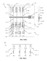
The programmable resistive devices can be used to construct a memory in accordance with one embodiment. FIG. 15 shows a portion of a programmable resistive memory 100 constructed by an array 101 of n-row by (m+1)-column single-diode-as-program-selector cells 110 and n wordline drivers 150-i, where i=0, 1, . . . , n−1, in accordance with one embodiment. The memory array 101 has m normal columns and one reference column for one shared sense amplifier 140 for differential sensing. Each of the memory cells 110 has a resistive element 111 coupled to the P terminal of a diode 112 as program selector and to a bitline BLj 170-j (j=0, 1, . . . m−1) or reference bitline BLR0 175-0 for those of the memory cells 110 in the same column. The N terminal of the diode 112 is coupled to a wordline WLBi 152-i through a local wordline LWLBi 154-i, where i=0, 1, . . . , n−1, for those of the memory cells 110 in the same row. Each wordline WLBi is coupled to at least one local wordline LWLBi, where i=0, 1, . . . , n−1. The LWLBi 154-i is generally constructed by a high resistivity material, such as N well, polysilicon, polymetal, active region, extended source/drain, local interconnect, or metal gate, to connect cells, and then coupled to the WLBi (e.g., a low-resistivity metal WLBi) through conductive contacts or vias, buffers, or post-decoders 172-i, where i=0, 1, . . . , n−1. Buffers or post-decoders 172-i may be needed when using diodes as program selectors because there are currents flowing through the WLBi, especially when one WLBi drives multiple cells for program or read simultaneously in other embodiments. The wordline WLBi is driven by the wordline driver 150-i (i=0, 1, 2, . . . , n−1) with a supply voltage vddi that can be switched between different voltages for program and read. Each BLj 170-j or BLR0 175-0 is coupled to a supply voltage VDDP through a Y-write pass gate 120-j or 125 for programming, where each BLj 170-j or BLR0 175-0 is selected by YSWBj (j=0, 1, . . . , m−1) or YSWRB0, respectively. The Y-write pass gate 120-j (j=0, 1, . . . , m−1) or 125 can be built by PMOS, though NMOS, diode, or bipolar devices can be employed in some embodiments. Each BLj or BLR0 is coupled to a dataline DLj or DLR0 through a Y-read pass gate 130-j or 135 selected by YSRj (j=0, 1, . . . , m−1) or YSRR0, respectively. In this portion of memory array 101, m normal datalines DLj (j=0, 1, . . . , m−1) are connected to an input 160 of a sense amplifier 140. The reference dataline DLR0 provides another input 161 for the sense amplifier 140 (no multiplex is generally needed in the reference branch). The output of the sense amplifiers 140 is Q0. FIG. 15 can be readily applied to the programmable resistive cells that use MOS as program selector. The MOS program selectors in the cells can have the drains coupled to BLj, the gates coupled to LWLi and sources coupled to a ground line (VSS). The WLBi and LWLBi can be replaced by WLi and LWLi with polarity reversed, respectively, where i=0, 1, 2, . . . , n−1. The wordline and post-wordline drivers have the polarity reversed accordingly. The same can be applied to the reference cells, wordlines, or bitline.
To program a cell, the specific WLBi and YSWBj are turned on and a high voltage is supplied to VDDP, where i=0, 1, . . . n−1 and j=0, 1, . . . , m−1. In some embodiments, the reference cells can be programmed to 0 or 1 by turning on WLRBi, and YSWRB0, where i=0, 1, . . . , n−1. To read a cell, a data column 160 can be selected by turning on the specific WLBi and YSRj, where i=0, 1, . . . , n−1, and j=0, 1, . . . , m−1, and a reference cell coupled to the reference dataline DLR0 161 can be selected for the sense amplifier 140 to sense and compare the resistance difference between normal/reference BLs and ground, while disabling all YSWBj and YSWRB0 where j=0, 1, . . . , m−1.
The programmable resistive devices can be used to construct a memory in accordance with one embodiment. FIG. 16(a) shows a portion of a programmable resistive memory 100 constructed by an array 101 of 3-terminal MRAM cells 110 in n rows and m+1 columns with n pairs of wordline drivers 150-i and 151-i, where i=0, 1, . . . , n−1, according to one embodiment. The memory array 101 has m normal columns and one reference column for one shared sense amplifier 140 for differential sensing. Each of the memory cells 110 has a resistive element 111 coupled to the P terminal of a program-0 diode 112 and N terminal of a program-1 diode 113. The program-0 diode 112 and the program-1 diode 113 serve as program selectors. Each resistive element 111 is also coupled to a bitline BLj 170-j (j=0, 1, . . . m−1) or reference bitline BLR0 175-0 for those of the memory cells 110 in the same column. The N terminal of the diode 112 is coupled to a wordline WLNi 152-i through a local wordline LWLNi 154-i, where i=0, 1, . . . , n−1, for those of the memory cells 110 in the same row. The P terminal of the diode 113 is coupled to a wordline WLPi 153-i through a local wordline LWLPi 155-i, where i=0, 1, . . . , n−1, for those cells in the same row. Each wordline WLNi or WLPi is coupled to at least one local wordline LWLNi or LWLPi, respectively, where i=0, 1, . . . , n−1. The LWLNi 154-i and LWLPi 155-i are generally constructed by a high resistivity material, such as N well, polysilicon, local interconnect, active region, extended source/drain, or metal gate to connect cells, and then coupled to the WLNi or WLPi (e.g., low-resistivity metal WLNi or WLPi) through conductive contacts or vias, buffers, or post-decoders 172-i or 173-i respectively, where i=0, 1, . . . , n−1. Buffers or post-decoders 172-i or 173-i may be needed when using diodes as program selectors because there are currents flowing through WLNi or WLPi, especially when one WLNi or WLPi drivers multiple cells for program or read simultaneously in some embodiments. The wordlines WLNi and WLPi are driven by wordline drivers 150-i and 151-i, respectively, with a supply voltage vddi that can be switched between different voltages for program and read. Each BLj 170-j or BLR0 175-0 is coupled to a supply voltage VDDP through a Y-write-0 pass gate 120-j or 125 to program 0, where each BLj 170-j or BLR0 175-0 is selected by YS0WBj (j=0, 1, . . . , m−1) or YSOWRB0, respectively. Y-write-0 pass gate 120-j or 125 can be built by PMOS, though NMOS, diode, or bipolar devices can be employed in other embodiments. Similarly, each BLj 170-j or BLR0 175-0 is coupled to a supply voltage 0V through a Y-write-1 pass gate 121-j or 126 to program 1, where each BLj 170-j or BLR0 175-0 is selected by YS1Wj (j=0, 1, . . . , m−1) or YS1WR0, respectively. Y-write-1 pass gate 121-j or 126 can be built by NMOS, though PMOS, diode, or bipolar devices can be employed in other embodiments. Each BLj or BLR0 is coupled to a dataline DLj or DLR0 through a Y-read pass gate 130-j or 135 selected by YSRj (j=0, 1, . . . , m−1) or YSRR0, respectively. In this portion of memory array 101, m normal datalines DLj (j=0, 1, . . . , m−1) are connected to an input 160 of a sense amplifier 140. Reference dataline DLR0 provides another input 161 for the sense amplifier 140, except that no multiplex is generally needed in a reference branch. The output of the sense amplifier 140 is Q0.
To program a 0 into a cell, the specific WLNi, WLPi, and BLj are selected by wordline drivers 150-i and 151-i, and Y-pass gate 120-j (by YS0WBj), respectively, where i=0, 1, . . . n−1 and j=0, 1, . . . , m−1, while the other wordlines and bitlines are properly set. A high voltage is applied to VDDP. In some embodiments, the reference cells can be programmed into 0 by setting proper voltages to WLRNi 158-i, WLRPi 159-i and YSOWRB0, where i=0, 1, . . . , n−1. To program a 1 to a cell, the specific WLNi, WLPi and BLj are selected by wordline drivers 150-i, 151-i, and Y-pass gate 121-j (by YS1Wj), respectively, where i=0, 1, . . . n−1 and j=0, 1, . . . , m−1, while the other wordlines and bitlines are also properly set. In some embodiments, the reference cells can be programmed to 1 by setting proper voltages to WLRNi 158-i, WLRPi 159-i and YS1WR0, where i=0, 1, . . . , n−1. To read a cell, a data column 160 can be selected by turning on the specific WLNi, WLPi and YSRj, where i=0, 1, . . . , n−1, and j=0, 1, . . . , m−1, and a reference cell coupled to the reference dataline DLR 161 for the sense amplifier 140 to sense and compare the resistance difference between normal/reference BLs and ground, while disabling all YS0WBj, YSOWRB0, YS1Wj and YS1WR0, where j=0, 1, . . . , m−1.
Another embodiment of constructing an MRAM memory with 2-terminal MRAM cells is shown in FIG. 16(b) , provided the voltage difference between high and low states VDDP, is no more than twice of the diode's threshold voltage Vd, i.e., VDDP<2*Vd. As shown in FIG. 16(b) , two wordlines per row WLNi 152-i and WLPi 153-i in FIG. 16(a) can be merged into one wordline driver WLNi 152-i, where i=0, 1, . . . , n−1. Also, the local wordlines LWLNi 154-i and LWLP 155-i per row in FIG. 16(a) can be merged into one local wordline LWLNi 154-i, where i=0, 1, . . . , n−1, as shown in FIG. 16(b) . Still further, two wordline drivers 150-i and 151-i in FIG. 16(a) can be merged into one, i.e., wordline driver 150-i. The BLs and WLNs of the unselected cells can be applied with suitable supply voltages. Since half of wordlines, local wordlines, and wordline drivers can be eliminated in this embodiment, cell and macro areas can be reduced substantially.
Differential sensing is a common for programmable resistive memory, though single-end sensing can be used in other embodiments. FIGS. 17(a), 17(b), and 17(c) show three other embodiments of constructing reference cells for differential sensing. In FIG. 17(a) , a portion of memory 400 has a normal array 180 of n×m cells, two reference columns 150-0 and 150-1 of n×1 cells each storing all data 0 and 1 respectively, m+1 Y-read pass gates 130, and a sense amplifier 140. As an example, n=8 and m=8 are used to illustrate the concept. There are n wordlines WLBi and n reference wordlines WLRBi for each column, where i=0, 1, . . . , n−1. When a wordline WLBi is turned on to access a row, a corresponding reference wordline WLRBi (i=0, 1, . . . , n−1) is also turned on to activate two reference cells 170-0 and 170-1 in the same row to provide mid-level resistance after proper scaling in the sense amplifier. The selected dataline 160 along with the reference dataline 161 are input to a sense amplifier 140 to generate an output Q0. In this embodiment, each WLRBi and WLBi (i=0, 1, . . . , n−1) are hardwired together and every cells in the reference columns need to be pre-programmed before read.
For those programmable resistive devices that have a very small resistance ratio between states 1 and 0, such as 2:1 ratio in MRAM, FIGS. 17(a) and 17(c) are desirable embodiments, depending on how many cells are suitable for one pair of reference cells. Otherwise, FIG. 17(b) is a desirable embodiment for electrical fuse or PCM that has resistance ratio of more than about 10.
The portions of programmable resistive memories shown in FIGS. 15, 16 (a), 16(b), 17(a), 17(b) and 17(c) can include different types of resistive elements. The resistive element can be an electrical fuse including a fuse fabricated from an interconnect, contact/via fuse, contact/via anti-fuse, or gate oxide breakdown anti-fuse. Particularly, anti-fuse based on dielectric, junction, source/drain breakdown, or source/drain punch-through can be embodied easily in FinFET technologies. The interconnect fuse can be formed from silicide, polysilicon, silicided polysilicon, metal, metal alloy, local interconnect, thermally isolated active region, or some combination thereof, or can be constructed from a CMOS gate. The resistive element can also be fabricated from the elements in PCRAM, RRAM, CBRAM, or MRAM cells, etc. For the electrical fuse fabricated from an interconnect, contact, or via fuse, programming requirement is to provide a sufficiently high current, about 4-20 mA range, for a few microseconds to blow the fuse by electro-migration, heat, ion diffusion, or some combination thereof. For anti-fuse, programming requirement is to provide a sufficiently high voltage to breakdown the dielectric, junction, gate oxide, or source/drain between two ends of a contact, via, diode, CMOS gate/body, or CMOS source/drain. The required voltage is about 6-7V for a few millisecond to consume about 100 uA of current in today's technologies. Another type of anti-fuse can be applying a few milliamps of high current to punch-through the source/drain of a MOS. Programming Phase-Change Memory (PCM) requires different voltages and durations for 0 and 1. Programming to a 1 (or to reset) requires a high and short voltage pulse applied to the phase-change film. Alternatively, programming to a 0 (or to set) requires a low and long voltage pulse applied to the phase change film. The reset needs about 3V for 50 ns and consumes about 300 uA, while set needs about 2V for 300 ns and consumes about 100 uA. For MRAM, the high and low program voltages are about 2-3V and 0V, respectively, and the current is about +/−100-200 uA.
Most programmable resistive devices have a higher voltage VDDP (−2-3V) for programming than the core logic supply voltage VDD (−1.0V) for reading. FIG. 18(a) shows a schematic of a wordline driver circuit 60 according to one embodiment. The wordline driver includes devices 62 and 61, as shown as the wordline driver 150 in FIGS. 15, 16 (a) and 16(b). The supply voltage vddi is further coupled to either VDDP or VDD through power selectors 63 and 64 (e.g., PMOS power selectors) respectively. The input of the wordline driver Vin is from an output of an X-decoder. In some embodiments, the power selectors 63 and 64 are implemented as thick oxide I/O devices to sustain high voltage. The bodies of power selector 63 and 64 can be tied to vddi to prevent latchup.
Similarly, bitlines tend to have a higher voltage VDDP (−2-3V) for programming than the core logic supply voltage VDD (−1.0V) for reading. FIG. 18(b) shows a schematic of a bitline circuit 70 according to one embodiment. The bitline circuit 70 includes a bitline (BL) coupled to VDDP and VDD through power selectors 73 and 74 (e.g., PMOS power selectors), respectively. If the bitline needs to sink a current such as in an MRAM, an NMOS pulldown device 71 can be provided. In some embodiments, the power selectors 73 and 74 as well as the pulldown device 71 can be implemented as thick-oxide I/O devices to sustain high voltage. The bodies of power selector 73 and 74 can be tied to vddi to prevent latchup.
Using junction diodes as program selectors may have high leakage current if a memory size is very large. Power selectors for a memory can help reducing leakage current by switching to a lower supply voltage or even turning off when a portion of memory is not in use. FIG. 18(c) shows a portion of memory 85 with an internal power supply VDDP coupled to an external supply VDDPP and a core logic supply VDD through power selectors 83 and 84. VDDP can even be coupled to ground by an NMOS pulldown device 81 to disable this portion of memory 85, if this portion of memory is temporarily not in use.
The drains of MOS 130 and 131 are coupled to sources of NMOS 132 and 134, respectively. The gates of 132 and 134 are biased at a fixed voltage Vbias. The channel width to length ratios of NMOS 132 and 134 can be relatively large to clamp the voltage swings of dataline DL and reference dataline DLR, respectively. The drains of NMOS 132 and 134 are coupled to drains of PMOS 170 and 171, respectively. The drain of PMOS 170 is coupled to the gate of PMOS 171 and the drain of PMOS 171 is coupled to the gate of PMOS 170. The outputs V+ and V− of the pre-amplifier 100 are the drains of PMOS 170 and PMOS 171, respectively. The sources of PMOS 170 and PMOS 171 are coupled to a read supply voltage VDDR. The outputs V+ and V− are pulled up by a pair of PMOS 175 to VDDR when the pre-amplifier 100 is disabled. VDDR is about 2-3V (which is higher than about 1.0V VDD of core logic devices) to turn on the diode selectors 112 and 117 in the programmable resistive cell 110 and the reference cell 115, respectively. The CMOS 130, 131, 132, 134, 170, 171, and 175 can be embodied as thick-oxide I/O devices to sustain high voltage VDDR. The NMOS 132 and 134 can be native NMOS (i.e. the threshold voltage is −0V) to allow operating at a lower VDDR. In another embodiment, the read selectors 130 and 131 can be PMOS devices. In another embodiment, the sources of PMOS 170 and 171 can be coupled to the drain of a PMOS pullup (an activation device not shown in FIG. 19(a) ), whose source is then coupled to VDDR. This sense amplifier can be activated by setting the gate of the PMOS pullup low after turning on the reference and Y-select pass gates.
The invention can be implemented in a part or all of an integrated circuit in a Printed Circuit Board (PCB), or in a system. The programmable resistive device can be fuse, anti-fuse, or emerging nonvolatile memory. The fuse can be silicided or non-silicided polysilicon fuse, thermally isolated active-region fuse, local interconnect fuse, metal fuse, contact fuse, or via fuse. The anti-fuse can be based on gate-oxide breakdown, contact or via breakdown with dielectrics in-between, junction or source/drain breakdown, or source/drain punch-through. The emerging nonvolatile memory can be Magnetic RAM (MRAM), Phase Change Memory (PCM), Conductive Bridge RAM (CBRAM), or Resistive RAM (RRAM). Though the program mechanisms are different, their logic states can be distinguished by different resistance values.
Additional information on programmable resistive memory structures and their formation and usage can be found in: (1) U.S. patent application Ser. No. 13/026,650, filed on Feb. 14, 2011 and entitled “CIRCUIT AND SYSTEM FOR USING A POLYSILICON DIODE AS PROGRAM SELECTOR FOR RESISTIVE DEVICES IN CMOS LOGIC PROCESSES,” which is hereby incorporated herein by reference; (2) U.S. patent application Ser. No. 13/026,725, filed on Feb. 14, 2011 and entitled “CIRCUIT AND SYSTEM FOR USING A JUNCTION DIODE AS PROGRAM SELECTOR FOR RESISTIVE DEVICES,” which is hereby incorporated herein by reference; (3) U.S. patent application Ser. No. 13/026,725, filed on Feb. 14, 2011 and entitled “CIRCUIT AND SYSTEM OF USING JUNCTION DIODE AS PROGRAM SELECTOR FOR RESISTIVE DEVICES IN CMOS LOGIC PROCESSES,” which is hereby incorporated herein by reference; (4) U.S. patent application Ser. No. 13/026,650, filed on Feb. 14, 2011 and entitled “CIRCUIT AND SYSTEM OF USING POLYSILICON DIODE AS PROGRAM SELECTOR FOR RESISTIVE DEVICES IN CMOS LOGIC PROCESSES,” which is hereby incorporated herein by reference; and (5) U.S. patent application Ser. No. 13/471,704, filed on May 15, 2012 and entitled “CIRCUIT AND SYSTEM FOR USING A JUNCTION DIODE AS PROGRAM SELECTOR FOR ONE-TIME PROGRAMMABLE DEVICES,” which is hereby incorporated herein by reference.
The above description and drawings are only to be considered illustrative of exemplary embodiments, which achieve the features and advantages of the present invention. Modifications and substitutions of specific process conditions and structures can be made without departing from the spirit and scope of the present invention.
The many features and advantages of the present invention are apparent from the written description and, thus, it is intended by the appended claims to cover all such features and advantages of the invention. Further, since numerous modifications and changes will readily occur to those skilled in the art, it is not desired to limit the invention to the exact construction and operation as illustrated and described. Hence, all suitable modifications and equivalents may be resorted to as falling within the scope of the invention.
Claims (41)
1. A programmable resistive memory, comprising:
a plurality of programmable resistive cells, at least one of the programmable resistive cells comprising:
a resistive element;
at least one fin structure coupled to the resistive element, the at least one fin structure being a semiconductor structure and including at least a first active region and a second active region, the first active region having a first type of dopant, and the second active region having the first type of dopant or the second type of dopant; and
a gate provided over at least a portion of the at least one fin structure, the gate being provided between the first and second active regions,
wherein at least a portion of the first and second active regions residing in a common well or on an isolated substrate.
2. A programmable resistive memory as recited in claim 1 , wherein an insulator material is provided between the gate and the at least a portion of the at least one fin structure.
3. A programmable resistive memory as recited in claim 1 , wherein the resistive element is coupled to a first supply voltage line, and wherein the first active region is coupled to the resistive element, the second active region is coupled to a second supply voltage line, and the gate is coupled to a third supply voltage line.
4. A programmable resistive memory as recited in claim 3 , wherein the resistive element is configured to be programmable by applying voltages to the first, second, and/or third supply voltage lines to thereby change the resistance of the resistive element into a different logic state.
5. A programmable resistive memory as recited in claim 1 , wherein the fin structure at least in part forms a MOS device or dummy-gate diode.
6. A programmable resistive memory as recited in claim 5 , wherein the first active region provides a first terminal of the MOS or the dummy-gate diode, and the second active region provides a second terminal of the MOS or the dummy-gate diode.
7. A programmable resistive memory as recited in claim 1 , wherein the gate or dummy gate is fabricated from a MOS gate.
8. A programmable resistive memory as recited in claim 1 , wherein the at least one of the first or the second active region is fabricated from sources or drains of CMOS devices, and wherein at least a portion of the first and second active regions reside in a CMOS well and/or in an isolated substrate.
9. A programmable resistive memory as recited in claim 1 , wherein the at least one of the first or the second active region has no more than two (2) contacts.
10. A programmable resistive memory as recited in claim 9 , wherein the at least one contact in the at least one active region is larger than the at least one contact outside of the programmable resistive memory cells.
11. A programmable resistive memory as recited in claim 9 , wherein the at least one contact in the at least one active region is substantially the same or wider than the active region or the resistive element.
12. A programmable resistive memory as recited in claim 1 , wherein the resistive element has a plurality of terminals, and wherein at least one of the terminals of the resistive element has no more than two (2) contacts.
13. A programmable resistive memory as recited in claim 12 , wherein the at least one contact in at least one of the terminals of the resistive element is larger than the at least one contact outside of the programmable resistive memory cells.
14. A programmable resistive memory as recited in claim 1 , wherein the resistive element has a plurality of terminals, and wherein at least one of the terminals of the resistive element has no more than one (1) contact.
15. A programmable resistive memory as recited in claim 1 , wherein the resistive element has a plurality of terminals, and wherein the resistive element has a length to width ratio of 0.5 to 8 between two closest contacts in the terminals of the resistive element.
16. A programmable resistive memory as recited in claim 1 , wherein the first and the second active regions are built on at least one extended source/drain region of the FinFETs.
17. A programmable resistive memory as recited in claim 16 , wherein the fin structure at least in part forms a diode, and wherein the diode as program selector is constructed from at least one extended source/drain region.
18. A programmable resistive memory as recited in claim 17 , wherein the resistive element has at least one extended source/drain region and built into the same structure of MOS or the diode as program selector.
19. A programmable resistive memory as recited in claim 1 , wherein the resistive element comprises at least one of polysilicon, silicided polysilicon, silicide, polymetal, metal, metal alloy, local interconnect, thermally isolated active region, extended source/drain region, CMOS gate, or combination thereof.
20. A programmable resistive memory as recited in claim 1 , wherein the resistive element is part of the fin and built into the same fin structure of MOS or dummy-gate diode as program selector.
21. A programmable resistive memory as recited in claim 1 , wherein the resistive element comprise a CMOS gate, and wherein at least a portion of the CMOS gate is a metal gate.
22. A programmable resistive memory as recited in claim 21 , wherein the CMOS gate has a portion of NMOS metal gate and a portion of PMOS metal gate.
23. A programmable resistive memory as recited in claim 1 , wherein the resistive element comprises at least one conductive contact or via.
24. A programmable resistive memory as recited in claim 1 , wherein the resistive element comprises an anti-fuse based on junction breakdown, source/drain breakdown, or source/drain punch-through of at least one FinFET or the extended source/drain region.
25. A programmable resistive memory as recited in claim 1 , wherein the programmable resistive memory is provided in an integrated circuit package having I/O voltages, and wherein the program voltage of the programmable resistive memory cell is substantially close to the I/O voltages.
26. An electronics system, comprising:
a processor; and
a programmable resistive memory operatively connected to the processor, the programmable resistive memory includes at least a plurality of programmable resistive cells for providing data storage, each of the programmable resistive cells comprising:
a resistive element coupled to a first supply voltage line;
at least one MOS device or diode built on at least one fin structure with at least one active region, the at least one active region including at least a first active region and a second active region, the first active region having a first type of dopant and the second region having the first type of dopant or a second type of dopant, the first active region providing a first terminal of the MOS device or a dummy-gate diode, the second active region providing a second terminal of the MOS device or the dummy-gate diode, at least one portion of the first or second active region residing in a common well or on an isolated substrate, the first active region being coupled to the resistive element and the second active region coupled to a second supply voltage line; and
a MOS gate or a dummy gate being coupled to a third supply voltage line;
wherein the at least one of the first or the second active region is fabricated from sources or drains of CMOS devices, and
wherein the programmable resistive element is configured to be programmable by applying voltages to the first, second, and/or third supply voltage lines to thereby change the resistance into a different logic state.
27. A programmable resistive memory, comprising:
a plurality of programmable resistive cells, at least one of the programmable resistive cells comprising:
a resistive element coupled to a first supply voltage line;
at least one fin structure of semiconductor material residing in a CMOS well or on a isolated substrate and being coupled to the resistive element, and including at least a first active region and a second active region, the first active region having a first type of dopant, and the second active region having the first type of dopant or the second type of dopant; and
a gate provided over at least a portion of the at least one fin structure, the gate dividing the fin structure into the first and second active regions.
28. A programmable resistive memory as recited in claim 27 , wherein an insulator material is provided between the gate and the at least a portion of the at least one fin structure.
29. A programmable resistive memory as recited in claim 27 , wherein the fin structure at least in part forms a MOS device or dummy-gate diode.
30. A programmable resistive memory as recited in claim 27 , wherein the at least one of the first or the second active region has no more than two (2) contacts.
31. A programmable resistive memory as recited in claim 30 , wherein the at least one contact in the at least one active region is larger than the at least one contact outside of the programmable resistive memory cells.
32. A programmable resistive memory as recited in claim 30 , wherein the at least one contact in the at least one active region is substantially the same or wider than the active region or the resistive element.
33. A programmable resistive memory as recited in claim 27 , wherein the resistive element has a plurality of terminals, and wherein at least one of the terminals of the resistive element has no more than two (2) contacts.
34. A programmable resistive memory as recited in claim 33 , wherein the at least one contact in at least one of the terminals of the resistive element is larger than the at least one contact outside of the programmable resistive memory cells.
35. A programmable resistive memory as recited in claim 27 , wherein the resistive element has a plurality of terminals, and wherein at least one of the terminals of the resistive element has no more than one (1) contact.
36. A programmable resistive memory as recited in claim 27 , wherein the resistive element has a plurality of terminals, and wherein the resistive element has a length to width ratio of 0.5 to 8 between two closest contacts in the terminals of the resistive element.
37. A programmable resistive memory as recited in claim 27 , wherein the first and the second active regions are built on at least one extended source/drain region of the FinFETs.
38. A programmable resistive memory as recited in claim 37 , wherein the fin structure at least in part forms a diode, and wherein the diode serves as a program selector and includes at least one extended source/drain region.
39. A programmable resistive memory as recited in claim 38 , wherein the resistive element has at least one extended source/drain region and built into the same structure of MOS or the diode as a program selector.
40. A programmable resistive memory as recited in claim 27 , wherein the resistive element is part of the fin and built into the same fin structure of MOS or dummy-gate diode as a program selector.
41. A programmable resistive memory as recited in claim 27 , wherein the resistive element comprises at least one conductive contact or via.
Priority Applications (5)
| Application Number | Priority Date | Filing Date | Title |
|---|---|---|---|
| US14/500,743 US9548109B2 (en) | 2011-02-14 | 2014-09-29 | Circuit and system of using FinFET for building programmable resistive devices |
| US15/365,584 US9881970B2 (en) | 2011-02-14 | 2016-11-30 | Programmable resistive devices using Finfet structures for selectors |
| US15/884,362 US10192615B2 (en) | 2011-02-14 | 2018-01-30 | One-time programmable devices having a semiconductor fin structure with a divided active region |
| US16/245,223 US10586832B2 (en) | 2011-02-14 | 2019-01-10 | One-time programmable devices using gate-all-around structures |
| US16/799,809 US11011577B2 (en) | 2011-02-14 | 2020-02-24 | One-time programmable memory using gate-all-around structures |
Applications Claiming Priority (4)
| Application Number | Priority Date | Filing Date | Title |
|---|---|---|---|
| US13/026,678 US8482972B2 (en) | 2010-08-20 | 2011-02-14 | Memory devices using a plurality of diodes as program selectors with at least one being a polysilicon diode |
| US201261595165P | 2012-02-06 | 2012-02-06 | |
| US13/761,097 US8848423B2 (en) | 2011-02-14 | 2013-02-06 | Circuit and system of using FinFET for building programmable resistive devices |
| US14/500,743 US9548109B2 (en) | 2011-02-14 | 2014-09-29 | Circuit and system of using FinFET for building programmable resistive devices |
Related Parent Applications (1)
| Application Number | Title | Priority Date | Filing Date |
|---|---|---|---|
| US13/761,097 Continuation US8848423B2 (en) | 2011-02-14 | 2013-02-06 | Circuit and system of using FinFET for building programmable resistive devices |
Related Child Applications (1)
| Application Number | Title | Priority Date | Filing Date |
|---|---|---|---|
| US15/365,584 Continuation US9881970B2 (en) | 2011-02-14 | 2016-11-30 | Programmable resistive devices using Finfet structures for selectors |
Publications (2)
| Publication Number | Publication Date |
|---|---|
| US20150014785A1 US20150014785A1 (en) | 2015-01-15 |
| US9548109B2 true US9548109B2 (en) | 2017-01-17 |
Family
ID=52276463
Family Applications (3)
| Application Number | Title | Priority Date | Filing Date |
|---|---|---|---|
| US13/761,097 Active US8848423B2 (en) | 2011-02-14 | 2013-02-06 | Circuit and system of using FinFET for building programmable resistive devices |
| US14/500,743 Active US9548109B2 (en) | 2011-02-14 | 2014-09-29 | Circuit and system of using FinFET for building programmable resistive devices |
| US15/365,584 Active US9881970B2 (en) | 2011-02-14 | 2016-11-30 | Programmable resistive devices using Finfet structures for selectors |
Family Applications Before (1)
| Application Number | Title | Priority Date | Filing Date |
|---|---|---|---|
| US13/761,097 Active US8848423B2 (en) | 2011-02-14 | 2013-02-06 | Circuit and system of using FinFET for building programmable resistive devices |
Family Applications After (1)
| Application Number | Title | Priority Date | Filing Date |
|---|---|---|---|
| US15/365,584 Active US9881970B2 (en) | 2011-02-14 | 2016-11-30 | Programmable resistive devices using Finfet structures for selectors |
Country Status (1)
| Country | Link |
|---|---|
| US (3) | US8848423B2 (en) |
Cited By (17)
| Publication number | Priority date | Publication date | Assignee | Title |
|---|---|---|---|---|
| US20170110512A1 (en) * | 2011-02-14 | 2017-04-20 | Attopsemi Technology Co., Ltd | Finfet Structures for Programmable Resistive Devices |
| US10192615B2 (en) * | 2011-02-14 | 2019-01-29 | Attopsemi Technology Co., Ltd | One-time programmable devices having a semiconductor fin structure with a divided active region |
| US10229746B2 (en) | 2010-08-20 | 2019-03-12 | Attopsemi Technology Co., Ltd | OTP memory with high data security |
| US10269945B2 (en) | 2017-06-08 | 2019-04-23 | Ubiq Semiconductor Corp. | Power transistor device |
| US10431673B2 (en) | 2017-06-09 | 2019-10-01 | Samsung Electronics Co., Ltd. | Semiconductor devices |
| US10535413B2 (en) | 2017-04-14 | 2020-01-14 | Attopsemi Technology Co., Ltd | Low power read operation for programmable resistive memories |
| US10586593B2 (en) | 2012-12-07 | 2020-03-10 | Attopsemi Technology Co., Ltd | Programmable resistive device and memory using diode as selector |
| US10586832B2 (en) | 2011-02-14 | 2020-03-10 | Attopsemi Technology Co., Ltd | One-time programmable devices using gate-all-around structures |
| US10726914B2 (en) | 2017-04-14 | 2020-07-28 | Attopsemi Technology Co. Ltd | Programmable resistive memories with low power read operation and novel sensing scheme |
| US10770160B2 (en) | 2017-11-30 | 2020-09-08 | Attopsemi Technology Co., Ltd | Programmable resistive memory formed by bit slices from a standard cell library |
| US10916317B2 (en) | 2010-08-20 | 2021-02-09 | Attopsemi Technology Co., Ltd | Programmable resistance memory on thin film transistor technology |
| US10923204B2 (en) | 2010-08-20 | 2021-02-16 | Attopsemi Technology Co., Ltd | Fully testible OTP memory |
| US10930509B2 (en) | 2017-06-20 | 2021-02-23 | Samsung Electronics Co., Ltd. | Semiconductor devices and methods of manufacturing the same |
| US11062786B2 (en) | 2017-04-14 | 2021-07-13 | Attopsemi Technology Co., Ltd | One-time programmable memories with low power read operation and novel sensing scheme |
| US11177436B2 (en) | 2019-04-25 | 2021-11-16 | International Business Machines Corporation | Resistive memory with embedded metal oxide fin for gradual switching |
| US11605673B2 (en) | 2020-12-09 | 2023-03-14 | International Business Machines Corporation | Dual resistive random-access memory with two transistors |
| US11615859B2 (en) | 2017-04-14 | 2023-03-28 | Attopsemi Technology Co., Ltd | One-time programmable memories with ultra-low power read operation and novel sensing scheme |
Families Citing this family (101)
| Publication number | Priority date | Publication date | Assignee | Title |
|---|---|---|---|---|
| US8665629B2 (en) * | 2007-09-28 | 2014-03-04 | Qimonda Ag | Condensed memory cell structure using a FinFET |
| US9224496B2 (en) | 2010-08-11 | 2015-12-29 | Shine C. Chung | Circuit and system of aggregated area anti-fuse in CMOS processes |
| US9070437B2 (en) | 2010-08-20 | 2015-06-30 | Shine C. Chung | Circuit and system of using junction diode as program selector for one-time programmable devices with heat sink |
| US9019742B2 (en) | 2010-08-20 | 2015-04-28 | Shine C. Chung | Multiple-state one-time programmable (OTP) memory to function as multi-time programmable (MTP) memory |
| US8488359B2 (en) | 2010-08-20 | 2013-07-16 | Shine C. Chung | Circuit and system of using junction diode as program selector for one-time programmable devices |
| US10249379B2 (en) | 2010-08-20 | 2019-04-02 | Attopsemi Technology Co., Ltd | One-time programmable devices having program selector for electrical fuses with extended area |
| US9236141B2 (en) | 2010-08-20 | 2016-01-12 | Shine C. Chung | Circuit and system of using junction diode of MOS as program selector for programmable resistive devices |
| US9042153B2 (en) | 2010-08-20 | 2015-05-26 | Shine C. Chung | Programmable resistive memory unit with multiple cells to improve yield and reliability |
| US9496033B2 (en) | 2010-08-20 | 2016-11-15 | Attopsemi Technology Co., Ltd | Method and system of programmable resistive devices with read capability using a low supply voltage |
| US9824768B2 (en) | 2015-03-22 | 2017-11-21 | Attopsemi Technology Co., Ltd | Integrated OTP memory for providing MTP memory |
| US9460807B2 (en) | 2010-08-20 | 2016-10-04 | Shine C. Chung | One-time programmable memory devices using FinFET technology |
| US9431127B2 (en) | 2010-08-20 | 2016-08-30 | Shine C. Chung | Circuit and system of using junction diode as program selector for metal fuses for one-time programmable devices |
| US9251893B2 (en) | 2010-08-20 | 2016-02-02 | Shine C. Chung | Multiple-bit programmable resistive memory using diode as program selector |
| US8804398B2 (en) | 2010-08-20 | 2014-08-12 | Shine C. Chung | Reversible resistive memory using diodes formed in CMOS processes as program selectors |
| US9711237B2 (en) | 2010-08-20 | 2017-07-18 | Attopsemi Technology Co., Ltd. | Method and structure for reliable electrical fuse programming |
| US8830720B2 (en) | 2010-08-20 | 2014-09-09 | Shine C. Chung | Circuit and system of using junction diode as program selector and MOS as read selector for one-time programmable devices |
| US8482972B2 (en) | 2010-08-20 | 2013-07-09 | Shine C. Chung | Memory devices using a plurality of diodes as program selectors with at least one being a polysilicon diode |
| US9025357B2 (en) | 2010-08-20 | 2015-05-05 | Shine C. Chung | Programmable resistive memory unit with data and reference cells |
| US8988965B2 (en) | 2010-11-03 | 2015-03-24 | Shine C. Chung | Low-pin-count non-volatile memory interface |
| US9019791B2 (en) | 2010-11-03 | 2015-04-28 | Shine C. Chung | Low-pin-count non-volatile memory interface for 3D IC |
| US9076513B2 (en) | 2010-11-03 | 2015-07-07 | Shine C. Chung | Low-pin-count non-volatile memory interface with soft programming capability |
| US8913449B2 (en) | 2012-03-11 | 2014-12-16 | Shine C. Chung | System and method of in-system repairs or configurations for memories |
| CN102544011A (en) | 2010-12-08 | 2012-07-04 | 庄建祥 | Anti-fuse memory and electronic system |
| US8912576B2 (en) | 2011-11-15 | 2014-12-16 | Shine C. Chung | Structures and techniques for using semiconductor body to construct bipolar junction transistors |
| US9136261B2 (en) | 2011-11-15 | 2015-09-15 | Shine C. Chung | Structures and techniques for using mesh-structure diodes for electro-static discharge (ESD) protection |
| US9324849B2 (en) | 2011-11-15 | 2016-04-26 | Shine C. Chung | Structures and techniques for using semiconductor body to construct SCR, DIAC, or TRIAC |
| US9007804B2 (en) | 2012-02-06 | 2015-04-14 | Shine C. Chung | Circuit and system of protective mechanisms for programmable resistive memories |
| US8917533B2 (en) | 2012-02-06 | 2014-12-23 | Shine C. Chung | Circuit and system for testing a one-time programmable (OTP) memory |
| US8861249B2 (en) | 2012-02-06 | 2014-10-14 | Shine C. Chung | Circuit and system of a low density one-time programmable memory |
| US8629420B1 (en) * | 2012-07-03 | 2014-01-14 | Intel Mobile Communications GmbH | Drain extended MOS device for bulk FinFET technology |
| US9257197B2 (en) * | 2012-07-06 | 2016-02-09 | Micron Technology, Inc. | Apparatuses and/or methods for operating a memory cell as an anti-fuse |
| US9076526B2 (en) | 2012-09-10 | 2015-07-07 | Shine C. Chung | OTP memories functioning as an MTP memory |
| US9183897B2 (en) | 2012-09-30 | 2015-11-10 | Shine C. Chung | Circuits and methods of a self-timed high speed SRAM |
| US9230685B2 (en) | 2012-10-23 | 2016-01-05 | Micron Technology, Inc. | Memory programming methods and memory systems |
| US9324447B2 (en) | 2012-11-20 | 2016-04-26 | Shine C. Chung | Circuit and system for concurrently programming multiple bits of OTP memory devices |
| US9006087B2 (en) * | 2013-02-07 | 2015-04-14 | International Business Machines Corporation | Diode structure and method for wire-last nanomesh technologies |
| WO2015025441A1 (en) | 2013-08-23 | 2015-02-26 | パナソニック株式会社 | Semiconductor integrated circuit device |
| CN108922887B (en) * | 2013-09-04 | 2022-12-09 | 株式会社索思未来 | Semiconductor device with a plurality of semiconductor chips |
| KR102127866B1 (en) | 2013-10-30 | 2020-06-30 | 삼성디스플레이 주식회사 | Voltage generation integrated circuit and display apparatus having them |
| US9123414B2 (en) | 2013-11-22 | 2015-09-01 | Micron Technology, Inc. | Memory systems and memory programming methods |
| US9336875B2 (en) | 2013-12-16 | 2016-05-10 | Micron Technology, Inc. | Memory systems and memory programming methods |
| US10176868B2 (en) | 2013-12-20 | 2019-01-08 | Micron Technology, Inc. | Memory systems and memory programming methods |
| US9269432B2 (en) | 2014-01-09 | 2016-02-23 | Micron Technology, Inc. | Memory systems and memory programming methods |
| KR20150104362A (en) | 2014-03-05 | 2015-09-15 | 에스케이하이닉스 주식회사 | Semiconductor device having buried gate and manufacturing method of the same |
| CN106030812B (en) * | 2014-03-27 | 2019-09-24 | 英特尔公司 | Germanium tin channel transistor |
| US9953989B2 (en) * | 2014-03-31 | 2018-04-24 | Taiwan Semiconductor Manufacturing Company Limited and National Taiwan University | Antifuse array and method of forming antifuse using anodic oxidation |
| US9528194B2 (en) | 2014-03-31 | 2016-12-27 | Taiwan Semiconductor Manufacturing Company Limited & National Taiwan University | Systems and methods for forming nanowires using anodic oxidation |
| CN104979362B (en) | 2014-04-10 | 2019-11-19 | 三星电子株式会社 | Semiconductor device with finned active patterns and gate node |
| US9412473B2 (en) | 2014-06-16 | 2016-08-09 | Shine C. Chung | System and method of a novel redundancy scheme for OTP |
| KR102179169B1 (en) | 2014-09-02 | 2020-11-18 | 삼성전자주식회사 | Semiconductor device and method for manufacturing semiconductor device |
| KR102358054B1 (en) | 2014-09-29 | 2022-02-04 | 삼성전자주식회사 | memory device including one-time programmable memory cells |
| US9293221B1 (en) | 2015-02-26 | 2016-03-22 | International Business Machines Corporation | Three terminal fuse with FinFET |
| US9768276B2 (en) | 2015-04-23 | 2017-09-19 | International Business Machines Corporation | Method and structure of forming FinFET electrical fuse structure |
| US9761584B2 (en) | 2015-06-05 | 2017-09-12 | Taiwan Semiconductor Manufacturing Co., Ltd. | Buried channel semiconductor device and method for manufacturing the same |
| US11063559B2 (en) | 2015-06-05 | 2021-07-13 | Taiwan Semiconductor Manufacturing Co., Ltd. | High-implant channel semiconductor device and method for manufacturing the same |
| TWI606448B (en) | 2015-07-29 | 2017-11-21 | 國立交通大學 | Dielectric fuse memory circuit and operation method thereof |
| US9825093B2 (en) | 2015-08-21 | 2017-11-21 | Globalfoundries Inc. | FinFET PCM access transistor having gate-wrapped source and drain regions |
| US9583624B1 (en) | 2015-09-25 | 2017-02-28 | International Business Machines Corporation | Asymmetric finFET memory access transistor |
| KR102323943B1 (en) | 2015-10-21 | 2021-11-08 | 삼성전자주식회사 | Method of manufacturing semiconductor device |
| US9613899B1 (en) | 2015-11-02 | 2017-04-04 | International Business Machines Corporation | Epitaxial semiconductor fuse for FinFET structure |
| US9666527B1 (en) | 2015-12-15 | 2017-05-30 | International Business Machines Corporation | Middle of the line integrated eFuse in trench EPI structure |
| US9536926B1 (en) | 2015-12-22 | 2017-01-03 | International Business Machines Corporation | Magnetic tunnel junction based anti-fuses with cascoded transistors |
| US9768231B2 (en) | 2016-02-12 | 2017-09-19 | Globalfoundries Singapore Pte. Ltd. | High density multi-time programmable resistive memory devices and method of forming thereof |
| US10008507B2 (en) | 2016-04-14 | 2018-06-26 | International Business Machines Corporation | Metal FinFET anti-fuse |
| KR102106664B1 (en) * | 2016-06-22 | 2020-05-06 | 매그나칩 반도체 유한회사 | OTP Cell and OTP Memory Array Using the Same |
| TWI594421B (en) * | 2016-06-28 | 2017-08-01 | 瑞昱半導體股份有限公司 | Finfet and manufacturing method of the same |
| US9735165B1 (en) | 2016-07-21 | 2017-08-15 | International Business Machines Corporation | Vertically stacked FinFET fuse |
| US10032784B2 (en) * | 2016-07-27 | 2018-07-24 | Synopsys, Inc. | One-time programmable bitcell with native anti-fuse |
| US9589970B1 (en) * | 2016-08-02 | 2017-03-07 | United Microelectronics Corp. | Antifuse one-time programmable memory |
| US10109791B2 (en) * | 2016-08-24 | 2018-10-23 | Euipil Kwon | Nonvolatile memory device and method of fabricating the same |
| CN107799421B (en) * | 2016-09-05 | 2021-04-02 | 中芯国际集成电路制造(上海)有限公司 | Method for forming semiconductor device |
| US9831254B1 (en) | 2016-09-22 | 2017-11-28 | International Business Machines Corporation | Multiple breakdown point low resistance anti-fuse structure |
| US10395745B2 (en) | 2016-10-21 | 2019-08-27 | Synposys, Inc. | One-time programmable bitcell with native anti-fuse |
| CN108074871B (en) * | 2016-11-11 | 2020-06-09 | 中芯国际集成电路制造(上海)有限公司 | Dynamic random access memory and forming method thereof |
| CN108133946B (en) * | 2016-12-01 | 2020-10-16 | 中芯国际集成电路制造(上海)有限公司 | Semiconductor device and method for manufacturing the same |
| US10446562B1 (en) | 2017-01-10 | 2019-10-15 | Synopsys, Inc. | One-time programmable bitcell with partially native select device |
| US10319662B2 (en) * | 2017-02-01 | 2019-06-11 | Indian Institute Of Science | Non-planar electrostatic discharge (ESD) protection devices with nano heat sinks |
| WO2018182636A1 (en) * | 2017-03-30 | 2018-10-04 | Intel Corporation | Integrated fuse in local interconnect and techniques for forming |
| US10756267B2 (en) * | 2017-04-11 | 2020-08-25 | National Chiao Tung University | Nonvolatile memory comprising variable resistance transistors and method for operating the same |
| US10354710B2 (en) * | 2017-07-24 | 2019-07-16 | Sandisk Technologies Llc | Magnetoelectric random access memory array and methods of operating the same |
| US10573596B2 (en) | 2017-12-08 | 2020-02-25 | International Business Machines Corporation | FinFET fuses formed at tight pitch dimensions |
| US10693056B2 (en) | 2017-12-28 | 2020-06-23 | Spin Memory, Inc. | Three-dimensional (3D) magnetic memory device comprising a magnetic tunnel junction (MTJ) having a metallic buffer layer |
| US10803916B2 (en) | 2017-12-29 | 2020-10-13 | Spin Memory, Inc. | Methods and systems for writing to magnetic memory devices utilizing alternating current |
| US10192789B1 (en) | 2018-01-08 | 2019-01-29 | Spin Transfer Technologies | Methods of fabricating dual threshold voltage devices |
| US10770510B2 (en) * | 2018-01-08 | 2020-09-08 | Spin Memory, Inc. | Dual threshold voltage devices having a first transistor and a second transistor |
| US10319424B1 (en) | 2018-01-08 | 2019-06-11 | Spin Memory, Inc. | Adjustable current selectors |
| US10797223B2 (en) | 2018-01-29 | 2020-10-06 | Globalfoundries Singapore Pte. Ltd. | Integrated circuits with magnetic random access memory (MRAM) devices and methods for fabricating such devices |
| US10855287B2 (en) * | 2018-02-20 | 2020-12-01 | United States Of America, As Represented By The Secretary Of The Navy | Non-volatile multiple time programmable integrated circuit system with selective conversion to one time programmable or permanent configuration bit programming capabilities and related methods |
| US10290340B1 (en) * | 2018-03-29 | 2019-05-14 | Qualcomm Technologies, Incorporated | Offset-canceling (OC) write operation sensing circuits for sensing switching in a magneto-resistive random access memory (MRAM) bit cell in an MRAM for a write operation |
| US10553646B2 (en) * | 2018-06-28 | 2020-02-04 | Microsemi Soc Corp. | Circuit and layout for resistive random-access memory arrays |
| US10553643B2 (en) | 2018-06-28 | 2020-02-04 | Microsemi Soc Corp. | Circuit and layout for resistive random-access memory arrays having two bit lines per column |
| DE102019114436A1 (en) * | 2018-08-20 | 2020-02-20 | Taiwan Semiconductor Manufacturing Company, Ltd. | EFUSE CIRCUIT, METHOD, STRUCTURE AND STRUCTURE |
| US10692556B2 (en) | 2018-09-28 | 2020-06-23 | Spin Memory, Inc. | Defect injection structure and mechanism for magnetic memory |
| US10878870B2 (en) | 2018-09-28 | 2020-12-29 | Spin Memory, Inc. | Defect propagation structure and mechanism for magnetic memory |
| US10991756B2 (en) * | 2018-10-23 | 2021-04-27 | Taiwan Semiconductor Manufacturing Co., Ltd. | Bipolar selector with independently tunable threshold voltages |
| CN111354849B (en) * | 2018-12-24 | 2023-06-30 | 联华电子股份有限公司 | Semiconductor element and manufacturing method thereof |
| CN112234077B (en) | 2019-07-15 | 2024-03-22 | 联华电子股份有限公司 | Magnetic memory cell and method of making the same |
| US10892222B1 (en) * | 2019-09-04 | 2021-01-12 | Globalfoundries Inc. | Anti-fuse for an integrated circuit (IC) product and method of making such an anti-fuse for an IC product |
| US11502089B2 (en) * | 2020-10-05 | 2022-11-15 | Micron Technology, Inc. | Three-dimensional fuse architectures and related systems, methods, and apparatuses |
| CN112397544B (en) * | 2020-11-12 | 2021-09-14 | 长江先进存储产业创新中心有限责任公司 | Three-dimensional phase change memory and control method thereof |
| US11854625B2 (en) * | 2021-03-04 | 2023-12-26 | Taiwan Semiconductor Manufacturing Company, Ltd. | Device and method for operating the same |
Citations (209)
| Publication number | Priority date | Publication date | Assignee | Title |
|---|---|---|---|---|
| US3198670A (en) | 1961-03-09 | 1965-08-03 | Bunker Ramo | Multi-tunnel diode |
| US3715242A (en) | 1969-12-17 | 1973-02-06 | Philips Corp | Methods of manufacturing semiconductor devices |
| US4148046A (en) | 1978-01-16 | 1979-04-03 | Honeywell Inc. | Semiconductor apparatus |
| US4192059A (en) | 1978-06-06 | 1980-03-11 | Rockwell International Corporation | Process for and structure of high density VLSI circuits, having inherently self-aligned gates and contacts for FET devices and conducting lines |
| US4642674A (en) | 1983-06-13 | 1987-02-10 | U.S. Philips Corporation | Field effect semiconductor device having improved voltage breakdown characteristics |
| JPH03264814A (en) | 1990-03-15 | 1991-11-26 | Pioneer Electron Corp | Nagivation apparatus for vehicle |
| US5192989A (en) | 1989-11-28 | 1993-03-09 | Nissan Motor Co., Ltd. | Lateral dmos fet device with reduced on resistance |
| US5389552A (en) | 1993-01-29 | 1995-02-14 | National Semiconductor Corporation | Transistors having bases with different shape top surfaces |
| US5447876A (en) | 1993-11-19 | 1995-09-05 | Micrel, Inc. | Method of making a diamond shaped gate mesh for cellular MOS transistor array |
| US5635742A (en) | 1994-02-02 | 1997-06-03 | Nissan Motor Co., Ltd. | Lateral double-diffused mosfet |
| US5637901A (en) | 1993-12-14 | 1997-06-10 | Analog Devices, Inc. | Integrated circuit with diode-connected transistor for reducing ESD damage |
| US5723890A (en) | 1994-01-07 | 1998-03-03 | Fuji Electric Co., Ltd. | MOS type semiconductor device |
| US5757046A (en) | 1994-01-07 | 1998-05-26 | Fuji Electric Company Ltd. | MOS type semiconductor device |
| US5761148A (en) | 1996-12-16 | 1998-06-02 | Cypress Semiconductor Corp. | Sub-word line driver circuit for memory blocks of a semiconductor memory device |
| US5962903A (en) | 1995-06-08 | 1999-10-05 | Taiwan Semiconductor Manufacturing Company, Ltd. | Planarized plug-diode mask ROM structure |
| US6002156A (en) | 1997-09-16 | 1999-12-14 | Winbond Electronics Corp. | Distributed MOSFET structure with enclosed gate for improved transistor size/layout area ratio and uniform ESD triggering |
| US6008092A (en) | 1996-02-12 | 1999-12-28 | International Rectifier Corporation | Short channel IGBT with improved forward voltage drop and improved switching power loss |
| US6034882A (en) | 1998-11-16 | 2000-03-07 | Matrix Semiconductor, Inc. | Vertically stacked field programmable nonvolatile memory and method of fabrication |
| US6054344A (en) | 1998-10-30 | 2000-04-25 | Taiwan Semiconductor Manufacturing Company | OTP (open trigger path) latchup scheme using buried-diode for sub-quarter micron transistors |
| US6140687A (en) | 1996-11-28 | 2000-10-31 | Matsushita Electric Industrial Co., Ltd. | High frequency ring gate MOSFET |
| US6243864B1 (en) | 1997-07-17 | 2001-06-05 | Matsushita Electric Industrial Co., Ltd. | Compiler for optimizing memory instruction sequences by marking instructions not having multiple memory address paths |
| US6249472B1 (en) | 1997-12-25 | 2001-06-19 | Texas Instruments Incorporated | Semiconductor memory device with antifuse |
| US6346727B1 (en) | 1998-01-07 | 2002-02-12 | Nec Corporation | Semiconductor device having optimized two-dimensional array of double diffused MOS field effect transistors |
| US20020018355A1 (en) | 1998-11-16 | 2002-02-14 | Johnson Mark G. | Vertically stacked field programmable nonvolatile memory and method of fabrication |
| US6400540B1 (en) | 1999-03-12 | 2002-06-04 | Sil.Able Inc. | Clamp circuit to prevent ESD damage to an integrated circuit |
| US6405160B1 (en) | 1998-08-03 | 2002-06-11 | Motorola, Inc. | Memory compiler interface and methodology |
| US20020075744A1 (en) | 2000-12-20 | 2002-06-20 | Mccollum John | Antifuse memory cell and antifuse memory cell array |
| US6461934B2 (en) | 1998-11-13 | 2002-10-08 | Mitsubishi Denki Kabushiki Kaisha | Method of manufacturing semiconductor device having trench type element isolation regions |
| US20020168821A1 (en) | 1999-04-22 | 2002-11-14 | Advanced Analogic Technologies, Inc. | Fabrication process for a super-self-aligned trench-gated DMOS with reduced on-resistance |
| US6483734B1 (en) | 2001-11-26 | 2002-11-19 | Hewlett Packard Company | Memory device having memory cells capable of four states |
| US20020196659A1 (en) | 2001-06-05 | 2002-12-26 | Hurst Terril N. | Non-Volatile memory |
| US20030104860A1 (en) | 2001-11-30 | 2003-06-05 | Anchor Gaming | Method, apparatus and system for perpetual bonus game |
| US20030135709A1 (en) | 2001-02-23 | 2003-07-17 | Niles Ronald Steven | Dynamic allocation of computer memory |
| US6597629B1 (en) | 2001-11-30 | 2003-07-22 | Virage Locic Corp. | Built-in precision shutdown apparatus for effectuating self-referenced access timing scheme |
| US6611043B2 (en) | 2000-03-15 | 2003-08-26 | Nec Corporation | Bipolar transistor and semiconductor device having the same |
| US20030169625A1 (en) | 2002-03-05 | 2003-09-11 | Glen Hush | Programmable conductor random access memory and method for sensing same |
| EP1367596A1 (en) | 2002-05-31 | 2003-12-03 | Hewlett-Packard Company | Cross-point diode ROM |
| CN1469473A (en) | 2002-07-15 | 2004-01-21 | �����ɷ� | IC device and its manufacture |
| US20040057271A1 (en) | 2002-09-25 | 2004-03-25 | Ward Parkinson | Method of operating programmable resistant element |
| US6731535B1 (en) | 2002-12-10 | 2004-05-04 | Renesas Technology Corp. | Nonvolatile semiconductor memory device |
| US20040113183A1 (en) | 2002-12-13 | 2004-06-17 | Ilya Karpov | Isolating phase change memory devices |
| US20040130924A1 (en) | 2000-05-31 | 2004-07-08 | Ma Stanley Jeh-Chun | Multiple match detection circuit and method |
| US6770953B2 (en) | 2000-01-31 | 2004-08-03 | Infineon Technologies Ag | Bipolar transistor |
| US6798684B2 (en) | 2002-04-04 | 2004-09-28 | Broadcom Corporation | Methods and systems for programmable memory using silicided poly-silicon fuses |
| US6803804B2 (en) | 2002-05-24 | 2004-10-12 | Raminda U. Madurawe | Programmable latch array using antifuses |
| US6813705B2 (en) | 2000-02-09 | 2004-11-02 | Hewlett-Packard Development Company, L.P. | Memory disambiguation scheme for partially redundant load removal |
| US20050060500A1 (en) | 2003-09-11 | 2005-03-17 | Taiwan Semiconductor Manufacturing Company, Ltd. | General purpose memory compiler system and associated methods |
| US20050062110A1 (en) | 2003-09-18 | 2005-03-24 | Franz Dietz | Semiconductor over-voltage protection structure for integrated circuit and for diode |
| US6897543B1 (en) | 2003-08-22 | 2005-05-24 | Altera Corporation | Electrically-programmable integrated circuit antifuses |
| US20050110081A1 (en) | 2003-11-25 | 2005-05-26 | Texas Instruments Incorporated | Drain extended MOS transistor with improved breakdown robustness |
| US20050124116A1 (en) | 2003-12-08 | 2005-06-09 | Tzu-Hsuan Hsu | 3D polysilicon ROM and method of fabrication thereof |
| US20050146962A1 (en) | 2002-02-15 | 2005-07-07 | John Schreck | Physically alternating sense amplifier activation |
| US6944083B2 (en) | 2003-11-17 | 2005-09-13 | Sony Corporation | Method for detecting and preventing tampering with one-time programmable digital devices |
| CN1691204A (en) | 2004-01-05 | 2005-11-02 | 国际商业机器公司 | Memory cells using gated diodes and methods of use thereof |
| US20050242386A1 (en) | 2004-04-29 | 2005-11-03 | Kern-Huat Ang | Memory cell and method of fabricating the same |
| US6967879B2 (en) | 2002-11-20 | 2005-11-22 | Matsushita Electric Industrial Co., Ltd. | Memory trouble relief circuit |
| US7009182B2 (en) | 2001-05-14 | 2006-03-07 | Department Of Atomic Energy, Government Of India | Low cost digital pocket dosemeter |
| US20060072357A1 (en) | 2004-10-01 | 2006-04-06 | Wicker Guy C | Method of operating a programmable resistance memory array |
| US20060092689A1 (en) | 2004-11-04 | 2006-05-04 | Daniel Braun | Reference current source for current sense amplifier and programmable resistor configured with magnetic tunnel junction cells |
| US20060104111A1 (en) | 2004-11-17 | 2006-05-18 | Spansion Llc | Diode array architecture for addressing nanoscale resistive memory arrays |
| US20060120148A1 (en) | 2004-10-26 | 2006-06-08 | Samsung Electronics Co., Ltd. | Semiconductor memory device with stacked memory cell and method of manufacturing the stacked memory cell |
| US20060129782A1 (en) | 2004-12-15 | 2006-06-15 | Sorav Bansal | Apparatus, system, and method for dynamically allocating main memory among a plurality of applications |
| US7102951B2 (en) | 2004-11-01 | 2006-09-05 | Intel Corporation | OTP antifuse cell and cell array |
| US20060215440A1 (en) | 2005-03-24 | 2006-09-28 | Beak-Hyung Cho | Nonvolatile memory devices having enhanced bit line and/or word line driving capability |
| US20060244099A1 (en) | 2004-05-06 | 2006-11-02 | Wlodek Kurjanowicz | Split-channel antifuse array architecture |
| US20070004160A1 (en) | 2004-01-07 | 2007-01-04 | Voldman Steven H | Tunable semiconductor diodes |
| US7167397B2 (en) | 2005-06-21 | 2007-01-23 | Intel Corporation | Apparatus and method for programming a memory array |
| US20070057323A1 (en) | 2005-09-12 | 2007-03-15 | International Business Machines Corporation | Silicon-on-insulator (soi) read only memory (rom) array and method of making a soi rom |
| US20070081377A1 (en) | 2005-09-26 | 2007-04-12 | Macronix International Co., Ltd. | Method and circuit for reading fuse cells in a nonvolatile memory during power-up |
| US7212432B2 (en) | 2004-09-30 | 2007-05-01 | Infineon Technologies Ag | Resistive memory cell random access memory device and method of fabrication |
| US7211843B2 (en) | 2002-04-04 | 2007-05-01 | Broadcom Corporation | System and method for programming a memory cell |
| US7224598B2 (en) | 2004-09-02 | 2007-05-29 | Hewlett-Packard Development Company, L.P. | Programming of programmable resistive memory devices |
| US20070133341A1 (en) | 2002-07-05 | 2007-06-14 | Aplus Flash Technology, Inc. | Combination nonvolatile memory using unified technology with byte, page and block write and simultaneous read and write operations |
| US20070138549A1 (en) | 2005-12-19 | 2007-06-21 | Schyi-Yi Wu | Gate layouts for transistors |
| US7263027B2 (en) | 2004-10-14 | 2007-08-28 | Broadcom Corporation | Integrated circuit chip having non-volatile on-chip memories for providing programmable functions and features |
| US20070223266A1 (en) | 2006-03-24 | 2007-09-27 | Macronix International Co., Ltd. | One-time-programmable (OTP) memory device and method for testing the same |
| US7294542B2 (en) | 2000-05-15 | 2007-11-13 | Nec Electronics Corporation | Method of fabricating a semiconductor device having CMOS transistors and a bipolar transistor |
| CN101083227A (en) | 2006-05-30 | 2007-12-05 | 旺宏电子股份有限公司 | Magnetic random access memory using single crystal self-aligned diode |
| US20080025068A1 (en) | 2006-07-31 | 2008-01-31 | Scheuerlein Roy E | Reverse bias trim operations in non-volatile memory |
| US20080028134A1 (en) | 1992-03-17 | 2008-01-31 | Kiyoshi Matsubara | Data line disturbance free memory block divided flash memory and microcomputer having flash memory therein |
| US20080044959A1 (en) | 2005-08-31 | 2008-02-21 | International Business Machines Corporation | Body-contacted semiconductor structures and methods of fabricating such body-contacted semiconductor structures |
| US20080067601A1 (en) | 2006-09-20 | 2008-03-20 | Himax Technologies Limited | Esd protection apparatus and circuit thereof |
| US7369452B2 (en) | 2006-04-07 | 2008-05-06 | Freescale Semiconductor, Inc. | Programmable cell |
| US20080105878A1 (en) | 2006-11-07 | 2008-05-08 | Elpida Memory, Inc. | Semiconductor storage device and method of manufacturing the same |
| CN101188140A (en) | 2006-11-21 | 2008-05-28 | 奇梦达北美公司 | Resistive memory including bipolar transistor access devices |
| US7391064B1 (en) | 2004-12-01 | 2008-06-24 | Spansion Llc | Memory device with a selection element and a control line in a substantially similar layer |
| US20080151612A1 (en) | 2005-06-03 | 2008-06-26 | Stmicroelectronics S.R.L. | Method for multilevel programming of phase change memory cells using a percolation algorithm |
| US20080170429A1 (en) | 2005-05-09 | 2008-07-17 | Nantero, Inc. | Nonvolatile nanotube diodes and nonvolatile nanotube blocks and systems using same and methods of making same |
| US20080175060A1 (en) | 2007-01-24 | 2008-07-24 | Kilopass Technology, Inc. | Non-volatile semiconductor memory based on enhanced gate oxide breakdown |
| US7411844B2 (en) | 2005-11-30 | 2008-08-12 | Infineon Technologies Flash Gmbh & Co. Kg | Semiconductor memory device having a redundancy information memory directly connected to a redundancy control circuit |
| US20080220560A1 (en) | 1997-10-01 | 2008-09-11 | Patrick Klersy | Programmable resistance memory element and method for making same |
| US20080225567A1 (en) | 2007-03-15 | 2008-09-18 | International Business Machines Corporation | Method and structure for increasing effective transistor width in memory arrays with dual bitlines |
| CN101271881A (en) | 2007-03-20 | 2008-09-24 | 联华电子股份有限公司 | Inverse fuse wire and memory cell without ability to cause non-linear current after fusing |
| US7439608B2 (en) | 2006-09-22 | 2008-10-21 | Intel Corporation | Symmetric bipolar junction transistor design for deep sub-micron fabrication processes |
| US20080316852A1 (en) | 2007-06-21 | 2008-12-25 | Kabushiki Kaisha Toshiba | Nonvolatile semiconductor memory device |
| TWI309081B (en) | 2005-09-28 | 2009-04-21 | Sandisk 3D Llc | Method for using a memory cell comprising switchable semiconductor memory element with trimmable resistance |
| US20090115021A1 (en) | 2007-11-02 | 2009-05-07 | Elpida Memory, Inc. | Antifuse element in which more than two values of information can be written |
| US20090172315A1 (en) | 2007-12-27 | 2009-07-02 | Ravishankar Iyer | Priority aware selective cache allocation |
| US20090168493A1 (en) | 2004-10-26 | 2009-07-02 | Samsung Electronics Co., Ltd | Semiconductor memory device with stacked memory cell and method of manufacturing the stacked memory cell |
| CN101483062A (en) | 2008-01-11 | 2009-07-15 | 株式会社东芝 | Resistance change type memory |
| US20090194839A1 (en) | 2005-11-15 | 2009-08-06 | Bertin Claude L | Nonvolatile nanotube diodes and nonvolatile nanotube blocks and systems using same and methods of making same |
| US7573762B2 (en) | 2007-06-06 | 2009-08-11 | Freescale Semiconductor, Inc. | One time programmable element system in an integrated circuit |
| US7579232B1 (en) | 2008-07-11 | 2009-08-25 | Sandisk 3D Llc | Method of making a nonvolatile memory device including forming a pillar shaped semiconductor device and a shadow mask |
| US20090213660A1 (en) | 2008-02-25 | 2009-08-27 | Tower Semiconductor Ltd. | Three-Terminal Single Poly NMOS Non-Volatile Memory Cell |
| US20090219756A1 (en) | 2008-02-28 | 2009-09-03 | Peter Schroegmeier | Apparatus and Method for Determining a Memory State of a Resistive N-Level Memory Cell and Memory Device |
| US7589367B2 (en) | 2005-04-08 | 2009-09-15 | Samsung Electronics Co., Ltd. | Layout structure in semiconductor memory device comprising global work lines, local work lines, global bit lines and local bit lines |
| US7609578B2 (en) | 2007-10-31 | 2009-10-27 | Broadcom Corporation | Quad SRAM based one time programmable memory |
| US20090309089A1 (en) | 2008-06-13 | 2009-12-17 | Kang-Jay Hsia | Non-Volatile Memory Arrays Comprising Rail Stacks with a Shared Diode Component Portion for Diodes of Electrically Isolated Pillars |
| US20100027326A1 (en) | 2008-07-30 | 2010-02-04 | Ho Jung Kim | Memory device, memory system having the same, and programming method of a memory cell |
| US7660181B2 (en) | 2002-12-19 | 2010-02-09 | Sandisk 3D Llc | Method of making non-volatile memory cell with embedded antifuse |
| US20100061136A1 (en) | 2008-09-05 | 2010-03-11 | Semiconductor Energy Laboratory Co., Ltd. | Semiconductor Memory Device and Semiconductor Device |
| US20100085798A1 (en) | 2008-10-08 | 2010-04-08 | The Regents Of The University Of Michigan | Silicon-based nanoscale resistive device with adjustable resistance |
| US20100091546A1 (en) | 2008-10-15 | 2010-04-15 | Seagate Technology Llc | High density reconfigurable spin torque non-volatile memory |
| US7701038B2 (en) | 2005-10-31 | 2010-04-20 | Taiwan Semiconductor Manufacturing Company, Ltd. | High-gain vertex lateral bipolar junction transistor |
| CN101728412A (en) | 2008-11-03 | 2010-06-09 | 财团法人工业技术研究院 | Resistive memory array and cell |
| US20100142254A1 (en) | 2008-12-05 | 2010-06-10 | Byung-Gil Choi | Nonvolatile Memory Device Using Variable Resistive Element |
| US20100157651A1 (en) | 2008-12-18 | 2010-06-24 | Sandisk 3D Llc | Method of programming a nonvolatile memory device containing a carbon storage material |
| US20100171086A1 (en) | 2009-01-07 | 2010-07-08 | Macronix International Co., Ltd. | Integrated circuit memory with single crystal silicon on silicide driver and manufacturing method |
| US7764532B2 (en) | 2004-05-06 | 2010-07-27 | Sidense Corp. | High speed OTP sensing scheme |
| US7772591B1 (en) | 2004-02-17 | 2010-08-10 | Altera Corporation | Electrically-programmable transistor antifuses |
| US20100201410A1 (en) | 2009-02-06 | 2010-08-12 | Illegems Paul F | Power-up Control for Very Low-Power Systems |
| US20100232203A1 (en) | 2009-03-16 | 2010-09-16 | Taiwan Semiconductor Manufacturing Company, Ltd. | Electrical anti-fuse and related applications |
| US20100238701A1 (en) | 2009-03-23 | 2010-09-23 | Kabushiki Kaisha Toshiba | Semiconductor memory device |
| US20100246237A1 (en) | 2007-10-03 | 2010-09-30 | Bertrand Borot | Anti-fuse element |
| US7808815B2 (en) | 2006-10-02 | 2010-10-05 | Samsung Electronics Co., Ltd. | Variable resistance memory device and method of manufacturing the same |
| US20100277967A1 (en) | 2009-04-29 | 2010-11-04 | Macronix International Co., Ltd. | Graded metal oxide resistance based semiconductor memory device |
| US7830697B2 (en) | 2007-06-25 | 2010-11-09 | Sandisk 3D Llc | High forward current diodes for reverse write 3D cell |
| US20100301304A1 (en) | 2009-05-26 | 2010-12-02 | Macronix International Co., Ltd. | Buried silicide structure and method for making |
| US7852656B2 (en) | 2007-02-16 | 2010-12-14 | Magnachip Semiconductor Ltd. | One-time programmable cell and memory device having the same |
| US7859920B2 (en) | 2008-03-14 | 2010-12-28 | Qualcomm Incorporated | Advanced bit line tracking in high performance memory compilers |
| US20110022648A1 (en) | 2008-05-23 | 2011-01-27 | Harris Edward B | Secure Random Number Generator |
| US7889204B2 (en) | 1998-08-24 | 2011-02-15 | Microunity Systems Engineering, Inc. | Processor architecture for executing wide transform slice instructions |
| US20110062557A1 (en) | 2009-09-17 | 2011-03-17 | Abhijit Bandyopadhyay | 3d polysilicon diode with low contact resistance and method for forming same |
| US7910999B2 (en) | 2002-07-29 | 2011-03-22 | Taiwan Semiconductor Manufacturing Company | Method for four direction low capacitance ESD protection |
| US20110128772A1 (en) | 2009-12-02 | 2011-06-02 | Samsung Electronics Co., Ltd. | Nonvolatile memory cells and nonvolatile memory devices including the same |
| US20110145777A1 (en) | 2009-12-15 | 2011-06-16 | Sundar Iyer | Intelligent memory system compiler |
| US20110175199A1 (en) | 2010-01-18 | 2011-07-21 | Freescale Semiconductor, Inc. | Zener diode with reduced substrate current |
| US8008723B2 (en) | 2008-03-27 | 2011-08-30 | Renesas Electronics Corporation | Semiconductor device including a plurality of diffusion layers and diffusion resistance layer |
| US20110222330A1 (en) | 2010-03-11 | 2011-09-15 | Samsung Electronics Co., Ltd. | Nonvolatile memory device comprising one-time-programmable lock bit register |
| US20110260289A1 (en) | 2008-03-17 | 2011-10-27 | Seisei Oyamada | Semiconductor device and bypass capacitor module |
| US8050129B2 (en) | 2009-06-25 | 2011-11-01 | Mediatek Inc. | E-fuse apparatus for controlling reference voltage required for programming/reading e-fuse macro in an integrated circuit via switch device in the same integrated circuit |
| US20110267869A1 (en) | 2010-04-30 | 2011-11-03 | Hoefler Alexander B | Circuit for verifying the write enable of a one time programmable memory |
| US20110297912A1 (en) | 2010-06-08 | 2011-12-08 | George Samachisa | Non-Volatile Memory Having 3d Array of Read/Write Elements with Vertical Bit Lines and Laterally Aligned Active Elements and Methods Thereof |
| US20110310655A1 (en) | 2010-06-18 | 2011-12-22 | Franz Kreupl | Composition Of Memory Cell With Resistance-Switching Layers |
| US20110312166A1 (en) | 2003-05-20 | 2011-12-22 | Yedinak Joseph A | Methods of Manufacturing Power Semiconductor Devices with Shield and Gate Contacts |
| US20120032303A1 (en) | 2010-08-05 | 2012-02-09 | Elkareh Badih | Bipolar Junction Transistor Based on CMOS Technology |
| US8115280B2 (en) | 2005-10-31 | 2012-02-14 | Taiwan Semiconductor Manufacturing Company, Ltd. | Four-terminal gate-controlled LVBJTs |
| US20120039107A1 (en) | 2010-08-11 | 2012-02-16 | Chung Shine C | Circuit and System of Aggregated Area Anti-Fuse in CMOS Processes |
| US8119048B2 (en) | 2006-09-22 | 2012-02-21 | Nissha Printing Co., Ltd. | Housing case, method for manufacturing housing case, and glass insert molding die used in same |
| US20120044745A1 (en) | 2010-08-20 | 2012-02-23 | Chung Shine C | Reversible resistive memory using polysilicon diodes as program selectors |
| US20120047322A1 (en) | 2010-08-20 | 2012-02-23 | Chung Shine C | Method and System of Using One-Time Programmable Memory as Multi-Time Programmable in Code Memory of Processors |
| US20120044747A1 (en) | 2010-08-20 | 2012-02-23 | Chung Shine C | Reversible resistive memory using diodes formed in cmos processes as program selectors |
| US20120074460A1 (en) | 2010-09-21 | 2012-03-29 | Kabushiki Kaisha Toshiba | Semiconductor device and method for manufacturing the same |
| US20120106231A1 (en) | 2010-11-03 | 2012-05-03 | Chung Shine C | Low-pin-count non-volatile memory interface |
| US8174922B2 (en) | 2009-04-28 | 2012-05-08 | Renesas Electronics Corporation | Anti-fuse memory cell and semiconductor memory device |
| US8174063B2 (en) | 2009-07-30 | 2012-05-08 | Ememory Technology Inc. | Non-volatile semiconductor memory device with intrinsic charge trapping layer |
| US20120147657A1 (en) | 2009-06-19 | 2012-06-14 | Sekar Deepak C | Programming reversible resistance switching elements |
| US20120147653A1 (en) | 2010-12-08 | 2012-06-14 | Chung Shine C | Circuit and system of a high density anti-fuse |
| US8233316B2 (en) | 2006-05-18 | 2012-07-31 | Micron Technology, Inc. | Memory architecture and cell design employing two access transistors |
| US20120209888A1 (en) | 2011-02-15 | 2012-08-16 | Chung Shine C | Circuit and Method of a Memory Compiler Based on Subtraction Approach |
| US20120224406A1 (en) | 2010-08-20 | 2012-09-06 | Chung Shine C | Circuit and System of Using Junction Diode as Program Selector for One-Time Programmable Devices |
| US20120256292A1 (en) | 2011-04-08 | 2012-10-11 | Taiwan Semiconductor Manufacturing Company, Ltd. | Diodes with Embedded Dummy Gate Electrodes |
| US20120287730A1 (en) | 2011-05-11 | 2012-11-15 | Hynix Semiconductor Inc. | Non-volatile memory device and sensing method thereof |
| US20120314472A1 (en) | 2010-08-20 | 2012-12-13 | Chung Shine C | Multiple-Bit Programmable Resistive Memory Using Diode as Program Selector |
| US20120314473A1 (en) | 2010-08-20 | 2012-12-13 | Chung Shine C | Multiple-State One-Time Programmable (OTP) Memory to Function as Multi-Time Programmable (MTP) Memory |
| US20120320657A1 (en) | 2010-08-20 | 2012-12-20 | Chung Shine C | Programmable Resistive Memory Unit with Multiple Cells to Improve Yield and Reliability |
| US20120320656A1 (en) | 2010-08-20 | 2012-12-20 | Chung Shine C | Programmable Resistive Memory Unit with Data and Reference Cells |
| US8339079B2 (en) | 2007-09-12 | 2012-12-25 | Aisin Seiki Kabushiki Kaisha | Power semiconductor chip, power semiconductor module, inverter apparatus, and inverter-integrated motor |
| US8369166B2 (en) | 2009-07-27 | 2013-02-05 | Sidense Corp. | Redundancy system for non-volatile memory |
| US8373254B2 (en) | 2008-07-29 | 2013-02-12 | Taiwan Semiconductor Manufacturing Company, Ltd. | Structure for reducing integrated circuit corner peeling |
| US8380768B2 (en) | 2009-01-30 | 2013-02-19 | Freescale Semiconductor, Inc. | Random number generator |
| US8415764B2 (en) | 2009-06-02 | 2013-04-09 | Taiwan Semiconductor Manufacturing Company, Ltd. | High-voltage BJT formed using CMOS HV processes |
| US20130148409A1 (en) | 2011-02-14 | 2013-06-13 | Shine C. Chung | Circuit and system of using finfet for building programmable resistive devices |
| US20130161780A1 (en) | 2011-12-22 | 2013-06-27 | Epowersoft, Inc. | Method of fabricating a gan p-i-n diode using implantation |
| US20130189829A1 (en) | 2009-11-17 | 2013-07-25 | Cree, Inc. | Devices with crack stops |
| US8503141B2 (en) | 2006-05-31 | 2013-08-06 | Alpha And Omega Semiconductor Incorporated | Transient voltage suppressor (TVS) with improved clamping voltage |
| US20130200488A1 (en) | 2011-11-15 | 2013-08-08 | Shine C. Chung | Structures and techniques for using mesh-structure diodes for electro-static discharge (esd) protection |
| US20130201745A1 (en) | 2012-02-06 | 2013-08-08 | Shine C. Chung | Circuit and System of a Low Density One-Time Programmable Memory |
| US20130201748A1 (en) | 2012-02-06 | 2013-08-08 | Shine C. Chung | Circuit and System of Protective Mechanisms for Programmable Resistive Memories |
| US20130201746A1 (en) | 2012-02-06 | 2013-08-08 | Shine C. Chung | Circuit and system for testing a one-time programmable (otp) memory |
| US20130208526A1 (en) | 2010-08-20 | 2013-08-15 | Shine C. Chung | Circuit and system of using junction diode as program selector and mos as read selector for one-time programmable devices |
| US20130215663A1 (en) | 2010-08-20 | 2013-08-22 | Shine C. Chung | Circuit and System of Using Junction Diode as Porgram Selector for One-Time Programmable Devices with Heat Sink |
| US8526254B2 (en) | 2008-04-03 | 2013-09-03 | Sidense Corp. | Test cells for an unprogrammed OTP memory array |
| US20130235644A1 (en) | 2012-03-11 | 2013-09-12 | Shine C. Chung | System and method of in-system repairs or configurations for memories |
| US20130268526A1 (en) | 2012-04-06 | 2013-10-10 | Mark E. Johns | Discovery engine |
| US8598639B2 (en) | 2011-01-06 | 2013-12-03 | National Central University | Si photodiode with symmetry layout and deep well bias in CMOS technology |
| US20140010032A1 (en) | 2012-07-09 | 2014-01-09 | Texas Instruments Incorporated | Read-Current and Word Line Delay Path Tracking for Sense Amplifier Enable Timing |
| US20140016394A1 (en) | 2010-08-20 | 2014-01-16 | Shine C. Chung | Ccircuit and system of using junction diode as program selector for metal fuses for one-time programmable devices |
| US8643085B2 (en) | 2004-09-24 | 2014-02-04 | Infineon Technologies Ag | High-voltage-resistant semiconductor component having vertically conductive semiconductor body areas and a trench structure |
| US8648349B2 (en) | 2009-08-18 | 2014-02-11 | Sumitomo Electric Industries, Ltd. | Semiconductor device |
| US20140071726A1 (en) | 2012-09-10 | 2014-03-13 | Shine C. Chung | OTP Memories Functioning as an MTP Memory |
| US8680620B2 (en) | 2011-08-04 | 2014-03-25 | Analog Devices, Inc. | Bi-directional blocking voltage protection devices and methods of forming the same |
| US20140092674A1 (en) | 2012-09-30 | 2014-04-03 | Shine C. Chung | Circuits and Methods of a Self-Timed High Speed SRAM |
| US8699259B2 (en) | 2011-03-02 | 2014-04-15 | Sandisk 3D Llc | Non-volatile storage system using opposite polarity programming signals for MIM memory cell |
| US20140124871A1 (en) | 2009-02-20 | 2014-05-08 | Mediatek Inc. | Lateral bipolar junction transistor |
| US20140124895A1 (en) | 2012-11-06 | 2014-05-08 | Texas Instruments Incorporated | Radiation induced diode structure |
| US20140133056A1 (en) | 2012-11-15 | 2014-05-15 | Shine C. Chung | Structures and techniques for using mesh-structure diodes for electro-static discharge (esd) protection |
| US20140131710A1 (en) | 2012-11-15 | 2014-05-15 | Shine C. Chung | Structures and techniques for electro-static discharge (esd) protection using ring structured diodes |
| US20140131711A1 (en) | 2011-11-15 | 2014-05-15 | Shine C. Chung | Structures and techniques for using semiconductor body to construct bipolar junction transistors |
| US20140131764A1 (en) | 2011-11-15 | 2014-05-15 | Shine C. Chung | Structures and techniques for using semiconductor body to construct scr, diac, or triac |
| US20140160830A1 (en) | 2012-12-07 | 2014-06-12 | Shine C. Chung | Programmable Resistive Device and Memory Using Diode as Selector |
| US20140211567A1 (en) | 2010-11-03 | 2014-07-31 | Shine C. Chung | Low-Pin-Count Non-Volatile Memory Embedded in a Integrated Circuit without any Additional Pins for Access |
| US20140269135A1 (en) | 2012-11-20 | 2014-09-18 | Shine C. Chung | Circuit and system for concurrently programming multiple bits of otp memory devices |
| US20150003142A1 (en) | 2010-08-20 | 2015-01-01 | Shine C. Chung | Method and structure for reliable electrical fuse programming |
| US20150003143A1 (en) * | 2010-08-20 | 2015-01-01 | Shine C. Chung | One-time programmable devices using junction diode as program selector for electrical fuses with extended area |
| US20150009743A1 (en) | 2010-11-03 | 2015-01-08 | Shine C. Chung | Low-Pin-Count Non-Volatile Memory Interface for 3D IC |
| US20150029777A1 (en) | 2010-08-20 | 2015-01-29 | Shine C. Chung | Circuit and System of Using Junction Diode of MOS as Program Selector for Programmable Resistive Devices |
| US9178100B2 (en) | 2010-09-08 | 2015-11-03 | Stmicroelectronics (Research & Development) Limited | Single photon avalanche diode for CMOS circuits |
| US20160071582A1 (en) | 2010-08-20 | 2016-03-10 | Shine C. Chung | Method and System of programmable resistive devices with Read Capability Using a Low Supply Voltage |
Family Cites Families (18)
| Publication number | Priority date | Publication date | Assignee | Title |
|---|---|---|---|---|
| JPS58132184A (en) | 1982-01-26 | 1983-08-06 | 中塚株式会社 | Formation of one-surface pattern on perforated fabric due to transfer method |
| US7280397B2 (en) | 2005-07-11 | 2007-10-09 | Sandisk 3D Llc | Three-dimensional non-volatile SRAM incorporating thin-film device layer |
| US20070030026A1 (en) | 2005-08-02 | 2007-02-08 | Shih-Pin Hsu | Multiple-time programming apparatus and method using one-time programming element |
| US7499304B2 (en) | 2006-07-31 | 2009-03-03 | Sandisk 3D Llc | Systems for high bandwidth one time field-programmable memory |
| JP2010529548A (en) | 2007-06-04 | 2010-08-26 | エヌエックスピー ビー ヴィ | Power management integrated circuit |
| US7759766B2 (en) | 2007-08-22 | 2010-07-20 | International Business Machines Corporation | Electrical fuse having a thin fuselink |
| JP5328020B2 (en) | 2009-01-15 | 2013-10-30 | セイコーインスツル株式会社 | Memory device and memory access method |
| US20110108926A1 (en) | 2009-11-12 | 2011-05-12 | National Semiconductor Corporation | Gated anti-fuse in CMOS process |
| US9460807B2 (en) | 2010-08-20 | 2016-10-04 | Shine C. Chung | One-time programmable memory devices using FinFET technology |
| US9824768B2 (en) | 2015-03-22 | 2017-11-21 | Attopsemi Technology Co., Ltd | Integrated OTP memory for providing MTP memory |
| US8570811B2 (en) | 2011-08-26 | 2013-10-29 | Broadcom Corporation | FinFET based one-time programmable device and related method |
| US8964444B2 (en) | 2012-04-25 | 2015-02-24 | Semiconductor Components Industries, Llc | One-time programmable memory, integrated circuit including same, and method therefor |
| US9685958B2 (en) | 2013-11-14 | 2017-06-20 | Case Western Reserve University | Defense against counterfeiting using antifuses |
| US9177963B2 (en) | 2013-11-18 | 2015-11-03 | Globalfoundries Inc. | Forming a low votage antifuse device and resulting device |
| US20150194433A1 (en) | 2014-01-08 | 2015-07-09 | Broadcom Corporation | Gate substantial contact based one-time programmable device |
| US9245647B2 (en) | 2014-06-30 | 2016-01-26 | Chengdu Monolithic Power Systems Co., Ltd. | One-time programmable memory cell and circuit |
| US9496048B2 (en) | 2015-03-12 | 2016-11-15 | Qualcomm Incorporated | Differential one-time-programmable (OTP) memory array |
| US10181357B2 (en) | 2015-08-18 | 2019-01-15 | Ememory Technology Inc. | Code generating apparatus and one time programming block |
-
2013
- 2013-02-06 US US13/761,097 patent/US8848423B2/en active Active
-
2014
- 2014-09-29 US US14/500,743 patent/US9548109B2/en active Active
-
2016
- 2016-11-30 US US15/365,584 patent/US9881970B2/en active Active
Patent Citations (276)
| Publication number | Priority date | Publication date | Assignee | Title |
|---|---|---|---|---|
| US3198670A (en) | 1961-03-09 | 1965-08-03 | Bunker Ramo | Multi-tunnel diode |
| US3715242A (en) | 1969-12-17 | 1973-02-06 | Philips Corp | Methods of manufacturing semiconductor devices |
| US4148046A (en) | 1978-01-16 | 1979-04-03 | Honeywell Inc. | Semiconductor apparatus |
| US4192059A (en) | 1978-06-06 | 1980-03-11 | Rockwell International Corporation | Process for and structure of high density VLSI circuits, having inherently self-aligned gates and contacts for FET devices and conducting lines |
| US4642674A (en) | 1983-06-13 | 1987-02-10 | U.S. Philips Corporation | Field effect semiconductor device having improved voltage breakdown characteristics |
| US5192989A (en) | 1989-11-28 | 1993-03-09 | Nissan Motor Co., Ltd. | Lateral dmos fet device with reduced on resistance |
| JPH03264814A (en) | 1990-03-15 | 1991-11-26 | Pioneer Electron Corp | Nagivation apparatus for vehicle |
| US20080028134A1 (en) | 1992-03-17 | 2008-01-31 | Kiyoshi Matsubara | Data line disturbance free memory block divided flash memory and microcomputer having flash memory therein |
| US5389552A (en) | 1993-01-29 | 1995-02-14 | National Semiconductor Corporation | Transistors having bases with different shape top surfaces |
| US5447876A (en) | 1993-11-19 | 1995-09-05 | Micrel, Inc. | Method of making a diamond shaped gate mesh for cellular MOS transistor array |
| US5637901A (en) | 1993-12-14 | 1997-06-10 | Analog Devices, Inc. | Integrated circuit with diode-connected transistor for reducing ESD damage |
| US5723890A (en) | 1994-01-07 | 1998-03-03 | Fuji Electric Co., Ltd. | MOS type semiconductor device |
| US5757046A (en) | 1994-01-07 | 1998-05-26 | Fuji Electric Company Ltd. | MOS type semiconductor device |
| US5635742A (en) | 1994-02-02 | 1997-06-03 | Nissan Motor Co., Ltd. | Lateral double-diffused mosfet |
| US5962903A (en) | 1995-06-08 | 1999-10-05 | Taiwan Semiconductor Manufacturing Company, Ltd. | Planarized plug-diode mask ROM structure |
| US6008092A (en) | 1996-02-12 | 1999-12-28 | International Rectifier Corporation | Short channel IGBT with improved forward voltage drop and improved switching power loss |
| US6140687A (en) | 1996-11-28 | 2000-10-31 | Matsushita Electric Industrial Co., Ltd. | High frequency ring gate MOSFET |
| US5761148A (en) | 1996-12-16 | 1998-06-02 | Cypress Semiconductor Corp. | Sub-word line driver circuit for memory blocks of a semiconductor memory device |
| US6243864B1 (en) | 1997-07-17 | 2001-06-05 | Matsushita Electric Industrial Co., Ltd. | Compiler for optimizing memory instruction sequences by marking instructions not having multiple memory address paths |
| US6388292B1 (en) | 1997-09-16 | 2002-05-14 | Winbond Electronics Corporation | Distributed MOSFET structure with enclosed gate for improved transistor size/layout area ratio and uniform ESD triggering |
| US6002156A (en) | 1997-09-16 | 1999-12-14 | Winbond Electronics Corp. | Distributed MOSFET structure with enclosed gate for improved transistor size/layout area ratio and uniform ESD triggering |
| US7833823B2 (en) | 1997-10-01 | 2010-11-16 | Ovonyx, Inc. | Programmable resistance memory element and method for making same |
| US20080220560A1 (en) | 1997-10-01 | 2008-09-11 | Patrick Klersy | Programmable resistance memory element and method for making same |
| US6249472B1 (en) | 1997-12-25 | 2001-06-19 | Texas Instruments Incorporated | Semiconductor memory device with antifuse |
| US6346727B1 (en) | 1998-01-07 | 2002-02-12 | Nec Corporation | Semiconductor device having optimized two-dimensional array of double diffused MOS field effect transistors |
| US6405160B1 (en) | 1998-08-03 | 2002-06-11 | Motorola, Inc. | Memory compiler interface and methodology |
| US7889204B2 (en) | 1998-08-24 | 2011-02-15 | Microunity Systems Engineering, Inc. | Processor architecture for executing wide transform slice instructions |
| US6054344A (en) | 1998-10-30 | 2000-04-25 | Taiwan Semiconductor Manufacturing Company | OTP (open trigger path) latchup scheme using buried-diode for sub-quarter micron transistors |
| US6461934B2 (en) | 1998-11-13 | 2002-10-08 | Mitsubishi Denki Kabushiki Kaisha | Method of manufacturing semiconductor device having trench type element isolation regions |
| US20020018355A1 (en) | 1998-11-16 | 2002-02-14 | Johnson Mark G. | Vertically stacked field programmable nonvolatile memory and method of fabrication |
| US6034882A (en) | 1998-11-16 | 2000-03-07 | Matrix Semiconductor, Inc. | Vertically stacked field programmable nonvolatile memory and method of fabrication |
| US6400540B1 (en) | 1999-03-12 | 2002-06-04 | Sil.Able Inc. | Clamp circuit to prevent ESD damage to an integrated circuit |
| US20020168821A1 (en) | 1999-04-22 | 2002-11-14 | Advanced Analogic Technologies, Inc. | Fabrication process for a super-self-aligned trench-gated DMOS with reduced on-resistance |
| US6770953B2 (en) | 2000-01-31 | 2004-08-03 | Infineon Technologies Ag | Bipolar transistor |
| US6813705B2 (en) | 2000-02-09 | 2004-11-02 | Hewlett-Packard Development Company, L.P. | Memory disambiguation scheme for partially redundant load removal |
| US6611043B2 (en) | 2000-03-15 | 2003-08-26 | Nec Corporation | Bipolar transistor and semiconductor device having the same |
| US7294542B2 (en) | 2000-05-15 | 2007-11-13 | Nec Electronics Corporation | Method of fabricating a semiconductor device having CMOS transistors and a bipolar transistor |
| US20040130924A1 (en) | 2000-05-31 | 2004-07-08 | Ma Stanley Jeh-Chun | Multiple match detection circuit and method |
| US20020075744A1 (en) | 2000-12-20 | 2002-06-20 | Mccollum John | Antifuse memory cell and antifuse memory cell array |
| US20030135709A1 (en) | 2001-02-23 | 2003-07-17 | Niles Ronald Steven | Dynamic allocation of computer memory |
| US7009182B2 (en) | 2001-05-14 | 2006-03-07 | Department Of Atomic Energy, Government Of India | Low cost digital pocket dosemeter |
| US20020196659A1 (en) | 2001-06-05 | 2002-12-26 | Hurst Terril N. | Non-Volatile memory |
| US6483734B1 (en) | 2001-11-26 | 2002-11-19 | Hewlett Packard Company | Memory device having memory cells capable of four states |
| US20030104860A1 (en) | 2001-11-30 | 2003-06-05 | Anchor Gaming | Method, apparatus and system for perpetual bonus game |
| US6597629B1 (en) | 2001-11-30 | 2003-07-22 | Virage Locic Corp. | Built-in precision shutdown apparatus for effectuating self-referenced access timing scheme |
| US20050146962A1 (en) | 2002-02-15 | 2005-07-07 | John Schreck | Physically alternating sense amplifier activation |
| US20030169625A1 (en) | 2002-03-05 | 2003-09-11 | Glen Hush | Programmable conductor random access memory and method for sensing same |
| US6934176B2 (en) | 2002-04-04 | 2005-08-23 | Broadcom Corporation | Systems for programmable memory using silicided poly-silicon fuses |
| US6798684B2 (en) | 2002-04-04 | 2004-09-28 | Broadcom Corporation | Methods and systems for programmable memory using silicided poly-silicon fuses |
| US7211843B2 (en) | 2002-04-04 | 2007-05-01 | Broadcom Corporation | System and method for programming a memory cell |
| US6803804B2 (en) | 2002-05-24 | 2004-10-12 | Raminda U. Madurawe | Programmable latch array using antifuses |
| EP1367596A1 (en) | 2002-05-31 | 2003-12-03 | Hewlett-Packard Company | Cross-point diode ROM |
| US20070133341A1 (en) | 2002-07-05 | 2007-06-14 | Aplus Flash Technology, Inc. | Combination nonvolatile memory using unified technology with byte, page and block write and simultaneous read and write operations |
| CN1469473A (en) | 2002-07-15 | 2004-01-21 | �����ɷ� | IC device and its manufacture |
| US7910999B2 (en) | 2002-07-29 | 2011-03-22 | Taiwan Semiconductor Manufacturing Company | Method for four direction low capacitance ESD protection |
| US20040057271A1 (en) | 2002-09-25 | 2004-03-25 | Ward Parkinson | Method of operating programmable resistant element |
| US6967879B2 (en) | 2002-11-20 | 2005-11-22 | Matsushita Electric Industrial Co., Ltd. | Memory trouble relief circuit |
| US6731535B1 (en) | 2002-12-10 | 2004-05-04 | Renesas Technology Corp. | Nonvolatile semiconductor memory device |
| US20040113183A1 (en) | 2002-12-13 | 2004-06-17 | Ilya Karpov | Isolating phase change memory devices |
| US7660181B2 (en) | 2002-12-19 | 2010-02-09 | Sandisk 3D Llc | Method of making non-volatile memory cell with embedded antifuse |
| US20110312166A1 (en) | 2003-05-20 | 2011-12-22 | Yedinak Joseph A | Methods of Manufacturing Power Semiconductor Devices with Shield and Gate Contacts |
| US6897543B1 (en) | 2003-08-22 | 2005-05-24 | Altera Corporation | Electrically-programmable integrated circuit antifuses |
| US7461371B2 (en) | 2003-09-11 | 2008-12-02 | Taiwan Semiconductor Manufacturing Company, Ltd. | General purpose memory compiler system and associated methods |
| US20050060500A1 (en) | 2003-09-11 | 2005-03-17 | Taiwan Semiconductor Manufacturing Company, Ltd. | General purpose memory compiler system and associated methods |
| US20050062110A1 (en) | 2003-09-18 | 2005-03-24 | Franz Dietz | Semiconductor over-voltage protection structure for integrated circuit and for diode |
| US6944083B2 (en) | 2003-11-17 | 2005-09-13 | Sony Corporation | Method for detecting and preventing tampering with one-time programmable digital devices |
| US20050110081A1 (en) | 2003-11-25 | 2005-05-26 | Texas Instruments Incorporated | Drain extended MOS transistor with improved breakdown robustness |
| US20050124116A1 (en) | 2003-12-08 | 2005-06-09 | Tzu-Hsuan Hsu | 3D polysilicon ROM and method of fabrication thereof |
| CN1691204A (en) | 2004-01-05 | 2005-11-02 | 国际商业机器公司 | Memory cells using gated diodes and methods of use thereof |
| US20070004160A1 (en) | 2004-01-07 | 2007-01-04 | Voldman Steven H | Tunable semiconductor diodes |
| US7772591B1 (en) | 2004-02-17 | 2010-08-10 | Altera Corporation | Electrically-programmable transistor antifuses |
| US20050242386A1 (en) | 2004-04-29 | 2005-11-03 | Kern-Huat Ang | Memory cell and method of fabricating the same |
| US20060244099A1 (en) | 2004-05-06 | 2006-11-02 | Wlodek Kurjanowicz | Split-channel antifuse array architecture |
| US7764532B2 (en) | 2004-05-06 | 2010-07-27 | Sidense Corp. | High speed OTP sensing scheme |
| US7224598B2 (en) | 2004-09-02 | 2007-05-29 | Hewlett-Packard Development Company, L.P. | Programming of programmable resistive memory devices |
| US8643085B2 (en) | 2004-09-24 | 2014-02-04 | Infineon Technologies Ag | High-voltage-resistant semiconductor component having vertically conductive semiconductor body areas and a trench structure |
| US7212432B2 (en) | 2004-09-30 | 2007-05-01 | Infineon Technologies Ag | Resistive memory cell random access memory device and method of fabrication |
| US20060072357A1 (en) | 2004-10-01 | 2006-04-06 | Wicker Guy C | Method of operating a programmable resistance memory array |
| US7263027B2 (en) | 2004-10-14 | 2007-08-28 | Broadcom Corporation | Integrated circuit chip having non-volatile on-chip memories for providing programmable functions and features |
| US8179711B2 (en) | 2004-10-26 | 2012-05-15 | Samsung Electronics Co., Ltd. | Semiconductor memory device with stacked memory cell and method of manufacturing the stacked memory cell |
| US20090168493A1 (en) | 2004-10-26 | 2009-07-02 | Samsung Electronics Co., Ltd | Semiconductor memory device with stacked memory cell and method of manufacturing the stacked memory cell |
| US20060120148A1 (en) | 2004-10-26 | 2006-06-08 | Samsung Electronics Co., Ltd. | Semiconductor memory device with stacked memory cell and method of manufacturing the stacked memory cell |
| US7102951B2 (en) | 2004-11-01 | 2006-09-05 | Intel Corporation | OTP antifuse cell and cell array |
| US20060092689A1 (en) | 2004-11-04 | 2006-05-04 | Daniel Braun | Reference current source for current sense amplifier and programmable resistor configured with magnetic tunnel junction cells |
| CN101057330A (en) | 2004-11-17 | 2007-10-17 | 斯班逊有限公司 | Diode array architecture for addressing nanoscale resistive memory arrays |
| US20060104111A1 (en) | 2004-11-17 | 2006-05-18 | Spansion Llc | Diode array architecture for addressing nanoscale resistive memory arrays |
| US7696017B1 (en) | 2004-12-01 | 2010-04-13 | Spansion Llc | Memory device with a selection element and a control line in a substantially similar layer |
| US7391064B1 (en) | 2004-12-01 | 2008-06-24 | Spansion Llc | Memory device with a selection element and a control line in a substantially similar layer |
| US20060129782A1 (en) | 2004-12-15 | 2006-06-15 | Sorav Bansal | Apparatus, system, and method for dynamically allocating main memory among a plurality of applications |
| US20090055617A1 (en) | 2004-12-15 | 2009-02-26 | International Business Machines Corporation | Apparatus, System, and Method for Dynamically Allocating Main Memory Among A Plurality of Applications |
| US20060215440A1 (en) | 2005-03-24 | 2006-09-28 | Beak-Hyung Cho | Nonvolatile memory devices having enhanced bit line and/or word line driving capability |
| US7589367B2 (en) | 2005-04-08 | 2009-09-15 | Samsung Electronics Co., Ltd. | Layout structure in semiconductor memory device comprising global work lines, local work lines, global bit lines and local bit lines |
| US8217490B2 (en) | 2005-05-09 | 2012-07-10 | Nantero Inc. | Nonvolatile nanotube diodes and nonvolatile nanotube blocks and systems using same and methods of making same |
| US20080170429A1 (en) | 2005-05-09 | 2008-07-17 | Nantero, Inc. | Nonvolatile nanotube diodes and nonvolatile nanotube blocks and systems using same and methods of making same |
| US20080151612A1 (en) | 2005-06-03 | 2008-06-26 | Stmicroelectronics S.R.L. | Method for multilevel programming of phase change memory cells using a percolation algorithm |
| US7167397B2 (en) | 2005-06-21 | 2007-01-23 | Intel Corporation | Apparatus and method for programming a memory array |
| US20080044959A1 (en) | 2005-08-31 | 2008-02-21 | International Business Machines Corporation | Body-contacted semiconductor structures and methods of fabricating such body-contacted semiconductor structures |
| US20070057323A1 (en) | 2005-09-12 | 2007-03-15 | International Business Machines Corporation | Silicon-on-insulator (soi) read only memory (rom) array and method of making a soi rom |
| US20070081377A1 (en) | 2005-09-26 | 2007-04-12 | Macronix International Co., Ltd. | Method and circuit for reading fuse cells in a nonvolatile memory during power-up |
| TWI309081B (en) | 2005-09-28 | 2009-04-21 | Sandisk 3D Llc | Method for using a memory cell comprising switchable semiconductor memory element with trimmable resistance |
| US7701038B2 (en) | 2005-10-31 | 2010-04-20 | Taiwan Semiconductor Manufacturing Company, Ltd. | High-gain vertex lateral bipolar junction transistor |
| US8115280B2 (en) | 2005-10-31 | 2012-02-14 | Taiwan Semiconductor Manufacturing Company, Ltd. | Four-terminal gate-controlled LVBJTs |
| US8183665B2 (en) | 2005-11-15 | 2012-05-22 | Nantero Inc. | Nonvolatile nanotube diodes and nonvolatile nanotube blocks and systems using same and methods of making same |
| US20090194839A1 (en) | 2005-11-15 | 2009-08-06 | Bertin Claude L | Nonvolatile nanotube diodes and nonvolatile nanotube blocks and systems using same and methods of making same |
| US7411844B2 (en) | 2005-11-30 | 2008-08-12 | Infineon Technologies Flash Gmbh & Co. Kg | Semiconductor memory device having a redundancy information memory directly connected to a redundancy control circuit |
| US20070138549A1 (en) | 2005-12-19 | 2007-06-21 | Schyi-Yi Wu | Gate layouts for transistors |
| US20070223266A1 (en) | 2006-03-24 | 2007-09-27 | Macronix International Co., Ltd. | One-time-programmable (OTP) memory device and method for testing the same |
| US7369452B2 (en) | 2006-04-07 | 2008-05-06 | Freescale Semiconductor, Inc. | Programmable cell |
| US8233316B2 (en) | 2006-05-18 | 2012-07-31 | Micron Technology, Inc. | Memory architecture and cell design employing two access transistors |
| US20070279978A1 (en) | 2006-05-30 | 2007-12-06 | Macronix International Co., Ltd. | Magnetic random access memory using single crystal self-aligned diode |
| CN101083227A (en) | 2006-05-30 | 2007-12-05 | 旺宏电子股份有限公司 | Magnetic random access memory using single crystal self-aligned diode |
| US8503141B2 (en) | 2006-05-31 | 2013-08-06 | Alpha And Omega Semiconductor Incorporated | Transient voltage suppressor (TVS) with improved clamping voltage |
| US20080025068A1 (en) | 2006-07-31 | 2008-01-31 | Scheuerlein Roy E | Reverse bias trim operations in non-volatile memory |
| US20080067601A1 (en) | 2006-09-20 | 2008-03-20 | Himax Technologies Limited | Esd protection apparatus and circuit thereof |
| US8119048B2 (en) | 2006-09-22 | 2012-02-21 | Nissha Printing Co., Ltd. | Housing case, method for manufacturing housing case, and glass insert molding die used in same |
| US7439608B2 (en) | 2006-09-22 | 2008-10-21 | Intel Corporation | Symmetric bipolar junction transistor design for deep sub-micron fabrication processes |
| US7808815B2 (en) | 2006-10-02 | 2010-10-05 | Samsung Electronics Co., Ltd. | Variable resistance memory device and method of manufacturing the same |
| US20080105878A1 (en) | 2006-11-07 | 2008-05-08 | Elpida Memory, Inc. | Semiconductor storage device and method of manufacturing the same |
| CN101188140A (en) | 2006-11-21 | 2008-05-28 | 奇梦达北美公司 | Resistive memory including bipolar transistor access devices |
| US20080175060A1 (en) | 2007-01-24 | 2008-07-24 | Kilopass Technology, Inc. | Non-volatile semiconductor memory based on enhanced gate oxide breakdown |
| US7852656B2 (en) | 2007-02-16 | 2010-12-14 | Magnachip Semiconductor Ltd. | One-time programmable cell and memory device having the same |
| US20080280401A1 (en) | 2007-03-15 | 2008-11-13 | International Business Machines Corporation | Increasing effective transistor witdth in memory arrays with dual bitlines |
| US20080225567A1 (en) | 2007-03-15 | 2008-09-18 | International Business Machines Corporation | Method and structure for increasing effective transistor width in memory arrays with dual bitlines |
| CN101271881A (en) | 2007-03-20 | 2008-09-24 | 联华电子股份有限公司 | Inverse fuse wire and memory cell without ability to cause non-linear current after fusing |
| US7573762B2 (en) | 2007-06-06 | 2009-08-11 | Freescale Semiconductor, Inc. | One time programmable element system in an integrated circuit |
| US20080316852A1 (en) | 2007-06-21 | 2008-12-25 | Kabushiki Kaisha Toshiba | Nonvolatile semiconductor memory device |
| US7830697B2 (en) | 2007-06-25 | 2010-11-09 | Sandisk 3D Llc | High forward current diodes for reverse write 3D cell |
| US8339079B2 (en) | 2007-09-12 | 2012-12-25 | Aisin Seiki Kabushiki Kaisha | Power semiconductor chip, power semiconductor module, inverter apparatus, and inverter-integrated motor |
| US20100246237A1 (en) | 2007-10-03 | 2010-09-30 | Bertrand Borot | Anti-fuse element |
| US7609578B2 (en) | 2007-10-31 | 2009-10-27 | Broadcom Corporation | Quad SRAM based one time programmable memory |
| US20090115021A1 (en) | 2007-11-02 | 2009-05-07 | Elpida Memory, Inc. | Antifuse element in which more than two values of information can be written |
| US20090172315A1 (en) | 2007-12-27 | 2009-07-02 | Ravishankar Iyer | Priority aware selective cache allocation |
| US7802057B2 (en) | 2007-12-27 | 2010-09-21 | Intel Corporation | Priority aware selective cache allocation |
| CN101483062A (en) | 2008-01-11 | 2009-07-15 | 株式会社东芝 | Resistance change type memory |
| US20090180310A1 (en) | 2008-01-11 | 2009-07-16 | Naoharu Shimomura | Resistance change type memory |
| US20090213660A1 (en) | 2008-02-25 | 2009-08-27 | Tower Semiconductor Ltd. | Three-Terminal Single Poly NMOS Non-Volatile Memory Cell |
| US20090219756A1 (en) | 2008-02-28 | 2009-09-03 | Peter Schroegmeier | Apparatus and Method for Determining a Memory State of a Resistive N-Level Memory Cell and Memory Device |
| US7859920B2 (en) | 2008-03-14 | 2010-12-28 | Qualcomm Incorporated | Advanced bit line tracking in high performance memory compilers |
| US20110260289A1 (en) | 2008-03-17 | 2011-10-27 | Seisei Oyamada | Semiconductor device and bypass capacitor module |
| US8008723B2 (en) | 2008-03-27 | 2011-08-30 | Renesas Electronics Corporation | Semiconductor device including a plurality of diffusion layers and diffusion resistance layer |
| US8526254B2 (en) | 2008-04-03 | 2013-09-03 | Sidense Corp. | Test cells for an unprogrammed OTP memory array |
| US20110022648A1 (en) | 2008-05-23 | 2011-01-27 | Harris Edward B | Secure Random Number Generator |
| US20090309089A1 (en) | 2008-06-13 | 2009-12-17 | Kang-Jay Hsia | Non-Volatile Memory Arrays Comprising Rail Stacks with a Shared Diode Component Portion for Diodes of Electrically Isolated Pillars |
| US7579232B1 (en) | 2008-07-11 | 2009-08-25 | Sandisk 3D Llc | Method of making a nonvolatile memory device including forming a pillar shaped semiconductor device and a shadow mask |
| US8373254B2 (en) | 2008-07-29 | 2013-02-12 | Taiwan Semiconductor Manufacturing Company, Ltd. | Structure for reducing integrated circuit corner peeling |
| US20100027326A1 (en) | 2008-07-30 | 2010-02-04 | Ho Jung Kim | Memory device, memory system having the same, and programming method of a memory cell |
| US20100061136A1 (en) | 2008-09-05 | 2010-03-11 | Semiconductor Energy Laboratory Co., Ltd. | Semiconductor Memory Device and Semiconductor Device |
| US20100085798A1 (en) | 2008-10-08 | 2010-04-08 | The Regents Of The University Of Michigan | Silicon-based nanoscale resistive device with adjustable resistance |
| US20100091546A1 (en) | 2008-10-15 | 2010-04-15 | Seagate Technology Llc | High density reconfigurable spin torque non-volatile memory |
| CN101728412A (en) | 2008-11-03 | 2010-06-09 | 财团法人工业技术研究院 | Resistive memory array and cell |
| US20100142254A1 (en) | 2008-12-05 | 2010-06-10 | Byung-Gil Choi | Nonvolatile Memory Device Using Variable Resistive Element |
| US20100157651A1 (en) | 2008-12-18 | 2010-06-24 | Sandisk 3D Llc | Method of programming a nonvolatile memory device containing a carbon storage material |
| US8089137B2 (en) | 2009-01-07 | 2012-01-03 | Macronix International Co., Ltd. | Integrated circuit memory with single crystal silicon on silicide driver and manufacturing method |
| US20100171086A1 (en) | 2009-01-07 | 2010-07-08 | Macronix International Co., Ltd. | Integrated circuit memory with single crystal silicon on silicide driver and manufacturing method |
| US8380768B2 (en) | 2009-01-30 | 2013-02-19 | Freescale Semiconductor, Inc. | Random number generator |
| US20100201410A1 (en) | 2009-02-06 | 2010-08-12 | Illegems Paul F | Power-up Control for Very Low-Power Systems |
| US20140124871A1 (en) | 2009-02-20 | 2014-05-08 | Mediatek Inc. | Lateral bipolar junction transistor |
| US20100232203A1 (en) | 2009-03-16 | 2010-09-16 | Taiwan Semiconductor Manufacturing Company, Ltd. | Electrical anti-fuse and related applications |
| US20100238701A1 (en) | 2009-03-23 | 2010-09-23 | Kabushiki Kaisha Toshiba | Semiconductor memory device |
| US8174922B2 (en) | 2009-04-28 | 2012-05-08 | Renesas Electronics Corporation | Anti-fuse memory cell and semiconductor memory device |
| US20100277967A1 (en) | 2009-04-29 | 2010-11-04 | Macronix International Co., Ltd. | Graded metal oxide resistance based semiconductor memory device |
| US8168538B2 (en) | 2009-05-26 | 2012-05-01 | Macronix International Co., Ltd. | Buried silicide structure and method for making |
| US20100301304A1 (en) | 2009-05-26 | 2010-12-02 | Macronix International Co., Ltd. | Buried silicide structure and method for making |
| US8415764B2 (en) | 2009-06-02 | 2013-04-09 | Taiwan Semiconductor Manufacturing Company, Ltd. | High-voltage BJT formed using CMOS HV processes |
| US20120147657A1 (en) | 2009-06-19 | 2012-06-14 | Sekar Deepak C | Programming reversible resistance switching elements |
| US8050129B2 (en) | 2009-06-25 | 2011-11-01 | Mediatek Inc. | E-fuse apparatus for controlling reference voltage required for programming/reading e-fuse macro in an integrated circuit via switch device in the same integrated circuit |
| US8369166B2 (en) | 2009-07-27 | 2013-02-05 | Sidense Corp. | Redundancy system for non-volatile memory |
| US8174063B2 (en) | 2009-07-30 | 2012-05-08 | Ememory Technology Inc. | Non-volatile semiconductor memory device with intrinsic charge trapping layer |
| US8648349B2 (en) | 2009-08-18 | 2014-02-11 | Sumitomo Electric Industries, Ltd. | Semiconductor device |
| US20110062557A1 (en) | 2009-09-17 | 2011-03-17 | Abhijit Bandyopadhyay | 3d polysilicon diode with low contact resistance and method for forming same |
| US20130189829A1 (en) | 2009-11-17 | 2013-07-25 | Cree, Inc. | Devices with crack stops |
| US20110128772A1 (en) | 2009-12-02 | 2011-06-02 | Samsung Electronics Co., Ltd. | Nonvolatile memory cells and nonvolatile memory devices including the same |
| US20110145777A1 (en) | 2009-12-15 | 2011-06-16 | Sundar Iyer | Intelligent memory system compiler |
| US20110175199A1 (en) | 2010-01-18 | 2011-07-21 | Freescale Semiconductor, Inc. | Zener diode with reduced substrate current |
| US20110222330A1 (en) | 2010-03-11 | 2011-09-15 | Samsung Electronics Co., Ltd. | Nonvolatile memory device comprising one-time-programmable lock bit register |
| US20110267869A1 (en) | 2010-04-30 | 2011-11-03 | Hoefler Alexander B | Circuit for verifying the write enable of a one time programmable memory |
| US20110297912A1 (en) | 2010-06-08 | 2011-12-08 | George Samachisa | Non-Volatile Memory Having 3d Array of Read/Write Elements with Vertical Bit Lines and Laterally Aligned Active Elements and Methods Thereof |
| US20110310655A1 (en) | 2010-06-18 | 2011-12-22 | Franz Kreupl | Composition Of Memory Cell With Resistance-Switching Layers |
| US20120032303A1 (en) | 2010-08-05 | 2012-02-09 | Elkareh Badih | Bipolar Junction Transistor Based on CMOS Technology |
| US20120039107A1 (en) | 2010-08-11 | 2012-02-16 | Chung Shine C | Circuit and System of Aggregated Area Anti-Fuse in CMOS Processes |
| US20120044740A1 (en) | 2010-08-20 | 2012-02-23 | Chung Shine C | One-time programmable memories using junction diodes as program selectors |
| US9236141B2 (en) | 2010-08-20 | 2016-01-12 | Shine C. Chung | Circuit and system of using junction diode of MOS as program selector for programmable resistive devices |
| US8913415B2 (en) | 2010-08-20 | 2014-12-16 | Shine C. Chung | Circuit and system for using junction diode as program selector for one-time programmable devices |
| US20120044756A1 (en) | 2010-08-20 | 2012-02-23 | Chung Shine C | Memory devices using a plurality of diodes as program selectors with at least one being a polysilicon diode |
| US20120044748A1 (en) | 2010-08-20 | 2012-02-23 | Chung Shine C | Sensing Circuit For Programmable Resistive Device Using Diode as Program Selector |
| US20150003143A1 (en) * | 2010-08-20 | 2015-01-01 | Shine C. Chung | One-time programmable devices using junction diode as program selector for electrical fuses with extended area |
| US20120044736A1 (en) | 2010-08-20 | 2012-02-23 | Chung Shine C | Memory devices using a plurality of diodes as program selectors for memory cells |
| US20120044747A1 (en) | 2010-08-20 | 2012-02-23 | Chung Shine C | Reversible resistive memory using diodes formed in cmos processes as program selectors |
| US8929122B2 (en) | 2010-08-20 | 2015-01-06 | Shine C. Chung | Circuit and system of using a junction diode as program selector for resistive devices |
| US20120224406A1 (en) | 2010-08-20 | 2012-09-06 | Chung Shine C | Circuit and System of Using Junction Diode as Program Selector for One-Time Programmable Devices |
| US8854859B2 (en) | 2010-08-20 | 2014-10-07 | Shine C. Chung | Programmably reversible resistive device cells using CMOS logic processes |
| US8830720B2 (en) | 2010-08-20 | 2014-09-09 | Shine C. Chung | Circuit and system of using junction diode as program selector and MOS as read selector for one-time programmable devices |
| US20120314472A1 (en) | 2010-08-20 | 2012-12-13 | Chung Shine C | Multiple-Bit Programmable Resistive Memory Using Diode as Program Selector |
| US20120314473A1 (en) | 2010-08-20 | 2012-12-13 | Chung Shine C | Multiple-State One-Time Programmable (OTP) Memory to Function as Multi-Time Programmable (MTP) Memory |
| US20120320657A1 (en) | 2010-08-20 | 2012-12-20 | Chung Shine C | Programmable Resistive Memory Unit with Multiple Cells to Improve Yield and Reliability |
| US20120320656A1 (en) | 2010-08-20 | 2012-12-20 | Chung Shine C | Programmable Resistive Memory Unit with Data and Reference Cells |
| US20150003142A1 (en) | 2010-08-20 | 2015-01-01 | Shine C. Chung | Method and structure for reliable electrical fuse programming |
| US20120044757A1 (en) | 2010-08-20 | 2012-02-23 | Chung Shine C | Memory using a plurality of diodes as program selectors with at least one being a polysilicon diode |
| US20120044738A1 (en) | 2010-08-20 | 2012-02-23 | Chung Shine C | One-time programmable memories using polysilicon diodes as program selectors |
| US20120044746A1 (en) | 2010-08-20 | 2012-02-23 | Chung Shine C | Circuit and system of using a junction diode as program selector for resistive devices |
| US20120044739A1 (en) | 2010-08-20 | 2012-02-23 | Chung Shine C | Circuit and system of using junction diode as program selector for one-time programmable devices |
| US8817563B2 (en) | 2010-08-20 | 2014-08-26 | Shine C. Chung | Sensing circuit for programmable resistive device using diode as program selector |
| US8804398B2 (en) | 2010-08-20 | 2014-08-12 | Shine C. Chung | Reversible resistive memory using diodes formed in CMOS processes as program selectors |
| US8482972B2 (en) * | 2010-08-20 | 2013-07-09 | Shine C. Chung | Memory devices using a plurality of diodes as program selectors with at least one being a polysilicon diode |
| US8488364B2 (en) | 2010-08-20 | 2013-07-16 | Shine C. Chung | Circuit and system of using a polysilicon diode as program selector for resistive devices in CMOS logic processes |
| US8488359B2 (en) | 2010-08-20 | 2013-07-16 | Shine C. Chung | Circuit and system of using junction diode as program selector for one-time programmable devices |
| US20120044753A1 (en) | 2010-08-20 | 2012-02-23 | Chung Shine C | Programmably reversible resistive device cells using cmos logic processes |
| US20120044743A1 (en) | 2010-08-20 | 2012-02-23 | Chung Shine C | Circuit and system of using a polysilicon diode as program selector for resistive devices in cmos logic processes |
| US20120044744A1 (en) | 2010-08-20 | 2012-02-23 | Chung Shine C | Programmably reversible resistive device cells using polysilicon diodes |
| US9305973B2 (en) | 2010-08-20 | 2016-04-05 | Shine C. Chung | One-time programmable memories using polysilicon diodes as program selectors |
| US20130201749A1 (en) | 2010-08-20 | 2013-08-08 | Shine C. Chung | Circuit and System for Using Junction Diode as Program Selector for One-Time Programmable Devices |
| US20160071582A1 (en) | 2010-08-20 | 2016-03-10 | Shine C. Chung | Method and System of programmable resistive devices with Read Capability Using a Low Supply Voltage |
| US8760904B2 (en) | 2010-08-20 | 2014-06-24 | Shine C. Chung | One-Time Programmable memories using junction diodes as program selectors |
| US20130208526A1 (en) | 2010-08-20 | 2013-08-15 | Shine C. Chung | Circuit and system of using junction diode as program selector and mos as read selector for one-time programmable devices |
| US8514606B2 (en) | 2010-08-20 | 2013-08-20 | Shine C. Chung | Circuit and system of using junction diode as program selector for one-time programmable devices |
| US20130215663A1 (en) | 2010-08-20 | 2013-08-22 | Shine C. Chung | Circuit and System of Using Junction Diode as Porgram Selector for One-Time Programmable Devices with Heat Sink |
| US20120044737A1 (en) | 2010-08-20 | 2012-02-23 | Chung Shine C | Circuit and system of using polysilicon diode as program selector for one-time programmable devices |
| US20150021543A1 (en) | 2010-08-20 | 2015-01-22 | Shine C. Chung | Programmably Reversible Resistive Device Cells Using CMOS Logic Processes |
| US20150029777A1 (en) | 2010-08-20 | 2015-01-29 | Shine C. Chung | Circuit and System of Using Junction Diode of MOS as Program Selector for Programmable Resistive Devices |
| US8559208B2 (en) | 2010-08-20 | 2013-10-15 | Shine C. Chung | Programmably reversible resistive device cells using polysilicon diodes |
| US8570800B2 (en) | 2010-08-20 | 2013-10-29 | Shine C. Chung | Memory using a plurality of diodes as program selectors with at least one being a polysilicon diode |
| US8576602B2 (en) | 2010-08-20 | 2013-11-05 | Shine C. Chung | One-time programmable memories using polysilicon diodes as program selectors |
| US20130308366A1 (en) | 2010-08-20 | 2013-11-21 | Shine C. Chung | Circuit and System of Using Junction Diode as Program Selector for One-Time Programmable Devices |
| US9019742B2 (en) | 2010-08-20 | 2015-04-28 | Shine C. Chung | Multiple-state one-time programmable (OTP) memory to function as multi-time programmable (MTP) memory |
| US9070437B2 (en) * | 2010-08-20 | 2015-06-30 | Shine C. Chung | Circuit and system of using junction diode as program selector for one-time programmable devices with heat sink |
| US20140016394A1 (en) | 2010-08-20 | 2014-01-16 | Shine C. Chung | Ccircuit and system of using junction diode as program selector for metal fuses for one-time programmable devices |
| US8644049B2 (en) | 2010-08-20 | 2014-02-04 | Shine C. Chung | Circuit and system of using polysilicon diode as program selector for one-time programmable devices |
| US20120044758A1 (en) | 2010-08-20 | 2012-02-23 | Chung Shine C | Circuit and system of using at least one junction diode as program selector for memories |
| US20120047322A1 (en) | 2010-08-20 | 2012-02-23 | Chung Shine C | Method and System of Using One-Time Programmable Memory as Multi-Time Programmable in Code Memory of Processors |
| US8649203B2 (en) | 2010-08-20 | 2014-02-11 | Shine C. Chung | Reversible resistive memory using polysilicon diodes as program selectors |
| US9025357B2 (en) | 2010-08-20 | 2015-05-05 | Shine C. Chung | Programmable resistive memory unit with data and reference cells |
| US20120044745A1 (en) | 2010-08-20 | 2012-02-23 | Chung Shine C | Reversible resistive memory using polysilicon diodes as program selectors |
| US20140126266A1 (en) | 2010-08-20 | 2014-05-08 | Shine C. Chung | One-time programmable memories using polysilicon diodes as program selectors |
| US9178100B2 (en) | 2010-09-08 | 2015-11-03 | Stmicroelectronics (Research & Development) Limited | Single photon avalanche diode for CMOS circuits |
| US20120074460A1 (en) | 2010-09-21 | 2012-03-29 | Kabushiki Kaisha Toshiba | Semiconductor device and method for manufacturing the same |
| US20140211567A1 (en) | 2010-11-03 | 2014-07-31 | Shine C. Chung | Low-Pin-Count Non-Volatile Memory Embedded in a Integrated Circuit without any Additional Pins for Access |
| US9343176B2 (en) | 2010-11-03 | 2016-05-17 | Shine C. Chung | Low-pin-count non-volatile memory interface with soft programming capability |
| US8988965B2 (en) | 2010-11-03 | 2015-03-24 | Shine C. Chung | Low-pin-count non-volatile memory interface |
| US20150078060A1 (en) | 2010-11-03 | 2015-03-19 | Shine C. Chung | Low-Pin-Count Non-Volatile Memory Interface |
| US8923085B2 (en) | 2010-11-03 | 2014-12-30 | Shine C. Chung | Low-pin-count non-volatile memory embedded in a integrated circuit without any additional pins for access |
| US20120106231A1 (en) | 2010-11-03 | 2012-05-03 | Chung Shine C | Low-pin-count non-volatile memory interface |
| US9019791B2 (en) | 2010-11-03 | 2015-04-28 | Shine C. Chung | Low-pin-count non-volatile memory interface for 3D IC |
| US9281038B2 (en) | 2010-11-03 | 2016-03-08 | Shine C. Chung | Low-pin-count non-volatile memory interface |
| US20140340954A1 (en) | 2010-11-03 | 2014-11-20 | Shine C. Chung | Low-Pin-Count Non-Volatile Memory Interface with Soft Programming Capability |
| US20150009743A1 (en) | 2010-11-03 | 2015-01-08 | Shine C. Chung | Low-Pin-Count Non-Volatile Memory Interface for 3D IC |
| US20120147653A1 (en) | 2010-12-08 | 2012-06-14 | Chung Shine C | Circuit and system of a high density anti-fuse |
| US8598639B2 (en) | 2011-01-06 | 2013-12-03 | National Central University | Si photodiode with symmetry layout and deep well bias in CMOS technology |
| US20130148409A1 (en) | 2011-02-14 | 2013-06-13 | Shine C. Chung | Circuit and system of using finfet for building programmable resistive devices |
| US8848423B2 (en) * | 2011-02-14 | 2014-09-30 | Shine C. Chung | Circuit and system of using FinFET for building programmable resistive devices |
| US20150014785A1 (en) | 2011-02-14 | 2015-01-15 | Shine C. Chung | Circuit and System of Using Finfet for building Programmable Resistive Devices |
| US20120209888A1 (en) | 2011-02-15 | 2012-08-16 | Chung Shine C | Circuit and Method of a Memory Compiler Based on Subtraction Approach |
| US8699259B2 (en) | 2011-03-02 | 2014-04-15 | Sandisk 3D Llc | Non-volatile storage system using opposite polarity programming signals for MIM memory cell |
| US20120256292A1 (en) | 2011-04-08 | 2012-10-11 | Taiwan Semiconductor Manufacturing Company, Ltd. | Diodes with Embedded Dummy Gate Electrodes |
| US20120287730A1 (en) | 2011-05-11 | 2012-11-15 | Hynix Semiconductor Inc. | Non-volatile memory device and sensing method thereof |
| US8680620B2 (en) | 2011-08-04 | 2014-03-25 | Analog Devices, Inc. | Bi-directional blocking voltage protection devices and methods of forming the same |
| US20130200488A1 (en) | 2011-11-15 | 2013-08-08 | Shine C. Chung | Structures and techniques for using mesh-structure diodes for electro-static discharge (esd) protection |
| US20140131764A1 (en) | 2011-11-15 | 2014-05-15 | Shine C. Chung | Structures and techniques for using semiconductor body to construct scr, diac, or triac |
| US9324849B2 (en) | 2011-11-15 | 2016-04-26 | Shine C. Chung | Structures and techniques for using semiconductor body to construct SCR, DIAC, or TRIAC |
| US20140131711A1 (en) | 2011-11-15 | 2014-05-15 | Shine C. Chung | Structures and techniques for using semiconductor body to construct bipolar junction transistors |
| US20130161780A1 (en) | 2011-12-22 | 2013-06-27 | Epowersoft, Inc. | Method of fabricating a gan p-i-n diode using implantation |
| US20130201748A1 (en) | 2012-02-06 | 2013-08-08 | Shine C. Chung | Circuit and System of Protective Mechanisms for Programmable Resistive Memories |
| US8861249B2 (en) | 2012-02-06 | 2014-10-14 | Shine C. Chung | Circuit and system of a low density one-time programmable memory |
| US20130201745A1 (en) | 2012-02-06 | 2013-08-08 | Shine C. Chung | Circuit and System of a Low Density One-Time Programmable Memory |
| US20130201746A1 (en) | 2012-02-06 | 2013-08-08 | Shine C. Chung | Circuit and system for testing a one-time programmable (otp) memory |
| US8913449B2 (en) | 2012-03-11 | 2014-12-16 | Shine C. Chung | System and method of in-system repairs or configurations for memories |
| US20130235644A1 (en) | 2012-03-11 | 2013-09-12 | Shine C. Chung | System and method of in-system repairs or configurations for memories |
| US20130268526A1 (en) | 2012-04-06 | 2013-10-10 | Mark E. Johns | Discovery engine |
| US20140010032A1 (en) | 2012-07-09 | 2014-01-09 | Texas Instruments Incorporated | Read-Current and Word Line Delay Path Tracking for Sense Amplifier Enable Timing |
| US20140071726A1 (en) | 2012-09-10 | 2014-03-13 | Shine C. Chung | OTP Memories Functioning as an MTP Memory |
| US20140092674A1 (en) | 2012-09-30 | 2014-04-03 | Shine C. Chung | Circuits and Methods of a Self-Timed High Speed SRAM |
| US20140124895A1 (en) | 2012-11-06 | 2014-05-08 | Texas Instruments Incorporated | Radiation induced diode structure |
| US20140133056A1 (en) | 2012-11-15 | 2014-05-15 | Shine C. Chung | Structures and techniques for using mesh-structure diodes for electro-static discharge (esd) protection |
| US20140131710A1 (en) | 2012-11-15 | 2014-05-15 | Shine C. Chung | Structures and techniques for electro-static discharge (esd) protection using ring structured diodes |
| US20140269135A1 (en) | 2012-11-20 | 2014-09-18 | Shine C. Chung | Circuit and system for concurrently programming multiple bits of otp memory devices |
| US9324447B2 (en) | 2012-11-20 | 2016-04-26 | Shine C. Chung | Circuit and system for concurrently programming multiple bits of OTP memory devices |
| US20140160830A1 (en) | 2012-12-07 | 2014-06-12 | Shine C. Chung | Programmable Resistive Device and Memory Using Diode as Selector |
Non-Patent Citations (339)
| Title |
|---|
| "Embedded Systems/Mixed C and Assembly Programming", Wikibooks, Aug 6, 2009, pp. 1-7. |
| Ahn, S.J. et al, "Highly Reliable 50nm Contact Cell Technology for 256Mb PRAM," IEEE VLSI Tech Symp., Jun. 2005, pp. 98-99. |
| Alavi, Mohsen, et al., "A PROM Element Based on Salicide Allgomeration of Poly Fuses in a CMOS Logic Process," IEEE IEDM, 97, pp. 855-858. |
| Andre, T. W. et al., "A 4-Mb 0.18um 1T1MTJ Toggle MRAM With Balanced Three Input Sensing Scheme and Locally Mirrored Unidirectional Write Drivers," IEEE J. of Solid-State Circuits, vol. 40, No. 1, Jan. 2005, pp. 301-309. |
| Ang, Boon et al., "NiSi Polysilicon Fuse Reliability in 65nm Logic CMOS Technology," IEEE Trans. on Dev. Mat. Rel. vol. 7, No. 2, Jun. 2007, pp. 298-303. |
| Aziz, A. et al., "Lateral Polysilicon n+p Diodes: Effect of the Grain boundaries and of the p-Implemented Doping Level on the I-V and C-V Characteristics," Springer Proceedings in Physics, vol. 54, 1991, pp. 318-322. |
| Aziz, A. et al., "Lateral Polysilicon PN Diodes: Current-Voltage Characteristics Simulation Between 200K and 400K a Numerical Approach," IEEE Trans. On Elec. Dev., vol. 41, No. 2, Feb. 1994, pp. 204-211. |
| Banerjee, Kaustav et al., "High Current Effects in Salicide Films for Sub-0.25um VLSI Technologies," IEEE 36th IRPS, 1998, pp. 284-292. |
| Bedeschi, F. et al., "4-Mb MOSFET-Selected uTrench Phase-Change Memory Experimental Chip," IEEE J. of Solid-State Circuits, vol. 40, No. 7, Jul. 2005, pp. 1557-1565. |
| Bedeschi, F. et al., "A Bipolar-Selected Phase Change Memory Featuring Multi-Level Cell Storage," IEEE J. Sol. Stat. Cir., vol. 44, No. 1, Jan. 2009, pp. 217-227. |
| Bedeschi, F. et al., "A Fully Symmetrical Sense Amplifier for Non-volatile Memories," IEEE. Int. Symp. On Circuits and Systems, (ISCAS), vol. 2, 2004, pp. 625-628. |
| Bedeschi, F. et al., "An 8Mb Demonstrator for High-Density 1.8V Phase-Change Memories," VLIS Cir. Symp, Jun. 2004, pp. 442-445. |
| Bedeschi, F. et al., "SET and RESET Pulse Characterization in BJT-Selected Phase-Change Memory," IEEE Int. Symp. On Circuits and Systems (ISCAS), 2005, pp. 1270-1273. |
| Braganca, P. M. et al., "A Three-Terminal Approach to Developing Spin-Torque Written Magnetic Random Access Memory Cells," IEEE Trans. on Nano. vol. 8, No. 2, Mar. 2009, pp. 190-195. |
| Cagli, C. et al., "Evidence for threshold switching in the set process of NiO-based RRAM and physical modeling for set, reset, retention and disturb prediction," IEEE IEDM, 2008, pp. 1-4. |
| Chan, W. T. et al., "CMOS Compatible Zero-Mask One-Time Programmable (OTP) Memory Design," Proc. Int. Conf. Solid State Integr. Cir. Tech., Beijing, China, Oct. 20-23, 2008. pp. 861-864. |
| Chan, Wan Tim, et al., "CMOS Compatible Zero-Mask One Time Programmable Memory Design", Master Thesis, Hong-Kong University of Science and Technologies, 2008. |
| Chang, Meng-Fan et al., "Circuit Design Challenges in Embedded Memory and Resistive RAM (RRAM) for Mobile SoC and 3D-IC", Design Automation Conference (ASP-DAC), 16th Asia and South Pacific, 2011, pp. 197-203. |
| Cheng, Yu-Hsing et al., "Failure Analysis and Optimization of Metal Fuses for Post Package Trimming," IEEE 45th IRPS, 2007, pp. 616-617. |
| Chiu, Pi-Feng et al., "A Low Store Energy, Low VDDmin, Nonvolatile 8T2R SRAM with 3D Stacked RRAM Devices for Low Power Mobile Applications," IEEE VLSI Cir./Tech Symp., Jun. 2010, pp. 229-230. |
| Cho, Woo Yeong et al., "A 0.18um 3.0V 64Mb Non-Volatile Phase-Transition Random-Access Memory (PRAM)," ISSCC, Feb. 2004, Sec. 2-1. |
| Choi, Sang-Jun et al., "Improvement of CBRAM Resistance Window by Scaling Down Electrode Size in Pure-GeTe Film," IEEE Elec. Dev., vol. 30, No. 2, Feb. 2009, pp. 120-122. |
| Choi, Youngdon et al., "A 20nm 1.8V 8Gb PRAM with 40MB/s Program Bandwidth," IEEE ISSCC, 2012, pp. 46-47. |
| Chua, "Many Times Programmable z8 Microcontroller", e-Gizmo.cim, Nov. 21, 2006, pp. 1-5. |
| Chung, S. et al., "A 1.25um2 Cell 32Kb Electrical Fuse Memory in 32nm CMOS with 700mV Vddmin and Parallel/Serial Interface," VLSI Cir. Symp., Jun. 2009, pp. 30-31. |
| Chung, S. et al., "A 512x8 Electrical Fuse Memory with 15um2 Cells Using 8-sq Asymmetrical Fuse and Core Devices in 90nm CMOS," VLSI Cir. Symp., Jun. 2007, pp. 74-75. |
| CMOS Z8 OTP Microcontrollers Product Specification, Zilog Inc., May 2008, Revision 1, pp. 1-84. |
| Corrected Notice of Allowability for U.S. Appl. No. 13/288,843, mailed Aug. 19, 2014. |
| Crowley, Matthew et al., "512Mb PROM with 8 Layers of Antifuse/Diode Cells," IEEE ISSCC 2003, Sec. 16.4. |
| De Sandre, Guido et al., "A 4Mb LV MOS-Selected Embedded Phase Change Memory in 90nm Standard CMOS Technology," IEEE J. Sol. Stat. Cir, vol. 46. No. 1, Jan. 2011, pp. 52-63. |
| De Sandre, Guido et al., "A 90nm 4Mb Embedded Phase-Change Memory with 1.2V 12ns Read Access Time and 1MB/s Write Throughput," ISSCC 2010, Sec. 14.7. |
| Desikan, Rajagopalan et al., "On-Chip MRAM as a High-Bandwidth Low-Latency Replacement for DRAM Physical Memories," Tech Report TR-02-47, Dept. of Computer Science, University of Texas, Austin, Sep. 27, 2002, 18 pages. |
| Dietrich, Stefan et al., "A Nonvolatile 2-Mbit CBRAM Memory Core Featuring Advanced Read and Program Control," IEEE J. of Solid-Stat Cir., vol. 42, No. 4, Apr. 2007, pp. 839-845. |
| Dion, Michael J., "Reservoir Modeling for Electromigration Improvement of Metal Systems with Refractory Barriers," IEEE 39th IRPS, 2001, pp. 327-333. |
| Doorn, T. S. et al., "Ultra-fast Programming of Silicided Polysilicon Fuses Based on New Insights in the Programming Physics," IEEE IEDM, 2005, pp. 667-670. |
| Doorn, T. S., "Detailed Qualitative Model for the Programming Physics of Silicided Polysilicon Fuses," IEEE Trans. on Elec. Dev. vol. 54, No. 12, Dec. 2007, pp. 3285-3291. |
| Durlam, M. et al., "A 1-Mbit MRAM Based on 1T1MTJ Bit Cell Integrated With Copper Interconnects," IEEE J. of Solid-State Circuits, vol. 38, No. 5, May 2003, pp. 769-773. |
| Engel, B. et al., "The Science and Technology of Magnetoresistive Tunnel Memory," IEEE Tran. on Nanotechnology, vol. 1, No. 1, Mar. 2002, pp. 32-38. |
| Engel, B.N. et al., "A 4Mb Toggle MRAM Based on a Novel bit and Switching Method," IEEE Trans. on Mag. vol. 41, No. 1, Jan. 2005, pp. 132-136. |
| Ex Parte Quayle for U.S. Appl. No. 13/590,047, mailed Aug. 29, 2014. |
| Ex Parte Quayle for U.S. Appl. No. 13/590,050, mailed Sep. 3, 2014. |
| Ex parte Quayle for U.S. Appl. No. 13/761,057, mailed Aug. 8, 2014. |
| Fellner, Johannes, et al., "Lifetime Study for a Poly Fuse in a 0.35um Polycide CMOS Process," IEEE 43rd IRPS, 2005, pp. 446-449. |
| Final Office Action for U.S. Appl. No. 13/026,783, mailed Jul. 30, 2015. |
| Final Office Action for U.S. Appl. No. 13/214,183, mailed Apr. 17, 2014. |
| Final Office Action for U.S. Appl. No. 13/314,444, mailed Dec. 8, 2011. |
| Final Office Action for U.S. Appl. No. 13/314,444, mailed May 14, 2014. |
| Final Office Action for U.S. Appl. No. 13/678,539, mailed Apr. 1, 2015. |
| Final Office Action for U.S. Appl. No. 13/678,539, mailed Apr. 8, 2016. |
| Final Office Action for U.S. Appl. No. 13/678,544, mailed Feb. 15, 2015. |
| Final Office Action for U.S. Appl. No. 14/101,125, mailed Apr. 21, 2016. |
| Final Office Action for U.S. Appl. No. 14/101,125, mailed Nov. 17, 2015. |
| Forum, Intel Multi-byte Nops, asmcommunity.net, Nov. 21, 2006, pp. 1-5. |
| Gao, B. et al., "Oxide-Based RRAM Switching Mechanism: A New Ion-Transport-Recombination Model," IEDM, Dec. 2008, pp. 563-566. |
| Gao, B. et al., "Oxide-Based RRAM: Uniformity Improvement Using a New Material-Oriented Methodology," IEEE VLSI Tech. Symp., Jun. 2009, pp. 30-31. |
| Gill, M. et al., "Ovonic Unified Memory-A High Performance Nonvolatile Memory Technology for Stand-Alone Memory and Embedded Applications," IEEE, ISSCC Dig. of Tech. Paper, Feb. 2002, pp. 202-203. |
| Gogl, D. et al., "A 16-Mb MRAM Featuring Bootstrapped Write Drivers," IEEE J. of Solid-State Circuits, vol. 40, No. 4, Apr. 2005, pp. 902-908. |
| Gopalan, C. et al., Demonstration of Conductive Bridging Random Access Memory (CBRAM) in Logic CMOS Process, IEEE Int. Memory Workshop, 2010, pp. 1-4. |
| Ha, Daewon and Kim, Kinam, "Recent Advances in High Density Phase Change Memory (PRAM)," IEEE VLSI Tech. Symp. Jun. 2007. |
| Hassan, "Argument for anti-fuse non-volatile memory in 28nm high-k metal gate", Feb. 15, 2011, wwwl.eeetimes.com publication. |
| Herner et al., "Vertical p-i-n Polysilicon Diode with Antifuse for stackable Field-Programmable ROM", IEEE Electron Device Letters, vol. 25, No. 5, pp. 271-273, May 2004. |
| Hosoi, Y. et al., "High Speed Unipolar Switching Resistance RAM (RRAM) Technology," IEEE IEDM, Dec. 2006, pp. 1-4. |
| Hosomi, M. et al., "A Novel Nonvolatile Memory with Spin Torque Transfer Magnetization Switching: Spin-RAM," IEEE IEDM Dig. of Tech. Paper, Dec. 2005, pp. 459-463. |
| Huang, Chia-En et al., "A New CMOS Logic Anti-Fuse Cell with Programmable Contact," IEEE IEDM Tech. Dig. 2007, pp. 48-51. |
| Im, Jay et al., "Characterization of Silicided Polysilicon Fuse Implemented in 65nm CMOS Technology," 7th Annual Non-Volatile Memory Technology Symp, (NVMTS) 2006, pp. 55-57. |
| International Search Report and Written Opinion for International Patent Application No. PCT/US/2014/056676, mailed Dec. 19, 2014. |
| Jagasivamani et al., "Development of a Low-Power SRAM Compiler", IEEE Press, 2001, pp. 498-501. |
| Jin, Li-Yan et al., "Low-Area 1-Kb Multi-Bit OTP IP Design," IEEE 8th Int. Conf. on ASIC (ASICON), 2009. pp. 629-632. |
| Johnson, Mark et al., "512Mb PROM with a Three-Dimensional Array of Diode/Antifuse Memory Cells," IEEE J. of Sol. Stat. Cir., vol. 38, No. 11, Nov. 2003, pp. 1920-1928. |
| Kalnitsy, Alexander et al., "CoSi2 Integrated Fuses on Poly Silicon for Low Voltage 0.18um CMOS Applications," IEEE IEDM 1999, pp. 765-768. |
| Kang, Han-Byul et al., "Electromigration of NiSi Poly Gated Electrical Fuse and Its Resistance Behaviors Induced by High Temperature," IEEE IRPS, 2010, pp. 265-270. |
| Kang, Sangbeom et al., "A 0.1um 1.8V 256Mb Phase-Change Random Access Memory (PRAM) with 66Mhz Synchronous Burst-Read," IEEE J. of Sol. Stat. Cir. vol. 42. No. 1, Jan. 2007, pp. 210-218. |
| Kawahara, T. et al., "2Mb Spin-Transfer Torque RAM (SPRAM) with Bit-by-Bit Bidirectional Current Write and Parallelizing-Direction Current Read," IEEE ISSCC Dig. of Tech. Paper, Feb. 2007, pp. 480-481. |
| Ker et al., "MOS-bounded diodes for on-chip ESD protection in a 0.15-μm shallowtrench-isolation salicided CMOS Process" International Symposium on VLSI Technology, Systems and Applications, 2003, 5 pgs. |
| Ker, Ming-Dou et al., "High-Current Characterization of Polysilicon Diode for Electrostatic Discharge Protection in Sub-Quarter-Micron Complementary Metal Oxide Semiconductor Technology," Jpn. J. Appl. Phys. vol. 42 (2003) pp. 3377-3378. |
| Ker, Ming-Dou et al., "Ultra-High-Voltage Charge Pump Circuit in Low-Voltage Bulk CMOS Processes With Polysilicon Diodes," IEEE Trans. on Cir. And Sys.-II: Exp. Brief., vol. 54, No. 1, Jan. 2007, pp. 47-51. |
| Kim, Deok-Kee et al., "An Investigation of Electrical Current Induced Phase Transitions in the NiPtSi/Polysilicon System," J. App. Phy. 103, 073708 (2008). |
| Kim, I. S. et al., "High Performance Pram Cell Scalable to sub-20nm Technology with below 4F2 Cell Size, Extendable to DRAM Applications," IEEE VLSI Tech Symp., Jun. 2010, pp. 203-204. |
| Kim, Jinbong et al., "3-Transistor Antifuse OTP ROM Array Using Standard CMOS Process," IEEE VLSI Cir. Symposium, Jun. 2003, pp. 239-242. |
| Kim, O. et al., "CMOS trimming circuit based on polysilicon fusing," Elec. Lett. vol. 34, No. 4, pp. 355-356, Feb. 1998. |
| Klee, V. et al., "A 0.13um Logic-Based Embedded DRAM Technology with Electrical Fuses, Cu Interconnect in SiLK, sub-7ns Random Access Time and its Extension to the 0.10um Generation," IEEE IEDM, 2001, pp. 407-410. |
| Kothandaramam, C. et al., "Electrically programmable fuse (eFUSE) using electromigration in silicides," IEEE Elec. Dev. Lett., vol. 23, No. 9, pp. 523-525, Sep. 2002. |
| Kulkarni, S. et al., "A 4Kb Metal-Fuse OTP-ROM Macro Featuring a 2V Programmable 1.37um2 1T1R Bit Cell in 32nm High-K Metal-Gate CMOS," IEEE J. of Sol. Stat. Cir, vol. 45, No. 4, Apr. 2010, pp. 863-868. |
| Kulkarni, S. et al., "High-Density 3-D Metal-Fuse PROM Featuring 1.37um2 1T1R Bit Cell in 32nm High-K Metal-Gate CMOS Technology," VLSI Cir. Symp., Jun. 2009 pp. 28-29. |
| Kund, Michael et al., "Conductive Bridging RAM (CBRAM): An Emerging Non-Volatile Memory Technology Scalable to Sub 20nm," IEEE IEDM 2005, pp. 754-757. |
| Lai, Han-Chao et al., "A 0.26um2 U-Shaped Nitride-Based Programming Cell on Pure 90nm CMOS Technology," IEEE Elec. Dev. Lett. vol. 28, No. 9, Sep. 2007, pp. 837-839. |
| Lai, S., "Current Status of the Phase Change Memory and Its Future," IEEE IEDM Dig. of Tech. Paper, Dec. 2003, pp. 255-258. |
| Lee, H. Y. et al., "Low Power and High Speed Bipolar Switching with a Thin Reactive Ti Buffer Layer in Robust HfO2 Based RRAM," IEEE IEDM, 2008, pp. 1-4. |
| Lee, K.J., et al., "A 90nm 1.8V 512Mb Diode-Switch PRAM with 266MB/s Read Throughout," IEEE ISSCC, Dig. of Tech. Paper, Feb. 2007, 3 pgs. |
| Lee, Kwang-Jin et al., "A 90nm 1.8V 512Mb Diode-Switch PRAM with 266MB/s Read Throughput," IEEE J. of Sol. Stat. Cir., vol. 43, No. 1, Jan. 2008, pp. 150-162. |
| Lee, M.-J. et al., "Stack Friendly all-Oxide 3D RRAM Using GaInZnO Peripheral TFT Realized Over Glass Substrates," IEDM, Dec. 2008. pp. 1-4. |
| Lee, Man Chiu et al., "OTP Memory for Low Cost Passive RFID Tags," IEEE Conf. on Electron Devices and Solid-State Circuits (EDSSC), 2007, pp. 633-636. |
| Liaw, Corvin et al., "The Conductive Bridging Random Access Memory (CBRAM): A Non-volatile Multi-Level Memory Technology," 37th European Solid-State Device Research Conference (ESSDERC), 2007, pp. 226-229. |
| Lim, Kyunam et al., "Bit Line Coupling Scheme and Electrical Fuse Circuit for Reliable Operation of High Density DRAM," IEEE VLSI Cir. Symp. Jun. 2001, pp. 33-34. |
| Liu et al., "A Flexible Embedded SRAM Compiler", IEEE Press, 2002, 3 pgs. |
| Maffitt, T. et al., "Design Considerations for MRAM," IBM J. Res. & Dev., vol. 50, No. 1, Jan. 2006, pp. 25-39. |
| Meng, X.Z. et al., "Reliability Concept for Electrical Fuses," IEE Proc.-Sci Meas. Technol., vol. 144, No. 2, Mar. 1997, pp. 87-92. |
| Min, Byung-Jun et al., "An Embedded Non-volatile FRAM with Electrical Fuse Repair Scheme and One Time Programming Scheme for High Performance Smart Cards," IEEE CICC, Nov. 2005, pp. 255-258. |
| Mojumder, N. N. et al., "Three-Terminal Dual-Pillar STT-MRAM for High Performance Robust Memory Applications," IEEE Trans. Elec. Dev. vol. 58. No. 5, May, 2011, pp. 1508-1516. |
| Morimoto, T. et al., "A NiSi Salicide Technology for Advanced Logic Devices," IEEE IEDM, Dec. 1991, pp. 653-656. |
| Neale, Ron, "PCM Progress Report No. 6 Afterthoughts," http://www.eetimes.com/General/PrintView/4236240, Feb. 13, 2012, 5 pages. |
| Nebashi, R. et al., "A 90nm 12ns 32Mb 2T1MTJ MRAM," IEEE ISSCC Dig. of Tech. Paper, Sess. 27.4, Feb. 2009, 3 pages. |
| Ng, K.P. et al., "Diode-Base Gate Oxide Anti-Fuse One-Time Programmable Memory Array in Standard CMOS Process," IEEE Int. Conf. of Elect. Dev. & Solid-Stat Cir. (EDSSC), Dec. 2009, pp. 457-460. |
| Notice of Allowance for U.S. Appl. No. 13/026,650, mailed May 30, 2013. |
| Notice of Allowance for U.S. Appl. No. 13/026,656, mailed Apr. 22, 2013. |
| Notice of Allowance for U.S. Appl. No. 13/026,656, mailed Oct. 4, 2013. |
| Notice of Allowance for U.S. Appl. No. 13/026,664 mailed Sep. 18, 2012. |
| Notice of Allowance for U.S. Appl. No. 13/026,664, mailed Apr. 22, 2013. |
| Notice of Allowance for U.S. Appl. No. 13/026,664, mailed Jul. 22, 2013. |
| Notice of Allowance for U.S. Appl. No. 13/026,678 mailed Sep. 19, 2012. |
| Notice of Allowance for U.S. Appl. No. 13/026,678, mailed May 28, 2013. |
| Notice of Allowance for U.S. Appl. No. 13/026,692, mailed Jul. 23, 2013. |
| Notice of Allowance for U.S. Appl. No. 13/026,692, mailed Mar. 15, 2013. |
| Notice of Allowance for U.S. Appl. No. 13/026,704, mailed Apr. 30, 2013. |
| Notice of Allowance for U.S. Appl. No. 13/026,704, mailed Aug. 2, 2013. |
| Notice of Allowance for U.S. Appl. No. 13/026,717, mailed Feb. 12, 2013. |
| Notice of Allowance for U.S. Appl. No. 13/026,717, mailed May 15, 2013. |
| Notice of Allowance for U.S. Appl. No. 13/026,717, mailed Oct. 1, 2013. |
| Notice of Allowance for U.S. Appl. No. 13/026,725, mailed Dec. 10, 2013. |
| Notice of Allowance for U.S. Appl. No. 13/026,725, mailed Mar. 31, 2014. |
| Notice of Allowance for U.S. Appl. No. 13/026,752, mailed Jul. 1, 2013. |
| Notice of Allowance for U.S. Appl. No. 13/026,771, mailed Jan. 15, 2014. |
| Notice of Allowance for U.S. Appl. No. 13/026,771, mailed Mar. 18, 2014. |
| Notice of Allowance for U.S. Appl. No. 13/026,783, mailed Aug. 5, 2013. |
| Notice of Allowance for U.S. Appl. No. 13/026,783, mailed Mar. 4, 2013. |
| Notice of Allowance for U.S. Appl. No. 13/026,835, Mailed Apr. 18, 2013. |
| Notice of Allowance for U.S. Appl. No. 13/026,835, mailed Mar. 14, 2014. |
| Notice of Allowance for U.S. Appl. No. 13/026,835, mailed Mar. 20, 2013. |
| Notice of Allowance for U.S. Appl. No. 13/026,835, mailed Nov. 22, 2013. |
| Notice of Allowance for U.S. Appl. No. 13/026,840, mailed Jun. 13, 2013. |
| Notice of Allowance for U.S. Appl. No. 13/026,840, mailed Jun. 24, 2014. |
| Notice of Allowance for U.S. Appl. No. 13/026,840, mailed Mar. 10, 2014. |
| Notice of Allowance for U.S. Appl. No. 13/026,840, mailed Mar. 6, 2014. |
| Notice of Allowance for U.S. Appl. No. 13/026,852, mailed Mar. 20, 2014. |
| Notice of Allowance for U.S. Appl. No. 13/026,852, mailed May 10, 2013. |
| Notice of Allowance for U.S. Appl. No. 13/026,852, mailed Nov. 15, 2013. |
| Notice of Allowance for U.S. Appl. No. 13/026,852, mailed Sep. 18, 2013. |
| Notice of Allowance for U.S. Appl. No. 13/072,783, mailed May 13, 2015. |
| Notice of Allowance for U.S. Appl. No. 13/072,783, mailed Oct. 27, 2015. |
| Notice of Allowance for U.S. Appl. No. 13/214,198, mailed Jun. 23, 2014. |
| Notice of Allowance for U.S. Appl. No. 13/288,843, mailed Jul. 8, 2014. |
| Notice of Allowance for U.S. Appl. No. 13/288,843, mailed Sep. 18, 2014. |
| Notice of Allowance for U.S. Appl. No. 13/314,444, mailed Sep. 24, 2014. |
| Notice of Allowance for U.S. Appl. No. 13/397,673, mailed Jul. 30, 2013. |
| Notice of Allowance for U.S. Appl. No. 13/471,704 mailed Oct. 18, 2012. |
| Notice of Allowance for U.S. Appl. No. 13/471,704, mailed May 22, 2013. |
| Notice of Allowance for U.S. Appl. No. 13/571,797, mailed Oct. 14, 2014. |
| Notice of Allowance for U.S. Appl. No. 13/590,044, mailed Apr. 29, 2014. |
| Notice of Allowance for U.S. Appl. No. 13/590,044, mailed Jul. 23, 2014. |
| Notice of Allowance for U.S. Appl. No. 13/590,044, mailed Jun. 23, 2014. |
| Notice of Allowance for U.S. Appl. No. 13/590,047, mailed Nov. 24, 2014. |
| Notice of Allowance for U.S. Appl. No. 13/590,049, mailed Nov. 25, 2014. |
| Notice of Allowance for U.S. Appl. No. 13/590,050, mailed Dec. 18, 2014. |
| Notice of Allowance for U.S. Appl. No. 13/590,444, mailed May 12, 2015. |
| Notice of Allowance for U.S. Appl. No. 13/678,544, mailed Feb. 12, 2016. |
| Notice of Allowance for U.S. Appl. No. 13/761,045, mailed Feb. 18, 2015. |
| Notice of Allowance for U.S. Appl. No. 13/761,048, mailed Jun. 10, 2014. |
| Notice of Allowance for U.S. Appl. No. 13/761,057, mailed Sep. 26, 2014. |
| Notice of Allowance for U.S. Appl. No. 13/761,097, mailed Jul. 15, 2014. |
| Notice of Allowance for U.S. Appl. No. 13/761,097, mailed Jul. 25, 2014. |
| Notice of Allowance for U.S. Appl. No. 13/833,044, mailed Sep. 24, 2014. |
| Notice of Allowance for U.S. Appl. No. 13/833,067, mailed Jun. 5, 2015. |
| Notice of Allowance for U.S. Appl. No. 13/835,308, mailed Mar. 14, 2014. |
| Notice of Allowance for U.S. Appl. No. 13/835,308, mailed Oct. 10, 2014. |
| Notice of Allowance for U.S. Appl. No. 13/840,965, mailed Jun. 25, 2014. |
| Notice of Allowance for U.S. Appl. No. 13/842,824, mailed Apr. 14, 2015. |
| Notice of Allowance for U.S. Appl. No. 13/954,831, mailed Aug. 4, 2014. |
| Notice of Allowance for U.S. Appl. No. 13/954,831, mailed May 27, 2014. |
| Notice of Allowance for U.S. Appl. No. 13/970,562, mailed Jan. 23, 2015. |
| Notice of Allowance for U.S. Appl. No. 14/021,990, mailed Apr. 14, 2015. |
| Notice of Allowance for U.S. Appl. No. 14/021,990, mailed Dec. 9, 2014. |
| Notice of Allowance for U.S. Appl. No. 14/042,392, mailed Aug. 21, 2015. |
| Notice of Allowance for U.S. Appl. No. 14/071,957, mailed Apr. 14, 2014. |
| Notice of Allowance for U.S. Appl. No. 14/071,957, mailed Dec. 4, 2015. |
| Notice of Allowance for U.S. Appl. No. 14/085,228, mailed Feb. 18, 2015. |
| Notice of Allowance for U.S. Appl. No. 14/231,404, mailed Apr. 17, 2015. |
| Notice of Allowance for U.S. Appl. No. 14/231,404, mailed Jan. 22, 2015. |
| Notice of Allowance for U.S. Appl. No. 14/231,413, mailed Jul. 18, 2014. |
| Notice of Allowance for U.S. Appl. No. 14/485,698, mailed Mar. 1, 2016. |
| Notice of Allowance for U.S. Appl. No. 14/493,069, mailed Feb. 17, 2015. |
| Notice of Allowance for U.S. Appl. No. 14/493,083, mailed Aug. 27, 2015. |
| Notice of Allowance for U.S. Appl. No. 14/507,691, mailed Mar. 15, 2016. |
| Notice of Allowance for U.S. Appl. No. 14/545,775, mailed Apr. 12, 2016. |
| Notice of Allowance for U.S. Appl. No. 14/553,874, Aug. 10, 2015. |
| Notice of Allowance for U.S. Appl. No. 14/636,155, mailed Dec. 4, 2015. |
| Notice of Allowance for U.S. Appl. No. 14/749,392, mailed Jun. 27, 2016. |
| Notice of Allowance for U.S. Appl. No. 14/940,012, mailed Jul. 15, 2016. |
| Notice of Allowance of U.S. Appl. No. 13/678,543, mailed Dec. 13, 2013. |
| Notice of Allowance of U.S. Appl. No. 13/833,044, mailed May 29, 2014. |
| Notice ofAllowance for U.S. Appl. No. 14/085,228, mailed Oct. 23, 2014. |
| Office Action (Ex Parte) for U.S. Appl. No. 13/678,543, mailed Sep. 20, 2013. |
| Office Action for Chinese Patent Application No. 201110235464.7, mailed Oct. 8, 2013. |
| Office Action for Chinese Patent Application No. 201110244342.4, mailed Oct. 31, 2013. |
| Office Action for Chinese Patent Application No. 201110244362.1, mailed Sep. 29, 2013. |
| Office Action for Chinese Patent Application No. 2011102443903, mailed Dec. 16, 2014 (with translation). |
| Office Action for Chinese Patent Application No. 201110244400.3, mailed Nov. 5, 2013. |
| Office action for Chinese Patent Application No. 201110279954.7, mailed Jul. 1, 2013. |
| Office Action for Taiwanese Patent Application No. 100129642, mailed May 19, 2014 (with translation). |
| Office Action for U.S. Appl. No. 13/026,650 mailed Nov. 9, 2012. |
| Office Action for U.S. Appl. No. 13/026,656 mailed Nov. 13, 2012. |
| Office Action for U.S. Appl. No. 13/026,678, mailed Feb. 20, 2013. |
| Office Action for U.S. Appl. No. 13/026,692 mailed Nov. 9, 2012. |
| Office Action for U.S. Appl. No. 13/026,704 mailed Nov. 23, 2012. |
| Office Action for U.S. Appl. No. 13/026,704, mailed Nov. 23, 2012. |
| Office Action for U.S. Appl. No. 13/026,717 mailed Oct. 25, 2012. |
| Office Action for U.S. Appl. No. 13/026,725, mailed Jul. 19, 2013. |
| Office Action for U.S. Appl. No. 13/026,752 mailed Nov. 9, 2012. |
| Office Action for U.S. Appl. No. 13/026,771, mailed Sep. 9, 2013. |
| Office Action for U.S. Appl. No. 13/026,783 mailed Sep. 27, 2012. |
| Office Action for U.S. Appl. No. 13/026,783, mailed Dec. 23, 2013. |
| Office Action for U.S. Appl. No. 13/026,783, mailed on Mar. 5, 2015. |
| Office Action for U.S. Appl. No. 13/026,783, mailed Sep. 27, 2012. |
| Office Action for U.S. Appl. No. 13/026,783, mailed Sep. 9, 2013. |
| Office Action for U.S. Appl. No. 13/026,840, mailed Dec. 31, 2012. |
| Office Action for U.S. Appl. No. 13/026,852, mailed Jan. 14, 2013. |
| Office Action for U.S. Appl. No. 13/072,783, mailed Nov. 7, 2013. |
| Office Action for U.S. Appl. No. 13/214,183, mailed Oct. 25, 2013. |
| Office Action for U.S. Appl. No. 13/214,198, mailed Aug. 6, 2013. |
| Office Action for U.S. Appl. No. 13/314,444, mailed Dec. 10, 2014. |
| Office Action for U.S. Appl. No. 13/314,444, mailed Sep. 9, 2013. |
| Office Action for U.S. Appl. No. 13/397,673, mailed Dec. 18, 2012. |
| Office Action for U.S. Appl. No. 13/471,704 mailed Jul. 31, 2012. |
| Office Action for U.S. Appl. No. 13/471,704, mailed Jan. 25, 2013. |
| Office Action for U.S. Appl. No. 13/571,797, mailed Apr. 24, 2014. |
| Office Action for U.S. Appl. No. 13/590,044, mailed Dec. 9, 2014. |
| Office Action for U.S. Appl. No. 13/590,049, mailed Aug. 29, 2014. |
| Office Action for U.S. Appl. No. 13/678,539, mailed Sep. 10, 2014. |
| Office Action for U.S. Appl. No. 13/678,539, mailed Sep. 16, 2015. |
| Office Action for U.S. Appl. No. 13/678,544, mailed Sep. 12, 2014. |
| Office Action for U.S. Appl. No. 13/761,045, mailed Sep. 30, 2014. |
| Office Action for U.S. Appl. No. 13/833,067, mailed Oct. 20, 2014. |
| Office Action for U.S. Appl. No. 13/835,308, mailed Jun. 27, 2014. |
| Office Action for U.S. Appl. No. 13/835,308, mailed Sep. 27, 2013. |
| Office Action for U.S. Appl. No. 13/842,824, mailed Oct. 29, 2014. |
| Office Action for U.S. Appl. No. 13/954,831, mailed Oct. 1, 2013. |
| Office Action for U.S. Appl. No. 13/970,562, mailed Jun. 27, 2014. |
| Office Action for U.S. Appl. No. 14/042,392, mailed Dec. 31, 2014. |
| Office Action for U.S. Appl. No. 14/071,957, mailed Dec. 29, 2014. |
| Office Action for U.S. Appl. No. 14/101,125, mailed Mar. 6, 2015. |
| Office Action for U.S. Appl. No. 14/485,696, mailed Aug. 20, 2015. |
| Office Action for U.S. Appl. No. 14/493,083, mailed Jan. 8, 2015. |
| Office Action for U.S. Appl. No. 14/500,743, mailed Aug. 17, 2015. |
| Office Action for U.S. Appl. No. 14/507,691, mailed Oct. 30, 2015. |
| Office Action for U.S. Appl. No. 14/636,155, mailed on Apr. 10, 2015. |
| Office Action for U.S. Appl. No. 14/749,392, mailed Feb. 25, 2016. |
| Office Action for U.S. Appl. No. 14/792,479, mailed Aug. 28, 2015. |
| Office Action for U.S. Appl. No. 14/940,012, mailed Feb. 26, 2016. |
| Office Action for U.S. Appl. No. 14/985,095, mailed Jul. 21, 2016. |
| Oh, G. H. et al., "Parallel Multi-Confined (PMC) Cell Technology for High Density MLC PRAM," IEEE VLSI Tech. Symp., Jun. 2009, pp. 220-221. |
| Oh, J. H. et al., "Full Integration of Highly Manufacturable 512Mb PRAM Based on 90nm Technology," IEEE IEDM Dig. of Tech. Paper, Dec. 2006, pp. 1-4. |
| Ohbayashi, Shigeki et al., "A 65nm Embedded SRAM With Wafer Level Burn-In Mode, Leak-Bit Redundancy and Cu E-Trim Fuse for Known Good Die," IEEE J. of Solid. Stat. Cir., vol. 43, No. 1, Jan. 2008, pp. 96-108. |
| Osada, K. et al., "Phase Change RAM Operated with 1.5V CMOS as Low Cost Embedded Memory," IEEE Cicc, Nov. 2005, pp. 431-434. |
| OTP Programming Adapter Product User Guide, Zilog Inc., 2006, pp. 1-3. |
| Park, Don et al., "Study on Reliability of Metal Fuse for Sub-100nm Technology," IEEE Int. Symp. On Semiconductor Manufacturing (ISSM), 2005, pp. 420-421. |
| Park, Jongwoo et al., "Phase Transformation of Programmed NiSi Electrical Fuse: Diffusion, Agglomeration, and Thermal Stability," 18th IEEE Int. Symp. On Physical and Failure Analysis of Integrated Circuits, (IPFA), 2011, pp. 1-7. |
| Park, Young-Bae et al., "Design of an eFuse OTP Memory of 8 Bits Based on a 0.35um BCD Process," Mobile IT Convergence (ICMIC), 2011 Int. Conf. on, pp. 137-139. |
| Pellizzer, F. et al., "Novel uTrench Phase-Change Memory Cell for Embedded and Stand-alone Non-Volatile Memory Applications," IEEE VLSI Tech Symp. Jun. 2004, pp. 18-19. |
| Peng, J. et al., "A Novel Embedded OTP NVM Using Standard Foundry CMOS Logic Technology," IEEE 21st Non-Volatile Semiconductor Memory Workshop (NVSMW) 2006, pp. 24-26. |
| Restriction Requirement for U.S. Appl. No. 13/026,771, mailed Jun. 13, 2013. |
| Restriction Requirement for U.S. Appl. No. 13/026,835, mailed Dec. 12, 2012. |
| Restriction Requirement for U.S. Appl. No. 13/214,198, mailed Jun. 13, 2013. |
| Restriction Requirement for U.S. Appl. No. 13/314,444, mailed Jun. 7, 2013. |
| Restriction Requirement for U.S. Appl. No. 13/678,539, mailed Jul. 1, 2014. |
| Restriction Requirement for U.S. Appl. No. 13/678,541, mailed Feb. 28, 2014. |
| Restriction Requirement for U.S. Appl. No. 13/678,543, mailed Jul. 8, 2013. |
| Restriction Requirement for U.S. Appl. No. 13/678,544, mailed Aug. 1, 2014. |
| Restriction Requirement for U.S. Appl. No. 13/833,067, mailed Jul. 11, 2014. |
| Rizzolo, R. F. et al., "IBM System z9 eFUSE applications and methodology," IBM J. Res. & Dev. vol. 51 No. ½ Jan./Mar. 2007, pp. 65-75. |
| Robson, Norm et al., "Electrically Programmable Fuse (eFuse) from Memory Redundancy to Autonomic Chips," IEEE CICC, 2007, pp. 799-804. |
| Russo, U. et al., "Conductive-Filament Switching Analysis and Self-Accelerated Thermal Dissolution Model for Reset in NiO-based RRAM," IEDM, Dec. 2007, pp. 775-778. |
| Safran, J. et al., "A Compact eFUSE Programmable Array Memory for SOI CMOS," VLSI Cir. Symp. Jun. 2007, pp. 72-73. |
| Sasaki, Takahiko et al., "Metal-Segregate-Quench Programming of Electrical Fuse," IEEE 43rd IRPS, 2005, pp. 347-351. |
| Schrogmeier, P. et al., "Time Discrete Voltage Sensing and Iterative Programming Control for a 4F2 Multilevel CBRAM," VLSI Cir. Symp., Jun. 2007, pp. 186-187. |
| Shen et al., "High-K Metal Gate Contact RRAM (CRRAM) in Pure 28 nm CMOS Logic Process", Electron Devices Meeting (IEDM), 2012 IEEE International, Dec. 2012, 4 pgs. |
| Sheu, Shyh-Shyuan et al., "A 5ns Fast Write Multi-Level Non-Volatile 1K-bits RRAM Memory with Advance Write Scheme," VLSI Cir. Symp., Jun. 2009, pp. 82-83. |
| Sheu, Shyh-Shyuan et al., "Fast-Write Resistive RAM (RRAM) for Embedded Applications," IEEE Design & Test of Computers, Jan./Feb. 2011, pp. 64-71. |
| Shi, Min et al., "Zero-Mask Contact Fuse for One-Time-Programmable Memory in Standard CMOS Processes," IEEE Dev. Lett. vol. 32, No. 7, Jul. 2011, pp. 955-957. |
| Song, Y. J. et al., "Highly Reliable 256Mb PRAM with Advanced Ring Contact Technology and Novel Encapsulating Technology," IEEE VLSI Tech Symp., Jun. 2006, pp. 153-154. |
| Sundrararajan, "OSUSPRAM: Design of a Single Port SRAM Compiler in NCSU FREEPDK45 Process", Mater of Science in Electrical Engineering, Oklahoma State University, Jul. 2010, 117 pgs. |
| Suto, Hiroyuki et al., "Programming Conditions for Silicided Poly-Si or Copper Electrically Programmable Fuses," IEEE IIRW Final Report, 2007, pp. 84-89. |
| Suto, Hiroyuki et al., "Study of Electrically Programmable Fuses Through Series of I-V Measurements," IEEE IIRW Final Report, 2006, pp. 83-86. |
| Suto, Hiroyuki et al., "Systematic Study of the Dopant-Dependent Properties of Electrically Programmable Fuses With Silicide Poly-Si Links Through a Series of I-V Measurements," IEEE Trans. on Dev. Mat. Rel. vol. 7, No. 2, Jun. 2007, pp. 285-297. |
| Takaoka, H. et al., A Novel Via-fuse Technology Featuring Highly Stable Blow Operation with Large On-off Ratio for 32nm Node and Beyond, IEDM, 2007, pp. 43-46. |
| Tehrani, S. et al., "Magnetoresistive Random Access Memory Using Magnetic Tunnel Junction," Proc. of IEEE, vol. 91, No. 5, May 2003, pp. 703-714. |
| Tehrani, S., "Status and Outlook of MRAM Memory Technology," IEEE IEDM Dig. of Tech Paper., Dec. 2006, pp. 1-4. |
| Teichmann, J. et al., "One Time Programming (OTP) with Zener Diodes in CMOS Processes," 33rd Conf. on European Solid-State Device Research (ESSDERC), 2003, pp. 433-436. |
| Tian, C. et al., "Reliability Investigation of NiPtSi Electrical Fuse with Different Programming Mechanisms," IEEE IIRW Final Report, 2007, pp. 90-93. |
| Tian, C. et al., "Reliability Qualification of CoSi2 Electrical Fuse for 90nm Technology," IEEE 44th IRPS, 2006, pp. 392-397. |
| Tian, Chunyan et al., "Reliability Investigation of NiPtSi Electrical Fuse with Different Programming Mechanisms," IEEE Trans. on Dev. Mat. Rd. vol. 8, No. 3, Sep. 2008, pp. 536-542. |
| Tonti, W. R. et al., "Product Specific Sub-Micron E-Fuse Reliability and Design Qualification," IEEE IIRW Final Report, 2003, pp. 36-40. |
| Tonti, W. R., "Reliability and Design Qualification of a Sub-Micro Tungsten Silicide E-Fuse," IEEE IRPS Proceedings, 2004, pp. 152-156. |
| Tonti, W. R., "Reliability, Design Qualification, and Prognostic Opportunity of in Die E-Fuse," IEEE Conference on Prognostics and Health Management (PHM), 2011, pp. 1-7. |
| Tseng et al., "A New High-Density and Ultrasmall-Cell Size Contact RRAM (CR-RAM) with Fully CMOS-Logic-Compatible Technology and Circuits", IEEE Transactions on Electron Devices, vol. 58, Issue 1, Jan. 2011, 6 pgs. |
| U.S. Appl. No. 13/026,650, filed Feb. 14, 2011. |
| U.S. Appl. No. 13/026,656, filed Feb. 14, 2011. |
| U.S. Appl. No. 13/026,664, filed Feb. 14, 2011. |
| U.S. Appl. No. 13/026,678, filed Feb. 14, 2011. |
| U.S. Appl. No. 13/026,692, filed Feb. 14, 2011. |
| U.S. Appl. No. 13/026,704, filed Feb. 14, 2011. |
| U.S. Appl. No. 13/026,717, filed Feb. 14, 2011. |
| U.S. Appl. No. 13/026,725, filed Feb. 14, 2011. |
| U.S. Appl. No. 13/026,752, filed Feb. 14, 2011. |
| U.S. Appl. No. 13/026,771, filed Feb. 14, 2011. |
| U.S. Appl. No. 13/026,783, filed Feb. 14, 2011. |
| U.S. Appl. No. 13/026,835, filed Feb. 14, 2011. |
| U.S. Appl. No. 13/026,840, filed Feb. 14, 2011. |
| U.S. Appl. No. 13/026,852, filed Feb. 14, 2011. |
| U.S. Appl. No. 13/214,183, filed Aug. 20, 2011. |
| U.S. Appl. No. 13/214,198, filed Aug. 21, 2011. |
| U.S. Appl. No. 13/288,843, filed Nov. 3, 2011. |
| U.S. Appl. No. 13/314,444, filed Dec. 8, 2011. |
| U.S. Appl. No. 13/397,673, filed Feb. 15, 2012. |
| U.S. Appl. No. 13/471,704, filed May 15, 2012. |
| U.S. Appl. No. 13/571,797, filed Aug. 10, 2012. |
| U.S. Appl. No. 13/590,044, filed Aug. 20, 2012. |
| U.S. Appl. No. 13/590,047, filed Aug. 20, 2012. |
| U.S. Appl. No. 13/590,049, filed Aug. 20, 2012. |
| U.S. Appl. No. 13/590,050, filed Aug. 20, 2012. |
| U.S. Appl. No. 13/678,539, filed Nov. 15, 2012. |
| U.S. Appl. No. 13/678,541, filed Nov. 15, 2012. |
| U.S. Appl. No. 13/678,543, filed Nov. 15, 2012. |
| U.S. Appl. No. 13/678,544, filed Nov. 15, 2012. |
| U.S. Appl. No. 13/761,045, filed Feb. 6, 2013. |
| U.S. Appl. No. 13/761,048, filed Feb. 6, 2013. |
| U.S. Appl. No. 13/761,057, filed Feb. 6, 2013. |
| U.S. Appl. No. 13/761,097, filed Feb. 6, 2013. |
| Ueda, T. et al., "A Novel Cu Electrical Fuse Structure and Blowing Scheme utilizing Crack-assisted Mode for 90-45nm-node and beyond," IEEE VLSI Tech. Sym., Jun. 2006, 2 pages. |
| Ulman, G. et al., "A Commercial Field-Programmable Dense eFUSE Array Memory with 00.999% Sense Yield for 45nm SOI CMOS", ISSCC 2008/ Session 22 / Variation Compensation and Measurement/ 22.4, 2008 IEEE International Solid-State Circuits Conference, pp. 406-407. |
| Vimercati, Daniele et al., "A 45nm 1Gbit 1.8V PCM for Wireless and Embedded Applications," IEEE ISSCC Feb. 2010, 26 pages. |
| Vinson, J. E., "NiCr Fuse Reliability-A New Approach," Southcon/94, Conference Record, 1994, pp. 250-255. |
| Walko, J., "Ovshinsky's Memories," IEE Review, Issue 11, Nov. 2005, pp. 42-45. |
| Wang, J. P. et al., "The Understanding of Resistive Switching Mechansim in HfO2-Based Resistive Random Access Memory," IEDM, 2011, pp. 12.1.1-12.1.4. |
| Wikipedia, "Programmable read-only memory", http://en.wikipedia.org/wiki/Programmable-read-only-memory, downloaded Jan. 31, 2010, 4 pages. |
| Worledge, D.C., "Single-Domain Model for Toggle MRAM," IBM J. Res. & Dev. vol. 50, No. 1, Jan. 2006, pp. 69-79. |
| Wu, Kuei-Sheng et al., "Investigation of Electrical Programmable Metal Fuse in 28nm and beyond CMOS Technology," IEEE International Interconnect Technology Conference and 2011 Materials for Advanced Metallization (IITC/MAM), 2011, pp. 1-3. |
| Wu, Kuei-Sheng et al., "The Improvement of Electrical Programmable Fuse with Salicide-Block Dielectrical Film in 40nm CMOS Technology," Interconnect Technology Conference (IITC), 2010 Int. pp. 1-3. |
| Yin, M. et al., "Enhancement of Endurance for CuxO based RRAM Cell," 9th Int. Conf. on Solid-State and Integrated-Circuit Technology (ICSICT) 2008, pp. 917-920. |
| Zhu, Jian-Gang, "Magnetoresistive Random Access Memory: The Path to Competitiveness and Scalability," Proc. Of IEEE, vol. 96, No. 11, Nov. 2008, pp. 1786-1798. |
| Zhuang, W. W. et al., "Novell Colossal Magnetonresistive Thin Film Nonvolatile Resistance Random Access Memory (RRAM)," IEEE IEDM 2002, pp. 193-196. |
Cited By (20)
| Publication number | Priority date | Publication date | Assignee | Title |
|---|---|---|---|---|
| US10916317B2 (en) | 2010-08-20 | 2021-02-09 | Attopsemi Technology Co., Ltd | Programmable resistance memory on thin film transistor technology |
| US10229746B2 (en) | 2010-08-20 | 2019-03-12 | Attopsemi Technology Co., Ltd | OTP memory with high data security |
| US10923204B2 (en) | 2010-08-20 | 2021-02-16 | Attopsemi Technology Co., Ltd | Fully testible OTP memory |
| US9881970B2 (en) * | 2011-02-14 | 2018-01-30 | Attopsemi Technology Co. LTD. | Programmable resistive devices using Finfet structures for selectors |
| US10192615B2 (en) * | 2011-02-14 | 2019-01-29 | Attopsemi Technology Co., Ltd | One-time programmable devices having a semiconductor fin structure with a divided active region |
| US20170110512A1 (en) * | 2011-02-14 | 2017-04-20 | Attopsemi Technology Co., Ltd | Finfet Structures for Programmable Resistive Devices |
| US11011577B2 (en) | 2011-02-14 | 2021-05-18 | Attopsemi Technology Co., Ltd | One-time programmable memory using gate-all-around structures |
| US10586832B2 (en) | 2011-02-14 | 2020-03-10 | Attopsemi Technology Co., Ltd | One-time programmable devices using gate-all-around structures |
| US10586593B2 (en) | 2012-12-07 | 2020-03-10 | Attopsemi Technology Co., Ltd | Programmable resistive device and memory using diode as selector |
| US10535413B2 (en) | 2017-04-14 | 2020-01-14 | Attopsemi Technology Co., Ltd | Low power read operation for programmable resistive memories |
| US11615859B2 (en) | 2017-04-14 | 2023-03-28 | Attopsemi Technology Co., Ltd | One-time programmable memories with ultra-low power read operation and novel sensing scheme |
| US10726914B2 (en) | 2017-04-14 | 2020-07-28 | Attopsemi Technology Co. Ltd | Programmable resistive memories with low power read operation and novel sensing scheme |
| US11062786B2 (en) | 2017-04-14 | 2021-07-13 | Attopsemi Technology Co., Ltd | One-time programmable memories with low power read operation and novel sensing scheme |
| US10269945B2 (en) | 2017-06-08 | 2019-04-23 | Ubiq Semiconductor Corp. | Power transistor device |
| US10431673B2 (en) | 2017-06-09 | 2019-10-01 | Samsung Electronics Co., Ltd. | Semiconductor devices |
| US10930509B2 (en) | 2017-06-20 | 2021-02-23 | Samsung Electronics Co., Ltd. | Semiconductor devices and methods of manufacturing the same |
| US10770160B2 (en) | 2017-11-30 | 2020-09-08 | Attopsemi Technology Co., Ltd | Programmable resistive memory formed by bit slices from a standard cell library |
| US11177436B2 (en) | 2019-04-25 | 2021-11-16 | International Business Machines Corporation | Resistive memory with embedded metal oxide fin for gradual switching |
| US11557724B2 (en) | 2019-04-25 | 2023-01-17 | International Business Machines Corporation | Resistive memory with embedded metal oxide fin for gradual switching |
| US11605673B2 (en) | 2020-12-09 | 2023-03-14 | International Business Machines Corporation | Dual resistive random-access memory with two transistors |
Also Published As
| Publication number | Publication date |
|---|---|
| US20150014785A1 (en) | 2015-01-15 |
| US8848423B2 (en) | 2014-09-30 |
| US20170110512A1 (en) | 2017-04-20 |
| US20130148409A1 (en) | 2013-06-13 |
| US9881970B2 (en) | 2018-01-30 |
Similar Documents
| Publication | Publication Date | Title |
|---|---|---|
| US9881970B2 (en) | Programmable resistive devices using Finfet structures for selectors | |
| US10192615B2 (en) | One-time programmable devices having a semiconductor fin structure with a divided active region | |
| US9767915B2 (en) | One-time programmable device with integrated heat sink | |
| US11011577B2 (en) | One-time programmable memory using gate-all-around structures | |
| US10127992B2 (en) | Method and structure for reliable electrical fuse programming | |
| US8913415B2 (en) | Circuit and system for using junction diode as program selector for one-time programmable devices | |
| US8830720B2 (en) | Circuit and system of using junction diode as program selector and MOS as read selector for one-time programmable devices | |
| US9754679B2 (en) | One-time programmable memory devices using FinFET technology | |
| US9431127B2 (en) | Circuit and system of using junction diode as program selector for metal fuses for one-time programmable devices | |
| US10249379B2 (en) | One-time programmable devices having program selector for electrical fuses with extended area | |
| US9236141B2 (en) | Circuit and system of using junction diode of MOS as program selector for programmable resistive devices | |
| US8873268B2 (en) | Circuit and system of using junction diode as program selector for one-time programmable devices | |
| US8804398B2 (en) | Reversible resistive memory using diodes formed in CMOS processes as program selectors | |
| US20160071582A1 (en) | Method and System of programmable resistive devices with Read Capability Using a Low Supply Voltage |
Legal Events
| Date | Code | Title | Description |
|---|---|---|---|
| AS | Assignment |
Owner name: ATTOPSEMI TECHNOLOGY CO., LTD, TAIWAN Free format text: ASSIGNMENT OF ASSIGNORS INTEREST;ASSIGNOR:CHUNG, SHINE C.;REEL/FRAME:039919/0229 Effective date: 20160824 |
|
| STCF | Information on status: patent grant |
Free format text: PATENTED CASE |
|
| MAFP | Maintenance fee payment |
Free format text: PAYMENT OF MAINTENANCE FEE, 4TH YEAR, LARGE ENTITY (ORIGINAL EVENT CODE: M1551); ENTITY STATUS OF PATENT OWNER: LARGE ENTITY Year of fee payment: 4 |