US9515247B1 - Sacrificial shorting straps for superconducting qubits - Google Patents
Sacrificial shorting straps for superconducting qubits Download PDFInfo
- Publication number
- US9515247B1 US9515247B1 US14/714,894 US201514714894A US9515247B1 US 9515247 B1 US9515247 B1 US 9515247B1 US 201514714894 A US201514714894 A US 201514714894A US 9515247 B1 US9515247 B1 US 9515247B1
- Authority
- US
- United States
- Prior art keywords
- electrode paddle
- shorting strap
- electrode
- substrate
- tunnel junction
- Prior art date
- Legal status (The legal status is an assumption and is not a legal conclusion. Google has not performed a legal analysis and makes no representation as to the accuracy of the status listed.)
- Active
Links
- 239000000758 substrate Substances 0.000 claims abstract description 59
- 239000000463 material Substances 0.000 claims description 34
- 239000011800 void material Substances 0.000 claims 1
- 238000000034 method Methods 0.000 abstract description 24
- 238000005530 etching Methods 0.000 description 13
- 239000012212 insulator Substances 0.000 description 13
- 230000008569 process Effects 0.000 description 11
- 239000010955 niobium Substances 0.000 description 10
- 239000002096 quantum dot Substances 0.000 description 8
- XUIMIQQOPSSXEZ-UHFFFAOYSA-N Silicon Chemical compound [Si] XUIMIQQOPSSXEZ-UHFFFAOYSA-N 0.000 description 7
- 238000001816 cooling Methods 0.000 description 7
- 238000004519 manufacturing process Methods 0.000 description 7
- 229910052758 niobium Inorganic materials 0.000 description 7
- GUCVJGMIXFAOAE-UHFFFAOYSA-N niobium atom Chemical compound [Nb] GUCVJGMIXFAOAE-UHFFFAOYSA-N 0.000 description 7
- 229910052710 silicon Inorganic materials 0.000 description 7
- 239000010703 silicon Substances 0.000 description 7
- IGELFKKMDLGCJO-UHFFFAOYSA-N xenon difluoride Chemical compound F[Xe]F IGELFKKMDLGCJO-UHFFFAOYSA-N 0.000 description 7
- 230000000694 effects Effects 0.000 description 6
- 238000012545 processing Methods 0.000 description 5
- 229910052782 aluminium Inorganic materials 0.000 description 4
- XAGFODPZIPBFFR-UHFFFAOYSA-N aluminium Chemical compound [Al] XAGFODPZIPBFFR-UHFFFAOYSA-N 0.000 description 4
- 238000000151 deposition Methods 0.000 description 4
- 238000010586 diagram Methods 0.000 description 4
- 239000002887 superconductor Substances 0.000 description 4
- NRTOMJZYCJJWKI-UHFFFAOYSA-N Titanium nitride Chemical compound [Ti]#N NRTOMJZYCJJWKI-UHFFFAOYSA-N 0.000 description 3
- 239000004020 conductor Substances 0.000 description 3
- 239000010949 copper Substances 0.000 description 3
- 230000008021 deposition Effects 0.000 description 3
- 238000001459 lithography Methods 0.000 description 3
- 229910052751 metal Inorganic materials 0.000 description 3
- 239000002184 metal Substances 0.000 description 3
- 238000000059 patterning Methods 0.000 description 3
- 238000011160 research Methods 0.000 description 3
- 229910052594 sapphire Inorganic materials 0.000 description 3
- 239000010980 sapphire Substances 0.000 description 3
- 239000000126 substance Substances 0.000 description 3
- 229910017107 AlOx Inorganic materials 0.000 description 2
- RYGMFSIKBFXOCR-UHFFFAOYSA-N Copper Chemical compound [Cu] RYGMFSIKBFXOCR-UHFFFAOYSA-N 0.000 description 2
- 229910052581 Si3N4 Inorganic materials 0.000 description 2
- 238000000137 annealing Methods 0.000 description 2
- 238000000231 atomic layer deposition Methods 0.000 description 2
- CFJRGWXELQQLSA-UHFFFAOYSA-N azanylidyneniobium Chemical compound [Nb]#N CFJRGWXELQQLSA-UHFFFAOYSA-N 0.000 description 2
- 230000015572 biosynthetic process Effects 0.000 description 2
- 238000007664 blowing Methods 0.000 description 2
- 238000005229 chemical vapour deposition Methods 0.000 description 2
- 229920001940 conductive polymer Polymers 0.000 description 2
- 229910052802 copper Inorganic materials 0.000 description 2
- 238000005520 cutting process Methods 0.000 description 2
- 238000004070 electrodeposition Methods 0.000 description 2
- 238000012986 modification Methods 0.000 description 2
- 230000004048 modification Effects 0.000 description 2
- TWNQGVIAIRXVLR-UHFFFAOYSA-N oxo(oxoalumanyloxy)alumane Chemical compound O=[Al]O[Al]=O TWNQGVIAIRXVLR-UHFFFAOYSA-N 0.000 description 2
- 239000002245 particle Substances 0.000 description 2
- 229920002120 photoresistant polymer Polymers 0.000 description 2
- 238000005240 physical vapour deposition Methods 0.000 description 2
- 238000004151 rapid thermal annealing Methods 0.000 description 2
- 238000005389 semiconductor device fabrication Methods 0.000 description 2
- HQVNEWCFYHHQES-UHFFFAOYSA-N silicon nitride Chemical compound N12[Si]34N5[Si]62N3[Si]51N64 HQVNEWCFYHHQES-UHFFFAOYSA-N 0.000 description 2
- 229910052715 tantalum Inorganic materials 0.000 description 2
- GUVRBAGPIYLISA-UHFFFAOYSA-N tantalum atom Chemical compound [Ta] GUVRBAGPIYLISA-UHFFFAOYSA-N 0.000 description 2
- 238000012360 testing method Methods 0.000 description 2
- 239000000853 adhesive Substances 0.000 description 1
- 230000001070 adhesive effect Effects 0.000 description 1
- 229910021417 amorphous silicon Inorganic materials 0.000 description 1
- 230000004888 barrier function Effects 0.000 description 1
- VDZMENNHPJNJPP-UHFFFAOYSA-N boranylidyneniobium Chemical compound [Nb]#B VDZMENNHPJNJPP-UHFFFAOYSA-N 0.000 description 1
- 238000004364 calculation method Methods 0.000 description 1
- 238000012993 chemical processing Methods 0.000 description 1
- 238000004590 computer program Methods 0.000 description 1
- 239000002322 conducting polymer Substances 0.000 description 1
- 230000007547 defect Effects 0.000 description 1
- 230000002950 deficient Effects 0.000 description 1
- 238000011161 development Methods 0.000 description 1
- 238000009792 diffusion process Methods 0.000 description 1
- 239000002019 doping agent Substances 0.000 description 1
- -1 e.g. Substances 0.000 description 1
- 230000005684 electric field Effects 0.000 description 1
- 230000005611 electricity Effects 0.000 description 1
- 238000000609 electron-beam lithography Methods 0.000 description 1
- 238000005516 engineering process Methods 0.000 description 1
- 229910052732 germanium Inorganic materials 0.000 description 1
- GNPVGFCGXDBREM-UHFFFAOYSA-N germanium atom Chemical compound [Ge] GNPVGFCGXDBREM-UHFFFAOYSA-N 0.000 description 1
- 239000011810 insulating material Substances 0.000 description 1
- 238000005468 ion implantation Methods 0.000 description 1
- 150000002739 metals Chemical class 0.000 description 1
- 238000001451 molecular beam epitaxy Methods 0.000 description 1
- 239000003960 organic solvent Substances 0.000 description 1
- 238000007493 shaping process Methods 0.000 description 1
- 230000005641 tunneling Effects 0.000 description 1
Images


Classifications
-
- H01L39/223—
-
- H—ELECTRICITY
- H01—ELECTRIC ELEMENTS
- H01L—SEMICONDUCTOR DEVICES NOT COVERED BY CLASS H10
- H01L21/00—Processes or apparatus adapted for the manufacture or treatment of semiconductor or solid state devices or of parts thereof
- H01L21/02—Manufacture or treatment of semiconductor devices or of parts thereof
- H01L21/04—Manufacture or treatment of semiconductor devices or of parts thereof the devices having at least one potential-jump barrier or surface barrier, e.g. PN junction, depletion layer or carrier concentration layer
- H01L21/18—Manufacture or treatment of semiconductor devices or of parts thereof the devices having at least one potential-jump barrier or surface barrier, e.g. PN junction, depletion layer or carrier concentration layer the devices having semiconductor bodies comprising elements of Group IV of the Periodic System or AIIIBV compounds with or without impurities, e.g. doping materials
- H01L21/30—Treatment of semiconductor bodies using processes or apparatus not provided for in groups H01L21/20 - H01L21/26
- H01L21/302—Treatment of semiconductor bodies using processes or apparatus not provided for in groups H01L21/20 - H01L21/26 to change their surface-physical characteristics or shape, e.g. etching, polishing, cutting
- H01L21/306—Chemical or electrical treatment, e.g. electrolytic etching
- H01L21/3065—Plasma etching; Reactive-ion etching
-
- H—ELECTRICITY
- H01—ELECTRIC ELEMENTS
- H01L—SEMICONDUCTOR DEVICES NOT COVERED BY CLASS H10
- H01L29/00—Semiconductor devices adapted for rectifying, amplifying, oscillating or switching, or capacitors or resistors with at least one potential-jump barrier or surface barrier, e.g. PN junction depletion layer or carrier concentration layer; Details of semiconductor bodies or of electrodes thereof ; Multistep manufacturing processes therefor
- H01L29/66—Types of semiconductor device ; Multistep manufacturing processes therefor
- H01L29/66977—Quantum effect devices, e.g. using quantum reflection, diffraction or interference effects, i.e. Bragg- or Aharonov-Bohm effects
-
- H01L39/2493—
-
- H—ELECTRICITY
- H10—SEMICONDUCTOR DEVICES; ELECTRIC SOLID-STATE DEVICES NOT OTHERWISE PROVIDED FOR
- H10N—ELECTRIC SOLID-STATE DEVICES NOT OTHERWISE PROVIDED FOR
- H10N60/00—Superconducting devices
- H10N60/01—Manufacture or treatment
- H10N60/0912—Manufacture or treatment of Josephson-effect devices
-
- H—ELECTRICITY
- H10—SEMICONDUCTOR DEVICES; ELECTRIC SOLID-STATE DEVICES NOT OTHERWISE PROVIDED FOR
- H10N—ELECTRIC SOLID-STATE DEVICES NOT OTHERWISE PROVIDED FOR
- H10N60/00—Superconducting devices
- H10N60/10—Junction-based devices
- H10N60/12—Josephson-effect devices
-
- H—ELECTRICITY
- H10—SEMICONDUCTOR DEVICES; ELECTRIC SOLID-STATE DEVICES NOT OTHERWISE PROVIDED FOR
- H10N—ELECTRIC SOLID-STATE DEVICES NOT OTHERWISE PROVIDED FOR
- H10N60/00—Superconducting devices
- H10N60/80—Constructional details
- H10N60/805—Constructional details for Josephson-effect devices
Definitions
- the present invention relates to superconducting techniques, and more specifically, to a sacrificial shorting strap for superconducting qubits.
- Quantum computing employs resonant structures called qubits to store information, and resonators (e.g., as a two-dimensional (2D) planar waveguide or as a three-dimensional (3D) microwave cavity) to read out and manipulate the qubits.
- resonators e.g., as a two-dimensional (2D) planar waveguide or as a three-dimensional (3D) microwave cavity
- a major focus has been on improving lifetimes of the qubits in order to allow calculations (i.e., manipulation and readout) to take place before the information is lost to decoherence of the qubits.
- qubit coherence times can be as high as 100 microseconds and efforts are being made to increase the coherence times.
- One area of research with respect to increasing coherence times is focused on eliminating material at the edges of the qubit (i.e., edges) in order to reduce the electric field in that area.
- the material in proximity to the qubit includes imperfections that support defects known as two-level systems (TLS).
- a method of forming a protected tunnel junction includes forming a first electrode paddle and a second electrode paddle on a substrate, where the first electrode paddle and the second electrode paddle oppose one another, and forming a sacrificial shorting strap on the substrate, where the sacrificial shorting strap connects the first electrode paddle and the second electrode paddle.
- the method includes forming the tunnel junction connecting the first electrode paddle and the second electrode paddle, after forming the sacrificial shorting strap, mounting the substrate on a portion of a quantum cavity, and placing the portion of the quantum cavity in a vacuum chamber.
- the method includes etching away the sacrificial shorting strap in the vacuum chamber while the substrate is mounted to the portion of the quantum cavity, such that the sacrificial shorting strap no longer connects the first electrode paddle and the second electrode paddle, and placing the quantum cavity in a cooling chamber for operation.
- the tunnel junction has been protected from electrostatic discharge by the sacrificial shorting strap.
- a system for protecting a tunnel junction from electrostatic discharge when handling the tunnel junction includes a quantum cavity configured as a waveguide enclosure, and an assembly mounted to the quantum cavity.
- the assembly includes a first electrode paddle and a second electrode paddle on a substrate, where the first electrode paddle and the second electrode paddle oppose one another.
- the assembly includes the tunnel junction connecting the first electrode paddle and the second electrode paddle, a first location on the first electrode paddle, and a second location on the second electrode paddle.
- the first electrode paddle has a first raised portion at the first location and the second electrode paddle has a second raised portion at the second location.
- the first raised portion corresponds to one end of a sacrificial shorting strap previously connected at the first location on the first electrode paddle.
- the second raised portion corresponds to another end of the sacrificial shorting strap previously connected at the second location on the second electrode paddle.
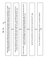
- FIG. 1 is a top view of two paddles utilized to form a superconducting qubit on a substrate according to an embodiment
- FIG. 2 is a top view of a conductive, sacrificial shorting strap formed to connect the two paddles according to an embodiment
- FIG. 3 is a top view representing fabrication of the superconducting tunnel junction on the substrate according to an embodiment
- FIG. 4 is a cross-sectional view of superconducting tunnel junction according to an embodiment
- FIG. 5A is a cross-sectional view of a first portion of a 3D quantum cavity with the substrate mounted to the cavity according to an embodiment
- FIG. 5B is a cross-sectional view of the second portion of the 3D quantum cavity according to an embodiment
- FIG. 6 is a conceptual view of a vacuum chamber for removing the sacrificial shorting strap according to an embodiment
- FIG. 7 is a top view of the substrate after removing the sacrificial shorting strap according to an embodiment
- FIG. 8 is a top view illustrating that raised portions of the two paddles may remain at the locations in which the shorting strap previously contacted the paddles according to an embodiment
- FIG. 9 is a top view illustrating that remnants of the removed shorting strap remains according to an embodiment
- FIG. 10 is a conceptual view of a cooling chamber housing the complete 3D cavity according to an embodiment
- FIGS. 11A and 11B together illustrate a method of providing a sacrificial shorting strap for protecting the tunnel junction of a superconducting qubit according to an embodiment
- FIG. 12 is a simplified version of cutting the sacrificial shorting strap in two.
- Three-dimensional (3D) superconductor qubits suffer from electrostatic discharge effects, due to the antenna effect of its two large paddles, each of which is attached to opposite sides of a delicate tunnel junction.
- Embodiments present the use of sacrificial shorting straps (e.g., niobium (Nb), which can be removed using a vapor etchant (e.g., XeF 2 ) or a wet etchant after processing and device mounting are completely finished.
- a vapor etchant e.g., XeF 2
- a wet etchant e.g., XeF 2
- a wet etchant e.g., XeF 2
- a process for fabricating 3D superconducting qubits is to make aluminum (Al) paddles and Al/AlO x /Al tunnel junctions on a sapphire substrate. In such a device, all components are resilient to XeF 2 etching according to an embodiment.
- the technique teaches the fabrication of a niobium (or other conductive material which can be etched by XeF 2 or other vapor etchant) shorting strap before the fabrication of the Al/AlO x /Al tunnel junction. Forming the sacrificial shorting strap can be either before or after paddle formation. After junction fabrication, dicing, and mounting, the sacrificial shorting strap is then removed using XeF 2 .
- FIG. 1 is a top view according to an embodiment.
- FIG. 1 illustrates a substrate 100 with two paddles 5 A and 5 B according to an embodiment.
- the substrate 100 may be, e.g., silicon, germanium, sapphire, etc.
- a conductive layer may be deposited on top of the substrate 100 , and the two paddles (pads) 5 A and 5 B are etched from the conductive layer.
- the two paddles 5 A and 5 B may be made of a superconductive material, such as aluminum, titanium nitride, niobium, and/or niobium nitride.
- Superconductivity is the phenomenon wherein the electrical resistance of a metal disappears when the metal is cooled. Superconductivity occurs in a variety of metals, but only when they are cooled to extremely low temperatures, e.g., near absolute zero.
- FIG. 2 is a top view according to an embodiment.
- FIG. 2 illustrates that a conductive (sacrificial) shorting strap 10 is formed to electrically connect paddles 5 A and 5 B.
- One end of the conductive shorting strap 10 touches and/or is on top of the paddle 5 A.
- the other end of the conductive shorting strap 10 touches and/or is on top of the paddle 5 B.
- the conductive shorting strap 10 is an electrical shunt for electrostatic discharge while providing a path to bypass the path of the delicate tunnel junction (e.g., tunnel junction 40 shown in FIG. 3 ).
- the shorting strap 10 may be formed by depositing the conductive material and etching to the desired shape.
- the conductive shorting strap 10 is made of a material that is highly selectable for etching by an etchant while not etching other material as discussed further herein.
- the shorting strap 10 may be a superconducting material such as, e.g., niobium (Nb), aluminum (Al), titanium nitride (TiN), niobium boride (NbB), where the strap material can be etched selectively (compared) to other layers on the substrate 100 .
- a superconducting strap residue that is not completely removed would not be lossy.
- the shorting strap 10 may be a material that is not superconducting but at least mildly conductive, such as, e.g., copper (Cu), silicon (Si), amorphous Si, or a conductive polymer, where the strap material can be etched selectively (compared) to other layers on the substrate 100 and which can be removed cleanly without residue.
- Cu copper
- Si silicon
- amorphous Si or a conductive polymer
- the substrate 100 is not silicon, e.g., the substrate 100 may be sapphire, the shorting strap 10 may be silicon, and the etchant is configured to select silicon while not selecting the other layers on the substrate 100 .
- FIG. 3 is a top view representing fabrication of the superconducting tunnel junction 40 on the substrate 100 .
- the superconducting tunnel junction 40 is connected to the paddles 5 A and 5 B via electrodes 20 A and 20 B.
- the electrode 20 A of the tunnel junction 40 is connected to and touching paddle 5 A, while the electrode 20 B of the tunnel junction 40 is connected to and touching paddle 5 B.
- the process of fabricating the superconducting tunnel junction 40 is understood by one skilled in the art.
- the superconducting tunnel junction (STJ), also known as a superconductor-insulator-superconductor tunnel junction (SIS), is an electronic device consisting of two superconductors separated by a very thin layer of insulating material. Current passes through the junction via the process of quantum tunneling.
- the STJ is a type of Josephson junction and is part of the qubit.
- FIG. 4 is a cross-sectional view of the tunnel junction 40 according to an embodiment.
- FIG. 4 shows the electrodes 20 A and 20 B sandwiching a thin insulator layer 25 .
- the electrodes 20 A and 20 B may be made of a superconducting material, such as aluminum (Al), titanium nitride (TiN), niobium (Nb), and/or niobium nitride (NbN). In one implementation, the electrodes 20 A and 20 B may be made of the same superconducting material of the paddles 5 A and 5 B.
- the insulator layer 25 may be an oxide such as, e.g., aluminum oxide (AlO) and/or silicon nitride (SiN).
- the thickness (in the z-axis) of the electrodes 20 A and 20 B may be 50 nanometers (nm) to 500 nm.
- the thickness of the insulator layer 25 is such that, when separating the two superconducting electrodes 20 A and 20 B, the insulator layer 25 is thin enough so that electrons can quantum-mechanically tunnel through the barrier, as understood by one skilled in the art.
- three-dimensional (3D) superconductor tunnel junction 40 can suffer from electrostatic discharge effects, due to the antenna effect of the two large paddles 5 A and 5 B, each of which is attached to opposite sides of the delicate tunnel junction 40 via the electrodes 20 A and 20 B.
- the shorting strap 10 has a lower resistance than the superconducting tunnel junction 40 thus allowing the shorting strap 10 to act as an electrical shunt whenever electrostatic energy is discharged between the paddles 5 A and 5 B, all while avoiding electrostatic discharge through the high resistance tunnel junction 40 . Accordingly, the substrate 100 can be physically handled by an operator without blowing the insulator 25 , because the electrostatic discharge flows through the conductive shorting strap 10 instead.
- Blowing the insulator layer 25 denotes forming holes in the insulator layer 25 , thus preventing the insulator layer 25 from performing as an insulator layer 25 . It is noted that the shorting strap 10 is not required to be a highly conductive material, as long as the shorting strap 10 has a lower resistance than the tunnel junction 40 .
- FIG. 5A illustrates a first portion 505 A of the 3D cavity
- FIG. 5B illustrates a second portion 505 B of the 3D cavity.
- the first and second portions 505 A and 505 B are each one-half of the 3D cavity, and both halves are attached together to form the 3D cavity (enclosure) as understood by one skilled in the art.
- the first and second portions 505 A and 505 B may be attached together with screws, clamps, and/or any other attaching device for microwave cavities as understood by one skilled in the art. This is one example of a 3D cavity and one skilled in the art understands that there are other types of 3D cavities.
- the 3D cavity may also be referred to as a quantum cavity, microwave cavity, waveguide enclosure, etc., for controlling the frequency of the circuit on the substrate 100 .
- the combined portions 505 A and 505 B may be an enclosed box of a few centimeters or inches in length, width, and depth.
- FIG. 5A shows the first portion 505 A (e.g., one half) of the 3D cavity with an input port 510 A and an output port 510 B for inputting and outputting microwave signals to/from the substrate 100 .
- the input port 510 A and the output port 510 B may be female inputs for attaching coaxial cables.
- the substrate 100 (with the layers forming a circuit) may be considered a chip or assembly that has been diced for use.
- the substrate 100 is mounted to the first portion 505 A across an elongated hole 520 A within the first portion 505 A.
- the substrate 100 may be mounted using screws or an adhesive.
- FIG. 5B shows the second portion 505 B (e.g., other half) of the 3D cavity.
- the second portion 505 B has an elongated hole 520 B that matches up with the elongated hole 520 A in the first potion 505 A, when the first and second portions 505 A and 505 B are combined.
- the substrate 100 i.e., chip
- the substrate 100 may be fixed to the second portion 505 B across the elongated hole 520 B.
- the substrate 100 may be fixed in the elongated hole 520 A or 520 B.
- the first portion 505 A and the second portion 505 B are made of the same material.
- the first and second portions 505 A and 505 B of the 3D cavity are made of copper, for example.
- FIG. 6 is a conceptual view of a vacuum chamber 600 for deposition of material and etching material.
- the vacuum chamber 600 includes one or more inputs for inputting chemicals/materials and an output for evacuating chemicals/materials.
- the first portion 505 A containing the substrate 100 is placed in the vacuum chamber 600 .
- the details of the substrate 100 are not shown for conciseness in FIGS. 5A, 5B, and 6 , but it is understood that the substrate 100 includes the two large paddles 5 A and 5 B, the electrode 20 A and 20 B, the tunnel junction 40 , and the shorting strap 10 (along with a readout resonator (not shown) as understood by one skilled in the art).
- an etchant 605 may be applied to the substrate 100 mounted to the first portion 505 A within the vacuum chamber 600 .
- the purpose of the etchant 605 is to etch (i.e., remove) the conductive shorting strap 10 while not affecting the substrate 100 , the two large paddles 5 A and 5 B, the electrode 20 A and 20 B, and the tunnel junction 40 (along with the readout resonator (not shown)).
- the conductive shorting strap 10 is completely removed from the substrate 100 while the substrate 100 is mounted to the first portion 505 A.
- the first portion 505 A now serving as an alternative path to the tunnel junction 40 , is able to discharge any electrostatic electricity, and thus protects the tunnel junction 40 while the shorting strap 10 is removed. Therefore, the substrate 100 mounted to the first portion 505 A can be physically handled by the operator without risk of electrostatic discharge that would normally damage the tunnel junction 40 .
- the etchant 605 may be a vapor etchant such as, e.g., XeF 2 .
- the conductive shorting strap 10 may be niobium, tantalum, and/or silicon, and the XeF 2 removes niobium (tantalum or silicon) conductive shorting strap 10 , without etching the other layers on the substrate 100 .
- the etchant 605 may be a wet etchant whose purpose is to remove the conductive shorting strap 10 without etching the other layers.
- an organic solvent may be used to remove a conducting polymer as the conductive shorting strap 10 without etching the other layers on the substrate 100 .
- FIG. 7 illustrates the substrate 100 after being removed from the vacuum chamber 600 and after being processed by the etchant 605 .
- the substrate 100 is still mounted on the first portion 505 A of the 3D cavity but the first portion 505 A is not shown for clarity.
- FIG. 7 shows that the conductive shorting strap 10 has been removed.
- the tunnel junction 40 remains protected from electrostatic discharge because of being mounted to the first portion 505 A of the 3D cavity.
- FIG. 8 is a top view illustrating that raised portions 805 A and 805 B of paddles 5 A and 5 B may remain at the locations in which the conductive shorting strap 10 previously contacted the paddles 5 A and 5 B.
- the raised portions 805 A and 805 B may be a result of areas in the substrate 100 that did not endure the effects of lithography processing performed after the shorting strap 10 were deposited. Fabrication processing of subsequent layers on the substrate 100 bombards the previously formed paddles 5 A and 5 B, and this bombardment of physical and chemical processing may reduce the thickness of the paddles 5 A and 5 B in the z-axis.
- the raised portions 805 A and 805 B were covered (i.e., protected) by the shorting straps 10 during the bombardment, and thus the raised portions 805 A and 805 B are not worn away as compared to areas of the paddles 5 A and 5 B that were uncovered.
- the raised portions 805 A and 805 B are the actual material of the paddles 5 A and 5 B but at a higher height in the z-axis.
- the tunnel junction 40 and electrodes 20 A and 20 B are fabricated subsequent to the shorting strap 10 . Additionally, fabrication of the readout resonator (not shown) may be subsequent to fabricating the shorting strap 10 .
- FIG. 9 illustrates locations 905 A and 905 B on the paddles 5 A and 5 B that contain remnants 10 A and 10 B of the shorting strap 10 itself according to an embodiment.
- the locations 905 A and 905 B are the places at which the shorting strap 10 contacted and covered the paddles 5 A and 5 B.
- the remnants 10 A and 10 B of the shorting strap 10 were not completely removed during the etching process by the etchant 605 , and thus remain on the paddles 5 A and 5 B.
- the material of the remnants 10 A and 10 B are the same material of the removed shorting strap 10 .
- FIG. 10 is a conceptual view of a cooling chamber 1000 .
- the first and second portions 505 A and 505 B are combined together to form the complete 3D cavity (also referred to as a quantum cavity).
- the substrate 100 is still mounted on the first portion 505 A within the 3D cavity.
- the 3D cavity (the enclosure formed by first and second portions 505 A and 505 B) is placed into the cooling chamber 1000 for operation and testing as understood by one skilled in the art.
- the cooling chamber 1000 represents a cryogenic chamber as understood by one skilled in the art.
- FIGS. 11A and 11B are a method 1100 of providing a sacrificial shorting strap 10 for protecting the tunnel junction 40 of a superconducting qubit according to an embodiment. Reference can be made to FIGS. 1-10 .
- the first electrode paddle 5 A and the second electrode paddle 5 B are formed on the substrate 100 , where the first electrode paddle 5 A and the second electrode paddle 5 B oppose one another, as depicted in FIG. 1 .
- the sacrificial shorting strap 10 is formed on the substrate 100 and the parts of the paddles 5 A, 5 B, and the sacrificial shorting strap 10 electrically connects the first electrode paddle 5 A and the second electrode paddle 5 B, as depicted in FIG. 2 .
- the tunnel junction 40 is formed to electrically connect the first electrode paddle 5 A and the second electrode paddle 5 B, after forming the sacrificial shorting strap 10 .
- the tunnel junction 40 has electrodes 20 A and 20 B and insulator 25 , as depicted in FIGS. 3 and 4 .
- the substrate 100 e.g., a wafer diced into a chip
- the substrate 100 is mounted the on a portion (e.g., the first portion 505 A and/or the second portion 505 B) of a quantum cavity, as depicted in FIGS. 5A and 5B .
- the portion (e.g., first portion 505 A and/or 505 B) of the quantum cavity is placed in a vacuum chamber 600 , as depicted in FIG. 6 .
- the sacrificial shorting strap 10 is etched away in the vacuum chamber 600 while the substrate is mounted to the portion (e.g., first portion 505 A and/or 505 B) of the quantum cavity, such that the sacrificial shorting strap 10 no longer connects the first electrode paddle 5 A and the second electrode paddle 5 B.
- the removal of the sacrificial shorting strap 10 is depicted in FIGS. 6 and 7 .
- the quantum cavity (combination of the first and second portions 505 A and 505 B) is placed in a cooling chamber 1000 for operation, and the tunnel junction 40 has been protected from electrostatic discharge by the now removed sacrificial shorting strap 10 , as depicted in FIG. 10 .
- an etchant 605 is utilized to etch away the sacrificial shorting strap 10 without removing the tunnel junction 40 , the first electrode paddle 5 A, and the second electrode paddle 5 B.
- the etchant is a wet etchant that does not attack the tunnel junction 40 , the first electrode paddle 5 A, and the second electrode paddle 5 B.
- the etchant 605 is a dry etchant that does not attack the tunnel junction 40 , the first electrode paddle 5 A, and the second electrode paddle 5 B.
- the dry etchant is XeF 2 , for example.
- an etchant 605 is utilized to etch away the sacrificial shorting strap, without requiring the sacrificial shorting strap 10 to be cut in order sever the sacrificial shorting strap, as depicted in FIG. 12 .
- an etchant 605 is utilized to etch away the sacrificial shorting strap 10 , without leaving the sacrificial shorting strap 10 severed into a first part and a second part opposing each other, as depicted in FIG. 12 .
- FIG. 12 illustrates a simplified version of cutting the sacrificial shorting strap 10 in two, while the sacrificial shorting strap 10 is mounted to the first portion 505 A (not shown in FIG. 12 ).
- the requirement to cut the sacrificial shorting strap 10 while the tunnel junction 40 (not shown in FIG. 12 ) is already in place is no longer necessary, because the sacrificial shorting strap 10 is removed by the etchant 605 .
- the tunnel junction 40 is a Josephson junction.
- the tunnel junction 40 comprises a first superconducting electrode 20 A and a second superconducting electrode 20 B, where the first superconducting electrode 20 A and the second superconducting electrode 20 B sandwich an insulator layer 25 as depicted in FIGS. 3 and 4 .
- the sacrificial shorting strap 10 prevents the insulator layer 25 in the tunnel junction from receiving the electrostatic discharge, thus protecting the insulator layer 25 from becoming defective.
- one end of the sacrificial shorting strap 10 connects at a first location on the first electrode paddle 5 A and another end of the sacrificial shorting strap 10 connects at a second location on the second electrode paddle 5 B.
- the first electrode paddle 5 A has a first raised portion 805 A at the first location and the second electrode paddle 5 B has a second raised portion 805 B at the second location, as depicted in FIG. 8 .
- the first raised portion 805 A and the second raised portion 805 B are material of the first electrode paddle 5 A and the second electrode paddle 5 B.
- the first raised portion 805 A of the material has a higher height (in the z-axis) at the first location than other areas of the material of the first electrode paddle 5 A (i.e., the other areas are not at the location of the raised portion 805 A).
- the second raised portion 805 B of the material has a higher height (in the z-axis) at the second location than other areas of the material of the second electrode paddle 5 B (i.e., the other areas are not at the location of the second raised portion 805 B).
- the one end and another end of the sacrificial shorting strap 10 covered the first location and the second location during formation of the tunnel junction 40 , thus keeping the material at the first location and the second location from wearing away resulting in the first raised portion 805 A and the second raised portion 805 B.
- the first location includes a residual portion 10 A of the sacrificial shorting strap 10
- the second location includes another residual portion 10 B of the sacrificial shorting strap 10 as depicted in FIG. 9 .
- the residual portion 10 A and the other residual portion 10 B of the sacrificial shorting strap 10 do not overhang from the first and second electrode paddles, respectively.
- the residual portion 10 A and the another residual portion 10 B in contrast to overhanging parts of the sacrificial shorting strap 10 in FIG. 12 .
- the quantum cavity is a three-dimensional cavity for operating the tunnel junction 40 within the cooling chamber 1000 , as depicted in FIG. 10 .
- Deposition is any process that grows, coats, or otherwise transfers a material onto the wafer.
- Available technologies include physical vapor deposition (PVD), chemical vapor deposition (CVD), electrochemical deposition (ECD), molecular beam epitaxy (MBE) and more recently, atomic layer deposition (ALD) among others.
- Removal is any process that removes material from the wafer: examples include etch processes (either wet or dry), and chemical-mechanical planarization (CMP), etc.
- Patterning is the shaping or altering of deposited materials, and is generally referred to as lithography.
- the wafer is coated with a chemical called a photoresist; then, a machine called a stepper focuses, aligns, and moves a mask, exposing select portions of the wafer below to short wavelength light; the exposed regions are washed away by a developer solution. After etching or other processing, the remaining photoresist is removed.
- Patterning also includes electron-beam lithography.
- Modification of electrical properties may include doping, such as doping transistor sources and drains, generally by diffusion and/or by ion implantation. These doping processes are followed by furnace annealing or by rapid thermal annealing (RTA). Annealing serves to activate the implanted dopants.
- doping such as doping transistor sources and drains
- RTA rapid thermal annealing
- each block in the flowchart or block diagrams may represent a module, segment, or portion of instructions, which comprises one or more executable instructions for implementing the specified logical function(s).
- the functions noted in the block may occur out of the order noted in the figures.
- two blocks shown in succession may, in fact, be executed substantially concurrently, or the blocks may sometimes be executed in the reverse order, depending upon the functionality involved.
Abstract
A technique relates to protecting a tunnel junction. A first electrode paddle and a second electrode paddle are on a substrate. The first and second electrode paddles oppose one another. A sacrificial shorting strap is formed on the substrate. The sacrificial shorting strap connects the first electrode paddle and the second electrode paddle; The tunnel junction is formed connecting the first electrode paddle and the second electrode paddle, after forming the sacrificial shorting strap. The substrate is mounted on a portion of a quantum cavity. The portion of the quantum cavity is placed in a vacuum chamber. The sacrificial shorting strap is etched away in the vacuum chamber while the substrate is mounted to the portion of the quantum cavity, such that the sacrificial shorting strap no longer connects the first and second electrode paddles. The tunnel junction has been protected from electrostatic discharge by the sacrificial shorting strap.
Description
This invention was made with Government support under Contract No.: W911NF-10-1-0324 awarded by the Intelligence Advanced Research Projects Activity. The Government has certain rights to this invention.
The present invention relates to superconducting techniques, and more specifically, to a sacrificial shorting strap for superconducting qubits.
Quantum computing employs resonant structures called qubits to store information, and resonators (e.g., as a two-dimensional (2D) planar waveguide or as a three-dimensional (3D) microwave cavity) to read out and manipulate the qubits. To date, a major focus has been on improving lifetimes of the qubits in order to allow calculations (i.e., manipulation and readout) to take place before the information is lost to decoherence of the qubits. Currently, qubit coherence times can be as high as 100 microseconds and efforts are being made to increase the coherence times. One area of research with respect to increasing coherence times is focused on eliminating material at the edges of the qubit (i.e., edges) in order to reduce the electric field in that area. The material in proximity to the qubit includes imperfections that support defects known as two-level systems (TLS).
According to one embodiment, a method of forming a protected tunnel junction is provided. The method includes forming a first electrode paddle and a second electrode paddle on a substrate, where the first electrode paddle and the second electrode paddle oppose one another, and forming a sacrificial shorting strap on the substrate, where the sacrificial shorting strap connects the first electrode paddle and the second electrode paddle. The method includes forming the tunnel junction connecting the first electrode paddle and the second electrode paddle, after forming the sacrificial shorting strap, mounting the substrate on a portion of a quantum cavity, and placing the portion of the quantum cavity in a vacuum chamber. Also, the method includes etching away the sacrificial shorting strap in the vacuum chamber while the substrate is mounted to the portion of the quantum cavity, such that the sacrificial shorting strap no longer connects the first electrode paddle and the second electrode paddle, and placing the quantum cavity in a cooling chamber for operation. The tunnel junction has been protected from electrostatic discharge by the sacrificial shorting strap.
According to one embodiment, a system for protecting a tunnel junction from electrostatic discharge when handling the tunnel junction. The system includes a quantum cavity configured as a waveguide enclosure, and an assembly mounted to the quantum cavity. The assembly includes a first electrode paddle and a second electrode paddle on a substrate, where the first electrode paddle and the second electrode paddle oppose one another. Also, the assembly includes the tunnel junction connecting the first electrode paddle and the second electrode paddle, a first location on the first electrode paddle, and a second location on the second electrode paddle. The first electrode paddle has a first raised portion at the first location and the second electrode paddle has a second raised portion at the second location. The first raised portion corresponds to one end of a sacrificial shorting strap previously connected at the first location on the first electrode paddle. The second raised portion corresponds to another end of the sacrificial shorting strap previously connected at the second location on the second electrode paddle.
Additional features and advantages are realized through the techniques of the present invention. Other embodiments and aspects of the invention are described in detail herein and are considered a part of the claimed invention. For a better understanding of the invention with the advantages and the features, refer to the description and to the drawings.
The subject matter which is regarded as the invention is particularly pointed out and distinctly claimed in the claims at the conclusion of the specification. The forgoing and other features, and advantages of the invention are apparent from the following detailed description taken in conjunction with the accompanying drawings in which:
Three-dimensional (3D) superconductor qubits suffer from electrostatic discharge effects, due to the antenna effect of its two large paddles, each of which is attached to opposite sides of a delicate tunnel junction.
State-of-the-art solutions include the use of a shorting strap which is manually cut through immediately before testing, leaving one end of the severed shorting strap attached to the one large paddle and the other end of the severed shorting strap attached to the other large paddle. However, this process is not scalable and introduces particulates and lossy features into the qubit system. Particles of the cut shorting strap are spewed onto and left on the two large paddles even in proximity to the delicate tunnel junction. Other lossy features incurred in this process include damage to the underlying substrate and residue left from the severing process.
Embodiments present the use of sacrificial shorting straps (e.g., niobium (Nb), which can be removed using a vapor etchant (e.g., XeF2) or a wet etchant after processing and device mounting are completely finished. This eliminates the extraneous capacitance caused by the remnant shorting strap features (i.e., particles and/or severed shorting straps attached to the two large paddles). As one example, a process for fabricating 3D superconducting qubits is to make aluminum (Al) paddles and Al/AlOx/Al tunnel junctions on a sapphire substrate. In such a device, all components are resilient to XeF2 etching according to an embodiment.
According to embodiments, the technique teaches the fabrication of a niobium (or other conductive material which can be etched by XeF2 or other vapor etchant) shorting strap before the fabrication of the Al/AlOx/Al tunnel junction. Forming the sacrificial shorting strap can be either before or after paddle formation. After junction fabrication, dicing, and mounting, the sacrificial shorting strap is then removed using XeF2.
A conductive layer may be deposited on top of the substrate 100, and the two paddles (pads) 5A and 5B are etched from the conductive layer. The two paddles 5A and 5B may be made of a superconductive material, such as aluminum, titanium nitride, niobium, and/or niobium nitride.
Superconductivity is the phenomenon wherein the electrical resistance of a metal disappears when the metal is cooled. Superconductivity occurs in a variety of metals, but only when they are cooled to extremely low temperatures, e.g., near absolute zero.
The conductive shorting strap 10 is made of a material that is highly selectable for etching by an etchant while not etching other material as discussed further herein. In one implementation, the shorting strap 10 may be a superconducting material such as, e.g., niobium (Nb), aluminum (Al), titanium nitride (TiN), niobium boride (NbB), where the strap material can be etched selectively (compared) to other layers on the substrate 100. In the case of a superconducting strap, residue that is not completely removed would not be lossy. In another implementation, the shorting strap 10 may be a material that is not superconducting but at least mildly conductive, such as, e.g., copper (Cu), silicon (Si), amorphous Si, or a conductive polymer, where the strap material can be etched selectively (compared) to other layers on the substrate 100 and which can be removed cleanly without residue.
As one example, when the substrate 100 is not silicon, e.g., the substrate 100 may be sapphire, the shorting strap 10 may be silicon, and the etchant is configured to select silicon while not selecting the other layers on the substrate 100.
The process of fabricating the superconducting tunnel junction 40 is understood by one skilled in the art. The superconducting tunnel junction (STJ), also known as a superconductor-insulator-superconductor tunnel junction (SIS), is an electronic device consisting of two superconductors separated by a very thin layer of insulating material. Current passes through the junction via the process of quantum tunneling. The STJ is a type of Josephson junction and is part of the qubit. As an example, FIG. 4 is a cross-sectional view of the tunnel junction 40 according to an embodiment. FIG. 4 shows the electrodes 20A and 20B sandwiching a thin insulator layer 25. The electrodes 20A and 20B may be made of a superconducting material, such as aluminum (Al), titanium nitride (TiN), niobium (Nb), and/or niobium nitride (NbN). In one implementation, the electrodes 20A and 20B may be made of the same superconducting material of the paddles 5A and 5B. The insulator layer 25 may be an oxide such as, e.g., aluminum oxide (AlO) and/or silicon nitride (SiN).
The thickness (in the z-axis) of the electrodes 20A and 20B may be 50 nanometers (nm) to 500 nm. The thickness of the insulator layer 25 is such that, when separating the two superconducting electrodes 20A and 20B, the insulator layer 25 is thin enough so that electrons can quantum-mechanically tunnel through the barrier, as understood by one skilled in the art.
As noted above, three-dimensional (3D) superconductor tunnel junction 40 can suffer from electrostatic discharge effects, due to the antenna effect of the two large paddles 5A and 5B, each of which is attached to opposite sides of the delicate tunnel junction 40 via the electrodes 20A and 20B. However, the shorting strap 10 has a lower resistance than the superconducting tunnel junction 40 thus allowing the shorting strap 10 to act as an electrical shunt whenever electrostatic energy is discharged between the paddles 5A and 5B, all while avoiding electrostatic discharge through the high resistance tunnel junction 40. Accordingly, the substrate 100 can be physically handled by an operator without blowing the insulator 25, because the electrostatic discharge flows through the conductive shorting strap 10 instead. Blowing the insulator layer 25 denotes forming holes in the insulator layer 25, thus preventing the insulator layer 25 from performing as an insulator layer 25. It is noted that the shorting strap 10 is not required to be a highly conductive material, as long as the shorting strap 10 has a lower resistance than the tunnel junction 40.
The first portion 505A and the second portion 505B are made of the same material. The first and second portions 505A and 505B of the 3D cavity are made of copper, for example.
According to an embodiment, the first portion 505A containing the substrate 100 is placed in the vacuum chamber 600. The details of the substrate 100 are not shown for conciseness in FIGS. 5A, 5B, and 6 , but it is understood that the substrate 100 includes the two large paddles 5A and 5B, the electrode 20A and 20B, the tunnel junction 40, and the shorting strap 10 (along with a readout resonator (not shown) as understood by one skilled in the art).
In FIG. 6 , an etchant 605 may be applied to the substrate 100 mounted to the first portion 505A within the vacuum chamber 600. The purpose of the etchant 605 is to etch (i.e., remove) the conductive shorting strap 10 while not affecting the substrate 100, the two large paddles 5A and 5B, the electrode 20A and 20B, and the tunnel junction 40 (along with the readout resonator (not shown)). The conductive shorting strap 10 is completely removed from the substrate 100 while the substrate 100 is mounted to the first portion 505A. The first portion 505A, now serving as an alternative path to the tunnel junction 40, is able to discharge any electrostatic electricity, and thus protects the tunnel junction 40 while the shorting strap 10 is removed. Therefore, the substrate 100 mounted to the first portion 505A can be physically handled by the operator without risk of electrostatic discharge that would normally damage the tunnel junction 40.
In one implementation, the etchant 605 may be a vapor etchant such as, e.g., XeF2. In this case, the conductive shorting strap 10 may be niobium, tantalum, and/or silicon, and the XeF2 removes niobium (tantalum or silicon) conductive shorting strap 10, without etching the other layers on the substrate 100.
In another implementation, the etchant 605 may be a wet etchant whose purpose is to remove the conductive shorting strap 10 without etching the other layers. For example, an organic solvent may be used to remove a conducting polymer as the conductive shorting strap 10 without etching the other layers on the substrate 100.
According to an embodiment, FIG. 7 illustrates the substrate 100 after being removed from the vacuum chamber 600 and after being processed by the etchant 605. At this point, the substrate 100 is still mounted on the first portion 505A of the 3D cavity but the first portion 505A is not shown for clarity. FIG. 7 shows that the conductive shorting strap 10 has been removed. However, the tunnel junction 40 remains protected from electrostatic discharge because of being mounted to the first portion 505A of the 3D cavity.
According to another embodiment, FIG. 8 is a top view illustrating that raised portions 805A and 805B of paddles 5A and 5B may remain at the locations in which the conductive shorting strap 10 previously contacted the paddles 5A and 5B. The raised portions 805A and 805B may be a result of areas in the substrate 100 that did not endure the effects of lithography processing performed after the shorting strap 10 were deposited. Fabrication processing of subsequent layers on the substrate 100 bombards the previously formed paddles 5A and 5B, and this bombardment of physical and chemical processing may reduce the thickness of the paddles 5A and 5B in the z-axis. However, the raised portions 805A and 805B were covered (i.e., protected) by the shorting straps 10 during the bombardment, and thus the raised portions 805A and 805B are not worn away as compared to areas of the paddles 5A and 5B that were uncovered. In FIG. 8 , the raised portions 805A and 805B are the actual material of the paddles 5A and 5B but at a higher height in the z-axis. It is noted that the tunnel junction 40 and electrodes 20A and 20B are fabricated subsequent to the shorting strap 10. Additionally, fabrication of the readout resonator (not shown) may be subsequent to fabricating the shorting strap 10.
At block 1105, the first electrode paddle 5A and the second electrode paddle 5B are formed on the substrate 100, where the first electrode paddle 5A and the second electrode paddle 5B oppose one another, as depicted in FIG. 1 .
At block 1110, the sacrificial shorting strap 10 is formed on the substrate 100 and the parts of the paddles 5A, 5B, and the sacrificial shorting strap 10 electrically connects the first electrode paddle 5A and the second electrode paddle 5B, as depicted in FIG. 2 .
At block 1115, the tunnel junction 40 is formed to electrically connect the first electrode paddle 5A and the second electrode paddle 5B, after forming the sacrificial shorting strap 10. The tunnel junction 40 has electrodes 20A and 20B and insulator 25, as depicted in FIGS. 3 and 4 .
At block 1120, the substrate 100 (e.g., a wafer diced into a chip) is mounted the on a portion (e.g., the first portion 505A and/or the second portion 505B) of a quantum cavity, as depicted in FIGS. 5A and 5B .
At block 1125, the portion (e.g., first portion 505A and/or 505B) of the quantum cavity is placed in a vacuum chamber 600, as depicted in FIG. 6 .
At block 1130, the sacrificial shorting strap 10 is etched away in the vacuum chamber 600 while the substrate is mounted to the portion (e.g., first portion 505A and/or 505B) of the quantum cavity, such that the sacrificial shorting strap 10 no longer connects the first electrode paddle 5A and the second electrode paddle 5B. The removal of the sacrificial shorting strap 10 is depicted in FIGS. 6 and 7 .
At block 1135, the quantum cavity (combination of the first and second portions 505A and 505B) is placed in a cooling chamber 1000 for operation, and the tunnel junction 40 has been protected from electrostatic discharge by the now removed sacrificial shorting strap 10, as depicted in FIG. 10 .
When the substrate 100 is mounted on the quantum cavity in the vacuum chamber 600, an etchant 605 is utilized to etch away the sacrificial shorting strap 10 without removing the tunnel junction 40, the first electrode paddle 5A, and the second electrode paddle 5B.
The etchant is a wet etchant that does not attack the tunnel junction 40, the first electrode paddle 5A, and the second electrode paddle 5B. In another case, the etchant 605 is a dry etchant that does not attack the tunnel junction 40, the first electrode paddle 5A, and the second electrode paddle 5B. The dry etchant is XeF2, for example.
When the substrate 100 is mounted on the quantum cavity in the vacuum chamber 600, an etchant 605 is utilized to etch away the sacrificial shorting strap, without requiring the sacrificial shorting strap 10 to be cut in order sever the sacrificial shorting strap, as depicted in FIG. 12 . When the substrate is mounted on the quantum cavity in the vacuum chamber 600, an etchant 605 is utilized to etch away the sacrificial shorting strap 10, without leaving the sacrificial shorting strap 10 severed into a first part and a second part opposing each other, as depicted in FIG. 12 . FIG. 12 illustrates a simplified version of cutting the sacrificial shorting strap 10 in two, while the sacrificial shorting strap 10 is mounted to the first portion 505A (not shown in FIG. 12 ). By using the technique discussed in embodiments, the requirement to cut the sacrificial shorting strap 10 while the tunnel junction 40 (not shown in FIG. 12 ) is already in place is no longer necessary, because the sacrificial shorting strap 10 is removed by the etchant 605.
The tunnel junction 40 is a Josephson junction. The tunnel junction 40 comprises a first superconducting electrode 20A and a second superconducting electrode 20B, where the first superconducting electrode 20A and the second superconducting electrode 20B sandwich an insulator layer 25 as depicted in FIGS. 3 and 4 .
The sacrificial shorting strap 10 prevents the insulator layer 25 in the tunnel junction from receiving the electrostatic discharge, thus protecting the insulator layer 25 from becoming defective.
Before etching away the sacrificial shorting strap 10 in the vacuum chamber 600, one end of the sacrificial shorting strap 10 connects at a first location on the first electrode paddle 5A and another end of the sacrificial shorting strap 10 connects at a second location on the second electrode paddle 5B. After etching away the sacrificial shorting strap 10 in the vacuum chamber 600 while the substrate 100 is mounted to the portion of the quantum cavity, the first electrode paddle 5A has a first raised portion 805A at the first location and the second electrode paddle 5B has a second raised portion 805B at the second location, as depicted in FIG. 8 . The first raised portion 805A and the second raised portion 805B are material of the first electrode paddle 5A and the second electrode paddle 5B. The first raised portion 805A of the material has a higher height (in the z-axis) at the first location than other areas of the material of the first electrode paddle 5A (i.e., the other areas are not at the location of the raised portion 805A). The second raised portion 805B of the material has a higher height (in the z-axis) at the second location than other areas of the material of the second electrode paddle 5B (i.e., the other areas are not at the location of the second raised portion 805B). The one end and another end of the sacrificial shorting strap 10 covered the first location and the second location during formation of the tunnel junction 40, thus keeping the material at the first location and the second location from wearing away resulting in the first raised portion 805A and the second raised portion 805B.
The first location includes a residual portion 10A of the sacrificial shorting strap 10, and the second location includes another residual portion 10B of the sacrificial shorting strap 10 as depicted in FIG. 9 . The residual portion 10A and the other residual portion 10B of the sacrificial shorting strap 10 do not overhang from the first and second electrode paddles, respectively. For example, the residual portion 10A and the another residual portion 10B in contrast to overhanging parts of the sacrificial shorting strap 10 in FIG. 12 .
The quantum cavity is a three-dimensional cavity for operating the tunnel junction 40 within the cooling chamber 1000, as depicted in FIG. 10 .
It will be noted that various semiconductor device fabrication methods may be utilized to fabricate the components/elements discussed herein as understood by one skilled in the art. In semiconductor device fabrication, the various processing steps fall into four general categories: deposition, removal, patterning, and modification of electrical properties.
Deposition is any process that grows, coats, or otherwise transfers a material onto the wafer. Available technologies include physical vapor deposition (PVD), chemical vapor deposition (CVD), electrochemical deposition (ECD), molecular beam epitaxy (MBE) and more recently, atomic layer deposition (ALD) among others.
Removal is any process that removes material from the wafer: examples include etch processes (either wet or dry), and chemical-mechanical planarization (CMP), etc.
Patterning is the shaping or altering of deposited materials, and is generally referred to as lithography. For example, in conventional lithography, the wafer is coated with a chemical called a photoresist; then, a machine called a stepper focuses, aligns, and moves a mask, exposing select portions of the wafer below to short wavelength light; the exposed regions are washed away by a developer solution. After etching or other processing, the remaining photoresist is removed. Patterning also includes electron-beam lithography.
Modification of electrical properties may include doping, such as doping transistor sources and drains, generally by diffusion and/or by ion implantation. These doping processes are followed by furnace annealing or by rapid thermal annealing (RTA). Annealing serves to activate the implanted dopants.
The flowchart and block diagrams in the Figures illustrate the architecture, functionality, and operation of possible implementations of systems, methods, and computer program products according to various embodiments of the present invention. In this regard, each block in the flowchart or block diagrams may represent a module, segment, or portion of instructions, which comprises one or more executable instructions for implementing the specified logical function(s). In some alternative implementations, the functions noted in the block may occur out of the order noted in the figures. For example, two blocks shown in succession may, in fact, be executed substantially concurrently, or the blocks may sometimes be executed in the reverse order, depending upon the functionality involved. It will also be noted that each block of the block diagrams and/or flowchart illustration, and combinations of blocks in the block diagrams and/or flowchart illustration, can be implemented by special purpose hardware-based systems that perform the specified functions or acts or carry out combinations of special purpose hardware and computer instructions.
Claims (5)
1. A system for protecting a tunnel junction from electrostatic discharge when handling the tunnel junction, the system comprising:
a quantum cavity configured as a waveguide enclosure;
an assembly mounted to the quantum cavity;
wherein the assembly includes:
a first electrode paddle and a second electrode paddle both formed on an upper surface of a substrate, the first electrode paddle and the second electrode paddle opposing one another;
the tunnel junction connecting the first electrode paddle and the second electrode paddle, the tunnel junction formed on the upper surface of the substrate such that the tunnel junction, the first electrode paddle, and the second electrode paddle are in a same plane; and
a first location on the first electrode paddle and a second location on the second electrode paddle, the first electrode paddle having a first raised portion at the first location and the second electrode paddle having a second raised portion at the second location, the first and second raised portion being material of the substrate;
wherein the first raised portion corresponds to one end of a sacrificial shorting strap previously connected at the first location on the first electrode paddle; and
wherein the second raised portion corresponds to another end of the sacrificial shorting strap previously connected at the second location on the second electrode paddle.
2. The system of claim 1 , wherein the first raised portion and the second raised portion are material of the first electrode paddle and the second electrode paddle.
3. The system of claim 2 , wherein the first raised portion of the material has a higher height at the first location than other areas of the material of the first electrode paddle; and
wherein the second raised portion of the material has a higher height at the second location than other areas of the material of the second electrode paddle.
4. The system of claim 1 , wherein the first location includes a residual portion of the sacrificial shorting strap;
wherein the second location includes another residual portion of the sacrificial shorting strap; and
wherein the residual portion and the another residual portion of the sacrificial shorting strap do not overhang from the first and second electrode paddles, respectively.
5. The system of claim 4 , wherein the assembly is void of the sacrificial shorting strap such that no sacrificial shorting strap connects the first electrode paddle to the second electrode paddle.
Priority Applications (4)
| Application Number | Priority Date | Filing Date | Title |
|---|---|---|---|
| US14/714,894 US9515247B1 (en) | 2015-05-18 | 2015-05-18 | Sacrificial shorting straps for superconducting qubits |
| US14/749,157 US9705063B2 (en) | 2015-05-18 | 2015-06-24 | Sacrificial shorting straps for superconducting qubits |
| US15/349,195 US10032637B2 (en) | 2015-05-18 | 2016-11-11 | Sacrificial shorting straps for superconducting qubits |
| US15/887,297 US10256106B2 (en) | 2015-05-18 | 2018-02-02 | Sacrificial shorting straps for superconducting qubits |
Applications Claiming Priority (1)
| Application Number | Priority Date | Filing Date | Title |
|---|---|---|---|
| US14/714,894 US9515247B1 (en) | 2015-05-18 | 2015-05-18 | Sacrificial shorting straps for superconducting qubits |
Related Child Applications (2)
| Application Number | Title | Priority Date | Filing Date |
|---|---|---|---|
| US14/749,157 Continuation US9705063B2 (en) | 2015-05-18 | 2015-06-24 | Sacrificial shorting straps for superconducting qubits |
| US15/349,195 Continuation US10032637B2 (en) | 2015-05-18 | 2016-11-11 | Sacrificial shorting straps for superconducting qubits |
Publications (2)
| Publication Number | Publication Date |
|---|---|
| US20160343934A1 US20160343934A1 (en) | 2016-11-24 |
| US9515247B1 true US9515247B1 (en) | 2016-12-06 |
Family
ID=57325654
Family Applications (4)
| Application Number | Title | Priority Date | Filing Date |
|---|---|---|---|
| US14/714,894 Active US9515247B1 (en) | 2015-05-18 | 2015-05-18 | Sacrificial shorting straps for superconducting qubits |
| US14/749,157 Active US9705063B2 (en) | 2015-05-18 | 2015-06-24 | Sacrificial shorting straps for superconducting qubits |
| US15/349,195 Active US10032637B2 (en) | 2015-05-18 | 2016-11-11 | Sacrificial shorting straps for superconducting qubits |
| US15/887,297 Active US10256106B2 (en) | 2015-05-18 | 2018-02-02 | Sacrificial shorting straps for superconducting qubits |
Family Applications After (3)
| Application Number | Title | Priority Date | Filing Date |
|---|---|---|---|
| US14/749,157 Active US9705063B2 (en) | 2015-05-18 | 2015-06-24 | Sacrificial shorting straps for superconducting qubits |
| US15/349,195 Active US10032637B2 (en) | 2015-05-18 | 2016-11-11 | Sacrificial shorting straps for superconducting qubits |
| US15/887,297 Active US10256106B2 (en) | 2015-05-18 | 2018-02-02 | Sacrificial shorting straps for superconducting qubits |
Country Status (1)
| Country | Link |
|---|---|
| US (4) | US9515247B1 (en) |
Cited By (1)
| Publication number | Priority date | Publication date | Assignee | Title |
|---|---|---|---|---|
| US10032637B2 (en) | 2015-05-18 | 2018-07-24 | International Business Machines Corporation | Sacrificial shorting straps for superconducting qubits |
Families Citing this family (9)
| Publication number | Priority date | Publication date | Assignee | Title |
|---|---|---|---|---|
| EP3369047A1 (en) | 2015-10-29 | 2018-09-05 | Google LLC | Removing leakage in a quantum bit |
| US10380494B2 (en) * | 2017-08-04 | 2019-08-13 | International Business Machines Corporation | Josephson junctions for improved qubits |
| WO2019032115A1 (en) * | 2017-08-11 | 2019-02-14 | Intel Corporation | Qubit devices with josephson junctions connected below supporting circuitry |
| US10355193B2 (en) | 2017-11-28 | 2019-07-16 | International Business Machines Corporation | Flip chip integration on qubit chips |
| US10170681B1 (en) | 2017-11-28 | 2019-01-01 | International Business Machines Corporation | Laser annealing of qubits with structured illumination |
| US10418540B2 (en) | 2017-11-28 | 2019-09-17 | International Business Machines Corporation | Adjustment of qubit frequency through annealing |
| US10340438B2 (en) * | 2017-11-28 | 2019-07-02 | International Business Machines Corporation | Laser annealing qubits for optimized frequency allocation |
| US11895931B2 (en) | 2017-11-28 | 2024-02-06 | International Business Machines Corporation | Frequency tuning of multi-qubit systems |
| US11563162B2 (en) * | 2020-01-09 | 2023-01-24 | International Business Machines Corporation | Epitaxial Josephson junction transmon device |
Citations (8)
| Publication number | Priority date | Publication date | Assignee | Title |
|---|---|---|---|---|
| US5212147A (en) | 1991-05-15 | 1993-05-18 | Hewlett-Packard Company | Method of forming a patterned in-situ high Tc superconductive film |
| US20050107261A1 (en) * | 2003-10-23 | 2005-05-19 | Cantor Robin H. | Charge dissipative dielectric for cryogenic devices |
| US20060065622A1 (en) | 2004-09-27 | 2006-03-30 | Floyd Philip D | Method and system for xenon fluoride etching with enhanced efficiency |
| US20110089405A1 (en) * | 2009-02-27 | 2011-04-21 | D-Wave Systems Inc. | Systems and methods for fabrication of superconducting integrated circuits |
| US8437818B1 (en) | 2010-01-08 | 2013-05-07 | Hypres, Inc. | System and method for providing multi-conductive layer metallic interconnects for superconducting integrated circuits |
| US20130119351A1 (en) * | 2011-11-11 | 2013-05-16 | Patrick B. Shea | Quantum bits and method of forming the same |
| US20140113828A1 (en) * | 2011-03-30 | 2014-04-24 | Ambature Inc. | Electrical, mechanical, computing/ and/or other devices formed of extremely low resistance materials |
| US20140246652A1 (en) * | 2013-03-04 | 2014-09-04 | International Business Machines Corporation | Planar qubits having increased coherence times |
Family Cites Families (2)
| Publication number | Priority date | Publication date | Assignee | Title |
|---|---|---|---|---|
| US9177814B2 (en) | 2013-03-15 | 2015-11-03 | International Business Machines Corporation | Suspended superconducting qubits |
| US9515247B1 (en) | 2015-05-18 | 2016-12-06 | International Business Machines Corporation | Sacrificial shorting straps for superconducting qubits |
-
2015
- 2015-05-18 US US14/714,894 patent/US9515247B1/en active Active
- 2015-06-24 US US14/749,157 patent/US9705063B2/en active Active
-
2016
- 2016-11-11 US US15/349,195 patent/US10032637B2/en active Active
-
2018
- 2018-02-02 US US15/887,297 patent/US10256106B2/en active Active
Patent Citations (8)
| Publication number | Priority date | Publication date | Assignee | Title |
|---|---|---|---|---|
| US5212147A (en) | 1991-05-15 | 1993-05-18 | Hewlett-Packard Company | Method of forming a patterned in-situ high Tc superconductive film |
| US20050107261A1 (en) * | 2003-10-23 | 2005-05-19 | Cantor Robin H. | Charge dissipative dielectric for cryogenic devices |
| US20060065622A1 (en) | 2004-09-27 | 2006-03-30 | Floyd Philip D | Method and system for xenon fluoride etching with enhanced efficiency |
| US20110089405A1 (en) * | 2009-02-27 | 2011-04-21 | D-Wave Systems Inc. | Systems and methods for fabrication of superconducting integrated circuits |
| US8437818B1 (en) | 2010-01-08 | 2013-05-07 | Hypres, Inc. | System and method for providing multi-conductive layer metallic interconnects for superconducting integrated circuits |
| US20140113828A1 (en) * | 2011-03-30 | 2014-04-24 | Ambature Inc. | Electrical, mechanical, computing/ and/or other devices formed of extremely low resistance materials |
| US20130119351A1 (en) * | 2011-11-11 | 2013-05-16 | Patrick B. Shea | Quantum bits and method of forming the same |
| US20140246652A1 (en) * | 2013-03-04 | 2014-09-04 | International Business Machines Corporation | Planar qubits having increased coherence times |
Non-Patent Citations (13)
| Title |
|---|
| C. Rigetti et al., "Superconducting qubit in a waveguide cavity with a coherence time approaching 0.1 ms.," Physical Review B, vol. 86, No. 10, 2012, 100506, 5 pages. |
| J. B. Chang et al., "Suspended Superconducting Qubits," U.S. Appl. No. 13/834,291, filed Mar. 15, 2013. |
| J. B. Chang et al., "Suspended Superconducting Qubits," U.S. Appl. No. 13/969,776, filed Aug. 19, 2013. |
| J. M. Martinis, "Superconducting phase qubits." Quantum Information Processing, vol. 8, No. 2-3, 2009, pp. 81-103. |
| Josephine B. Chang, et al.; "Sacrificial Shorting Straps for Superconducting Qubits"; U.S. Appl. No. 14/749,157, filed Jun. 24, 2015. |
| Josephine B. Chang, et al.; "Suspended Superconducting Qubits"; U.S. Appl. No. 13/834,291, filed Mar. 15, 2013. |
| Josephine B. Chang, et al.; "Suspended Superconducting Qubits"; U.S. Appl. No. 13/969,776, filed Aug. 19, 2013. |
| Josephine B. Chang, et al.; "Suspended Superconducting Qubits"; U.S. Appl. No. 14/812,446, filed Jul. 29, 2015. |
| List of IBM Patents or Patent Applications Treated as Related; May 20, 2015; pp. 1-2. |
| List of IBM Patents or Patent Applications Treated As Related-Date Filed: Aug. 31, 2015; 1 page. |
| R. Bialczak, "Development of the Fundamental Components of a Superconducting Qubit Quantum Computer," PhD Dissertation, University of California, Santa Barbara, 2011. |
| S. Yao et al., "SiN-based micro cantilever actuators using NdFeB/Ta permanent magnetic thin film." 4th IEEE International Conference on Nano/Micro Engineered and Molecular Systems, 2009. NEMS 2009, pp. 416-419. |
| X. L. Fu et al., "Gas-assisted etching of niobium with focused ion beam," Microelectronic Engineering, vol. 78, 2005, pp. 29-33. |
Cited By (2)
| Publication number | Priority date | Publication date | Assignee | Title |
|---|---|---|---|---|
| US10032637B2 (en) | 2015-05-18 | 2018-07-24 | International Business Machines Corporation | Sacrificial shorting straps for superconducting qubits |
| US10256106B2 (en) | 2015-05-18 | 2019-04-09 | International Business Machines Corporation | Sacrificial shorting straps for superconducting qubits |
Also Published As
| Publication number | Publication date |
|---|---|
| US10032637B2 (en) | 2018-07-24 |
| US9705063B2 (en) | 2017-07-11 |
| US10256106B2 (en) | 2019-04-09 |
| US20160343934A1 (en) | 2016-11-24 |
| US20180174852A1 (en) | 2018-06-21 |
| US20160343935A1 (en) | 2016-11-24 |
| US20170062228A1 (en) | 2017-03-02 |
Similar Documents
| Publication | Publication Date | Title |
|---|---|---|
| US10256106B2 (en) | Sacrificial shorting straps for superconducting qubits | |
| US11380974B2 (en) | Superconducting airbridge crossover using superconducting sacrificial material | |
| US11133452B2 (en) | Trilayer Josephson junction structure with small air bridge and no interlevel dielectric for superconducting qubits | |
| US10424712B2 (en) | Methods for making a superconducting device with at least one enclosure | |
| EP3703141B1 (en) | Capping layer for reducing ion mill damage | |
| CA2898598C (en) | Superconducting device with at least one enclosure | |
| JP7185980B2 (en) | Superconducting qubits with Josephson junctions for improved qubits, methods of fabricating superconducting qubits, and methods of forming microwave devices | |
| WO2018065833A1 (en) | Superconducting electronic integrated circuit |
Legal Events
| Date | Code | Title | Description |
|---|---|---|---|
| AS | Assignment |
Owner name: INTERNATIONAL BUSINESS MACHINES CORPORATION, NEW Y Free format text: ASSIGNMENT OF ASSIGNORS INTEREST;ASSIGNORS:CHANG, JOSEPHINE B.;MCCLURE, DOUGLAS T., III;REEL/FRAME:035660/0740 Effective date: 20150515 |
|
| STCF | Information on status: patent grant |
Free format text: PATENTED CASE |
|
| MAFP | Maintenance fee payment |
Free format text: PAYMENT OF MAINTENANCE FEE, 4TH YEAR, LARGE ENTITY (ORIGINAL EVENT CODE: M1551); ENTITY STATUS OF PATENT OWNER: LARGE ENTITY Year of fee payment: 4 |