US9508688B2 - Semiconductor packages with interposers and methods of manufacturing the same - Google Patents

Semiconductor packages with interposers and methods of manufacturing the same Download PDF

Info

Publication number
US9508688B2
US9508688B2 US14/850,283 US201514850283A US9508688B2 US 9508688 B2 US9508688 B2 US 9508688B2 US 201514850283 A US201514850283 A US 201514850283A US 9508688 B2 US9508688 B2 US 9508688B2
Authority
US
United States
Prior art keywords
semiconductor chip
connectors
interposer
semiconductor
group
Prior art date
Legal status (The legal status is an assumption and is not a legal conclusion. Google has not performed a legal analysis and makes no representation as to the accuracy of the status listed.)
Active
Application number
US14/850,283
Other versions
US20160300815A1 (en
Inventor
Jong Hoon Kim
Current Assignee (The listed assignees may be inaccurate. Google has not performed a legal analysis and makes no representation or warranty as to the accuracy of the list.)
SK Hynix Inc
Original Assignee
SK Hynix Inc
Priority date (The priority date is an assumption and is not a legal conclusion. Google has not performed a legal analysis and makes no representation as to the accuracy of the date listed.)
Filing date
Publication date
Application filed by SK Hynix Inc filed Critical SK Hynix Inc
Assigned to SK Hynix Inc. reassignment SK Hynix Inc. ASSIGNMENT OF ASSIGNORS INTEREST (SEE DOCUMENT FOR DETAILS). Assignors: KIM, JONG HOON
Publication of US20160300815A1 publication Critical patent/US20160300815A1/en
Application granted granted Critical
Publication of US9508688B2 publication Critical patent/US9508688B2/en
Active legal-status Critical Current
Anticipated expiration legal-status Critical

Links

Images

Classifications

    • HELECTRICITY
    • H01ELECTRIC ELEMENTS
    • H01LSEMICONDUCTOR DEVICES NOT COVERED BY CLASS H10
    • H01L25/00Assemblies consisting of a plurality of individual semiconductor or other solid state devices ; Multistep manufacturing processes thereof
    • H01L25/03Assemblies consisting of a plurality of individual semiconductor or other solid state devices ; Multistep manufacturing processes thereof all the devices being of a type provided for in the same subgroup of groups H01L27/00 - H01L33/00, or in a single subclass of H10K, H10N, e.g. assemblies of rectifier diodes
    • H01L25/04Assemblies consisting of a plurality of individual semiconductor or other solid state devices ; Multistep manufacturing processes thereof all the devices being of a type provided for in the same subgroup of groups H01L27/00 - H01L33/00, or in a single subclass of H10K, H10N, e.g. assemblies of rectifier diodes the devices not having separate containers
    • H01L25/07Assemblies consisting of a plurality of individual semiconductor or other solid state devices ; Multistep manufacturing processes thereof all the devices being of a type provided for in the same subgroup of groups H01L27/00 - H01L33/00, or in a single subclass of H10K, H10N, e.g. assemblies of rectifier diodes the devices not having separate containers the devices being of a type provided for in group H01L29/00
    • H01L25/071Assemblies consisting of a plurality of individual semiconductor or other solid state devices ; Multistep manufacturing processes thereof all the devices being of a type provided for in the same subgroup of groups H01L27/00 - H01L33/00, or in a single subclass of H10K, H10N, e.g. assemblies of rectifier diodes the devices not having separate containers the devices being of a type provided for in group H01L29/00 the devices being arranged next and on each other, i.e. mixed assemblies
    • HELECTRICITY
    • H01ELECTRIC ELEMENTS
    • H01LSEMICONDUCTOR DEVICES NOT COVERED BY CLASS H10
    • H01L25/00Assemblies consisting of a plurality of individual semiconductor or other solid state devices ; Multistep manufacturing processes thereof
    • H01L25/03Assemblies consisting of a plurality of individual semiconductor or other solid state devices ; Multistep manufacturing processes thereof all the devices being of a type provided for in the same subgroup of groups H01L27/00 - H01L33/00, or in a single subclass of H10K, H10N, e.g. assemblies of rectifier diodes
    • H01L25/04Assemblies consisting of a plurality of individual semiconductor or other solid state devices ; Multistep manufacturing processes thereof all the devices being of a type provided for in the same subgroup of groups H01L27/00 - H01L33/00, or in a single subclass of H10K, H10N, e.g. assemblies of rectifier diodes the devices not having separate containers
    • H01L25/065Assemblies consisting of a plurality of individual semiconductor or other solid state devices ; Multistep manufacturing processes thereof all the devices being of a type provided for in the same subgroup of groups H01L27/00 - H01L33/00, or in a single subclass of H10K, H10N, e.g. assemblies of rectifier diodes the devices not having separate containers the devices being of a type provided for in group H01L27/00
    • H01L25/0657Stacked arrangements of devices
    • HELECTRICITY
    • H01ELECTRIC ELEMENTS
    • H01LSEMICONDUCTOR DEVICES NOT COVERED BY CLASS H10
    • H01L23/00Details of semiconductor or other solid state devices
    • H01L23/52Arrangements for conducting electric current within the device in operation from one component to another, i.e. interconnections, e.g. wires, lead frames
    • H01L23/522Arrangements for conducting electric current within the device in operation from one component to another, i.e. interconnections, e.g. wires, lead frames including external interconnections consisting of a multilayer structure of conductive and insulating layers inseparably formed on the semiconductor body
    • H01L23/532Arrangements for conducting electric current within the device in operation from one component to another, i.e. interconnections, e.g. wires, lead frames including external interconnections consisting of a multilayer structure of conductive and insulating layers inseparably formed on the semiconductor body characterised by the materials
    • H01L23/5329Insulating materials
    • HELECTRICITY
    • H01ELECTRIC ELEMENTS
    • H01LSEMICONDUCTOR DEVICES NOT COVERED BY CLASS H10
    • H01L23/00Details of semiconductor or other solid state devices
    • H01L23/52Arrangements for conducting electric current within the device in operation from one component to another, i.e. interconnections, e.g. wires, lead frames
    • H01L23/538Arrangements for conducting electric current within the device in operation from one component to another, i.e. interconnections, e.g. wires, lead frames the interconnection structure between a plurality of semiconductor chips being formed on, or in, insulating substrates
    • H01L23/5381Crossover interconnections, e.g. bridge stepovers
    • HELECTRICITY
    • H01ELECTRIC ELEMENTS
    • H01LSEMICONDUCTOR DEVICES NOT COVERED BY CLASS H10
    • H01L24/00Arrangements for connecting or disconnecting semiconductor or solid-state bodies; Methods or apparatus related thereto
    • H01L24/93Batch processes
    • H01L24/94Batch processes at wafer-level, i.e. with connecting carried out on a wafer comprising a plurality of undiced individual devices
    • HELECTRICITY
    • H01ELECTRIC ELEMENTS
    • H01LSEMICONDUCTOR DEVICES NOT COVERED BY CLASS H10
    • H01L24/00Arrangements for connecting or disconnecting semiconductor or solid-state bodies; Methods or apparatus related thereto
    • H01L24/93Batch processes
    • H01L24/95Batch processes at chip-level, i.e. with connecting carried out on a plurality of singulated devices, i.e. on diced chips
    • H01L24/97Batch processes at chip-level, i.e. with connecting carried out on a plurality of singulated devices, i.e. on diced chips the devices being connected to a common substrate, e.g. interposer, said common substrate being separable into individual assemblies after connecting
    • HELECTRICITY
    • H01ELECTRIC ELEMENTS
    • H01LSEMICONDUCTOR DEVICES NOT COVERED BY CLASS H10
    • H01L25/00Assemblies consisting of a plurality of individual semiconductor or other solid state devices ; Multistep manufacturing processes thereof
    • H01L25/50Multistep manufacturing processes of assemblies consisting of devices, each device being of a type provided for in group H01L27/00 or H01L29/00
    • HELECTRICITY
    • H01ELECTRIC ELEMENTS
    • H01LSEMICONDUCTOR DEVICES NOT COVERED BY CLASS H10
    • H01L2224/00Indexing scheme for arrangements for connecting or disconnecting semiconductor or solid-state bodies and methods related thereto as covered by H01L24/00
    • H01L2224/01Means for bonding being attached to, or being formed on, the surface to be connected, e.g. chip-to-package, die-attach, "first-level" interconnects; Manufacturing methods related thereto
    • H01L2224/02Bonding areas; Manufacturing methods related thereto
    • H01L2224/04Structure, shape, material or disposition of the bonding areas prior to the connecting process
    • H01L2224/0401Bonding areas specifically adapted for bump connectors, e.g. under bump metallisation [UBM]
    • HELECTRICITY
    • H01ELECTRIC ELEMENTS
    • H01LSEMICONDUCTOR DEVICES NOT COVERED BY CLASS H10
    • H01L2224/00Indexing scheme for arrangements for connecting or disconnecting semiconductor or solid-state bodies and methods related thereto as covered by H01L24/00
    • H01L2224/01Means for bonding being attached to, or being formed on, the surface to be connected, e.g. chip-to-package, die-attach, "first-level" interconnects; Manufacturing methods related thereto
    • H01L2224/02Bonding areas; Manufacturing methods related thereto
    • H01L2224/04Structure, shape, material or disposition of the bonding areas prior to the connecting process
    • H01L2224/05Structure, shape, material or disposition of the bonding areas prior to the connecting process of an individual bonding area
    • H01L2224/0554External layer
    • H01L2224/0556Disposition
    • H01L2224/0557Disposition the external layer being disposed on a via connection of the semiconductor or solid-state body
    • HELECTRICITY
    • H01ELECTRIC ELEMENTS
    • H01LSEMICONDUCTOR DEVICES NOT COVERED BY CLASS H10
    • H01L2224/00Indexing scheme for arrangements for connecting or disconnecting semiconductor or solid-state bodies and methods related thereto as covered by H01L24/00
    • H01L2224/01Means for bonding being attached to, or being formed on, the surface to be connected, e.g. chip-to-package, die-attach, "first-level" interconnects; Manufacturing methods related thereto
    • H01L2224/10Bump connectors; Manufacturing methods related thereto
    • H01L2224/12Structure, shape, material or disposition of the bump connectors prior to the connecting process
    • H01L2224/13Structure, shape, material or disposition of the bump connectors prior to the connecting process of an individual bump connector
    • H01L2224/13001Core members of the bump connector
    • H01L2224/1302Disposition
    • H01L2224/13025Disposition the bump connector being disposed on a via connection of the semiconductor or solid-state body
    • HELECTRICITY
    • H01ELECTRIC ELEMENTS
    • H01LSEMICONDUCTOR DEVICES NOT COVERED BY CLASS H10
    • H01L2224/00Indexing scheme for arrangements for connecting or disconnecting semiconductor or solid-state bodies and methods related thereto as covered by H01L24/00
    • H01L2224/01Means for bonding being attached to, or being formed on, the surface to be connected, e.g. chip-to-package, die-attach, "first-level" interconnects; Manufacturing methods related thereto
    • H01L2224/10Bump connectors; Manufacturing methods related thereto
    • H01L2224/15Structure, shape, material or disposition of the bump connectors after the connecting process
    • H01L2224/16Structure, shape, material or disposition of the bump connectors after the connecting process of an individual bump connector
    • H01L2224/161Disposition
    • H01L2224/16135Disposition the bump connector connecting between different semiconductor or solid-state bodies, i.e. chip-to-chip
    • H01L2224/16145Disposition the bump connector connecting between different semiconductor or solid-state bodies, i.e. chip-to-chip the bodies being stacked
    • HELECTRICITY
    • H01ELECTRIC ELEMENTS
    • H01LSEMICONDUCTOR DEVICES NOT COVERED BY CLASS H10
    • H01L2224/00Indexing scheme for arrangements for connecting or disconnecting semiconductor or solid-state bodies and methods related thereto as covered by H01L24/00
    • H01L2224/01Means for bonding being attached to, or being formed on, the surface to be connected, e.g. chip-to-package, die-attach, "first-level" interconnects; Manufacturing methods related thereto
    • H01L2224/10Bump connectors; Manufacturing methods related thereto
    • H01L2224/15Structure, shape, material or disposition of the bump connectors after the connecting process
    • H01L2224/16Structure, shape, material or disposition of the bump connectors after the connecting process of an individual bump connector
    • H01L2224/161Disposition
    • H01L2224/16151Disposition the bump connector connecting between a semiconductor or solid-state body and an item not being a semiconductor or solid-state body, e.g. chip-to-substrate, chip-to-passive
    • H01L2224/16221Disposition the bump connector connecting between a semiconductor or solid-state body and an item not being a semiconductor or solid-state body, e.g. chip-to-substrate, chip-to-passive the body and the item being stacked
    • H01L2224/16225Disposition the bump connector connecting between a semiconductor or solid-state body and an item not being a semiconductor or solid-state body, e.g. chip-to-substrate, chip-to-passive the body and the item being stacked the item being non-metallic, e.g. insulating substrate with or without metallisation
    • H01L2224/16238Disposition the bump connector connecting between a semiconductor or solid-state body and an item not being a semiconductor or solid-state body, e.g. chip-to-substrate, chip-to-passive the body and the item being stacked the item being non-metallic, e.g. insulating substrate with or without metallisation the bump connector connecting to a bonding area protruding from the surface of the item
    • HELECTRICITY
    • H01ELECTRIC ELEMENTS
    • H01LSEMICONDUCTOR DEVICES NOT COVERED BY CLASS H10
    • H01L2224/00Indexing scheme for arrangements for connecting or disconnecting semiconductor or solid-state bodies and methods related thereto as covered by H01L24/00
    • H01L2224/01Means for bonding being attached to, or being formed on, the surface to be connected, e.g. chip-to-package, die-attach, "first-level" interconnects; Manufacturing methods related thereto
    • H01L2224/26Layer connectors, e.g. plate connectors, solder or adhesive layers; Manufacturing methods related thereto
    • H01L2224/31Structure, shape, material or disposition of the layer connectors after the connecting process
    • H01L2224/32Structure, shape, material or disposition of the layer connectors after the connecting process of an individual layer connector
    • H01L2224/321Disposition
    • H01L2224/32135Disposition the layer connector connecting between different semiconductor or solid-state bodies, i.e. chip-to-chip
    • H01L2224/32145Disposition the layer connector connecting between different semiconductor or solid-state bodies, i.e. chip-to-chip the bodies being stacked
    • HELECTRICITY
    • H01ELECTRIC ELEMENTS
    • H01LSEMICONDUCTOR DEVICES NOT COVERED BY CLASS H10
    • H01L2224/00Indexing scheme for arrangements for connecting or disconnecting semiconductor or solid-state bodies and methods related thereto as covered by H01L24/00
    • H01L2224/73Means for bonding being of different types provided for in two or more of groups H01L2224/10, H01L2224/18, H01L2224/26, H01L2224/34, H01L2224/42, H01L2224/50, H01L2224/63, H01L2224/71
    • H01L2224/732Location after the connecting process
    • H01L2224/73201Location after the connecting process on the same surface
    • H01L2224/73203Bump and layer connectors
    • H01L2224/73204Bump and layer connectors the bump connector being embedded into the layer connector
    • HELECTRICITY
    • H01ELECTRIC ELEMENTS
    • H01LSEMICONDUCTOR DEVICES NOT COVERED BY CLASS H10
    • H01L2224/00Indexing scheme for arrangements for connecting or disconnecting semiconductor or solid-state bodies and methods related thereto as covered by H01L24/00
    • H01L2224/93Batch processes
    • H01L2224/94Batch processes at wafer-level, i.e. with connecting carried out on a wafer comprising a plurality of undiced individual devices
    • HELECTRICITY
    • H01ELECTRIC ELEMENTS
    • H01LSEMICONDUCTOR DEVICES NOT COVERED BY CLASS H10
    • H01L2224/00Indexing scheme for arrangements for connecting or disconnecting semiconductor or solid-state bodies and methods related thereto as covered by H01L24/00
    • H01L2224/93Batch processes
    • H01L2224/95Batch processes at chip-level, i.e. with connecting carried out on a plurality of singulated devices, i.e. on diced chips
    • H01L2224/97Batch processes at chip-level, i.e. with connecting carried out on a plurality of singulated devices, i.e. on diced chips the devices being connected to a common substrate, e.g. interposer, said common substrate being separable into individual assemblies after connecting
    • HELECTRICITY
    • H01ELECTRIC ELEMENTS
    • H01LSEMICONDUCTOR DEVICES NOT COVERED BY CLASS H10
    • H01L2225/00Details relating to assemblies covered by the group H01L25/00 but not provided for in its subgroups
    • H01L2225/03All the devices being of a type provided for in the same subgroup of groups H01L27/00 - H01L33/648 and H10K99/00
    • H01L2225/04All the devices being of a type provided for in the same subgroup of groups H01L27/00 - H01L33/648 and H10K99/00 the devices not having separate containers
    • H01L2225/065All the devices being of a type provided for in the same subgroup of groups H01L27/00 - H01L33/648 and H10K99/00 the devices not having separate containers the devices being of a type provided for in group H01L27/00
    • H01L2225/06503Stacked arrangements of devices
    • H01L2225/06513Bump or bump-like direct electrical connections between devices, e.g. flip-chip connection, solder bumps
    • HELECTRICITY
    • H01ELECTRIC ELEMENTS
    • H01LSEMICONDUCTOR DEVICES NOT COVERED BY CLASS H10
    • H01L2225/00Details relating to assemblies covered by the group H01L25/00 but not provided for in its subgroups
    • H01L2225/03All the devices being of a type provided for in the same subgroup of groups H01L27/00 - H01L33/648 and H10K99/00
    • H01L2225/04All the devices being of a type provided for in the same subgroup of groups H01L27/00 - H01L33/648 and H10K99/00 the devices not having separate containers
    • H01L2225/065All the devices being of a type provided for in the same subgroup of groups H01L27/00 - H01L33/648 and H10K99/00 the devices not having separate containers the devices being of a type provided for in group H01L27/00
    • H01L2225/06503Stacked arrangements of devices
    • H01L2225/06517Bump or bump-like direct electrical connections from device to substrate
    • HELECTRICITY
    • H01ELECTRIC ELEMENTS
    • H01LSEMICONDUCTOR DEVICES NOT COVERED BY CLASS H10
    • H01L2225/00Details relating to assemblies covered by the group H01L25/00 but not provided for in its subgroups
    • H01L2225/03All the devices being of a type provided for in the same subgroup of groups H01L27/00 - H01L33/648 and H10K99/00
    • H01L2225/04All the devices being of a type provided for in the same subgroup of groups H01L27/00 - H01L33/648 and H10K99/00 the devices not having separate containers
    • H01L2225/065All the devices being of a type provided for in the same subgroup of groups H01L27/00 - H01L33/648 and H10K99/00 the devices not having separate containers the devices being of a type provided for in group H01L27/00
    • H01L2225/06503Stacked arrangements of devices
    • H01L2225/06527Special adaptation of electrical connections, e.g. rewiring, engineering changes, pressure contacts, layout
    • HELECTRICITY
    • H01ELECTRIC ELEMENTS
    • H01LSEMICONDUCTOR DEVICES NOT COVERED BY CLASS H10
    • H01L2225/00Details relating to assemblies covered by the group H01L25/00 but not provided for in its subgroups
    • H01L2225/03All the devices being of a type provided for in the same subgroup of groups H01L27/00 - H01L33/648 and H10K99/00
    • H01L2225/04All the devices being of a type provided for in the same subgroup of groups H01L27/00 - H01L33/648 and H10K99/00 the devices not having separate containers
    • H01L2225/065All the devices being of a type provided for in the same subgroup of groups H01L27/00 - H01L33/648 and H10K99/00 the devices not having separate containers the devices being of a type provided for in group H01L27/00
    • H01L2225/06503Stacked arrangements of devices
    • H01L2225/06548Conductive via connections through the substrate, container, or encapsulation
    • HELECTRICITY
    • H01ELECTRIC ELEMENTS
    • H01LSEMICONDUCTOR DEVICES NOT COVERED BY CLASS H10
    • H01L2225/00Details relating to assemblies covered by the group H01L25/00 but not provided for in its subgroups
    • H01L2225/03All the devices being of a type provided for in the same subgroup of groups H01L27/00 - H01L33/648 and H10K99/00
    • H01L2225/04All the devices being of a type provided for in the same subgroup of groups H01L27/00 - H01L33/648 and H10K99/00 the devices not having separate containers
    • H01L2225/065All the devices being of a type provided for in the same subgroup of groups H01L27/00 - H01L33/648 and H10K99/00 the devices not having separate containers the devices being of a type provided for in group H01L27/00
    • H01L2225/06503Stacked arrangements of devices
    • H01L2225/06555Geometry of the stack, e.g. form of the devices, geometry to facilitate stacking
    • H01L2225/06568Geometry of the stack, e.g. form of the devices, geometry to facilitate stacking the devices decreasing in size, e.g. pyramidical stack
    • HELECTRICITY
    • H01ELECTRIC ELEMENTS
    • H01LSEMICONDUCTOR DEVICES NOT COVERED BY CLASS H10
    • H01L2225/00Details relating to assemblies covered by the group H01L25/00 but not provided for in its subgroups
    • H01L2225/03All the devices being of a type provided for in the same subgroup of groups H01L27/00 - H01L33/648 and H10K99/00
    • H01L2225/04All the devices being of a type provided for in the same subgroup of groups H01L27/00 - H01L33/648 and H10K99/00 the devices not having separate containers
    • H01L2225/065All the devices being of a type provided for in the same subgroup of groups H01L27/00 - H01L33/648 and H10K99/00 the devices not having separate containers the devices being of a type provided for in group H01L27/00
    • H01L2225/06503Stacked arrangements of devices
    • H01L2225/06589Thermal management, e.g. cooling
    • HELECTRICITY
    • H01ELECTRIC ELEMENTS
    • H01LSEMICONDUCTOR DEVICES NOT COVERED BY CLASS H10
    • H01L23/00Details of semiconductor or other solid state devices
    • H01L23/28Encapsulations, e.g. encapsulating layers, coatings, e.g. for protection
    • H01L23/31Encapsulations, e.g. encapsulating layers, coatings, e.g. for protection characterised by the arrangement or shape
    • H01L23/3107Encapsulations, e.g. encapsulating layers, coatings, e.g. for protection characterised by the arrangement or shape the device being completely enclosed
    • H01L23/3121Encapsulations, e.g. encapsulating layers, coatings, e.g. for protection characterised by the arrangement or shape the device being completely enclosed a substrate forming part of the encapsulation
    • H01L23/3128Encapsulations, e.g. encapsulating layers, coatings, e.g. for protection characterised by the arrangement or shape the device being completely enclosed a substrate forming part of the encapsulation the substrate having spherical bumps for external connection
    • HELECTRICITY
    • H01ELECTRIC ELEMENTS
    • H01LSEMICONDUCTOR DEVICES NOT COVERED BY CLASS H10
    • H01L23/00Details of semiconductor or other solid state devices
    • H01L23/48Arrangements for conducting electric current to or from the solid state body in operation, e.g. leads, terminal arrangements ; Selection of materials therefor
    • H01L23/488Arrangements for conducting electric current to or from the solid state body in operation, e.g. leads, terminal arrangements ; Selection of materials therefor consisting of soldered or bonded constructions
    • H01L23/498Leads, i.e. metallisations or lead-frames on insulating substrates, e.g. chip carriers
    • H01L23/49811Additional leads joined to the metallisation on the insulating substrate, e.g. pins, bumps, wires, flat leads
    • H01L23/49816Spherical bumps on the substrate for external connection, e.g. ball grid arrays [BGA]
    • HELECTRICITY
    • H01ELECTRIC ELEMENTS
    • H01LSEMICONDUCTOR DEVICES NOT COVERED BY CLASS H10
    • H01L23/00Details of semiconductor or other solid state devices
    • H01L23/52Arrangements for conducting electric current within the device in operation from one component to another, i.e. interconnections, e.g. wires, lead frames
    • H01L23/538Arrangements for conducting electric current within the device in operation from one component to another, i.e. interconnections, e.g. wires, lead frames the interconnection structure between a plurality of semiconductor chips being formed on, or in, insulating substrates
    • H01L23/5384Conductive vias through the substrate with or without pins, e.g. buried coaxial conductors
    • HELECTRICITY
    • H01ELECTRIC ELEMENTS
    • H01LSEMICONDUCTOR DEVICES NOT COVERED BY CLASS H10
    • H01L23/00Details of semiconductor or other solid state devices
    • H01L23/52Arrangements for conducting electric current within the device in operation from one component to another, i.e. interconnections, e.g. wires, lead frames
    • H01L23/538Arrangements for conducting electric current within the device in operation from one component to another, i.e. interconnections, e.g. wires, lead frames the interconnection structure between a plurality of semiconductor chips being formed on, or in, insulating substrates
    • H01L23/5385Assembly of a plurality of insulating substrates
    • HELECTRICITY
    • H01ELECTRIC ELEMENTS
    • H01LSEMICONDUCTOR DEVICES NOT COVERED BY CLASS H10
    • H01L2924/00Indexing scheme for arrangements or methods for connecting or disconnecting semiconductor or solid-state bodies as covered by H01L24/00
    • H01L2924/15Details of package parts other than the semiconductor or other solid state devices to be connected
    • H01L2924/151Die mounting substrate
    • H01L2924/1517Multilayer substrate
    • H01L2924/15172Fan-out arrangement of the internal vias
    • H01L2924/15174Fan-out arrangement of the internal vias in different layers of the multilayer substrate
    • HELECTRICITY
    • H01ELECTRIC ELEMENTS
    • H01LSEMICONDUCTOR DEVICES NOT COVERED BY CLASS H10
    • H01L2924/00Indexing scheme for arrangements or methods for connecting or disconnecting semiconductor or solid-state bodies as covered by H01L24/00
    • H01L2924/15Details of package parts other than the semiconductor or other solid state devices to be connected
    • H01L2924/151Die mounting substrate
    • H01L2924/1517Multilayer substrate
    • H01L2924/15192Resurf arrangement of the internal vias
    • HELECTRICITY
    • H01ELECTRIC ELEMENTS
    • H01LSEMICONDUCTOR DEVICES NOT COVERED BY CLASS H10
    • H01L2924/00Indexing scheme for arrangements or methods for connecting or disconnecting semiconductor or solid-state bodies as covered by H01L24/00
    • H01L2924/15Details of package parts other than the semiconductor or other solid state devices to be connected
    • H01L2924/151Die mounting substrate
    • H01L2924/153Connection portion
    • H01L2924/1531Connection portion the connection portion being formed only on the surface of the substrate opposite to the die mounting surface
    • H01L2924/15311Connection portion the connection portion being formed only on the surface of the substrate opposite to the die mounting surface being a ball array, e.g. BGA
    • HELECTRICITY
    • H01ELECTRIC ELEMENTS
    • H01LSEMICONDUCTOR DEVICES NOT COVERED BY CLASS H10
    • H01L2924/00Indexing scheme for arrangements or methods for connecting or disconnecting semiconductor or solid-state bodies as covered by H01L24/00
    • H01L2924/15Details of package parts other than the semiconductor or other solid state devices to be connected
    • H01L2924/181Encapsulation
    • H01L2924/1815Shape
    • H01L2924/1816Exposing the passive side of the semiconductor or solid-state body
    • H01L2924/18161Exposing the passive side of the semiconductor or solid-state body of a flip chip

Definitions

  • Embodiments of the present disclosure generally relate to semiconductor package technologies and, more particularly, to semiconductor packages with interposers and methods of manufacturing the same.
  • SIP system-in-package
  • a lot of effort has been focused on providing 2.5-dimensional (2.5D) or 3-dimensional (3D) SIPs.
  • Each of the 2.5-dimensional (2.5D) or 3-dimensional (3D) SIPs include at least one micro-processor chip and at least one memory chip, to improve functions of the semiconductor packages.
  • a semiconductor package may include a first semiconductor chip, a second semiconductor chip disposed to overlap with a portion of the first semiconductor chip and connected to the first semiconductor chip through first coupling structures.
  • the semiconductor package may include an interposer disposed to overlap with another portion of the first semiconductor chip and connected to the first semiconductor chip through second coupling structures.
  • a first surface of the interposer may face the first semiconductor chip, and the interposer may include second internal interconnectors extending from the second coupling structures on the first surface to a second surface of the interposer opposite to the first surface.
  • External interconnectors may be disposed on the second surface of the interposer and may be connected to the second internal interconnectors.
  • At least one of the external interconnectors extends onto a first surface of the second semiconductor chip opposite to a second surface of the second semiconductor chip facing the first semiconductor chip.
  • the interposer and the second semiconductor chip are disposed side-by-side on the first semiconductor chip.
  • the semiconductor package further comprises a dielectric layer configured to fill a gap between the interposer and the second semiconductor chip and expose the second surface of the interposer and the first surface of the second semiconductor chip.
  • At least one of the external interconnectors extends onto a surface of the dielectric layer adjacent to the second surface of the interposer.
  • the second surface of the interposer is substantially coplanar with the first surface of the second semiconductor chip.
  • a surface of the dielectric layer is substantially coplanar with the second surface of the interposer and the first surface of the second semiconductor chip and the surface of the dielectric layer connects the second surface of the interposer to the first surface of the second semiconductor chip.
  • Some of the second coupling structures and some of the internal interconnectors provide first electrical paths electrically connecting the first semiconductor chip to some of the external interconnectors.
  • the others of the second coupling structures, the others of the internal interconnectors and some of the first coupling structures provide second electrical paths electrically connecting the second semiconductor chip to some of the external interconnectors through the first semiconductor chip.
  • the semiconductor package further comprises first internal interconnectors electrically connecting others of the second coupling structures to some of the first coupling structures.
  • Each of the internal interconnectors includes a through silicon via (TSV) that substantially penetrates the interposer.
  • TSV through silicon via
  • the others of the first coupling structures provide third electrical paths electrically connecting the second semiconductor chip to the first semiconductor chip.
  • the second semiconductor chip overlaps with a central portion of the first semiconductor chip and the interposer includes a first interposer and a second interposer, the first and second interposers overlapping with both edges of the first semiconductor chip, respectively.
  • the semiconductor package further comprises a heat spreader disposed on a first surface of the first semiconductor chip opposite to a second surface of the first semiconductor chip facing the second semiconductor chip and the second surface of the first semiconductor chip faces the second semiconductor chip and the interposer.
  • the semiconductor package further comprises first external connectors attached to the external interconnectors, respectively.
  • the semiconductor package further comprises a package substrate having second external connectors configured for electrically connecting to the first external connectors and a protection layer configured to cover the first and second semiconductor chips mounted on the package substrate.
  • the first semiconductor chip is a system on chip (SoC) including an application processor, a microprocessor, a microcontroller, a digital signal processing core, or an interface.
  • the second semiconductor chip includes a memory chip.
  • the second semiconductor chip includes a high bandwidth memory (HBM) chip in which a plurality of memory chips having through silicon vias (TSVs) are stacked.
  • the first and second semiconductor chips have different sizes, and a width of the second semiconductor chip is less than a width of the first semiconductor chip.
  • the first coupling structures includes a first group of first connectors disposed on a surface of the first semiconductor chip, and second connectors disposed on a surface of the second semiconductor chip and respectively combined with the first group of first connectors
  • the second coupling structures includes a second group of first connectors disposed on a surface of the first semiconductor chip, and third connectors disposed on a surface of the interposer and respectively combined with the second group of first connectors.
  • the semiconductor package further comprises first external connectors attached to the external interconnectors, respectively, and the first external connectors are arrayed to have a pitch greater than a pitch of the first connectors, the pitch of the first external connectors are greater than a pitch of the second connectors, and the pitch of the first external connectors are greater than a pitch of the third connectors.
  • the pitch of the first external connectors is 40 micrometers to 400 micrometers and the pitch of the first connectors, the second connectors, and the third connectors are each 10 to 100 micrometers depending on the pitch of the first external connectors.
  • the semiconductor package further comprises first external connectors attached to the external interconnectors, respectively, and a width of the first external connectors is greater than a width of the first connectors and the width of the first external connectors is greater than a width of the second connectors, and the width of the first external connectors is greater than a width of the third connectors.
  • a semiconductor package may include a first semiconductor chip, a second semiconductor chip, an interposer, and external interconnectors.
  • the first semiconductor chip may include a first group of first connectors, a second group of first connectors, a third group of first connectors, and a fourth group of first connectors disposed on a surface of the first semiconductor chip.
  • the first semiconductor chip further may include first internal interconnectors that connect the first group of first connectors to the second group of first connectors.
  • the second semiconductor chip may overlap with a portion of the first semiconductor chip and may include a first group of second connectors and a second group of second connectors disposed on a surface of the second semiconductor chip.
  • the first group of second connectors may be respectively combined with the second group of first connectors, and the second group of second connectors may be respectively combined with the third group of first connectors.
  • the interposer may overlap with another portion of the first semiconductor chip and may include a first group of third connectors respectively combined with the first group of first connectors and a second group of third connectors respectively combined with the fourth group of first connectors.
  • the first group of third connectors and the second group of third connectors may be disposed on a first surface of the interposer, and the interposer may include second internal interconnectors extending from the third connectors to a second surface of the interposer opposite to the first surface. External interconnectors may be disposed on the second surface of the interposer and may be connected to the second internal interconnectors.
  • At least one of the external interconnectors extends onto a first surface of the second semiconductor chip opposite to a second surface of the second semiconductor chip facing the first semiconductor chip.
  • the interposer and the second semiconductor chip are disposed side-by-side on the first semiconductor chip.
  • the semiconductor package further comprises a dielectric layer configured to fill a gap between the interposer and the second semiconductor chip and expose the second surface of the interposer and the first surface of the second semiconductor chip.
  • At least one of the external interconnectors extends onto a surface of the dielectric layer adjacent to the second surface of the interposer.
  • the second surface of the interposer is substantially coplanar with the first surface of the second semiconductor chip.
  • a surface of the dielectric layer is substantially coplanar with the second surface of the interposer and the first surface of the second semiconductor chip and the surface of the dielectric layer connects the second surface of the interposer to the first surface of the second semiconductor chip.
  • the fourth group of first connectors, the second group of third connectors, and some of the internal interconnectors provide first electrical paths electrically connecting the first semiconductor chip to some of the external interconnectors.
  • the second group of first connectors, the first group of second connectors, the first group of first connectors, the first group of third connectors, and the others of the internal interconnectors provide second electrical paths electrically connecting the second semiconductor chip to some of the external interconnectors through the first semiconductor chip.
  • the semiconductor package further comprises first internal interconnectors electrically connecting the second group of first connectors to the first group of first connectors.
  • Each of the internal interconnectors includes a through silicon via (TSV) that substantially penetrates the interposer.
  • TSV through silicon via
  • the third group of first connectors and the second group of second connectors provide third electrical paths electrically connecting the second semiconductor chip to the first semiconductor chip.
  • the second semiconductor chip overlaps with a central portion of the first semiconductor chip, and the interposer includes a first interposer and a second interposer, the first and second interposers overlapping with both edges of the first semiconductor chip, respectively.
  • the first group of third connectors are disposed on the first interposer and the second group of third connectors are disposed on the second interposer.
  • the semiconductor package further comprises a heat spreader disposed on a first surface of the first semiconductor chip opposite to a second surface of the first semiconductor chip facing the second semiconductor chip, and the second surface of the first semiconductor chip faces the second semiconductor chip and the interposer.
  • the semiconductor package further comprises first external connectors attached to the external interconnectors, respectively.
  • the first external connectors are arrayed to have a pitch greater than a pitch of the first connectors.
  • the pitch of the first external connectors is 40 micrometers to 400 micrometers and the pitch of the first connectors is 10 to 100 micrometers depending on the pitch of the first external connectors.
  • a width of the first external connectors is greater than a width of the first connectors.
  • the semiconductor package further comprises a package substrate having second external connectors configured for electrically connecting to the first external connectors, and a protection layer configured to cover the first and second semiconductor chips mounted on the package substrate.
  • the first semiconductor chip is a system on chip (SoC) including an application processor, a microprocessor, a microcontroller, a digital signal processing core, or an interface.
  • the second semiconductor chip includes a memory chip.
  • the second semiconductor chip includes a high bandwidth memory (HBM) chip in which a plurality of memory chips having through silicon vias (TSVs) are stacked.
  • HBM high bandwidth memory
  • a semiconductor package may include a first semiconductor chip, a second semiconductor chip electrically connected to a portion of the first semiconductor chip, and an interposer including second internal interconnectors electrically connected to another portion of the first semiconductor chip.
  • the semiconductor package may include a dielectric layer filling a gap between the second semiconductor chip and the interposer and exposing a surface of the second semiconductor chip opposite to the first semiconductor chip and a surface of the interposer opposite to the first semiconductor chip.
  • the semiconductor package may include external interconnectors disposed on the surfaces of the second semiconductor chip and the interposer opposite to the first semiconductor chip and disposed on a surface of the dielectric layer. The external interconnectors may be connected to the second internal interconnectors. The surfaces of the second semiconductor chip and the interposer opposite to the first semiconductor chip are substantially coplanar with the surface of the dielectric layer.
  • a method of manufacturing a semiconductor package may include providing a wafer in which first semiconductor chips may be formed, disposing second semiconductor chips on the first semiconductor chips to connect each of the second semiconductor chips to one portion of any one of the first semiconductor chips using first coupling structures, and disposing interposers on the first semiconductor chips to connect each of the interposers to another portion of any one of the first semiconductor chips using second coupling structures.
  • Each of the interposers may include second internal interconnectors extending from the second coupling structures on a first surface of the interposer into a body of the interposer. A thickness of the interposers and a thickness of the second semiconductor chips may be reduced to expose ends of the second internal interconnectors.
  • External interconnectors may be formed on a second surface of each interposer where the ends of the second internal interconnectors may be exposed.
  • the method further comprises forming a dielectric layer that covers the interposers and the second semiconductor chips.
  • the step of reducing the thicknesses of the interposers and the second semiconductor chips includes planarizing the dielectric layer using a recess process, a polishing process or an etch-back process.
  • At least one of the external interconnectors is formed to extend onto a surface of the dielectric layer adjacent to the second surface of the interposer.
  • At least one of the external interconnectors is formed to extend onto a surface of the second semiconductor chip adjacent to the second surface of the interposer.
  • the method further comprises separating the wafer into a plurality of semiconductor packages after the external interconnectors are formed, and each of the semiconductor packages includes any one of the first semiconductor chips.
  • a method of manufacturing a semiconductor package may include providing a wafer in which first semiconductor chips may be formed.
  • a first group of first connectors, a second group of first connectors, a third group of first connectors, and a fourth group of first connectors may be formed on a surface of each of the first semiconductor chips.
  • Second semiconductor chips may be mounted on the wafer so that each of the second semiconductor chips may overlap with one portion of any one of the first semiconductor chips. While the second semiconductor chips may be mounted on the wafer, the second group of first connectors may be combined with a first group of second connectors of the second semiconductor chips and the third group of first connectors may be combined with a second group of second connectors of the second semiconductor chips.
  • Interposers may be mounted on the wafer so that each of the interposers may overlap with another portion of any one of the first semiconductor chips. While the interposers may be mounted on the wafer, the first group of first connectors may be combined with a first group of third connectors of the interposers and the fourth group of first connectors may be combined with a second group of third connectors of the interposers.
  • Each of the interposer may include second internal interconnectors extending from the third connectors on a first surface of the interposer into a body of the interposer. A thickness of the interposers and a thickness of the second semiconductor chips may be reduced to expose ends of the second internal interconnectors.
  • External interconnectors may be formed on a second surface of each interposer where the ends of the second internal interconnectors may be exposed.
  • the method further comprises forming first internal interconnectors on the wafer, and the first internal interconnectors electrically connect the first group of first connectors to the second group of first connectors.
  • the method further comprises forming a dielectric layer that covers the interposers and the second semiconductor chips.
  • the step of reducing the thicknesses of the interposers and the second semiconductor chips includes planarizing the dielectric layer using a recess process, a polishing process or an etch-back process. At least one of the external interconnectors is formed to extend onto a surface of the dielectric layer adjacent to the second surface of the interposer.
  • At least one of the external interconnectors is formed to extend onto a surface of the second semiconductor chip adjacent to the second surface of the interposer.
  • the method further comprises separating the wafer into a plurality of semiconductor packages after the external interconnectors are formed, and each of the semiconductor packages includes any one of the first semiconductor chips.
  • an electronic system including a package.
  • the package may include a first semiconductor chip, a second semiconductor chip disposed to overlap with a portion of the first semiconductor chip and connected to the first semiconductor chip through first coupling structures, and an interposer disposed to overlap with another portion of the first semiconductor chip and connected to the first semiconductor chip through second coupling structures.
  • a first surface of the interposer may face the first semiconductor chip, and the interposer may include second internal interconnectors extending from the second coupling structures on the first surface to a second surface of the interposer opposite to the first surface.
  • External interconnectors may be disposed on the second surface of the interposer and may be connected to the second internal interconnectors.
  • an electronic system including a package.
  • the package may include a first semiconductor chip, a second semiconductor chip, an interposer, and external interconnectors.
  • the first semiconductor chip may include a first group of first connectors, a second group of first connectors, a third group of first connectors, and a fourth group of first connectors disposed on a surface of the first semiconductor chip.
  • the first semiconductor chip further may include first internal interconnectors connecting the first group of first connectors to the second group of first connectors.
  • the second semiconductor chip may overlap with a portion of the first semiconductor chip and may include a first group of second connectors and a second group of second connectors disposed on a surface of the second semiconductor chip.
  • the first group of second connectors may be respectively combined with the second group of first connectors, and the second group of second connectors may be respectively combined with the third group of first connectors.
  • the interposer may overlap with another portion of the first semiconductor chip and may include a first group of third connectors respectively combined with the first group of first connectors and a second group of third connectors respectively combined with the fourth group of first connectors.
  • the first group of third connectors and the second group of third connectors may be disposed on a first surface of the interposer.
  • the interposer may include second internal interconnectors extending from the third connectors to a second surface of the interposer opposite to the first surface. External interconnectors may be disposed on the second surface of the interposer and may be connected to the second internal interconnectors.
  • an electronic system including a package.
  • the package may include a first semiconductor chip, a second semiconductor chip disposed to be electrically connected to a portion of the first semiconductor chip, an interposer including second internal interconnectors electrically connected to another portion of the first semiconductor chip.
  • the package may include a dielectric layer filling a gap between the second semiconductor chip and the interposer and exposing a surface of the second semiconductor chip opposite to the first semiconductor chip and a surface of the interposer opposite to the first semiconductor chip.
  • the package may include external interconnectors disposed on the surfaces of the second semiconductor chip and the interposer may be opposite to the first semiconductor chip and on a surface of the dielectric layer. The external interconnectors may be connected to the second internal interconnectors.
  • FIG. 1 is a cross-sectional view illustrating a representation of an example of a semiconductor package according to an embodiment.
  • FIG. 2 is a layout diagram illustrating a representation of an example of a semiconductor package according to an embodiment.
  • FIG. 3 is a cross-sectional view illustrating a representation of an example of a semiconductor package according to an embodiment.
  • FIG. 4 is a cross-sectional view illustrating a representation of an example of an interconnection structure employed in a semiconductor package according to an embodiment.
  • FIG. 5 is a plan view illustrating a representation of an example of an interconnection structure of a semiconductor package according to an embodiment.
  • FIG. 6 is a cross-sectional view illustrating a representation of an example of an external connection structure of a semiconductor package according to an embodiment.
  • FIG. 7 is a cross-sectional view illustrating a representation of an example of a semiconductor package according to an embodiment.
  • FIG. 8 is a cross-sectional view illustrating a representation of an example of a semiconductor package according to an embodiment.
  • FIG. 9 is a cross-sectional view illustrating a representation of an example of a second semiconductor chip employed in a semiconductor package according to an embodiment.
  • FIGS. 10 to 17 are cross-sectional views illustrating representations of examples of a method of manufacturing semiconductor packages according to an embodiment.
  • FIG. 18 is a block diagram illustrating a representation of an example of an electronic system including a package according to an embodiment.
  • Various embodiments may generally be directed to semiconductor packages with interposers and methods of manufacturing the same.
  • semiconductor chips may be obtained by separating a semiconductor substrate such as a wafer into a plurality of dices using a die sawing process.
  • each of the semiconductor chips may include a semiconductor die mounted on a package substrate or a plurality of semiconductor dice stacked on a package substrate. If a plurality of semiconductor dice are stacked on a package substrate to form a semiconductor package, the plurality of semiconductor dice may be electrically connected to each other by through electrodes (or through vias) such as through silicon vias (TSVs).
  • TSVs through silicon vias
  • the semiconductor chips may correspond to memory chips.
  • the memory chips may include dynamic random access memory (DRAM) circuits, static random access memory (SRAM) circuits, flash circuits, magnetic random access memory (MRAM) circuits, resistive random access memory (ReRAM) circuits, ferroelectric random access memory (FeRAM) circuits or phase change random access memory (PcRAM) circuits which are integrated on and/or in the semiconductor substrate.
  • DRAM dynamic random access memory
  • SRAM static random access memory
  • MRAM magnetic random access memory
  • ReRAM resistive random access memory
  • FeRAM ferroelectric random access memory
  • PcRAM phase change random access memory
  • the semiconductor chip may corresponds to a logic chip, for example, a system on chip (SoC) having various functions.
  • SoC may include a microprocessor, a microcontroller, a digital signal processing core or an interface.
  • the microprocessor may include a central processing unit (CPU) or a graphics processing unit (GPU).
  • the semiconductor chip may be a high bandwidth memory (HBM).
  • next generation high performance DRAM devices such as HBM may be employed as the semiconductor memory devices.
  • the HBM may correspond to a memory standard including a plurality of memory dice which are stacked using a TSV technique to obtain a high bandwidth thereof.
  • the HBM may have a lot of input/output (I/O) pins, for example, 1024 I/O pins to broaden the memory bandwidth.
  • I/O input/output
  • an interposer may be employed in a SIP to realize the number of signal lines corresponding to the increased I/O pins.
  • the SIP may require a lot of interconnection lines to electrically connect a plurality of semiconductor chips to each other. Accordingly, the SIP may employ an interposer to increase the number of interconnection lines disposed in a limited area.
  • the interposer may be fabricated using processes for forming semiconductor dice. Thus, interconnection lines of the interposer may be formed to have a fine pitch or a fine width. The width of the interconnection lines of the interposer may be less than one micrometer. Therefore, the interposer may have advantages in increasing the number of the interconnection lines disposed in a limited area.
  • the interposer may include through electrodes (or through vias) such as TSVs that electrically connect lower interconnection lines disposed on a bottom surface of the interposer to upper interconnection lines disposed on a top surface of the interposer.
  • Interconnection lines of the interposer may be formed to have a fine pitch.
  • the pitch of the interconnection lines of the interposer may be less than a pitch of interconnection lines of a general package substrate such as a printed circuit board (PCB).
  • PCB printed circuit board
  • silicon interposers fabricated using a silicon wafer may be employed in the SIPs.
  • FIG. 1 is a cross-sectional view illustrating a representation of an example of a semiconductor package 10 according to an embodiment
  • FIG. 2 illustrates a representation of an example of a layout diagram of the semiconductor package 10 .
  • the semiconductor package 10 may include a first semiconductor chip 100 , a second semiconductor chip 200 stacked on a surface of the first semiconductor chip 100 , and an interposer 300 electrically and physically connecting the first semiconductor chip 100 to the second semiconductor chip 200 .
  • the second semiconductor chip 200 may be mounted on the first semiconductor chip 100 to overlap with a portion of the first semiconductor chip 100 , for example, a first region 102 of the first semiconductor chip 100 .
  • the first region 102 of the first semiconductor chip 100 may correspond to a central portion of the first semiconductor chip 100 .
  • the interposer 300 may be mounted on the first semiconductor chip 100 to overlap another portion of the first semiconductor chip 100 , for example, a second region 103 of the first semiconductor chip 100 .
  • the second region 103 of the first semiconductor chip 100 may include both edges of the first semiconductor chip 100 .
  • the second semiconductor chip 200 and the interposer 300 may be disposed side-by-side on a surface of the first semiconductor chip 100 .
  • the interposer 300 may include a first interposer 300 A and a second interposer 300 B respectively disposed on both edges constituting the second region 103 of the first semiconductor chip 100 . That is, the first interposer 300 A and the second interposer 300 B may be disposed at both sides of the second semiconductor chip 200 , respectively.
  • the first interposer 300 A and the second interposer 300 B may be disposed to be spaced apart from each other.
  • the second semiconductor chip 200 may be disposed between the first and second interposers 300 A and 300 B, and the first and second interposers 300 A and 300 B may be physically connected to each other to constitute the interposer 300 surrounding the second semiconductor chip 200 in a plan view.
  • the first and second semiconductor chips 100 and 200 may have different sizes. For example, a width of the second semiconductor chip 200 may be less than a width of the first semiconductor chip 100 .
  • the first semiconductor chip 100 may be a semiconductor die in which integrated circuits are realized or may be provided in a single package form including the semiconductor die and a molding member encapsulating the semiconductor die.
  • the second semiconductor chip 200 may also be a semiconductor die in which integrated circuits are realized or may be provided in a single package form including the semiconductor die and a molding member encapsulating the semiconductor die.
  • the first and second semiconductor chips 100 and 200 may be provided to have different functions.
  • the first semiconductor chip 100 may include a logic chip provided in an SoC package form.
  • the first semiconductor chip 100 may include a semiconductor die in which an application processor, a microprocessor such as a CPU or a GPU, a microcontroller, a digital signal processing core, or an interface is integrated or may include a semiconductor package including a semiconductor die encapsulated by a molding member.
  • the second semiconductor chip 200 may be a memory device such as a DRAM device.
  • the second semiconductor chip 200 may be a memory chip that has a HBM scheme.
  • the second semiconductor chip 200 may communicate with the first semiconductor chip 100 .
  • the second semiconductor chip 200 may be a HBM chip.
  • the semiconductor package 10 may has a multiple number of the second semiconductor chip 200 .
  • the second semiconductor chip 200 may be configured to include a highly integrated memory chip or a plurality of second semiconductor chips 200 and the plurality of second semiconductor chips 200 may be electrically connected to the first semiconductor chip 100 .
  • the plurality of second semiconductor chips 200 may be one dimensionally or two dimensionally arrayed on the first semiconductor chip 100 .
  • the second semiconductor chips 200 may include a plurality of chips having different functions or different sizes.
  • the second semiconductor chips 200 may include a plurality of chips having the same function and the same size.
  • FIG. 1 illustrates an example in which the second semiconductor chip 200 is disposed on the first region 102 of the first semiconductor chip 100
  • the present disclosure is not limited thereto.
  • a plurality of second semiconductor chips 200 may be disposed on the second regions 103 of the first semiconductor chip 100 and the interposer 300 may be disposed on the first region 102 of the first semiconductor chip 100 .
  • the first semiconductor chip 100 may have a fifth surface 109 (i.e., the second surface of the first semiconductor chip 100 ) and a sixth surface 108 (i.e., the first surface of the first semiconductor chip 100 ) that are opposite to each other, and the second semiconductor chip 200 may have a third surface 209 (i.e., the second surface of the second semiconductor chip 200 ) and a fourth surface 208 (i.e., the first surface of the second semiconductor chip 200 ) that are opposite to each other.
  • the second semiconductor chip 200 may be mounted on the first semiconductor chip 100 so that the third surface 209 of the second semiconductor chip 200 faces the fifth surface 109 of the first semiconductor chip 100 .
  • First connectors 410 may be disposed on the fifth surface 109 of the first semiconductor chip 100 .
  • the first connectors 410 may be micro bumps.
  • Second connectors 420 may be disposed on the third surface 209 of the second semiconductor chip 200 .
  • the second connectors 420 may be micro bumps.
  • the second connectors 420 may be respectively combined with the first connectors 410 on the first region 102 , and the first and second connectors 410 and 420 combined with each other may constitute first coupling structures 402 that electrically and physically connect the second semiconductor chip 200 to the first semiconductor chip 100 .
  • Each of the first connectors 410 may be electrically and physically combined with any one of the second connectors 420 through a conductive interconnector 490 .
  • the first connectors 410 and the second connectors 420 may be combined with each other to provide bump connection structures. Accordingly, the first coupling structures 402 having the bump connection structures may reduce a length of electrical paths between the first and second semiconductor chips 100 and 200 . Since the second semiconductor chip 200 is disposed to overlap with the first semiconductor chip 100 , the electrical connection paths between the first and second semiconductor chips 100 and 200 may be realized to be shorter. Thus, a signal transmission speed between the first and second semiconductor chips 100 and 200 may become faster, and a data transmission rate between the first and second semiconductor chips 100 and 200 may also increase.
  • the first connectors 410 on the second regions 103 of the first semiconductor chip 100 may be combined with third connectors 430 of the interposer 300 , respectively.
  • the third connectors 430 may be disposed on a first surface 309 of the interposer 300 and may be combined with the first connectors 410 on the second regions 103 of the first semiconductor chip 100 .
  • the third connectors 430 may be conductive connection members such as micro bumps.
  • the third connectors 430 and the first connectors 410 combined with the third connectors 430 may constitute second coupling structures 403 that electrically and physically connect the interposer 300 to the first semiconductor chip 100 .
  • Each of the third connectors 430 may be electrically and physically combined with any one of the first connectors 410 through the conductive interconnector 490 .
  • the third connectors 430 and the first connectors 410 may be combined with each other to provide bump connection structures. Accordingly, the second coupling structures 403 having the bump connection structures may reduce a length of electrical paths between the first semiconductor chip 100 and the interposer 300 . Since the interposer 300 is disposed to overlap with the first semiconductor chip 100 , the electrical connection paths between the first semiconductor chip 100 and the interposer 300 may be realized to be shorter. Thus, a signal transmission speed between the first semiconductor chip 100 and the interposer 300 may become faster, and a data transmission rate between the first semiconductor chip 100 and the interposer 300 may also increase.
  • Each of the first, second and third connectors 410 , 420 and 430 may have a size of several micrometers to several tens of micrometers.
  • each of the first, second and third connectors 410 , 420 and 430 may have a diameter less than 100 micrometers.
  • the first, second and third connectors 410 , 420 and 430 may be arrayed to have a first pitch P 1 of about 10 micrometers to about 100 micrometers.
  • the interposer 300 may be disposed to overlap with the first semiconductor chip 100 so that the first surface 309 of the interposer 300 faces the fifth surface 109 of the first semiconductor chip 100 .
  • the interposer 300 may include second internal interconnectors 310 (i.e., internal interconnectors) extending from the second coupling structures 403 .
  • the second internal interconnectors 310 may extend from the first surface 309 of the interposer 300 to a second surface 308 of the interposer 300 opposite to the first surface 309 .
  • the second internal interconnectors 310 may be through vias, for example, through silicon vias (TSVs) that substantially penetrate a body of the interposer 300 .
  • TSVs through silicon vias
  • the interposer 300 may include a silicon interposer fabricated using a silicon substrate. Since the second internal interconnectors 310 include the through vias, lengths of electrical signal paths of the semiconductor package 10 may be reduced.
  • the semiconductor package 10 may further include an underfill layer 510 surrounding sidewalls of the first coupling structures 402 and sidewalls of the second coupling structures 403 .
  • a dielectric layer 550 may fill gaps between the second semiconductor chip 200 and the interposer 300 .
  • the dielectric layer 550 and the underfill layer 510 may constitute a first protection layer 500 .
  • the dielectric layer 550 may be, for example, an epoxy resin layer containing an epoxy component such as an epoxy molding compound (EMC) material or may be a layer containing a rubber component such as a polymer material or a silicone rubber material.
  • EMC epoxy molding compound
  • the dielectric layer 550 may be disposed to expose the second surface 308 of the interposer 300 opposite to the first semiconductor chip 100 and the fourth surface 208 of the second semiconductor chip 200 opposite to the first semiconductor chip 100 .
  • the underfill layer 510 and the dielectric layer 550 may be comprised of the same material.
  • the first protection layer 500 including the underfill layer 510 and the dielectric layer 550 may be comprised of an EMC material.
  • External interconnectors 600 may be disposed on the second surface 308 of the interposer 300 and the fourth surface 208 of the second semiconductor chip 200 .
  • the external interconnectors 600 may include a plurality of redistributed lines disposed on the second surface 308 of the interposer 300 and the fourth surface 208 of the second semiconductor chip 200 . Some of the redistributed lines may extend onto a surface of the dielectric layer 550 .
  • Each of the external interconnectors 600 may be combined with at least one of the second internal interconnectors 310 to be electrically connected to the first semiconductor chip 100 .
  • the external interconnectors 600 may also be electrically connected to the second semiconductor chip 200 through the first semiconductor chip 100 .
  • An insulation layer 630 may be disposed between the second surface 308 of the interposer 300 and the external interconnectors 600 to electrically insulate the external interconnectors 600 from the interposer 300 .
  • the insulation layer 630 may also be disposed between the fourth surface 208 of the second semiconductor chip 200 and the external interconnectors 600 to electrically insulate the external interconnectors 600 from the second semiconductor chip 200 . Ends of the external interconnectors 600 may penetrate the insulation layer 630 to contact the second internal interconnectors 310 .
  • the insulation layer 630 may extend to cover the surface of the dielectric layer 550 between the second semiconductor chip 200 and the interposer 300 .
  • the insulation layer 630 may be a dielectric layer.
  • Each of the external interconnectors 600 may include at least one external contact portion 600 A to which a first external connector 700 may be attached.
  • the first external connector 700 may be combined with or connected to an external electronic system, an external PCB or an external module board.
  • Each of the external interconnectors 600 may further include an external extension 600 B that corresponds to a trace pattern acting as a circuit interconnection line. That is, the external extension 600 B may extend from the external extension 600 B to electrically connect the external extension 600 B to any one of the second internal interconnectors 310 .
  • Some of the external interconnectors 600 may extend onto the fourth surface 208 of the second semiconductor chip 200 , or the external interconnectors 600 may include some patterns that are disposed on the fourth surface 208 of the second semiconductor chip 200 .
  • the semiconductor package 10 may further include a second protection layer 650 disposed on the insulation layer 630 to cover the external interconnectors 600 .
  • the second protection layer 650 may have opening windows 651 exposing the external contact portions 600 A and may cover the external extension 600 B.
  • the second protection layer 650 may include a dielectric material, for example, a solder resist material.
  • the first external connectors 700 may be attached to the external contact portions 600 A and may be electrically connected to an external electronic system or an external substrate.
  • the first external connectors 700 may be arrayed to have a second pitch P 2 greater than the first pitch P 1 of the first connectors 410 , the second connectors 420 or the third connectors 430 .
  • the second pitch P 2 may be within the range of about 40 micrometers to about 400 micrometers.
  • Each of the first external connectors 700 may be a bump or a solder ball having a width which is greater than a width of each of the first connectors 410 , the second connectors 420 and the third connectors 430 .
  • FIG. 3 is a cross-sectional view illustrating a representation of an example of a semiconductor package 30 according to an embodiment.
  • FIG. 4 is a cross-sectional view illustrating a representation of an example of an interconnection structure employed in a semiconductor package according to an embodiment
  • FIG. 5 is a plan view illustrating a representation of an example of an interconnection structure of a semiconductor package according to an embodiment.
  • the same reference numerals as used in FIGS. 1 and 2 denote the same elements.
  • the semiconductor package 30 may include the first semiconductor chip 100 having the fifth surface 109 on which the first connectors 410 disposed.
  • the first semiconductor chip 100 may include the first region 102 and the second region 103 .
  • the first connectors 410 may be divided into a plurality of groups.
  • the first connectors 410 may include a first group of first connectors 410 A disposed on a portion of the second region 103 of the first semiconductor chip 100 , a second group of first connectors 410 B disposed on a portion of the first region 102 of the first semiconductor chip 100 , a third group of first connectors 410 C disposed on the other portion of the first region 102 of the first semiconductor chip 100 , and a fourth group of first connectors 410 D disposed on the other portion of the second region 103 of the first semiconductor chip 100 .
  • Some of the third connectors 430 disposed on the first surface 309 of the interposer 300 may be combined with the first group of first connectors 410 A through conductive interconnectors 490 .
  • the first group of third connectors 430 A, the first group of first connectors 410 A combined with the first group of third connectors 430 A, and the conductive interconnectors 490 between the first group of third connectors 430 A and the first group of first connectors 410 A may constitute a first group of second coupling structures 403 A that electrically connect the first interposer 300 A to the first semiconductor chip 100 .
  • a first group of second connectors 420 B may be combined with the second group of first connectors 410 B through the conductive interconnectors 490 .
  • the first group of second connectors 420 B, the second group of first connectors 410 B combined with the first group of second connectors 420 B, and the conductive interconnectors 490 between the first group of second connectors 420 B and the second group of first connectors 410 B may constitute a first group of first coupling structures 402 B that electrically connect the second semiconductor chip 200 to the first semiconductor chip 100 .
  • the others of the second connectors 420 disposed on the third surface 209 of the second semiconductor chip 200 may be combined with the third group of first connectors 410 C through the conductive interconnectors 490 .
  • the second group of second connectors 420 C, the third group of first connectors 410 C combined with the second group of second connectors 420 C, and the conductive interconnectors 490 between the second group of second connectors 420 C and the third group of first connectors 410 C may constitute a second group of first coupling structures 402 C electrically connecting the second semiconductor chip 200 to the first semiconductor chip 100 .
  • the others of the third connectors 430 disposed on the first surface 309 of the interposer 300 may be combined with the fourth group of first connectors 410 D through the conductive interconnectors 490 .
  • the second group of third connectors 430 B, the fourth group of first connectors 410 D combined with the second group of third connectors 430 B, and the conductive interconnectors 490 between the second group of third connectors 430 B and the fourth group of first connectors 410 D may constitute a second group of second coupling structures 403 B electrically connecting the second interposer 300 B to the first semiconductor chip 100 .
  • the second group of second coupling structures 403 B including the second group of third connectors 430 B, the fourth group of first connectors 410 D and the conductive interconnectors 490 may provide first electrical paths 145 electrically connecting the first semiconductor chip 100 to the second internal interconnectors 310 of the second interposer 300 B.
  • the first electrical paths 145 may also electrically connect the first semiconductor chip 100 to the external interconnectors 600 through the second internal interconnectors 310 of the second interposer 300 B.
  • first electrical paths 145 directly connect the first semiconductor chip 100 to the second interposer 300 B and electrically connect the first semiconductor chip 100 to the external interconnectors 600 disposed on the second surface 308 of the second interposer 300 B, a length of electrical paths or signal paths between the first semiconductor chip 100 and the external interconnectors 600 may be reduced. Thus, a signal transmission speed between the first semiconductor chip 100 and an external electronic system (or an external substrate) connected to the external interconnectors 600 may become faster, and a data transmission rate between the first semiconductor chip 100 and the external electronic system (or the external substrate) may also increase.
  • the second group of first coupling structures 402 C including the second group of second connectors 420 C, the third group of first connectors 410 C and the conductive interconnectors 490 may provide third electrical paths 143 electrically connecting the first semiconductor chip 100 to the second semiconductor chip 200 .
  • the third electrical paths 143 may directly connect the first semiconductor chip 100 to the second semiconductor chip 200 without any extra interconnection lines.
  • a length of electrical paths or signal paths between the first semiconductor chip 100 and the second semiconductor chip 200 may be reduced.
  • a signal transmission speed between the first semiconductor chip 100 and the second semiconductor chip 200 may become faster, and a data transmission rate between the first semiconductor chip 100 and the second semiconductor chip 200 may also increase.
  • the first group of second coupling structures 403 A including the first group of third connectors 430 A, the first group of first connectors 410 A and the conductive interconnectors 490 may be electrically connected to the first group of first coupling structures 402 B including the first group of second connectors 420 B, the second group of first connectors 410 B and the conductive interconnectors 490 , through the first semiconductor chip 100 . That is, the first group of second coupling structures 403 A and the first group of first coupling structures 402 B may provide second electrical paths 142 electrically connecting the second semiconductor chip 200 to some of the external interconnectors 600 through the first semiconductor chip 100 and the first interposer 300 A.
  • First internal interconnectors 141 may be disposed on the fifth surface 109 of the first semiconductor chip 100 to electrically connect the first group of second coupling structures 403 A to the first group of first coupling structures 402 B. As illustrated in FIGS. 4 and 5 , each of the first internal interconnectors 141 may include a first internal contact portion 141 A disposed on the fifth surface 109 of the first semiconductor chip 100 , a second internal contact portion 141 B disposed on the fifth surface 109 of the first semiconductor chip 100 , and an internal extension 141 C connecting the first internal contact portion 141 A to the second internal contact portion 141 B.
  • any one of the first group of first connectors 410 A may be combined with the first internal contact portion 141 A, and any one of the second group of first connectors 410 B may be combined with the second internal contact portion 141 B.
  • the first internal interconnectors 141 may connect the first group of second coupling structures 403 A to the first group of first coupling structures 402 B.
  • FIG. 6 is a cross-sectional view illustrating a representation of an example of an external connection structure of a semiconductor package according to an embodiment.
  • the same reference numerals as used in FIGS. 1 and 2 denote the same elements.
  • the external interconnector 600 disposed on the second surface 308 of the interposer 300 may extend onto the fourth surface 208 of the semiconductor chip 200 adjacent to the interposer 300 .
  • the semiconductor chip 200 and the interposer 300 may be disposed side-by-side on the first semiconductor chip 100 , and the external interconnector 600 combined with an end of the second internal interconnector 310 in the interposer 300 may be a trace pattern that extends onto the fourth surface 208 of the semiconductor chip 200 .
  • the dielectric layer 550 may fill the gap between the semiconductor chip 200 and the interposer 300 and may expose the fourth surface 208 of the semiconductor chip 200 and the second surface 308 of the interposer 300 .
  • the external interconnector 600 may extend onto a surface 551 of the dielectric layer 550 .
  • the fourth surface 208 of the semiconductor chip 200 may be substantially coplanar with the second surface 308 of the interposer 300
  • the surface 551 of the dielectric layer 550 may also be substantially coplanar with the fourth surface 208 of the semiconductor chip 200 and the second surface 308 of the interposer 300 .
  • a global surface provided by the surface 551 of the dielectric layer 550 , the fourth surface 208 of the semiconductor chip 200 and the second surface 308 of the interposer 300 may be substantially flat without uneven profiles.
  • the external interconnectors 600 may be provided to have a fine size.
  • the dielectric layer 550 , the semiconductor chip 200 and the interposer 300 may provide a substantially flat or flat surface including the surface 551 of the dielectric layer 550 , the fourth surface 208 of the semiconductor chip 200 and the second surface 308 of the interposer 300 .
  • the external interconnectors 600 disposed on the flat surface 551 , 208 and 308 may be formed to have a fine pitch which is less than the second pitch P 2 . This is because pattern deformation or pattern distortion due to an uneven surface profile is suppressed during a lithography process for forming the external interconnectors 600 .
  • the insulation layer 630 may be disposed between the fourth surface 208 of the second semiconductor chip 200 and the external interconnectors 600 to electrically insulate the external interconnectors 600 from the second semiconductor chip 200 .
  • FIG. 7 is a cross-sectional view illustrating a representation of an example of a semiconductor package 70 according to an embodiment.
  • the same reference numerals as used in FIGS. 1 and 2 denote the same elements.
  • the semiconductor package 70 may include the first semiconductor chip 100 , the second semiconductor chip 200 stacked on the first semiconductor chip 100 , and the interposer 300 stacked on the first semiconductor chip 100 .
  • the semiconductor package 70 may further include a heat spreader 850 disposed on the sixth surface 108 of the first semiconductor chip 100 .
  • the first semiconductor chip 100 may be an SoC including an application processor, a microprocessor, a controller or the like. Accordingly, the first semiconductor chip 100 may generate a lot of heat while the first semiconductor chip 100 executes various logical operations.
  • the heat spreader 850 may be attached to the sixth surface 108 of the first semiconductor chip 100 to radiate the heat generated from the first semiconductor chip 100 .
  • a thermal interface material layer (not illustrated) may be disposed between the heat spreader 850 and the sixth surface 108 of the first semiconductor chip 100 .
  • FIG. 8 is a cross-sectional view illustrating a representation of an example of a semiconductor package 80 according to an embodiment.
  • the same reference numerals as used in FIGS. 1 to 7 denote the same elements.
  • the semiconductor package 80 may include the first semiconductor chip 100 , the second semiconductor chip 200 stacked on the first semiconductor chip 100 , and the interposer 300 stacked on the first semiconductor chip 100 .
  • the semiconductor package 80 may further include the external interconnectors 600 electrically connecting the first and second semiconductor chips 100 and 200 to an external electronic system or an external substrate.
  • the semiconductor package 80 may further include a package substrate 810 having second external connectors 870 electrically connected to the first external connectors 700 attached to the external interconnectors 600 .
  • the package substrate 810 may include third internal interconnectors 811 electrically connecting the first external connectors 700 to the second external connectors 870 .
  • the third internal interconnectors 811 may be comprised of a multi-layered interconnection structure and a via connection structure disposed therein.
  • the package substrate 810 may be a PCB.
  • the second external connectors 870 may be arrayed to have a pitch greater than a pitch of the first external connectors 700 or may be disposed to have a width greater than a width of the first external connectors 700 .
  • the second external connectors 870 may be solder balls.
  • the first semiconductor chip 100 , the second semiconductor chip 200 and the interposer 300 may be stacked on the package substrate 810 .
  • a third protection layer 830 may be disposed on a surface of the package substrate 810 to cover sidewalls of the first semiconductor chip 100 , the second semiconductor chip 200 and the interposer 300 mounted on the package substrate 810 .
  • the third protection layer 830 may fill gaps between the first external connectors 700 .
  • the third protection layer 830 may include an insulation material such as an EMC material or a resin material.
  • the semiconductor package 80 may further include the heat spreader 850 disposed on the sixth surface 108 of the first semiconductor chip 100 .
  • the heat spreader 850 may extend to cover a surface of the third protection layer 830 adjacent to the sixth surface 108 of the first semiconductor chip 100 .
  • the first semiconductor chip 100 may be an SoC including an application processor, a microprocessor, a controller or the like. Accordingly, the first semiconductor chip 100 may generate a lot of heat while the first semiconductor chip 100 executes various logical operations.
  • the heat spreader 850 may be attached to the sixth surface 108 of the first semiconductor chip 100 to radiate the heat generated from the first semiconductor chip 100 .
  • a thermal interface material layer (not illustrated) may be disposed between the heat spreader 850 and the sixth surface 108 of the first semiconductor chip 100 .
  • FIG. 9 is a cross-sectional view illustrating a representation of an example of the second semiconductor chip 200 employed in a semiconductor package according to an embodiment.
  • the second semiconductor chip 200 mounted on the first semiconductor chip 100 may include a semiconductor die 250 encapsulated by a fourth protection layer 259 .
  • the semiconductor die 250 may include integrated circuits which are realized on a silicon wafer or a semiconductor substrate.
  • the semiconductor die 250 may be a memory device such as a DRAM device.
  • the second semiconductor chip 200 may be provided in a single package form encapsulated by the fourth protection layer 259 surrounding the semiconductor die 250 , and the second connectors 420 may be attached to the third surface 209 of the second semiconductor chip 200 .
  • the second semiconductor chip 200 may be comprised of a single semiconductor die 250 .
  • the second semiconductor chip 200 may include a plurality of semiconductor dice 250 to increase a memory capacity of the second semiconductor chip 200 .
  • the semiconductor die 250 may be configured to include first to fourth semiconductor dices 251 , 253 , 255 and 257 which are vertically stacked.
  • the first to fourth semiconductor dices 251 , 253 , 255 and 257 may have the same form and the same function or substantially the same form and the same function.
  • the fourth protection layer 259 may be disposed to cover sidewalls of a stack structure of the first to fourth semiconductor dice 251 , 253 , 255 and 257 and to expose a bottom surface of the fourth semiconductor die 257 corresponding to a lowermost die of the first to fourth semiconductor dice 251 , 253 , 255 and 257 .
  • the exposed bottom surface of the fourth semiconductor die 257 may correspond to the fourth surface 208 of the second semiconductor chip 200 .
  • the fourth protection layer 259 may include an EMC material or a silicone resin material.
  • the fourth protection layer 259 may be formed using a molding process. In the event that the bottom surface (i.e., the fourth surface 208 ) of the fourth semiconductor die 257 is exposed, heat generated from the semiconductor die 250 may be readily radiated outside.
  • a thickness of the fourth semiconductor die 257 may be greater than a thickness of the other semiconductor dice 251 , 253 and 255 in order to protect the fourth semiconductor die 257 having the exposed bottom surface from a stress of an external environment.
  • the first to third semiconductor dice 251 , 253 and 255 may have substantially the same thickness, and each of the first to third semiconductor dice 251 , 253 and 255 may be thinner than the fourth semiconductor die 257 . As a result, a total thickness of the second semiconductor chip 200 may be reduced.
  • Interconnection structures including fourth internal interconnectors 261 such as TSVs may be provided in the first to fourth semiconductor dices 251 , 253 , 255 and 257 constituting the semiconductor die 250 .
  • Fifth internal interconnectors 263 may be provided in the first to fourth semiconductor dices 251 , 253 , 255 and 257 to electrically connect the fourth internal interconnectors 261 to third internal contact portions 265 disposed on surfaces of the first to fourth semiconductor dices 251 , 253 , 255 and 257 to act as landing pads.
  • Conductive connectors 264 may be disposed between the first to fourth semiconductor dices 251 , 253 , 255 and 257 to electrically and mechanically connect the first to fourth semiconductor dices 251 , 253 , 255 and 257 to each other.
  • the conductive connectors 264 may be micro bumps. Connection pads (not illustrated) may be additionally disposed on ends of the fourth internal interconnectors 261 and may be combined with the conductive connectors 264 .
  • No semiconductor die is stacked on a bottom surface of the fourth semiconductor die 257 corresponding to a lowermost semiconductor die among the first to fourth semiconductor dice 251 .
  • the fourth internal interconnectors 261 such as TSVs may not be disposed in the fourth semiconductor die 257 .
  • the semiconductor die 250 may be stacked on a bottom surface of a base die 270 .
  • the base die 270 may be electrically connected to the semiconductor die 250 and may be provided to include a first interface 210 for data communication (or signal transmission) between the first semiconductor chip 100 and the second semiconductor chip 200 (or the semiconductor die 250 ).
  • the first interface 210 may be configured to provide a function of a physical layer (a PHY region).
  • the base die 270 may have a test function, a repair function for repairing failed memory cells of the semiconductor die 250 , and a function for redistribution of the PHY region and I/O pads.
  • the base die 270 may be connected to the semiconductor die 250 by TSVs.
  • the base die 270 may include sixth internal interconnectors 271 such as TSVs that are electrically connected to the fourth internal interconnectors 261 of the semiconductor die 250 through the fifth internal interconnectors 263 and the conductive connectors 264 .
  • the sixth internal interconnectors 271 may be respectively connected to the fifth internal interconnectors 263 in the first semiconductor die 251 in a point-to-point manner.
  • the fifth internal interconnectors 263 in the first semiconductor die 251 may also be respectively connected to the fourth internal interconnectors 261 in the first semiconductor die 251 in a point-to-point manner.
  • sixth internal interconnectors 271 may be disposed in a central portion of the base die 270 that overlaps with a central portion of the semiconductor die 250 in which the fourth and fifth internal interconnectors 261 and 263 are disposed.
  • the base die 270 may further include seventh and eighth internal interconnectors 279 and 277 that electrically connect the sixth internal interconnectors 271 to the second connectors 420 disposed on the third surface 209 of the second semiconductor chip 200 .
  • the eighth internal interconnectors 277 may be disposed in the base die 270 to connect some of the fourth internal interconnectors 261 in a central portion of the base die 270 to the second group of second connectors 420 C disposed on an edge of the base die 270 , that is, an edge of the second semiconductor chip 200 .
  • the eighth internal interconnectors 277 may constitute a PHY region of a second interface 272 .
  • the PHY region of the second interface 272 may be disposed to face the first semiconductor chip 100 .
  • the second interface 272 may be connected to the first semiconductor chip 100 through only the second group of second connectors 420 C.
  • a length of interconnection lines between the PHY region of the second interface 272 and the first semiconductor chip 100 may be minimized.
  • the seventh internal interconnectors 279 may be disposed in the base die 270 to connect some of the fourth internal interconnectors 261 in a central portion of the base die 270 to the first group of second connectors 420 B disposed on another edge of the base die 270 (i.e., another edge of the second semiconductor chip 200 ).
  • the seventh internal interconnectors 279 and the first group of second connectors 420 B may constitute a direct access region that electrically connects the semiconductor die 250 to the first interposer ( 300 A of FIG. 3 ).
  • the direct access region may be disposed to provide direct access paths between the interposer 300 and the second semiconductor chip 200 without interposition of the first semiconductor chip 100 . This direct access paths between the interposer 300 and the second semiconductor chip 200 may be used as signal paths while the second semiconductor chip 200 is tested.
  • the second semiconductor chip 200 including the base die 270 and the semiconductor die 250 vertically stacked may be provided in a HBM chip form.
  • FIGS. 10 to 17 are cross-sectional views illustrating representations of examples of a method of manufacturing semiconductor packages according to an embodiment.
  • a semiconductor wafer 2100 W including first semiconductor chips 2100 is provided.
  • the first semiconductor chips 2100 may be formed by various processes used in fabrication of semiconductor devices. Each of the first semiconductor chips 2100 may correspond to the first semiconductor chip 100 described with reference to FIGS. 1 to 3 .
  • the first semiconductor chips 2100 may be formed to be spaced apart from each other by scribe lanes 2100 S. That is, the scribe lanes 2100 S may be defined as boundary regions or border regions between the first semiconductor chips 2100 .
  • First connectors 2410 may be formed on fifth surfaces 2109 of the first semiconductor chips 2100 .
  • the first connectors 2410 formed on each of the first semiconductor chips 2100 may include a first group of first connectors ( 410 A of FIG. 3 ) disposed on a portion of a second region 2103 (corresponding to the second region 103 of FIG. 3 ) of the first semiconductor chip 2100 , a second group of first connectors ( 410 B of FIG. 3 ) disposed on a portion of a first region 2102 (corresponding to the first region 102 of FIG. 3 ) of the first semiconductor chip 2100 , a third group of first connectors ( 410 C of FIG.
  • the first connectors 2410 may be formed of micro bumps.
  • the first group of second coupling structures ( 403 A of FIG. 3 ) may be connected to the first group of first coupling structures ( 402 B of FIG. 3 ) through the first internal interconnector ( 141 of FIGS. 3 and 4 ).
  • interconnection lines corresponding to the first internal interconnector ( 141 of FIGS. 3 and 4 ) may be formed on the fifth surface 2109 of each of the first semiconductor chip 2100 to electrically connect the first group of second coupling structures ( 403 A of FIG. 3 ) to the first group of first coupling structures ( 402 B of FIG. 3 ).
  • FIG. 11 illustrates a representation of an example of a step of disposing second semiconductor chips 2200 T.
  • the second semiconductor chips 2200 T may be mounted on the semiconductor wafer 2100 W. Each of the second semiconductor chips 2200 T may be introduced to provide a semiconductor chip corresponding to the second semiconductor chip 200 described with reference to FIGS. 1 and 3 .
  • the second semiconductor chips 2200 T may be provided to have a thickness T 1 greater than a thickness of the second semiconductor chip 200 .
  • second connectors 2420 may be formed on a third surface 2209 of each of the second semiconductor chips 2200 T. While the second semiconductor chips 2200 T are mounted on the semiconductor wafer 2100 W, the second connectors 2420 may be combined with some of the first connectors 2410 using conductive interconnectors 2490 .
  • Some of the second connectors 2420 of each second semiconductor chip 2200 T may include the first group of second connectors ( 420 B of FIG. 3 ) described with reference to FIG. 3 and may be combined with the second group of first connectors ( 410 B of FIG. 3 ) to constitute the first group of first coupling structures ( 402 B of FIG. 3 ) corresponding to some of first coupling structures 2402 .
  • the others of the second connectors 2420 of each second semiconductor chip 2200 T may include the second group of second connectors ( 420 C of FIG. 3 ) described with reference to FIG. 3 and may be combined with the third group of first connectors ( 410 C of FIG. 3 ) to constitute the second group of first coupling structures ( 402 C of FIG. 3 ) corresponding to the others of the first coupling structures 2402 .
  • An underfill layer 2510 may be introduced into gaps between the first semiconductor chip 2100 and the second semiconductor chip 2200 T.
  • FIG. 12 illustrates a representation of an example of a step of disposing interposers 2300 .
  • the interposers 2300 may be mounted on the semiconductor wafer 2100 W so that the interposers 2300 and the second semiconductor chips 2200 T are disposed side-by-side.
  • the interposers 2300 may be provided in an interposer substrate form, as described with reference to FIGS. 1 and 3 .
  • the interposers 2300 may be have a thickness T 2 greater than a thickness of the interposer 300 illustrated in FIG. 3 .
  • the thickness T 2 of the interposers 2300 may be equal to the thickness T 1 of the second semiconductor chips 2200 T.
  • the thickness T 2 of the interposers 2300 may be different from the thickness T 1 of the second semiconductor chips 2200 T.
  • third connectors 2430 may be formed on a first surface 2309 of each of the interposers 2300 . While the interposers 2300 are mounted on the semiconductor wafer 2100 W, the third connectors 2430 may be combined with some of the first connectors 2410 .
  • Some of the third connectors 2430 may correspond to the second group of third connectors 430 B described with reference to FIG. 3 and may be combined with the fourth group of first connectors ( 410 D of FIG. 3 ) through the conductive interconnectors 2490 to constitute the second group of second coupling structures ( 403 B of FIG. 3 ) corresponding to some of second coupling structures 2403 .
  • the others of the third connectors 2430 may correspond to the first group of third connectors 430 A described with reference to FIG. 3 and may be combined with the first group of first connectors ( 410 A of FIG. 3 ) through the conductive interconnectors 2490 to constitute the first group of second coupling structures ( 403 A of FIG. 3 ) corresponding to the others of the second coupling structures 2403 .
  • Each of the interposers 2300 may include second internal interconnectors 2310 extending from the third connectors 2430 on the first surface 2430 into a body of the interposer 2300 . Ends 2310 E of the second internal interconnectors 2310 opposite to the third connectors 2430 may be buried in the body of the interposer 2300 without penetrating the interposer 2300 .
  • the second internal interconnectors 2310 may be TSVs.
  • FIG. 13 illustrates a representation of an example of a step of forming a dielectric layer 2500 T.
  • the dielectric layer 2500 T may be formed on the semiconductor wafer 2100 W to cover the second semiconductor chips 2200 T and the interposers 2300 .
  • the dielectric layer 2500 T may be formed to fill gaps between the second semiconductor chips 2200 T and the interposers 2300 .
  • the dielectric layer 2500 T may be formed of an EMC material using a molding process.
  • FIG. 14 illustrates a representation of an example of a step of reducing the thickness of the second semiconductor chips 2200 T and the interposers 2300 .
  • the thickness of the second semiconductor chips 2200 T and the interposers 2300 may be reduced to expose the ends 2310 E of the second internal interconnectors 2310 .
  • the dielectric layer 2500 T may be etched using a planarization process such as a recess process, a polishing process or an etch-back process to expose the second semiconductor chips 2200 T and the interposers 2300 , and the exposed second semiconductor chips 2200 T and the exposed interposers 2300 may also be etched using the planarization process until the ends 2310 E of the second internal interconnectors 2310 are exposed.
  • the second semiconductor chips 2200 T and the interposers 2300 may be planarized to have a thickness less than the initial thicknesses T 1 and T 2 .
  • the thickness of the planarized second semiconductor chips 2200 T may be substantially equal to the thickness of the planarised interposers 2300 .
  • surfaces of the planarized second semiconductor chips 2200 T opposite to the semiconductor wafer 2100 W may be substantially coplanar with surfaces of the planarised interposers 2300 opposite to the semiconductor wafer 2100 W.
  • FIG. 15 illustrates a representation of an example of a step of forming external interconnectors 2600 .
  • the external interconnectors 2600 may be formed on the surfaces of the planarized second semiconductor chips 2200 T, the planarised interposers 2300 and the planarized dielectric layer 2500 .
  • the external interconnectors 2600 may be used as redistribution lines.
  • the external interconnectors 2600 may be formed by depositing a conductive layer and by patterning the conductive layer.
  • the external interconnectors 2600 may be formed to have trace pattern shapes.
  • the surfaces of the planarized second semiconductor chips 2200 T, the planarised interposers 2300 and the planarized dielectric layer 2500 may provide a global flat surface without uneven surface profiles. Accordingly, the external interconnectors 2600 may be formed to have a fine size. That is, the external interconnectors 2600 may be formed to have a fine pitch and may be used as highly integrated circuit patterns.
  • FIG. 16 illustrates a representation of an example of a step of forming first external connectors 2700 .
  • a second protection layer 2650 may be formed on the surfaces of the planarized second semiconductor chips 2200 T, the planarised interposers 2300 and the planarized dielectric layer 2500 .
  • the second protection layer 2650 may be formed to expose external contact portions of the external interconnectors 2600 .
  • the second protection layer 2650 may be formed to include a solder resist layer.
  • the first external connectors 2700 may be formed on the exposed contact portions of the external interconnectors 2600 .
  • FIG. 17 illustrates a representation of an example of a step of forming separate semiconductor packages.
  • the wafer 2100 W may be separated into a plurality of semiconductor packages using a die sawing process performed along the scribe lanes 2100 S.
  • Each of the semiconductor packages may correspond to any of the semiconductor packages 10 and 30 described with reference to FIGS. 1 and 3 .
  • the semiconductor packages may be fabricated using a wafer level package technique to provide SIPs.
  • FIG. 18 is a block diagram illustrating a representation of an example of an electronic system 8710 including at least one of the packages according to some embodiments.
  • the electronic system 8710 may include a controller 8711 , an input/output device 8712 , and a memory 8713 .
  • the package according to an embodiment may be realized to include the controller 8711 and the memory 8713 .
  • the controller 8711 , the input/output device 8712 and the memory 8713 may be coupled with one another through a bus 8715 providing a path through which data move.
  • the controller 8711 may include one or more microprocessor, digital signal processor, microcontroller, and/or logic device capable of performing the same functions as these components.
  • the controller 8711 or the memory 8713 may include one or more of the semiconductor packages according to embodiments of the present disclosure.
  • the input/output device 8712 may include at least one selected among a keypad, a keyboard, a display device, a touchscreen and so forth.
  • the memory 8713 is a device for storing data.
  • the memory 8713 may store data and/or commands to be executed by the controller 8711 , and the like.
  • the memory 8713 may include a volatile memory device such as a DRAM and/or a nonvolatile memory device such as a flash memory.
  • a flash memory may be mounted to an information processing system such as a mobile terminal or a desktop computer.
  • the flash memory may constitute a solid state disk (SSD).
  • the electronic system 8710 may stably store a large amount of data in a flash memory system.
  • the electronic system 8710 may further include an interface 8714 configured to transmit and receive data to and from a communication network.
  • the interface 8714 may be a wired or wireless type.
  • the interface 8714 may include an antenna or a wired or wireless transceiver.
  • the electronic system 8710 may be realized as a mobile system, a personal computer, an industrial computer or a logic system performing various functions.
  • the mobile system may be any one of a personal digital assistant (PDA), a portable computer, a tablet computer, a mobile phone, a smart phone, a wireless phone, a laptop computer, a memory card, a digital music system and an information transmission/reception system.
  • PDA personal digital assistant
  • the electronic system 8710 may be used in a communication system such as of CDMA (code division multiple access), GSM (global system for mobile communications), NADC (north American digital cellular), E-TDMA (enhanced-time division multiple access), WCDAM (wideband code division multiple access), CDMA2000, LTE (long term evolution) and Wibro (wireless broadband Internet).
  • CDMA code division multiple access
  • GSM global system for mobile communications
  • NADC no American digital cellular
  • E-TDMA enhanced-time division multiple access
  • WCDAM wideband code division multiple access
  • CDMA2000 Code Division Multiple Access 2000
  • LTE long term evolution
  • Wibro wireless broadband Internet

Abstract

A semiconductor package may include a first semiconductor chip, a second semiconductor chip disposed to overlap with a portion of the first semiconductor chip and connected to the first semiconductor chip through first coupling structures. The semiconductor package may include an interposer disposed to overlap with another portion of the first semiconductor chip and may be connected to the first semiconductor chip through second coupling structures. A first surface of the interposer may face the first semiconductor chip, and the interposer may include second internal interconnectors extending from the second coupling structures on the first surface to a second surface of the interposer opposite to the first face. External interconnectors may be disposed on the second surface of the interposer and are connected to the second internal interconnectors.

Description

CROSS-REFERENCE TO RELATED APPLICATION
The present application claims priority under 35 U.S.C 119(a) to Korean Application No. 10-2015-0052037, filed on Apr. 13, 2015, in the Korean intellectual property Office, which is incorporated herein by reference in its entirety.
BACKGROUND
1. Technical Field
Embodiments of the present disclosure generally relate to semiconductor package technologies and, more particularly, to semiconductor packages with interposers and methods of manufacturing the same.
2. Related Art
Semiconductor packages which are capable of processing a large amount of data are increasingly in demand with the development of smaller electronic systems. Recently, system-in-package (SIP) techniques for encapsulating a plurality of semiconductor chips having different functions in a single package have been proposed to provide high performance electronic systems. As a result of the SIP techniques, a lot of effort has been focused on providing 2.5-dimensional (2.5D) or 3-dimensional (3D) SIPs. Each of the 2.5-dimensional (2.5D) or 3-dimensional (3D) SIPs include at least one micro-processor chip and at least one memory chip, to improve functions of the semiconductor packages.
SUMMARY
According to an embodiment, a semiconductor package may include a first semiconductor chip, a second semiconductor chip disposed to overlap with a portion of the first semiconductor chip and connected to the first semiconductor chip through first coupling structures. The semiconductor package may include an interposer disposed to overlap with another portion of the first semiconductor chip and connected to the first semiconductor chip through second coupling structures. A first surface of the interposer may face the first semiconductor chip, and the interposer may include second internal interconnectors extending from the second coupling structures on the first surface to a second surface of the interposer opposite to the first surface. External interconnectors may be disposed on the second surface of the interposer and may be connected to the second internal interconnectors.
At least one of the external interconnectors extends onto a first surface of the second semiconductor chip opposite to a second surface of the second semiconductor chip facing the first semiconductor chip. The interposer and the second semiconductor chip are disposed side-by-side on the first semiconductor chip. The semiconductor package further comprises a dielectric layer configured to fill a gap between the interposer and the second semiconductor chip and expose the second surface of the interposer and the first surface of the second semiconductor chip. At least one of the external interconnectors extends onto a surface of the dielectric layer adjacent to the second surface of the interposer. The second surface of the interposer is substantially coplanar with the first surface of the second semiconductor chip. A surface of the dielectric layer is substantially coplanar with the second surface of the interposer and the first surface of the second semiconductor chip and the surface of the dielectric layer connects the second surface of the interposer to the first surface of the second semiconductor chip. Some of the second coupling structures and some of the internal interconnectors provide first electrical paths electrically connecting the first semiconductor chip to some of the external interconnectors. The others of the second coupling structures, the others of the internal interconnectors and some of the first coupling structures provide second electrical paths electrically connecting the second semiconductor chip to some of the external interconnectors through the first semiconductor chip. The semiconductor package further comprises first internal interconnectors electrically connecting others of the second coupling structures to some of the first coupling structures. Each of the internal interconnectors includes a through silicon via (TSV) that substantially penetrates the interposer. The others of the first coupling structures provide third electrical paths electrically connecting the second semiconductor chip to the first semiconductor chip. The second semiconductor chip overlaps with a central portion of the first semiconductor chip and the interposer includes a first interposer and a second interposer, the first and second interposers overlapping with both edges of the first semiconductor chip, respectively. The semiconductor package further comprises a heat spreader disposed on a first surface of the first semiconductor chip opposite to a second surface of the first semiconductor chip facing the second semiconductor chip and the second surface of the first semiconductor chip faces the second semiconductor chip and the interposer. The semiconductor package further comprises first external connectors attached to the external interconnectors, respectively. The semiconductor package further comprises a package substrate having second external connectors configured for electrically connecting to the first external connectors and a protection layer configured to cover the first and second semiconductor chips mounted on the package substrate. The first semiconductor chip is a system on chip (SoC) including an application processor, a microprocessor, a microcontroller, a digital signal processing core, or an interface. The second semiconductor chip includes a memory chip. The second semiconductor chip includes a high bandwidth memory (HBM) chip in which a plurality of memory chips having through silicon vias (TSVs) are stacked. The first and second semiconductor chips have different sizes, and a width of the second semiconductor chip is less than a width of the first semiconductor chip. The first coupling structures includes a first group of first connectors disposed on a surface of the first semiconductor chip, and second connectors disposed on a surface of the second semiconductor chip and respectively combined with the first group of first connectors, and the second coupling structures includes a second group of first connectors disposed on a surface of the first semiconductor chip, and third connectors disposed on a surface of the interposer and respectively combined with the second group of first connectors. The semiconductor package further comprises first external connectors attached to the external interconnectors, respectively, and the first external connectors are arrayed to have a pitch greater than a pitch of the first connectors, the pitch of the first external connectors are greater than a pitch of the second connectors, and the pitch of the first external connectors are greater than a pitch of the third connectors. The pitch of the first external connectors is 40 micrometers to 400 micrometers and the pitch of the first connectors, the second connectors, and the third connectors are each 10 to 100 micrometers depending on the pitch of the first external connectors. The semiconductor package further comprises first external connectors attached to the external interconnectors, respectively, and a width of the first external connectors is greater than a width of the first connectors and the width of the first external connectors is greater than a width of the second connectors, and the width of the first external connectors is greater than a width of the third connectors.
According to an embodiment, a semiconductor package may include a first semiconductor chip, a second semiconductor chip, an interposer, and external interconnectors. The first semiconductor chip may include a first group of first connectors, a second group of first connectors, a third group of first connectors, and a fourth group of first connectors disposed on a surface of the first semiconductor chip. The first semiconductor chip further may include first internal interconnectors that connect the first group of first connectors to the second group of first connectors. The second semiconductor chip may overlap with a portion of the first semiconductor chip and may include a first group of second connectors and a second group of second connectors disposed on a surface of the second semiconductor chip. The first group of second connectors may be respectively combined with the second group of first connectors, and the second group of second connectors may be respectively combined with the third group of first connectors. The interposer may overlap with another portion of the first semiconductor chip and may include a first group of third connectors respectively combined with the first group of first connectors and a second group of third connectors respectively combined with the fourth group of first connectors. The first group of third connectors and the second group of third connectors may be disposed on a first surface of the interposer, and the interposer may include second internal interconnectors extending from the third connectors to a second surface of the interposer opposite to the first surface. External interconnectors may be disposed on the second surface of the interposer and may be connected to the second internal interconnectors.
At least one of the external interconnectors extends onto a first surface of the second semiconductor chip opposite to a second surface of the second semiconductor chip facing the first semiconductor chip. The interposer and the second semiconductor chip are disposed side-by-side on the first semiconductor chip. The semiconductor package further comprises a dielectric layer configured to fill a gap between the interposer and the second semiconductor chip and expose the second surface of the interposer and the first surface of the second semiconductor chip. At least one of the external interconnectors extends onto a surface of the dielectric layer adjacent to the second surface of the interposer. The second surface of the interposer is substantially coplanar with the first surface of the second semiconductor chip. A surface of the dielectric layer is substantially coplanar with the second surface of the interposer and the first surface of the second semiconductor chip and the surface of the dielectric layer connects the second surface of the interposer to the first surface of the second semiconductor chip. The fourth group of first connectors, the second group of third connectors, and some of the internal interconnectors provide first electrical paths electrically connecting the first semiconductor chip to some of the external interconnectors. The second group of first connectors, the first group of second connectors, the first group of first connectors, the first group of third connectors, and the others of the internal interconnectors provide second electrical paths electrically connecting the second semiconductor chip to some of the external interconnectors through the first semiconductor chip. The semiconductor package further comprises first internal interconnectors electrically connecting the second group of first connectors to the first group of first connectors. Each of the internal interconnectors includes a through silicon via (TSV) that substantially penetrates the interposer. The third group of first connectors and the second group of second connectors provide third electrical paths electrically connecting the second semiconductor chip to the first semiconductor chip. The second semiconductor chip overlaps with a central portion of the first semiconductor chip, and the interposer includes a first interposer and a second interposer, the first and second interposers overlapping with both edges of the first semiconductor chip, respectively. The first group of third connectors are disposed on the first interposer and the second group of third connectors are disposed on the second interposer. The semiconductor package further comprises a heat spreader disposed on a first surface of the first semiconductor chip opposite to a second surface of the first semiconductor chip facing the second semiconductor chip, and the second surface of the first semiconductor chip faces the second semiconductor chip and the interposer. The semiconductor package further comprises first external connectors attached to the external interconnectors, respectively. The first external connectors are arrayed to have a pitch greater than a pitch of the first connectors. The pitch of the first external connectors is 40 micrometers to 400 micrometers and the pitch of the first connectors is 10 to 100 micrometers depending on the pitch of the first external connectors. A width of the first external connectors is greater than a width of the first connectors. The semiconductor package further comprises a package substrate having second external connectors configured for electrically connecting to the first external connectors, and a protection layer configured to cover the first and second semiconductor chips mounted on the package substrate. The first semiconductor chip is a system on chip (SoC) including an application processor, a microprocessor, a microcontroller, a digital signal processing core, or an interface. The second semiconductor chip includes a memory chip. The second semiconductor chip includes a high bandwidth memory (HBM) chip in which a plurality of memory chips having through silicon vias (TSVs) are stacked.
According to an embodiment, a semiconductor package may include a first semiconductor chip, a second semiconductor chip electrically connected to a portion of the first semiconductor chip, and an interposer including second internal interconnectors electrically connected to another portion of the first semiconductor chip. The semiconductor package may include a dielectric layer filling a gap between the second semiconductor chip and the interposer and exposing a surface of the second semiconductor chip opposite to the first semiconductor chip and a surface of the interposer opposite to the first semiconductor chip. The semiconductor package may include external interconnectors disposed on the surfaces of the second semiconductor chip and the interposer opposite to the first semiconductor chip and disposed on a surface of the dielectric layer. The external interconnectors may be connected to the second internal interconnectors. The surfaces of the second semiconductor chip and the interposer opposite to the first semiconductor chip are substantially coplanar with the surface of the dielectric layer.
According to an embodiment, there may be provided a method of manufacturing a semiconductor package. The method may include providing a wafer in which first semiconductor chips may be formed, disposing second semiconductor chips on the first semiconductor chips to connect each of the second semiconductor chips to one portion of any one of the first semiconductor chips using first coupling structures, and disposing interposers on the first semiconductor chips to connect each of the interposers to another portion of any one of the first semiconductor chips using second coupling structures. Each of the interposers may include second internal interconnectors extending from the second coupling structures on a first surface of the interposer into a body of the interposer. A thickness of the interposers and a thickness of the second semiconductor chips may be reduced to expose ends of the second internal interconnectors. External interconnectors may be formed on a second surface of each interposer where the ends of the second internal interconnectors may be exposed. The method further comprises forming a dielectric layer that covers the interposers and the second semiconductor chips. The step of reducing the thicknesses of the interposers and the second semiconductor chips includes planarizing the dielectric layer using a recess process, a polishing process or an etch-back process. At least one of the external interconnectors is formed to extend onto a surface of the dielectric layer adjacent to the second surface of the interposer. At least one of the external interconnectors is formed to extend onto a surface of the second semiconductor chip adjacent to the second surface of the interposer. The method further comprises separating the wafer into a plurality of semiconductor packages after the external interconnectors are formed, and each of the semiconductor packages includes any one of the first semiconductor chips.
According to an embodiment, there may be provided a method of manufacturing a semiconductor package. The method may include providing a wafer in which first semiconductor chips may be formed. A first group of first connectors, a second group of first connectors, a third group of first connectors, and a fourth group of first connectors may be formed on a surface of each of the first semiconductor chips. Second semiconductor chips may be mounted on the wafer so that each of the second semiconductor chips may overlap with one portion of any one of the first semiconductor chips. While the second semiconductor chips may be mounted on the wafer, the second group of first connectors may be combined with a first group of second connectors of the second semiconductor chips and the third group of first connectors may be combined with a second group of second connectors of the second semiconductor chips. Interposers may be mounted on the wafer so that each of the interposers may overlap with another portion of any one of the first semiconductor chips. While the interposers may be mounted on the wafer, the first group of first connectors may be combined with a first group of third connectors of the interposers and the fourth group of first connectors may be combined with a second group of third connectors of the interposers. Each of the interposer may include second internal interconnectors extending from the third connectors on a first surface of the interposer into a body of the interposer. A thickness of the interposers and a thickness of the second semiconductor chips may be reduced to expose ends of the second internal interconnectors. External interconnectors may be formed on a second surface of each interposer where the ends of the second internal interconnectors may be exposed. The method further comprises forming first internal interconnectors on the wafer, and the first internal interconnectors electrically connect the first group of first connectors to the second group of first connectors. The method further comprises forming a dielectric layer that covers the interposers and the second semiconductor chips. The step of reducing the thicknesses of the interposers and the second semiconductor chips includes planarizing the dielectric layer using a recess process, a polishing process or an etch-back process. At least one of the external interconnectors is formed to extend onto a surface of the dielectric layer adjacent to the second surface of the interposer. At least one of the external interconnectors is formed to extend onto a surface of the second semiconductor chip adjacent to the second surface of the interposer. The method further comprises separating the wafer into a plurality of semiconductor packages after the external interconnectors are formed, and each of the semiconductor packages includes any one of the first semiconductor chips.
According to an embodiment, there may be provided an electronic system including a package. The package may include a first semiconductor chip, a second semiconductor chip disposed to overlap with a portion of the first semiconductor chip and connected to the first semiconductor chip through first coupling structures, and an interposer disposed to overlap with another portion of the first semiconductor chip and connected to the first semiconductor chip through second coupling structures. A first surface of the interposer may face the first semiconductor chip, and the interposer may include second internal interconnectors extending from the second coupling structures on the first surface to a second surface of the interposer opposite to the first surface. External interconnectors may be disposed on the second surface of the interposer and may be connected to the second internal interconnectors.
According to an embodiment, there may be provided an electronic system including a package. The package may include a first semiconductor chip, a second semiconductor chip, an interposer, and external interconnectors. The first semiconductor chip may include a first group of first connectors, a second group of first connectors, a third group of first connectors, and a fourth group of first connectors disposed on a surface of the first semiconductor chip. The first semiconductor chip further may include first internal interconnectors connecting the first group of first connectors to the second group of first connectors. The second semiconductor chip may overlap with a portion of the first semiconductor chip and may include a first group of second connectors and a second group of second connectors disposed on a surface of the second semiconductor chip. The first group of second connectors may be respectively combined with the second group of first connectors, and the second group of second connectors may be respectively combined with the third group of first connectors. The interposer may overlap with another portion of the first semiconductor chip and may include a first group of third connectors respectively combined with the first group of first connectors and a second group of third connectors respectively combined with the fourth group of first connectors. The first group of third connectors and the second group of third connectors may be disposed on a first surface of the interposer. The interposer may include second internal interconnectors extending from the third connectors to a second surface of the interposer opposite to the first surface. External interconnectors may be disposed on the second surface of the interposer and may be connected to the second internal interconnectors.
According to an embodiment, there may be provided an electronic system including a package. The package may include a first semiconductor chip, a second semiconductor chip disposed to be electrically connected to a portion of the first semiconductor chip, an interposer including second internal interconnectors electrically connected to another portion of the first semiconductor chip. The package may include a dielectric layer filling a gap between the second semiconductor chip and the interposer and exposing a surface of the second semiconductor chip opposite to the first semiconductor chip and a surface of the interposer opposite to the first semiconductor chip. The package may include external interconnectors disposed on the surfaces of the second semiconductor chip and the interposer may be opposite to the first semiconductor chip and on a surface of the dielectric layer. The external interconnectors may be connected to the second internal interconnectors.
BRIEF DESCRIPTION OF THE DRAWINGS
FIG. 1 is a cross-sectional view illustrating a representation of an example of a semiconductor package according to an embodiment.
FIG. 2 is a layout diagram illustrating a representation of an example of a semiconductor package according to an embodiment.
FIG. 3 is a cross-sectional view illustrating a representation of an example of a semiconductor package according to an embodiment.
FIG. 4 is a cross-sectional view illustrating a representation of an example of an interconnection structure employed in a semiconductor package according to an embodiment.
FIG. 5 is a plan view illustrating a representation of an example of an interconnection structure of a semiconductor package according to an embodiment.
FIG. 6 is a cross-sectional view illustrating a representation of an example of an external connection structure of a semiconductor package according to an embodiment.
FIG. 7 is a cross-sectional view illustrating a representation of an example of a semiconductor package according to an embodiment.
FIG. 8 is a cross-sectional view illustrating a representation of an example of a semiconductor package according to an embodiment.
FIG. 9 is a cross-sectional view illustrating a representation of an example of a second semiconductor chip employed in a semiconductor package according to an embodiment.
FIGS. 10 to 17 are cross-sectional views illustrating representations of examples of a method of manufacturing semiconductor packages according to an embodiment.
FIG. 18 is a block diagram illustrating a representation of an example of an electronic system including a package according to an embodiment.
DETAILED DESCRIPTION
It will be understood that although the terms first, second, third etc. may be used herein to describe various elements, these elements should not be limited by these terms. These terms are only used to distinguish one element from another element. Thus, a first element in some embodiments could be termed a second element in other embodiments without departing from the teachings of the concepts or embodiments.
It will also be understood that when an element is referred to as being “on,” “above,” “below,” “under,” “aside,” “in,” or “inside” another element, it can be directly “on,” “above,” “below,” “under,” “aside,” “in,” or “inside” the other element, respectively, or intervening elements may also be present. Accordingly, the terms such as “on,” “above,” “below,” “under,” “aside,” “in,” or “inside” which are used herein are for the purpose of describing particular embodiments only and are not intended to limit the concepts or embodiments.
It will be further understood that when an element is referred to as being “connected” or “coupled” to another element, it can be directly connected or coupled to the other element or intervening elements may be present. In contrast, when an element is referred to as being “directly connected” or “directly coupled” to another element, there are no intervening elements present. Other words used to describe the relationship between elements or layers should be interpreted in a like fashion.
Various embodiments may generally be directed to semiconductor packages with interposers and methods of manufacturing the same.
In the following embodiments, semiconductor chips may be obtained by separating a semiconductor substrate such as a wafer into a plurality of dices using a die sawing process. In some cases, each of the semiconductor chips may include a semiconductor die mounted on a package substrate or a plurality of semiconductor dice stacked on a package substrate. If a plurality of semiconductor dice are stacked on a package substrate to form a semiconductor package, the plurality of semiconductor dice may be electrically connected to each other by through electrodes (or through vias) such as through silicon vias (TSVs). The semiconductor chips may correspond to memory chips. The memory chips may include dynamic random access memory (DRAM) circuits, static random access memory (SRAM) circuits, flash circuits, magnetic random access memory (MRAM) circuits, resistive random access memory (ReRAM) circuits, ferroelectric random access memory (FeRAM) circuits or phase change random access memory (PcRAM) circuits which are integrated on and/or in the semiconductor substrate.
In some embodiments, the semiconductor chip may corresponds to a logic chip, for example, a system on chip (SoC) having various functions. The SoC may include a microprocessor, a microcontroller, a digital signal processing core or an interface. The microprocessor may include a central processing unit (CPU) or a graphics processing unit (GPU). The semiconductor chip may be a high bandwidth memory (HBM).
In high performance computing system, a bottleneck phenomenon may occur in memory devices. Accordingly, next generation high performance DRAM devices such as HBM may be employed as the semiconductor memory devices. The HBM may correspond to a memory standard including a plurality of memory dice which are stacked using a TSV technique to obtain a high bandwidth thereof. The HBM may have a lot of input/output (I/O) pins, for example, 1024 I/O pins to broaden the memory bandwidth. Thus, an interposer may be employed in a SIP to realize the number of signal lines corresponding to the increased I/O pins.
The SIP may require a lot of interconnection lines to electrically connect a plurality of semiconductor chips to each other. Accordingly, the SIP may employ an interposer to increase the number of interconnection lines disposed in a limited area. The interposer may be fabricated using processes for forming semiconductor dice. Thus, interconnection lines of the interposer may be formed to have a fine pitch or a fine width. The width of the interconnection lines of the interposer may be less than one micrometer. Therefore, the interposer may have advantages in increasing the number of the interconnection lines disposed in a limited area. In addition, the interposer may include through electrodes (or through vias) such as TSVs that electrically connect lower interconnection lines disposed on a bottom surface of the interposer to upper interconnection lines disposed on a top surface of the interposer. Interconnection lines of the interposer may be formed to have a fine pitch. The pitch of the interconnection lines of the interposer may be less than a pitch of interconnection lines of a general package substrate such as a printed circuit board (PCB). For example, silicon interposers fabricated using a silicon wafer may be employed in the SIPs.
FIG. 1 is a cross-sectional view illustrating a representation of an example of a semiconductor package 10 according to an embodiment, and FIG. 2 illustrates a representation of an example of a layout diagram of the semiconductor package 10.
Referring to FIGS. 1 and 2, the semiconductor package 10 may include a first semiconductor chip 100, a second semiconductor chip 200 stacked on a surface of the first semiconductor chip 100, and an interposer 300 electrically and physically connecting the first semiconductor chip 100 to the second semiconductor chip 200. The second semiconductor chip 200 may be mounted on the first semiconductor chip 100 to overlap with a portion of the first semiconductor chip 100, for example, a first region 102 of the first semiconductor chip 100. In an embodiment, the first region 102 of the first semiconductor chip 100 may correspond to a central portion of the first semiconductor chip 100. The interposer 300 may be mounted on the first semiconductor chip 100 to overlap another portion of the first semiconductor chip 100, for example, a second region 103 of the first semiconductor chip 100. In an embodiment, the second region 103 of the first semiconductor chip 100 may include both edges of the first semiconductor chip 100. The second semiconductor chip 200 and the interposer 300 may be disposed side-by-side on a surface of the first semiconductor chip 100. The interposer 300 may include a first interposer 300A and a second interposer 300B respectively disposed on both edges constituting the second region 103 of the first semiconductor chip 100. That is, the first interposer 300A and the second interposer 300B may be disposed at both sides of the second semiconductor chip 200, respectively. The first interposer 300A and the second interposer 300B may be disposed to be spaced apart from each other. Although FIG. 2 illustrates an example in which the first interposer 300A and the second interposer 300B are separated from each other, the present disclosure is not limited thereto. For example, in some embodiments, the second semiconductor chip 200 may be disposed between the first and second interposers 300A and 300B, and the first and second interposers 300A and 300B may be physically connected to each other to constitute the interposer 300 surrounding the second semiconductor chip 200 in a plan view.
The first and second semiconductor chips 100 and 200 may have different sizes. For example, a width of the second semiconductor chip 200 may be less than a width of the first semiconductor chip 100. The first semiconductor chip 100 may be a semiconductor die in which integrated circuits are realized or may be provided in a single package form including the semiconductor die and a molding member encapsulating the semiconductor die. The second semiconductor chip 200 may also be a semiconductor die in which integrated circuits are realized or may be provided in a single package form including the semiconductor die and a molding member encapsulating the semiconductor die. The first and second semiconductor chips 100 and 200 may be provided to have different functions.
The first semiconductor chip 100 may include a logic chip provided in an SoC package form. The first semiconductor chip 100 may include a semiconductor die in which an application processor, a microprocessor such as a CPU or a GPU, a microcontroller, a digital signal processing core, or an interface is integrated or may include a semiconductor package including a semiconductor die encapsulated by a molding member. The second semiconductor chip 200 may be a memory device such as a DRAM device. The second semiconductor chip 200 may be a memory chip that has a HBM scheme. The second semiconductor chip 200 may communicate with the first semiconductor chip 100. The second semiconductor chip 200 may be a HBM chip.
In the event that the semiconductor package 10 requires a large capacity of memory, the semiconductor package 10 may has a multiple number of the second semiconductor chip 200. As an operation of a processor included in the first semiconductor chip 100 requires a large capacity of memory, the second semiconductor chip 200 may be configured to include a highly integrated memory chip or a plurality of second semiconductor chips 200 and the plurality of second semiconductor chips 200 may be electrically connected to the first semiconductor chip 100. The plurality of second semiconductor chips 200 may be one dimensionally or two dimensionally arrayed on the first semiconductor chip 100. In some embodiments, the second semiconductor chips 200 may include a plurality of chips having different functions or different sizes. Alternatively, the second semiconductor chips 200 may include a plurality of chips having the same function and the same size.
Although FIG. 1 illustrates an example in which the second semiconductor chip 200 is disposed on the first region 102 of the first semiconductor chip 100, the present disclosure is not limited thereto. For example, in some other embodiments, a plurality of second semiconductor chips 200 may be disposed on the second regions 103 of the first semiconductor chip 100 and the interposer 300 may be disposed on the first region 102 of the first semiconductor chip 100. The first semiconductor chip 100 may have a fifth surface 109 (i.e., the second surface of the first semiconductor chip 100) and a sixth surface 108 (i.e., the first surface of the first semiconductor chip 100) that are opposite to each other, and the second semiconductor chip 200 may have a third surface 209 (i.e., the second surface of the second semiconductor chip 200) and a fourth surface 208 (i.e., the first surface of the second semiconductor chip 200) that are opposite to each other. The second semiconductor chip 200 may be mounted on the first semiconductor chip 100 so that the third surface 209 of the second semiconductor chip 200 faces the fifth surface 109 of the first semiconductor chip 100.
First connectors 410 may be disposed on the fifth surface 109 of the first semiconductor chip 100. The first connectors 410 may be micro bumps. Second connectors 420 may be disposed on the third surface 209 of the second semiconductor chip 200. The second connectors 420 may be micro bumps. The second connectors 420 may be respectively combined with the first connectors 410 on the first region 102, and the first and second connectors 410 and 420 combined with each other may constitute first coupling structures 402 that electrically and physically connect the second semiconductor chip 200 to the first semiconductor chip 100. Each of the first connectors 410 may be electrically and physically combined with any one of the second connectors 420 through a conductive interconnector 490. The first connectors 410 and the second connectors 420 may be combined with each other to provide bump connection structures. Accordingly, the first coupling structures 402 having the bump connection structures may reduce a length of electrical paths between the first and second semiconductor chips 100 and 200. Since the second semiconductor chip 200 is disposed to overlap with the first semiconductor chip 100, the electrical connection paths between the first and second semiconductor chips 100 and 200 may be realized to be shorter. Thus, a signal transmission speed between the first and second semiconductor chips 100 and 200 may become faster, and a data transmission rate between the first and second semiconductor chips 100 and 200 may also increase.
The first connectors 410 on the second regions 103 of the first semiconductor chip 100 may be combined with third connectors 430 of the interposer 300, respectively. The third connectors 430 may be disposed on a first surface 309 of the interposer 300 and may be combined with the first connectors 410 on the second regions 103 of the first semiconductor chip 100. The third connectors 430 may be conductive connection members such as micro bumps. The third connectors 430 and the first connectors 410 combined with the third connectors 430 may constitute second coupling structures 403 that electrically and physically connect the interposer 300 to the first semiconductor chip 100. Each of the third connectors 430 may be electrically and physically combined with any one of the first connectors 410 through the conductive interconnector 490. The third connectors 430 and the first connectors 410 may be combined with each other to provide bump connection structures. Accordingly, the second coupling structures 403 having the bump connection structures may reduce a length of electrical paths between the first semiconductor chip 100 and the interposer 300. Since the interposer 300 is disposed to overlap with the first semiconductor chip 100, the electrical connection paths between the first semiconductor chip 100 and the interposer 300 may be realized to be shorter. Thus, a signal transmission speed between the first semiconductor chip 100 and the interposer 300 may become faster, and a data transmission rate between the first semiconductor chip 100 and the interposer 300 may also increase.
Each of the first, second and third connectors 410, 420 and 430 may have a size of several micrometers to several tens of micrometers. For example, each of the first, second and third connectors 410, 420 and 430 may have a diameter less than 100 micrometers. The first, second and third connectors 410, 420 and 430 may be arrayed to have a first pitch P1 of about 10 micrometers to about 100 micrometers.
The interposer 300 may be disposed to overlap with the first semiconductor chip 100 so that the first surface 309 of the interposer 300 faces the fifth surface 109 of the first semiconductor chip 100. The interposer 300 may include second internal interconnectors 310 (i.e., internal interconnectors) extending from the second coupling structures 403. The second internal interconnectors 310 may extend from the first surface 309 of the interposer 300 to a second surface 308 of the interposer 300 opposite to the first surface 309. The second internal interconnectors 310 may be through vias, for example, through silicon vias (TSVs) that substantially penetrate a body of the interposer 300. The interposer 300 may include a silicon interposer fabricated using a silicon substrate. Since the second internal interconnectors 310 include the through vias, lengths of electrical signal paths of the semiconductor package 10 may be reduced.
The semiconductor package 10 may further include an underfill layer 510 surrounding sidewalls of the first coupling structures 402 and sidewalls of the second coupling structures 403. A dielectric layer 550 may fill gaps between the second semiconductor chip 200 and the interposer 300. The dielectric layer 550 and the underfill layer 510 may constitute a first protection layer 500. The dielectric layer 550 may be, for example, an epoxy resin layer containing an epoxy component such as an epoxy molding compound (EMC) material or may be a layer containing a rubber component such as a polymer material or a silicone rubber material. The dielectric layer 550 may be disposed to expose the second surface 308 of the interposer 300 opposite to the first semiconductor chip 100 and the fourth surface 208 of the second semiconductor chip 200 opposite to the first semiconductor chip 100. In some embodiments, the underfill layer 510 and the dielectric layer 550 may be comprised of the same material. For example, the first protection layer 500 including the underfill layer 510 and the dielectric layer 550 may be comprised of an EMC material.
External interconnectors 600 may be disposed on the second surface 308 of the interposer 300 and the fourth surface 208 of the second semiconductor chip 200. The external interconnectors 600 may include a plurality of redistributed lines disposed on the second surface 308 of the interposer 300 and the fourth surface 208 of the second semiconductor chip 200. Some of the redistributed lines may extend onto a surface of the dielectric layer 550. Each of the external interconnectors 600 may be combined with at least one of the second internal interconnectors 310 to be electrically connected to the first semiconductor chip 100. The external interconnectors 600 may also be electrically connected to the second semiconductor chip 200 through the first semiconductor chip 100. An insulation layer 630 may be disposed between the second surface 308 of the interposer 300 and the external interconnectors 600 to electrically insulate the external interconnectors 600 from the interposer 300. The insulation layer 630 may also be disposed between the fourth surface 208 of the second semiconductor chip 200 and the external interconnectors 600 to electrically insulate the external interconnectors 600 from the second semiconductor chip 200. Ends of the external interconnectors 600 may penetrate the insulation layer 630 to contact the second internal interconnectors 310. The insulation layer 630 may extend to cover the surface of the dielectric layer 550 between the second semiconductor chip 200 and the interposer 300. The insulation layer 630 may be a dielectric layer.
Each of the external interconnectors 600 may include at least one external contact portion 600A to which a first external connector 700 may be attached. The first external connector 700 may be combined with or connected to an external electronic system, an external PCB or an external module board. Each of the external interconnectors 600 may further include an external extension 600B that corresponds to a trace pattern acting as a circuit interconnection line. That is, the external extension 600B may extend from the external extension 600B to electrically connect the external extension 600B to any one of the second internal interconnectors 310. Some of the external interconnectors 600 may extend onto the fourth surface 208 of the second semiconductor chip 200, or the external interconnectors 600 may include some patterns that are disposed on the fourth surface 208 of the second semiconductor chip 200. Some of the external interconnectors 600 may extend onto a surface of the dielectric layer 550, or the external interconnectors 600 may include some patterns that are disposed on the surface of the dielectric layer 550. The semiconductor package 10 may further include a second protection layer 650 disposed on the insulation layer 630 to cover the external interconnectors 600. The second protection layer 650 may have opening windows 651 exposing the external contact portions 600A and may cover the external extension 600B. The second protection layer 650 may include a dielectric material, for example, a solder resist material. As described above, the first external connectors 700 may be attached to the external contact portions 600A and may be electrically connected to an external electronic system or an external substrate. The first external connectors 700 may be arrayed to have a second pitch P2 greater than the first pitch P1 of the first connectors 410, the second connectors 420 or the third connectors 430. For example, the second pitch P2 may be within the range of about 40 micrometers to about 400 micrometers. Each of the first external connectors 700 may be a bump or a solder ball having a width which is greater than a width of each of the first connectors 410, the second connectors 420 and the third connectors 430.
FIG. 3 is a cross-sectional view illustrating a representation of an example of a semiconductor package 30 according to an embodiment. FIG. 4 is a cross-sectional view illustrating a representation of an example of an interconnection structure employed in a semiconductor package according to an embodiment, and FIG. 5 is a plan view illustrating a representation of an example of an interconnection structure of a semiconductor package according to an embodiment. In FIGS. 3, 4 and 5, the same reference numerals as used in FIGS. 1 and 2 denote the same elements.
Referring to FIG. 3, the semiconductor package 30 may include the first semiconductor chip 100 having the fifth surface 109 on which the first connectors 410 disposed. The first semiconductor chip 100 may include the first region 102 and the second region 103. The first connectors 410 may be divided into a plurality of groups. For example, the first connectors 410 may include a first group of first connectors 410A disposed on a portion of the second region 103 of the first semiconductor chip 100, a second group of first connectors 410B disposed on a portion of the first region 102 of the first semiconductor chip 100, a third group of first connectors 410C disposed on the other portion of the first region 102 of the first semiconductor chip 100, and a fourth group of first connectors 410D disposed on the other portion of the second region 103 of the first semiconductor chip 100.
Some of the third connectors 430 disposed on the first surface 309 of the interposer 300, for example, a first group of third connectors 430A disposed on the first surface 309 of the first interposer 300A may be combined with the first group of first connectors 410A through conductive interconnectors 490. The first group of third connectors 430A, the first group of first connectors 410A combined with the first group of third connectors 430A, and the conductive interconnectors 490 between the first group of third connectors 430A and the first group of first connectors 410A may constitute a first group of second coupling structures 403A that electrically connect the first interposer 300A to the first semiconductor chip 100.
Some of the second connectors 420 disposed on the third surface 209 of the second semiconductor chip 200, for example, a first group of second connectors 420B may be combined with the second group of first connectors 410B through the conductive interconnectors 490. The first group of second connectors 420B, the second group of first connectors 410B combined with the first group of second connectors 420B, and the conductive interconnectors 490 between the first group of second connectors 420B and the second group of first connectors 410B may constitute a first group of first coupling structures 402B that electrically connect the second semiconductor chip 200 to the first semiconductor chip 100.
The others of the second connectors 420 disposed on the third surface 209 of the second semiconductor chip 200, for example, a second group of second connectors 420C may be combined with the third group of first connectors 410C through the conductive interconnectors 490. The second group of second connectors 420C, the third group of first connectors 410C combined with the second group of second connectors 420C, and the conductive interconnectors 490 between the second group of second connectors 420C and the third group of first connectors 410C may constitute a second group of first coupling structures 402C electrically connecting the second semiconductor chip 200 to the first semiconductor chip 100.
The others of the third connectors 430 disposed on the first surface 309 of the interposer 300, for example, a second group of third connectors 430B disposed on the first surface 309 of the second interposer 300B may be combined with the fourth group of first connectors 410D through the conductive interconnectors 490. The second group of third connectors 430B, the fourth group of first connectors 410D combined with the second group of third connectors 430B, and the conductive interconnectors 490 between the second group of third connectors 430B and the fourth group of first connectors 410D may constitute a second group of second coupling structures 403B electrically connecting the second interposer 300B to the first semiconductor chip 100.
The second group of second coupling structures 403B including the second group of third connectors 430B, the fourth group of first connectors 410D and the conductive interconnectors 490 may provide first electrical paths 145 electrically connecting the first semiconductor chip 100 to the second internal interconnectors 310 of the second interposer 300B. The first electrical paths 145 may also electrically connect the first semiconductor chip 100 to the external interconnectors 600 through the second internal interconnectors 310 of the second interposer 300B. Since the first electrical paths 145 directly connect the first semiconductor chip 100 to the second interposer 300B and electrically connect the first semiconductor chip 100 to the external interconnectors 600 disposed on the second surface 308 of the second interposer 300B, a length of electrical paths or signal paths between the first semiconductor chip 100 and the external interconnectors 600 may be reduced. Thus, a signal transmission speed between the first semiconductor chip 100 and an external electronic system (or an external substrate) connected to the external interconnectors 600 may become faster, and a data transmission rate between the first semiconductor chip 100 and the external electronic system (or the external substrate) may also increase.
The second group of first coupling structures 402C including the second group of second connectors 420C, the third group of first connectors 410C and the conductive interconnectors 490 may provide third electrical paths 143 electrically connecting the first semiconductor chip 100 to the second semiconductor chip 200. The third electrical paths 143 may directly connect the first semiconductor chip 100 to the second semiconductor chip 200 without any extra interconnection lines. Thus, a length of electrical paths or signal paths between the first semiconductor chip 100 and the second semiconductor chip 200 may be reduced. As a result, a signal transmission speed between the first semiconductor chip 100 and the second semiconductor chip 200 may become faster, and a data transmission rate between the first semiconductor chip 100 and the second semiconductor chip 200 may also increase.
The first group of second coupling structures 403A including the first group of third connectors 430A, the first group of first connectors 410A and the conductive interconnectors 490 may be electrically connected to the first group of first coupling structures 402B including the first group of second connectors 420B, the second group of first connectors 410B and the conductive interconnectors 490, through the first semiconductor chip 100. That is, the first group of second coupling structures 403A and the first group of first coupling structures 402B may provide second electrical paths 142 electrically connecting the second semiconductor chip 200 to some of the external interconnectors 600 through the first semiconductor chip 100 and the first interposer 300A. First internal interconnectors 141 may be disposed on the fifth surface 109 of the first semiconductor chip 100 to electrically connect the first group of second coupling structures 403A to the first group of first coupling structures 402B. As illustrated in FIGS. 4 and 5, each of the first internal interconnectors 141 may include a first internal contact portion 141A disposed on the fifth surface 109 of the first semiconductor chip 100, a second internal contact portion 141B disposed on the fifth surface 109 of the first semiconductor chip 100, and an internal extension 141C connecting the first internal contact portion 141A to the second internal contact portion 141B. Any one of the first group of first connectors 410A may be combined with the first internal contact portion 141A, and any one of the second group of first connectors 410B may be combined with the second internal contact portion 141B. Thus, the first internal interconnectors 141 may connect the first group of second coupling structures 403A to the first group of first coupling structures 402B.
FIG. 6 is a cross-sectional view illustrating a representation of an example of an external connection structure of a semiconductor package according to an embodiment. In FIG. 6, the same reference numerals as used in FIGS. 1 and 2 denote the same elements.
Referring to FIG. 6, the external interconnector 600 disposed on the second surface 308 of the interposer 300 may extend onto the fourth surface 208 of the semiconductor chip 200 adjacent to the interposer 300. The semiconductor chip 200 and the interposer 300 may be disposed side-by-side on the first semiconductor chip 100, and the external interconnector 600 combined with an end of the second internal interconnector 310 in the interposer 300 may be a trace pattern that extends onto the fourth surface 208 of the semiconductor chip 200. The dielectric layer 550 may fill the gap between the semiconductor chip 200 and the interposer 300 and may expose the fourth surface 208 of the semiconductor chip 200 and the second surface 308 of the interposer 300. The external interconnector 600 may extend onto a surface 551 of the dielectric layer 550. The fourth surface 208 of the semiconductor chip 200 may be substantially coplanar with the second surface 308 of the interposer 300, and the surface 551 of the dielectric layer 550 may also be substantially coplanar with the fourth surface 208 of the semiconductor chip 200 and the second surface 308 of the interposer 300. Accordingly, a global surface provided by the surface 551 of the dielectric layer 550, the fourth surface 208 of the semiconductor chip 200 and the second surface 308 of the interposer 300 may be substantially flat without uneven profiles. As a result, the external interconnectors 600 may be provided to have a fine size. That is, the dielectric layer 550, the semiconductor chip 200 and the interposer 300 may provide a substantially flat or flat surface including the surface 551 of the dielectric layer 550, the fourth surface 208 of the semiconductor chip 200 and the second surface 308 of the interposer 300. Thus, the external interconnectors 600 disposed on the flat surface 551, 208 and 308 may be formed to have a fine pitch which is less than the second pitch P2. This is because pattern deformation or pattern distortion due to an uneven surface profile is suppressed during a lithography process for forming the external interconnectors 600. The insulation layer 630 may be disposed between the fourth surface 208 of the second semiconductor chip 200 and the external interconnectors 600 to electrically insulate the external interconnectors 600 from the second semiconductor chip 200.
FIG. 7 is a cross-sectional view illustrating a representation of an example of a semiconductor package 70 according to an embodiment. In FIG. 7, the same reference numerals as used in FIGS. 1 and 2 denote the same elements.
Referring to FIG. 7, the semiconductor package 70 may include the first semiconductor chip 100, the second semiconductor chip 200 stacked on the first semiconductor chip 100, and the interposer 300 stacked on the first semiconductor chip 100. The semiconductor package 70 may further include a heat spreader 850 disposed on the sixth surface 108 of the first semiconductor chip 100. The first semiconductor chip 100 may be an SoC including an application processor, a microprocessor, a controller or the like. Accordingly, the first semiconductor chip 100 may generate a lot of heat while the first semiconductor chip 100 executes various logical operations. The heat spreader 850 may be attached to the sixth surface 108 of the first semiconductor chip 100 to radiate the heat generated from the first semiconductor chip 100. In order to improve a heat radiation efficiency of the semiconductor package 70, a thermal interface material layer (not illustrated) may be disposed between the heat spreader 850 and the sixth surface 108 of the first semiconductor chip 100.
FIG. 8 is a cross-sectional view illustrating a representation of an example of a semiconductor package 80 according to an embodiment. In FIG. 8, the same reference numerals as used in FIGS. 1 to 7 denote the same elements.
Referring to FIG. 8, the semiconductor package 80 may include the first semiconductor chip 100, the second semiconductor chip 200 stacked on the first semiconductor chip 100, and the interposer 300 stacked on the first semiconductor chip 100. The semiconductor package 80 may further include the external interconnectors 600 electrically connecting the first and second semiconductor chips 100 and 200 to an external electronic system or an external substrate. The semiconductor package 80 may further include a package substrate 810 having second external connectors 870 electrically connected to the first external connectors 700 attached to the external interconnectors 600. The package substrate 810 may include third internal interconnectors 811 electrically connecting the first external connectors 700 to the second external connectors 870. The third internal interconnectors 811 may be comprised of a multi-layered interconnection structure and a via connection structure disposed therein. The package substrate 810 may be a PCB. The second external connectors 870 may be arrayed to have a pitch greater than a pitch of the first external connectors 700 or may be disposed to have a width greater than a width of the first external connectors 700. The second external connectors 870 may be solder balls.
The first semiconductor chip 100, the second semiconductor chip 200 and the interposer 300 may be stacked on the package substrate 810. A third protection layer 830 may be disposed on a surface of the package substrate 810 to cover sidewalls of the first semiconductor chip 100, the second semiconductor chip 200 and the interposer 300 mounted on the package substrate 810. The third protection layer 830 may fill gaps between the first external connectors 700. The third protection layer 830 may include an insulation material such as an EMC material or a resin material.
The semiconductor package 80 may further include the heat spreader 850 disposed on the sixth surface 108 of the first semiconductor chip 100. The heat spreader 850 may extend to cover a surface of the third protection layer 830 adjacent to the sixth surface 108 of the first semiconductor chip 100. The first semiconductor chip 100 may be an SoC including an application processor, a microprocessor, a controller or the like. Accordingly, the first semiconductor chip 100 may generate a lot of heat while the first semiconductor chip 100 executes various logical operations. The heat spreader 850 may be attached to the sixth surface 108 of the first semiconductor chip 100 to radiate the heat generated from the first semiconductor chip 100. In order to improve a heat radiation efficiency of the semiconductor package 80, a thermal interface material layer (not illustrated) may be disposed between the heat spreader 850 and the sixth surface 108 of the first semiconductor chip 100.
FIG. 9 is a cross-sectional view illustrating a representation of an example of the second semiconductor chip 200 employed in a semiconductor package according to an embodiment.
Referring to FIGS. 3 and 9, the second semiconductor chip 200 mounted on the first semiconductor chip 100 may include a semiconductor die 250 encapsulated by a fourth protection layer 259. The semiconductor die 250 may include integrated circuits which are realized on a silicon wafer or a semiconductor substrate. The semiconductor die 250 may be a memory device such as a DRAM device. The second semiconductor chip 200 may be provided in a single package form encapsulated by the fourth protection layer 259 surrounding the semiconductor die 250, and the second connectors 420 may be attached to the third surface 209 of the second semiconductor chip 200.
The second semiconductor chip 200 may be comprised of a single semiconductor die 250. Alternatively, the second semiconductor chip 200 may include a plurality of semiconductor dice 250 to increase a memory capacity of the second semiconductor chip 200. For example, the semiconductor die 250 may be configured to include first to fourth semiconductor dices 251, 253, 255 and 257 which are vertically stacked. The first to fourth semiconductor dices 251, 253, 255 and 257 may have the same form and the same function or substantially the same form and the same function.
The fourth protection layer 259 may be disposed to cover sidewalls of a stack structure of the first to fourth semiconductor dice 251, 253, 255 and 257 and to expose a bottom surface of the fourth semiconductor die 257 corresponding to a lowermost die of the first to fourth semiconductor dice 251, 253, 255 and 257. The exposed bottom surface of the fourth semiconductor die 257 may correspond to the fourth surface 208 of the second semiconductor chip 200. The fourth protection layer 259 may include an EMC material or a silicone resin material. The fourth protection layer 259 may be formed using a molding process. In the event that the bottom surface (i.e., the fourth surface 208) of the fourth semiconductor die 257 is exposed, heat generated from the semiconductor die 250 may be readily radiated outside. A thickness of the fourth semiconductor die 257 may be greater than a thickness of the other semiconductor dice 251, 253 and 255 in order to protect the fourth semiconductor die 257 having the exposed bottom surface from a stress of an external environment. The first to third semiconductor dice 251, 253 and 255 may have substantially the same thickness, and each of the first to third semiconductor dice 251, 253 and 255 may be thinner than the fourth semiconductor die 257. As a result, a total thickness of the second semiconductor chip 200 may be reduced.
Interconnection structures including fourth internal interconnectors 261 such as TSVs may be provided in the first to fourth semiconductor dices 251, 253, 255 and 257 constituting the semiconductor die 250. Fifth internal interconnectors 263 may be provided in the first to fourth semiconductor dices 251, 253, 255 and 257 to electrically connect the fourth internal interconnectors 261 to third internal contact portions 265 disposed on surfaces of the first to fourth semiconductor dices 251, 253, 255 and 257 to act as landing pads. Conductive connectors 264 may be disposed between the first to fourth semiconductor dices 251, 253, 255 and 257 to electrically and mechanically connect the first to fourth semiconductor dices 251, 253, 255 and 257 to each other. The conductive connectors 264 may be micro bumps. Connection pads (not illustrated) may be additionally disposed on ends of the fourth internal interconnectors 261 and may be combined with the conductive connectors 264. No semiconductor die is stacked on a bottom surface of the fourth semiconductor die 257 corresponding to a lowermost semiconductor die among the first to fourth semiconductor dice 251. Thus, the fourth internal interconnectors 261 such as TSVs may not be disposed in the fourth semiconductor die 257.
The semiconductor die 250 may be stacked on a bottom surface of a base die 270. The base die 270 may be electrically connected to the semiconductor die 250 and may be provided to include a first interface 210 for data communication (or signal transmission) between the first semiconductor chip 100 and the second semiconductor chip 200 (or the semiconductor die 250). The first interface 210 may be configured to provide a function of a physical layer (a PHY region). The base die 270 may have a test function, a repair function for repairing failed memory cells of the semiconductor die 250, and a function for redistribution of the PHY region and I/O pads.
The base die 270 may be connected to the semiconductor die 250 by TSVs. For example, the base die 270 may include sixth internal interconnectors 271 such as TSVs that are electrically connected to the fourth internal interconnectors 261 of the semiconductor die 250 through the fifth internal interconnectors 263 and the conductive connectors 264. The sixth internal interconnectors 271 may be respectively connected to the fifth internal interconnectors 263 in the first semiconductor die 251 in a point-to-point manner. In addition, the fifth internal interconnectors 263 in the first semiconductor die 251 may also be respectively connected to the fourth internal interconnectors 261 in the first semiconductor die 251 in a point-to-point manner. For example, sixth internal interconnectors 271 may be disposed in a central portion of the base die 270 that overlaps with a central portion of the semiconductor die 250 in which the fourth and fifth internal interconnectors 261 and 263 are disposed.
The base die 270 may further include seventh and eighth internal interconnectors 279 and 277 that electrically connect the sixth internal interconnectors 271 to the second connectors 420 disposed on the third surface 209 of the second semiconductor chip 200. The eighth internal interconnectors 277 may be disposed in the base die 270 to connect some of the fourth internal interconnectors 261 in a central portion of the base die 270 to the second group of second connectors 420C disposed on an edge of the base die 270, that is, an edge of the second semiconductor chip 200. The eighth internal interconnectors 277 may constitute a PHY region of a second interface 272. The PHY region of the second interface 272 may be disposed to face the first semiconductor chip 100. Thus, the second interface 272 may be connected to the first semiconductor chip 100 through only the second group of second connectors 420C. As a result, a length of interconnection lines between the PHY region of the second interface 272 and the first semiconductor chip 100 may be minimized.
The seventh internal interconnectors 279 may be disposed in the base die 270 to connect some of the fourth internal interconnectors 261 in a central portion of the base die 270 to the first group of second connectors 420B disposed on another edge of the base die 270 (i.e., another edge of the second semiconductor chip 200). The seventh internal interconnectors 279 and the first group of second connectors 420B may constitute a direct access region that electrically connects the semiconductor die 250 to the first interposer (300A of FIG. 3). The direct access region may be disposed to provide direct access paths between the interposer 300 and the second semiconductor chip 200 without interposition of the first semiconductor chip 100. This direct access paths between the interposer 300 and the second semiconductor chip 200 may be used as signal paths while the second semiconductor chip 200 is tested.
The second semiconductor chip 200 including the base die 270 and the semiconductor die 250 vertically stacked may be provided in a HBM chip form.
FIGS. 10 to 17 are cross-sectional views illustrating representations of examples of a method of manufacturing semiconductor packages according to an embodiment.
Referring to FIG. 10, a semiconductor wafer 2100W including first semiconductor chips 2100 is provided. The first semiconductor chips 2100 may be formed by various processes used in fabrication of semiconductor devices. Each of the first semiconductor chips 2100 may correspond to the first semiconductor chip 100 described with reference to FIGS. 1 to 3. The first semiconductor chips 2100 may be formed to be spaced apart from each other by scribe lanes 2100S. That is, the scribe lanes 2100S may be defined as boundary regions or border regions between the first semiconductor chips 2100.
First connectors 2410 may be formed on fifth surfaces 2109 of the first semiconductor chips 2100. The first connectors 2410 formed on each of the first semiconductor chips 2100 may include a first group of first connectors (410A of FIG. 3) disposed on a portion of a second region 2103 (corresponding to the second region 103 of FIG. 3) of the first semiconductor chip 2100, a second group of first connectors (410B of FIG. 3) disposed on a portion of a first region 2102 (corresponding to the first region 102 of FIG. 3) of the first semiconductor chip 2100, a third group of first connectors (410C of FIG. 3) disposed on the other portion of the first region 2102 of the first semiconductor chip 2100, and a fourth group of first connectors (410D of FIG. 3) disposed on the other portion of the second region 2103 of the first semiconductor chip 2100. The first connectors 2410 may be formed of micro bumps.
As described with reference to FIG. 3, the first group of second coupling structures (403A of FIG. 3) may be connected to the first group of first coupling structures (402B of FIG. 3) through the first internal interconnector (141 of FIGS. 3 and 4). Thus, interconnection lines corresponding to the first internal interconnector (141 of FIGS. 3 and 4) may be formed on the fifth surface 2109 of each of the first semiconductor chip 2100 to electrically connect the first group of second coupling structures (403A of FIG. 3) to the first group of first coupling structures (402B of FIG. 3).
FIG. 11 illustrates a representation of an example of a step of disposing second semiconductor chips 2200T.
Referring to FIG. 11, the second semiconductor chips 2200T may be mounted on the semiconductor wafer 2100W. Each of the second semiconductor chips 2200T may be introduced to provide a semiconductor chip corresponding to the second semiconductor chip 200 described with reference to FIGS. 1 and 3. The second semiconductor chips 2200T may be provided to have a thickness T1 greater than a thickness of the second semiconductor chip 200. Before the second semiconductor chips 2200T are mounted on the semiconductor wafer 2100W, second connectors 2420 may be formed on a third surface 2209 of each of the second semiconductor chips 2200T. While the second semiconductor chips 2200T are mounted on the semiconductor wafer 2100W, the second connectors 2420 may be combined with some of the first connectors 2410 using conductive interconnectors 2490.
Some of the second connectors 2420 of each second semiconductor chip 2200T may include the first group of second connectors (420B of FIG. 3) described with reference to FIG. 3 and may be combined with the second group of first connectors (410B of FIG. 3) to constitute the first group of first coupling structures (402B of FIG. 3) corresponding to some of first coupling structures 2402. In addition, the others of the second connectors 2420 of each second semiconductor chip 2200T may include the second group of second connectors (420C of FIG. 3) described with reference to FIG. 3 and may be combined with the third group of first connectors (410C of FIG. 3) to constitute the second group of first coupling structures (402C of FIG. 3) corresponding to the others of the first coupling structures 2402. An underfill layer 2510 may be introduced into gaps between the first semiconductor chip 2100 and the second semiconductor chip 2200T.
FIG. 12 illustrates a representation of an example of a step of disposing interposers 2300.
Referring to FIG. 12, the interposers 2300 may be mounted on the semiconductor wafer 2100W so that the interposers 2300 and the second semiconductor chips 2200T are disposed side-by-side. The interposers 2300 may be provided in an interposer substrate form, as described with reference to FIGS. 1 and 3. The interposers 2300 may be have a thickness T2 greater than a thickness of the interposer 300 illustrated in FIG. 3. In some embodiments, the thickness T2 of the interposers 2300 may be equal to the thickness T1 of the second semiconductor chips 2200T. Alternatively, the thickness T2 of the interposers 2300 may be different from the thickness T1 of the second semiconductor chips 2200T.
Before the interposers 2300 are mounted on the semiconductor wafer 2100W, third connectors 2430 may be formed on a first surface 2309 of each of the interposers 2300. While the interposers 2300 are mounted on the semiconductor wafer 2100W, the third connectors 2430 may be combined with some of the first connectors 2410.
Some of the third connectors 2430 may correspond to the second group of third connectors 430B described with reference to FIG. 3 and may be combined with the fourth group of first connectors (410D of FIG. 3) through the conductive interconnectors 2490 to constitute the second group of second coupling structures (403B of FIG. 3) corresponding to some of second coupling structures 2403.
The others of the third connectors 2430 may correspond to the first group of third connectors 430A described with reference to FIG. 3 and may be combined with the first group of first connectors (410A of FIG. 3) through the conductive interconnectors 2490 to constitute the first group of second coupling structures (403A of FIG. 3) corresponding to the others of the second coupling structures 2403.
Each of the interposers 2300 may include second internal interconnectors 2310 extending from the third connectors 2430 on the first surface 2430 into a body of the interposer 2300. Ends 2310E of the second internal interconnectors 2310 opposite to the third connectors 2430 may be buried in the body of the interposer 2300 without penetrating the interposer 2300. The second internal interconnectors 2310 may be TSVs.
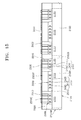
FIG. 13 illustrates a representation of an example of a step of forming a dielectric layer 2500T.
Referring to FIG. 13, the dielectric layer 2500T may be formed on the semiconductor wafer 2100W to cover the second semiconductor chips 2200T and the interposers 2300. The dielectric layer 2500T may be formed to fill gaps between the second semiconductor chips 2200T and the interposers 2300. The dielectric layer 2500T may be formed of an EMC material using a molding process.
FIG. 14 illustrates a representation of an example of a step of reducing the thickness of the second semiconductor chips 2200T and the interposers 2300.
Referring to FIG. 14, the thickness of the second semiconductor chips 2200T and the interposers 2300 may be reduced to expose the ends 2310E of the second internal interconnectors 2310. Specifically, the dielectric layer 2500T may be etched using a planarization process such as a recess process, a polishing process or an etch-back process to expose the second semiconductor chips 2200T and the interposers 2300, and the exposed second semiconductor chips 2200T and the exposed interposers 2300 may also be etched using the planarization process until the ends 2310E of the second internal interconnectors 2310 are exposed. As a result, the second semiconductor chips 2200T and the interposers 2300 may be planarized to have a thickness less than the initial thicknesses T1 and T2. Even though the initial thickness T1 of the second semiconductor chips 2200T is different from the initial thickness T2 of the interposers 2300, the thickness of the planarized second semiconductor chips 2200T may be substantially equal to the thickness of the planarised interposers 2300. Thus, surfaces of the planarized second semiconductor chips 2200T opposite to the semiconductor wafer 2100W may be substantially coplanar with surfaces of the planarised interposers 2300 opposite to the semiconductor wafer 2100W.
FIG. 15 illustrates a representation of an example of a step of forming external interconnectors 2600.
Referring to FIG. 15, the external interconnectors 2600 may be formed on the surfaces of the planarized second semiconductor chips 2200T, the planarised interposers 2300 and the planarized dielectric layer 2500. The external interconnectors 2600 may be used as redistribution lines. The external interconnectors 2600 may be formed by depositing a conductive layer and by patterning the conductive layer. The external interconnectors 2600 may be formed to have trace pattern shapes. The surfaces of the planarized second semiconductor chips 2200T, the planarised interposers 2300 and the planarized dielectric layer 2500 may provide a global flat surface without uneven surface profiles. Accordingly, the external interconnectors 2600 may be formed to have a fine size. That is, the external interconnectors 2600 may be formed to have a fine pitch and may be used as highly integrated circuit patterns.
FIG. 16 illustrates a representation of an example of a step of forming first external connectors 2700.
Referring to FIG. 16, a second protection layer 2650 may be formed on the surfaces of the planarized second semiconductor chips 2200T, the planarised interposers 2300 and the planarized dielectric layer 2500. The second protection layer 2650 may be formed to expose external contact portions of the external interconnectors 2600. The second protection layer 2650 may be formed to include a solder resist layer. The first external connectors 2700 may be formed on the exposed contact portions of the external interconnectors 2600.
FIG. 17 illustrates a representation of an example of a step of forming separate semiconductor packages.
Referring to FIG. 17, the wafer 2100W may be separated into a plurality of semiconductor packages using a die sawing process performed along the scribe lanes 2100S. Each of the semiconductor packages may correspond to any of the semiconductor packages 10 and 30 described with reference to FIGS. 1 and 3.
As described with reference to FIGS. 10 to 17, the semiconductor packages may be fabricated using a wafer level package technique to provide SIPs.
FIG. 18 is a block diagram illustrating a representation of an example of an electronic system 8710 including at least one of the packages according to some embodiments. The electronic system 8710 may include a controller 8711, an input/output device 8712, and a memory 8713. The package according to an embodiment may be realized to include the controller 8711 and the memory 8713. The controller 8711, the input/output device 8712 and the memory 8713 may be coupled with one another through a bus 8715 providing a path through which data move.
In an embodiment, the controller 8711 may include one or more microprocessor, digital signal processor, microcontroller, and/or logic device capable of performing the same functions as these components. The controller 8711 or the memory 8713 may include one or more of the semiconductor packages according to embodiments of the present disclosure. The input/output device 8712 may include at least one selected among a keypad, a keyboard, a display device, a touchscreen and so forth. The memory 8713 is a device for storing data. The memory 8713 may store data and/or commands to be executed by the controller 8711, and the like.
The memory 8713 may include a volatile memory device such as a DRAM and/or a nonvolatile memory device such as a flash memory. For example, a flash memory may be mounted to an information processing system such as a mobile terminal or a desktop computer. The flash memory may constitute a solid state disk (SSD). In this example, the electronic system 8710 may stably store a large amount of data in a flash memory system.
The electronic system 8710 may further include an interface 8714 configured to transmit and receive data to and from a communication network. The interface 8714 may be a wired or wireless type. For example, the interface 8714 may include an antenna or a wired or wireless transceiver.
The electronic system 8710 may be realized as a mobile system, a personal computer, an industrial computer or a logic system performing various functions. For example, the mobile system may be any one of a personal digital assistant (PDA), a portable computer, a tablet computer, a mobile phone, a smart phone, a wireless phone, a laptop computer, a memory card, a digital music system and an information transmission/reception system.
If the electronic system 8710 is an equipment capable of performing wireless communication, the electronic system 8710 may be used in a communication system such as of CDMA (code division multiple access), GSM (global system for mobile communications), NADC (north American digital cellular), E-TDMA (enhanced-time division multiple access), WCDAM (wideband code division multiple access), CDMA2000, LTE (long term evolution) and Wibro (wireless broadband Internet).
Embodiments of the present disclosure have been disclosed for illustrative purposes. Those skilled in the art will appreciate that various modifications, additions and substitutions are possible, without departing from the scope and spirit of the present disclosure and the accompanying claims.

Claims (19)

What is claimed is:
1. A semiconductor package comprising:
a first semiconductor chip;
a second semiconductor chip disposed to overlap with a portion of the first semiconductor chip and connected to the first semiconductor chip through first coupling structures;
an interposer disposed to overlap with another portion of the first semiconductor chip and connected to the first semiconductor chip through second coupling structures, wherein a first surface of the interposer faces the first semiconductor chip and the interposer includes internal interconnectors extending from the second coupling structures on the first surface to a second surface of the interposer opposite to the first surface; and
external interconnectors disposed on the second surface of the interposer and connected to the internal interconnectors
wherein at least one of the external interconnectors extends onto a first surface of the second semiconductor chip opposite to a second surface of the second semiconductor chip facing the first semiconductor chip.
2. The semiconductor package of claim 1, wherein the interposer and the second semiconductor chip are disposed side-by-side on the first semiconductor chip.
3. The semiconductor package of claim 2, further comprising a dielectric layer configured to fill a gap between the interposer and the second semiconductor chip and expose the second surface of the interposer and the first surface of the second semiconductor chip.
4. The semiconductor package of claim 3, wherein at least one of the external interconnectors extends onto a surface of the dielectric layer adjacent to the second surface of the interposer.
5. The semiconductor package of claim 3, wherein the second surface of the interposer is substantially coplanar with the first surface of the second semiconductor chip.
6. The semiconductor package of claim 3,
wherein a surface of the dielectric layer is substantially coplanar with the second surface of the interposer and the first surface of the second semiconductor chip; and
wherein the surface of the dielectric layer connects the second surface of the interposer to the first surface of the second semiconductor chip.
7. The semiconductor package of claim 1, wherein some of the second coupling structures and some of the internal interconnectors provide first electrical paths electrically connecting the first semiconductor chip to some of the external interconnectors.
8. The semiconductor package of claim 7, wherein the others of the second coupling structures, the others of the internal interconnectors and some of the first coupling structures provide second electrical paths electrically connecting the second semiconductor chip to some of the external interconnectors through the first semiconductor chip.
9. The semiconductor package of claim 8, further comprising first internal interconnectors electrically connecting others of the second coupling structures to some of the first coupling structures.
10. The semiconductor package of claim 8, wherein each of the internal interconnectors includes a through silicon via (TSV) that substantially penetrates the interposer.
11. The semiconductor package of claim 8, wherein the others of the first coupling structures provide third electrical paths electrically connecting the second semiconductor chip to the first semiconductor chip.
12. The semiconductor package of claim 1,
wherein the second semiconductor chip overlaps with a central portion of the first semiconductor chip; and
wherein the interposer includes a first interposer and a second interposer, the first and second interposers overlapping with both edges of the first semiconductor chip, respectively.
13. The semiconductor package of claim 1, further comprising a heat spreader disposed on a first surface of the first semiconductor chip opposite to a second surface of the first semiconductor chip facing the second semiconductor chip,
wherein the second surface of the first semiconductor chip faces the second semiconductor chip and the interposer.
14. The semiconductor package of claim 1, further comprising first external connectors attached to the external interconnectors, respectively.
15. The semiconductor package of claim 14, further comprising:
a package substrate having second external connectors configured for electrically connecting to the first external connectors; and
a protection layer configured to cover the first and second semiconductor chips mounted on the package substrate.
16. The semiconductor package of claim 1, wherein the second semiconductor chip includes a high bandwidth memory (HBM) chip in which a plurality of memory chips having through silicon vias (TSVs) are stacked.
17. The semiconductor package of claim 1,
wherein the first coupling structures includes:
a first group of first connectors disposed on a surface of the first semiconductor chip; and
second connectors disposed on a surface of the second semiconductor chip and respectively combined with the first group of first connectors, and
wherein the second coupling structures includes:
a second group of first connectors disposed on a surface of the first semiconductor chip; and
third connectors disposed on a surface of the interposer and respectively combined with the second group of first connectors.
18. A semiconductor package comprising:
a first semiconductor chip including a first group of first connectors, a second group of first connectors, a third group of first connectors, and a fourth group of first connectors disposed on a surface of the first semiconductor chip and including first internal interconnectors configured for connecting the first group of first connectors to the second group of first connectors;
a second semiconductor chip overlapping with a portion of the first semiconductor chip and including a first group of second connectors and a second group of second connectors disposed on a surface of the second semiconductor chip, wherein the first group of second connectors are respectively combined with the second group of first connectors and the second group of second connectors are respectively combined with the third group of first connectors;
an interposer overlapping with another portion of the first semiconductor chip and including a first group of third connectors respectively combined with the first group of first connectors and a second group of third connectors respectively combined with the fourth group of first connectors, wherein the first group of third connectors and the second group of third connectors are disposed on a first surface of the interposer and the interposer includes internal interconnectors extending from the third connectors to a second surface of the interposer opposite to the first surface; and
external interconnectors disposed on the second surface of the interposer and connected to the internal interconnectors.
19. A semiconductor package comprising:
a first semiconductor chip;
a second semiconductor chip disposed to be electrically connected to a portion of the first semiconductor chip;
an interposer including internal interconnectors electrically connected to another portion of the first semiconductor chip;
a dielectric layer configured to fill a gap between the second semiconductor chip and the interposer and to expose a surface of the second semiconductor chip opposite to the first semiconductor chip and a surface of the interposer opposite to the first semiconductor chip; and
external interconnectors disposed on the surfaces of the second semiconductor chip and the interposer opposite to the first semiconductor chip and on a surface of the dielectric layer,
wherein the external interconnectors are connected to the internal interconnectors.
US14/850,283 2015-04-13 2015-09-10 Semiconductor packages with interposers and methods of manufacturing the same Active US9508688B2 (en)

Applications Claiming Priority (2)

Application Number Priority Date Filing Date Title
KR10-2015-0052037 2015-04-13
KR1020150052037A KR20160122022A (en) 2015-04-13 2015-04-13 Semiconductor package with interposer and method of manufacturing the same

Publications (2)

Publication Number Publication Date
US20160300815A1 US20160300815A1 (en) 2016-10-13
US9508688B2 true US9508688B2 (en) 2016-11-29

Family

ID=57111401

Family Applications (1)

Application Number Title Priority Date Filing Date
US14/850,283 Active US9508688B2 (en) 2015-04-13 2015-09-10 Semiconductor packages with interposers and methods of manufacturing the same

Country Status (4)

Country Link
US (1) US9508688B2 (en)
KR (1) KR20160122022A (en)
CN (1) CN106057788A (en)
TW (1) TWI672787B (en)

Cited By (4)

* Cited by examiner, † Cited by third party
Publication number Priority date Publication date Assignee Title
US10446479B2 (en) * 2012-03-23 2019-10-15 STATS ChipPAC Pte. Ltd. Semiconductor device and method of forming a PoP device with embedded vertical interconnect units
US10707150B2 (en) 2012-03-23 2020-07-07 STATS ChipPAC Pte. Ltd. Semiconductor device and method of forming a fan-out PoP device with PWB vertical interconnect units
US11183474B2 (en) * 2019-11-04 2021-11-23 Advanced Semiconductor Engineering, Inc. Electronic device package and method for manufacturing the same
US11251155B2 (en) 2019-05-30 2022-02-15 Samsung Electronics Co., Ltd. Semiconductor package

Families Citing this family (20)

* Cited by examiner, † Cited by third party
Publication number Priority date Publication date Assignee Title
US9859896B1 (en) * 2015-09-11 2018-01-02 Xilinx, Inc. Distributed multi-die routing in a multi-chip module
US9881908B2 (en) * 2016-01-15 2018-01-30 Taiwan Semiconductor Manufacturing Company, Ltd. Integrated fan-out package on package structure and methods of forming same
US10153261B2 (en) * 2017-04-03 2018-12-11 Cisco Technology, Inc. Cooling system for high power application specific integrated circuit with embedded high bandwidth memory
US9899305B1 (en) * 2017-04-28 2018-02-20 Taiwan Semiconductor Manufacturing Company Ltd. Semiconductor package structure
US10283474B2 (en) * 2017-06-30 2019-05-07 Taiwan Semiconductor Manufacturing Co., Ltd. Chip package structure and method for forming the same
WO2019075205A1 (en) * 2017-10-11 2019-04-18 Octavo Systems Llc High performance module for sip
TWI736780B (en) 2017-10-31 2021-08-21 台灣積體電路製造股份有限公司 Chip package and methods of forming the same
US11322449B2 (en) * 2017-10-31 2022-05-03 Taiwan Semiconductor Manufacturing Co., Ltd. Package with fan-out structures
US10515929B2 (en) * 2018-04-09 2019-12-24 International Business Machines Corporation Carrier and integrated memory
US10431563B1 (en) 2018-04-09 2019-10-01 International Business Machines Corporation Carrier and integrated memory
KR102517464B1 (en) * 2018-04-30 2023-04-04 에스케이하이닉스 주식회사 Semiconductor package include bridge die spaced apart semiconductor die
DE102018119538A1 (en) * 2018-08-10 2020-02-13 Osram Opto Semiconductors Gmbh OPTOELECTRONIC SEMICONDUCTOR COMPONENT AND PRODUCTION METHOD FOR OPTOELECTRONIC SEMICONDUCTOR COMPONENTS
KR102609445B1 (en) * 2018-10-22 2023-12-04 삼성전자주식회사 Semiconductor package
KR102530320B1 (en) 2018-11-21 2023-05-09 삼성전자주식회사 Semiconductor package
WO2020147107A1 (en) * 2019-01-18 2020-07-23 华为技术有限公司 Integrated circuit comprising multiple interconnected interposers
KR20200092566A (en) * 2019-01-25 2020-08-04 에스케이하이닉스 주식회사 Semiconductor package including bridge die
US10727215B1 (en) * 2019-01-30 2020-07-28 Sandisk Technologies Llc Three-dimensional memory device with logic signal routing through a memory die and methods of making the same
US11728238B2 (en) * 2019-07-29 2023-08-15 Taiwan Semiconductor Manufacturing Company, Ltd. Semiconductor package with heat dissipation films and manufacturing method thereof
US11600562B2 (en) * 2020-10-21 2023-03-07 Taiwan Semiconductor Manufacturing Company, Ltd. Semiconductor packages and method of manufacturing the same
CN115377017A (en) * 2021-05-17 2022-11-22 中科寒武纪科技股份有限公司 Chip, wafer, equipment with CoWOS packaging structure and generation method thereof

Citations (8)

* Cited by examiner, † Cited by third party
Publication number Priority date Publication date Assignee Title
US20100290193A1 (en) * 2009-05-15 2010-11-18 Industrial Technology Research Institute Stacked-chip packaging structure and fabrication method thereof
KR20130033375A (en) 2010-06-30 2013-04-03 인텔 코오퍼레이션 Bumpless build-up layer package design with an interposer
US20140029639A1 (en) * 2011-12-28 2014-01-30 Edward A. Zarbock Photonic package architecture
US20140191419A1 (en) * 2011-12-22 2014-07-10 Intel Corporation 3d integrated circuit package with window interposer
US20140217604A1 (en) * 2013-02-04 2014-08-07 Taiwan Semiconductor Manufacturing Company, Ltd. Package Structure and Methods of Forming Same
US20140217610A1 (en) * 2010-02-26 2014-08-07 Taiwan Semiconductor Manufacturing Company, Ltd. 3D Semiconductor Package Interposer with Die Cavity
US20160027764A1 (en) * 2014-07-24 2016-01-28 Jong-Kook Kim Semiconductor package stack structure having interposer substrate
US20160064328A1 (en) * 2014-08-26 2016-03-03 Xilinx, Inc. Multi-chip silicon substrate-less chip packaging

Family Cites Families (6)

* Cited by examiner, † Cited by third party
Publication number Priority date Publication date Assignee Title
US5977640A (en) * 1998-06-26 1999-11-02 International Business Machines Corporation Highly integrated chip-on-chip packaging
US20050104211A1 (en) * 2002-05-07 2005-05-19 Shinji Baba Semiconductor device having semiconductor chips mounted on package substrate
US8143097B2 (en) * 2009-09-23 2012-03-27 Stats Chippac, Ltd. Semiconductor device and method of forming open cavity in TSV interposer to contain semiconductor die in WLCSMP
US9099444B2 (en) * 2011-12-22 2015-08-04 Intel Corporation 3D integrated circuit package with through-mold first level interconnects
DE112012006033T5 (en) * 2012-03-13 2015-02-26 Intel Corp. Mounting a microelectronic device on a reverse microelectronic package
US20150014852A1 (en) * 2013-07-12 2015-01-15 Yueli Liu Package assembly configurations for multiple dies and associated techniques

Patent Citations (8)

* Cited by examiner, † Cited by third party
Publication number Priority date Publication date Assignee Title
US20100290193A1 (en) * 2009-05-15 2010-11-18 Industrial Technology Research Institute Stacked-chip packaging structure and fabrication method thereof
US20140217610A1 (en) * 2010-02-26 2014-08-07 Taiwan Semiconductor Manufacturing Company, Ltd. 3D Semiconductor Package Interposer with Die Cavity
KR20130033375A (en) 2010-06-30 2013-04-03 인텔 코오퍼레이션 Bumpless build-up layer package design with an interposer
US20140191419A1 (en) * 2011-12-22 2014-07-10 Intel Corporation 3d integrated circuit package with window interposer
US20140029639A1 (en) * 2011-12-28 2014-01-30 Edward A. Zarbock Photonic package architecture
US20140217604A1 (en) * 2013-02-04 2014-08-07 Taiwan Semiconductor Manufacturing Company, Ltd. Package Structure and Methods of Forming Same
US20160027764A1 (en) * 2014-07-24 2016-01-28 Jong-Kook Kim Semiconductor package stack structure having interposer substrate
US20160064328A1 (en) * 2014-08-26 2016-03-03 Xilinx, Inc. Multi-chip silicon substrate-less chip packaging

Cited By (8)

* Cited by examiner, † Cited by third party
Publication number Priority date Publication date Assignee Title
US10446479B2 (en) * 2012-03-23 2019-10-15 STATS ChipPAC Pte. Ltd. Semiconductor device and method of forming a PoP device with embedded vertical interconnect units
US10707150B2 (en) 2012-03-23 2020-07-07 STATS ChipPAC Pte. Ltd. Semiconductor device and method of forming a fan-out PoP device with PWB vertical interconnect units
US11024561B2 (en) 2012-03-23 2021-06-01 STATS ChipPAC Pte. Ltd. Semiconductor device and method of forming a fan-out PoP device with PWB vertical interconnect units
US11251155B2 (en) 2019-05-30 2022-02-15 Samsung Electronics Co., Ltd. Semiconductor package
US11688719B2 (en) 2019-05-30 2023-06-27 Samsung Electronics Co., Ltd. Semiconductor package
US11955458B2 (en) 2019-05-30 2024-04-09 Samsung Electronics Co., Ltd. Semiconductor package
US11183474B2 (en) * 2019-11-04 2021-11-23 Advanced Semiconductor Engineering, Inc. Electronic device package and method for manufacturing the same
US11837566B2 (en) 2019-11-04 2023-12-05 Advanced Semiconductor Engineering, Inc. Electronic device package and method for manufacturing the same

Also Published As

Publication number Publication date
US20160300815A1 (en) 2016-10-13
TWI672787B (en) 2019-09-21
TW201637166A (en) 2016-10-16
KR20160122022A (en) 2016-10-21
CN106057788A (en) 2016-10-26

Similar Documents

Publication Publication Date Title
US9508688B2 (en) Semiconductor packages with interposers and methods of manufacturing the same
US9748201B2 (en) Semiconductor packages including an interposer
US20170179078A1 (en) Semiconductor packages and methods of manufacturing the same
US10170456B2 (en) Semiconductor packages including heat transferring blocks and methods of manufacturing the same
US9153557B2 (en) Chip stack embedded packages
US9406584B2 (en) Semiconductor package and method for manufacturing the same
US9941253B1 (en) Semiconductor packages including interconnectors and methods of fabricating the same
US10658332B2 (en) Stack packages including bridge dies
US9252141B2 (en) Semiconductor integrated circuit, method for fabricating the same, and semiconductor package
TWI810380B (en) System-in-packages including a bridge die
US9847285B1 (en) Semiconductor packages including heat spreaders and methods of manufacturing the same
US10903131B2 (en) Semiconductor packages including bridge die spaced apart from semiconductor die
US20150054148A1 (en) Semiconductor packages including heat exhaust part
US9711482B2 (en) Semiconductor package embedded with plurality of chips and method of manufacturing the same
US20180286835A1 (en) Semiconductor packages and methods of manufacturing the same
US20150245487A1 (en) Semiconductor package
US9847322B2 (en) Semiconductor packages including through mold ball connectors and methods of manufacturing the same
US9508699B2 (en) Semiconductor package and method for manufacturing the same
US10361141B2 (en) Semiconductor packages relating to thermal transfer plate and methods of manufacturing the same
US20190043833A1 (en) Semiconductor packages including a plurality of stacked dies
US20170287734A1 (en) Semiconductor packages including interposer and methods of manufacturing the same
US20210225771A1 (en) High density pillar interconnect conversion with stack to substrate connection
US11018056B1 (en) Encapsulated solder TSV insertion interconnect

Legal Events

Date Code Title Description
AS Assignment

Owner name: SK HYNIX INC., KOREA, REPUBLIC OF

Free format text: ASSIGNMENT OF ASSIGNORS INTEREST;ASSIGNOR:KIM, JONG HOON;REEL/FRAME:036585/0381

Effective date: 20150806

STCF Information on status: patent grant

Free format text: PATENTED CASE

FEPP Fee payment procedure

Free format text: PAYOR NUMBER ASSIGNED (ORIGINAL EVENT CODE: ASPN); ENTITY STATUS OF PATENT OWNER: LARGE ENTITY

MAFP Maintenance fee payment

Free format text: PAYMENT OF MAINTENANCE FEE, 4TH YEAR, LARGE ENTITY (ORIGINAL EVENT CODE: M1551); ENTITY STATUS OF PATENT OWNER: LARGE ENTITY

Year of fee payment: 4

MAFP Maintenance fee payment

Free format text: PAYMENT OF MAINTENANCE FEE, 8TH YEAR, LARGE ENTITY (ORIGINAL EVENT CODE: M1552); ENTITY STATUS OF PATENT OWNER: LARGE ENTITY

Year of fee payment: 8