US9485496B2 - Systems and methods for measuring depth using images captured by a camera array including cameras surrounding a central camera - Google Patents
Systems and methods for measuring depth using images captured by a camera array including cameras surrounding a central camera Download PDFInfo
- Publication number
- US9485496B2 US9485496B2 US15/095,930 US201615095930A US9485496B2 US 9485496 B2 US9485496 B2 US 9485496B2 US 201615095930 A US201615095930 A US 201615095930A US 9485496 B2 US9485496 B2 US 9485496B2
- Authority
- US
- United States
- Prior art keywords
- camera
- cameras
- imagers
- array
- images
- Prior art date
- Legal status (The legal status is an assumption and is not a legal conclusion. Google has not performed a legal analysis and makes no representation as to the accuracy of the status listed.)
- Active
Links
- 238000000034 method Methods 0.000 title abstract description 41
- 238000003384 imaging method Methods 0.000 claims abstract description 39
- 239000000758 substrate Substances 0.000 claims abstract description 21
- 238000012545 processing Methods 0.000 claims description 44
- 230000003595 spectral effect Effects 0.000 claims description 32
- 238000005259 measurement Methods 0.000 claims description 16
- 238000012790 confirmation Methods 0.000 claims description 11
- 238000009826 distribution Methods 0.000 claims description 4
- 239000004065 semiconductor Substances 0.000 claims description 4
- 230000001788 irregular Effects 0.000 claims description 2
- 230000003287 optical effect Effects 0.000 abstract description 29
- 238000005516 engineering process Methods 0.000 abstract description 5
- 241000023320 Luma <angiosperm> Species 0.000 description 30
- OSWPMRLSEDHDFF-UHFFFAOYSA-N methyl salicylate Chemical compound COC(=O)C1=CC=CC=C1O OSWPMRLSEDHDFF-UHFFFAOYSA-N 0.000 description 30
- 230000008569 process Effects 0.000 description 27
- 238000003491 array Methods 0.000 description 23
- 238000005070 sampling Methods 0.000 description 23
- 235000012431 wafers Nutrition 0.000 description 21
- 230000001965 increasing effect Effects 0.000 description 17
- 230000006870 function Effects 0.000 description 12
- 238000001228 spectrum Methods 0.000 description 11
- 238000006243 chemical reaction Methods 0.000 description 8
- 230000008901 benefit Effects 0.000 description 7
- 238000013461 design Methods 0.000 description 7
- 238000010586 diagram Methods 0.000 description 7
- 239000000463 material Substances 0.000 description 7
- 238000000926 separation method Methods 0.000 description 7
- 238000002329 infrared spectrum Methods 0.000 description 6
- 238000013507 mapping Methods 0.000 description 6
- 230000035945 sensitivity Effects 0.000 description 6
- 238000001429 visible spectrum Methods 0.000 description 6
- 230000004075 alteration Effects 0.000 description 5
- 238000004364 calculation method Methods 0.000 description 5
- 230000008859 change Effects 0.000 description 5
- 238000012937 correction Methods 0.000 description 5
- 230000004927 fusion Effects 0.000 description 5
- 230000010354 integration Effects 0.000 description 5
- 238000004519 manufacturing process Methods 0.000 description 5
- 230000009467 reduction Effects 0.000 description 5
- 101100385324 Arabidopsis thaliana CRA1 gene Proteins 0.000 description 4
- 206010034960 Photophobia Diseases 0.000 description 4
- 238000004422 calculation algorithm Methods 0.000 description 4
- 230000000875 corresponding effect Effects 0.000 description 4
- 230000000694 effects Effects 0.000 description 4
- 208000013469 light sensitivity Diseases 0.000 description 4
- 230000004044 response Effects 0.000 description 4
- 125000006850 spacer group Chemical group 0.000 description 4
- 238000003860 storage Methods 0.000 description 4
- 238000012546 transfer Methods 0.000 description 4
- 238000011144 upstream manufacturing Methods 0.000 description 4
- 230000004931 aggregating effect Effects 0.000 description 3
- 238000013459 approach Methods 0.000 description 3
- 230000000903 blocking effect Effects 0.000 description 3
- 238000000701 chemical imaging Methods 0.000 description 3
- 238000003745 diagnosis Methods 0.000 description 3
- 238000011084 recovery Methods 0.000 description 3
- 229910052710 silicon Inorganic materials 0.000 description 3
- 239000010703 silicon Substances 0.000 description 3
- 230000001360 synchronised effect Effects 0.000 description 3
- VYZAMTAEIAYCRO-UHFFFAOYSA-N Chromium Chemical compound [Cr] VYZAMTAEIAYCRO-UHFFFAOYSA-N 0.000 description 2
- XUIMIQQOPSSXEZ-UHFFFAOYSA-N Silicon Chemical compound [Si] XUIMIQQOPSSXEZ-UHFFFAOYSA-N 0.000 description 2
- 230000015572 biosynthetic process Effects 0.000 description 2
- 229910052804 chromium Inorganic materials 0.000 description 2
- 239000011651 chromium Substances 0.000 description 2
- 239000003086 colorant Substances 0.000 description 2
- 238000004590 computer program Methods 0.000 description 2
- 230000001276 controlling effect Effects 0.000 description 2
- 230000003247 decreasing effect Effects 0.000 description 2
- 230000007547 defect Effects 0.000 description 2
- 238000001514 detection method Methods 0.000 description 2
- 238000005538 encapsulation Methods 0.000 description 2
- 238000005530 etching Methods 0.000 description 2
- 239000011521 glass Substances 0.000 description 2
- 238000005286 illumination Methods 0.000 description 2
- 230000006872 improvement Effects 0.000 description 2
- 238000012804 iterative process Methods 0.000 description 2
- 239000011159 matrix material Substances 0.000 description 2
- 230000015654 memory Effects 0.000 description 2
- 238000000465 moulding Methods 0.000 description 2
- 238000010606 normalization Methods 0.000 description 2
- 229920006395 saturated elastomer Polymers 0.000 description 2
- 230000007704 transition Effects 0.000 description 2
- 208000010201 Exanthema Diseases 0.000 description 1
- 241000593989 Scardinius erythrophthalmus Species 0.000 description 1
- ATJFFYVFTNAWJD-UHFFFAOYSA-N Tin Chemical compound [Sn] ATJFFYVFTNAWJD-UHFFFAOYSA-N 0.000 description 1
- 206010052428 Wound Diseases 0.000 description 1
- 208000027418 Wounds and injury Diseases 0.000 description 1
- 230000005856 abnormality Effects 0.000 description 1
- 230000003213 activating effect Effects 0.000 description 1
- 230000003044 adaptive effect Effects 0.000 description 1
- 230000002776 aggregation Effects 0.000 description 1
- 238000004220 aggregation Methods 0.000 description 1
- 238000004458 analytical method Methods 0.000 description 1
- 230000002146 bilateral effect Effects 0.000 description 1
- 238000012512 characterization method Methods 0.000 description 1
- 238000004891 communication Methods 0.000 description 1
- 230000000295 complement effect Effects 0.000 description 1
- 230000006835 compression Effects 0.000 description 1
- 238000007906 compression Methods 0.000 description 1
- 238000010276 construction Methods 0.000 description 1
- 230000002596 correlated effect Effects 0.000 description 1
- 230000001934 delay Effects 0.000 description 1
- 230000001419 dependent effect Effects 0.000 description 1
- 238000002059 diagnostic imaging Methods 0.000 description 1
- 230000009977 dual effect Effects 0.000 description 1
- 201000005884 exanthem Diseases 0.000 description 1
- 238000009499 grossing Methods 0.000 description 1
- 238000003709 image segmentation Methods 0.000 description 1
- 230000001939 inductive effect Effects 0.000 description 1
- 230000007246 mechanism Effects 0.000 description 1
- 239000000203 mixture Substances 0.000 description 1
- 238000012986 modification Methods 0.000 description 1
- 230000004048 modification Effects 0.000 description 1
- 201000005111 ocular hyperemia Diseases 0.000 description 1
- 238000004806 packaging method and process Methods 0.000 description 1
- 238000012858 packaging process Methods 0.000 description 1
- 238000010422 painting Methods 0.000 description 1
- 230000000704 physical effect Effects 0.000 description 1
- 238000007747 plating Methods 0.000 description 1
- 206010037844 rash Diseases 0.000 description 1
- 238000002310 reflectometry Methods 0.000 description 1
- 238000009877 rendering Methods 0.000 description 1
- 238000013341 scale-up Methods 0.000 description 1
- 230000011218 segmentation Effects 0.000 description 1
- 238000004088 simulation Methods 0.000 description 1
- 229910000679 solder Inorganic materials 0.000 description 1
- 239000000126 substance Substances 0.000 description 1
- 208000024891 symptom Diseases 0.000 description 1
Images


Classifications
-
- H—ELECTRICITY
- H04—ELECTRIC COMMUNICATION TECHNIQUE
- H04N—PICTORIAL COMMUNICATION, e.g. TELEVISION
- H04N23/00—Cameras or camera modules comprising electronic image sensors; Control thereof
- H04N23/90—Arrangement of cameras or camera modules, e.g. multiple cameras in TV studios or sports stadiums
-
- H—ELECTRICITY
- H04—ELECTRIC COMMUNICATION TECHNIQUE
- H04N—PICTORIAL COMMUNICATION, e.g. TELEVISION
- H04N23/00—Cameras or camera modules comprising electronic image sensors; Control thereof
- H04N23/80—Camera processing pipelines; Components thereof
-
- H—ELECTRICITY
- H01—ELECTRIC ELEMENTS
- H01L—SEMICONDUCTOR DEVICES NOT COVERED BY CLASS H10
- H01L27/00—Devices consisting of a plurality of semiconductor or other solid-state components formed in or on a common substrate
- H01L27/14—Devices consisting of a plurality of semiconductor or other solid-state components formed in or on a common substrate including semiconductor components sensitive to infrared radiation, light, electromagnetic radiation of shorter wavelength or corpuscular radiation and specially adapted either for the conversion of the energy of such radiation into electrical energy or for the control of electrical energy by such radiation
- H01L27/144—Devices controlled by radiation
- H01L27/146—Imager structures
- H01L27/14601—Structural or functional details thereof
- H01L27/14618—Containers
-
- H04N13/0242—
-
- G—PHYSICS
- G02—OPTICS
- G02B—OPTICAL ELEMENTS, SYSTEMS OR APPARATUS
- G02B13/00—Optical objectives specially designed for the purposes specified below
- G02B13/001—Miniaturised objectives for electronic devices, e.g. portable telephones, webcams, PDAs, small digital cameras
- G02B13/0015—Miniaturised objectives for electronic devices, e.g. portable telephones, webcams, PDAs, small digital cameras characterised by the lens design
-
- G—PHYSICS
- G02—OPTICS
- G02B—OPTICAL ELEMENTS, SYSTEMS OR APPARATUS
- G02B13/00—Optical objectives specially designed for the purposes specified below
- G02B13/001—Miniaturised objectives for electronic devices, e.g. portable telephones, webcams, PDAs, small digital cameras
- G02B13/0085—Miniaturised objectives for electronic devices, e.g. portable telephones, webcams, PDAs, small digital cameras employing wafer level optics
-
- G—PHYSICS
- G02—OPTICS
- G02B—OPTICAL ELEMENTS, SYSTEMS OR APPARATUS
- G02B27/00—Optical systems or apparatus not provided for by any of the groups G02B1/00 - G02B26/00, G02B30/00
- G02B27/0025—Optical systems or apparatus not provided for by any of the groups G02B1/00 - G02B26/00, G02B30/00 for optical correction, e.g. distorsion, aberration
-
- G—PHYSICS
- G02—OPTICS
- G02B—OPTICAL ELEMENTS, SYSTEMS OR APPARATUS
- G02B27/00—Optical systems or apparatus not provided for by any of the groups G02B1/00 - G02B26/00, G02B30/00
- G02B27/10—Beam splitting or combining systems
- G02B27/1066—Beam splitting or combining systems for enhancing image performance, like resolution, pixel numbers, dual magnifications or dynamic range, by tiling, slicing or overlapping fields of view
-
- G—PHYSICS
- G02—OPTICS
- G02B—OPTICAL ELEMENTS, SYSTEMS OR APPARATUS
- G02B27/00—Optical systems or apparatus not provided for by any of the groups G02B1/00 - G02B26/00, G02B30/00
- G02B27/10—Beam splitting or combining systems
- G02B27/12—Beam splitting or combining systems operating by refraction only
- G02B27/123—The splitting element being a lens or a system of lenses, including arrays and surfaces with refractive power
-
- G—PHYSICS
- G02—OPTICS
- G02B—OPTICAL ELEMENTS, SYSTEMS OR APPARATUS
- G02B3/00—Simple or compound lenses
- G02B3/0006—Arrays
-
- G—PHYSICS
- G02—OPTICS
- G02B—OPTICAL ELEMENTS, SYSTEMS OR APPARATUS
- G02B5/00—Optical elements other than lenses
- G02B5/20—Filters
-
- G—PHYSICS
- G02—OPTICS
- G02B—OPTICAL ELEMENTS, SYSTEMS OR APPARATUS
- G02B5/00—Optical elements other than lenses
- G02B5/20—Filters
- G02B5/208—Filters for use with infrared or ultraviolet radiation, e.g. for separating visible light from infrared and/or ultraviolet radiation
-
- G—PHYSICS
- G06—COMPUTING; CALCULATING OR COUNTING
- G06T—IMAGE DATA PROCESSING OR GENERATION, IN GENERAL
- G06T1/00—General purpose image data processing
- G06T1/20—Processor architectures; Processor configuration, e.g. pipelining
-
- G—PHYSICS
- G06—COMPUTING; CALCULATING OR COUNTING
- G06T—IMAGE DATA PROCESSING OR GENERATION, IN GENERAL
- G06T3/00—Geometric image transformation in the plane of the image
- G06T3/40—Scaling the whole image or part thereof
- G06T3/4053—Super resolution, i.e. output image resolution higher than sensor resolution
-
- G—PHYSICS
- G06—COMPUTING; CALCULATING OR COUNTING
- G06T—IMAGE DATA PROCESSING OR GENERATION, IN GENERAL
- G06T7/00—Image analysis
- G06T7/50—Depth or shape recovery
-
- G—PHYSICS
- G06—COMPUTING; CALCULATING OR COUNTING
- G06T—IMAGE DATA PROCESSING OR GENERATION, IN GENERAL
- G06T7/00—Image analysis
- G06T7/50—Depth or shape recovery
- G06T7/55—Depth or shape recovery from multiple images
-
- G—PHYSICS
- G06—COMPUTING; CALCULATING OR COUNTING
- G06T—IMAGE DATA PROCESSING OR GENERATION, IN GENERAL
- G06T7/00—Image analysis
- G06T7/50—Depth or shape recovery
- G06T7/55—Depth or shape recovery from multiple images
- G06T7/557—Depth or shape recovery from multiple images from light fields, e.g. from plenoptic cameras
-
- G—PHYSICS
- G06—COMPUTING; CALCULATING OR COUNTING
- G06T—IMAGE DATA PROCESSING OR GENERATION, IN GENERAL
- G06T7/00—Image analysis
- G06T7/70—Determining position or orientation of objects or cameras
-
- H—ELECTRICITY
- H01—ELECTRIC ELEMENTS
- H01L—SEMICONDUCTOR DEVICES NOT COVERED BY CLASS H10
- H01L27/00—Devices consisting of a plurality of semiconductor or other solid-state components formed in or on a common substrate
- H01L27/14—Devices consisting of a plurality of semiconductor or other solid-state components formed in or on a common substrate including semiconductor components sensitive to infrared radiation, light, electromagnetic radiation of shorter wavelength or corpuscular radiation and specially adapted either for the conversion of the energy of such radiation into electrical energy or for the control of electrical energy by such radiation
- H01L27/144—Devices controlled by radiation
- H01L27/146—Imager structures
- H01L27/14601—Structural or functional details thereof
- H01L27/1462—Coatings
- H01L27/14621—Colour filter arrangements
-
- H—ELECTRICITY
- H01—ELECTRIC ELEMENTS
- H01L—SEMICONDUCTOR DEVICES NOT COVERED BY CLASS H10
- H01L27/00—Devices consisting of a plurality of semiconductor or other solid-state components formed in or on a common substrate
- H01L27/14—Devices consisting of a plurality of semiconductor or other solid-state components formed in or on a common substrate including semiconductor components sensitive to infrared radiation, light, electromagnetic radiation of shorter wavelength or corpuscular radiation and specially adapted either for the conversion of the energy of such radiation into electrical energy or for the control of electrical energy by such radiation
- H01L27/144—Devices controlled by radiation
- H01L27/146—Imager structures
- H01L27/14601—Structural or functional details thereof
- H01L27/14625—Optical elements or arrangements associated with the device
-
- H—ELECTRICITY
- H01—ELECTRIC ELEMENTS
- H01L—SEMICONDUCTOR DEVICES NOT COVERED BY CLASS H10
- H01L27/00—Devices consisting of a plurality of semiconductor or other solid-state components formed in or on a common substrate
- H01L27/14—Devices consisting of a plurality of semiconductor or other solid-state components formed in or on a common substrate including semiconductor components sensitive to infrared radiation, light, electromagnetic radiation of shorter wavelength or corpuscular radiation and specially adapted either for the conversion of the energy of such radiation into electrical energy or for the control of electrical energy by such radiation
- H01L27/144—Devices controlled by radiation
- H01L27/146—Imager structures
- H01L27/14601—Structural or functional details thereof
- H01L27/14632—Wafer-level processed structures
-
- H—ELECTRICITY
- H01—ELECTRIC ELEMENTS
- H01L—SEMICONDUCTOR DEVICES NOT COVERED BY CLASS H10
- H01L27/00—Devices consisting of a plurality of semiconductor or other solid-state components formed in or on a common substrate
- H01L27/14—Devices consisting of a plurality of semiconductor or other solid-state components formed in or on a common substrate including semiconductor components sensitive to infrared radiation, light, electromagnetic radiation of shorter wavelength or corpuscular radiation and specially adapted either for the conversion of the energy of such radiation into electrical energy or for the control of electrical energy by such radiation
- H01L27/144—Devices controlled by radiation
- H01L27/146—Imager structures
- H01L27/14683—Processes or apparatus peculiar to the manufacture or treatment of these devices or parts thereof
- H01L27/14685—Process for coatings or optical elements
-
- H—ELECTRICITY
- H01—ELECTRIC ELEMENTS
- H01L—SEMICONDUCTOR DEVICES NOT COVERED BY CLASS H10
- H01L27/00—Devices consisting of a plurality of semiconductor or other solid-state components formed in or on a common substrate
- H01L27/14—Devices consisting of a plurality of semiconductor or other solid-state components formed in or on a common substrate including semiconductor components sensitive to infrared radiation, light, electromagnetic radiation of shorter wavelength or corpuscular radiation and specially adapted either for the conversion of the energy of such radiation into electrical energy or for the control of electrical energy by such radiation
- H01L27/144—Devices controlled by radiation
- H01L27/146—Imager structures
- H01L27/14683—Processes or apparatus peculiar to the manufacture or treatment of these devices or parts thereof
- H01L27/14687—Wafer level processing
-
- H—ELECTRICITY
- H04—ELECTRIC COMMUNICATION TECHNIQUE
- H04N—PICTORIAL COMMUNICATION, e.g. TELEVISION
- H04N1/00—Scanning, transmission or reproduction of documents or the like, e.g. facsimile transmission; Details thereof
- H04N1/04—Scanning arrangements, i.e. arrangements for the displacement of active reading or reproducing elements relative to the original or reproducing medium, or vice versa
- H04N1/19—Scanning arrangements, i.e. arrangements for the displacement of active reading or reproducing elements relative to the original or reproducing medium, or vice versa using multi-element arrays
- H04N1/195—Scanning arrangements, i.e. arrangements for the displacement of active reading or reproducing elements relative to the original or reproducing medium, or vice versa using multi-element arrays the array comprising a two-dimensional array or a combination of two-dimensional arrays
- H04N1/19589—Optical means, e.g. an optical fibre bundle, for mapping the whole or a part of a scanned image onto the array
-
- H—ELECTRICITY
- H04—ELECTRIC COMMUNICATION TECHNIQUE
- H04N—PICTORIAL COMMUNICATION, e.g. TELEVISION
- H04N1/00—Scanning, transmission or reproduction of documents or the like, e.g. facsimile transmission; Details thereof
- H04N1/04—Scanning arrangements, i.e. arrangements for the displacement of active reading or reproducing elements relative to the original or reproducing medium, or vice versa
- H04N1/19—Scanning arrangements, i.e. arrangements for the displacement of active reading or reproducing elements relative to the original or reproducing medium, or vice versa using multi-element arrays
- H04N1/195—Scanning arrangements, i.e. arrangements for the displacement of active reading or reproducing elements relative to the original or reproducing medium, or vice versa using multi-element arrays the array comprising a two-dimensional array or a combination of two-dimensional arrays
- H04N1/19594—Scanning arrangements, i.e. arrangements for the displacement of active reading or reproducing elements relative to the original or reproducing medium, or vice versa using multi-element arrays the array comprising a two-dimensional array or a combination of two-dimensional arrays using a television camera or a still video camera
-
- H04N13/0022—
-
- H04N13/0257—
-
- H—ELECTRICITY
- H04—ELECTRIC COMMUNICATION TECHNIQUE
- H04N—PICTORIAL COMMUNICATION, e.g. TELEVISION
- H04N13/00—Stereoscopic video systems; Multi-view video systems; Details thereof
- H04N13/10—Processing, recording or transmission of stereoscopic or multi-view image signals
- H04N13/106—Processing image signals
- H04N13/128—Adjusting depth or disparity
-
- H—ELECTRICITY
- H04—ELECTRIC COMMUNICATION TECHNIQUE
- H04N—PICTORIAL COMMUNICATION, e.g. TELEVISION
- H04N13/00—Stereoscopic video systems; Multi-view video systems; Details thereof
- H04N13/20—Image signal generators
- H04N13/204—Image signal generators using stereoscopic image cameras
- H04N13/243—Image signal generators using stereoscopic image cameras using three or more 2D image sensors
-
- H—ELECTRICITY
- H04—ELECTRIC COMMUNICATION TECHNIQUE
- H04N—PICTORIAL COMMUNICATION, e.g. TELEVISION
- H04N13/00—Stereoscopic video systems; Multi-view video systems; Details thereof
- H04N13/20—Image signal generators
- H04N13/257—Colour aspects
-
- H—ELECTRICITY
- H04—ELECTRIC COMMUNICATION TECHNIQUE
- H04N—PICTORIAL COMMUNICATION, e.g. TELEVISION
- H04N23/00—Cameras or camera modules comprising electronic image sensors; Control thereof
- H04N23/10—Cameras or camera modules comprising electronic image sensors; Control thereof for generating image signals from different wavelengths
-
- H—ELECTRICITY
- H04—ELECTRIC COMMUNICATION TECHNIQUE
- H04N—PICTORIAL COMMUNICATION, e.g. TELEVISION
- H04N23/00—Cameras or camera modules comprising electronic image sensors; Control thereof
- H04N23/40—Circuit details for pick-up tubes
-
- H—ELECTRICITY
- H04—ELECTRIC COMMUNICATION TECHNIQUE
- H04N—PICTORIAL COMMUNICATION, e.g. TELEVISION
- H04N23/00—Cameras or camera modules comprising electronic image sensors; Control thereof
- H04N23/45—Cameras or camera modules comprising electronic image sensors; Control thereof for generating image signals from two or more image sensors being of different type or operating in different modes, e.g. with a CMOS sensor for moving images in combination with a charge-coupled device [CCD] for still images
-
- H—ELECTRICITY
- H04—ELECTRIC COMMUNICATION TECHNIQUE
- H04N—PICTORIAL COMMUNICATION, e.g. TELEVISION
- H04N23/00—Cameras or camera modules comprising electronic image sensors; Control thereof
- H04N23/50—Constructional details
- H04N23/54—Mounting of pick-up tubes, electronic image sensors, deviation or focusing coils
-
- H—ELECTRICITY
- H04—ELECTRIC COMMUNICATION TECHNIQUE
- H04N—PICTORIAL COMMUNICATION, e.g. TELEVISION
- H04N23/00—Cameras or camera modules comprising electronic image sensors; Control thereof
- H04N23/50—Constructional details
- H04N23/55—Optical parts specially adapted for electronic image sensors; Mounting thereof
-
- H—ELECTRICITY
- H04—ELECTRIC COMMUNICATION TECHNIQUE
- H04N—PICTORIAL COMMUNICATION, e.g. TELEVISION
- H04N23/00—Cameras or camera modules comprising electronic image sensors; Control thereof
- H04N23/60—Control of cameras or camera modules
-
- H—ELECTRICITY
- H04—ELECTRIC COMMUNICATION TECHNIQUE
- H04N—PICTORIAL COMMUNICATION, e.g. TELEVISION
- H04N23/00—Cameras or camera modules comprising electronic image sensors; Control thereof
- H04N23/60—Control of cameras or camera modules
- H04N23/67—Focus control based on electronic image sensor signals
-
- H—ELECTRICITY
- H04—ELECTRIC COMMUNICATION TECHNIQUE
- H04N—PICTORIAL COMMUNICATION, e.g. TELEVISION
- H04N23/00—Cameras or camera modules comprising electronic image sensors; Control thereof
- H04N23/60—Control of cameras or camera modules
- H04N23/69—Control of means for changing angle of the field of view, e.g. optical zoom objectives or electronic zooming
-
- H—ELECTRICITY
- H04—ELECTRIC COMMUNICATION TECHNIQUE
- H04N—PICTORIAL COMMUNICATION, e.g. TELEVISION
- H04N23/00—Cameras or camera modules comprising electronic image sensors; Control thereof
- H04N23/60—Control of cameras or camera modules
- H04N23/698—Control of cameras or camera modules for achieving an enlarged field of view, e.g. panoramic image capture
-
- H—ELECTRICITY
- H04—ELECTRIC COMMUNICATION TECHNIQUE
- H04N—PICTORIAL COMMUNICATION, e.g. TELEVISION
- H04N23/00—Cameras or camera modules comprising electronic image sensors; Control thereof
- H04N23/95—Computational photography systems, e.g. light-field imaging systems
- H04N23/951—Computational photography systems, e.g. light-field imaging systems by using two or more images to influence resolution, frame rate or aspect ratio
-
- H—ELECTRICITY
- H04—ELECTRIC COMMUNICATION TECHNIQUE
- H04N—PICTORIAL COMMUNICATION, e.g. TELEVISION
- H04N25/00—Circuitry of solid-state image sensors [SSIS]; Control thereof
-
- H—ELECTRICITY
- H04—ELECTRIC COMMUNICATION TECHNIQUE
- H04N—PICTORIAL COMMUNICATION, e.g. TELEVISION
- H04N25/00—Circuitry of solid-state image sensors [SSIS]; Control thereof
- H04N25/10—Circuitry of solid-state image sensors [SSIS]; Control thereof for transforming different wavelengths into image signals
- H04N25/11—Arrangement of colour filter arrays [CFA]; Filter mosaics
- H04N25/13—Arrangement of colour filter arrays [CFA]; Filter mosaics characterised by the spectral characteristics of the filter elements
- H04N25/131—Arrangement of colour filter arrays [CFA]; Filter mosaics characterised by the spectral characteristics of the filter elements including elements passing infrared wavelengths
-
- H—ELECTRICITY
- H04—ELECTRIC COMMUNICATION TECHNIQUE
- H04N—PICTORIAL COMMUNICATION, e.g. TELEVISION
- H04N25/00—Circuitry of solid-state image sensors [SSIS]; Control thereof
- H04N25/10—Circuitry of solid-state image sensors [SSIS]; Control thereof for transforming different wavelengths into image signals
- H04N25/11—Arrangement of colour filter arrays [CFA]; Filter mosaics
- H04N25/13—Arrangement of colour filter arrays [CFA]; Filter mosaics characterised by the spectral characteristics of the filter elements
- H04N25/134—Arrangement of colour filter arrays [CFA]; Filter mosaics characterised by the spectral characteristics of the filter elements based on three different wavelength filter elements
-
- H—ELECTRICITY
- H04—ELECTRIC COMMUNICATION TECHNIQUE
- H04N—PICTORIAL COMMUNICATION, e.g. TELEVISION
- H04N25/00—Circuitry of solid-state image sensors [SSIS]; Control thereof
- H04N25/10—Circuitry of solid-state image sensors [SSIS]; Control thereof for transforming different wavelengths into image signals
- H04N25/11—Arrangement of colour filter arrays [CFA]; Filter mosaics
- H04N25/13—Arrangement of colour filter arrays [CFA]; Filter mosaics characterised by the spectral characteristics of the filter elements
- H04N25/135—Arrangement of colour filter arrays [CFA]; Filter mosaics characterised by the spectral characteristics of the filter elements based on four or more different wavelength filter elements
-
- H—ELECTRICITY
- H04—ELECTRIC COMMUNICATION TECHNIQUE
- H04N—PICTORIAL COMMUNICATION, e.g. TELEVISION
- H04N25/00—Circuitry of solid-state image sensors [SSIS]; Control thereof
- H04N25/40—Extracting pixel data from image sensors by controlling scanning circuits, e.g. by modifying the number of pixels sampled or to be sampled
- H04N25/41—Extracting pixel data from a plurality of image sensors simultaneously picking up an image, e.g. for increasing the field of view by combining the outputs of a plurality of sensors
-
- H—ELECTRICITY
- H04—ELECTRIC COMMUNICATION TECHNIQUE
- H04N—PICTORIAL COMMUNICATION, e.g. TELEVISION
- H04N25/00—Circuitry of solid-state image sensors [SSIS]; Control thereof
- H04N25/50—Control of the SSIS exposure
- H04N25/53—Control of the integration time
- H04N25/533—Control of the integration time by using differing integration times for different sensor regions
- H04N25/534—Control of the integration time by using differing integration times for different sensor regions depending on the spectral component
-
- H—ELECTRICITY
- H04—ELECTRIC COMMUNICATION TECHNIQUE
- H04N—PICTORIAL COMMUNICATION, e.g. TELEVISION
- H04N25/00—Circuitry of solid-state image sensors [SSIS]; Control thereof
- H04N25/50—Control of the SSIS exposure
- H04N25/57—Control of the dynamic range
- H04N25/58—Control of the dynamic range involving two or more exposures
- H04N25/581—Control of the dynamic range involving two or more exposures acquired simultaneously
-
- H—ELECTRICITY
- H04—ELECTRIC COMMUNICATION TECHNIQUE
- H04N—PICTORIAL COMMUNICATION, e.g. TELEVISION
- H04N25/00—Circuitry of solid-state image sensors [SSIS]; Control thereof
- H04N25/60—Noise processing, e.g. detecting, correcting, reducing or removing noise
-
- H—ELECTRICITY
- H04—ELECTRIC COMMUNICATION TECHNIQUE
- H04N—PICTORIAL COMMUNICATION, e.g. TELEVISION
- H04N25/00—Circuitry of solid-state image sensors [SSIS]; Control thereof
- H04N25/60—Noise processing, e.g. detecting, correcting, reducing or removing noise
- H04N25/616—Noise processing, e.g. detecting, correcting, reducing or removing noise involving a correlated sampling function, e.g. correlated double sampling [CDS] or triple sampling
-
- H—ELECTRICITY
- H04—ELECTRIC COMMUNICATION TECHNIQUE
- H04N—PICTORIAL COMMUNICATION, e.g. TELEVISION
- H04N25/00—Circuitry of solid-state image sensors [SSIS]; Control thereof
- H04N25/70—SSIS architectures; Circuits associated therewith
- H04N25/702—SSIS architectures characterised by non-identical, non-equidistant or non-planar pixel layout
-
- H—ELECTRICITY
- H04—ELECTRIC COMMUNICATION TECHNIQUE
- H04N—PICTORIAL COMMUNICATION, e.g. TELEVISION
- H04N25/00—Circuitry of solid-state image sensors [SSIS]; Control thereof
- H04N25/70—SSIS architectures; Circuits associated therewith
- H04N25/71—Charge-coupled device [CCD] sensors; Charge-transfer registers specially adapted for CCD sensors
- H04N25/74—Circuitry for scanning or addressing the pixel array
-
- H—ELECTRICITY
- H04—ELECTRIC COMMUNICATION TECHNIQUE
- H04N—PICTORIAL COMMUNICATION, e.g. TELEVISION
- H04N5/00—Details of television systems
- H04N5/222—Studio circuitry; Studio devices; Studio equipment
- H04N5/262—Studio circuits, e.g. for mixing, switching-over, change of character of image, other special effects ; Cameras specially adapted for the electronic generation of special effects
- H04N5/2621—Cameras specially adapted for the electronic generation of special effects during image pickup, e.g. digital cameras, camcorders, video cameras having integrated special effects capability
-
- H—ELECTRICITY
- H04—ELECTRIC COMMUNICATION TECHNIQUE
- H04N—PICTORIAL COMMUNICATION, e.g. TELEVISION
- H04N5/00—Details of television systems
- H04N5/222—Studio circuitry; Studio devices; Studio equipment
- H04N5/262—Studio circuits, e.g. for mixing, switching-over, change of character of image, other special effects ; Cameras specially adapted for the electronic generation of special effects
- H04N5/265—Mixing
-
- H—ELECTRICITY
- H04—ELECTRIC COMMUNICATION TECHNIQUE
- H04N—PICTORIAL COMMUNICATION, e.g. TELEVISION
- H04N5/00—Details of television systems
- H04N5/30—Transforming light or analogous information into electric information
- H04N5/33—Transforming infrared radiation
-
- G—PHYSICS
- G06—COMPUTING; CALCULATING OR COUNTING
- G06T—IMAGE DATA PROCESSING OR GENERATION, IN GENERAL
- G06T2207/00—Indexing scheme for image analysis or image enhancement
- G06T2207/10—Image acquisition modality
- G06T2207/10052—Images from lightfield camera
-
- G—PHYSICS
- G06—COMPUTING; CALCULATING OR COUNTING
- G06T—IMAGE DATA PROCESSING OR GENERATION, IN GENERAL
- G06T2207/00—Indexing scheme for image analysis or image enhancement
- G06T2207/30—Subject of image; Context of image processing
- G06T2207/30244—Camera pose
-
- H—ELECTRICITY
- H01—ELECTRIC ELEMENTS
- H01L—SEMICONDUCTOR DEVICES NOT COVERED BY CLASS H10
- H01L2924/00—Indexing scheme for arrangements or methods for connecting or disconnecting semiconductor or solid-state bodies as covered by H01L24/00
- H01L2924/0001—Technical content checked by a classifier
- H01L2924/0002—Not covered by any one of groups H01L24/00, H01L24/00 and H01L2224/00
-
- H—ELECTRICITY
- H04—ELECTRIC COMMUNICATION TECHNIQUE
- H04N—PICTORIAL COMMUNICATION, e.g. TELEVISION
- H04N1/00—Scanning, transmission or reproduction of documents or the like, e.g. facsimile transmission; Details thereof
- H04N1/04—Scanning arrangements, i.e. arrangements for the displacement of active reading or reproducing elements relative to the original or reproducing medium, or vice versa
- H04N1/19—Scanning arrangements, i.e. arrangements for the displacement of active reading or reproducing elements relative to the original or reproducing medium, or vice versa using multi-element arrays
- H04N1/195—Scanning arrangements, i.e. arrangements for the displacement of active reading or reproducing elements relative to the original or reproducing medium, or vice versa using multi-element arrays the array comprising a two-dimensional array or a combination of two-dimensional arrays
-
- H—ELECTRICITY
- H04—ELECTRIC COMMUNICATION TECHNIQUE
- H04N—PICTORIAL COMMUNICATION, e.g. TELEVISION
- H04N13/00—Stereoscopic video systems; Multi-view video systems; Details thereof
- H04N2013/0074—Stereoscopic image analysis
- H04N2013/0081—Depth or disparity estimation from stereoscopic image signals
Definitions
- the present invention is related to an image sensor including a plurality of heterogeneous imagers, more specifically to an image sensor with a plurality of wafer-level imagers having custom filters, sensors and optics of varying configurations.
- Image sensors are used in cameras and other imaging devices to capture images.
- light enters through an opening (aperture) at one end of the imaging device and is directed to an image sensor by an optical element such as a lens.
- an optical element such as a lens.
- one or more layers of optical elements are placed between the aperture and the image sensor to focus light onto the image sensor.
- the image sensor consists of pixels that generate signals upon receiving light via the optical element.
- Commonly used image sensors include CCD (charge-coupled device) image sensors and CMOS (complementary metal-oxide-semiconductor) sensors.
- Filters are often employed in the image sensor to selectively transmit lights of certain wavelengths onto pixels.
- a Bayer filter mosaic is often formed on the image sensor.
- the Bayer filter is a color filter array that arranges one of the RGB color filters on each of the color pixels.
- the Bayer filter pattern includes 50% green filters, 25% red filters and 25% blue filters. Since each pixel generates a signal representing strength of a color component in the light and not the full range of colors, demosaicing is performed to interpolate a set of red, green and blue values for each image pixel.
- the image sensors are subject to various performance constraints.
- the performance constraints for the image sensors include, among others, dynamic range, signal to noise (SNR) ratio and low light sensitivity.
- the dynamic range is defined as the ratio of the maximum possible signal that can be captured by a pixel to the total noise signal.
- the well capacity of an image sensor limits the maximum possible signal that can be captured by the image sensor.
- the maximum possible signal in turn is dependent on the strength of the incident illumination and the duration of exposure (e.g., integration time, and shutter width).
- the dynamic range can be expressed as a dimensionless quantity in decibels (dB) as:
- the noise level in the captured image influences the floor of the dynamic range.
- the best case would be 48 dB assuming the RMS noise level is 1 bit. In reality, however, the RMS noise levels are higher than 1 bit, and this further reduces the dynamic range.
- the signal to noise ratio (SNR) of a captured image is, to a great extent, a measure of image quality. In general, as more light is captured by the pixel, the higher the SNR.
- the SNR of a captured image is usually related to the light gathering capability of the pixel.
- Bayer filter sensors have low light sensitivity. At low light levels, each pixel's light gathering capability is constrained by the low signal levels incident upon each pixel. In addition, the color filters over the pixel further constrain the signal reaching the pixel. IR (Infrared) filters also reduce the photo-response from near-IR signals, which can carry valuable information.
- Embodiments provide a camera array, an imaging device including a camera array and/or a method for capturing image that employ a plurality of imagers fabricated on a substrate where each imager includes a plurality of sensor elements.
- the plurality of imagers include at least a first imager formed on a first location of the substrate and a second imager formed on a second location of the substrate.
- the first imager and the second imager may have the same imaging characteristics or different imaging characteristics.
- the first imaging characteristics and the second imager have different imaging characteristics.
- the imaging characteristics may include, among others, the size of the imager, the type of pixels included in the imager, the shape of the imager, filters associated with the imager, exposure time of the imager, aperture size associated with the imager, the configuration of the optical element associated with the imager, gain of the imager, the resolution of the imager, and operational timing of the imager.
- the first imager includes a filter for transmitting a light spectrum.
- the second imager also includes the same type of filter for transmitting the same light spectrum as the first imager but captures an image that is sub-pixel phase shifted from an image captured by the first imager.
- the images from the first imager and the second imager are combined using a super-resolution process to obtain images of higher resolution.
- the first imager includes a first filter for transmitting a first light spectrum and the second imager includes a second filter for transmitting a second light spectrum.
- the images from the first and second imagers are then processed to obtain a higher quality image.
- lens elements are provided to direct and focus light onto the imagers.
- Each lens element focuses light onto one imager. Because each lens element is associated with one imager, each lens element may be designed and configured for a narrow light spectrum. Further, the thickness of the lens element may be reduced, decreasing the overall thickness of the camera array.
- the lens elements are fabricated using wafer level optics (WLO) technology.
- the plurality of imagers include at least one near-IR imager dedicated to receiving near-IR (Infrared) spectrum.
- An image generated from the near-IR imager may be fused with images generated from other imagers with color filters to reduce noise and increase the quality of the images.
- the plurality of imagers may be associated with lens elements that provide a zooming capability. Different imagers may be associated with lens of different focal lengths to have different fields-of-views and provide different levels of zooming capability. A mechanism may be provided to provide smooth transition from one zoom level to another zoom level.
- the plurality of imagers is coordinated and operated to obtain at least one of a high dynamic range image, a panoramic image, a hyper-spectral image, distance to an object and a high frame rate video.
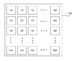
- FIG. 1 is a plan view of a camera array with a plurality of imagers, according to one embodiment.
- FIG. 2A is a perspective view of a camera array with lens elements, according to one embodiment.
- FIG. 2B is a cross-sectional view of a camera array, according to one embodiment.
- FIGS. 3A and 3B are sectional diagrams illustrating changes in the heights of lens elements depending on changes in the dimensions of imagers, according to one embodiment.
- FIG. 3C is a diagram illustrating chief ray angles varying depending on differing dimensions of the lens elements.
- FIG. 4 is a functional block diagram for an imaging device, according to one embodiment.
- FIG. 5 is a functional block diagram of an image processing pipeline module, according to one embodiment.
- FIGS. 6A through 6E are plan views of camera arrays having different layouts of heterogeneous imagers, according to embodiments.
- FIG. 7 is a flowchart illustrating a process of generating an enhanced image from lower resolution images captured by a plurality of imagers, according to one embodiment.
- Embodiments relate to using a distributed approach to capturing images using a plurality of imagers of different imaging characteristics.
- Each imager may be spatially shifted from another imager in such a manner that an imager captures an image that us shifted by a sub-pixel amount with respect to another imager captured by another imager.
- Each imager may also include separate optics with different filters and operate with different operating parameters (e.g., exposure time). Distinct images generated by the imagers are processed to obtain an enhanced image.
- Each imager may be associated with an optical element fabricated using wafer level optics (WLO) technology.
- WLO wafer level optics
- a sensor element or pixel refers to an individual light sensing element in a camera array.
- the sensor element or pixel includes, among others, traditional CIS (CMOS Image Sensor), CCD (charge-coupled device), high dynamic range pixel, multispectral pixel and various alternatives thereof.
- An imager refers to a two dimensional array of pixels.
- the sensor elements of each imager have similar physical properties and receive light through the same optical component. Further, the sensor elements in the each imager may be associated with the same color filter.
- a camera array refers to a collection of imagers designed to function as a unitary component.
- the camera array may be fabricated on a single chip for mounting or installing in various devices.
- An array of camera array refers to an aggregation of two or more camera arrays. Two or more camera arrays may operate in conjunction to provide extended functionality over a single camera array.
- Image characteristics of an imager refer to any characteristics or parameters of the imager associated with capturing of images.
- the imaging characteristics may include, among others, the size of the imager, the type of pixels included in the imager, the shape of the imager, filters associated with the imager, the exposure time of the imager, aperture size associated with the imager, the configuration of the optical element associated with the imager, gain of the imager, the resolution of the imager, and operational timing of the imager.
- FIG. 1 is a plan view of a camera array 100 with imagers 1 A through NM, according to one embodiment.
- the camera array 100 is fabricated on a semiconductor chip to include a plurality of imagers 1 A through NM.
- Each of the imagers 1 A through NM may include a plurality of pixels (e.g., 0.32 Mega pixels).
- the imagers 1 A through NM are arranged into a grid format as illustrated in FIG. 1 .
- the imagers are arranged in a non-grid format.
- the imagers may be arranged in a circular pattern, zigzagged pattern or scattered pattern.
- the camera array may include two or more types of heterogeneous imagers, each imager including two or more sensor elements or pixels. Each one of the imagers may have different imaging characteristics. Alternatively, there may be two or more different types of imagers where the same type of imagers shares the same imaging characteristics.
- each imager 1 A through NM has its own filter and/or optical element (e.g., lens).
- each of the imagers 1 A through NM or a group of imagers may be associated with spectral color filters to receive certain wavelengths of light.
- Example filters include a traditional filter used in the Bayer pattern (R, G, B or their complements C, M, Y), an IR-cut filter, a near-IR filter, a polarizing filter, and a custom filter to suit the needs of hyper-spectral imaging.
- Some imagers may have no filter to allow reception of both the entire visible spectra and near-IR, which increases the imager's signal-to-noise ratio.
- the number of distinct filters may be as large as the number of imagers in the camera array. Further, each of the imagers 1 A through NM or a group of imagers may receive light through lens having different optical characteristics (e.g., focal lengths) or apertures of different sizes.
- the camera array includes other related circuitry.
- the other circuitry may include, among others, circuitry to control imaging parameters and sensors to sense physical parameters.
- the control circuitry may control imaging parameters such as exposure times, gain, and black level offset.
- the sensor may include dark pixels to estimate dark current at the operating temperature. The dark current may be measured for on-the-fly compensation for any thermal creep that the substrate may suffer from.
- the circuit for controlling imaging parameters may trigger each imager independently or in a synchronized manner.
- the start of the exposure periods for the various imagers in the camera array (analogous to opening a shutter) may be staggered in an overlapping manner so that the scenes are sampled sequentially while having several imagers being exposed to light at the same time.
- the exposure time per sample is limited to 1/N seconds. With a plurality of imagers, there is no such limit to the exposure time per sample because multiple imagers may be operated to capture images in a staggered manner.
- Each imager can be operated independently. Entire or most operations associated with each individual imager may be individualized.
- a master setting is programmed and deviation (i.e., offset or gain) from such master setting is configured for each imager.
- the deviations may reflect functions such as high dynamic range, gain settings, integration time settings, digital processing settings or combinations thereof. These deviations can be specified at a low level (e.g., deviation in the gain) or at a higher level (e.g., difference in the ISO number, which is then automatically translated to deltas for gain, integration time, or otherwise as specified by context/master control registers) for the particular camera array.
- the parameters for the imagers are arbitrarily fixed for a target application. In another embodiment, the parameters are configured to allow a high degree of flexibility and programmability.
- the camera array is designed as a drop-in replacement for existing camera image sensors used in cell phones and other mobile devices.
- the camera array may be designed to be physically compatible with conventional image sensors of approximately the same resolution although the achieved resolution of the camera array may exceed conventional image sensors in many photographic situations.
- the camera array of the embodiment may include fewer pixels to obtain equal or better quality images compared to conventional image sensors.
- the size of the pixels in the imager may be reduced compared to pixels in conventional image sensors while achieving comparable results.
- the logic overhead for the individual imagers is preferably constrained in the silicon area.
- much of the pixel control logic is a single collection of functions common to all or most of the imagers with a smaller set of functions applicable each imager.
- the conventional external interface for the imager may be used because the data output does not increase significantly for the imagers.
- the camera array including the imagers replaces a conventional image sensor of M megapixels.
- the camera array includes N ⁇ N imagers, each sensor including pixels of
- Each imager in the camera array also has the same aspect ratio as the conventional image sensor being replaced.
- Table 1 lists example configurations of camera arrays according to the present invention replacing conventional image sensor.
- the Super-Resolution Factors in Table 1 are estimates and the Effective Resolution values may differ based on the actual Super-Resolution factors achieved by processing.
- the number of imagers in the camera array may be determined based on, among other factors, (i) resolution, (ii) parallax, (iii) sensitivity, and (iv) dynamic range.
- a first factor for the size of imager is the resolution. From a resolution point of view, the preferred number of the imagers ranges from 2 ⁇ 2 to 6 ⁇ 6 because an array size of larger than 6 ⁇ 6 is likely to destroy frequency information that cannot be recreated by the super-resolution process. For example, 8 Megapixel resolution with 2 ⁇ 2 imager will require each imager to have 2 Megapixels. Similarly, 8 Megapixel resolution with a 5 ⁇ 5 array will require each imager to have 0.32 Megapixels.
- a second factor that may constrain the number of imagers is the issue of parallax and occlusion.
- the portion of the background scene that is occluded from the view of the imager is called as “occlusion set.”
- occlusion set the portion of the background scene that is occluded from the view of the imager.
- the occlusion set of each imager is different.
- a third factor that may put a lower bound on the number of imagers is the issue of sensitivity in low light conditions.
- imagers for detecting near-IR spectrum may be needed.
- the number of imagers in the camera array may need to be increased to accommodate such near-IR imagers.
- a fourth factor in determining the size of the imager is dynamic range.
- To provide dynamic range in the camera array it is advantageous to provide several imagers of the same filter type (chroma or luma). Each imager of the same filter type may then be operated with different exposures simultaneously. The images captured with different exposures may be processed to generate a high dynamic range image.
- the preferred number of imagers is 2 ⁇ 2 to 6 ⁇ 6.
- 4 ⁇ 4 and 5 ⁇ 5 configurations are more preferable than 2 ⁇ 2 and 3 ⁇ 3 configurations because the former are likely to provide sufficient number of imagers to resolve occlusion issues, increase sensitivity and increase the dynamic range.
- the computational load required to recover resolution from these array sizes will be modest in comparison to that required in the 6 ⁇ 6 array.
- Arrays larger than 6 ⁇ 6 may, however, be used to provide additional features such as optical zooming and multispectral imaging.
- the information from the near-IR images is added to the resolution captured by the luma imagers.
- at least 50% of the imagers may be used for sampling the luma and/or near-IR spectra.
- 4 imagers samples luma
- 4 imagers samples near-IR
- the remaining 8 imagers samples two chroma (Red and Blue).
- 9 imagers samples luma, 8 imagers samples near-IR
- the remaining 8 imagers samples two chroma (Red and Blue).
- the imagers with these filters may be arranged symmetrically within the camera array to address occlusion due to parallax.
- the imagers in the camera array are spatially separated from each other by a predetermined distance.
- the parallax between the images captured by the imagers may be increased.
- the increased parallax is advantageous where more accurate distance information is important.
- Separation between two imagers may also be increased to approximate the separation of a pair of human eyes. By approximating the separation of human eyes, a realistic stereoscopic 3D image may be provided to present the resulting image on an appropriate 3D display device.
- multiple camera arrays are provided at different locations on a device to overcome space constraints.
- One camera array may be designed to fit within a restricted space while another camera array may be placed in another restricted space of the device. For example, if a total of 20 imagers are required but the available space allows only a camera array of 1 ⁇ 10 imagers to be provided on either side of a device, two camera arrays each including 10 imagers may be placed on available space at both sides of the device.
- Each camera array may be fabricated on a substrate and be secured to a motherboard or other parts of a device. The images collected from multiple camera arrays may be processed to generate images of desired resolution and performance.
- a design for a single imager may be applied to different camera arrays each including other types of imagers.
- Other variables in the camera array such as spatial distances, color filters and combination with the same or other sensors may be modified to produce a camera array with differing imaging characteristics. In this way, a diverse mix of camera arrays may be produced while maintaining the benefits from economies of scale.
- the camera array employs wafer level optics (WLO) technology.
- WLO is a technology that molds optics on glass wafers followed by packaging of the optics directly with the imager into a monolithic integrated module.
- the WLO procedure may involve, among other procedures, using a diamond-turned mold to create each plastic lens element on a glass substrate.
- FIG. 2A is a perspective view of a camera array assembly 200 with wafer level optics 210 and a camera array 230 , according to one embodiment.
- the wafer level optics 210 includes a plurality of lens elements 220 , each lens element 220 covering one of twenty-five imagers 240 in the camera array 230 .
- the camera array assembly 200 has an array of smaller lens elements occupy much less space compared to a single large lens covering the entire camera array 230 .
- FIG. 2B is a sectional view of a camera array assembly 250 , according to one embodiment.
- the camera assembly 250 includes a top lens wafer 262 , a bottom lens wafer 268 , a substrate 278 with multiple imagers formed thereon and spacers 258 , 264 270 .
- the camera array assembly 250 is packaged within an encapsulation 254 .
- a top spacer 258 is placed between the encapsulation 254 and the top lens wafer 262 .
- Multiple optical elements 288 are formed on the top lens wafer 262 .
- a middle spacer 264 is placed between the top lens wafer 262 and a bottom lens wafer 268 .
- Another set of optical elements 286 is formed on the bottom lens wafer 268 .
- a bottom spacer 270 is placed between the bottom lens wafer 268 and the substrate 278 .
- Through-silicon vias 274 are also provided to paths for transmitting signal from the imagers.
- the top lens wafer 262 may be partially coated with light blocking materials 284 (e.g., chromium) to block of light.
- the portions of the top lens wafer 262 not coated with the blocking materials 284 serve as apertures through which light passes to the bottom lens wafer 268 and the imagers.
- filters 282 are formed on the bottom lens wafer 268 .
- Light blocking materials 280 e.g., chromium
- the bottom surface of the surface is covered with a backside redistribution layer (“RDL”) and solder balls 276 .
- RDL backside redistribution layer
- the camera array assembly 250 includes 5 ⁇ 5 array of imagers.
- the camera array 250 has a width W of 7.2 mm, and a length of 8.6 mm.
- Each imager in the camera array may have a width S of 1.4 mm.
- the total height t 1 of the optical components is approximately 1.26 mm and the total height t 2 the camera array assembly is less than 2 mm.
- FIGS. 3A and 3B are diagrams illustrating changes in the height t of a lens element pursuant to changes in dimensions in an x-y plane.
- a lens element 320 in FIG. 3B is scaled by 1/n compared to a lens element 310 in FIG. 3A .
- the diameter L/n of the lens element 320 is smaller than the diameter L by a factor of n
- the height tin of the lens element 320 is also smaller than the height t of the lens element 310 by a factor of n.
- the reduced height of the camera array assembly may be used to design less aggressive lenses having better optical properties such as improved chief ray angle, reduced distortion, and improved color aberration.
- FIG. 3C illustrates improving a chief ray angle (CRA) by reducing the thickness of the camera array assembly.
- CRA 1 is the chief ray angle for a single lens covering an entire camera array.
- the chief ray angle can be reduced by increasing the distance between the camera array and the lens, the thickness constraints imposes constraints on increasing the distance.
- the CRA 1 for camera array having a single lens element is large, resulting in reduced optical performance.
- CRA 2 is the chief ray angle for an imager in the camera array that is scaled in thickness as well as other dimensions. The CRA 2 remains the same as the CRA 1 of the conventional camera array and results in no improvement in the chief ray angle.
- the chief ray angle CRA 3 in the camera array assembly may be reduced compared to CRA 1 or CRA 2 , resulting in better optical performance.
- the camera arrays according to the present invention has reduced thickness requirements, and therefore, the distance of the lens element and the camera array may be increased to improve the chief ray angle.
- each lens element is subject to less rigorous design constraints yet produces better or equivalent performance compared to conventional lens element covering a wide light spectrum because each lens element may be designed to direct a narrow band of light.
- an imager receiving visible or near-IR spectrum may have a lens element specifically optimized for this spectral band of light.
- the lens element may have differing focal lengths so that the focal plane is the same for different spectral bands of light. The matching of the focal plane across different wavelengths of light increases the sharpness of image captured at the imager and reduces longitudinal chromatic aberration.
- lens element advantages include, among others, reduced cost, reduced amount of materials, and the reduction in the manufacturing steps.
- the wafer size for producing the lens element may also be reduced. This reduces the cost and the amount of materials considerably. Further, the number of lens substrate is reduced, which results in reduced number of manufacturing steps and reduced attendant yield costs.
- the placement accuracy required to register the lens array to the imagers is typically no more stringent than in the case of a conventional imager because the pixel size for the camera array according to the present invention may be substantially same as a conventional image sensor.
- the WLO fabrication process includes: (i) incorporating lens element stops by plating the lens element stops onto the substrate before lens molding, and (ii) etching holes in the substrate and performing two-sided molding of lenses through the substrate.
- the etching of holes in the substrate is advantageous because index mismatch is not caused between plastic and substrate. In this way, light absorbing substrate that forms natural stops for all lens elements (similar to painting lens edges black) may be used.
- filters are part of the imager. In another embodiment, filters are part of a WLO subsystem.
- FIG. 4 is a functional block diagram illustrating an imaging system 400 , according to one embodiment.
- the imaging system 400 may include, among other components, the camera array 410 , an image processing pipeline module 420 and a controller 440 .
- the camera array 410 includes two or more imagers, as described above in detail with reference to FIGS. 1 and 2 . Images 412 are captured by the two or more imagers in the camera array 410 .
- the controller 440 is hardware, software, firmware or a combination thereof for controlling various operation parameters of the camera array 410 .
- the controller 440 receives inputs 446 from a user or other external components and sends operation signals 442 to control the camera array 410 .
- the controller 440 may also send information 444 to the image processing pipeline module 420 to assist processing of the images 412 .
- the image processing pipeline module 420 is hardware, firmware, software or a combination for processing the images received from the camera array 410 .
- the image processing pipeline module 420 processes multiple images 412 , for example, as described below in detail with reference to FIG. 5 .
- the processed image 422 is then sent for display, storage, transmittal or further processing.
- FIG. 5 is a functional block diagram illustrating the image processing pipeline module 420 , according to one embodiment.
- the image processing pipeline module 420 may include, among other components, an upstream pipeline processing module 510 , an image pixel correlation module 514 , a parallax confirmation and measurement module 518 , a parallax compensation module 522 , a super-resolution module 526 , an address conversion module 530 , an address and phase offset calibration module 554 , and a downstream color processing module 564 .
- the address and phase offset calibration module 554 is a storage device for storing calibration data produced during camera array characterization in the manufacturing process or a subsequent recalibration process.
- the calibration data indicates mapping between the addresses of physical pixels 572 in the imagers and the logical addresses 546 , 548 of an image.
- the address conversion module 530 performs normalization based on the calibration data stored in the address and phase offset calibration module 554 . Specifically, the address conversion module 530 converts “physical” addresses of the individual pixels in the image to “logical” addresses 548 of the individual pixels in the imagers or vice versa. In order for super-resolution processing to produce an image of enhanced resolution, the phase difference between corresponding pixels in the individual imagers needs to be resolved. The super-resolution process may assume that for each pixel in the resulting image the set of input pixels from each of the imager is consistently mapped and that the phase offset for each imager is already known with respect to the position of the pixel in the resulting image. The address conversion module 530 resolves such phase differences by converting the physical addresses in the images 412 into logical addresses 548 of the resulting image for subsequent processing.
- the images 412 captured by the imagers 540 are provided to the upstream pipeline processing module 510 .
- the upstream pipe processing module 510 may perform one or more of Black Level calculation and adjustments, fixed noise compensation, optical PSF (point spread function) deconvolution, noise reduction, and crosstalk reduction.
- an image pixel correlation module 514 performs calculation to account for parallax that becomes more apparent as objects being captured approaches to the camera array. Specifically, the image pixel correlation module 514 aligns portions of images captured by different imagers to compensate for the parallax.
- the image pixel correlation module 514 compares the difference between the average values of neighboring pixels with a threshold and flags the potential presence of parallax when the difference exceeds the threshold.
- the threshold may change dynamically as a function of the operating conditions of the camera array. Further, the neighborhood calculations may also be adaptive and reflect the particular operating conditions of the selected imagers.
- parallax detection is accomplished by a running pixel correlation monitor. This operation takes place in logical pixel space across the imagers with similar integration time conditions. When the scene is at practical infinity, the data from the imagers is highly correlated and subject only to noise-based variations. When an object is close enough to the camera, however, a parallax effect is introduced that changes the correlation between the imagers. Due to the spatial layout of the imagers, the nature of the parallax-induced change is consistent across all imagers.
- the correlation difference between any pair of imagers dictates the difference between any other pair of imagers and the differences across the other imagers.
- This redundancy of information enables highly accurate parallax confirmation and measurement by performing the same or similar calculations on other pairs of imagers. If parallax is present in the other pairs, the parallax should occur at roughly the same physical location of the scene taking into account the positions of the imagers.
- the measurement of the parallax may be accomplished at the same time by keeping track of the various pair-wise measurements and calculating an “actual” parallax difference as a least squares (or similar statistic) fit to the sample data.
- Other methods for detecting the parallax may include detecting and tracking vertical and horizontal high-frequency image elements from frame-to-frame.
- the parallax compensation module 522 processes images including objects close enough to the camera array to induce parallax differences larger than the accuracy of the phase offset information required by super resolution process.
- the parallax compensation module 522 uses the scan-line based parallax information generated in the parallax detection and measurement module 518 to further adjust mapping between physical pixel addresses and logical pixel addresses before the super-resolution process. There are two cases that occur during this processing. In a more common case, addressing and offsetting adjustment are required when the input pixels have shifted positions relative to the image-wise-corresponding pixels in other imagers. In this case, no further processing with respect to parallax is required before performing super-resolution.
- a pixel or group of pixels are shifted in such a way that exposes the occlusion set.
- the parallax compensation process generates tagged pixel data indicating that the pixels of the occlusion set should not be considered in the super-resolution process.
- the parallax information 524 is sent to the address conversion module 530 .
- the address conversion module 530 uses the parallax information 524 along with the calibration data 558 from the address and phase offset calibration module 554 to determine the appropriate X and Y offsets to be applied to logical pixel address calculations.
- the address conversion module 530 also determines the associated sub-pixel offset for a particular imager pixel with respect to pixels in the resulting image 428 produced by the super-resolution process.
- the address conversion module 530 takes into account the parallax information 524 and provides logical addresses 546 accounting for the parallax.
- the image is processed by the super-resolution module 526 to obtain a high resolution synthesized image 422 from low resolution images, as described below in detail.
- the synthesized image 422 may then be fed to the downstream color processing module 564 to perform one or more of the following operations: focus recover, white balance, color correction, gamma correction, RGB to YUV correction, edge-aware sharpening, contrast enhancement and compression.
- the image processing pipeline module 420 may include components for additional processing of the image.
- the image processing pipeline module 420 may include a correction module for correcting abnormalities in images caused by a single pixel defect or a cluster of pixel defects.
- the correction module may be embodied on the same chip as the camera array, as a component separate from the camera array or as a part of the super-resolution module 526 .
- the super-resolution module 526 generates a higher resolution synthesized image by processing low resolution images captured by the imagers 540 .
- the overall image quality of the synthesized image is higher than images captured from any one of the imagers individually.
- the individual imagers operate synergistically, each contributing to higher quality images using their ability to capture a narrow part of the spectrum without sub-sampling.
- W k represents the contribution of the HR scene (x) (via blurring, motion, and sub-sampling) to each of the LR images (y k ) captured on each of the k imagers and n k is the noise contribution.
- FIGS. 6A through 6E illustrate various configurations of imagers for obtaining a high resolution image through a super-resolution process, according to embodiments of the present invention.
- R represents an imager having a red filter
- G represents a imager having a green filter
- B represents an imager having a blue filter
- P represents a polychromatic imager having sensitivity across the entire visible spectra and near-IR spectrum
- I represents an imager having a near-IR filter.
- the polychromatic imager may sample image from all parts of the visible spectra and the near-IR region (i.e., from 650 nm to 800 nm). In the embodiment of FIG.
- the center columns and rows of the imagers include polychromatic imagers.
- the remaining areas of the camera array are filled with imagers having green filters, blue filters, and red filters.
- the embodiment of FIG. 6A does not include any imagers for detecting near-IR spectrum alone.
- the embodiment of FIG. 6B has a configuration similar to conventional Bayer filter mapping. This embodiment does not include any polychromatic imagers or near-IR imagers. As described above in detail with reference to FIG. 1 , the embodiment of FIG. 6B is different from conventional Bayer filter configuration in that each color filter is mapped to each imager instead of being mapped to an individual pixel.
- FIG. 6C illustrates an embodiment where the polychromatic imagers form a symmetric checkerboard pattern.
- FIG. 6D illustrates an embodiment where four near-IR imagers are provided.
- FIG. 6E illustrates an embodiment with irregular mapping of imagers.
- the embodiments of FIGS. 6A through 6E are merely illustrative and various other layouts of imagers can also be used.
- polychromatic imagers and near-IR imagers are advantageous because these sensors may capture high quality images in low lighting conditions.
- the images captured by the polychromatic imager or the near-IR imager are used to denoise the images obtained from regular color imagers.
- the premise of increasing resolution by aggregating multiple low resolution images is based on the fact that the different low resolution images represent slightly different viewpoints of the same scene. If the LR images are all shifted by integer units of a pixel, then each image contains essentially the same information. Therefore, there is no new information in LR images that can be used to create the HR image.
- the layout of the imagers may be preset and controlled so that each imager in a row or a column is a fixed sub-pixel distance from its neighboring imagers. The wafer level manufacturing and packaging process allows accurate formation of imagers to attain the sub-pixel precisions required for the super-resolution processing.
- An issue of separating the spectral sensing elements into different imagers is parallax caused by the physical separation of the imagers.
- the imagers are symmetrically placed, at least two imagers can capture the pixels around the edge of a foreground object. In this way, the pixels around the edge of a foreground object may be aggregated to increase resolution as well as avoiding any occlusions.
- Another issue related to parallax is the sampling of color. The issue of sampling the color may be reduced by using parallax information in the polychromatic imagers to improve the accuracy of the sampling of color from the color filtered imagers.
- near-IR imagers are used to determine relative luminance differences compared to a visible spectra imager.
- Objects have differing material reflectivity results in differences in the images captured by the visible spectra and the near-IR spectra.
- the near-IR imager exhibits a higher signal to noise ratios. Therefore, the signals from the near-IR sensor may be used to enhance the luminance image.
- the transferring of details from the near-IR image to the luminance image may be performed before aggregating spectral images from different imagers through the super-resolution process. In this way, edge information about the scene may be improved to construct edge-preserving images that can be used effectively in the super-resolution process.
- the advantage of using near-IR imagers is apparent from equation (2) where any improvement in the estimate for the noise (i.e., n) leads to a better estimate of the original HR scene (x).
- FIG. 7 is a flowchart illustrating a process of generating an HR image from LR images captured by a plurality of imagers, according to one embodiment.
- luma images, near-IR images and chroma images are captured 710 by imagers in the camera array.
- normalization is performed 714 on the captured images to map physical addresses of the imagers to logical addresses in the enhanced image.
- Parallax compensation is then performed 720 to resolve any differences in the field-of-views of the imagers due to spatial separations between the imagers.
- Super-resolution processing is then performed 724 to obtain super-resolved luma images, super-resolved near-IR images, and super-resolved chroma images.
- the process proceeds to normalize 730 a super-resolved near-IR image with respect to a super-resolved luma image.
- a focus recovery is then performed 742 .
- the focus recovery is performed 742 using PSF (point spread function) deblurring per each channel.
- the super-resolution is processed 746 based on near-IR images and the luma images.
- a synthesized image is then constructed 750 .
- the super-resolved near-IR images and luma images are aligned 734 . Then the super-resolved luma images are denoised 738 using the near-IR super-resolved images. Then the process proceeds to performing focus recovery 742 and repeats the same process as when the lighting condition is better than the preset parameter. Then the process terminates.
- CMOS imagers typically very good in the near-IR regions covering 650 nm to 800 nm and reasonably good between 800 nm and 1000 nm.
- near-IR images having no chroma information information in this spectral region is useful in low lighting conditions because the near-IR images are relatively free of noise.
- the near-IR images may be used to denoise color images under the low lighting conditions.
- an image from a near-IR imager is fused with another image from a visible light imager.
- a registration is performed between the near-IR image and the visible light image to resolve differences in viewpoints.
- the registration process may be performed in an offline, one-time, processing step.
- the luminance information on the near-IR image is interpolated to grid points that correspond to each grid point on the visible light image.
- denoising and detail transfer process may be performed.
- the denoising process allows transfer of signal information from the near-IR image to the visible light image to improve the overall SNR of the fusion image.
- the detail transfer ensures that edges in the near-IR image and the visible light image are preserved and accentuated to improve the overall visibility of objects in the fused image.
- a near-IR flash may serve as a near-IR light source during capturing of an image by the near-IR imagers.
- Using the near-IR flash is advantageous, among other reasons, because (i) the harsh lighting on objects of interest may be prevented, (ii) ambient color of the object may be preserved, and (iii) red-eye effect may be prevented.
- a visible light filter that allows only near-IR rays to pass through is used to further optimize the optics for near-IR imaging.
- the visible light filter improves the near-IR optics transfer function because the light filter results in sharper details in the near-IR image.
- the details may then be transferred to the visible light images using a dual bilateral filter as described, for example, in Eric P. Bennett et al., “Multispectral Video Fusion,” Computer Graphics (ACM SIGGRAPH Proceedings) (Jul. 25, 2006), which is incorporated by reference herein in its entirety.
- An auto-exposure (AE) algorithm is important to obtaining an appropriate exposure for the scene to be captured.
- the design of the AE algorithm affects the dynamic range of captured images.
- the AE algorithm determines an exposure value that allows the acquired image to fall in the linear region of the camera array's sensitivity range. The linear region is preferred because a good signal-to-noise ratio is obtained in this region. If the exposure is too low, the picture becomes under-saturated while if the exposure is too high the picture becomes over-saturated.
- an iterative process is taken to reduce the difference between measured picture brightness and previously defined brightness below a threshold. This iterative process requires a large amount of time for convergence, and sometimes results in an unacceptable shutter delay.
- the picture brightness of images captured by a plurality of imagers is independently measured.
- a plurality of imagers are set to capturing images with different exposures to reduce the time for computing the adequate exposure.
- each of the imagers may be set with different exposures.
- the near-IR imagers are used to capture low-light aspects of the scene and the luma imagers are used to capture the high illumination aspects of the scene. This results in a total of 17 possible exposures. If exposure for each imager is offset from an adjacent imager by a factor of 2, for example, a maximum dynamic range of 2 17 or 102 dB can be captured. This maximum dynamic range is considerably higher than the typical 48 dB attainable in a conventional camera with 8 bit image outputs.
- the responses (under-exposed, over-exposed or optimal) from each of the multiple imagers are analyzed based on how many exposures are needed at the subsequent time instant.
- the ability to query multiple exposures simultaneously in the range of possible exposures accelerates the search compared to the case where only one exposure is tested at once. By reducing the processing time for determining the adequate exposure, shutter delays and shot-to-shot lags may be reduced.
- the HDR image is synthesized from multiple exposures by combining the images after linearizing the imager response for each exposure.
- the images from the imagers may be registered before combining to account for the difference in the viewpoints of the imagers.
- At least one imager includes HDR pixels to generate HDR images.
- HDR pixels are specialized pixels that capture high dynamic range scenes. Although HDR pixels show superior performances compared to other pixels, HDR pixels show poor performance at low lighting conditions in comparison with near-IR imagers. To improve performance at low lighting conditions, signals from the near-IR imagers may be used in conjunction with the signal from the HDR imager to attain better quality images across different lighting conditions.
- an HDR image is obtained by processing images captured by multiple imagers by processing, as disclosed, for example, in Paul Debevec et al., “Recovering High Dynamic Range Radiance Maps from Photographs,” Computer Graphics (ACM SIGGRAPH Proceedings), (Aug. 16, 1997), which is incorporated by reference herein in its entirety.
- the ability to capture multiple exposures simultaneously using the imager is advantageous because artifacts caused by motion of objects in the scene can be mitigated or eliminated.
- a multi-spectral image is rendered by multiple imagers to facilitate the segmentation or recognition of objects in a scene.
- the spectral reflectance coefficients may be estimated by capturing the scene in multiple spectral dimensions using imagers with different color filters and analyzing the captured images using Principal Components Analysis (PCA).
- PCA Principal Components Analysis
- half of the imagers in the camera array are devoted to sampling in the basic spectral dimensions (R, G, and B) and the other half of the imagers are devoted to sampling in a shifted basic spectral dimensions (R′, G′, and B′).
- the shifted basic spectral dimensions are shifted from the basic spectral dimensions by a certain wavelength (e.g., 10 nm).
- pixel correspondence and non-linear interpolation is performed to account for the sub-pixel shifted views of the scene.
- the spectral reflectance coefficients of the scene are synthesized using a set of orthogonal spectral basis functions as disclosed, for example, in J. P. S. Parkkinen, J. Hallikainen and T. Jaaskelainen, “Characteristic Spectra of Munsell Colors,” J. Opt. Soc. Am., A 6:318 (August 1989), which is incorporated by reference herein in its entirety.
- the basis functions are eigenvectors derived by PCA of a correlation matrix and the correlation matrix is derived from a database storing spectral reflectance coefficients measured by, for example, Munsell color chips (a total of 1257) representing the spectral distribution of a wide range of real world materials to reconstruct the spectrum at each point in the scene.
- each sampling grid of each imager is offset by a sub-pixel shift from the others.
- no two sampling grid of the imager overlap. That is, the superposition of all the sampling grids from all the imagers forms a dense, possibly non-uniform, montage of points.
- Scattered data interpolation methods may be used to determine the spectral density at each sample point in this non-uniform montage for each spectral image, as described, for example, in Shiaofen Fang et al., “Volume Morphing Methods for Landmark Based 3D Image Deformation” by SPIE vol. 2710, proc. 1996 SPIE Intl Symposium on Medical Imaging, page 404-415, Newport Beach, Calif. (February 1996), which is incorporated by reference herein in its entirety. In this way, a certain amount of resolution lost in the process of sampling the scene using different spectral filters may be recovered.
- image segmentation and object recognition are facilitated by determining the spectral reflectance coefficients of the object.
- a network of cameras is used to track an object as it moves from the operational zone of one camera to another.
- Each zone may have its own unique lighting conditions (fluorescent, incandescent, D65, etc.) that may cause the object to have a different appearance in each image captured by different cameras. If these cameras capture the images in a hyper-spectral mode, all images may be converted to the same illuminant to enhance object recognition performance.
- camera arrays with multiple imagers are used for providing medical diagnostic images.
- Full spectral digitized images of diagnostic samples contribute to accurate diagnosis because doctors and medical personnel can place higher confidence in the resulting diagnosis.
- the imagers in the camera arrays may be provided with color filters to provide full spectral data.
- Such camera array may be installed on cell phones to capture and transmit diagnostic information to remote locations as described, for example, in Andres W. Martinez et al., “Simple Telemedicine for Developing Regions: Camera Phones and Paper-Based Microfluidic Devices for Real-Time, Off-Site Diagnosis,” Analytical Chemistry (American Chemical Society) (Apr. 11, 2008), which is incorporated by reference herein in its entirety.
- the camera arrays including multiple imagers may provide images with a large depth of field to enhance the reliability of image capture of wounds, rashes, and other symptoms.
- a small imager (including, for example, 20-500 pixels) with a narrow spectral bandpass filters is used to produce a signature of the ambient and local light sources in a scene.
- the spectral bandpass filters may be ordinary color filters or diffractive elements of a bandpass width adequate to allow the number of camera arrays to cover the visible spectrum of about 400 nm.
- These imagers may run at a much higher frame rate and obtain data (which may or may not be used for its pictorial content) for processing into information to control the exposure and white balance of other larger imagers in the same camera array.
- the small imagers may also be interspersed within the camera array.
- a subset of imagers in the camera array includes telephoto lenses.
- the subset of imagers may have other imaging characteristics same as imagers with non-telephoto lenses. Images from this subset of imagers are combined and super-resolution processed to form a super-resolution telephoto image.
- the camera array includes two or more subsets of imagers equipped with lenses of more than two magnifications to provide differing zoom magnifications.
- Embodiments of the camera arrays may achieve its final resolution by aggregating images through super-resolution. Taking an example of providing 5 ⁇ 5 imagers with a 3 ⁇ optical zoom feature, if 17 imagers are used to sample the luma (G) and 8 imagers are used to sample the chroma (R and B), 17 luma imagers allow a resolution that is four times higher than what is achieved by any single imager in the set of 17 imagers. If the number of the imager is increased from 5 ⁇ 5 to 6 ⁇ 6, an addition of 11 extra imagers becomes available.
- a resolution that is 60% of the conventional image sensor is achieved when 8 of the additional 11 imagers are dedicated to sampling luma (G) and the remaining 3 imagers are dedicated to chroma (R and B) and near-IR sampling at 3 ⁇ zoom.
- the reduced chroma to luma sampling ratio is somewhat offset by using the super-resolved luma image at 3 ⁇ zoom as a recognition prior on the chroma (and near-IR) image to resample the chroma image at a higher resolution.
- a resolution equivalent to the resolution of conventional image sensor is achieved at 1 ⁇ zoom.
- a resolution equivalent to about 60% of conventional image sensor outfitted with a 3 ⁇ zoom lens is obtained by the same imagers.
- the decreased luma resolution is offset by the fact that the optics of conventional image sensor has reduced efficiency at 3 ⁇ zoom due to crosstalk and optical aberrations.
- the zoom operation achieved by multiple imagers has the following advantages.
- optical aberrations and field curvature must be corrected across the whole operating range of the lens, which is considerably harder in a zoom lens with moving elements than in a fixed lens element where only aberrations for a fixed focal length need to be corrected.
- the fixed lens in the imagers has a fixed chief ray angle for a given height, which is not the case with conventional image sensor with a moving zoom lens.
- the imagers allow simulation of zoom lenses without significantly increasing the optical track height. The reduced height allows implementation of thin modules even for camera arrays with zooming capability.
- the pixels in the images are mapped onto an output image with a size and resolution corresponding to the amount of zoom desired in order to provide a smooth zoom capability from the widest-angle view to the greatest-magnification view.
- the image information available is such that a center area of the image has a higher resolution available than the outer area.
- nested regions of different resolution may be provided with resolution increasing toward the center.
- An image with the most telephoto effect has a resolution determined by the super-resolution ability of the imagers equipped with the telephoto lenses.
- An image with the widest field of view can be formatted in at least one of two following ways. First, the wide field image may be formatted as an image with a uniform resolution where the resolution is determined by the super-resolution capability of the set of imagers having the wider-angle lenses. Second, the wide field image is formatted as a higher resolution image where the resolution of the central part of the image is determined by the super-resolution capability of the set of imagers equipped with telephoto lenses. In the lower resolution regions, information from the reduced number of pixels per image area is interpolated smoothly across the larger number of “digital” pixels. In such an image, the pixel information may be processed and interpolated so that the transition from higher to lower resolution regions occurs smoothly.
- zooming is achieved by inducing a barrel-like distortion into some, or all, of the array lens so that a disproportionate number of the pixels are dedicated to the central part of each image.
- every image has to be processed to remove the barrel distortion.
- pixels closer to the center are sub-sampled relative to outer pixels are super-sampled.
- zooming is performed, the pixels at the periphery of the imagers are progressively discarded and the sampling of the pixels nearer the center of the imager is increased.
- mipmap filters are built to allow images to be rendered at a zoom scale that is between the specific zoom range of the optical elements (e.g., 1 ⁇ and 3 ⁇ zoom scales of the camera array).
- Mipmaps are a precalculated optimized set of images that accompany a baseline image.
- a set of images associated with the 3 ⁇ zoom luma image can be created from a baseline scale at 3 ⁇ down to 1 ⁇ . Each image in this set is a version of the baseline 3 ⁇ zoom image but at a reduced level of detail.
- Rendering an image at a desired zoom level is achieved using the mipmap by (i) taking the image at 1 ⁇ zoom, and computing the coverage of the scene for the desired zoom level (i.e., what pixels in the baseline image needs to be rendered at the requested scale to produce the output image), (ii) for each pixel in the coverage set, determine if the pixel is in the image covered by the 3 ⁇ zoom luma image, (iii) if the pixel is available in the 3 ⁇ zoom luma image, then choose the two closest mipmap images and interpolate (using smoothing filter) the corresponding pixels from the two mipmap images to produce the output image, and (iv) if the pixel is unavailable in the 3 ⁇ zoom luma image, then choose the pixel from the baseline 1 ⁇ luma image and scale up to the desired scale to produce the output pixel.
- smooth optical zoom may be simulated at any point between two given discrete levels (i.e., 1 ⁇ zoom and 3 ⁇ zoom).
- the camera array generates high frame image sequences.
- the imagers in the camera array can operate independently to capture images.
- the camera array may capture images at the frame rate up to N time (where N is the number of imagers).
- the frame period for each imager may overlap to improve operations under low-light conditions.
- a subset of imagers may operate in a synchronized manner to produce images of higher resolution. In this case, the maximum frame rate is reduced by the number of imagers operating in a synchronized manner.
- the high-speed video frame rates can enables slow-motion video playback at a normal video rate.
- two luma imagers green imagers or near-IR imagers
- two blue imagers and two green imagers are used to obtain high-definition 1080p images.
- the chroma imagers can be upsampled to achieve 120 frames/sec for 1080p video.
- the number of frame rates can be scaled up linearly.
- Standard-Definition (480p) operation a frame rate of 240 frames/sec may be achieved using the same camera array.
- Conventional imaging devices with a high-resolution image sensor use binning or skipping to capture lower resolution images (e.g., 1080p30, 720p30 and 480p30).
- binning rows and columns in the captured images are interpolated in the charge, voltage or pixel domains in order to achieve the target video resolutions while reducing the noise.
- skipping rows and columns are skipped in order to reduce the power consumption of the sensor. Both of these techniques result in reduced image quality.
- the imagers in the camera arrays are selectively activated to capture a video image.
- 9 imagers including one near-IR imager
- 6 imagers including one near-IR imager
- 4 imagers including one near-IR imager
- 480p 720 ⁇ 480 pixels
- the near-IR imager to capture video images is advantageous because the information from the near-IR imager may be used to denoise each video image.
- the camera arrays of embodiments exhibit excellent low-light sensitivity and can operate in extremely low-light conditions.
- super-resolution processing is performed on images from multiple imagers to obtain higher resolution video imagers. The noise-reduction characteristics of the super-resolution process along with fusion of images from the near-IR imager results in a very low-noise images.
- high-dynamic-range (HDR) video capture is enabled by activating more imagers. For example, in a 5 ⁇ 5 camera array operating in 1080p video capture mode, there are only 9 cameras active. A subset of the 16 cameras may be overexposed and underexposed by a stop in sets of two or four to achieve a video output with a very high dynamic range.
- the multiple imagers are used for estimating distance to an object in a scene. Since information regarding the distance to each point in an image is available in the camera array along with the extent in x and y coordinates of an image element, the size of an image element may be determined. Further, the absolute size and shape of physical items may be measured without other reference information. For example, a picture of a foot can be taken and the resulting information may be used to accurately estimate the size of an appropriate shoe.
- reduction in depth of field is simulated in images captured by the camera array using distance information.
- the camera arrays according to the present invention produce images with greatly increased depth of field. The long depth of field, however, may not be desirable in some applications.
- a particular distance or several distances may be selected as the “in best focus” distance(s) for the image and based on the distance (z) information from parallax information, the image can be blurred pixel-by-pixel using, for example, a simple Gaussian blur.
- the depth map obtained from the camera array is utilized to enable a tone mapping algorithm to perform the mapping using the depth information to guide the level, thereby emphasizing or exaggerating the 3D effect.
- apertures of different sizes are provided to obtain aperture diversity.
- the aperture size has a direct relationship with the depth of field.
- the aperture is generally made as large as possible to allow as much light to reach the camera array.
- Different imagers may receive light through apertures of different sizes. For imagers to produce a large depth of field, the aperture may be reduced whereas other imagers may have large apertures to maximize the light received.
- the camera array according to the present invention refocuses based on images captured from offsets in viewpoints. Unlike a conventional plenoptic camera, the images obtained from the camera array of the present invention do not suffer from the extreme loss of resolution.
- the camera array according to the present invention produces sparse data points for refocusing compared to the plenoptic camera. In order to overcome the sparse data points, interpolation may be performed to refocus data from the spare data points.
- each imager in the camera array has a different centroid. That is, the optics of each imager are designed and arranged so that the fields of view for each imager slightly overlap but for the most part constitute distinct tiles of a larger field of view. The images from each of the tiles are panoramically stitched together to render a single high-resolution image.
- camera arrays may be formed on separate substrates and mounted on the same motherboard with spatial separation.
- the lens elements on each imager may be arranged so that the corner of the field of view slightly encompasses a line perpendicular to the substrate.
- the fields of view will be four slightly overlapping tiles. This allows a single design of WLO lens array and imager chip to be used to capture different tiles of a panoramic image.
- one or more sets of imagers are arranged to capture images that are stitched to produce panoramic images with overlapping fields of view while another imager or sets of imagers have a field of view that encompasses the tiled image generated.
- This embodiment provides different effective resolution for imagers with different characteristics. For example, it may be desirable to have more luminance resolution than chrominance resolution. Hence, several sets of imagers may detect luminance with their fields of view panoramically stitched. Fewer imagers may be used to detect chrominance with the field of view encompassing the stitched field of view of the luminance imagers.
- the camera array with multiple imagers is mounted on a flexible motherboard such that the motherboard can be manually bent to change the aspect ratio of the image.
- a set of imagers can be mounted in a horizontal line on a flexible motherboard so that in the quiescent state of the motherboard, the fields of view of all of the imagers are approximately the same. If there are four imagers, an image with double the resolution of each individual imager is obtained so that details in the subject image that are half the dimension of details that can be resolved by an individual imager. If the motherboard is bent so that it forms part of a vertical cylinder, the imagers point outward.
- the width of the subject image is doubled while the detail that can be resolved is reduced because each point in the subject image is in the field of view of two rather than four imagers.
- the subject image is four times wider while the detail that can be resolved in the subject is further reduced.
- the images processed by the imaging system 400 may be previewed before or concurrently with saving of the image data on a storage medium such as a flash device or a hard disk.
- the images or video data includes rich light field data sets and other useful image information that were originally captured by the camera array. Other traditional file formats could also be used.
- the stored images or video may be played back or transmitted to other devices over various wired or wireless communication methods.
- tools are provided for users by a remote server.
- the remote server may function both as a repository and an offline processing engine for the images or video.
- applets mashed as part of popular photo-sharing communities such as Flikr, Picasaweb, Facebook etc. may allow images to be manipulated interactively, either individually or collaboratively.
- software plug-ins into image editing programs may be provided to process images generated by the imaging device 400 on computing devices such as desktops and laptops.
- modules described herein may comprise a general-purpose computer selectively activated or reconfigured by a computer program stored in the computer.
- a computer program may be stored in a computer readable storage medium, such as, but is not limited to, any type of disk including floppy disks, optical disks, CD-ROMs, magnetic-optical disks, read-only memories (ROMs), random access memories (RAMs), EPROMs, EEPROMs, magnetic or optical cards, application specific integrated circuits (ASICs), or any type of media suitable for storing electronic instructions, and each coupled to a computer system bus.
- the computers referred to in the specification may include a single processor or may be architectures employing multiple processor designs for increased computing capability.
Abstract
Description
Typically, the noise level in the captured image influences the floor of the dynamic range. Thus, for an 8 bit image, the best case would be 48 dB assuming the RMS noise level is 1 bit. In reality, however, the RMS noise levels are higher than 1 bit, and this further reduces the dynamic range.
Each imager in the camera array also has the same aspect ratio as the conventional image sensor being replaced. Table 1 lists example configurations of camera arrays according to the present invention replacing conventional image sensor.
| TABLE 1 | |
| Conventional Image | Camera array Including Imagers |
| Sensor | No. of | No. of | Super- |
| Total | Effective | Total | Horizontal | Vertical | Imager | Resolution | Effective |
| Mpixels | Resolution | Mpixels | Imagers | Imagers | Mpixels | Factor | Resolution |
| 8 | 3.2 | 8 | 5 | 5 | 0.32 | 3.2 | 3.2 |
| 8 | 4 | 4 | 0.50 | 2.6 | 3.2 | ||
| 8 | 3 | 3 | 0.89 | 1.9 | 3.2 | ||
| 5 | 2.0 | 5 | 5 | 5 | 0.20 | 3.2 | 2.0 |
| 5 | 4 | 4 | 0.31 | 2.6 | 2.0 | ||
| 5 | 3 | 3 | 0.56 | 1.9 | 2.0 | ||
| 3 | 1.2 | 3 | 5 | 5 | 0.12 | 3.2 | 1.2 |
| 3 | 4 | 4 | 0.19 | 2.6 | 1.2 | ||
| 3 | 3 | 3 | 0.33 | 1.9 | 1.2 | ||
y k =W k ·x+n k ,∀k=1 . . . p equation (2)
where Wk represents the contribution of the HR scene (x) (via blurring, motion, and sub-sampling) to each of the LR images (yk) captured on each of the k imagers and nk is the noise contribution.
| TABLE 2 | ||||
| No. of Luma | ||||
| No. of | Imagers at | No. of Chroma | ||
| Imagers in | different Zoom | Imagers at different | ||
| Camera | levels | Zoom Levels | ||
| array | 1X | 2X | 3X | 1X | 2X | 3X | ||
| 25 | 17 | 0 | 0 | 8 | 0 | 0 | ||
| 36 | 16 | 0 | 8 | 8 | 0 | 4 | ||
Claims (22)
Priority Applications (3)
| Application Number | Priority Date | Filing Date | Title |
|---|---|---|---|
| US15/095,930 US9485496B2 (en) | 2008-05-20 | 2016-04-11 | Systems and methods for measuring depth using images captured by a camera array including cameras surrounding a central camera |
| US15/242,598 US9712759B2 (en) | 2008-05-20 | 2016-08-22 | Systems and methods for generating depth maps using a camera arrays incorporating monochrome and color cameras |
| US15/651,877 US10027901B2 (en) | 2008-05-20 | 2017-07-17 | Systems and methods for generating depth maps using a camera arrays incorporating monochrome and color cameras |
Applications Claiming Priority (7)
| Application Number | Priority Date | Filing Date | Title |
|---|---|---|---|
| US5469408P | 2008-05-20 | 2008-05-20 | |
| PCT/US2009/044687 WO2009151903A2 (en) | 2008-05-20 | 2009-05-20 | Capturing and processing of images using monolithic camera array with hetergeneous imagers |
| US12/935,504 US8902321B2 (en) | 2008-05-20 | 2009-05-20 | Capturing and processing of images using monolithic camera array with heterogeneous imagers |
| US14/475,466 US9049391B2 (en) | 2008-05-20 | 2014-09-02 | Capturing and processing of near-IR images including occlusions using camera arrays incorporating near-IR light sources |
| US14/704,909 US9235898B2 (en) | 2008-05-20 | 2015-05-05 | Systems and methods for generating depth maps using light focused on an image sensor by a lens element array |
| US14/988,670 US9576369B2 (en) | 2008-05-20 | 2016-01-05 | Systems and methods for generating depth maps using images captured by camera arrays incorporating cameras having different fields of view |
| US15/095,930 US9485496B2 (en) | 2008-05-20 | 2016-04-11 | Systems and methods for measuring depth using images captured by a camera array including cameras surrounding a central camera |
Related Parent Applications (1)
| Application Number | Title | Priority Date | Filing Date |
|---|---|---|---|
| US14/988,670 Continuation US9576369B2 (en) | 2008-05-20 | 2016-01-05 | Systems and methods for generating depth maps using images captured by camera arrays incorporating cameras having different fields of view |
Related Child Applications (1)
| Application Number | Title | Priority Date | Filing Date |
|---|---|---|---|
| US15/242,598 Continuation US9712759B2 (en) | 2008-05-20 | 2016-08-22 | Systems and methods for generating depth maps using a camera arrays incorporating monochrome and color cameras |
Publications (2)
| Publication Number | Publication Date |
|---|---|
| US20160227195A1 US20160227195A1 (en) | 2016-08-04 |
| US9485496B2 true US9485496B2 (en) | 2016-11-01 |
Family
ID=41417347
Family Applications (19)
| Application Number | Title | Priority Date | Filing Date |
|---|---|---|---|
| US12/935,504 Active 2030-11-15 US8902321B2 (en) | 2008-05-20 | 2009-05-20 | Capturing and processing of images using monolithic camera array with heterogeneous imagers |
| US14/447,477 Active US8896719B1 (en) | 2008-05-20 | 2014-07-30 | Systems and methods for parallax measurement using camera arrays incorporating 3 x 3 camera configurations |
| US14/447,508 Active US9060120B2 (en) | 2008-05-20 | 2014-07-30 | Systems and methods for generating depth maps using images captured by camera arrays |
| US14/447,485 Active US9041823B2 (en) | 2008-05-20 | 2014-07-30 | Systems and methods for performing post capture refocus using images captured by camera arrays |
| US14/447,494 Active US9049390B2 (en) | 2008-05-20 | 2014-07-30 | Capturing and processing of images captured by arrays including polychromatic cameras |
| US14/459,296 Active US8885059B1 (en) | 2008-05-20 | 2014-08-13 | Systems and methods for measuring depth using images captured by camera arrays |
| US14/459,293 Active US9049367B2 (en) | 2008-05-20 | 2014-08-13 | Systems and methods for synthesizing higher resolution images using images captured by camera arrays |
| US14/475,473 Active US9060142B2 (en) | 2008-05-20 | 2014-09-02 | Capturing and processing of images captured by camera arrays including heterogeneous optics |
| US14/475,466 Active US9049391B2 (en) | 2008-05-20 | 2014-09-02 | Capturing and processing of near-IR images including occlusions using camera arrays incorporating near-IR light sources |
| US14/475,477 Active US9041829B2 (en) | 2008-05-20 | 2014-09-02 | Capturing and processing of high dynamic range images using camera arrays |
| US14/475,449 Active US9060124B2 (en) | 2008-05-20 | 2014-09-02 | Capturing and processing of images using non-monolithic camera arrays |
| US14/497,180 Active US9077893B2 (en) | 2008-05-20 | 2014-09-25 | Capturing and processing of images captured by non-grid camera arrays |
| US14/497,171 Active US9055213B2 (en) | 2008-05-20 | 2014-09-25 | Systems and methods for measuring depth using images captured by monolithic camera arrays including at least one bayer camera |
| US14/497,159 Active US9060121B2 (en) | 2008-05-20 | 2014-09-25 | Capturing and processing of images captured by camera arrays including cameras dedicated to sampling luma and cameras dedicated to sampling chroma |
| US14/704,909 Active US9235898B2 (en) | 2008-05-20 | 2015-05-05 | Systems and methods for generating depth maps using light focused on an image sensor by a lens element array |
| US14/988,670 Active US9576369B2 (en) | 2008-05-20 | 2016-01-05 | Systems and methods for generating depth maps using images captured by camera arrays incorporating cameras having different fields of view |
| US15/095,930 Active US9485496B2 (en) | 2008-05-20 | 2016-04-11 | Systems and methods for measuring depth using images captured by a camera array including cameras surrounding a central camera |
| US15/242,598 Active US9712759B2 (en) | 2008-05-20 | 2016-08-22 | Systems and methods for generating depth maps using a camera arrays incorporating monochrome and color cameras |
| US15/651,877 Active US10027901B2 (en) | 2008-05-20 | 2017-07-17 | Systems and methods for generating depth maps using a camera arrays incorporating monochrome and color cameras |
Family Applications Before (16)
| Application Number | Title | Priority Date | Filing Date |
|---|---|---|---|
| US12/935,504 Active 2030-11-15 US8902321B2 (en) | 2008-05-20 | 2009-05-20 | Capturing and processing of images using monolithic camera array with heterogeneous imagers |
| US14/447,477 Active US8896719B1 (en) | 2008-05-20 | 2014-07-30 | Systems and methods for parallax measurement using camera arrays incorporating 3 x 3 camera configurations |
| US14/447,508 Active US9060120B2 (en) | 2008-05-20 | 2014-07-30 | Systems and methods for generating depth maps using images captured by camera arrays |
| US14/447,485 Active US9041823B2 (en) | 2008-05-20 | 2014-07-30 | Systems and methods for performing post capture refocus using images captured by camera arrays |
| US14/447,494 Active US9049390B2 (en) | 2008-05-20 | 2014-07-30 | Capturing and processing of images captured by arrays including polychromatic cameras |
| US14/459,296 Active US8885059B1 (en) | 2008-05-20 | 2014-08-13 | Systems and methods for measuring depth using images captured by camera arrays |
| US14/459,293 Active US9049367B2 (en) | 2008-05-20 | 2014-08-13 | Systems and methods for synthesizing higher resolution images using images captured by camera arrays |
| US14/475,473 Active US9060142B2 (en) | 2008-05-20 | 2014-09-02 | Capturing and processing of images captured by camera arrays including heterogeneous optics |
| US14/475,466 Active US9049391B2 (en) | 2008-05-20 | 2014-09-02 | Capturing and processing of near-IR images including occlusions using camera arrays incorporating near-IR light sources |
| US14/475,477 Active US9041829B2 (en) | 2008-05-20 | 2014-09-02 | Capturing and processing of high dynamic range images using camera arrays |
| US14/475,449 Active US9060124B2 (en) | 2008-05-20 | 2014-09-02 | Capturing and processing of images using non-monolithic camera arrays |
| US14/497,180 Active US9077893B2 (en) | 2008-05-20 | 2014-09-25 | Capturing and processing of images captured by non-grid camera arrays |
| US14/497,171 Active US9055213B2 (en) | 2008-05-20 | 2014-09-25 | Systems and methods for measuring depth using images captured by monolithic camera arrays including at least one bayer camera |
| US14/497,159 Active US9060121B2 (en) | 2008-05-20 | 2014-09-25 | Capturing and processing of images captured by camera arrays including cameras dedicated to sampling luma and cameras dedicated to sampling chroma |
| US14/704,909 Active US9235898B2 (en) | 2008-05-20 | 2015-05-05 | Systems and methods for generating depth maps using light focused on an image sensor by a lens element array |
| US14/988,670 Active US9576369B2 (en) | 2008-05-20 | 2016-01-05 | Systems and methods for generating depth maps using images captured by camera arrays incorporating cameras having different fields of view |
Family Applications After (2)
| Application Number | Title | Priority Date | Filing Date |
|---|---|---|---|
| US15/242,598 Active US9712759B2 (en) | 2008-05-20 | 2016-08-22 | Systems and methods for generating depth maps using a camera arrays incorporating monochrome and color cameras |
| US15/651,877 Active US10027901B2 (en) | 2008-05-20 | 2017-07-17 | Systems and methods for generating depth maps using a camera arrays incorporating monochrome and color cameras |
Country Status (6)
| Country | Link |
|---|---|
| US (19) | US8902321B2 (en) |
| EP (4) | EP3876510A1 (en) |
| JP (5) | JP2011523538A (en) |
| KR (3) | KR101843994B1 (en) |
| CN (2) | CN103501416B (en) |
| WO (1) | WO2009151903A2 (en) |
Cited By (52)
| Publication number | Priority date | Publication date | Assignee | Title |
|---|---|---|---|---|
| US9706132B2 (en) | 2012-05-01 | 2017-07-11 | Fotonation Cayman Limited | Camera modules patterned with pi filter groups |
| US9733486B2 (en) | 2013-03-13 | 2017-08-15 | Fotonation Cayman Limited | Systems and methods for controlling aliasing in images captured by an array camera for use in super-resolution processing |
| US9743051B2 (en) | 2013-02-24 | 2017-08-22 | Fotonation Cayman Limited | Thin form factor computational array cameras and modular array cameras |
| US9749547B2 (en) | 2008-05-20 | 2017-08-29 | Fotonation Cayman Limited | Capturing and processing of images using camera array incorperating Bayer cameras having different fields of view |
| US9749568B2 (en) | 2012-11-13 | 2017-08-29 | Fotonation Cayman Limited | Systems and methods for array camera focal plane control |
| US9754422B2 (en) | 2012-02-21 | 2017-09-05 | Fotonation Cayman Limited | Systems and method for performing depth based image editing |
| US9774789B2 (en) | 2013-03-08 | 2017-09-26 | Fotonation Cayman Limited | Systems and methods for high dynamic range imaging using array cameras |
| US9794476B2 (en) | 2011-09-19 | 2017-10-17 | Fotonation Cayman Limited | Systems and methods for controlling aliasing in images captured by an array camera for use in super resolution processing using pixel apertures |
| US9800856B2 (en) | 2013-03-13 | 2017-10-24 | Fotonation Cayman Limited | Systems and methods for synthesizing images from image data captured by an array camera using restricted depth of field depth maps in which depth estimation precision varies |
| US9807382B2 (en) | 2012-06-28 | 2017-10-31 | Fotonation Cayman Limited | Systems and methods for detecting defective camera arrays and optic arrays |
| US9811753B2 (en) | 2011-09-28 | 2017-11-07 | Fotonation Cayman Limited | Systems and methods for encoding light field image files |
| US9813616B2 (en) | 2012-08-23 | 2017-11-07 | Fotonation Cayman Limited | Feature based high resolution motion estimation from low resolution images captured using an array source |
| US9858673B2 (en) | 2012-08-21 | 2018-01-02 | Fotonation Cayman Limited | Systems and methods for estimating depth and visibility from a reference viewpoint for pixels in a set of images captured from different viewpoints |
| US9888194B2 (en) | 2013-03-13 | 2018-02-06 | Fotonation Cayman Limited | Array camera architecture implementing quantum film image sensors |
| US9898856B2 (en) | 2013-09-27 | 2018-02-20 | Fotonation Cayman Limited | Systems and methods for depth-assisted perspective distortion correction |
| US9924092B2 (en) | 2013-11-07 | 2018-03-20 | Fotonation Cayman Limited | Array cameras incorporating independently aligned lens stacks |
| US9942474B2 (en) | 2015-04-17 | 2018-04-10 | Fotonation Cayman Limited | Systems and methods for performing high speed video capture and depth estimation using array cameras |
| US9955070B2 (en) | 2013-03-15 | 2018-04-24 | Fotonation Cayman Limited | Systems and methods for synthesizing high resolution images using image deconvolution based on motion and depth information |
| US9986224B2 (en) | 2013-03-10 | 2018-05-29 | Fotonation Cayman Limited | System and methods for calibration of an array camera |
| US10009538B2 (en) | 2013-02-21 | 2018-06-26 | Fotonation Cayman Limited | Systems and methods for generating compressed light field representation data using captured light fields, array geometry, and parallax information |
| US10027901B2 (en) | 2008-05-20 | 2018-07-17 | Fotonation Cayman Limited | Systems and methods for generating depth maps using a camera arrays incorporating monochrome and color cameras |
| US10089740B2 (en) | 2014-03-07 | 2018-10-02 | Fotonation Limited | System and methods for depth regularization and semiautomatic interactive matting using RGB-D images |
| US10091405B2 (en) | 2013-03-14 | 2018-10-02 | Fotonation Cayman Limited | Systems and methods for reducing motion blur in images or video in ultra low light with array cameras |
| US10119808B2 (en) | 2013-11-18 | 2018-11-06 | Fotonation Limited | Systems and methods for estimating depth from projected texture using camera arrays |
| US10127682B2 (en) | 2013-03-13 | 2018-11-13 | Fotonation Limited | System and methods for calibration of an array camera |
| US10182216B2 (en) | 2013-03-15 | 2019-01-15 | Fotonation Limited | Extended color processing on pelican array cameras |
| US10218889B2 (en) | 2011-05-11 | 2019-02-26 | Fotonation Limited | Systems and methods for transmitting and receiving array camera image data |
| US10250871B2 (en) | 2014-09-29 | 2019-04-02 | Fotonation Limited | Systems and methods for dynamic calibration of array cameras |
| US10261219B2 (en) | 2012-06-30 | 2019-04-16 | Fotonation Limited | Systems and methods for manufacturing camera modules using active alignment of lens stack arrays and sensors |
| US10306120B2 (en) | 2009-11-20 | 2019-05-28 | Fotonation Limited | Capturing and processing of images captured by camera arrays incorporating cameras with telephoto and conventional lenses to generate depth maps |
| US10334227B2 (en) | 2014-03-28 | 2019-06-25 | Intuitive Surgical Operations, Inc. | Quantitative three-dimensional imaging of surgical scenes from multiport perspectives |
| US10350009B2 (en) | 2014-03-28 | 2019-07-16 | Intuitive Surgical Operations, Inc. | Quantitative three-dimensional imaging and printing of surgical implants |
| US10366472B2 (en) | 2010-12-14 | 2019-07-30 | Fotonation Limited | Systems and methods for synthesizing high resolution images using images captured by an array of independently controllable imagers |
| US10368054B2 (en) | 2014-03-28 | 2019-07-30 | Intuitive Surgical Operations, Inc. | Quantitative three-dimensional imaging of surgical scenes |
| US10390005B2 (en) | 2012-09-28 | 2019-08-20 | Fotonation Limited | Generating images from light fields utilizing virtual viewpoints |
| US10412314B2 (en) | 2013-03-14 | 2019-09-10 | Fotonation Limited | Systems and methods for photometric normalization in array cameras |
| US10455218B2 (en) | 2013-03-15 | 2019-10-22 | Fotonation Limited | Systems and methods for estimating depth using stereo array cameras |
| US10455168B2 (en) | 2010-05-12 | 2019-10-22 | Fotonation Limited | Imager array interfaces |
| US10482618B2 (en) | 2017-08-21 | 2019-11-19 | Fotonation Limited | Systems and methods for hybrid depth regularization |
| US10555788B2 (en) | 2014-03-28 | 2020-02-11 | Intuitive Surgical Operations, Inc. | Surgical system with haptic feedback based upon quantitative three-dimensional imaging |
| US10674138B2 (en) | 2013-03-15 | 2020-06-02 | Fotonation Limited | Autofocus system for a conventional camera that uses depth information from an array camera |
| US10708492B2 (en) | 2013-11-26 | 2020-07-07 | Fotonation Limited | Array camera configurations incorporating constituent array cameras and constituent cameras |
| US11266465B2 (en) | 2014-03-28 | 2022-03-08 | Intuitive Surgical Operations, Inc. | Quantitative three-dimensional visualization of instruments in a field of view |
| US11270110B2 (en) | 2019-09-17 | 2022-03-08 | Boston Polarimetrics, Inc. | Systems and methods for surface modeling using polarization cues |
| US11290658B1 (en) | 2021-04-15 | 2022-03-29 | Boston Polarimetrics, Inc. | Systems and methods for camera exposure control |
| US11302012B2 (en) | 2019-11-30 | 2022-04-12 | Boston Polarimetrics, Inc. | Systems and methods for transparent object segmentation using polarization cues |
| US11357593B2 (en) | 2019-01-10 | 2022-06-14 | Covidien Lp | Endoscopic imaging with augmented parallax |
| US11525906B2 (en) | 2019-10-07 | 2022-12-13 | Intrinsic Innovation Llc | Systems and methods for augmentation of sensor systems and imaging systems with polarization |
| US11580667B2 (en) | 2020-01-29 | 2023-02-14 | Intrinsic Innovation Llc | Systems and methods for characterizing object pose detection and measurement systems |
| US11689813B2 (en) | 2021-07-01 | 2023-06-27 | Intrinsic Innovation Llc | Systems and methods for high dynamic range imaging using crossed polarizers |
| US11792538B2 (en) | 2008-05-20 | 2023-10-17 | Adeia Imaging Llc | Capturing and processing of images including occlusions focused on an image sensor by a lens stack array |
| US11797863B2 (en) | 2020-01-30 | 2023-10-24 | Intrinsic Innovation Llc | Systems and methods for synthesizing data for training statistical models on different imaging modalities including polarized images |
Families Citing this family (383)
| Publication number | Priority date | Publication date | Assignee | Title |
|---|---|---|---|---|
| US10298834B2 (en) | 2006-12-01 | 2019-05-21 | Google Llc | Video refocusing |
| US9936143B2 (en) | 2007-10-31 | 2018-04-03 | Google Technology Holdings LLC | Imager module with electronic shutter |
| US8385971B2 (en) | 2008-08-19 | 2013-02-26 | Digimarc Corporation | Methods and systems for content processing |
| AU2008246243B2 (en) * | 2008-11-19 | 2011-12-22 | Canon Kabushiki Kaisha | DVC as generic file format for plenoptic camera |
| US8189089B1 (en) | 2009-01-20 | 2012-05-29 | Adobe Systems Incorporated | Methods and apparatus for reducing plenoptic camera artifacts |
| US8717417B2 (en) | 2009-04-16 | 2014-05-06 | Primesense Ltd. | Three-dimensional mapping and imaging |
| ES2541482T3 (en) * | 2009-12-18 | 2015-07-21 | Vito Nv (Vlaamse Instelling Voor Technologisch Onderzoek Nv) | Geometric reference of multispectral data |
| CN102668537B (en) * | 2009-12-24 | 2015-03-11 | 夏普株式会社 | Multocular image pickup apparatus and multocular image pickup method |
| US9495751B2 (en) * | 2010-02-19 | 2016-11-15 | Dual Aperture International Co. Ltd. | Processing multi-aperture image data |
| US8860833B2 (en) | 2010-03-03 | 2014-10-14 | Adobe Systems Incorporated | Blended rendering of focused plenoptic camera data |
| DE102010003668B4 (en) * | 2010-04-07 | 2020-03-26 | Robert Bosch Gmbh | Color mask for an image sensor of a vehicle camera |
| US9485397B2 (en) | 2010-06-14 | 2016-11-01 | Heptagon Micro Optics Pte. Ltd. | Camera, and method of manufacturing a plurality of cameras |
| US8760537B2 (en) * | 2010-07-05 | 2014-06-24 | Apple Inc. | Capturing and rendering high dynamic range images |
| DE102010031535A1 (en) | 2010-07-19 | 2012-01-19 | Fraunhofer-Gesellschaft zur Förderung der angewandten Forschung e.V. | An image pickup device and method for picking up an image |
| JP5673008B2 (en) * | 2010-08-11 | 2015-02-18 | ソニー株式会社 | Image processing apparatus, stereoscopic image display apparatus and stereoscopic image display system, parallax deviation detection method for stereoscopic image display apparatus, and manufacturing method for stereoscopic image display apparatus |
| US8665341B2 (en) | 2010-08-27 | 2014-03-04 | Adobe Systems Incorporated | Methods and apparatus for rendering output images with simulated artistic effects from focused plenoptic camera data |
| US8749694B2 (en) * | 2010-08-27 | 2014-06-10 | Adobe Systems Incorporated | Methods and apparatus for rendering focused plenoptic camera data using super-resolved demosaicing |
| US8724000B2 (en) | 2010-08-27 | 2014-05-13 | Adobe Systems Incorporated | Methods and apparatus for super-resolution in integral photography |
| US8803918B2 (en) | 2010-08-27 | 2014-08-12 | Adobe Systems Incorporated | Methods and apparatus for calibrating focused plenoptic camera data |
| JP5267891B2 (en) * | 2010-09-30 | 2013-08-21 | 横河電機株式会社 | Device for measuring position and shape of pattern formed on sheet and coating pattern measuring device |
| US20140192238A1 (en) | 2010-10-24 | 2014-07-10 | Linx Computational Imaging Ltd. | System and Method for Imaging and Image Processing |
| EP2633678A4 (en) * | 2010-10-29 | 2015-05-20 | Univ California | Cellscope apparatus and methods for imaging |
| US8842168B2 (en) * | 2010-10-29 | 2014-09-23 | Sony Corporation | Multi-view video and still 3D capture system |
| US8542288B2 (en) * | 2010-11-03 | 2013-09-24 | Sony Corporation | Camera system and imaging method using multiple lens and aperture units |
| US8866890B2 (en) * | 2010-11-05 | 2014-10-21 | Teledyne Dalsa, Inc. | Multi-camera |
| DE102010053458B4 (en) * | 2010-12-03 | 2023-06-22 | Testo SE & Co. KGaA | Process for processing IR images and corresponding thermal imaging camera |
| US9007432B2 (en) | 2010-12-16 | 2015-04-14 | The Massachusetts Institute Of Technology | Imaging systems and methods for immersive surveillance |
| US9036001B2 (en) | 2010-12-16 | 2015-05-19 | Massachusetts Institute Of Technology | Imaging system for immersive surveillance |
| US9210322B2 (en) * | 2010-12-27 | 2015-12-08 | Dolby Laboratories Licensing Corporation | 3D cameras for HDR |
| US20120188391A1 (en) * | 2011-01-25 | 2012-07-26 | Scott Smith | Array camera having lenses with independent fields of view |
| CN102884796B (en) * | 2011-02-21 | 2014-07-09 | 富士胶片株式会社 | Color imaging device |
| US9661205B2 (en) | 2011-02-28 | 2017-05-23 | Custom Manufacturing & Engineering, Inc. | Method and apparatus for imaging |
| KR101761921B1 (en) * | 2011-02-28 | 2017-07-27 | 삼성전기주식회사 | System and method for assisting a driver |
| EP2683167B1 (en) | 2011-02-28 | 2018-05-02 | Fujifilm Corporation | Color imaging device |
| WO2012120705A1 (en) * | 2011-03-09 | 2012-09-13 | 富士フイルム株式会社 | Color image pickup device |
| CN103270757B (en) | 2011-03-11 | 2015-07-22 | 富士胶片株式会社 | Imaging device and method for controlling operation thereof |
| CN103430552B (en) | 2011-03-11 | 2015-04-08 | 富士胶片株式会社 | Imaging device |
| EP2685725B1 (en) * | 2011-03-11 | 2016-12-07 | FUJIFILM Corporation | Imaging device and imaging program |
| CN103270756B (en) | 2011-03-11 | 2014-08-13 | 富士胶片株式会社 | Imaging sensing device, method for controlling operation thereof and image sensing system |
| WO2012127699A1 (en) | 2011-03-24 | 2012-09-27 | 富士フイルム株式会社 | Color imaging element, imaging device, and imaging program |
| EP2690872A4 (en) | 2011-03-24 | 2014-09-03 | Fujifilm Corp | Color image capturing element, image capturing device, and image capturing program |
| CN103460702B (en) | 2011-03-24 | 2015-01-07 | 富士胶片株式会社 | Color image capturing element and image capturing device |
| CN103460704B (en) | 2011-03-24 | 2015-01-28 | 富士胶片株式会社 | Color image sensor and imaging device |
| WO2012128154A1 (en) | 2011-03-24 | 2012-09-27 | 富士フイルム株式会社 | Color image sensor, imaging device, and control program for imaging device |
| CN103444184B (en) | 2011-03-24 | 2014-10-29 | 富士胶片株式会社 | Color image sensor and imaging device |
| US9030550B2 (en) | 2011-03-25 | 2015-05-12 | Adobe Systems Incorporated | Thin plenoptic cameras using solid immersion lenses |
| US9030528B2 (en) * | 2011-04-04 | 2015-05-12 | Apple Inc. | Multi-zone imaging sensor and lens array |
| CN103827730B (en) * | 2011-06-21 | 2017-08-04 | 管理前街不同收入阶层的前街投资管理有限公司 | Method and apparatus for generating three-dimensional image information |
| KR20140045458A (en) | 2011-06-28 | 2014-04-16 | 펠리칸 이매징 코포레이션 | Optical arrangements for use with an array camera |
| US20130265459A1 (en) | 2011-06-28 | 2013-10-10 | Pelican Imaging Corporation | Optical arrangements for use with an array camera |
| JP5425343B2 (en) | 2011-06-30 | 2014-02-26 | 富士フイルム株式会社 | IMAGING DEVICE, IMAGING DEVICE CONTROL METHOD, AND IMAGING DEVICE CONTROL PROGRAM |
| JP5456206B2 (en) | 2011-06-30 | 2014-03-26 | 富士フイルム株式会社 | IMAGING DEVICE, IMAGING DEVICE CONTROL PROGRAM, AND IMAGING DEVICE CONTROL METHOD |
| US9270875B2 (en) * | 2011-07-20 | 2016-02-23 | Broadcom Corporation | Dual image capture processing |
| US10412367B2 (en) * | 2011-08-05 | 2019-09-10 | 3D Media Ltd | Multi-lens camera with a single image sensor |
| US9557885B2 (en) | 2011-08-09 | 2017-01-31 | Gopro, Inc. | Digital media editing |
| EP2751748B1 (en) | 2011-08-30 | 2019-05-08 | Digimarc Corporation | Methods and arrangements for identifying objects |
| JP5766077B2 (en) * | 2011-09-14 | 2015-08-19 | キヤノン株式会社 | Image processing apparatus and image processing method for noise reduction |
| JP6082401B2 (en) * | 2011-11-04 | 2017-02-15 | アイメックImec | A spectral camera with overlapping segments of image copies interleaved on a sensor array |
| WO2013091830A1 (en) | 2011-12-21 | 2013-06-27 | Heptagon Micro Optics Pte. Ltd. | Optical devices and opto-electronic modules and methods for manufacturing the same |
| CN102567968A (en) * | 2011-12-22 | 2012-07-11 | 孔令华 | Image algorithm based on micro-multispectral optical filter |
| WO2013100096A1 (en) | 2011-12-27 | 2013-07-04 | 富士フイルム株式会社 | Imaging device, control method for imaging device, and control program |
| EP2799922A4 (en) | 2011-12-27 | 2015-08-05 | Fujifilm Corp | Imaging device, control method for imaging device, and control program |
| CN104012083B (en) | 2011-12-27 | 2015-08-12 | 富士胶片株式会社 | The control method of camera head and camera head |
| CN104025566B (en) | 2011-12-27 | 2015-10-14 | 富士胶片株式会社 | The control method of camera head and camera head |
| JP5621056B2 (en) | 2011-12-27 | 2014-11-05 | 富士フイルム株式会社 | Color image sensor |
| EP2800384A4 (en) | 2011-12-27 | 2015-06-03 | Fujifilm Corp | Color imaging element |
| WO2013100094A1 (en) | 2011-12-27 | 2013-07-04 | 富士フイルム株式会社 | Imaging device, method for controlling imaging device, and control program |
| WO2013100035A1 (en) | 2011-12-27 | 2013-07-04 | 富士フイルム株式会社 | Color imaging element |
| CN104025580A (en) | 2011-12-27 | 2014-09-03 | 富士胶片株式会社 | Color imaging element and imaging device |
| JP5963448B2 (en) * | 2012-01-13 | 2016-08-03 | キヤノン株式会社 | Imaging device |
| TW201333537A (en) * | 2012-02-03 | 2013-08-16 | Novatek Microelectronics Corp | Optical sensing apparatus and optical setting method |
| CA2864003C (en) | 2012-02-23 | 2021-06-15 | Charles D. Huston | System and method for creating an environment and for sharing a location based experience in an environment |
| US10937239B2 (en) | 2012-02-23 | 2021-03-02 | Charles D. Huston | System and method for creating an environment and for sharing an event |
| US10600235B2 (en) | 2012-02-23 | 2020-03-24 | Charles D. Huston | System and method for capturing and sharing a location based experience |
| JP5591851B2 (en) * | 2012-03-15 | 2014-09-17 | 株式会社東芝 | Solid-state imaging device and portable information terminal |
| TWI516113B (en) * | 2012-03-26 | 2016-01-01 | 華晶科技股份有限公司 | Image capture device and image synthesis method thereof |
| EP2845167A4 (en) * | 2012-05-01 | 2016-01-13 | Pelican Imaging Corp | CAMERA MODULES PATTERNED WITH pi FILTER GROUPS |
| US9392322B2 (en) | 2012-05-10 | 2016-07-12 | Google Technology Holdings LLC | Method of visually synchronizing differing camera feeds with common subject |
| US9754989B2 (en) * | 2012-05-24 | 2017-09-05 | Steven Huang | Method for reading out multiple SRAM blocks with different column sizing in stitched CMOS image senor |
| US9766382B2 (en) * | 2012-06-05 | 2017-09-19 | Hypermed Imaging, Inc. | Single-sensor hyperspectral imaging device |
| KR101695252B1 (en) * | 2012-06-07 | 2017-01-13 | 한화테크윈 주식회사 | Camera system with multi-spectral filter array and image processing method thereof |
| JP5927068B2 (en) * | 2012-07-06 | 2016-05-25 | 富士フイルム株式会社 | Color image sensor |
| WO2014012603A1 (en) | 2012-07-17 | 2014-01-23 | Heptagon Micro Optics Pte. Ltd. | Optical devices, in particular computational cameras, and methods for manufacturing the same |
| KR102118310B1 (en) | 2012-07-26 | 2020-06-04 | 디퍼이 신테스 프로덕츠, 인코포레이티드 | Wide dynamic range using monochromatic sensor |
| WO2014043641A1 (en) | 2012-09-14 | 2014-03-20 | Pelican Imaging Corporation | Systems and methods for correcting user identified artifacts in light field images |
| US9143673B2 (en) * | 2012-09-19 | 2015-09-22 | Google Inc. | Imaging device with a plurality of pixel arrays |
| US9237263B2 (en) * | 2012-10-05 | 2016-01-12 | Vidinoti Sa | Annotation method and apparatus |
| JP2014086968A (en) * | 2012-10-25 | 2014-05-12 | Ricoh Co Ltd | Image processing device, image processing method, and program |
| KR101428866B1 (en) * | 2012-10-26 | 2014-08-12 | 한국과학기술원 | Apparatus and method for depth manipulation of streoscopic 3d |
| TW201419036A (en) | 2012-11-06 | 2014-05-16 | Pixart Imaging Inc | Sensor array and method of controlling sensing device and related electronic apparatus |
| KR101954192B1 (en) * | 2012-11-15 | 2019-03-05 | 엘지전자 주식회사 | Array camera, Moblie terminal, and method for operating the same |
| WO2014091985A1 (en) | 2012-12-11 | 2014-06-19 | コニカミノルタ株式会社 | Compound optical system and imaging device using same |
| FR2999729B1 (en) * | 2012-12-14 | 2015-01-16 | Astrium Sas | OPTICAL FOCUSING OF AN IMAGE INPUT INSTRUMENT |
| CN103905713B (en) * | 2012-12-26 | 2018-02-27 | 联想(北京)有限公司 | Control method, control device and electronic equipment |
| US9568713B2 (en) | 2013-01-05 | 2017-02-14 | Light Labs Inc. | Methods and apparatus for using multiple optical chains in parallel to support separate color-capture |
| US9136300B2 (en) | 2013-01-11 | 2015-09-15 | Digimarc Corporation | Next generation imaging methods and systems |
| US9497380B1 (en) | 2013-02-15 | 2016-11-15 | Red.Com, Inc. | Dense field imaging |
| WO2014129968A1 (en) * | 2013-02-22 | 2014-08-28 | Heptagon Micro Optics Pte. Ltd. | Optical imaging apparatus, in particular for computational imaging, having further functionality |
| US9638883B1 (en) | 2013-03-04 | 2017-05-02 | Fotonation Cayman Limited | Passive alignment of array camera modules constructed from lens stack arrays and sensors based upon alignment information obtained during manufacture of array camera modules using an active alignment process |
| CN104038672B (en) * | 2013-03-07 | 2019-06-25 | 联想(北京)有限公司 | Image forming method and electronic equipment |
| US9521416B1 (en) | 2013-03-11 | 2016-12-13 | Kip Peli P1 Lp | Systems and methods for image data compression |
| WO2014160142A1 (en) * | 2013-03-13 | 2014-10-02 | Pelican Imaging Corporation | Systems and methods for using alignment to increase sampling diversity of cameras in an array camera module |
| US9319605B2 (en) | 2013-03-15 | 2016-04-19 | Rambus Inc. | Increasing dynamic range using multisampling |
| US9497370B2 (en) | 2013-03-15 | 2016-11-15 | Pelican Imaging Corporation | Array camera architecture implementing quantum dot color filters |
| US9633442B2 (en) | 2013-03-15 | 2017-04-25 | Fotonation Cayman Limited | Array cameras including an array camera module augmented with a separate camera |
| KR102124802B1 (en) * | 2013-06-04 | 2020-06-22 | 엘지전자 주식회사 | Mobile terminal and control method for the mobile terminal |
| CN108769497B (en) * | 2013-06-13 | 2021-01-15 | 核心光电有限公司 | Double-aperture zooming digital camera |
| US9635246B2 (en) | 2013-06-21 | 2017-04-25 | Qualcomm Incorporated | Systems and methods to super resolve a user-selected region of interest |
| WO2015008873A1 (en) * | 2013-07-15 | 2015-01-22 | 엘지전자 주식회사 | Apparatus and method for recognizing 3d image using heterogeneous cameras |
| WO2015010098A1 (en) * | 2013-07-19 | 2015-01-22 | Google Inc. | Asymmetric sensor array for capturing images |
| KR102103983B1 (en) | 2013-07-31 | 2020-04-23 | 삼성전자주식회사 | Light field image capturing apparatus including shifted microlens array |
| CN109120823B (en) * | 2013-08-01 | 2020-07-14 | 核心光电有限公司 | Thin multi-aperture imaging system with auto-focus and method of use thereof |
| US10510461B2 (en) * | 2013-08-16 | 2019-12-17 | Lg Chem, Ltd. | Conductive film and production method thereof |
| US9124828B1 (en) * | 2013-09-19 | 2015-09-01 | The United States Of America As Represented By The Secretary Of The Navy | Apparatus and methods using a fly's eye lens system for the production of high dynamic range images |
| US8988539B1 (en) * | 2013-09-27 | 2015-03-24 | The United States Of America As Represented By Secretary Of The Navy | Single image acquisition high dynamic range camera by distorted image restoration |
| US8917327B1 (en) * | 2013-10-04 | 2014-12-23 | icClarity, Inc. | Method to use array sensors to measure multiple types of data at full resolution of the sensor |
| US9197816B2 (en) | 2013-10-18 | 2015-11-24 | The Lightco Inc. | Zoom related methods and apparatus |
| US9374514B2 (en) | 2013-10-18 | 2016-06-21 | The Lightco Inc. | Methods and apparatus relating to a camera including multiple optical chains |
| US9557520B2 (en) | 2013-10-18 | 2017-01-31 | Light Labs Inc. | Synchronized image capture methods and apparatus |
| US9460515B2 (en) | 2013-10-25 | 2016-10-04 | Ricoh Co., Ltd. | Processing of light fields by transforming to scale and depth space |
| US10591969B2 (en) | 2013-10-25 | 2020-03-17 | Google Technology Holdings LLC | Sensor-based near-field communication authentication |
| US9736365B2 (en) | 2013-10-26 | 2017-08-15 | Light Labs Inc. | Zoom related methods and apparatus |
| US9467627B2 (en) | 2013-10-26 | 2016-10-11 | The Lightco Inc. | Methods and apparatus for use with multiple optical chains |
| US9426365B2 (en) | 2013-11-01 | 2016-08-23 | The Lightco Inc. | Image stabilization related methods and apparatus |
| CN103685951A (en) | 2013-12-06 | 2014-03-26 | 华为终端有限公司 | Image processing method and device and terminal |
| WO2015093438A1 (en) * | 2013-12-18 | 2015-06-25 | コニカミノルタ株式会社 | Compound-eye imaging optics and imaging device |
| DE102013226789B4 (en) | 2013-12-19 | 2017-02-09 | Fraunhofer-Gesellschaft zur Förderung der angewandten Forschung e.V. | Multi-channel optical image pickup device and multi-channel optical image pickup method |
| CN104754321B (en) * | 2013-12-25 | 2017-04-12 | 奇景光电股份有限公司 | Camera array system |
| US9451290B2 (en) | 2013-12-26 | 2016-09-20 | Google Technology Holdings LLC | Multi-spectral image compression |
| US9554031B2 (en) | 2013-12-31 | 2017-01-24 | Light Labs Inc. | Camera focusing related methods and apparatus |
| IN2014CH00115A (en) * | 2014-01-09 | 2015-07-10 | Samsung R & D Inst India Bangalore Private Ltd | |
| US9307161B2 (en) * | 2014-01-10 | 2016-04-05 | Qualcomm Incorporated | System and method for capturing digital images using multiple short exposures |
| WO2015119006A1 (en) * | 2014-02-06 | 2015-08-13 | コニカミノルタ株式会社 | Telephoto array optical system |
| WO2015119007A1 (en) * | 2014-02-06 | 2015-08-13 | コニカミノルタ株式会社 | Wide-angle array optical system |
| WO2015122261A1 (en) * | 2014-02-13 | 2015-08-20 | コニカミノルタ株式会社 | Imaging lens and imaging device |
| US20150244949A1 (en) | 2014-02-21 | 2015-08-27 | Rajiv Laroia | Illumination methods and apparatus |
| US9979878B2 (en) | 2014-02-21 | 2018-05-22 | Light Labs Inc. | Intuitive camera user interface methods and apparatus |
| FR3018147B1 (en) * | 2014-03-03 | 2016-03-04 | Sagem Defense Securite | OPTIMIZED VIDEO DEBRISING FOR MULTI-SENSOR HETEROGENEOUS SYSTEM |
| US9652667B2 (en) * | 2014-03-04 | 2017-05-16 | Gopro, Inc. | Automatic generation of video from spherical content using audio/visual analysis |
| WO2015133226A1 (en) * | 2014-03-05 | 2015-09-11 | コニカミノルタ株式会社 | Fly-eye imaging optical system, lens unit, imaging device, and mobile terminal |
| JP6417809B2 (en) * | 2014-03-05 | 2018-11-07 | ソニー株式会社 | Imaging device |
| US9357127B2 (en) | 2014-03-18 | 2016-05-31 | Google Technology Holdings LLC | System for auto-HDR capture decision making |
| US20150281601A1 (en) * | 2014-03-25 | 2015-10-01 | INVIS Technologies Corporation | Modular Packaging and Optical System for Multi-Aperture and Multi-Spectral Camera Core |
| KR101815164B1 (en) * | 2014-03-27 | 2018-01-04 | 인텔 코포레이션 | Camera to capture multiple sub-images for generation of an image |
| JP6354838B2 (en) * | 2014-04-04 | 2018-07-11 | 株式会社ニコン | Image pickup device, image pickup apparatus, and image processing apparatus |
| US9247117B2 (en) | 2014-04-07 | 2016-01-26 | Pelican Imaging Corporation | Systems and methods for correcting for warpage of a sensor array in an array camera module by introducing warpage into a focal plane of a lens stack array |
| KR102269599B1 (en) * | 2014-04-23 | 2021-06-25 | 삼성전자주식회사 | Image pickup apparatus including lens elements having different diameters |
| US9300877B2 (en) * | 2014-05-05 | 2016-03-29 | Omnivision Technologies, Inc. | Optical zoom imaging systems and associated methods |
| US10341559B2 (en) | 2014-05-06 | 2019-07-02 | Zakariya Niazi | Imaging system, method, and applications |
| US9729784B2 (en) | 2014-05-21 | 2017-08-08 | Google Technology Holdings LLC | Enhanced image capture |
| US9774779B2 (en) | 2014-05-21 | 2017-09-26 | Google Technology Holdings LLC | Enhanced image capture |
| US9813611B2 (en) | 2014-05-21 | 2017-11-07 | Google Technology Holdings LLC | Enhanced image capture |
| US9571727B2 (en) | 2014-05-21 | 2017-02-14 | Google Technology Holdings LLC | Enhanced image capture |
| WO2015182488A1 (en) * | 2014-05-26 | 2015-12-03 | コニカミノルタ株式会社 | Multi-eye imaging optical system and multi-eye imaging device |
| WO2015182306A1 (en) * | 2014-05-28 | 2015-12-03 | コニカミノルタ株式会社 | Imaging device and synthesized-image display device |
| US9344638B2 (en) * | 2014-05-30 | 2016-05-17 | Apple Inc. | Constant bracket high dynamic range (cHDR) operations |
| US9380218B2 (en) | 2014-05-30 | 2016-06-28 | Apple Inc. | Highlight exposure metric and its applications |
| US9521319B2 (en) | 2014-06-18 | 2016-12-13 | Pelican Imaging Corporation | Array cameras and array camera modules including spectral filters disposed outside of a constituent image sensor |
| EP3164831A4 (en) | 2014-07-04 | 2018-02-14 | Light Labs Inc. | Methods and apparatus relating to detection and/or indicating a dirty lens condition |
| WO2016007799A1 (en) | 2014-07-09 | 2016-01-14 | The Lightco Inc. | Camera device including multiple optical chains and related methods |
| DE102014213371B3 (en) * | 2014-07-09 | 2015-08-06 | Fraunhofer-Gesellschaft zur Förderung der angewandten Forschung e.V. | DEVICE AND METHOD FOR DETECTING AN OBJECT AREA |
| US9792502B2 (en) | 2014-07-23 | 2017-10-17 | Gopro, Inc. | Generating video summaries for a video using video summary templates |
| WO2016012865A2 (en) | 2014-07-23 | 2016-01-28 | Yonatan Wexler | Wearable apparatus and methods for processing image data |
| US9685194B2 (en) | 2014-07-23 | 2017-06-20 | Gopro, Inc. | Voice-based video tagging |
| US9413947B2 (en) | 2014-07-31 | 2016-08-09 | Google Technology Holdings LLC | Capturing images of active subjects according to activity profiles |
| JP6478511B2 (en) * | 2014-08-01 | 2019-03-06 | キヤノン株式会社 | Image processing method, image processing apparatus, compound eye imaging apparatus, image processing program, and storage medium |
| US9344639B2 (en) | 2014-08-12 | 2016-05-17 | Google Technology Holdings LLC | High dynamic range array camera |
| US10277771B1 (en) | 2014-08-21 | 2019-04-30 | Oliver Markus Haynold | Floating-point camera |
| US9654700B2 (en) | 2014-09-16 | 2017-05-16 | Google Technology Holdings LLC | Computational camera using fusion of image sensors |
| WO2016048402A2 (en) * | 2014-09-26 | 2016-03-31 | Reald | Multiscopic image capture system |
| CN105530423B (en) * | 2014-09-30 | 2018-09-04 | 北京智谷技术服务有限公司 | The acquisition methods and acquisition device of super-resolution image |
| CN104320596B (en) | 2014-09-30 | 2017-11-21 | 北京智谷技术服务有限公司 | The acquisition methods and acquisition device of super-resolution image |
| RU2589750C2 (en) * | 2014-10-02 | 2016-07-10 | Алмаленс, Инк. | Mobile device with optical elements |
| US10225485B1 (en) | 2014-10-12 | 2019-03-05 | Oliver Markus Haynold | Method and apparatus for accelerated tonemapping |
| JP6541324B2 (en) | 2014-10-17 | 2019-07-10 | キヤノン株式会社 | Solid-state imaging device, method of driving the same, and imaging system |
| US9912864B2 (en) | 2014-10-17 | 2018-03-06 | Light Labs Inc. | Methods and apparatus for using a camera device to support multiple modes of operation |
| TWI552594B (en) * | 2014-10-27 | 2016-10-01 | 聯詠科技股份有限公司 | Color filter array for image sensing device and manufacturing method thereof |
| US9576216B2 (en) * | 2014-11-07 | 2017-02-21 | The Boeing Company | Hyperspectral resolution using three-color camera |
| EP3235243A4 (en) | 2014-12-17 | 2018-06-20 | Light Labs Inc. | Methods and apparatus for implementing and using camera devices |
| US9560287B2 (en) * | 2014-12-19 | 2017-01-31 | Sony Corporation | Noise level based exposure time control for sequential subimages |
| WO2016100814A1 (en) | 2014-12-19 | 2016-06-23 | United Technologies Corporation | Multi-modal sensor data fusion for perception systems |
| US10182181B2 (en) * | 2014-12-23 | 2019-01-15 | Intel Corporation | Synchronization of rolling shutter camera and dynamic flash light |
| US9544503B2 (en) | 2014-12-30 | 2017-01-10 | Light Labs Inc. | Exposure control methods and apparatus |
| US9734870B2 (en) | 2015-01-05 | 2017-08-15 | Gopro, Inc. | Media identifier generation for camera-captured media |
| US9854227B2 (en) | 2015-01-08 | 2017-12-26 | David G Grossman | Depth sensor |
| US9591287B2 (en) | 2015-01-21 | 2017-03-07 | Himax Technologies Limited | Lens module applied to camera |
| KR102322871B1 (en) * | 2015-01-26 | 2021-11-08 | 엘지이노텍 주식회사 | Filter array and image sensor and infrared camera comprising the same |
| JP6525611B2 (en) * | 2015-01-29 | 2019-06-05 | キヤノン株式会社 | Image processing apparatus and control method thereof |
| US9679605B2 (en) | 2015-01-29 | 2017-06-13 | Gopro, Inc. | Variable playback speed template for video editing application |
| US10119809B2 (en) | 2015-02-16 | 2018-11-06 | Intel Corporation | Simulating multi-camera imaging systems |
| CN104614856A (en) * | 2015-02-16 | 2015-05-13 | 杭州清渠科技有限公司 | Imaging device based on fly-eye lens optical structure and imaging method thereof |
| CN104793335A (en) * | 2015-02-16 | 2015-07-22 | 杭州清渠科技有限公司 | Imaging device and method based on difference compound eye lens |
| US20160255323A1 (en) | 2015-02-26 | 2016-09-01 | Dual Aperture International Co. Ltd. | Multi-Aperture Depth Map Using Blur Kernels and Down-Sampling |
| TWI564594B (en) * | 2015-03-02 | 2017-01-01 | 奇景光電股份有限公司 | Lens module |
| US9696470B2 (en) | 2015-03-04 | 2017-07-04 | Microsoft Technology Licensing, Llc | Sensing images and light sources via visible light filters |
| KR102299575B1 (en) | 2015-03-09 | 2021-09-07 | 삼성전자주식회사 | Image signal processor for generating depth map from phase detection pixels, and device having same |
| JP6275174B2 (en) * | 2015-03-10 | 2018-02-07 | キヤノン株式会社 | Image processing method, image processing apparatus, and imaging apparatus |
| US9602804B2 (en) * | 2015-03-26 | 2017-03-21 | Intel Corporation | Methods of forming integrated package structures with low Z height 3D camera |
| US9824427B2 (en) | 2015-04-15 | 2017-11-21 | Light Labs Inc. | Methods and apparatus for generating a sharp image |
| US10341632B2 (en) | 2015-04-15 | 2019-07-02 | Google Llc. | Spatial random access enabled video system with a three-dimensional viewing volume |
| US10567464B2 (en) | 2015-04-15 | 2020-02-18 | Google Llc | Video compression with adaptive view-dependent lighting removal |
| US10444931B2 (en) | 2017-05-09 | 2019-10-15 | Google Llc | Vantage generation and interactive playback |
| US10546424B2 (en) | 2015-04-15 | 2020-01-28 | Google Llc | Layered content delivery for virtual and augmented reality experiences |
| US10419737B2 (en) | 2015-04-15 | 2019-09-17 | Google Llc | Data structures and delivery methods for expediting virtual reality playback |
| US10469873B2 (en) | 2015-04-15 | 2019-11-05 | Google Llc | Encoding and decoding virtual reality video |
| US10275898B1 (en) * | 2015-04-15 | 2019-04-30 | Google Llc | Wedge-based light-field video capture |
| US10540818B2 (en) | 2015-04-15 | 2020-01-21 | Google Llc | Stereo image generation and interactive playback |
| US10440407B2 (en) | 2017-05-09 | 2019-10-08 | Google Llc | Adaptive control for immersive experience delivery |
| US10412373B2 (en) | 2015-04-15 | 2019-09-10 | Google Llc | Image capture for virtual reality displays |
| US9967535B2 (en) | 2015-04-17 | 2018-05-08 | Light Labs Inc. | Methods and apparatus for reducing noise in images |
| US9857584B2 (en) | 2015-04-17 | 2018-01-02 | Light Labs Inc. | Camera device methods, apparatus and components |
| US10091447B2 (en) | 2015-04-17 | 2018-10-02 | Light Labs Inc. | Methods and apparatus for synchronizing readout of multiple image sensors |
| US10075651B2 (en) | 2015-04-17 | 2018-09-11 | Light Labs Inc. | Methods and apparatus for capturing images using multiple camera modules in an efficient manner |
| KR102483838B1 (en) | 2015-04-19 | 2023-01-02 | 포토내이션 리미티드 | Multi-Baseline Camera Array System Architecture for Depth Augmentation in VR/AR Applications |
| US9930233B2 (en) | 2015-04-22 | 2018-03-27 | Light Labs Inc. | Filter mounting methods and apparatus and related camera apparatus |
| US10186012B2 (en) | 2015-05-20 | 2019-01-22 | Gopro, Inc. | Virtual lens simulation for video and photo cropping |
| US10527497B2 (en) | 2015-05-22 | 2020-01-07 | Irnova Ab | Infrared imaging detector |
| JP6582557B2 (en) * | 2015-05-28 | 2019-10-02 | 株式会社ソシオネクスト | Drawing apparatus, drawing method, and drawing program |
| CN106296624B (en) * | 2015-06-11 | 2020-05-26 | 联想(北京)有限公司 | Image fusion method and device |
| JPWO2016208403A1 (en) * | 2015-06-23 | 2018-04-12 | ソニー株式会社 | Image sensor and electronic device |
| US10129483B2 (en) | 2015-06-23 | 2018-11-13 | Light Labs Inc. | Methods and apparatus for implementing zoom using one or more moveable camera modules |
| US10523854B2 (en) | 2015-06-25 | 2019-12-31 | Intel Corporation | Array imaging system having discrete camera modules and method for manufacturing the same |
| US9467665B1 (en) * | 2015-06-29 | 2016-10-11 | Omnivision Technologies, Inc. | Color filter array patterns for reduction of color aliasing |
| US11089286B2 (en) | 2015-07-29 | 2021-08-10 | Samsung Electronics Co., Ltd. | Image sensor |
| US11469265B2 (en) | 2015-07-29 | 2022-10-11 | Samsung Electronics Co., Ltd. | Imaging apparatus and image sensor including the same |
| US10403668B2 (en) * | 2015-07-29 | 2019-09-03 | Samsung Electronics Co., Ltd. | Imaging apparatus and image sensor including the same |
| US10790325B2 (en) | 2015-07-29 | 2020-09-29 | Samsung Electronics Co., Ltd. | Imaging apparatus and image sensor including the same |
| US10491806B2 (en) | 2015-08-03 | 2019-11-26 | Light Labs Inc. | Camera device control related methods and apparatus |
| DE102015216140A1 (en) | 2015-08-24 | 2017-03-02 | Fraunhofer-Gesellschaft zur Förderung der angewandten Forschung e.V. | 3D Multiaperturabbildungsvorrichtung |
| US11244434B2 (en) | 2015-08-24 | 2022-02-08 | Fraunhofer-Gesellschaft zur Förderung der angewandten Forschung e.V. | Multi-aperture imaging device |
| US10365480B2 (en) | 2015-08-27 | 2019-07-30 | Light Labs Inc. | Methods and apparatus for implementing and/or using camera devices with one or more light redirection devices |
| CA2996476A1 (en) * | 2015-09-01 | 2017-03-09 | Qiagen Instruments Ag | Systems and methods for color detection in high-throughput nucleic acid sequencing systems |
| US10237473B2 (en) * | 2015-09-04 | 2019-03-19 | Apple Inc. | Depth map calculation in a stereo camera system |
| JP2017069926A (en) * | 2015-10-02 | 2017-04-06 | ソニー株式会社 | Image processing device, and image processing method, and program |
| US10178363B2 (en) * | 2015-10-02 | 2019-01-08 | Invensas Corporation | HD color imaging using monochromatic CMOS image sensors integrated in 3D package |
| US9749549B2 (en) | 2015-10-06 | 2017-08-29 | Light Labs Inc. | Methods and apparatus for facilitating selective blurring of one or more image portions |
| US9955861B2 (en) | 2015-10-16 | 2018-05-01 | Ricoh Company, Ltd. | Construction of an individual eye model using a plenoptic camera |
| US9721611B2 (en) | 2015-10-20 | 2017-08-01 | Gopro, Inc. | System and method of generating video from video clips based on moments of interest within the video clips |
| US10204273B2 (en) | 2015-10-20 | 2019-02-12 | Gopro, Inc. | System and method of providing recommendations of moments of interest within video clips post capture |
| TWI577971B (en) * | 2015-10-22 | 2017-04-11 | 原相科技股份有限公司 | Dual-aperture ranging system |
| US9945828B1 (en) | 2015-10-23 | 2018-04-17 | Sentek Systems Llc | Airborne multispectral imaging system with integrated navigation sensors and automatic image stitching |
| US9934563B2 (en) * | 2015-10-29 | 2018-04-03 | Empire Technology Development Llc | 3D object rotation-based mechanical parts selection through 2D image processing |
| CN105388620B (en) * | 2015-11-30 | 2017-12-08 | 中国科学技术大学先进技术研究院 | A kind of laser three-dimensional projection display system based on six-basic-color color management |
| US10225445B2 (en) | 2015-12-18 | 2019-03-05 | Light Labs Inc. | Methods and apparatus for providing a camera lens or viewing point indicator |
| US10003738B2 (en) | 2015-12-18 | 2018-06-19 | Light Labs Inc. | Methods and apparatus for detecting and/or indicating a blocked sensor or camera module |
| US10109319B2 (en) | 2016-01-08 | 2018-10-23 | Gopro, Inc. | Digital media editing |
| CN106961557B (en) | 2016-01-08 | 2020-01-31 | 中强光电股份有限公司 | Light field camera and image processing method thereof |
| US11815446B2 (en) * | 2016-01-28 | 2023-11-14 | Siemens Healthcare Diagnostics Inc. | Methods and apparatus for characterizing a specimen container and specimen |
| US9812175B2 (en) | 2016-02-04 | 2017-11-07 | Gopro, Inc. | Systems and methods for annotating a video |
| US10491810B2 (en) | 2016-02-29 | 2019-11-26 | Nokia Technologies Oy | Adaptive control of image capture parameters in virtual reality cameras |
| IL288771B2 (en) | 2016-03-01 | 2023-09-01 | Magic Leap Inc | Depth sensing system |
| US10136116B2 (en) | 2016-03-07 | 2018-11-20 | Ricoh Company, Ltd. | Object segmentation from light field data |
| DE102017203304A1 (en) | 2016-03-17 | 2017-09-21 | Sony Corporation | LENS WASH, OPTICAL SYSTEM, ELECTRONIC EQUIPMENT AND METHOD |
| US10306218B2 (en) | 2016-03-22 | 2019-05-28 | Light Labs Inc. | Camera calibration apparatus and methods |
| US9794632B1 (en) | 2016-04-07 | 2017-10-17 | Gopro, Inc. | Systems and methods for synchronization based on audio track changes in video editing |
| US9838730B1 (en) | 2016-04-07 | 2017-12-05 | Gopro, Inc. | Systems and methods for audio track selection in video editing |
| US9838731B1 (en) | 2016-04-07 | 2017-12-05 | Gopro, Inc. | Systems and methods for audio track selection in video editing with audio mixing option |
| WO2017180937A1 (en) * | 2016-04-15 | 2017-10-19 | Lion Group, Inc. | Imaging system for fire fighting training |
| US10341543B2 (en) | 2016-04-28 | 2019-07-02 | Qualcomm Incorporated | Parallax mask fusion of color and mono images for macrophotography |
| US9843745B2 (en) | 2016-05-03 | 2017-12-12 | Semiconductor Components Industries, Llc | Image sensor pixels having separated charge storage regions |
| WO2017192663A1 (en) * | 2016-05-06 | 2017-11-09 | Arizona Board Of Regents On Behalf Of The University Of Arizona | Plenoptic imaging apparatus, method, and applications |
| CN106052865A (en) * | 2016-05-09 | 2016-10-26 | 中国科学院微电子研究所 | Optical light splitter, preparation method thereof, image sensor and image imaging system |
| CN105847635A (en) * | 2016-06-20 | 2016-08-10 | 联想(北京)有限公司 | Imaging realization method, photographing device and electronic equipment |
| US9948832B2 (en) | 2016-06-22 | 2018-04-17 | Light Labs Inc. | Methods and apparatus for synchronized image capture in a device including optical chains with different orientations |
| US10768639B1 (en) | 2016-06-30 | 2020-09-08 | Snap Inc. | Motion and image-based control system |
| US10185891B1 (en) | 2016-07-08 | 2019-01-22 | Gopro, Inc. | Systems and methods for compact convolutional neural networks |
| CN114296175A (en) | 2016-07-15 | 2022-04-08 | 光场实验室公司 | Energy propagation and lateral Anderson localization using two-dimensional, light-field and holographic repeaters |
| US10474148B2 (en) * | 2016-07-27 | 2019-11-12 | General Electric Company | Navigating an unmanned aerial vehicle |
| US10200632B2 (en) | 2016-08-01 | 2019-02-05 | Microsoft Technology Licensing, Llc | Low-illumination photo capture with reduced noise and blur |
| WO2018031881A1 (en) * | 2016-08-11 | 2018-02-15 | The Board Of Trustees Of The Leland Stanford Junior University | Fluorescence microscope |
| US10809546B2 (en) | 2016-08-12 | 2020-10-20 | Avegant Corp. | Digital light path length modulation |
| US10516879B2 (en) | 2016-08-12 | 2019-12-24 | Avegant Corp. | Binocular display with digital light path length modulation |
| US10057488B2 (en) | 2016-08-12 | 2018-08-21 | Avegant Corp. | Image capture with digital light path length modulation |
| US10379388B2 (en) | 2016-08-12 | 2019-08-13 | Avegant Corp. | Digital light path length modulation systems |
| US10187634B2 (en) | 2016-08-12 | 2019-01-22 | Avegant Corp. | Near-eye display system including a modulation stack |
| US10401639B2 (en) | 2016-08-12 | 2019-09-03 | Avegant Corp. | Method and apparatus for an optical path length extender |
| US10185153B2 (en) | 2016-08-12 | 2019-01-22 | Avegant Corp. | Orthogonal optical path length extender |
| EP3497928B1 (en) | 2016-08-31 | 2020-11-18 | Huawei Technologies Co., Ltd. | Multi camera system for zoom |
| US9836853B1 (en) | 2016-09-06 | 2017-12-05 | Gopro, Inc. | Three-dimensional convolutional neural networks for video highlight detection |
| DE102016217282A1 (en) | 2016-09-12 | 2018-03-15 | Conti Temic Microelectronic Gmbh | IMAGE SENSOR, IMAGING DEVICE, DRIVER ASSISTANCE SYSTEM, VEHICLE AND METHOD FOR EVALUATING ELECTROMAGNETIC RADIATION |
| CN106210704B (en) * | 2016-09-13 | 2018-03-30 | 北京清影机器视觉技术有限公司 | A kind of image acquiring device based on industrial digital camera matrix |
| TWI627604B (en) * | 2016-09-26 | 2018-06-21 | 台灣愛美科股份有限公司 | System and method for generating depth map using differential patterns |
| JP6878817B2 (en) * | 2016-10-07 | 2021-06-02 | 大日本印刷株式会社 | Imaging module, imaging device |
| US10466036B2 (en) | 2016-10-07 | 2019-11-05 | Arizona Board Of Regents On Behalf Of The University Of Arizona | Attachable depth and orientation tracker device and method of depth and orientation tracking using focal plane polarization and color camera |
| US10298914B2 (en) * | 2016-10-25 | 2019-05-21 | Intel Corporation | Light field perception enhancement for integral display applications |
| US10284809B1 (en) | 2016-11-07 | 2019-05-07 | Gopro, Inc. | Systems and methods for intelligently synchronizing events in visual content with musical features in audio content |
| US10262639B1 (en) | 2016-11-08 | 2019-04-16 | Gopro, Inc. | Systems and methods for detecting musical features in audio content |
| CN106768325A (en) * | 2016-11-21 | 2017-05-31 | 清华大学 | Multispectral light-field video acquisition device |
| KR102646437B1 (en) | 2016-11-25 | 2024-03-11 | 삼성전자주식회사 | Captureing apparatus and metohd based on multi lens |
| US20180146838A1 (en) * | 2016-11-26 | 2018-05-31 | Rthriving Ventures Llc | Lint Removal Device |
| US10679361B2 (en) | 2016-12-05 | 2020-06-09 | Google Llc | Multi-view rotoscope contour propagation |
| US10178370B2 (en) * | 2016-12-19 | 2019-01-08 | Sony Corporation | Using multiple cameras to stitch a consolidated 3D depth map |
| CN106844044B (en) * | 2016-12-30 | 2020-07-24 | 东方晶源微电子科技(北京)有限公司 | Data processing method and device |
| KR20180078596A (en) | 2016-12-30 | 2018-07-10 | 삼성전자주식회사 | Method and electronic device for auto focus |
| US10460505B2 (en) * | 2016-12-30 | 2019-10-29 | Google Llc | Systems and methods for lightfield reconstruction utilizing contribution regions |
| US11601638B2 (en) | 2017-01-10 | 2023-03-07 | Intel Corporation | Head-mounted display device |
| US10275855B2 (en) | 2017-01-11 | 2019-04-30 | Microsoft Technology Licensing, Llc | Image demosaicing for hybrid optical sensor arrays |
| US10339631B2 (en) | 2017-01-11 | 2019-07-02 | Microsoft Technology Licensing, Llc | Image demosaicing for hybrid optical sensor arrays |
| EP3348974A1 (en) * | 2017-01-17 | 2018-07-18 | IMEC vzw | An image sensor, an imaging device, an imaging system and a method for spectral imaging |
| US10534966B1 (en) | 2017-02-02 | 2020-01-14 | Gopro, Inc. | Systems and methods for identifying activities and/or events represented in a video |
| US10127943B1 (en) | 2017-03-02 | 2018-11-13 | Gopro, Inc. | Systems and methods for modifying videos based on music |
| US10051201B1 (en) * | 2017-03-20 | 2018-08-14 | Google Llc | Camera system including lens with magnification gradient |
| US10185895B1 (en) | 2017-03-23 | 2019-01-22 | Gopro, Inc. | Systems and methods for classifying activities captured within images |
| US10083718B1 (en) | 2017-03-24 | 2018-09-25 | Gopro, Inc. | Systems and methods for editing videos based on motion |
| US10593718B2 (en) | 2017-03-28 | 2020-03-17 | Mitutoyo Corporation | Surface profiling and imaging system including optical channels providing distance-dependent image offsets |
| US10594945B2 (en) | 2017-04-03 | 2020-03-17 | Google Llc | Generating dolly zoom effect using light field image data |
| US10187690B1 (en) | 2017-04-24 | 2019-01-22 | Gopro, Inc. | Systems and methods to detect and correlate user responses to media content |
| US10474227B2 (en) | 2017-05-09 | 2019-11-12 | Google Llc | Generation of virtual reality with 6 degrees of freedom from limited viewer data |
| US10586308B2 (en) * | 2017-05-09 | 2020-03-10 | Adobe Inc. | Digital media environment for removal of obstructions in a digital image scene |
| US10334141B2 (en) * | 2017-05-25 | 2019-06-25 | Denso International America, Inc. | Vehicle camera system |
| US10354399B2 (en) | 2017-05-25 | 2019-07-16 | Google Llc | Multi-view back-projection to a light-field |
| JP2019015565A (en) * | 2017-07-05 | 2019-01-31 | パイオニア株式会社 | Spectroscopic image acquisition device |
| US10666929B2 (en) | 2017-07-06 | 2020-05-26 | Matterport, Inc. | Hardware system for inverse graphics capture |
| US10044922B1 (en) | 2017-07-06 | 2018-08-07 | Arraiy, Inc. | Hardware system for inverse graphics capture |
| JP2019029913A (en) | 2017-08-01 | 2019-02-21 | キヤノン株式会社 | Imaging apparatus |
| US11348265B1 (en) | 2017-09-15 | 2022-05-31 | Snap Inc. | Computing a point cloud from stitched images |
| AU2018333868B2 (en) * | 2017-09-15 | 2024-03-07 | Kent Imaging | Hybrid visible and near infrared imaging with an RGB color filter array sensor |
| US11753142B1 (en) | 2017-09-29 | 2023-09-12 | Snap Inc. | Noise modulation for unmanned aerial vehicles |
| US11531357B1 (en) | 2017-10-05 | 2022-12-20 | Snap Inc. | Spatial vector-based drone control |
| US20190126941A1 (en) * | 2017-10-31 | 2019-05-02 | Wipro Limited | Method and system of stitching frames to assist driver of a vehicle |
| KR102025735B1 (en) | 2017-11-23 | 2019-09-26 | 전자부품연구원 | 360 VR image conversion system and method using multiple images |
| US10643383B2 (en) | 2017-11-27 | 2020-05-05 | Fotonation Limited | Systems and methods for 3D facial modeling |
| JP7020494B2 (en) * | 2017-12-01 | 2022-02-16 | 日本電気株式会社 | SAR image analysis system, image processing device, image processing method and image processing program |
| WO2019138342A1 (en) * | 2018-01-09 | 2019-07-18 | 6115187 Canada, Inc. d/b/a Immervision, Inc. | Constant resolution continuous hybrid zoom system |
| AU2019206713A1 (en) | 2018-01-14 | 2020-07-30 | Light Field Lab, Inc. | Systems and methods for rendering data from a 3D environment |
| CN112074773B (en) | 2018-01-14 | 2024-02-02 | 光场实验室公司 | Four-dimensional energy field packaging assembly |
| US10965862B2 (en) | 2018-01-18 | 2021-03-30 | Google Llc | Multi-camera navigation interface |
| EP3522106A1 (en) * | 2018-01-31 | 2019-08-07 | InterDigital CE Patent Holdings | A filter array enabling easy demosaicing |
| US11024046B2 (en) | 2018-02-07 | 2021-06-01 | Fotonation Limited | Systems and methods for depth estimation using generative models |
| US11822346B1 (en) | 2018-03-06 | 2023-11-21 | Snap Inc. | Systems and methods for estimating user intent to launch autonomous aerial vehicle |
| TWI652625B (en) | 2018-03-16 | 2019-03-01 | 友達光電股份有限公司 | Fingerprint sensing device |
| CN116723376A (en) * | 2018-06-07 | 2023-09-08 | 御眼视觉技术有限公司 | High resolution automotive lens and sensor |
| US10771717B2 (en) | 2018-07-30 | 2020-09-08 | Lumileds Llc | Use of IR pre-flash for RGB camera's automatic algorithms |
| EP3605042A1 (en) * | 2018-07-30 | 2020-02-05 | ams AG | Filter assembly, detector, and method of manufacture of a filter assembly |
| US10841488B2 (en) * | 2018-08-03 | 2020-11-17 | Qualcomm Incorporated | Combined monochrome and chromatic camera sensor |
| US10760957B2 (en) * | 2018-08-09 | 2020-09-01 | Ouster, Inc. | Bulk optics for a scanning array |
| RU2690757C1 (en) | 2018-08-21 | 2019-06-05 | Самсунг Электроникс Ко., Лтд. | System for synthesis of intermediate types of light field and method of its operation |
| CN108899336A (en) * | 2018-08-22 | 2018-11-27 | 苏州多感科技有限公司 | A kind of signal recognition system and preparation method thereof, electronic equipment |
| CN108848295B (en) * | 2018-08-31 | 2020-08-07 | 天津大学 | Miniaturized ultrashort-focus visual imaging method |
| EP3853760A4 (en) | 2018-09-17 | 2021-09-01 | Fingerprint Cards AB | Biometric imaging device |
| KR102012717B1 (en) * | 2018-10-25 | 2019-08-21 | 전자부품연구원 | Image conversion device and system for generating 360 VR image in real time |
| US10880475B2 (en) | 2018-10-25 | 2020-12-29 | Korea Electronics Technology Institute | Video conversion apparatus and system for generating 360-degree virtual reality video in real time |
| WO2020082392A1 (en) * | 2018-10-27 | 2020-04-30 | 合刃科技(深圳)有限公司 | Image sensor and imaging method |
| KR102124076B1 (en) * | 2018-11-13 | 2020-06-24 | 주식회사 한화 | Apparatus and method for correcting unbalance of infrared image |
| CN110248105B (en) | 2018-12-10 | 2020-12-08 | 浙江大华技术股份有限公司 | Image processing method, camera and computer storage medium |
| KR102617241B1 (en) * | 2019-01-21 | 2023-12-26 | 엘지이노텍 주식회사 | Camera module and image generating method performed therein |
| CN111510618B (en) | 2019-01-30 | 2022-04-05 | 虹软科技股份有限公司 | Zooming method and electronic equipment applying same |
| WO2020163742A1 (en) * | 2019-02-08 | 2020-08-13 | Photon-X, Inc. | Integrated spatial phase imaging |
| TW202031539A (en) * | 2019-02-25 | 2020-09-01 | 先進光電科技股份有限公司 | Action vehicle auxiliary system |
| CN111725185A (en) * | 2019-03-04 | 2020-09-29 | 苏州多感科技有限公司 | Image sensor, manufacturing method thereof, image recognition method and electronic equipment |
| WO2020196346A1 (en) | 2019-03-28 | 2020-10-01 | 富士フイルム株式会社 | Electromagnetic actuator |
| WO2020205597A1 (en) * | 2019-03-29 | 2020-10-08 | Intel Corporation | Autonomous vehicle system |
| KR102601288B1 (en) * | 2019-04-04 | 2023-11-13 | 엘지이노텍 주식회사 | Camera module and image operating method performed therein |
| US10868945B2 (en) * | 2019-04-08 | 2020-12-15 | Omnivision Technologies, Inc. | Light-field camera and method using wafer-level integration process |
| EP3973540A1 (en) | 2019-05-23 | 2022-03-30 | Intuitive Surgical Operations, Inc. | Systems and methods for generating workspace volumes and identifying reachable workspaces of surgical instruments |
| WO2021003263A1 (en) * | 2019-07-01 | 2021-01-07 | Geomagical Labs, Inc. | Method and system for image generation |
| WO2021030454A1 (en) * | 2019-08-12 | 2021-02-18 | Photon-X, Inc. | Data management system for spatial phase imaging |
| CN110381272B (en) * | 2019-08-22 | 2022-05-13 | 睿镞科技(北京)有限责任公司 | Image sensor combination system and device for generating single and compound visual field images |
| EP3798679B1 (en) * | 2019-09-30 | 2023-06-21 | STMicroelectronics (Research & Development) Limited | Laser safety verification |
| US11321939B2 (en) | 2019-11-26 | 2022-05-03 | Microsoft Technology Licensing, Llc | Using machine learning to transform image styles |
| US11270448B2 (en) | 2019-11-26 | 2022-03-08 | Microsoft Technology Licensing, Llc | Using machine learning to selectively overlay image content |
| EP3835544A1 (en) * | 2019-12-12 | 2021-06-16 | Services Pétroliers Schlumberger | Modular borehole imaging apparatus and methods |
| EP3835543B1 (en) | 2019-12-12 | 2023-02-22 | Services Pétroliers Schlumberger | Multi-finger caliper |
| US11394955B2 (en) * | 2020-01-17 | 2022-07-19 | Aptiv Technologies Limited | Optics device for testing cameras useful on vehicles |
| CN111491095B (en) * | 2020-02-24 | 2021-08-20 | RealMe重庆移动通信有限公司 | Image blurring method and device and electronic equipment |
| CN114096801B (en) * | 2020-04-24 | 2023-10-20 | 达闼机器人股份有限公司 | Lens module and object detection device |
| CN111554591B (en) * | 2020-04-27 | 2024-03-12 | 上海果纳半导体技术有限公司 | Semiconductor chip processing apparatus |
| KR20210147694A (en) | 2020-05-29 | 2021-12-07 | 삼성전자주식회사 | Image signal processor, image signal processing method and electronic device thereof |
| US11741625B2 (en) | 2020-06-12 | 2023-08-29 | Elphel, Inc. | Systems and methods for thermal imaging |
| KR20220021728A (en) * | 2020-08-14 | 2022-02-22 | 삼성전자주식회사 | Electronic device including camera module |
| US11853845B2 (en) * | 2020-09-02 | 2023-12-26 | Cognex Corporation | Machine vision system and method with multi-aperture optics assembly |
| CN114143418B (en) * | 2020-09-04 | 2023-12-01 | 聚晶半导体股份有限公司 | Dual-sensor imaging system and imaging method thereof |
| US11689822B2 (en) * | 2020-09-04 | 2023-06-27 | Altek Semiconductor Corp. | Dual sensor imaging system and privacy protection imaging method thereof |
| US20220165421A1 (en) * | 2020-11-21 | 2022-05-26 | Fredrick James Lewis | Machine learning model based method and analysis system for performing covid-19 testing according to eye image captured by smartphone |
| KR20220074626A (en) | 2020-11-27 | 2022-06-03 | 삼성전자주식회사 | HSI apparatus and inspection apparatus including the same |
| JP2024026906A (en) * | 2020-12-28 | 2024-02-29 | ソニーセミコンダクタソリューションズ株式会社 | Imaging device and method for manufacturing the imaging device |
| WO2022164337A1 (en) * | 2021-01-27 | 2022-08-04 | Олег Александрович СЕРЕБРЕННИКОВ | Method for measuring the position of and distance to a light stimulus |
| JP2022119379A (en) * | 2021-02-04 | 2022-08-17 | キヤノン株式会社 | Photoelectric conversion device |
| WO2022176460A1 (en) * | 2021-02-18 | 2022-08-25 | 株式会社フジクラ | Optical computation device and optical computation method |
| US20220295038A1 (en) * | 2021-03-10 | 2022-09-15 | Intrinsic Innovation Llc | Multi-modal and multi-spectral stereo camera arrays |
| US20220383470A1 (en) * | 2021-05-21 | 2022-12-01 | Kla Corporation | System and method for optical wafer characterization with image up-sampling |
| KR102613608B1 (en) * | 2021-12-14 | 2023-12-15 | 한국과학기술원 | Microarray lens cameras for high speed imaging |
| US20230239553A1 (en) * | 2022-01-25 | 2023-07-27 | Qualcomm Incorporated | Multi-sensor imaging color correction |
Citations (605)
| Publication number | Priority date | Publication date | Assignee | Title |
|---|---|---|---|---|
| US4124798A (en) | 1965-12-09 | 1978-11-07 | Thompson Kenneth B | Optical viewing apparatus |
| US4198646A (en) | 1978-10-13 | 1980-04-15 | Hughes Aircraft Company | Monolithic imager for near-IR |
| US4323925A (en) | 1980-07-07 | 1982-04-06 | Avco Everett Research Laboratory, Inc. | Method and apparatus for arraying image sensor modules |
| JPS5925483U (en) | 1982-08-09 | 1984-02-17 | 住友電気工業株式会社 | Defective insulator detection device |
| US4460449A (en) | 1983-01-03 | 1984-07-17 | Amerace Corporation | Apparatus for making a tool |
| US4467365A (en) | 1980-10-16 | 1984-08-21 | Fuji Xerox Co., Ltd. | Control system for reading device |
| JPS6437177U (en) | 1987-08-31 | 1989-03-06 | ||
| US4899060A (en) | 1987-05-08 | 1990-02-06 | Siemens Aktiengesellschaft | Diaphragm system for generating a plurality of particle probes haivng variable cross section |
| JPH02285772A (en) | 1989-04-26 | 1990-11-26 | Toshiba Corp | Picture reader |
| US5005083A (en) | 1988-05-19 | 1991-04-02 | Siemens Aktiengesellschaft | FLIR system with two optical channels for observing a wide and a narrow field of view |
| US5070414A (en) | 1988-09-20 | 1991-12-03 | Kabushiki Kaisha Toshiba | Method and apparatus for reading image information formed on material |
| US5144448A (en) | 1990-07-31 | 1992-09-01 | Vidar Systems Corporation | Scanning apparatus using multiple CCD arrays and related method |
| US5325449A (en) | 1992-05-15 | 1994-06-28 | David Sarnoff Research Center, Inc. | Method for fusing images and apparatus therefor |
| US5327125A (en) | 1992-07-13 | 1994-07-05 | Sharp Kabushiki Kaisha | Apparatus for and method of converting a sampling frequency according to a data driven type processing |
| EP0677821A2 (en) | 1994-04-14 | 1995-10-18 | Hewlett-Packard Company | Magnify a digital image using feedback |
| US5629524A (en) | 1995-02-21 | 1997-05-13 | Advanced Scientific Concepts, Inc. | High speed crystallography detector |
| JPH09181913A (en) | 1995-12-26 | 1997-07-11 | Olympus Optical Co Ltd | Camera system |
| EP0840502A2 (en) | 1996-11-04 | 1998-05-06 | Eastman Kodak Company | Compact digital camera with segmented fields of view |
| US5808350A (en) | 1997-01-03 | 1998-09-15 | Raytheon Company | Integrated IR, visible and NIR sensor and methods of fabricating same |
| US5832312A (en) | 1996-02-22 | 1998-11-03 | Eastman Kodak Company | Watertight body for accommodating a photographic camera |
| US5880691A (en) | 1995-11-07 | 1999-03-09 | California Institute Of Technology | Capacitively coupled successive approximation ultra low power analog-to-digital converter |
| JPH11142609A (en) | 1997-11-14 | 1999-05-28 | Nikon Corp | Production of diffusion plate and diffusion plate as well as production of microlens array and microlens array |
| US5911008A (en) | 1996-04-30 | 1999-06-08 | Nippon Telegraph And Telephone Corporation | Scheme for detecting shot boundaries in compressed video data using inter-frame/inter-field prediction coding and intra-frame/intra-field coding |
| US5933190A (en) | 1995-04-18 | 1999-08-03 | Imec Vzw | Pixel structure, image sensor using such pixel structure and corresponding peripheral circuitry |
| JPH11223708A (en) | 1998-02-09 | 1999-08-17 | Nikon Corp | Indentator and production of micro-optical element array |
| US5973844A (en) | 1996-01-26 | 1999-10-26 | Proxemics | Lenslet array systems and methods |
| US6002743A (en) | 1996-07-17 | 1999-12-14 | Telymonde; Timothy D. | Method and apparatus for image acquisition from a plurality of cameras |
| US6005607A (en) | 1995-06-29 | 1999-12-21 | Matsushita Electric Industrial Co., Ltd. | Stereoscopic computer graphics image generating apparatus and stereoscopic TV apparatus |
| US6034690A (en) | 1996-08-02 | 2000-03-07 | U.S. Philips Corporation | Post-processing generation of focus/defocus effects for computer graphics images |
| US6069365A (en) | 1997-11-25 | 2000-05-30 | Alan Y. Chow | Optical processor based imaging system |
| US6069351A (en) | 1998-07-16 | 2000-05-30 | Intel Corporation | Focal plane processor for scaling information from image sensors |
| JP2000209503A (en) | 1999-01-19 | 2000-07-28 | Nippon Hoso Kyokai <Nhk> | Solid state image pickup device and its video signal output device |
| US6097394A (en) | 1997-04-28 | 2000-08-01 | Board Of Trustees, Leland Stanford, Jr. University | Method and system for light field rendering |
| US6124974A (en) | 1996-01-26 | 2000-09-26 | Proxemics | Lenslet array systems and methods |
| US6130786A (en) | 1993-05-25 | 2000-10-10 | Hitachi, Ltd. | Projection lens and image display device |
| US6137100A (en) | 1998-06-08 | 2000-10-24 | Photobit Corporation | CMOS image sensor with different pixel sizes for different colors |
| US6141048A (en) | 1996-08-19 | 2000-10-31 | Eastman Kodak Company | Compact image capture device |
| US6160909A (en) | 1998-04-01 | 2000-12-12 | Canon Kabushiki Kaisha | Depth control for stereoscopic images |
| US6163414A (en) | 1997-10-20 | 2000-12-19 | Fuji Xerox Co., Ltd. | Image reading apparatus |
| US6172352B1 (en) | 1998-03-20 | 2001-01-09 | Syscan, Inc. | Sensing module for accelerating signal readout from image sensors |
| US6205241B1 (en) | 1998-06-01 | 2001-03-20 | Canon Kabushiki Kaisha | Compression of stereoscopic images |
| US6239909B1 (en) | 1997-12-25 | 2001-05-29 | Olympus Optical Co. Ltd. | Image-forming method and image-forming apparatus |
| US20010005225A1 (en) | 1997-07-24 | 2001-06-28 | Vincent S. Clark | Focal plane exposure control system for cmos area image sensors |
| US20010019621A1 (en) | 1998-08-28 | 2001-09-06 | Hanna Keith James | Method and apparatus for processing images |
| US20010028038A1 (en) | 2000-04-04 | 2001-10-11 | Shinichi Hamaguchi | Multi-beam exposure apparatus using a multi-axis electron lens, fabrication method a semiconductor device |
| US20010038387A1 (en) | 1999-11-30 | 2001-11-08 | Takatoshi Tomooka | Image display method, image display system, host device, image display device and display interface |
| US6340994B1 (en) | 1998-08-12 | 2002-01-22 | Pixonics, Llc | System and method for using temporal gamma and reverse super-resolution to process images for use in digital display systems |
| US20020012056A1 (en) | 1999-02-26 | 2002-01-31 | Roy T. Trevino | Light sensor with increased dynamic range |
| US20020015536A1 (en) | 2000-04-24 | 2002-02-07 | Warren Penny G. | Apparatus and method for color image fusion |
| US20020027608A1 (en) | 1998-09-23 | 2002-03-07 | Honeywell, Inc. | Method and apparatus for calibrating a tiled display |
| US6358862B1 (en) | 1999-09-02 | 2002-03-19 | Micron Technology, Inc | Passivation integrity improvements |
| US20020039438A1 (en) | 1996-02-21 | 2002-04-04 | Katsuhiko Mori | Matching point extracting method and apparatus therefor |
| EP1201407A2 (en) | 2000-10-31 | 2002-05-02 | Eastman Kodak Company | Method of manufacturing a microlens array mold and a microlens array |
| US20020057845A1 (en) | 2000-10-20 | 2002-05-16 | Fossum Eric R. | Dynamic range extension for CMOS image sensors |
| US20020063807A1 (en) | 1999-04-19 | 2002-05-30 | Neal Margulis | Method for Performing Image Transforms in a Digital Display System |
| US20020087403A1 (en) | 2001-01-03 | 2002-07-04 | Nokia Corporation | Statistical metering and filtering of content via pixel-based metadata |
| US20020089596A1 (en) | 2000-12-28 | 2002-07-11 | Yasuo Suda | Image sensing apparatus |
| US20020094027A1 (en) | 2001-01-15 | 2002-07-18 | Noriyuki Sato | Transmission header compressor not compressing transmission headers attached to intra-frame coded moving-picture data |
| US20020101528A1 (en) | 1998-01-22 | 2002-08-01 | Paul P. Lee | Integrated cmos active pixel digital camera |
| US20020113888A1 (en) | 2000-12-18 | 2002-08-22 | Kazuhiro Sonoda | Image pickup apparatus |
| US20020113867A1 (en) | 1997-02-20 | 2002-08-22 | Tomoshi Takigawa | Stereoscopic image display apparatus for detecting viewpoint position and forming stereoscopic image while following up viewpoint position |
| US6443579B1 (en) | 2001-05-02 | 2002-09-03 | Kenneth Myers | Field-of-view controlling arrangements |
| US6477260B1 (en) | 1998-11-02 | 2002-11-05 | Nissan Motor Co., Ltd. | Position measuring apparatus using a pair of electronic cameras |
| US6476805B1 (en) | 1999-12-23 | 2002-11-05 | Microsoft Corporation | Techniques for spatial displacement estimation and multi-resolution operations on light fields |
| US20020163054A1 (en) | 2001-03-21 | 2002-11-07 | Yasuo Suda | Semiconductor device and its manufacture method |
| US20020167537A1 (en) | 2001-05-11 | 2002-11-14 | Miroslav Trajkovic | Motion-based tracking with pan-tilt-zoom camera |
| US20020177054A1 (en) | 2001-04-24 | 2002-11-28 | Kenji Saitoh | Exposure method and apparatus |
| US6502097B1 (en) | 1999-12-23 | 2002-12-31 | Microsoft Corporation | Data structure for efficient access to variable-size data objects |
| US20030025227A1 (en) | 2001-08-02 | 2003-02-06 | Zograph, Llc | Reproduction of relief patterns |
| US6525302B2 (en) | 2001-06-06 | 2003-02-25 | The Regents Of The University Of Colorado | Wavefront coding phase contrast imaging systems |
| JP2003094445A (en) | 2001-09-20 | 2003-04-03 | Seiko Epson Corp | Manufacturing method for fine structure, manufacturing method for device equipped with the fine structure, fine structure by the manufacturing method, device for manufacturing the fine structure, and device for manufacturing device equipped with the fine structure |
| US20030086079A1 (en) | 2001-10-31 | 2003-05-08 | Lfk-Lenkflugkoerpersysteme Gmbh | Process and apparatus for automatically determining the modulation transfer function of focal plane array cameras |
| US6563537B1 (en) | 1997-07-31 | 2003-05-13 | Fuji Photo Film Co., Ltd. | Image signal interpolation |
| US6571466B1 (en) | 2000-03-27 | 2003-06-03 | Amkor Technology, Inc. | Flip chip image sensor package fabrication method |
| JP2003163938A (en) | 2001-11-28 | 2003-06-06 | Japan Science & Technology Corp | Image-input apparatus |
| US20030124763A1 (en) | 2001-05-30 | 2003-07-03 | Taiwan Semiconductor Manufacturing Company | Colors only process to reduce package yield loss |
| US20030140347A1 (en) | 1999-12-22 | 2003-07-24 | Viktor Varsa | Method for transmitting video images, a data transmission system, a transmitting video terminal, and a receiving video terminal |
| US6603513B1 (en) | 1999-02-16 | 2003-08-05 | Micron Technology, Inc. | Using a single control line to provide select and reset signals to image sensors in two rows of a digital imaging device |
| US6611289B1 (en) | 1999-01-15 | 2003-08-26 | Yanbin Yu | Digital cameras using multiple sensors with multiple lenses |
| US20030179418A1 (en) | 2002-03-19 | 2003-09-25 | Eastman Kodak Company | Producing a defective pixel map from defective cluster pixels in an area array image sensor |
| US6628330B1 (en) | 1999-09-01 | 2003-09-30 | Neomagic Corp. | Color interpolator and horizontal/vertical edge enhancer using two line buffer and alternating even/odd filters for digital camera |
| US6627896B1 (en) | 1999-07-27 | 2003-09-30 | Canon Kabushiki Kaisha | Image sensing apparatus |
| US6639596B1 (en) | 1999-09-20 | 2003-10-28 | Microsoft Corporation | Stereo reconstruction from multiperspective panoramas |
| US6647142B1 (en) | 1999-08-19 | 2003-11-11 | Mitsubishi Electric Research Laboratories, Inc. | Badge identification system |
| US20030211405A1 (en) | 2002-05-13 | 2003-11-13 | Kartik Venkataraman | Color filter imaging array and method of formation |
| US6657218B2 (en) | 2000-11-01 | 2003-12-02 | Seiko Epson Corporation | Method and apparatus for measuring gap, method and apparatus for measuring shape and method for manufacturing liquid crystal device |
| US6671399B1 (en) | 1999-10-27 | 2003-12-30 | Canon Kabushiki Kaisha | Fast epipolar line adjustment of stereo pairs |
| US20040008271A1 (en) | 2002-07-04 | 2004-01-15 | Minolta Co., Ltd. | Imaging device and digital camera using the imaging device |
| US20040012689A1 (en) | 2002-07-16 | 2004-01-22 | Fairchild Imaging | Charge coupled devices in tiled arrays |
| US20040027358A1 (en) | 2002-08-09 | 2004-02-12 | Hayato Nakao | Image data generating apparatus |
| US20040047274A1 (en) | 2002-06-27 | 2004-03-11 | Olumpus Optical Co., Ltd. | Image pickup lens unit and image pickup device |
| US20040050104A1 (en) | 2002-09-18 | 2004-03-18 | Eastman Kodak Company | Forming information transfer lens array |
| US20040056966A1 (en) | 2000-07-21 | 2004-03-25 | Schechner Yoav Y. | Method and apparatus for image mosaicing |
| US20040061787A1 (en) | 2002-09-30 | 2004-04-01 | Zicheng Liu | Foveated wide-angle imaging system and method for capturing and viewing wide-angle images in real time |
| US20040066454A1 (en) | 2002-07-03 | 2004-04-08 | Topcon Corporation | Device and method of measuring data for calibration, program for measuring data for calibration, program recording medium readable with computer, and image data processing device |
| US20040071367A1 (en) | 2000-12-05 | 2004-04-15 | Michal Irani | Apparatus and method for alignmemt of spatial or temporal non-overlapping images sequences |
| US20040096119A1 (en) | 2002-09-12 | 2004-05-20 | Inoe Technologies, Llc | Efficient method for creating a viewpoint from plurality of images |
| US20040100570A1 (en) | 2002-11-19 | 2004-05-27 | Makoto Shizukuishi | Image sensor and digital camera |
| US20040105021A1 (en) | 2002-12-02 | 2004-06-03 | Bolymedia Holdings Co., Ltd. | Color filter patterns for image sensors |
| US6750904B1 (en) | 1998-10-31 | 2004-06-15 | International Business Machines Corporation | Camera system for three dimensional images and video |
| US20040114807A1 (en) | 2002-12-13 | 2004-06-17 | Dan Lelescu | Statistical representation and coding of light field data |
| US6765617B1 (en) | 1997-11-14 | 2004-07-20 | Tangen Reidar E | Optoelectronic camera and method for image formatting in the same |
| US6771833B1 (en) | 1999-08-20 | 2004-08-03 | Eastman Kodak Company | Method and system for enhancing digital images |
| US20040151401A1 (en) | 2000-12-01 | 2004-08-05 | Sawhney Harpreet S. | Techniques and systems for developing high-resolution imagery |
| JP2004221585A (en) | 2003-01-09 | 2004-08-05 | Dialog Semiconductor | Aps pixel provided with capability of reset noise suppression and programable binning |
| US6774941B1 (en) | 1999-10-26 | 2004-08-10 | National Semiconductor Corporation | CCD output processing stage that amplifies signals from colored pixels based on the conversion efficiency of the colored pixels |
| US20040165090A1 (en) | 2003-02-13 | 2004-08-26 | Alex Ning | Auto-focus (AF) lens and process |
| US20040169617A1 (en) | 2003-03-01 | 2004-09-02 | The Boeing Company | Systems and methods for providing enhanced vision imaging with decreased latency |
| US20040170340A1 (en) | 2003-02-27 | 2004-09-02 | Microsoft Corporation | Bayesian image super resolution |
| US20040174439A1 (en) | 2003-03-07 | 2004-09-09 | Upton Wayne A. | High frame rate high definition imaging system and method |
| US20040179834A1 (en) | 2003-03-14 | 2004-09-16 | Eastman Kodak Company | Camera using beam splitter with micro-lens image amplification |
| US6795253B2 (en) | 2002-05-08 | 2004-09-21 | Fuji Photo Optical Co., Ltd. | Imaging lens |
| US20040207836A1 (en) | 2002-09-27 | 2004-10-21 | Rajeshwar Chhibber | High dynamic range optical inspection system and method |
| US20040213449A1 (en) | 2003-02-03 | 2004-10-28 | Photon Dynamics, Inc. | Method and apparatus for optical inspection of a display |
| US20040218809A1 (en) | 2003-05-02 | 2004-11-04 | Microsoft Corporation | Cyclopean virtual imaging via generalized probabilistic smoothing |
| US6819328B1 (en) | 1999-11-05 | 2004-11-16 | Renesas Technology Corp. | Graphic accelerator with interpolate function |
| US6819358B1 (en) | 1999-04-26 | 2004-11-16 | Microsoft Corporation | Error calibration for digital image sensors and apparatus using the same |
| US20040240052A1 (en) | 2003-06-02 | 2004-12-02 | Pentax Corporation | Multiple-focal imaging device, and a mobile device having the multiple-focal-length imaging device |
| US20040251509A1 (en) | 2003-06-11 | 2004-12-16 | Choi Kyoung-Sei | CMOS type image sensor module having transparent polymeric encapsulation material |
| US20040264806A1 (en) | 2003-06-24 | 2004-12-30 | Microsoft Corporation | System and method for de-noising multiple copies of a signal |
| US20050006477A1 (en) | 2003-07-07 | 2005-01-13 | Mehul Patel | Imaging arrangement and barcode imager for imaging an optical code or target at a plurality of focal planes |
| US20050009313A1 (en) | 2003-06-06 | 2005-01-13 | Sanyo Electric Co., Ltd. | Manufacturing method for semiconductor device |
| US20050010621A1 (en) | 2003-07-07 | 2005-01-13 | Victor Pinto | Dynamic identification and correction of defective pixels |
| US20050007461A1 (en) | 2003-07-11 | 2005-01-13 | Novatek Microelectronic Co. | Correction system and method of analog front end |
| US20050012035A1 (en) | 2003-01-21 | 2005-01-20 | Miller Steven D. | System and method for significant dust detection and enhancement of dust images over land and ocean |
| US20050036778A1 (en) | 2003-08-12 | 2005-02-17 | Demonte Frank J. | Fixed-focus camera module and associated method of assembly |
| US20050047678A1 (en) | 2003-09-03 | 2005-03-03 | Jones James L. | Image change detection systems, methods, and articles of manufacture |
| US20050048690A1 (en) | 2003-06-24 | 2005-03-03 | Katsumi Yamamoto | Image sensor having micro-lens array separated with trench structures and method of making |
| US20050068436A1 (en) | 2001-05-29 | 2005-03-31 | Miriam Fraenkel | CMOS imager for cellular applications and methods of using such |
| US6879735B1 (en) | 1998-09-14 | 2005-04-12 | University Of Utah Reasearch Foundation | Method of digital image enhancement and sharpening |
| JP2005116022A (en) | 2003-10-06 | 2005-04-28 | Toshiba Corp | Method and apparatus for manufacturing magnetic recording medium, imprint stamper, and manufacturing method therefor |
| US6897454B2 (en) | 2002-05-24 | 2005-05-24 | Kabushiki Kaisha Toshiba | Energy beam exposure method and exposure apparatus |
| US6903770B1 (en) | 1998-07-27 | 2005-06-07 | Sanyo Electric Co., Ltd. | Digital camera which produces a single image based on two exposures |
| US20050132098A1 (en) | 2003-12-11 | 2005-06-16 | Canon Kabushiki Kaisha | Relay apparatus for relaying communication from CPU to peripheral device |
| US20050128595A1 (en) | 2003-12-16 | 2005-06-16 | Nobuo Shimizu | Substrate with recess portion for microlens, microlens substrate, transmissive screen, rear type projector, and method of manufacturing substrate with recess portion for microlens |
| US6909121B2 (en) | 1998-05-11 | 2005-06-21 | Seiko Epson Corporation | Microlens array substrate, method of manufacturing the same, and display device |
| US20050134712A1 (en) | 2003-12-18 | 2005-06-23 | Gruhlke Russell W. | Color image sensor having imaging element array forming images on respective regions of sensor elements |
| US20050134698A1 (en) | 2003-12-18 | 2005-06-23 | Schroeder Dale W. | Color image sensor with imaging elements imaging on respective regions of sensor elements |
| US20050147277A1 (en) | 2004-01-05 | 2005-07-07 | Honda Motor Co., Ltd | Apparatus, method and program for moving object detection |
| US20050151759A1 (en) | 2003-09-08 | 2005-07-14 | Gonzalez-Banos Hector H. | Systems and methods for directly generating a view using a layered approach |
| US6927922B2 (en) | 2001-12-18 | 2005-08-09 | The University Of Rochester | Imaging using a multifocal aspheric lens to obtain extended depth of field |
| US20050175257A1 (en) | 2002-05-21 | 2005-08-11 | Yoshihiko Kuroki | Information processing apparatus, information processing system, and dialogist displaying method |
| US20050185711A1 (en) | 2004-02-20 | 2005-08-25 | Hanspeter Pfister | 3D television system and method |
| US20050205785A1 (en) | 2001-05-11 | 2005-09-22 | Bert Hornback | Imaging device with multiple fields of view incorporating memory-based temperature compensation of an uncooled focal plane array |
| US20050219363A1 (en) | 2004-04-05 | 2005-10-06 | Kohler Timothy L | Imaging device analysis systems and imaging device analysis methods |
| US20050224843A1 (en) | 2004-04-07 | 2005-10-13 | Christian Boemler | High dynamic range pixel amplifier |
| US20050225654A1 (en) | 2004-04-08 | 2005-10-13 | Digital Optics Corporation | Thin color camera |
| JP2005295381A (en) | 2004-04-02 | 2005-10-20 | Sony Corp | Imaging apparatus |
| US6958862B1 (en) | 2003-04-21 | 2005-10-25 | Foveon, Inc. | Use of a lenslet array with a vertically stacked pixel array |
| US20050265633A1 (en) | 2004-05-25 | 2005-12-01 | Sarnoff Corporation | Low latency pyramid processor for image processing systems |
| US20050275946A1 (en) | 2004-05-19 | 2005-12-15 | The Regents Of The University Of California | Optical system applicable to improving the dynamic range of Shack-Hartmann sensors |
| US20050286612A1 (en) | 2004-06-28 | 2005-12-29 | Nec Electronics Corporation | De-interleaver, mobile communication terminal, and de-interleaving method |
| US20050286756A1 (en) | 2004-06-25 | 2005-12-29 | Stmicroelectronics, Inc. | Segment based image matching method and system |
| US20060002635A1 (en) | 2004-06-30 | 2006-01-05 | Oscar Nestares | Computing a higher resolution image from multiple lower resolution images using model-based, robust bayesian estimation |
| US20060007331A1 (en) | 2004-06-28 | 2006-01-12 | Sony Corporation | Image sensor |
| US20060018509A1 (en) * | 2004-07-20 | 2006-01-26 | Takashi Miyoshi | Image generation device |
| US20060023314A1 (en) | 2004-07-27 | 2006-02-02 | Boettiger Ulrich C | Controlling lens shape in a microlens array |
| JP2006033493A (en) | 2004-07-16 | 2006-02-02 | Matsushita Electric Ind Co Ltd | Imaging apparatus |
| US20060023197A1 (en) | 2004-07-27 | 2006-02-02 | Joel Andrew H | Method and system for automated production of autostereoscopic and animated prints and transparencies from digital and non-digital media |
| US20060028476A1 (en) | 2004-08-03 | 2006-02-09 | Irwin Sobel | Method and system for providing extensive coverage of an object using virtual cameras |
| US20060034003A1 (en) | 2004-08-16 | 2006-02-16 | Xceed Imaging Ltd. | Optical method and system for extended depth of focus |
| US20060033005A1 (en) | 2004-08-11 | 2006-02-16 | Dmitri Jerdev | Correction of non-uniform sensitivity in an image array |
| US20060035415A1 (en) | 2004-08-16 | 2006-02-16 | Wood Alan G | Frame structure and semiconductor attach process for use therewith for fabrication of image sensor packages and the like, and resulting packages |
| US20060034531A1 (en) | 2004-05-10 | 2006-02-16 | Seiko Epson Corporation | Block noise level evaluation method for compressed images and control method of imaging device utilizing the evaluation method |
| JP2006047944A (en) | 2004-03-24 | 2006-02-16 | Fuji Photo Film Co Ltd | Photographing lens |
| US20060038891A1 (en) | 2003-01-31 | 2006-02-23 | Masatoshi Okutomi | Method for creating high resolution color image, system for creating high resolution color image and program creating high resolution color image |
| US20060039611A1 (en) | 2004-08-09 | 2006-02-23 | Microsoft Corporation | Border matting by dynamic programming |
| US20060046204A1 (en) | 2004-08-31 | 2006-03-02 | Sharp Laboratories Of America, Inc. | Directly patternable microlens |
| US20060049930A1 (en) | 2002-07-15 | 2006-03-09 | Levi Zruya | Method and apparatus for implementing multipurpose monitoring system |
| US20060055811A1 (en) | 2004-09-14 | 2006-03-16 | Frtiz Bernard S | Imaging system having modules with adaptive optical elements |
| US20060054782A1 (en) | 2004-08-25 | 2006-03-16 | Olsen Richard I | Apparatus for multiple camera devices and method of operating same |
| US20060054780A1 (en) | 2004-09-15 | 2006-03-16 | Raytheon Company | Multispectral imaging chip using photonic crystals |
| US7015954B1 (en) | 1999-08-09 | 2006-03-21 | Fuji Xerox Co., Ltd. | Automatic video system using multiple cameras |
| US20060069478A1 (en) | 2004-09-30 | 2006-03-30 | Clarion Co., Ltd. | Parking-assist system using image information from an imaging camera and distance information from an infrared laser camera |
| US20060072029A1 (en) | 2002-10-25 | 2006-04-06 | Konica Minolta Holdings, Inc. | Image input device |
| US20060087747A1 (en) | 2004-10-21 | 2006-04-27 | Konica Minolta Opto. Inc. | Optical system, image pickup device and digital apparatus |
| US20060098888A1 (en) | 2004-10-22 | 2006-05-11 | Nikon Corporation | Imaging device and image processing program for estimating fixed pattern noise from partial noise output of available pixel area |
| US20060125936A1 (en) | 2004-12-15 | 2006-06-15 | Gruhike Russell W | Multi-lens imaging systems and methods |
| US20060138322A1 (en) | 2003-01-31 | 2006-06-29 | Costello Kenneth A | Backside imaging through a doped layer |
| US20060152803A1 (en) | 2005-01-11 | 2006-07-13 | Provitola Anthony I | Enhancement of depth perception |
| US20060157640A1 (en) | 2005-01-18 | 2006-07-20 | Perlman Stephen G | Apparatus and method for capturing still images and video using coded aperture techniques |
| US20060159369A1 (en) | 2005-01-19 | 2006-07-20 | U.S. Army Research Laboratory | Method of super-resolving images |
| US7085409B2 (en) | 2000-10-18 | 2006-08-01 | Sarnoff Corporation | Method and apparatus for synthesizing new video and/or still imagery from a collection of real video and/or still imagery |
| US20060187338A1 (en) | 2005-02-18 | 2006-08-24 | May Michael J | Camera phone using multiple lenses and image sensors to provide an extended zoom range |
| US20060197937A1 (en) | 2005-02-08 | 2006-09-07 | Canesta, Inc. | Methods and system to quantify depth data accuracy in three-dimensional sensors using single frame capture |
| US20060203113A1 (en) | 2003-02-21 | 2006-09-14 | Takamasa Wada | Solid-state image pickup device and drive method thereof |
| US20060210186A1 (en) | 1999-12-10 | 2006-09-21 | Kathrin Berkner | Multiscale sharpening and smoothing with wavelets |
| JP2006258930A (en) | 2005-03-15 | 2006-09-28 | Nikon Corp | Method for manufacturing microlens and method for manufacturing die for microlens |
| US20060214085A1 (en) | 2005-03-24 | 2006-09-28 | Micron Technology, Inc. | Readout technique for increasing or maintaining dynamic range in image sensors |
| US20060239549A1 (en) | 2005-04-26 | 2006-10-26 | Kelly Sean C | Method and apparatus for correcting a channel dependent color aberration in a digital image |
| US20060243889A1 (en) | 2004-07-19 | 2006-11-02 | Farnworth Warren M | Microelectronic imagers with optical devices and methods of manufacturing such microelectronic imagers |
| US20060251410A1 (en) | 2005-05-05 | 2006-11-09 | Trutna William R Jr | Imaging device employing optical motion sensor as gyroscope |
| US20060274174A1 (en) | 2005-06-02 | 2006-12-07 | Tewinkle Scott L | System for controlling integration times of photosensors in an imaging device |
| US20060279648A1 (en) | 2005-06-09 | 2006-12-14 | Fuji Photo Film Co., Ltd. | Imaging device and digital camera |
| US20060278948A1 (en) | 2005-06-08 | 2006-12-14 | Matsushita Electric Industrial Co., Ltd. | Solid-state image sensor and manufacturing method thereof |
| EP1734766A2 (en) | 2005-06-14 | 2006-12-20 | Samsung Electronics Co., Ltd. | Transport stream structure including image data and apparatus and method for transmitting and receiving image data |
| US20070002159A1 (en) | 2005-07-01 | 2007-01-04 | Olsen Richard I | Method and apparatus for use in camera and systems employing same |
| US7161614B1 (en) | 1999-11-26 | 2007-01-09 | Sanyo Electric Co., Ltd. | Device and method for converting two-dimensional video to three-dimensional video |
| US20070009150A1 (en) * | 2005-07-08 | 2007-01-11 | Omron Corporation | Method and apparatus for generating projecting pattern |
| US20070024614A1 (en) | 2005-07-26 | 2007-02-01 | Tam Wa J | Generating a depth map from a two-dimensional source image for stereoscopic and multiview imaging |
| US20070036427A1 (en) | 2005-08-15 | 2007-02-15 | Makibi Nakamura | Depth information for auto focus using two pictures and two-dimensional gaussian scale space theory |
| US20070041391A1 (en) | 2005-08-18 | 2007-02-22 | Micron Technology, Inc. | Method and apparatus for controlling imager output data rate |
| US20070040828A1 (en) | 2003-05-13 | 2007-02-22 | Eceed Imaging Ltd. | Optical method and system for enhancing image resolution |
| US20070040922A1 (en) | 2005-08-22 | 2007-02-22 | Micron Technology, Inc. | HDR/AB on multi-way shared pixels |
| US20070052825A1 (en) | 2000-08-07 | 2007-03-08 | Kwang-Bo Cho | Pixel optimization for color |
| US20070083114A1 (en) | 2005-08-26 | 2007-04-12 | The University Of Connecticut | Systems and methods for image resolution enhancement |
| US7206449B2 (en) | 2003-03-19 | 2007-04-17 | Mitsubishi Electric Research Laboratories, Inc. | Detecting silhouette edges in images |
| US20070085917A1 (en) | 2005-10-14 | 2007-04-19 | Fujifilm Corporation | Image pickup apparatus for preventing linearity defect |
| US20070126898A1 (en) | 2004-09-27 | 2007-06-07 | Digital Optics Corporation | Thin camera and associated methods |
| US20070127831A1 (en) | 2003-04-10 | 2007-06-07 | Kartik Venkataraman | Compression system for integrated sensor devices |
| US20070139333A1 (en) | 2004-08-26 | 2007-06-21 | Susumu Sato | Optical element |
| US20070146511A1 (en) | 2005-11-17 | 2007-06-28 | Sony Corporation | Signal processing apparatus for solid-state imaging device, signal processing method, and imaging system |
| US20070153335A1 (en) | 2005-12-22 | 2007-07-05 | Hajime Hosaka | Image signal processing apparatus, imaging apparatus, image signal processing method and computer program |
| US20070158427A1 (en) | 2003-11-13 | 2007-07-12 | Xiaoxun Zhu | Method of automatically reading code symbols on objects present within the field of view (FOV) of a hand-supportable digital-imaging based code symbol reader, by simultaneously projecting an image cropping zone (ICZ) framing pattern and a field of illumination within the FOV during object illuminationand imaging operations |
| US20070159541A1 (en) | 2006-01-09 | 2007-07-12 | Sparks Andrew W | Single camera multi-spectral imager |
| US20070160310A1 (en) | 2003-12-01 | 2007-07-12 | Japan Science And Technology Agency | Apparatus and method for image configuring |
| US20070165931A1 (en) | 2005-12-07 | 2007-07-19 | Honda Motor Co., Ltd. | Human being detection apparatus, method of detecting human being, and human being detecting program |
| US20070171290A1 (en) | 2003-05-08 | 2007-07-26 | Ronald Kroger | Pixel patterns |
| WO2007083579A1 (en) | 2006-01-20 | 2007-07-26 | Matsushita Electric Industrial Co., Ltd. | Compound eye camera module and method of producing the same |
| CN101010619A (en) | 2004-08-26 | 2007-08-01 | 财团法人秋田企业活性化中心 | Optical element |
| US20070182843A1 (en) | 2006-02-03 | 2007-08-09 | Fujifilm Corporation | Solid-state imaging device and electronic endoscope using the same |
| US7262799B2 (en) | 2000-10-25 | 2007-08-28 | Canon Kabushiki Kaisha | Image sensing apparatus and its control method, control program, and storage medium |
| US20070206241A1 (en) | 2006-03-06 | 2007-09-06 | Micron Technology, Inc. | Fused multi-array color image sensor |
| US20070211164A1 (en) | 2004-08-25 | 2007-09-13 | Olsen Richard I | Imager module optical focus and assembly method |
| US20070216765A1 (en) | 2006-03-16 | 2007-09-20 | Wong Earl Q | Simple method for calculating camera defocus from an image scene |
| US20070228256A1 (en) | 2006-03-31 | 2007-10-04 | Mentzer Ray A | Analog vertical sub-sampling in an active pixel sensor (APS) image sensor |
| US20070247517A1 (en) | 2004-08-23 | 2007-10-25 | Sarnoff Corporation | Method and apparatus for producing a fused image |
| US7292735B2 (en) | 2004-04-16 | 2007-11-06 | Microsoft Corporation | Virtual image artifact detection |
| US20070258706A1 (en) | 2006-05-08 | 2007-11-08 | Ramesh Raskar | Method for deblurring images using optimized temporal coding patterns |
| US20070257184A1 (en) | 2005-08-25 | 2007-11-08 | Olsen Richard I | Large dynamic range cameras |
| US20070258006A1 (en) | 2005-08-25 | 2007-11-08 | Olsen Richard I | Solid state camera optics frame and assembly |
| US7295697B1 (en) | 1999-12-06 | 2007-11-13 | Canon Kabushiki Kaisha | Depth information measurement apparatus and mixed reality presentation system |
| US20070263114A1 (en) | 2006-05-01 | 2007-11-15 | Microalign Technologies, Inc. | Ultra-thin digital imaging device of high resolution for mobile electronic devices and method of imaging |
| US20070268374A1 (en) | 2006-05-12 | 2007-11-22 | Robinson M D | End-to-end design of superresolution electro-optic imaging systems |
| US20070296835A1 (en) | 2005-08-25 | 2007-12-27 | Olsen Richard I | Digital cameras with direct luminance and chrominance detection |
| US20070297696A1 (en) | 2006-06-27 | 2007-12-27 | Honeywell International Inc. | Fusion of sensor data and synthetic data to form an integrated image |
| US20070296832A1 (en) | 2006-06-12 | 2007-12-27 | Masataka Ota | Imaging apparatus |
| US20070296847A1 (en) | 2006-06-21 | 2007-12-27 | Chao-Chi Chang | Method of making image capture unit |
| US20080006859A1 (en) | 2006-06-19 | 2008-01-10 | Stmicroelectronics Rousset Sas | Method for manufacturing lenses, in particular for an imager comprising a diaphragm |
| US20080019611A1 (en) | 2004-03-31 | 2008-01-24 | Canon Kabushiki Kaisha | Imaging System Performance Measurement |
| US20080025649A1 (en) | 2002-02-07 | 2008-01-31 | Microsoft Coporation | Transformation of exif images |
| US20080024683A1 (en) | 2006-07-31 | 2008-01-31 | Niranjan Damera-Venkata | Overlapped multi-projector system with dithering |
| US20080043096A1 (en) | 2006-04-04 | 2008-02-21 | Anthony Vetro | Method and System for Decoding and Displaying 3D Light Fields |
| US20080043095A1 (en) | 2006-04-04 | 2008-02-21 | Anthony Vetro | Method and System for Acquiring, Encoding, Decoding and Displaying 3D Light Fields |
| US20080054518A1 (en) | 2006-08-31 | 2008-03-06 | Samsung Electro-Mechanics Co., Ltd. | Method of manufacturing a stamper |
| US20080062164A1 (en) | 2006-08-11 | 2008-03-13 | Bassi Zorawar | System and method for automated calibration and correction of display geometry and color |
| JP2008507874A (en) | 2004-07-23 | 2008-03-13 | ザ サイエンス アンド テクノロジー ファシリティーズ カウンシル | Imaging device |
| US20080079805A1 (en) | 2006-09-29 | 2008-04-03 | Ayako Takagi | Stereoscopic image display apparatus and stereoscopic image producing method |
| US20080080028A1 (en) | 2006-10-02 | 2008-04-03 | Micron Technology, Inc. | Imaging method, apparatus and system having extended depth of field |
| US20080084486A1 (en) | 2006-10-04 | 2008-04-10 | Enge Amy D | Providing multiple video signals from single sensor |
| US20080088793A1 (en) | 2006-09-25 | 2008-04-17 | Sverdrup Lawrence H | Methods and lenses for correction of chromatic aberration |
| US20080095523A1 (en) | 2006-10-18 | 2008-04-24 | Lynn Schilling-Benz | Lens array assisted focus detection |
| US20080099804A1 (en) | 2006-10-26 | 2008-05-01 | Omnivision Technologies, Inc. | Image sensor having curved micro-mirrors over the sensing photodiode and method for fabricating |
| US7369165B2 (en) | 2001-08-31 | 2008-05-06 | Stmicroelectronics S.R.L. | Noise filter for Bayer pattern image data |
| US20080112635A1 (en) | 2006-11-15 | 2008-05-15 | Sony Corporation | Imaging apparatus and method, and method for designing imaging apparatus |
| US20080118241A1 (en) | 2006-11-16 | 2008-05-22 | Tekolste Robert | Control of stray light in camera systems employing an optics stack and associated methods |
| US20080131107A1 (en) | 2006-12-01 | 2008-06-05 | Fujifilm Corporation | Photographing apparatus |
| US20080131019A1 (en) | 2006-12-01 | 2008-06-05 | Yi-Ren Ng | Interactive Refocusing of Electronic Images |
| US7391572B2 (en) | 2006-03-01 | 2008-06-24 | International Business Machines Corporation | Hybrid optical/electronic structures fabricated by a common molding process |
| US20080152296A1 (en) | 2006-12-21 | 2008-06-26 | Byung Tae Oh | Methods and Systems for Processing Film Grain Noise |
| US20080151097A1 (en) | 2006-12-22 | 2008-06-26 | Industrial Technology Research Institute | Autofocus searching method |
| US20080152215A1 (en) | 2006-12-26 | 2008-06-26 | Kenichi Horie | Coding method, electronic camera, recording medium storing coded program, and decoding method |
| US20080158375A1 (en) | 2006-12-29 | 2008-07-03 | Nokia Corporation | Method and system for image pre-processing |
| US20080156991A1 (en) | 2005-03-21 | 2008-07-03 | Qing Hu | Real-time, continuous-wave terahertz imaging using a microbolometer focal-plane array |
| US20080158698A1 (en) | 2006-12-29 | 2008-07-03 | Chao-Chi Chang | Lens barrel array and lens array and the method of making the same |
| US20080158259A1 (en) | 2006-12-28 | 2008-07-03 | Texas Instruments Incorporated | Image warping and lateral color correction |
| US20080174670A1 (en) | 2004-08-25 | 2008-07-24 | Richard Ian Olsen | Simultaneous multiple field of view digital cameras |
| US7408725B2 (en) | 2005-09-29 | 2008-08-05 | Fujinon Corporation | Single focus lens |
| US20080187305A1 (en) | 2007-02-06 | 2008-08-07 | Ramesh Raskar | 4D light field cameras |
| US20080193026A1 (en) | 2007-02-09 | 2008-08-14 | Kenichi Horie | Decoding method, decoding apparatus, storage medium in which decoding program is stored, and electronic camera |
| US20080219654A1 (en) | 2007-03-09 | 2008-09-11 | Border John N | Camera using multiple lenses and image sensors to provide improved focusing capability |
| US20080218610A1 (en) | 2005-09-30 | 2008-09-11 | Glenn Harrison Chapman | Methods and Apparatus for Detecting Defects in Imaging Arrays by Image Analysis |
| WO2008108271A1 (en) | 2007-03-06 | 2008-09-12 | Sharp Kabushiki Kaisha | Imaging lens, imaging unit and portable information terminal provided with the imaging unit |
| WO2008108926A1 (en) | 2007-03-07 | 2008-09-12 | Altasens, Inc. | Apparatus and method for reducing edge effect in an image sensor |
| US7425984B2 (en) | 2003-04-04 | 2008-09-16 | Stmicroelectronics, Inc. | Compound camera and methods for implementing auto-focus, depth-of-field and high-resolution functions |
| US20080239116A1 (en) | 2007-03-27 | 2008-10-02 | Micron Technology, Inc. | Method and apparatus for automatic linear shift parallax correction for multi-array image systems |
| US20080240598A1 (en) | 2007-03-30 | 2008-10-02 | Brother Kogyo Kabushiki Kaisha | Image processor |
| US20080247638A1 (en) | 2007-03-26 | 2008-10-09 | Funai Electric Co., Ltd. | Three-Dimensional Object Imaging Device |
| US20080247653A1 (en) | 2007-04-03 | 2008-10-09 | Micron Technology, Inc. | Method and apparatus for parallelization of image compression encoders |
| JP2008258885A (en) | 2007-04-04 | 2008-10-23 | Texas Instr Japan Ltd | Imaging apparatus and driving method of imaging apparatus |
| US20080273751A1 (en) | 2006-10-16 | 2008-11-06 | Chang Yuan | Detection and Tracking of Moving Objects from a Moving Platform in Presence of Strong Parallax |
| US20080272416A1 (en) | 2007-05-03 | 2008-11-06 | Young Je Yun | Image sensor and method of manufacturing the same |
| US20080278591A1 (en) | 2007-05-09 | 2008-11-13 | Barna Sandor L | Method and apparatus for improving low-light performance for small pixel image sensors |
| US20080284880A1 (en) | 2007-05-17 | 2008-11-20 | Sony Corporation | Video input processor, imaging signal-processing circuit, and method of reducing noises in imaging signals |
| US20080291295A1 (en) | 2007-05-24 | 2008-11-27 | Sony Corporation | Imaging apparatus, imaging circuit and imaging method |
| US20080298674A1 (en) | 2007-05-29 | 2008-12-04 | Image Masters Inc. | Stereoscopic Panoramic imaging system |
| WO2008150817A1 (en) | 2007-05-31 | 2008-12-11 | Artificial Muscle, Inc. | Optical systems employing compliant electroactive materials |
| US20080310501A1 (en) | 2004-04-23 | 2008-12-18 | Brightside Technologies Inc. | Apparatus and methods for encoding, decoding and representing high dynamic range images |
| EP2026563A1 (en) | 2007-08-14 | 2009-02-18 | Deutsche Thomson OHG | System and method for detecting defective pixels |
| US7496293B2 (en) | 2004-01-14 | 2009-02-24 | Elbit Systems Ltd. | Versatile camera for various visibility conditions |
| US20090050946A1 (en) | 2004-07-25 | 2009-02-26 | Jacques Duparre | Camera module, array based thereon, and method for the production thereof |
| US20090052743A1 (en) | 2004-10-12 | 2009-02-26 | Axel Techmer | Motion estimation in a plurality of temporally successive digital images |
| US20090060281A1 (en) | 2007-03-26 | 2009-03-05 | Funai Electric Co., Ltd. | Object Distance Deriving Device |
| US20090086074A1 (en) | 2007-09-27 | 2009-04-02 | Omnivision Technologies, Inc. | Dual mode camera solution apparatus, system, and method |
| US20090091806A1 (en) | 2007-10-09 | 2009-04-09 | Masafumi Inuiya | Solid-state imaging device, imaging apparatus, and method for manufacturing solid-state imaging device |
| US20090096050A1 (en) | 2007-10-11 | 2009-04-16 | Park Seung Ryong | Image Sensor and Method for Manufacturing the Same |
| US20090102956A1 (en) | 2007-10-18 | 2009-04-23 | Georgiev Todor G | Fast Computational Camera Based On Two Arrays of Lenses |
| US20090109306A1 (en) | 2007-10-26 | 2009-04-30 | Jizhang Shan | High dynamic range sensor with reduced line memory for color interpolation |
| US20090129667A1 (en) | 2007-11-16 | 2009-05-21 | Gwangju Institute Of Science And Technology | Device and method for estimatiming depth map, and method for generating intermediate image and method for encoding multi-view video using the same |
| US20090128833A1 (en) | 2007-11-15 | 2009-05-21 | Giora Yahav | Dual mode depth imaging |
| US20090140131A1 (en) | 2005-06-23 | 2009-06-04 | Nikon Corporation | Image input apparatus, photodetection apparatus, and image synthesis method |
| JP2009132010A (en) | 2007-11-29 | 2009-06-18 | Panasonic Electric Works Co Ltd | Manufacturing method of mold for microlens array |
| US20090152664A1 (en) | 2007-04-18 | 2009-06-18 | Ethan Jacob Dukenfield Klem | Materials, Systems and Methods for Optoelectronic Devices |
| US20090167922A1 (en) | 2005-01-18 | 2009-07-02 | Perlman Stephen G | Apparatus and method for capturing still images and video using coded lens imaging techniques |
| US20090179142A1 (en) | 2006-01-23 | 2009-07-16 | Jacques Duparre | Image Detection System and Method For Production at Least One Image Detection System |
| US20090180021A1 (en) | 2008-01-15 | 2009-07-16 | Fujifilm Corporation | Method for adjusting position of image sensor, method and apparatus for manufacturing a camera module, and camera module |
| US20090200622A1 (en) | 2008-02-11 | 2009-08-13 | Omnivision Technologies, Inc. | Self-aligned filter for an image sensor |
| US20090201371A1 (en) | 2005-03-23 | 2009-08-13 | Panasonic Corporation | On-vehicle imaging device |
| US20090207235A1 (en) | 2005-11-30 | 2009-08-20 | Gianluca Francini | Method for Determining Scattered Disparity Fields in Stereo Vision |
| US20090219435A1 (en) | 2008-02-29 | 2009-09-03 | Hon Hai Precision Industry Co., Ltd. | Composite lens and lens module having same |
| US20090225203A1 (en) | 2008-02-28 | 2009-09-10 | Funai Electric Co., Ltd. | Compound-eye imaging device |
| TW200939739A (en) | 2007-10-23 | 2009-09-16 | Aptina Imaging Corp | Methods, systems and apparatuses using barrier self-calibration for high dynamic range imagers |
| EP2104334A1 (en) | 2006-12-04 | 2009-09-23 | Sony Corporation | Imaging device and imaging method |
| US20090237520A1 (en) | 2003-07-18 | 2009-09-24 | Katsumi Kaneko | Image pick-up appararus and synchronization-signal-generating apparatus |
| US20090245573A1 (en) | 2008-03-03 | 2009-10-01 | Videolq, Inc. | Object matching for tracking, indexing, and search |
| US20090256947A1 (en) | 2008-04-15 | 2009-10-15 | Sony Corporation | Method and apparatus for performing touch-based adjustments within imaging devices |
| US7606484B1 (en) | 2006-03-23 | 2009-10-20 | Flir Systems, Inc. | Infrared and near-infrared camera hyperframing |
| US20090263017A1 (en) | 2002-10-10 | 2009-10-22 | Anthony Amir Tanbakuchi | Method for reconstruction of pixel color values |
| US20090268192A1 (en) | 2008-04-25 | 2009-10-29 | Rockwell Collins, Inc. | High dynamic range sensor system and method |
| US20090268970A1 (en) | 2008-04-29 | 2009-10-29 | Sevket Derin Babacan | Method and Apparatus for Block-Based Compression of Light-field Images |
| US20090268983A1 (en) | 2005-07-25 | 2009-10-29 | The Regents Of The University Of California | Digital imaging system and method using multiple digital image sensors to produce large high-resolution gapless mosaic images |
| US20090274387A1 (en) | 2008-05-05 | 2009-11-05 | Micron Technology, Inc. | Method of capturing high dynamic range images with objects in the scene |
| US7620265B1 (en) | 2004-04-12 | 2009-11-17 | Equinox Corporation | Color invariant image fusion of visible and thermal infrared video |
| US20090284651A1 (en) | 2008-05-19 | 2009-11-19 | Microsoft Corporation | Quantization and differential coding of alpha image data |
| US20090297056A1 (en) | 2008-05-28 | 2009-12-03 | Micron Technology, Inc. | Method and apparatus for extended depth-of-field image restoration |
| US20090302205A9 (en) | 2004-08-25 | 2009-12-10 | Olsen Richard I | Lens frame and optical focus assembly for imager module |
| US7633511B2 (en) | 2004-04-01 | 2009-12-15 | Microsoft Corporation | Pop-up light field |
| CN101606086A (en) | 2006-10-11 | 2009-12-16 | 珀莱特公司 | Be used to prepare the method for adjustable lens |
| WO2009151903A2 (en) | 2008-05-20 | 2009-12-17 | Pelican Imaging Corporation | Capturing and processing of images using monolithic camera array with hetergeneous imagers |
| US7639435B2 (en) | 2007-04-04 | 2009-12-29 | Hon Hai Precision Industry Co., Ltd. | Optical module with adhesively mounted filter |
| US20090323195A1 (en) | 2008-06-27 | 2009-12-31 | Micron Technology, Inc. | Lens master devices, lens structures, imaging devices, and methods and apparatuses of making the same |
| US20090324118A1 (en) | 2008-06-30 | 2009-12-31 | Oleg Maslov | Computing higher resolution images from multiple lower resolution images |
| US20090323206A1 (en) | 2008-06-25 | 2009-12-31 | Micron Technology, Inc. | Imaging module with symmetrical lens system and method of manufacture |
| US20100002314A1 (en) | 2008-07-01 | 2010-01-07 | Micron Technology, Inc. | Lens system with symmetrical optics |
| US20100002313A1 (en) | 2008-07-02 | 2010-01-07 | Jacques Duparre | Method and apparatus providing singlet wafer lens system with field flattener |
| US20100002126A1 (en) | 2004-11-16 | 2010-01-07 | Aptina Imaging Corporation | System and method for focusing a digital camera |
| US7646549B2 (en) | 2006-12-18 | 2010-01-12 | Xceed Imaging Ltd | Imaging system and method for providing extended depth of focus, range extraction and super resolved imaging |
| US20100013927A1 (en) | 2008-04-11 | 2010-01-21 | Nearmap Pty Ltd. | Systems and Methods of Capturing Large Area Images in Detail Including Cascaded Cameras and/or Calibration Features |
| US7657090B2 (en) | 2003-05-26 | 2010-02-02 | Noritsu Koki Co., Ltd. | Region detecting method and region detecting apparatus |
| US20100044815A1 (en) | 2008-08-20 | 2010-02-25 | Hon Hai Precision Industry Co., Ltd. | Cmos image sensor package and camera module using same |
| US20100053600A1 (en) | 2008-09-01 | 2010-03-04 | Funai Electric Co., Ltd. | Optical Condition Design Method for a Compound-Eye Imaging Device |
| US20100053342A1 (en) | 2008-09-04 | 2010-03-04 | Samsung Electronics Co. Ltd. | Image edit method and apparatus for mobile terminal |
| US7675681B2 (en) | 2007-02-02 | 2010-03-09 | Toshiba Matsushita Display Technology Co., Ltd. | Display device |
| US7675080B2 (en) | 2006-01-10 | 2010-03-09 | Aptina Imaging Corp. | Uniform color filter arrays in a moat |
| US20100073463A1 (en) | 2008-09-25 | 2010-03-25 | Kabushiki Kaisha Toshiba | Stereoscopic image capturing apparatus and stereoscopic image capturing system |
| US20100074532A1 (en) | 2006-11-21 | 2010-03-25 | Mantisvision Ltd. | 3d geometric modeling and 3d video content creation |
| US20100086227A1 (en) | 2008-10-04 | 2010-04-08 | Microsoft Corporation | Image super-resolution using gradient profile prior |
| US20100085425A1 (en) | 2008-10-07 | 2010-04-08 | Kar-Han Tan | One-Touch Projector Alignment for 3D Stereo Display |
| US20100091389A1 (en) | 2006-10-11 | 2010-04-15 | Polight As | Design of compact adjustable lens |
| US20100097491A1 (en) | 2008-10-21 | 2010-04-22 | Stmicroelectronics S.R.L. | Compound camera sensor and related method of processing digital images |
| US7706634B2 (en) | 2003-01-20 | 2010-04-27 | Fraunhofer-Gesellschaft Zur Foerderung Der Angewandten Forschung E.V. | Method and camera (apparatus) for optically capturing a screen |
| US20100103308A1 (en) | 2008-10-29 | 2010-04-29 | Jabil Circuit, Inc. | Positioning wafer lenses on electronic imagers |
| US20100103259A1 (en) | 2008-10-20 | 2010-04-29 | Funai Electric Co., Ltd. | Object Distance Deriving Device |
| US20100111444A1 (en) | 2007-04-24 | 2010-05-06 | Coffman Thayne R | Method and system for fast dense stereoscopic ranging |
| US20100118127A1 (en) | 2008-11-13 | 2010-05-13 | Samsung Electronics Co., Ltd. | Wide depth of field 3D display apparatus and method |
| US7723662B2 (en) | 2005-10-07 | 2010-05-25 | The Board Of Trustees Of The Leland Stanford Junior University | Microscopy arrangements and approaches |
| US20100128145A1 (en) | 2008-11-25 | 2010-05-27 | Colvin Pitts | System of and Method for Video Refocusing |
| US20100133418A1 (en) | 2005-01-07 | 2010-06-03 | Edward Sargent | Quantum dot optical devices with enhanced gain and sensitivity and methods of making same |
| US20100141802A1 (en) | 2008-12-08 | 2010-06-10 | Timothy Knight | Light Field Data Acquisition Devices, and Methods of Using and Manufacturing Same |
| US20100142839A1 (en) | 2008-11-19 | 2010-06-10 | Canon Kabushiki Kaisha | Dvc as generic file format for plenoptic camera |
| US7738013B2 (en) | 2001-05-29 | 2010-06-15 | Samsung Electronics Co., Ltd. | Systems and methods for power conservation in a CMOS imager |
| US20100157073A1 (en) | 2008-12-22 | 2010-06-24 | Yuhi Kondo | Image processing apparatus, image processing method, and program |
| US20100166410A1 (en) | 2008-12-27 | 2010-07-01 | Hon Hai Precision Industry Co., Ltd. | Camera module array for obtaining compound images |
| US20100165152A1 (en) | 2008-12-30 | 2010-07-01 | Massachusetts Institute Of Technology | Processing Images Having Different Focus |
| US20100177411A1 (en) | 2009-01-09 | 2010-07-15 | Shashikant Hegde | Wafer level lens replication on micro-electrical-mechanical systems |
| US20100195716A1 (en) | 2007-06-26 | 2010-08-05 | Koninklijke Philips Electronics N.V. | Method and system for encoding a 3d video signal, enclosed 3d video signal, method and system for decoder for a 3d video signal |
| US20100194901A1 (en) | 2009-02-02 | 2010-08-05 | L-3 Communications Cincinnati Electronics Corporation | Multi-Channel Imaging Devices |
| US20100201834A1 (en) | 2009-02-10 | 2010-08-12 | Sony Corporation | Solid-state imaging device, method of manufacturing the same, and electronic apparatus |
| US20100202054A1 (en) | 2007-08-11 | 2010-08-12 | David Niederer | Liquid Lens System |
| US20100202683A1 (en) | 2009-02-06 | 2010-08-12 | Robinson Ian S | Optimized imaging system for collection of high resolution imagery |
| US7782364B2 (en) | 2007-08-21 | 2010-08-24 | Aptina Imaging Corporation | Multi-array sensor with integrated sub-array for parallax detection and photometer functionality |
| US20100223237A1 (en) | 2007-11-05 | 2010-09-02 | University Of Florida Research Foundation, Inc. | Lossless data compression and real-time decompression |
| US20100231285A1 (en) | 2009-03-12 | 2010-09-16 | Boomer James B | Mipi analog switch for automatic selection of multiple image sensors |
| US20100244165A1 (en) | 2009-03-26 | 2010-09-30 | Micron Technology, Inc. | Method and apparatus providing combined spacer and optical lens element |
| US20100265381A1 (en) | 2009-04-16 | 2010-10-21 | Sony Corporation | Imaging device |
| US20100265385A1 (en) | 2009-04-18 | 2010-10-21 | Knight Timothy J | Light Field Camera Image, File and Configuration Data, and Methods of Using, Storing and Communicating Same |
| US7826153B2 (en) | 2006-11-24 | 2010-11-02 | Lg Innotek Co., Ltd. | Lens assembly and method for manufacturing the same |
| US20100281070A1 (en) | 2009-05-01 | 2010-11-04 | Creative Technology Ltd | Data file having more than one mode of operation |
| US7840067B2 (en) | 2003-10-24 | 2010-11-23 | Arcsoft, Inc. | Color matching and color correction for images forming a panoramic image |
| US20100302423A1 (en) | 2009-05-27 | 2010-12-02 | Adams Jr James E | Four-channel color filter array pattern |
| US20100309368A1 (en) | 2009-06-03 | 2010-12-09 | Samsung Electronics Co., Ltd. | Wafer-level lens module and image pickup module including the same |
| US20100309292A1 (en) | 2007-11-29 | 2010-12-09 | Gwangju Institute Of Science And Technology | Method and apparatus for generating multi-viewpoint depth map, method for generating disparity of multi-viewpoint image |
| US20100321640A1 (en) | 2009-06-22 | 2010-12-23 | Industrial Technology Research Institute | Projection display chip |
| US20100321595A1 (en) | 2009-06-18 | 2010-12-23 | Hon Hai Precision Industry Co., Ltd. | Camera module with liquid crystal module |
| US20110001037A1 (en) | 2009-07-02 | 2011-01-06 | Xerox Corporation | Image sensor with integration time compensation |
| WO2011008443A2 (en) | 2009-06-29 | 2011-01-20 | Lensvector Inc. | Wafer level camera module with active optical element |
| US20110019243A1 (en) | 2009-07-21 | 2011-01-27 | Constant Jr Henry J | Stereoscopic form reader |
| US20110018973A1 (en) | 2008-03-26 | 2011-01-27 | Konica Minolta Holdings, Inc. | Three-dimensional imaging device and method for calibrating three-dimensional imaging device |
| US20110033129A1 (en) | 2009-08-05 | 2011-02-10 | Robinson Ian S | Resolution on demand |
| US20110032370A1 (en) | 2008-05-25 | 2011-02-10 | Avistar Communications Corporation | Synthetic image formation signal processing hardware for vignetted optoelectronic arrays, lensless cameras, and integrated camera-displays |
| US20110031381A1 (en) | 2007-12-28 | 2011-02-10 | Hiok-Nam Tay | Light guide array for an image sensor |
| US20110043668A1 (en) | 2009-08-24 | 2011-02-24 | Mckinnon Patrick R | Detection of Defective Pixels in an Image Sensor |
| US20110043661A1 (en) | 2008-02-08 | 2011-02-24 | University Of Kent | Camera Adapter Based Optical Imaging Apparatus |
| US20110043665A1 (en) | 2009-08-19 | 2011-02-24 | Kabushiki Kaisha Toshiba | Image processing device, solid-state imaging device, and camera module |
| US20110044502A1 (en) | 2009-04-28 | 2011-02-24 | Hisense State Key Laboratory Of Digital Multi-Media Technology Co., Ltd. | Motion detection method, apparatus and system |
| US20110051255A1 (en) | 2009-08-31 | 2011-03-03 | Samsung Electronics Co., Ltd. | Fluidic lens and method of manufacturing the same |
| US7912673B2 (en) | 2005-03-11 | 2011-03-22 | Creaform Inc. | Auto-referenced system and apparatus for three-dimensional scanning |
| US20110080487A1 (en) | 2008-05-20 | 2011-04-07 | Pelican Imaging Corporation | Capturing and processing of images using monolithic camera array with heterogeneous imagers |
| WO2011055655A1 (en) | 2009-11-05 | 2011-05-12 | コニカミノルタオプト株式会社 | Image pickup device, optical unit, wafer lens laminated body, and method for manufacturing wafer lens laminated body |
| US20110121421A1 (en) | 2008-05-09 | 2011-05-26 | Ecole Polytechnique Federate de Lausanne EPFL | Image sensor having nonlinear response |
| WO2011063347A2 (en) | 2009-11-20 | 2011-05-26 | Pelican Imaging Corporation | Capturing and processing of images using monolithic camera array with heterogeneous imagers |
| JP2011109484A (en) | 2009-11-18 | 2011-06-02 | Sharp Corp | Multi-lens camera apparatus and electronic information device |
| US20110128393A1 (en) | 2009-12-01 | 2011-06-02 | Nokia Corporation | Digital imaging |
| US20110128412A1 (en) | 2009-11-25 | 2011-06-02 | Milnes Thomas B | Actively Addressable Aperture Light Field Camera |
| EP2336816A2 (en) | 2009-12-04 | 2011-06-22 | Ricoh Company, Ltd. | Imaging device |
| US20110149409A1 (en) | 2006-09-21 | 2011-06-23 | Sinvent As | Polymer lens |
| US20110153248A1 (en) | 2009-12-23 | 2011-06-23 | Yeming Gu | Ophthalmic quality metric system |
| US20110157321A1 (en) | 2009-12-25 | 2011-06-30 | Casio Computer Co., Ltd. | Imaging device, 3d modeling data creation method, and computer-readable recording medium storing programs |
| US7973834B2 (en) | 2007-09-24 | 2011-07-05 | Jianwen Yang | Electro-optical foveated imaging and tracking system |
| US20110176020A1 (en) | 2010-01-20 | 2011-07-21 | Hon Hai Precision Industry Co., Ltd. | Camera module with lens array |
| US7986018B2 (en) | 2006-10-23 | 2011-07-26 | Sony Corporation | Solid-state imaging device |
| US20110181797A1 (en) | 2008-09-01 | 2011-07-28 | Lensvector Inc. | Wafer-level fabrication of liquid crystal optoelectronic devices |
| US7990447B2 (en) | 2006-06-14 | 2011-08-02 | Kabushiki Kaisha Toshiba | Solid-state image sensor |
| US8000498B2 (en) | 2007-12-21 | 2011-08-16 | Industrial Research Institute | Moving object detection apparatus and method |
| US20110206291A1 (en) | 2010-02-04 | 2011-08-25 | University Of Southern California | Combined spectral and polarimetry imaging and diagnostics |
| KR20110097647A (en) | 2010-02-23 | 2011-08-31 | 삼성전자주식회사 | Apparatus and method for generating a three-dimension image data in portable terminal |
| US20110211824A1 (en) | 2008-01-23 | 2011-09-01 | Georgiev Todor G | Methods and Apparatus for Full-Resolution Light-Field Capture and Rendering |
| US8013904B2 (en) | 2008-12-09 | 2011-09-06 | Seiko Epson Corporation | View projection matrix based high performance low latency display pipeline |
| US20110221599A1 (en) | 2010-03-09 | 2011-09-15 | Flir Systems, Inc. | Imager with multiple sensor arrays |
| US20110221939A1 (en) | 2005-08-03 | 2011-09-15 | Dmitri Jerdev | Correction of cluster defects in imagers |
| US20110221950A1 (en) | 2010-03-12 | 2011-09-15 | Doeke Jolt Oostra | Camera device, wafer scale package |
| US20110221658A1 (en) | 2010-02-28 | 2011-09-15 | Osterhout Group, Inc. | Augmented reality eyepiece with waveguide having a mirrored surface |
| US20110228144A1 (en) | 2010-03-19 | 2011-09-22 | Hui Tian | Dark current reduction in image sensors via dynamic electrical biasing |
| WO2011116203A1 (en) | 2010-03-17 | 2011-09-22 | Pelican Imaging Corporation | Fabrication process for mastering imaging lens arrays |
| US8027531B2 (en) | 2004-07-21 | 2011-09-27 | The Board Of Trustees Of The Leland Stanford Junior University | Apparatus and method for capturing a scene using staggered triggering of dense camera arrays |
| US20110234841A1 (en) | 2009-04-18 | 2011-09-29 | Lytro, Inc. | Storage and Transmission of Pictures Including Multiple Frames |
| US20110242342A1 (en) | 2010-04-05 | 2011-10-06 | Qualcomm Incorporated | Combining data from multiple image sensors |
| US20110255745A1 (en) | 2008-11-14 | 2011-10-20 | The Scripps Research Institute | Image analysis platform for identifying artifacts in samples and laboratory consumables |
| US20110255592A1 (en) | 2008-10-27 | 2011-10-20 | Lg Electronics Inc. | Virtual view image synthesis method and apparatus |
| US20110261993A1 (en) | 2010-04-26 | 2011-10-27 | City University Of Hong Kong | Well focused catadioptric image acquisition |
| US20110267348A1 (en) | 2010-04-29 | 2011-11-03 | Dennis Lin | Systems and methods for generating a virtual camera viewpoint for an image |
| US20110273531A1 (en) | 2009-12-14 | 2011-11-10 | Atsushi Ito | Image processing apparatus, image processing method and program |
| US20110274366A1 (en) | 2010-05-07 | 2011-11-10 | Microsoft Corporation | Depth map confidence filtering |
| US20110279721A1 (en) | 2010-05-12 | 2011-11-17 | Pelican Imaging Corporation | Imager array interfaces |
| US20110285866A1 (en) | 2010-05-18 | 2011-11-24 | Satish Kumar Bhrugumalla | Multi-Channel Imager |
| US20110285910A1 (en) | 2006-06-01 | 2011-11-24 | Canesta, Inc. | Video manipulation of red, green, blue, distance (RGB-Z) data including segmentation, up-sampling, and background substitution techniques |
| US20110292216A1 (en) | 2009-01-09 | 2011-12-01 | New York University | Method, computer-accessible, medium and systems for facilitating dark flash photography |
| US20110300929A1 (en) | 2010-06-03 | 2011-12-08 | Microsoft Corporation | Synthesis of information from multiple audiovisual sources |
| US20110298917A1 (en) | 2010-03-19 | 2011-12-08 | Satoshi Yanagita | Imaging apparatus, method, program, and recording medium used in the program |
| US8077245B2 (en) | 2004-03-17 | 2011-12-13 | Adamo Thomas J | Apparatus for imaging using an array of lenses |
| US20110310980A1 (en) | 2010-06-22 | 2011-12-22 | Qualcomm Mems Technologies, Inc. | Apparatus and methods for processing frames of video data across a display interface using a block-based encoding scheme and a tag id |
| US20110316968A1 (en) | 2010-06-29 | 2011-12-29 | Yuichi Taguchi | Digital Refocusing for Wide-Angle Images Using Axial-Cone Cameras |
| US20110317766A1 (en) | 2010-06-25 | 2011-12-29 | Gwangju Institute Of Science And Technology | Apparatus and method of depth coding using prediction mode |
| US8098297B2 (en) | 2008-09-03 | 2012-01-17 | Sony Corporation | Pre- and post-shutter signal image capture and sort for digital camera |
| GB2482022A (en) | 2010-07-16 | 2012-01-18 | St Microelectronics Res & Dev | Method for measuring resolution and aberration of lens and sensor |
| US20120023456A1 (en) | 2010-07-21 | 2012-01-26 | Microsoft Corporation | Interactive image matting |
| US20120019700A1 (en) | 2010-07-26 | 2012-01-26 | American Technologies Network Corporation | Optical system with automatic mixing of daylight and thermal vision digital video signals |
| US8106949B2 (en) | 2009-03-26 | 2012-01-31 | Seiko Epson Corporation | Small memory footprint light transport matrix capture |
| US20120026342A1 (en) | 2010-07-27 | 2012-02-02 | Xiaoguang Yu | Electronic system communicating with image sensor |
| US20120026297A1 (en) | 2009-03-30 | 2012-02-02 | Shunichi Sato | Imaging apparatus and imaging method |
| US20120026451A1 (en) | 2010-07-29 | 2012-02-02 | Lensvector Inc. | Tunable liquid crystal lens with single sided contacts |
| US20120039525A1 (en) | 2010-08-12 | 2012-02-16 | At&T Intellectual Property I, L.P. | Apparatus and method for providing three dimensional media content |
| US20120044372A1 (en) | 2010-08-18 | 2012-02-23 | Apple Inc. | Dual image sensor image processing system and method |
| US20120044249A1 (en) | 2002-03-27 | 2012-02-23 | Sanyo Electric Co., Ltd. | Method and apparatus for processing three-dimensional images |
| US8126279B2 (en) | 2007-11-19 | 2012-02-28 | The University Of Arizona | Lifting-based view compensated compression and remote visualization of volume rendered images |
| US8130120B2 (en) | 2007-02-27 | 2012-03-06 | Toyota Jidosha Kabushiki Kaisha | Parking assistance device |
| US20120056982A1 (en) | 2010-09-08 | 2012-03-08 | Microsoft Corporation | Depth camera based on structured light and stereo vision |
| US20120062697A1 (en) | 2010-06-09 | 2012-03-15 | Chemimage Corporation | Hyperspectral imaging sensor for tracking moving targets |
| US20120062702A1 (en) | 2010-09-09 | 2012-03-15 | Qualcomm Incorporated | Online reference generation and tracking for multi-user augmented reality |
| US20120069235A1 (en) | 2010-09-20 | 2012-03-22 | Canon Kabushiki Kaisha | Image capture with focus adjustment |
| US8164629B1 (en) | 2003-02-12 | 2012-04-24 | The Research Foundation Of State University Of New York | Linear system based, qualitative independent motion detection from compressed mpeg surveillance video |
| US8169486B2 (en) | 2006-06-05 | 2012-05-01 | DigitalOptics Corporation Europe Limited | Image acquisition method and apparatus |
| WO2012057623A1 (en) | 2010-10-24 | 2012-05-03 | Ziv Attar | System and method for imaging and image processing |
| US20120105691A1 (en) | 2010-11-03 | 2012-05-03 | Sony Corporation | Lens and colour filter arrangement, super-resolution camera system and method |
| US20120113413A1 (en) | 2009-08-11 | 2012-05-10 | Ether Precision, Inc | Method and device for algining a lens with an optical system |
| US20120113318A1 (en) | 2010-11-04 | 2012-05-10 | Lensvector Inc. | Methods of Adjustment Free Manufacture Of Focus Free Camera Modules |
| US8180145B2 (en) | 2007-12-28 | 2012-05-15 | Industrial Technology Research Institute | Method for producing image with depth by using 2D images |
| US8189089B1 (en) | 2009-01-20 | 2012-05-29 | Adobe Systems Incorporated | Methods and apparatus for reducing plenoptic camera artifacts |
| US8189065B2 (en) | 2008-01-23 | 2012-05-29 | Adobe Systems Incorporated | Methods and apparatus for full-resolution light-field capture and rendering |
| US8194296B2 (en) | 2006-05-22 | 2012-06-05 | Omnivision Technologies, Inc. | Image sensor with improved light sensitivity |
| WO2012074361A1 (en) | 2010-12-03 | 2012-06-07 | Mimos Berhad | Method of image segmentation using intensity and depth information |
| US20120147139A1 (en) | 2010-03-19 | 2012-06-14 | Bo Li | Stereoscopic image aligning apparatus, stereoscopic image aligning method, and program of the same |
| US20120147205A1 (en) | 2010-12-14 | 2012-06-14 | Pelican Imaging Corporation | Systems and methods for synthesizing high resolution images using super-resolution processes |
| WO2012078126A1 (en) | 2010-12-08 | 2012-06-14 | Thomson Licensing | System and method for trinocular depth acquisition with triangular sensor |
| US20120155830A1 (en) | 2009-02-20 | 2012-06-21 | Taiji Sasaki | Recording medium, playback device, and integrated circuit |
| US20120153153A1 (en) | 2007-07-25 | 2012-06-21 | Eminent Electronic Technology Corp. | Integrated Ambient Light Sensor and Distance Sensor |
| US20120154551A1 (en) | 2010-12-17 | 2012-06-21 | Canon Kabushiki Kaisha | Stereo image display system, stereo imaging apparatus and stereo display apparatus |
| US20120163672A1 (en) | 2010-12-22 | 2012-06-28 | David Mckinnon | Depth Estimate Determination, Systems and Methods |
| US8213711B2 (en) | 2007-04-03 | 2012-07-03 | Her Majesty The Queen In Right Of Canada As Represented By The Minister Of Industry, Through The Communications Research Centre Canada | Method and graphical user interface for modifying depth maps |
| US8212914B2 (en) | 2009-07-24 | 2012-07-03 | Hon Hai Precision Industry Co., Ltd. | Computational imaging system |
| US20120170134A1 (en) | 2009-09-15 | 2012-07-05 | Commissariat A L'energie Atomique Et Aux Ene Alt | Optical device with deformable piezoelectric actuation membrane |
| US20120169433A1 (en) | 2010-12-30 | 2012-07-05 | Apple Inc. | Digital signal filter |
| US20120176479A1 (en) | 2002-11-21 | 2012-07-12 | Vision Iii Imaging, Inc. | Critical Alignment of Parallax Images for Autostereoscopic Display |
| US20120188420A1 (en) | 2011-01-25 | 2012-07-26 | Black Robert A | Imaging systems with array cameras for depth sensing |
| US20120188634A1 (en) | 2011-01-20 | 2012-07-26 | Kenneth Scott Kubala | Passively Athermalized Infrared Imaging System And Method Of Manufacturing Same |
| US20120188389A1 (en) | 2011-01-25 | 2012-07-26 | Peng Lin | Method and apparatus for parallax correction in fused array imaging systems |
| US20120200669A1 (en) | 2009-10-14 | 2012-08-09 | Wang Lin Lai | Filtering and edge encoding |
| US20120200734A1 (en) | 2011-02-09 | 2012-08-09 | Research In Motion Limited | Increased low light sensitivity for image sensors by combining quantum dot sensitivity to visible and infrared light |
| US20120200726A1 (en) | 2011-02-09 | 2012-08-09 | Research In Motion Limited | Method of Controlling the Depth of Field for a Small Sensor Camera Using an Extension for EDOF |
| US8244058B1 (en) | 2008-05-30 | 2012-08-14 | Adobe Systems Incorporated | Method and apparatus for managing artifacts in frequency domain processing of light-field images |
| US8242426B2 (en) | 2006-12-12 | 2012-08-14 | Dolby Laboratories Licensing Corporation | Electronic camera having multiple sensors for capturing high dynamic range images and related methods |
| US8244027B2 (en) | 2008-01-25 | 2012-08-14 | Fuji Jukogyo Kabushiki Kaisha | Vehicle environment recognition system |
| US20120219236A1 (en) | 2011-02-28 | 2012-08-30 | Sony Corporation | Method and apparatus for performing a blur rendering process on an image |
| US20120224083A1 (en) | 2011-03-04 | 2012-09-06 | Hand Held Products, Inc. | Imaging and decoding device with quantum dot imager |
| US20120229628A1 (en) | 2009-11-13 | 2012-09-13 | Eiji Ishiyama | Distance measuring apparatus, distance measuring method, distance measuring program, distance measuring system, and image pickup apparatus |
| US8280194B2 (en) | 2008-04-29 | 2012-10-02 | Sony Corporation | Reduced hardware implementation for a two-picture depth map algorithm |
| US20120249750A1 (en) | 2009-12-15 | 2012-10-04 | Thomson Licensing | Stereo-image quality and disparity/depth indications |
| US20120249836A1 (en) | 2011-03-28 | 2012-10-04 | Sony Corporation | Method and apparatus for performing user inspired visual effects rendering on an image |
| US20120249550A1 (en) | 2009-04-18 | 2012-10-04 | Lytro, Inc. | Selective Transmission of Image Data Based on Device Attributes |
| US8290358B1 (en) | 2007-06-25 | 2012-10-16 | Adobe Systems Incorporated | Methods and apparatus for light-field imaging |
| US20120262607A1 (en) | 2009-12-24 | 2012-10-18 | Tomoya Shimura | Multocular image pickup apparatus and multocular image pickup method |
| US20120262601A1 (en) | 2011-03-08 | 2012-10-18 | Research In Motion Limited | Quantum dot image sensor with dummy pixels used for intensity calculations |
| US8294099B2 (en) | 2009-04-10 | 2012-10-23 | Bae Systems Information And Electronic Systems Integration Inc. | On-wafer butted microbolometer imaging array |
| US20120268574A1 (en) | 2011-04-22 | 2012-10-25 | Commissariat A L'energie Atomique Et Aux Ene Alt | Imager integrated circuit and stereoscopic image capture device |
| US8305456B1 (en) | 2011-05-11 | 2012-11-06 | Pelican Imaging Corporation | Systems and methods for transmitting and receiving array camera image data |
| US8315476B1 (en) | 2009-01-20 | 2012-11-20 | Adobe Systems Incorporated | Super-resolution with the focused plenoptic camera |
| US20120293695A1 (en) | 2011-02-28 | 2012-11-22 | Seiji Tanaka | Color imaging apparatus |
| US20120307099A1 (en) | 2011-05-30 | 2012-12-06 | Canon Kabushiki Kaisha | Image processing apparatus, image processing method and program |
| US8345144B1 (en) | 2009-07-15 | 2013-01-01 | Adobe Systems Incorporated | Methods and apparatus for rich image capture with focused plenoptic cameras |
| US20130003184A1 (en) | 2011-06-28 | 2013-01-03 | Pelican Imaging Corporation | Optical arrangements for use with an array camera |
| US20130002828A1 (en) | 2011-07-01 | 2013-01-03 | Yuanyuan Ding | Context and Epsilon Stereo Constrained Correspondence Matching |
| US20130010073A1 (en) | 2011-07-08 | 2013-01-10 | Do Minh N | System and method for generating a depth map and fusing images from a camera array |
| US20130016885A1 (en) | 2011-07-14 | 2013-01-17 | Canon Kabushiki Kaisha | Image processing apparatus, imaging system, and image processing system |
| US20130022111A1 (en) | 2011-07-22 | 2013-01-24 | Qualcomm Incorporated | Coding motion depth maps with depth range variation |
| US8360574B2 (en) | 2006-03-20 | 2013-01-29 | High Performance Optics, Inc. | High performance selective light wavelength filtering providing improved contrast sensitivity |
| US20130033585A1 (en) | 2011-08-04 | 2013-02-07 | Aptina Imaging Corporation | Systems and methods for color compensation in multi-view video |
| US20130033579A1 (en) | 2010-02-19 | 2013-02-07 | Dual Aperture Inc. | Processing multi-aperture image data |
| US20130050504A1 (en) | 2011-08-29 | 2013-02-28 | Qualcomm Incorporated | Fast calibration of displays using spectral-based colorimetrically calibrated multicolor camera |
| US20130050526A1 (en) | 2011-08-24 | 2013-02-28 | Brian Keelan | Super-resolution imaging systems |
| US8400555B1 (en) | 2009-12-01 | 2013-03-19 | Adobe Systems Incorporated | Focused plenoptic camera employing microlenses with different focal lengths |
| US20130070060A1 (en) | 2011-09-19 | 2013-03-21 | Pelican Imaging Corporation | Systems and methods for determining depth from multiple views of a scene that include aliasing using hypothesized fusion |
| US20130077880A1 (en) | 2011-09-28 | 2013-03-28 | Pelican Imaging Corporation | Systems and methods for encoding light field image files |
| US20130076967A1 (en) | 2011-09-28 | 2013-03-28 | Apple Inc. | Dynamic Autofocus Opertions |
| US8411146B2 (en) | 2009-09-04 | 2013-04-02 | Lockheed Martin Corporation | Single camera color and infrared polarimetric imaging |
| US20130088489A1 (en) | 2010-06-29 | 2013-04-11 | Koninklijke Philips Electronics N.V. | Method and system for producing a virtual output image from data obtained by an array of image capturing devices |
| US20130088637A1 (en) | 2011-10-11 | 2013-04-11 | Pelican Imaging Corporation | Lens Stack Arrays Including Adaptive Optical Elements |
| US20130107061A1 (en) | 2011-10-31 | 2013-05-02 | Ankit Kumar | Multi-resolution ip camera |
| US20130113939A1 (en) | 2011-11-07 | 2013-05-09 | Flir Systems Ab | Gas visualization arrangements, devices, and methods |
| US20130113899A1 (en) | 2011-11-04 | 2013-05-09 | Kabushiki Kaisha Toshiba | Video processing device and video processing method |
| US20130121559A1 (en) | 2011-11-16 | 2013-05-16 | Sharp Laboratories Of America, Inc. | Mobile device with three dimensional augmented reality |
| US20130120605A1 (en) | 2010-03-03 | 2013-05-16 | Todor G. Georgiev | Methods, Apparatus, and Computer-Readable Storage Media for Blended Rendering of Focused Plenoptic Camera Data |
| US8446492B2 (en) | 2009-12-10 | 2013-05-21 | Honda Motor Co., Ltd. | Image capturing device, method of searching for occlusion region, and program |
| US20130128069A1 (en) | 2010-08-27 | 2013-05-23 | Todor G. Georgiev | Methods and Apparatus for Rendering Output Images with Simulated Artistic Effects from Focused Plenoptic Camera Data |
| US20130128087A1 (en) | 2010-08-27 | 2013-05-23 | Todor G. Georgiev | Methods and Apparatus for Super-Resolution in Integral Photography |
| US20130128121A1 (en) | 2010-09-14 | 2013-05-23 | Aseem O. Agarwala | Methods and Apparatus for Video Completion |
| US20130128068A1 (en) | 2010-08-27 | 2013-05-23 | Todor G. Georgiev | Methods and Apparatus for Rendering Focused Plenoptic Camera Data using Super-Resolved Demosaicing |
| US8456517B2 (en) | 2008-07-09 | 2013-06-04 | Primesense Ltd. | Integrated processor for 3D mapping |
| US20130147979A1 (en) | 2010-05-12 | 2013-06-13 | Pelican Imaging Corporation | Systems and methods for extending dynamic range of imager arrays by controlling pixel analog gain |
| US8493496B2 (en) | 2007-04-02 | 2013-07-23 | Primesense Ltd. | Depth mapping using projected patterns |
| WO2013119706A1 (en) | 2012-02-06 | 2013-08-15 | Pelican Imaging Corporation | Systems and methods for extending dynamic range of imager arrays by controlling pixel analog gain |
| US20130215231A1 (en) | 2011-09-20 | 2013-08-22 | Panasonic Corporation | Light field imaging device and image processing device |
| US20130215108A1 (en) | 2012-02-21 | 2013-08-22 | Pelican Imaging Corporation | Systems and Methods for the Manipulation of Captured Light Field Image Data |
| US20130223759A1 (en) | 2012-02-28 | 2013-08-29 | Canon Kabushiki Kaisha | Image processing method and device, and program |
| US20130222556A1 (en) | 2010-09-22 | 2013-08-29 | Fujitsu Limited | Stereo picture generating device, and stereo picture generating method |
| US20130230237A1 (en) | 2012-03-05 | 2013-09-05 | Thomson Licensing | Method and apparatus for bi-layer segmentation |
| US20130250123A1 (en) | 2011-11-04 | 2013-09-26 | Qualcomm Incorporated | Multispectral imaging system |
| US20130259317A1 (en) | 2008-10-15 | 2013-10-03 | Spinella Ip Holdings, Inc. | Digital processing method and system for determination of optical flow |
| US8553093B2 (en) | 2008-09-30 | 2013-10-08 | Sony Corporation | Method and apparatus for super-resolution imaging using digital imaging devices |
| US20130265459A1 (en) | 2011-06-28 | 2013-10-10 | Pelican Imaging Corporation | Optical arrangements for use with an array camera |
| US8559756B2 (en) | 2007-08-06 | 2013-10-15 | Adobe Systems Incorporated | Radiance processing by demultiplexing in the frequency domain |
| US20130274923A1 (en) | 2012-04-13 | 2013-10-17 | Automation Engineering, Inc. | Active Alignment Using Continuous Motion Sweeps and Temporal Interpolation |
| US8565547B2 (en) | 2010-04-23 | 2013-10-22 | Flir Systems Ab | Infrared resolution and contrast enhancement with fusion |
| US20130293760A1 (en) | 2012-05-01 | 2013-11-07 | Pelican Imaging Corporation | Camera modules patterned with pi filter groups |
| US8619082B1 (en) | 2012-08-21 | 2013-12-31 | Pelican Imaging Corporation | Systems and methods for parallax detection and correction in images captured using array cameras that contain occlusions using subsets of images to perform depth estimation |
| US20140002674A1 (en) | 2012-06-30 | 2014-01-02 | Pelican Imaging Corporation | Systems and Methods for Manufacturing Camera Modules Using Active Alignment of Lens Stack Arrays and Sensors |
| US20140009586A1 (en) | 2009-07-31 | 2014-01-09 | 3D Media Corporation | Methods, systems, and computer-readable storage media for selecting image capture positions to generate three-dimensional images |
| US20140037140A1 (en) | 2011-01-27 | 2014-02-06 | Metaio Gmbh | Method for determining correspondences between a first and a second image, and method for determining the pose of a camera |
| US20140037137A1 (en) | 2012-08-03 | 2014-02-06 | Christopher Broaddus | Systems and methods for efficient 3d tracking of weakly textured planar surfaces for augmented reality applications |
| US8648918B2 (en) | 2010-02-18 | 2014-02-11 | Sony Corporation | Method and system for obtaining a point spread function using motion information |
| US20140043507A1 (en) | 2012-08-09 | 2014-02-13 | Omnivision Technologies, Inc. | Lens array for partitioned image sensor having color filters |
| US8655052B2 (en) | 2007-01-26 | 2014-02-18 | Intellectual Discovery Co., Ltd. | Methodology for 3D scene reconstruction from 2D image sequences |
| US20140079336A1 (en) | 2012-09-14 | 2014-03-20 | Pelican Imaging Corporation | Systems and methods for correcting user identified artifacts in light field images |
| US20140076336A1 (en) | 2009-09-17 | 2014-03-20 | Ascentia Health, Inc. | Ear insert for relief of tmj discomfort and headaches |
| US8682107B2 (en) | 2010-12-22 | 2014-03-25 | Electronics And Telecommunications Research Institute | Apparatus and method for creating 3D content for oriental painting |
| US8687087B2 (en) | 2006-08-29 | 2014-04-01 | Csr Technology Inc. | Digital camera with selectively increased dynamic range by control of parameters during image acquisition |
| WO2014052974A2 (en) | 2012-09-28 | 2014-04-03 | Pelican Imaging Corporation | Generating images from light fields utilizing virtual viewpoints |
| US20140098267A1 (en) | 2009-10-30 | 2014-04-10 | Invisage Technologies, Inc. | Systems and methods for color binning |
| US20140104490A1 (en) | 2012-10-12 | 2014-04-17 | Wintek Corporation | Image capture device |
| US20140118584A1 (en) | 2012-10-31 | 2014-05-01 | Jess Jan Young Lee | Devices, methods, and systems for expanded-field-of-view image and video capture |
| US20140118493A1 (en) | 2009-04-16 | 2014-05-01 | Primesense Ltd. | Three-dimensional mapping and imaging |
| WO2014032020A3 (en) | 2012-08-23 | 2014-05-08 | Pelican Imaging Corporation | Feature based high resolution motion estimation from low resolution images captured using an array source |
| US20140132810A1 (en) | 2012-11-13 | 2014-05-15 | Pelican Imaging Corporation | Systems and methods for array camera focal plane control |
| US20140146201A1 (en) | 2012-05-09 | 2014-05-29 | Lytro, Inc. | Optimization of optical systems for improved light field capture and manipulation |
| US20140176592A1 (en) | 2011-02-15 | 2014-06-26 | Lytro, Inc. | Configuring two-dimensional image processing based on light-field parameters |
| US20140192253A1 (en) | 2013-01-05 | 2014-07-10 | Tinz Optics, Inc. | Methods and apparatus for capturing and/or processing images |
| US20140198188A1 (en) | 2011-09-21 | 2014-07-17 | Fujifilm Corporation | Image processing device, method and recording medium, stereoscopic image capture device, portable electronic apparatus, printer, and stereoscopic image player device |
| US20140204183A1 (en) | 2013-01-22 | 2014-07-24 | Samsung Electronics Co., Ltd. | Photographing device and photographing method for taking picture by using a plurality of microlenses |
| US20140232822A1 (en) | 2013-02-21 | 2014-08-21 | Pelican Imaging Corporation | Systems and methods for generating compressed light field representation data using captured light fields, array geometry, and parallax information |
| US20140240529A1 (en) | 2013-02-24 | 2014-08-28 | Pelican Imaging Corporation | Thin form factor computational array cameras and modular array cameras |
| US20140253738A1 (en) | 2013-03-10 | 2014-09-11 | Pelican Imaging Corporation | System and methods for calibration of an array camera using a single captured image |
| WO2014138695A1 (en) | 2013-03-08 | 2014-09-12 | Pelican Imaging Corporation | Systems and methods for measuring scene information while capturing images using array cameras |
| US20140267633A1 (en) | 2013-03-15 | 2014-09-18 | Pelican Imaging Corporation | Systems and Methods for Stereo Imaging with Camera Arrays |
| US20140267243A1 (en) | 2013-03-13 | 2014-09-18 | Pelican Imaging Corporation | Systems and Methods for Synthesizing Images from Image Data Captured by an Array Camera Using Restricted Depth of Field Depth Maps in which Depth Estimation Precision Varies |
| US20140267890A1 (en) | 2013-03-13 | 2014-09-18 | Pelican Imaging Corporation | Systems and methods for controlling aliasing in images captured by an array camera for use in super-resolution processing |
| WO2014144157A1 (en) | 2013-03-15 | 2014-09-18 | Pelican Imaging Corporation | Optical arrangements for use with an array camera |
| US20140267762A1 (en) | 2013-03-15 | 2014-09-18 | Pelican Imaging Corporation | Extended color processing on pelican array cameras |
| US20140267286A1 (en) | 2013-03-15 | 2014-09-18 | Pelican Imaging Corporation | Systems and Methods for Providing an Array Projector |
| US8842201B2 (en) | 2011-01-06 | 2014-09-23 | Sony Corporation | Image capturing device including lens array and processing |
| US20140285675A1 (en) | 2013-03-13 | 2014-09-25 | Pelican Imaging Corporation | System and Methods for Calibration of an Array Camera |
| WO2014150856A1 (en) | 2013-03-15 | 2014-09-25 | Pelican Imaging Corporation | Array camera implementing quantum dot color filters |
| WO2014160142A1 (en) | 2013-03-13 | 2014-10-02 | Pelican Imaging Corporation | Systems and methods for using alignment to increase sampling diversity of cameras in an array camera module |
| WO2014159779A1 (en) | 2013-03-14 | 2014-10-02 | Pelican Imaging Corporation | Systems and methods for reducing motion blur in images or video in ultra low light with array cameras |
| US8854462B2 (en) | 2006-08-24 | 2014-10-07 | Valeo Vision | Method of determining the passage of a vehicle through a gap |
| WO2014164909A1 (en) | 2013-03-13 | 2014-10-09 | Pelican Imaging Corporation | Array camera architecture implementing quantum film sensors |
| US20140313315A1 (en) | 2011-11-15 | 2014-10-23 | Technion Research & Development Foundation Limited | Method and system for transmitting light |
| US8896594B2 (en) | 2012-06-30 | 2014-11-25 | Microsoft Corporation | Depth sensing with depth-adaptive illumination |
| WO2015048694A2 (en) | 2013-09-27 | 2015-04-02 | Pelican Imaging Corporation | Systems and methods for depth-assisted perspective distortion correction |
| US9019426B2 (en) | 2009-12-30 | 2015-04-28 | Samsung Electronics Co., Ltd. | Method of generating image data by an image device including a plurality of lenses and apparatus for generating image data |
| US20150124151A1 (en) | 2013-11-07 | 2015-05-07 | Pelican Imaging Corporation | Array Camera Modules Incorporating Independently Aligned Lens Stacks |
| US9030528B2 (en) | 2011-04-04 | 2015-05-12 | Apple Inc. | Multi-zone imaging sensor and lens array |
| US20150146030A1 (en) | 2013-11-26 | 2015-05-28 | Pelican Imaging Corporation | Array Camera Configurations Incorporating Constituent Array Cameras and Constituent Cameras |
| US20150243480A1 (en) | 2014-02-26 | 2015-08-27 | Advantest Corporation | Charged particle beam exposure apparatus and method of manufacturing semiconductor device |
| US20150326852A1 (en) | 2012-06-28 | 2015-11-12 | Pelican Imaging Corporation | Systems and Methods for Detecting Defective Camera Arrays and Optic Arrays |
| US20150373261A1 (en) | 2014-06-18 | 2015-12-24 | Pelican Imaging Corporation | Array Cameras and Array Camera Modules including Spectral Filters Disposed Outside of a Constituent Image Sensor |
| US9256974B1 (en) * | 2010-05-04 | 2016-02-09 | Stephen P Hines | 3-D motion-parallax portable display software application |
Family Cites Families (227)
| Publication number | Priority date | Publication date | Assignee | Title |
|---|---|---|---|---|
| JPS5925483B2 (en) | 1977-12-09 | 1984-06-18 | パイオニア株式会社 | push pull amplifier circuit |
| JPS5925483A (en) | 1982-08-04 | 1984-02-09 | Hitachi Denshi Ltd | Solid state image pickup device |
| US4652909A (en) | 1982-09-14 | 1987-03-24 | New York Institute Of Technology | Television camera and recording system for high definition television having imagers of different frame rate |
| JPS6437177A (en) | 1987-08-03 | 1989-02-07 | Canon Kk | Image pickup device |
| US5157499A (en) | 1990-06-29 | 1992-10-20 | Kabushiki Kaisha N A C | High-speed video camera using solid-state image sensor |
| FR2680976B1 (en) | 1991-09-10 | 1998-12-31 | Hospal Ind | ARTIFICIAL KIDNEY PROVIDED WITH BLOOD CHARACTERISTIC MEANS OF DETERMINATION AND CORRESPONDING DETERMINATION METHOD. |
| JPH06129851A (en) | 1992-10-13 | 1994-05-13 | Sumitomo Electric Ind Ltd | Calibration method for stereoscopic camera |
| JPH0715457A (en) | 1993-06-18 | 1995-01-17 | Hitachi Ltd | Digital communication switchover system |
| WO1995034044A1 (en) | 1994-06-09 | 1995-12-14 | Kollmorgen Instrument Corporation | Stereoscopic electro-optical system for automated inspection and/or alignment of imaging devices on a production assembly line |
| US20020195548A1 (en) | 2001-06-06 | 2002-12-26 | Dowski Edward Raymond | Wavefront coding interference contrast imaging systems |
| GB2302978A (en) | 1995-07-04 | 1997-02-05 | Sharp Kk | LIquid crystal device |
| JP3502713B2 (en) | 1995-12-21 | 2004-03-02 | 本田技研工業株式会社 | Vehicle distance measuring device |
| US5793900A (en) | 1995-12-29 | 1998-08-11 | Stanford University | Generating categorical depth maps using passive defocus sensing |
| JPH10253351A (en) | 1997-03-14 | 1998-09-25 | Kyocera Corp | Range finder |
| US5801919A (en) | 1997-04-04 | 1998-09-01 | Gateway 2000, Inc. | Adjustably mounted camera assembly for portable computers |
| KR100307883B1 (en) | 1998-04-13 | 2001-10-19 | 박호군 | Method for measuring similarity by using a matching pixel count and apparatus for implementing the same |
| US6292713B1 (en) | 1999-05-20 | 2001-09-18 | Compaq Computer Corporation | Robotic telepresence system |
| US6864916B1 (en) | 1999-06-04 | 2005-03-08 | The Trustees Of Columbia University In The City Of New York | Apparatus and method for high dynamic range imaging using spatially varying exposures |
| JP2001008235A (en) | 1999-06-25 | 2001-01-12 | Minolta Co Ltd | Image input method for reconfiguring three-dimensional data and multiple-lens data input device |
| US6801653B1 (en) | 1999-08-05 | 2004-10-05 | Sony Corporation | Information processing apparatus and method as well as medium |
| US6674892B1 (en) | 1999-11-01 | 2004-01-06 | Canon Kabushiki Kaisha | Correcting an epipolar axis for skew and offset |
| JP2001194114A (en) | 2000-01-14 | 2001-07-19 | Sony Corp | Image processing apparatus and method and program providing medium |
| US6523046B2 (en) | 2000-02-25 | 2003-02-18 | Microsoft Corporation | Infrastructure and method for supporting generic multimedia metadata |
| JP2001264033A (en) | 2000-03-17 | 2001-09-26 | Sony Corp | Three-dimensional shape-measuring apparatus and its method, three-dimensional modeling device and its method, and program providing medium |
| JP2001277260A (en) | 2000-03-30 | 2001-10-09 | Seiko Epson Corp | Micro-lens array, its production method, and original board and display for producing it |
| JP2001337263A (en) | 2000-05-25 | 2001-12-07 | Olympus Optical Co Ltd | Range-finding device |
| JP4501239B2 (en) | 2000-07-13 | 2010-07-14 | ソニー株式会社 | Camera calibration apparatus and method, and storage medium |
| WO2002009036A2 (en) | 2000-07-21 | 2002-01-31 | The Trustees Of Columbia University In The City Of New York | Method and apparatus for reducing distortion in images |
| DE60115789T2 (en) | 2000-08-25 | 2006-08-31 | Fuji Photo Film Co., Ltd., Minami-Ashigara | Apparatus for parallax image acquisition and parallax image processing |
| US6788338B1 (en) | 2000-11-20 | 2004-09-07 | Petko Dimitrov Dinev | High resolution video camera apparatus having two image sensors and signal processing |
| JP2002171537A (en) | 2000-11-30 | 2002-06-14 | Canon Inc | Compound image pickup system, image pickup device and electronic device |
| JP2002195910A (en) | 2000-12-26 | 2002-07-10 | Omron Corp | System for testing optical part |
| US20020190991A1 (en) | 2001-05-16 | 2002-12-19 | Daniel Efran | 3-D instant replay system and method |
| US8675119B2 (en) | 2001-08-09 | 2014-03-18 | Trustees Of Columbia University In The City Of New York | Adaptive imaging using digital light processing |
| JP2003139910A (en) | 2001-10-30 | 2003-05-14 | Sony Corp | Optical element, method and device for manufacturing the same, and liquid crystal display device and image projection type display device using the same |
| JP2003298920A (en) | 2002-03-29 | 2003-10-17 | Fuji Photo Film Co Ltd | Digital camera |
| US20030188659A1 (en) | 2002-04-05 | 2003-10-09 | Canadian Bank Note Company Limited | Method and apparatus for reproducing a color image based on monochrome images derived therefrom |
| WO2003087929A1 (en) | 2002-04-10 | 2003-10-23 | Pan-X Imaging, Inc. | A digital imaging system |
| US6856314B2 (en) | 2002-04-18 | 2005-02-15 | Stmicroelectronics, Inc. | Method and system for 3D reconstruction of multiple views with altering search path and occlusion modeling |
| US6917702B2 (en) | 2002-04-24 | 2005-07-12 | Mitsubishi Electric Research Labs, Inc. | Calibration of multiple cameras for a turntable-based 3D scanner |
| US7129981B2 (en) | 2002-06-27 | 2006-10-31 | International Business Machines Corporation | Rendering system and method for images having differing foveal area and peripheral view area resolutions |
| US20040075654A1 (en) | 2002-10-16 | 2004-04-22 | Silicon Integrated Systems Corp. | 3-D digital image processor and method for visibility processing for use in the same |
| US7340099B2 (en) | 2003-01-17 | 2008-03-04 | University Of New Brunswick | System and method for image fusion |
| US7218320B2 (en) | 2003-03-13 | 2007-05-15 | Sony Corporation | System and method for capturing facial and body motion |
| US7097311B2 (en) | 2003-04-19 | 2006-08-29 | University Of Kentucky Research Foundation | Super-resolution overlay in multi-projector displays |
| US20040239782A1 (en) | 2003-05-30 | 2004-12-02 | William Equitz | System and method for efficient improvement of image quality in cameras |
| WO2005024698A2 (en) | 2003-09-04 | 2005-03-17 | Sarnoff Corporation | Method and apparatus for performing iris recognition from an image |
| US7079251B2 (en) | 2003-10-16 | 2006-07-18 | 4D Technology Corporation | Calibration and error correction in multi-channel imaging |
| WO2005041562A1 (en) | 2003-10-22 | 2005-05-06 | Matsushita Electric Industrial Co., Ltd. | Imaging device and method of producing the device, portable apparatus, and imaging element and method of producing the element |
| CN1875638A (en) | 2003-11-11 | 2006-12-06 | 奥林巴斯株式会社 | Multi-spectrum image pick up device |
| US20050128509A1 (en) | 2003-12-11 | 2005-06-16 | Timo Tokkonen | Image creating method and imaging device |
| US7453510B2 (en) | 2003-12-11 | 2008-11-18 | Nokia Corporation | Imaging device |
| US8134637B2 (en) | 2004-01-28 | 2012-03-13 | Microsoft Corporation | Method and system to increase X-Y resolution in a depth (Z) camera using red, blue, green (RGB) sensing |
| US7453688B2 (en) | 2004-01-29 | 2008-11-18 | Inventec Corporation | Multimedia device for portable computers |
| JP2005303694A (en) | 2004-04-13 | 2005-10-27 | Konica Minolta Holdings Inc | Compound eye imaging device |
| JP4691552B2 (en) | 2004-05-14 | 2011-06-01 | コーニンクレッカ フィリップス エレクトロニクス エヌ ヴィ | Breast cancer diagnosis system and method |
| JP2005354124A (en) | 2004-06-08 | 2005-12-22 | Seiko Epson Corp | Production of high pixel density image from a plurality of low pixel density images |
| JP2006033228A (en) * | 2004-07-14 | 2006-02-02 | Victor Co Of Japan Ltd | Picture imaging apparatus |
| US7333652B2 (en) | 2004-08-03 | 2008-02-19 | Sony Corporation | System and method for efficiently performing a depth map recovery procedure |
| JP2006050263A (en) | 2004-08-04 | 2006-02-16 | Olympus Corp | Image generation method and device |
| JP2008509438A (en) * | 2004-08-06 | 2008-03-27 | ユニヴァーシティ オブ ワシントン | Optical display device scanned with variable fixed viewing distance |
| JP2006080852A (en) | 2004-09-09 | 2006-03-23 | Olympus Corp | Apparatus and method of processing image, electronic camera, scanner and image processing program |
| DE102004052994C5 (en) | 2004-11-03 | 2010-08-26 | Vistec Electron Beam Gmbh | Multi-beam modulator for a particle beam and use of the multi-beam modulator for maskless substrate structuring |
| KR100603601B1 (en) | 2004-11-08 | 2006-07-24 | 한국전자통신연구원 | Apparatus and Method for Production Multi-view Contents |
| US7538326B2 (en) | 2004-12-03 | 2009-05-26 | Fluke Corporation | Visible light and IR combined image camera with a laser pointer |
| US7728878B2 (en) | 2004-12-17 | 2010-06-01 | Mitsubishi Electric Research Labortories, Inc. | Method and system for processing multiview videos for view synthesis using side information |
| US8854486B2 (en) | 2004-12-17 | 2014-10-07 | Mitsubishi Electric Research Laboratories, Inc. | Method and system for processing multiview videos for view synthesis using skip and direct modes |
| EP1851527A2 (en) | 2005-01-07 | 2007-11-07 | GestureTek, Inc. | Creating 3d images of objects by illuminating with infrared patterns |
| US7965314B1 (en) | 2005-02-09 | 2011-06-21 | Flir Systems, Inc. | Foveal camera systems and methods |
| JP4545190B2 (en) | 2005-03-24 | 2010-09-15 | パナソニック株式会社 | Imaging device |
| US7956871B2 (en) | 2005-04-28 | 2011-06-07 | Samsung Electronics Co., Ltd. | Color disparity correction in image sensors methods and circuits |
| EP1882449A4 (en) | 2005-05-18 | 2010-05-05 | Hitachi Medical Corp | Radiograph and image processing program |
| US7364306B2 (en) | 2005-06-20 | 2008-04-29 | Digital Display Innovations, Llc | Field sequential light source modulation for a digital display system |
| JP4903705B2 (en) | 2005-07-26 | 2012-03-28 | パナソニック株式会社 | Compound-eye imaging device and manufacturing method thereof |
| US8300085B2 (en) | 2005-10-14 | 2012-10-30 | Microsoft Corporation | Occlusion handling in stereo imaging |
| US7806604B2 (en) | 2005-10-20 | 2010-10-05 | Honeywell International Inc. | Face detection and tracking in a wide field of view |
| KR100730406B1 (en) | 2005-11-16 | 2007-06-19 | 광운대학교 산학협력단 | Three-dimensional display apparatus using intermediate elemental images |
| US7599547B2 (en) | 2005-11-30 | 2009-10-06 | Microsoft Corporation | Symmetric stereo model for handling occlusion |
| TWI296480B (en) | 2005-12-19 | 2008-05-01 | Quanta Comp Inc | Image camera of an electronic device |
| JP2007180730A (en) | 2005-12-27 | 2007-07-12 | Eastman Kodak Co | Digital camera and data management method |
| EP1966648A4 (en) | 2005-12-30 | 2011-06-15 | Nokia Corp | Method and device for controlling auto focusing of a video camera by tracking a region-of-interest |
| US8133194B2 (en) | 2006-02-22 | 2012-03-13 | Henry Ford Health System | System and method for delivery of regional citrate anticoagulation to extracorporeal blood circuits |
| US20070201859A1 (en) | 2006-02-24 | 2007-08-30 | Logitech Europe S.A. | Method and system for use of 3D sensors in an image capture device |
| JP4615468B2 (en) | 2006-03-23 | 2011-01-19 | 富士フイルム株式会社 | Imaging device |
| TW200740212A (en) | 2006-04-10 | 2007-10-16 | Sony Taiwan Ltd | A stitching accuracy improvement method with lens distortion correction |
| CN101064780B (en) * | 2006-04-30 | 2012-07-04 | 台湾新力国际股份有限公司 | Method and apparatus for improving image joint accuracy using lens distortion correction |
| US9736346B2 (en) | 2006-05-09 | 2017-08-15 | Stereo Display, Inc | Imaging system improving image resolution of the system with low resolution image sensor |
| US20070177004A1 (en) | 2006-06-08 | 2007-08-02 | Timo Kolehmainen | Image creating method and imaging device |
| KR100793369B1 (en) | 2006-07-06 | 2008-01-11 | 삼성전자주식회사 | Image sensor for improving the resolution and method of sensing the image for improving it |
| US20080030592A1 (en) | 2006-08-01 | 2008-02-07 | Eastman Kodak Company | Producing digital image with different resolution portions |
| JP2008039852A (en) | 2006-08-01 | 2008-02-21 | Agc Techno Glass Co Ltd | Glass optical element and its manufacturing method |
| US8306063B2 (en) | 2006-08-29 | 2012-11-06 | EXFO Services Assurance, Inc. | Real-time transport protocol stream detection system and method |
| JP4942221B2 (en) | 2006-10-25 | 2012-05-30 | 国立大学法人東京工業大学 | High resolution virtual focal plane image generation method |
| JP4452951B2 (en) | 2006-11-02 | 2010-04-21 | 富士フイルム株式会社 | Distance image generation method and apparatus |
| KR20080043106A (en) | 2006-11-13 | 2008-05-16 | 삼성전자주식회사 | Optical lens and manufacturing method thereof |
| US20080165257A1 (en) | 2007-01-05 | 2008-07-10 | Micron Technology, Inc. | Configurable pixel array system and method |
| US7667824B1 (en) * | 2007-02-06 | 2010-02-23 | Alpha Technology, LLC | Range gated shearography systems and related methods |
| US7729602B2 (en) | 2007-03-09 | 2010-06-01 | Eastman Kodak Company | Camera using multiple lenses and image sensors operable in a default imaging mode |
| US7859588B2 (en) | 2007-03-09 | 2010-12-28 | Eastman Kodak Company | Method and apparatus for operating a dual lens camera to augment an image |
| US7683962B2 (en) | 2007-03-09 | 2010-03-23 | Eastman Kodak Company | Camera using multiple lenses and image sensors in a rangefinder configuration to provide a range map |
| US8055466B2 (en) | 2007-03-30 | 2011-11-08 | Mitutoyo Corporation | Global calibration for stereo vision probe |
| US7812869B2 (en) | 2007-05-11 | 2010-10-12 | Aptina Imaging Corporation | Configurable pixel array system and method |
| CN101785025B (en) | 2007-07-12 | 2013-10-30 | 汤姆森特许公司 | System and method for three-dimensional object reconstruction from two-dimensional images |
| JP5006727B2 (en) | 2007-07-26 | 2012-08-22 | 株式会社リコー | Image processing apparatus and digital camera |
| US7940311B2 (en) | 2007-10-03 | 2011-05-10 | Nokia Corporation | Multi-exposure pattern for enhancing dynamic range of images |
| US20090128644A1 (en) | 2007-11-15 | 2009-05-21 | Camp Jr William O | System and method for generating a photograph |
| GB2455316B (en) | 2007-12-04 | 2012-08-15 | Sony Corp | Image processing apparatus and method |
| US8384803B2 (en) | 2007-12-13 | 2013-02-26 | Keigo Iizuka | Camera system and method for amalgamating images to create an omni-focused image |
| US7880807B2 (en) | 2007-12-26 | 2011-02-01 | Sony Ericsson Mobile Communications Ab | Camera system with mirror arrangement for generating self-portrait panoramic pictures |
| JP4413261B2 (en) | 2008-01-10 | 2010-02-10 | シャープ株式会社 | Imaging apparatus and optical axis control method |
| US8824833B2 (en) | 2008-02-01 | 2014-09-02 | Omnivision Technologies, Inc. | Image data fusion systems and methods |
| US9094675B2 (en) | 2008-02-29 | 2015-07-28 | Disney Enterprises Inc. | Processing image data from multiple cameras for motion pictures |
| JP2009273035A (en) | 2008-05-09 | 2009-11-19 | Toshiba Corp | Image compression apparatus, image decompression apparatus, and image processor |
| US8442355B2 (en) | 2008-05-23 | 2013-05-14 | Samsung Electronics Co., Ltd. | System and method for generating a multi-dimensional image |
| JP2009300268A (en) | 2008-06-13 | 2009-12-24 | Nippon Hoso Kyokai <Nhk> | Three-dimensional information detection device |
| KR101539935B1 (en) | 2008-06-24 | 2015-07-28 | 삼성전자주식회사 | Method and apparatus for processing 3D video image |
| WO2009157273A1 (en) | 2008-06-25 | 2009-12-30 | コニカミノルタオプト株式会社 | Imaging optical system, and imaging lens manufacturing method |
| KR101000531B1 (en) | 2008-06-26 | 2010-12-14 | 에스디씨마이크로 주식회사 | CCTV Management System Supporting Extended Data Transmission Coverage with Wireless LAN |
| KR101445185B1 (en) | 2008-07-10 | 2014-09-30 | 삼성전자주식회사 | Flexible Image Photographing Apparatus with a plurality of image forming units and Method for manufacturing the same |
| WO2010015086A1 (en) | 2008-08-06 | 2010-02-11 | Creaform Inc. | System for adaptive three-dimensional scanning of surface characteristics |
| EP2329653B1 (en) | 2008-08-20 | 2014-10-29 | Thomson Licensing | Refined depth map |
| US7924312B2 (en) | 2008-08-22 | 2011-04-12 | Fluke Corporation | Infrared and visible-light image registration |
| JP4852591B2 (en) | 2008-11-27 | 2012-01-11 | 富士フイルム株式会社 | Stereoscopic image processing apparatus, method, recording medium, and stereoscopic imaging apparatus |
| JP5311016B2 (en) | 2008-12-10 | 2013-10-09 | コニカミノルタ株式会社 | Stereo camera unit and stereo matching method |
| KR101200490B1 (en) | 2008-12-10 | 2012-11-12 | 한국전자통신연구원 | Apparatus and Method for Matching Image |
| US8149323B2 (en) | 2008-12-18 | 2012-04-03 | Qualcomm Incorporated | System and method to autofocus assisted by autoexposure control |
| US8259212B2 (en) | 2009-01-05 | 2012-09-04 | Applied Quantum Technologies, Inc. | Multiscale optical system |
| JP4883223B2 (en) | 2009-01-09 | 2012-02-22 | コニカミノルタホールディングス株式会社 | Motion vector generation apparatus and motion vector generation method |
| US20100194860A1 (en) | 2009-02-03 | 2010-08-05 | Bit Cauldron Corporation | Method of stereoscopic 3d image capture using a mobile device, cradle or dongle |
| US8761491B2 (en) | 2009-02-06 | 2014-06-24 | Himax Technologies Limited | Stereo-matching processor using belief propagation |
| KR20100099896A (en) | 2009-03-04 | 2010-09-15 | 삼성전자주식회사 | Metadata generating method and apparatus, and image processing method and apparatus using the metadata |
| CN102356630B (en) | 2009-03-19 | 2016-01-27 | 数字光学公司 | Dual sensor camera |
| US7901095B2 (en) | 2009-03-27 | 2011-03-08 | Seiko Epson Corporation | Resolution scalable view projection |
| JP5222205B2 (en) | 2009-04-03 | 2013-06-26 | Kddi株式会社 | Image processing apparatus, method, and program |
| WO2010116368A1 (en) | 2009-04-07 | 2010-10-14 | Nextvision Stabilized Systems Ltd | Methods for compensating for light distortions related noise in a camera system having multiple image sensors |
| US20100259610A1 (en) | 2009-04-08 | 2010-10-14 | Celsia, Llc | Two-Dimensional Display Synced with Real World Object Movement |
| EP2244484B1 (en) | 2009-04-22 | 2012-03-28 | Raytrix GmbH | Digital imaging method for synthesizing an image using data recorded with a plenoptic camera |
| KR101671021B1 (en) | 2009-04-30 | 2016-11-10 | 삼성전자주식회사 | Apparatus and method for transmitting stereoscopic image effectively |
| DE102009003110A1 (en) | 2009-05-14 | 2010-11-18 | Robert Bosch Gmbh | Image processing method for determining depth information from at least two input images recorded by means of a stereo camera system |
| JP5254893B2 (en) | 2009-06-26 | 2013-08-07 | キヤノン株式会社 | Image conversion method and apparatus, and pattern identification method and apparatus |
| JP2011030184A (en) | 2009-07-01 | 2011-02-10 | Sony Corp | Image processing apparatus, and image processing method |
| JP2011017764A (en) | 2009-07-07 | 2011-01-27 | Konica Minolta Opto Inc | Imaging lens, imaging apparatus and portable terminal |
| GB0912970D0 (en) | 2009-07-27 | 2009-09-02 | St Microelectronics Res & Dev | Improvements in or relating to a sensor and sensor system for a camera |
| CA2771018C (en) | 2009-08-14 | 2017-06-13 | Genesis Group Inc. | Real-time image and video matting |
| US9274699B2 (en) | 2009-09-03 | 2016-03-01 | Obscura Digital | User interface for a large scale multi-user, multi-touch system |
| US9497386B1 (en) | 2009-09-22 | 2016-11-15 | Altia Systems Inc. | Multi-imager video camera with automatic exposure control |
| WO2011039679A1 (en) | 2009-10-02 | 2011-04-07 | Koninklijke Philips Electronics N.V. | Selecting viewpoints for generating additional views in 3d video |
| DE102009049387B4 (en) | 2009-10-14 | 2016-05-25 | Fraunhofer-Gesellschaft zur Förderung der angewandten Forschung e.V. | Apparatus, image processing apparatus and method for optical imaging |
| US8199165B2 (en) | 2009-10-14 | 2012-06-12 | Hewlett-Packard Development Company, L.P. | Methods and systems for object segmentation in digital images |
| US8502909B2 (en) | 2009-10-19 | 2013-08-06 | Pixar | Super light-field lens |
| US20110207074A1 (en) | 2009-10-26 | 2011-08-25 | Olaf Andrew Hall-Holt | Dental imaging system and method |
| KR20120084775A (en) | 2009-10-30 | 2012-07-30 | 휴렛-팩커드 디벨롭먼트 컴퍼니, 엘.피. | Stereo display systems |
| TR200908688A2 (en) | 2009-11-17 | 2011-06-21 | Vestel Elektron�K San. Ve T�C. A.�. | Noise reduction with depth compensation in multi-image video. |
| US8643701B2 (en) | 2009-11-18 | 2014-02-04 | University Of Illinois At Urbana-Champaign | System for executing 3D propagation for depth image-based rendering |
| KR101608970B1 (en) | 2009-11-27 | 2016-04-05 | 삼성전자주식회사 | Apparatus and method for processing image using light field data |
| CN102117576A (en) | 2009-12-31 | 2011-07-06 | 鸿富锦精密工业(深圳)有限公司 | Digital photo frame |
| CN102118551A (en) | 2009-12-31 | 2011-07-06 | 鸿富锦精密工业(深圳)有限公司 | Imaging device |
| US8593512B2 (en) | 2010-02-05 | 2013-11-26 | Creative Technology Ltd | Device and method for scanning an object on a working surface |
| US8326142B2 (en) | 2010-02-12 | 2012-12-04 | Sri International | Optical image systems |
| JP5387856B2 (en) | 2010-02-16 | 2014-01-15 | ソニー株式会社 | Image processing apparatus, image processing method, image processing program, and imaging apparatus |
| US9456196B2 (en) | 2010-02-23 | 2016-09-27 | Samsung Electronics Co., Ltd. | Method and apparatus for providing a multi-view still image service, and method and apparatus for receiving a multi-view still image service |
| US20110222757A1 (en) | 2010-03-10 | 2011-09-15 | Gbo 3D Technology Pte. Ltd. | Systems and methods for 2D image and spatial data capture for 3D stereo imaging |
| US8285033B2 (en) | 2010-04-01 | 2012-10-09 | Seiko Epson Corporation | Bi-affinity filter: a bilateral type filter for color images |
| US8896668B2 (en) | 2010-04-05 | 2014-11-25 | Qualcomm Incorporated | Combining data from multiple image sensors |
| US20110267264A1 (en) | 2010-04-29 | 2011-11-03 | Mccarthy John | Display system with multiple optical sensors |
| US20130250150A1 (en) | 2010-05-03 | 2013-09-26 | Michael R. Malone | Devices and methods for high-resolution image and video capture |
| KR20110124473A (en) | 2010-05-11 | 2011-11-17 | 삼성전자주식회사 | 3-dimensional image generation apparatus and method for multi-view image |
| KR101756910B1 (en) | 2010-05-11 | 2017-07-26 | 삼성전자주식회사 | Apparatus and method for processing light field data using mask with attenuation pattern |
| JP5545016B2 (en) * | 2010-05-12 | 2014-07-09 | ソニー株式会社 | Imaging device |
| WO2011142774A1 (en) | 2010-05-14 | 2011-11-17 | Omnivision Technologies, Inc. | Alternative color image array and associated methods |
| SG176327A1 (en) | 2010-05-20 | 2011-12-29 | Sony Corp | A system and method of image processing |
| CN101883291B (en) | 2010-06-29 | 2012-12-19 | 上海大学 | Method for drawing viewpoints by reinforcing interested region |
| US9406132B2 (en) | 2010-07-16 | 2016-08-02 | Qualcomm Incorporated | Vision-based quality metric for three dimensional video |
| CN102375199B (en) | 2010-08-11 | 2015-06-03 | 鸿富锦精密工业(深圳)有限公司 | Camera module |
| US8836793B1 (en) | 2010-08-13 | 2014-09-16 | Opto-Knowledge Systems, Inc. | True color night vision (TCNV) fusion |
| GB2483434A (en) | 2010-08-31 | 2012-03-14 | Sony Corp | Detecting stereoscopic disparity by comparison with subset of pixel change points |
| KR20130139242A (en) | 2010-09-14 | 2013-12-20 | 톰슨 라이센싱 | Compression methods and apparatus for occlusion data |
| US20120086803A1 (en) | 2010-10-11 | 2012-04-12 | Malzbender Thomas G | Method and system for distance estimation using projected symbol sequences |
| JP5657343B2 (en) | 2010-10-28 | 2015-01-21 | 株式会社ザクティ | Electronics |
| US9876953B2 (en) | 2010-10-29 | 2018-01-23 | Ecole Polytechnique Federale De Lausanne (Epfl) | Omnidirectional sensor array system |
| US20120113232A1 (en) | 2010-11-10 | 2012-05-10 | Sony Pictures Technologies Inc. | Multiple camera system and method for selectable interaxial separation |
| JP5594477B2 (en) | 2011-01-26 | 2014-09-24 | Nltテクノロジー株式会社 | Image display device, image display method, and program |
| US8698885B2 (en) | 2011-02-14 | 2014-04-15 | Intuitive Surgical Operations, Inc. | Methods and apparatus for demosaicing images with highly correlated color channels |
| US9565449B2 (en) | 2011-03-10 | 2017-02-07 | Qualcomm Incorporated | Coding multiview video plus depth content |
| KR101792501B1 (en) | 2011-03-16 | 2017-11-21 | 한국전자통신연구원 | Method and apparatus for feature-based stereo matching |
| US20120249853A1 (en) | 2011-03-28 | 2012-10-04 | Marc Krolczyk | Digital camera for reviewing related images |
| US20120274626A1 (en) | 2011-04-29 | 2012-11-01 | Himax Media Solutions, Inc. | Stereoscopic Image Generating Apparatus and Method |
| US8843346B2 (en) | 2011-05-13 | 2014-09-23 | Amazon Technologies, Inc. | Using spatial information with device interaction |
| US8629901B2 (en) | 2011-05-19 | 2014-01-14 | National Taiwan University | System and method of revising depth of a 3D image pair |
| US20120293489A1 (en) | 2011-05-20 | 2012-11-22 | Himax Technologies Limited | Nonlinear depth remapping system and method thereof |
| JP5762142B2 (en) | 2011-05-31 | 2015-08-12 | キヤノン株式会社 | Imaging apparatus, image processing apparatus and method thereof |
| KR101824290B1 (en) | 2011-06-15 | 2018-01-31 | 마이크로소프트 테크놀로지 라이센싱, 엘엘씨 | High resolution multispectral image capture |
| JP2013005259A (en) | 2011-06-17 | 2013-01-07 | Sony Corp | Image processing apparatus, image processing method, and program |
| JP2013024886A (en) | 2011-07-14 | 2013-02-04 | Sanyo Electric Co Ltd | Imaging apparatus |
| MX2014001614A (en) | 2011-08-09 | 2014-05-28 | Samsung Electronics Co Ltd | Method and device for encoding a depth map of multi viewpoint video data, and method and device for decoding the encoded depth map. |
| US8432435B2 (en) | 2011-08-10 | 2013-04-30 | Seiko Epson Corporation | Ray image modeling for fast catadioptric light field rendering |
| US9009952B2 (en) | 2011-08-29 | 2015-04-21 | Asm Technology Singapore Pte. Ltd. | Apparatus for assembling a lens module and an image sensor to form a camera module, and a method of assembling the same |
| US8724893B2 (en) | 2011-09-27 | 2014-05-13 | Thomson Licensing | Method and system for color look up table generation |
| JP5831105B2 (en) | 2011-09-30 | 2015-12-09 | ソニー株式会社 | Imaging apparatus and imaging method |
| EP2592823A3 (en) | 2011-10-12 | 2013-06-19 | Canon Kabushiki Kaisha | Image-capturing device |
| US9661310B2 (en) | 2011-11-28 | 2017-05-23 | ArcSoft Hanzhou Co., Ltd. | Image depth recovering method and stereo image fetching device thereof |
| EP2600316A1 (en) | 2011-11-29 | 2013-06-05 | Inria Institut National de Recherche en Informatique et en Automatique | Method, system and software program for shooting and editing a film comprising at least one image of a 3D computer-generated animation |
| KR101862404B1 (en) | 2011-12-09 | 2018-05-29 | 엘지이노텍 주식회사 | Apparatus and method for eliminating noise of stereo image |
| US9172889B2 (en) | 2012-02-09 | 2015-10-27 | Semiconductor Components Industries, Llc | Imaging systems and methods for generating auto-exposed high-dynamic-range images |
| JP5860304B2 (en) | 2012-02-23 | 2016-02-16 | キヤノン株式会社 | Imaging apparatus, control method therefor, program, and storage medium |
| CN104582622B (en) | 2012-04-16 | 2017-10-13 | 儿童国家医疗中心 | For the tracking in surgery and intervention medical procedure and the bimodulus stereo imaging system of control |
| WO2013164778A1 (en) * | 2012-05-02 | 2013-11-07 | Koninklijke Philips N.V. | Quality metric for processing 3d video |
| EP2859528A4 (en) | 2012-06-08 | 2016-02-10 | Nokia Technologies Oy | A multi-frame image calibrator |
| JP5929553B2 (en) | 2012-06-28 | 2016-06-08 | ソニー株式会社 | Image processing apparatus, imaging apparatus, image processing method, and program |
| CN104584545B (en) | 2012-08-31 | 2017-05-31 | 索尼公司 | Image processing apparatus, image processing method and information processor |
| US9143673B2 (en) | 2012-09-19 | 2015-09-22 | Google Inc. | Imaging device with a plurality of pixel arrays |
| CN113472989A (en) | 2012-11-28 | 2021-10-01 | 核心光电有限公司 | Multi-aperture imaging system and method for acquiring images by multi-aperture imaging system |
| US9001226B1 (en) * | 2012-12-04 | 2015-04-07 | Lytro, Inc. | Capturing and relighting images using multiple devices |
| US9088369B2 (en) | 2012-12-28 | 2015-07-21 | Synergy Microwave Corporation | Self injection locked phase locked looped optoelectronic oscillator |
| US20140183334A1 (en) | 2013-01-03 | 2014-07-03 | Visera Technologies Company Limited | Image sensor for light field device and manufacturing method thereof |
| US9497380B1 (en) | 2013-02-15 | 2016-11-15 | Red.Com, Inc. | Dense field imaging |
| US20150002734A1 (en) | 2013-07-01 | 2015-01-01 | Motorola Mobility Llc | Electronic Device with Modulated Light Flash Operation for Rolling Shutter Image Sensor |
| US9638883B1 (en) | 2013-03-04 | 2017-05-02 | Fotonation Cayman Limited | Passive alignment of array camera modules constructed from lens stack arrays and sensors based upon alignment information obtained during manufacture of array camera modules using an active alignment process |
| US9521416B1 (en) | 2013-03-11 | 2016-12-13 | Kip Peli P1 Lp | Systems and methods for image data compression |
| US9633442B2 (en) | 2013-03-15 | 2017-04-25 | Fotonation Cayman Limited | Array cameras including an array camera module augmented with a separate camera |
| US9445003B1 (en) | 2013-03-15 | 2016-09-13 | Pelican Imaging Corporation | Systems and methods for synthesizing high resolution images using image deconvolution based on motion and depth information |
| US20150098079A1 (en) | 2013-10-09 | 2015-04-09 | Hilti Aktiengesellschaft | System and method for camera based position and orientation measurement |
| US20150104101A1 (en) | 2013-10-14 | 2015-04-16 | Apple Inc. | Method and ui for z depth image segmentation |
| WO2015074078A1 (en) | 2013-11-18 | 2015-05-21 | Pelican Imaging Corporation | Estimating depth from projected texture using camera arrays |
| US9979878B2 (en) | 2014-02-21 | 2018-05-22 | Light Labs Inc. | Intuitive camera user interface methods and apparatus |
| WO2015134996A1 (en) | 2014-03-07 | 2015-09-11 | Pelican Imaging Corporation | System and methods for depth regularization and semiautomatic interactive matting using rgb-d images |
| US9992483B2 (en) * | 2014-09-03 | 2018-06-05 | Intel Corporation | Imaging architecture for depth camera mode with mode switching |
-
2009
- 2009-05-20 EP EP21169308.0A patent/EP3876510A1/en active Pending
- 2009-05-20 US US12/935,504 patent/US8902321B2/en active Active
- 2009-05-20 CN CN201310438869.XA patent/CN103501416B/en active Active
- 2009-05-20 WO PCT/US2009/044687 patent/WO2009151903A2/en active Application Filing
- 2009-05-20 CN CN2009801178901A patent/CN102037717B/en active Active
- 2009-05-20 EP EP23206157.2A patent/EP4336447A1/en active Pending
- 2009-05-20 KR KR1020177011490A patent/KR101843994B1/en active IP Right Grant
- 2009-05-20 JP JP2011510681A patent/JP2011523538A/en active Pending
- 2009-05-20 KR KR1020167001433A patent/KR101733443B1/en active IP Right Grant
- 2009-05-20 EP EP18151530.5A patent/EP3328048B1/en active Active
- 2009-05-20 KR KR1020107028308A patent/KR101588877B1/en active IP Right Grant
- 2009-05-20 EP EP09763194A patent/EP2289235A4/en not_active Ceased
-
2014
- 2014-07-30 US US14/447,477 patent/US8896719B1/en active Active
- 2014-07-30 US US14/447,508 patent/US9060120B2/en active Active
- 2014-07-30 US US14/447,485 patent/US9041823B2/en active Active
- 2014-07-30 US US14/447,494 patent/US9049390B2/en active Active
- 2014-08-13 US US14/459,296 patent/US8885059B1/en active Active
- 2014-08-13 US US14/459,293 patent/US9049367B2/en active Active
- 2014-09-02 US US14/475,473 patent/US9060142B2/en active Active
- 2014-09-02 US US14/475,466 patent/US9049391B2/en active Active
- 2014-09-02 US US14/475,477 patent/US9041829B2/en active Active
- 2014-09-02 US US14/475,449 patent/US9060124B2/en active Active
- 2014-09-25 US US14/497,180 patent/US9077893B2/en active Active
- 2014-09-25 US US14/497,171 patent/US9055213B2/en active Active
- 2014-09-25 US US14/497,159 patent/US9060121B2/en active Active
- 2014-12-26 JP JP2014264372A patent/JP5989076B2/en active Active
-
2015
- 2015-05-05 US US14/704,909 patent/US9235898B2/en active Active
-
2016
- 2016-01-05 US US14/988,670 patent/US9576369B2/en active Active
- 2016-04-11 US US15/095,930 patent/US9485496B2/en active Active
- 2016-06-20 JP JP2016121809A patent/JP6122184B2/en active Active
- 2016-08-22 US US15/242,598 patent/US9712759B2/en active Active
-
2017
- 2017-03-28 JP JP2017062561A patent/JP6546613B2/en active Active
- 2017-07-17 US US15/651,877 patent/US10027901B2/en active Active
-
2019
- 2019-06-21 JP JP2019115436A patent/JP6767543B2/en active Active
Patent Citations (793)
| Publication number | Priority date | Publication date | Assignee | Title |
|---|---|---|---|---|
| US4124798A (en) | 1965-12-09 | 1978-11-07 | Thompson Kenneth B | Optical viewing apparatus |
| US4198646A (en) | 1978-10-13 | 1980-04-15 | Hughes Aircraft Company | Monolithic imager for near-IR |
| US4323925A (en) | 1980-07-07 | 1982-04-06 | Avco Everett Research Laboratory, Inc. | Method and apparatus for arraying image sensor modules |
| US4467365A (en) | 1980-10-16 | 1984-08-21 | Fuji Xerox Co., Ltd. | Control system for reading device |
| JPS5925483U (en) | 1982-08-09 | 1984-02-17 | 住友電気工業株式会社 | Defective insulator detection device |
| US4460449A (en) | 1983-01-03 | 1984-07-17 | Amerace Corporation | Apparatus for making a tool |
| US4899060A (en) | 1987-05-08 | 1990-02-06 | Siemens Aktiengesellschaft | Diaphragm system for generating a plurality of particle probes haivng variable cross section |
| JPS6437177U (en) | 1987-08-31 | 1989-03-06 | ||
| US5005083A (en) | 1988-05-19 | 1991-04-02 | Siemens Aktiengesellschaft | FLIR system with two optical channels for observing a wide and a narrow field of view |
| US5070414A (en) | 1988-09-20 | 1991-12-03 | Kabushiki Kaisha Toshiba | Method and apparatus for reading image information formed on material |
| JPH02285772A (en) | 1989-04-26 | 1990-11-26 | Toshiba Corp | Picture reader |
| US5144448A (en) | 1990-07-31 | 1992-09-01 | Vidar Systems Corporation | Scanning apparatus using multiple CCD arrays and related method |
| US5325449A (en) | 1992-05-15 | 1994-06-28 | David Sarnoff Research Center, Inc. | Method for fusing images and apparatus therefor |
| US5488674A (en) | 1992-05-15 | 1996-01-30 | David Sarnoff Research Center, Inc. | Method for fusing images and apparatus therefor |
| US5327125A (en) | 1992-07-13 | 1994-07-05 | Sharp Kabushiki Kaisha | Apparatus for and method of converting a sampling frequency according to a data driven type processing |
| US6130786A (en) | 1993-05-25 | 2000-10-10 | Hitachi, Ltd. | Projection lens and image display device |
| EP0677821A2 (en) | 1994-04-14 | 1995-10-18 | Hewlett-Packard Company | Magnify a digital image using feedback |
| US5629524A (en) | 1995-02-21 | 1997-05-13 | Advanced Scientific Concepts, Inc. | High speed crystallography detector |
| US5933190A (en) | 1995-04-18 | 1999-08-03 | Imec Vzw | Pixel structure, image sensor using such pixel structure and corresponding peripheral circuitry |
| US6005607A (en) | 1995-06-29 | 1999-12-21 | Matsushita Electric Industrial Co., Ltd. | Stereoscopic computer graphics image generating apparatus and stereoscopic TV apparatus |
| US6175379B1 (en) | 1995-06-29 | 2001-01-16 | Matsushita Electric Industrial Co., Ltd. | Stereoscopic CG image generating apparatus and stereoscopic TV apparatus |
| US5880691A (en) | 1995-11-07 | 1999-03-09 | California Institute Of Technology | Capacitively coupled successive approximation ultra low power analog-to-digital converter |
| JPH09181913A (en) | 1995-12-26 | 1997-07-11 | Olympus Optical Co Ltd | Camera system |
| US6124974A (en) | 1996-01-26 | 2000-09-26 | Proxemics | Lenslet array systems and methods |
| US5973844A (en) | 1996-01-26 | 1999-10-26 | Proxemics | Lenslet array systems and methods |
| US20020039438A1 (en) | 1996-02-21 | 2002-04-04 | Katsuhiko Mori | Matching point extracting method and apparatus therefor |
| US5832312A (en) | 1996-02-22 | 1998-11-03 | Eastman Kodak Company | Watertight body for accommodating a photographic camera |
| US5911008A (en) | 1996-04-30 | 1999-06-08 | Nippon Telegraph And Telephone Corporation | Scheme for detecting shot boundaries in compressed video data using inter-frame/inter-field prediction coding and intra-frame/intra-field coding |
| US6002743A (en) | 1996-07-17 | 1999-12-14 | Telymonde; Timothy D. | Method and apparatus for image acquisition from a plurality of cameras |
| US6034690A (en) | 1996-08-02 | 2000-03-07 | U.S. Philips Corporation | Post-processing generation of focus/defocus effects for computer graphics images |
| US6141048A (en) | 1996-08-19 | 2000-10-31 | Eastman Kodak Company | Compact image capture device |
| US6137535A (en) | 1996-11-04 | 2000-10-24 | Eastman Kodak Company | Compact digital camera with segmented fields of view |
| EP0840502A2 (en) | 1996-11-04 | 1998-05-06 | Eastman Kodak Company | Compact digital camera with segmented fields of view |
| US5808350A (en) | 1997-01-03 | 1998-09-15 | Raytheon Company | Integrated IR, visible and NIR sensor and methods of fabricating same |
| US20020113867A1 (en) | 1997-02-20 | 2002-08-22 | Tomoshi Takigawa | Stereoscopic image display apparatus for detecting viewpoint position and forming stereoscopic image while following up viewpoint position |
| US6097394A (en) | 1997-04-28 | 2000-08-01 | Board Of Trustees, Leland Stanford, Jr. University | Method and system for light field rendering |
| US20010005225A1 (en) | 1997-07-24 | 2001-06-28 | Vincent S. Clark | Focal plane exposure control system for cmos area image sensors |
| US6563537B1 (en) | 1997-07-31 | 2003-05-13 | Fuji Photo Film Co., Ltd. | Image signal interpolation |
| US6163414A (en) | 1997-10-20 | 2000-12-19 | Fuji Xerox Co., Ltd. | Image reading apparatus |
| JPH11142609A (en) | 1997-11-14 | 1999-05-28 | Nikon Corp | Production of diffusion plate and diffusion plate as well as production of microlens array and microlens array |
| US6765617B1 (en) | 1997-11-14 | 2004-07-20 | Tangen Reidar E | Optoelectronic camera and method for image formatting in the same |
| US6069365A (en) | 1997-11-25 | 2000-05-30 | Alan Y. Chow | Optical processor based imaging system |
| US6239909B1 (en) | 1997-12-25 | 2001-05-29 | Olympus Optical Co. Ltd. | Image-forming method and image-forming apparatus |
| US20020101528A1 (en) | 1998-01-22 | 2002-08-01 | Paul P. Lee | Integrated cmos active pixel digital camera |
| JPH11223708A (en) | 1998-02-09 | 1999-08-17 | Nikon Corp | Indentator and production of micro-optical element array |
| US6172352B1 (en) | 1998-03-20 | 2001-01-09 | Syscan, Inc. | Sensing module for accelerating signal readout from image sensors |
| US6160909A (en) | 1998-04-01 | 2000-12-12 | Canon Kabushiki Kaisha | Depth control for stereoscopic images |
| US6909121B2 (en) | 1998-05-11 | 2005-06-21 | Seiko Epson Corporation | Microlens array substrate, method of manufacturing the same, and display device |
| US6205241B1 (en) | 1998-06-01 | 2001-03-20 | Canon Kabushiki Kaisha | Compression of stereoscopic images |
| US6137100A (en) | 1998-06-08 | 2000-10-24 | Photobit Corporation | CMOS image sensor with different pixel sizes for different colors |
| US6069351A (en) | 1998-07-16 | 2000-05-30 | Intel Corporation | Focal plane processor for scaling information from image sensors |
| US6903770B1 (en) | 1998-07-27 | 2005-06-07 | Sanyo Electric Co., Ltd. | Digital camera which produces a single image based on two exposures |
| US6340994B1 (en) | 1998-08-12 | 2002-01-22 | Pixonics, Llc | System and method for using temporal gamma and reverse super-resolution to process images for use in digital display systems |
| US20030190072A1 (en) | 1998-08-28 | 2003-10-09 | Sean Adkins | Method and apparatus for processing images |
| US20010019621A1 (en) | 1998-08-28 | 2001-09-06 | Hanna Keith James | Method and apparatus for processing images |
| US6879735B1 (en) | 1998-09-14 | 2005-04-12 | University Of Utah Reasearch Foundation | Method of digital image enhancement and sharpening |
| US20020027608A1 (en) | 1998-09-23 | 2002-03-07 | Honeywell, Inc. | Method and apparatus for calibrating a tiled display |
| US6750904B1 (en) | 1998-10-31 | 2004-06-15 | International Business Machines Corporation | Camera system for three dimensional images and video |
| US6477260B1 (en) | 1998-11-02 | 2002-11-05 | Nissan Motor Co., Ltd. | Position measuring apparatus using a pair of electronic cameras |
| US6611289B1 (en) | 1999-01-15 | 2003-08-26 | Yanbin Yu | Digital cameras using multiple sensors with multiple lenses |
| JP2000209503A (en) | 1999-01-19 | 2000-07-28 | Nippon Hoso Kyokai <Nhk> | Solid state image pickup device and its video signal output device |
| US6603513B1 (en) | 1999-02-16 | 2003-08-05 | Micron Technology, Inc. | Using a single control line to provide select and reset signals to image sensors in two rows of a digital imaging device |
| US20020012056A1 (en) | 1999-02-26 | 2002-01-31 | Roy T. Trevino | Light sensor with increased dynamic range |
| US20020063807A1 (en) | 1999-04-19 | 2002-05-30 | Neal Margulis | Method for Performing Image Transforms in a Digital Display System |
| US6819358B1 (en) | 1999-04-26 | 2004-11-16 | Microsoft Corporation | Error calibration for digital image sensors and apparatus using the same |
| US6627896B1 (en) | 1999-07-27 | 2003-09-30 | Canon Kabushiki Kaisha | Image sensing apparatus |
| US7015954B1 (en) | 1999-08-09 | 2006-03-21 | Fuji Xerox Co., Ltd. | Automatic video system using multiple cameras |
| US6647142B1 (en) | 1999-08-19 | 2003-11-11 | Mitsubishi Electric Research Laboratories, Inc. | Badge identification system |
| US6771833B1 (en) | 1999-08-20 | 2004-08-03 | Eastman Kodak Company | Method and system for enhancing digital images |
| US6628330B1 (en) | 1999-09-01 | 2003-09-30 | Neomagic Corp. | Color interpolator and horizontal/vertical edge enhancer using two line buffer and alternating even/odd filters for digital camera |
| US6358862B1 (en) | 1999-09-02 | 2002-03-19 | Micron Technology, Inc | Passivation integrity improvements |
| US6639596B1 (en) | 1999-09-20 | 2003-10-28 | Microsoft Corporation | Stereo reconstruction from multiperspective panoramas |
| US6774941B1 (en) | 1999-10-26 | 2004-08-10 | National Semiconductor Corporation | CCD output processing stage that amplifies signals from colored pixels based on the conversion efficiency of the colored pixels |
| US6671399B1 (en) | 1999-10-27 | 2003-12-30 | Canon Kabushiki Kaisha | Fast epipolar line adjustment of stereo pairs |
| US6819328B1 (en) | 1999-11-05 | 2004-11-16 | Renesas Technology Corp. | Graphic accelerator with interpolate function |
| US7161614B1 (en) | 1999-11-26 | 2007-01-09 | Sanyo Electric Co., Ltd. | Device and method for converting two-dimensional video to three-dimensional video |
| US20010038387A1 (en) | 1999-11-30 | 2001-11-08 | Takatoshi Tomooka | Image display method, image display system, host device, image display device and display interface |
| US7295697B1 (en) | 1999-12-06 | 2007-11-13 | Canon Kabushiki Kaisha | Depth information measurement apparatus and mixed reality presentation system |
| US20060210186A1 (en) | 1999-12-10 | 2006-09-21 | Kathrin Berkner | Multiscale sharpening and smoothing with wavelets |
| US20030140347A1 (en) | 1999-12-22 | 2003-07-24 | Viktor Varsa | Method for transmitting video images, a data transmission system, a transmitting video terminal, and a receiving video terminal |
| US6476805B1 (en) | 1999-12-23 | 2002-11-05 | Microsoft Corporation | Techniques for spatial displacement estimation and multi-resolution operations on light fields |
| US6502097B1 (en) | 1999-12-23 | 2002-12-31 | Microsoft Corporation | Data structure for efficient access to variable-size data objects |
| US6571466B1 (en) | 2000-03-27 | 2003-06-03 | Amkor Technology, Inc. | Flip chip image sensor package fabrication method |
| US20010028038A1 (en) | 2000-04-04 | 2001-10-11 | Shinichi Hamaguchi | Multi-beam exposure apparatus using a multi-axis electron lens, fabrication method a semiconductor device |
| US20020015536A1 (en) | 2000-04-24 | 2002-02-07 | Warren Penny G. | Apparatus and method for color image fusion |
| US20040056966A1 (en) | 2000-07-21 | 2004-03-25 | Schechner Yoav Y. | Method and apparatus for image mosaicing |
| US20070052825A1 (en) | 2000-08-07 | 2007-03-08 | Kwang-Bo Cho | Pixel optimization for color |
| US7085409B2 (en) | 2000-10-18 | 2006-08-01 | Sarnoff Corporation | Method and apparatus for synthesizing new video and/or still imagery from a collection of real video and/or still imagery |
| US20020057845A1 (en) | 2000-10-20 | 2002-05-16 | Fossum Eric R. | Dynamic range extension for CMOS image sensors |
| US7262799B2 (en) | 2000-10-25 | 2007-08-28 | Canon Kabushiki Kaisha | Image sensing apparatus and its control method, control program, and storage medium |
| EP1201407A2 (en) | 2000-10-31 | 2002-05-02 | Eastman Kodak Company | Method of manufacturing a microlens array mold and a microlens array |
| JP2002205310A (en) | 2000-10-31 | 2002-07-23 | Eastman Kodak Co | Method of manufacturing mold for micro-lens array |
| US6657218B2 (en) | 2000-11-01 | 2003-12-02 | Seiko Epson Corporation | Method and apparatus for measuring gap, method and apparatus for measuring shape and method for manufacturing liquid crystal device |
| US20040151401A1 (en) | 2000-12-01 | 2004-08-05 | Sawhney Harpreet S. | Techniques and systems for developing high-resolution imagery |
| US20040071367A1 (en) | 2000-12-05 | 2004-04-15 | Michal Irani | Apparatus and method for alignmemt of spatial or temporal non-overlapping images sequences |
| US20020113888A1 (en) | 2000-12-18 | 2002-08-22 | Kazuhiro Sonoda | Image pickup apparatus |
| JP2002252338A (en) | 2000-12-18 | 2002-09-06 | Canon Inc | Imaging device and imaging system |
| US20020089596A1 (en) | 2000-12-28 | 2002-07-11 | Yasuo Suda | Image sensing apparatus |
| US20020087403A1 (en) | 2001-01-03 | 2002-07-04 | Nokia Corporation | Statistical metering and filtering of content via pixel-based metadata |
| US20020094027A1 (en) | 2001-01-15 | 2002-07-18 | Noriyuki Sato | Transmission header compressor not compressing transmission headers attached to intra-frame coded moving-picture data |
| US6635941B2 (en) | 2001-03-21 | 2003-10-21 | Canon Kabushiki Kaisha | Structure of semiconductor device with improved reliability |
| US20020163054A1 (en) | 2001-03-21 | 2002-11-07 | Yasuo Suda | Semiconductor device and its manufacture method |
| US20020177054A1 (en) | 2001-04-24 | 2002-11-28 | Kenji Saitoh | Exposure method and apparatus |
| US6443579B1 (en) | 2001-05-02 | 2002-09-03 | Kenneth Myers | Field-of-view controlling arrangements |
| US20050205785A1 (en) | 2001-05-11 | 2005-09-22 | Bert Hornback | Imaging device with multiple fields of view incorporating memory-based temperature compensation of an uncooled focal plane array |
| US20020167537A1 (en) | 2001-05-11 | 2002-11-14 | Miroslav Trajkovic | Motion-based tracking with pan-tilt-zoom camera |
| US7235785B2 (en) | 2001-05-11 | 2007-06-26 | Irvine Sensors Corp. | Imaging device with multiple fields of view incorporating memory-based temperature compensation of an uncooled focal plane array |
| US20050068436A1 (en) | 2001-05-29 | 2005-03-31 | Miriam Fraenkel | CMOS imager for cellular applications and methods of using such |
| US7738013B2 (en) | 2001-05-29 | 2010-06-15 | Samsung Electronics Co., Ltd. | Systems and methods for power conservation in a CMOS imager |
| US20030124763A1 (en) | 2001-05-30 | 2003-07-03 | Taiwan Semiconductor Manufacturing Company | Colors only process to reduce package yield loss |
| US6525302B2 (en) | 2001-06-06 | 2003-02-25 | The Regents Of The University Of Colorado | Wavefront coding phase contrast imaging systems |
| US20030025227A1 (en) | 2001-08-02 | 2003-02-06 | Zograph, Llc | Reproduction of relief patterns |
| US7369165B2 (en) | 2001-08-31 | 2008-05-06 | Stmicroelectronics S.R.L. | Noise filter for Bayer pattern image data |
| JP2003094445A (en) | 2001-09-20 | 2003-04-03 | Seiko Epson Corp | Manufacturing method for fine structure, manufacturing method for device equipped with the fine structure, fine structure by the manufacturing method, device for manufacturing the fine structure, and device for manufacturing device equipped with the fine structure |
| US20030086079A1 (en) | 2001-10-31 | 2003-05-08 | Lfk-Lenkflugkoerpersysteme Gmbh | Process and apparatus for automatically determining the modulation transfer function of focal plane array cameras |
| JP2003163938A (en) | 2001-11-28 | 2003-06-06 | Japan Science & Technology Corp | Image-input apparatus |
| US6927922B2 (en) | 2001-12-18 | 2005-08-09 | The University Of Rochester | Imaging using a multifocal aspheric lens to obtain extended depth of field |
| US20080025649A1 (en) | 2002-02-07 | 2008-01-31 | Microsoft Coporation | Transformation of exif images |
| US20030179418A1 (en) | 2002-03-19 | 2003-09-25 | Eastman Kodak Company | Producing a defective pixel map from defective cluster pixels in an area array image sensor |
| US8254668B2 (en) | 2002-03-27 | 2012-08-28 | Sanyo Electric Co., Ltd. | Method and apparatus for processing three-dimensional images |
| US20120044249A1 (en) | 2002-03-27 | 2012-02-23 | Sanyo Electric Co., Ltd. | Method and apparatus for processing three-dimensional images |
| US6795253B2 (en) | 2002-05-08 | 2004-09-21 | Fuji Photo Optical Co., Ltd. | Imaging lens |
| US20030211405A1 (en) | 2002-05-13 | 2003-11-13 | Kartik Venkataraman | Color filter imaging array and method of formation |
| US20040234873A1 (en) | 2002-05-13 | 2004-11-25 | Kartik Venkataraman | Color filter imaging array and method of formation |
| US20050175257A1 (en) | 2002-05-21 | 2005-08-11 | Yoshihiko Kuroki | Information processing apparatus, information processing system, and dialogist displaying method |
| US6897454B2 (en) | 2002-05-24 | 2005-05-24 | Kabushiki Kaisha Toshiba | Energy beam exposure method and exposure apparatus |
| US20040047274A1 (en) | 2002-06-27 | 2004-03-11 | Olumpus Optical Co., Ltd. | Image pickup lens unit and image pickup device |
| US20040066454A1 (en) | 2002-07-03 | 2004-04-08 | Topcon Corporation | Device and method of measuring data for calibration, program for measuring data for calibration, program recording medium readable with computer, and image data processing device |
| US20040008271A1 (en) | 2002-07-04 | 2004-01-15 | Minolta Co., Ltd. | Imaging device and digital camera using the imaging device |
| US20060049930A1 (en) | 2002-07-15 | 2006-03-09 | Levi Zruya | Method and apparatus for implementing multipurpose monitoring system |
| US20040012689A1 (en) | 2002-07-16 | 2004-01-22 | Fairchild Imaging | Charge coupled devices in tiled arrays |
| US20040027358A1 (en) | 2002-08-09 | 2004-02-12 | Hayato Nakao | Image data generating apparatus |
| US20040096119A1 (en) | 2002-09-12 | 2004-05-20 | Inoe Technologies, Llc | Efficient method for creating a viewpoint from plurality of images |
| US20040050104A1 (en) | 2002-09-18 | 2004-03-18 | Eastman Kodak Company | Forming information transfer lens array |
| US20040207836A1 (en) | 2002-09-27 | 2004-10-21 | Rajeshwar Chhibber | High dynamic range optical inspection system and method |
| US20040061787A1 (en) | 2002-09-30 | 2004-04-01 | Zicheng Liu | Foveated wide-angle imaging system and method for capturing and viewing wide-angle images in real time |
| US20090263017A1 (en) | 2002-10-10 | 2009-10-22 | Anthony Amir Tanbakuchi | Method for reconstruction of pixel color values |
| US20060072029A1 (en) | 2002-10-25 | 2006-04-06 | Konica Minolta Holdings, Inc. | Image input device |
| US20040100570A1 (en) | 2002-11-19 | 2004-05-27 | Makoto Shizukuishi | Image sensor and digital camera |
| US20120176479A1 (en) | 2002-11-21 | 2012-07-12 | Vision Iii Imaging, Inc. | Critical Alignment of Parallax Images for Autostereoscopic Display |
| US20040105021A1 (en) | 2002-12-02 | 2004-06-03 | Bolymedia Holdings Co., Ltd. | Color filter patterns for image sensors |
| US20040114807A1 (en) | 2002-12-13 | 2004-06-17 | Dan Lelescu | Statistical representation and coding of light field data |
| JP2004221585A (en) | 2003-01-09 | 2004-08-05 | Dialog Semiconductor | Aps pixel provided with capability of reset noise suppression and programable binning |
| US7706634B2 (en) | 2003-01-20 | 2010-04-27 | Fraunhofer-Gesellschaft Zur Foerderung Der Angewandten Forschung E.V. | Method and camera (apparatus) for optically capturing a screen |
| US20050012035A1 (en) | 2003-01-21 | 2005-01-20 | Miller Steven D. | System and method for significant dust detection and enhancement of dust images over land and ocean |
| US20060138322A1 (en) | 2003-01-31 | 2006-06-29 | Costello Kenneth A | Backside imaging through a doped layer |
| US20060038891A1 (en) | 2003-01-31 | 2006-02-23 | Masatoshi Okutomi | Method for creating high resolution color image, system for creating high resolution color image and program creating high resolution color image |
| US20040213449A1 (en) | 2003-02-03 | 2004-10-28 | Photon Dynamics, Inc. | Method and apparatus for optical inspection of a display |
| US8773536B1 (en) | 2003-02-12 | 2014-07-08 | The Research Foundation For The State University Of New York | Linear system based, qualitative independent motion detection from compressed MPEG surveillance video |
| US8164629B1 (en) | 2003-02-12 | 2012-04-24 | The Research Foundation Of State University Of New York | Linear system based, qualitative independent motion detection from compressed mpeg surveillance video |
| US20040165090A1 (en) | 2003-02-13 | 2004-08-26 | Alex Ning | Auto-focus (AF) lens and process |
| US20060203113A1 (en) | 2003-02-21 | 2006-09-14 | Takamasa Wada | Solid-state image pickup device and drive method thereof |
| US20040170340A1 (en) | 2003-02-27 | 2004-09-02 | Microsoft Corporation | Bayesian image super resolution |
| US20040169617A1 (en) | 2003-03-01 | 2004-09-02 | The Boeing Company | Systems and methods for providing enhanced vision imaging with decreased latency |
| US20040174439A1 (en) | 2003-03-07 | 2004-09-09 | Upton Wayne A. | High frame rate high definition imaging system and method |
| US20040179834A1 (en) | 2003-03-14 | 2004-09-16 | Eastman Kodak Company | Camera using beam splitter with micro-lens image amplification |
| US7206449B2 (en) | 2003-03-19 | 2007-04-17 | Mitsubishi Electric Research Laboratories, Inc. | Detecting silhouette edges in images |
| US7425984B2 (en) | 2003-04-04 | 2008-09-16 | Stmicroelectronics, Inc. | Compound camera and methods for implementing auto-focus, depth-of-field and high-resolution functions |
| US20070127831A1 (en) | 2003-04-10 | 2007-06-07 | Kartik Venkataraman | Compression system for integrated sensor devices |
| US6958862B1 (en) | 2003-04-21 | 2005-10-25 | Foveon, Inc. | Use of a lenslet array with a vertically stacked pixel array |
| US20040218809A1 (en) | 2003-05-02 | 2004-11-04 | Microsoft Corporation | Cyclopean virtual imaging via generalized probabilistic smoothing |
| US20070171290A1 (en) | 2003-05-08 | 2007-07-26 | Ronald Kroger | Pixel patterns |
| US20070040828A1 (en) | 2003-05-13 | 2007-02-22 | Eceed Imaging Ltd. | Optical method and system for enhancing image resolution |
| US7657090B2 (en) | 2003-05-26 | 2010-02-02 | Noritsu Koki Co., Ltd. | Region detecting method and region detecting apparatus |
| US20040240052A1 (en) | 2003-06-02 | 2004-12-02 | Pentax Corporation | Multiple-focal imaging device, and a mobile device having the multiple-focal-length imaging device |
| US20050009313A1 (en) | 2003-06-06 | 2005-01-13 | Sanyo Electric Co., Ltd. | Manufacturing method for semiconductor device |
| US20040251509A1 (en) | 2003-06-11 | 2004-12-16 | Choi Kyoung-Sei | CMOS type image sensor module having transparent polymeric encapsulation material |
| US20040264806A1 (en) | 2003-06-24 | 2004-12-30 | Microsoft Corporation | System and method for de-noising multiple copies of a signal |
| US20050048690A1 (en) | 2003-06-24 | 2005-03-03 | Katsumi Yamamoto | Image sensor having micro-lens array separated with trench structures and method of making |
| CN1839394A (en) | 2003-07-07 | 2006-09-27 | 讯宝科技公司 | Imaging arrangement and barcode imager for imaging an optical code or target at a plurality of focal planes |
| US20050010621A1 (en) | 2003-07-07 | 2005-01-13 | Victor Pinto | Dynamic identification and correction of defective pixels |
| US20050006477A1 (en) | 2003-07-07 | 2005-01-13 | Mehul Patel | Imaging arrangement and barcode imager for imaging an optical code or target at a plurality of focal planes |
| US8098304B2 (en) | 2003-07-07 | 2012-01-17 | Zoran Corporation | Dynamic identification and correction of defective pixels |
| US20050007461A1 (en) | 2003-07-11 | 2005-01-13 | Novatek Microelectronic Co. | Correction system and method of analog front end |
| US20090237520A1 (en) | 2003-07-18 | 2009-09-24 | Katsumi Kaneko | Image pick-up appararus and synchronization-signal-generating apparatus |
| US20050036778A1 (en) | 2003-08-12 | 2005-02-17 | Demonte Frank J. | Fixed-focus camera module and associated method of assembly |
| US20050047678A1 (en) | 2003-09-03 | 2005-03-03 | Jones James L. | Image change detection systems, methods, and articles of manufacture |
| US20050151759A1 (en) | 2003-09-08 | 2005-07-14 | Gonzalez-Banos Hector H. | Systems and methods for directly generating a view using a layered approach |
| JP2005116022A (en) | 2003-10-06 | 2005-04-28 | Toshiba Corp | Method and apparatus for manufacturing magnetic recording medium, imprint stamper, and manufacturing method therefor |
| US7840067B2 (en) | 2003-10-24 | 2010-11-23 | Arcsoft, Inc. | Color matching and color correction for images forming a panoramic image |
| US20070158427A1 (en) | 2003-11-13 | 2007-07-12 | Xiaoxun Zhu | Method of automatically reading code symbols on objects present within the field of view (FOV) of a hand-supportable digital-imaging based code symbol reader, by simultaneously projecting an image cropping zone (ICZ) framing pattern and a field of illumination within the FOV during object illuminationand imaging operations |
| US20070160310A1 (en) | 2003-12-01 | 2007-07-12 | Japan Science And Technology Agency | Apparatus and method for image configuring |
| US20050132098A1 (en) | 2003-12-11 | 2005-06-16 | Canon Kabushiki Kaisha | Relay apparatus for relaying communication from CPU to peripheral device |
| JP2005181460A (en) | 2003-12-16 | 2005-07-07 | Seiko Epson Corp | Substrate with concave portion for microlens, microlens substrate, transmission type screen, rear-type projector and method for manufacturing substrate with concave portion |
| US20050128595A1 (en) | 2003-12-16 | 2005-06-16 | Nobuo Shimizu | Substrate with recess portion for microlens, microlens substrate, transmissive screen, rear type projector, and method of manufacturing substrate with recess portion for microlens |
| JP2007520107A (en) | 2003-12-18 | 2007-07-19 | アバゴ・テクノロジーズ・ジェネラル・アイピー(シンガポール)プライベート・リミテッド | Color image sensor having an image sensor for forming an image on each area of the sensor element |
| US20050134698A1 (en) | 2003-12-18 | 2005-06-23 | Schroeder Dale W. | Color image sensor with imaging elements imaging on respective regions of sensor elements |
| US20050134712A1 (en) | 2003-12-18 | 2005-06-23 | Gruhlke Russell W. | Color image sensor having imaging element array forming images on respective regions of sensor elements |
| US20050147277A1 (en) | 2004-01-05 | 2005-07-07 | Honda Motor Co., Ltd | Apparatus, method and program for moving object detection |
| US7496293B2 (en) | 2004-01-14 | 2009-02-24 | Elbit Systems Ltd. | Versatile camera for various visibility conditions |
| US20050185711A1 (en) | 2004-02-20 | 2005-08-25 | Hanspeter Pfister | 3D television system and method |
| US8077245B2 (en) | 2004-03-17 | 2011-12-13 | Adamo Thomas J | Apparatus for imaging using an array of lenses |
| JP2006047944A (en) | 2004-03-24 | 2006-02-16 | Fuji Photo Film Co Ltd | Photographing lens |
| US20080019611A1 (en) | 2004-03-31 | 2008-01-24 | Canon Kabushiki Kaisha | Imaging System Performance Measurement |
| US7633511B2 (en) | 2004-04-01 | 2009-12-15 | Microsoft Corporation | Pop-up light field |
| JP2005295381A (en) | 2004-04-02 | 2005-10-20 | Sony Corp | Imaging apparatus |
| US20050219363A1 (en) | 2004-04-05 | 2005-10-06 | Kohler Timothy L | Imaging device analysis systems and imaging device analysis methods |
| US20050224843A1 (en) | 2004-04-07 | 2005-10-13 | Christian Boemler | High dynamic range pixel amplifier |
| US20050225654A1 (en) | 2004-04-08 | 2005-10-13 | Digital Optics Corporation | Thin color camera |
| US7620265B1 (en) | 2004-04-12 | 2009-11-17 | Equinox Corporation | Color invariant image fusion of visible and thermal infrared video |
| US7292735B2 (en) | 2004-04-16 | 2007-11-06 | Microsoft Corporation | Virtual image artifact detection |
| US20080310501A1 (en) | 2004-04-23 | 2008-12-18 | Brightside Technologies Inc. | Apparatus and methods for encoding, decoding and representing high dynamic range images |
| US20060034531A1 (en) | 2004-05-10 | 2006-02-16 | Seiko Epson Corporation | Block noise level evaluation method for compressed images and control method of imaging device utilizing the evaluation method |
| US20050275946A1 (en) | 2004-05-19 | 2005-12-15 | The Regents Of The University Of California | Optical system applicable to improving the dynamic range of Shack-Hartmann sensors |
| US20050265633A1 (en) | 2004-05-25 | 2005-12-01 | Sarnoff Corporation | Low latency pyramid processor for image processing systems |
| US20050286756A1 (en) | 2004-06-25 | 2005-12-29 | Stmicroelectronics, Inc. | Segment based image matching method and system |
| US20050286612A1 (en) | 2004-06-28 | 2005-12-29 | Nec Electronics Corporation | De-interleaver, mobile communication terminal, and de-interleaving method |
| US20060007331A1 (en) | 2004-06-28 | 2006-01-12 | Sony Corporation | Image sensor |
| US20060002635A1 (en) | 2004-06-30 | 2006-01-05 | Oscar Nestares | Computing a higher resolution image from multiple lower resolution images using model-based, robust bayesian estimation |
| JP2006033493A (en) | 2004-07-16 | 2006-02-02 | Matsushita Electric Ind Co Ltd | Imaging apparatus |
| US20060243889A1 (en) | 2004-07-19 | 2006-11-02 | Farnworth Warren M | Microelectronic imagers with optical devices and methods of manufacturing such microelectronic imagers |
| US20060018509A1 (en) * | 2004-07-20 | 2006-01-26 | Takashi Miyoshi | Image generation device |
| US8027531B2 (en) | 2004-07-21 | 2011-09-27 | The Board Of Trustees Of The Leland Stanford Junior University | Apparatus and method for capturing a scene using staggered triggering of dense camera arrays |
| JP2008507874A (en) | 2004-07-23 | 2008-03-13 | ザ サイエンス アンド テクノロジー ファシリティーズ カウンシル | Imaging device |
| US20090050946A1 (en) | 2004-07-25 | 2009-02-26 | Jacques Duparre | Camera module, array based thereon, and method for the production thereof |
| US20060023314A1 (en) | 2004-07-27 | 2006-02-02 | Boettiger Ulrich C | Controlling lens shape in a microlens array |
| US20060176566A1 (en) | 2004-07-27 | 2006-08-10 | Boettiger Ulrich C | Controlling lens shape in a microlens array |
| US20060023197A1 (en) | 2004-07-27 | 2006-02-02 | Joel Andrew H | Method and system for automated production of autostereoscopic and animated prints and transparencies from digital and non-digital media |
| US20060028476A1 (en) | 2004-08-03 | 2006-02-09 | Irwin Sobel | Method and system for providing extensive coverage of an object using virtual cameras |
| US20060039611A1 (en) | 2004-08-09 | 2006-02-23 | Microsoft Corporation | Border matting by dynamic programming |
| US20060033005A1 (en) | 2004-08-11 | 2006-02-16 | Dmitri Jerdev | Correction of non-uniform sensitivity in an image array |
| US20060035415A1 (en) | 2004-08-16 | 2006-02-16 | Wood Alan G | Frame structure and semiconductor attach process for use therewith for fabrication of image sensor packages and the like, and resulting packages |
| US20060034003A1 (en) | 2004-08-16 | 2006-02-16 | Xceed Imaging Ltd. | Optical method and system for extended depth of focus |
| US20070247517A1 (en) | 2004-08-23 | 2007-10-25 | Sarnoff Corporation | Method and apparatus for producing a fused image |
| US7199348B2 (en) | 2004-08-25 | 2007-04-03 | Newport Imaging Corporation | Apparatus for multiple camera devices and method of operating same |
| US20100060746A9 (en) | 2004-08-25 | 2010-03-11 | Richard Ian Olsen | Simultaneous multiple field of view digital cameras |
| US20110108708A1 (en) | 2004-08-25 | 2011-05-12 | Richard Ian Olsen | Digital camera with multiple pipeline signal processors |
| US20090302205A9 (en) | 2004-08-25 | 2009-12-10 | Olsen Richard I | Lens frame and optical focus assembly for imager module |
| US20080030597A1 (en) | 2004-08-25 | 2008-02-07 | Newport Imaging Corporation | Digital camera with multiple pipeline signal processors |
| CN101427372A (en) | 2004-08-25 | 2009-05-06 | 美商新美景股份有限公司 | Apparatus for multiple camera devices and method of operating same |
| US20060054782A1 (en) | 2004-08-25 | 2006-03-16 | Olsen Richard I | Apparatus for multiple camera devices and method of operating same |
| US20070211164A1 (en) | 2004-08-25 | 2007-09-13 | Olsen Richard I | Imager module optical focus and assembly method |
| US20100208100A9 (en) | 2004-08-25 | 2010-08-19 | Newport Imaging Corporation | Digital camera with multiple pipeline signal processors |
| US20080174670A1 (en) | 2004-08-25 | 2008-07-24 | Richard Ian Olsen | Simultaneous multiple field of view digital cameras |
| CN101010619A (en) | 2004-08-26 | 2007-08-01 | 财团法人秋田企业活性化中心 | Optical element |
| US20070139333A1 (en) | 2004-08-26 | 2007-06-21 | Susumu Sato | Optical element |
| US20060046204A1 (en) | 2004-08-31 | 2006-03-02 | Sharp Laboratories Of America, Inc. | Directly patternable microlens |
| US20060055811A1 (en) | 2004-09-14 | 2006-03-16 | Frtiz Bernard S | Imaging system having modules with adaptive optical elements |
| US20060054780A1 (en) | 2004-09-15 | 2006-03-16 | Raytheon Company | Multispectral imaging chip using photonic crystals |
| US20070126898A1 (en) | 2004-09-27 | 2007-06-07 | Digital Optics Corporation | Thin camera and associated methods |
| US20060069478A1 (en) | 2004-09-30 | 2006-03-30 | Clarion Co., Ltd. | Parking-assist system using image information from an imaging camera and distance information from an infrared laser camera |
| US20090052743A1 (en) | 2004-10-12 | 2009-02-26 | Axel Techmer | Motion estimation in a plurality of temporally successive digital images |
| US20060087747A1 (en) | 2004-10-21 | 2006-04-27 | Konica Minolta Opto. Inc. | Optical system, image pickup device and digital apparatus |
| US20060098888A1 (en) | 2004-10-22 | 2006-05-11 | Nikon Corporation | Imaging device and image processing program for estimating fixed pattern noise from partial noise output of available pixel area |
| US20100002126A1 (en) | 2004-11-16 | 2010-01-07 | Aptina Imaging Corporation | System and method for focusing a digital camera |
| US20060125936A1 (en) | 2004-12-15 | 2006-06-15 | Gruhike Russell W | Multi-lens imaging systems and methods |
| US20100133418A1 (en) | 2005-01-07 | 2010-06-03 | Edward Sargent | Quantum dot optical devices with enhanced gain and sensitivity and methods of making same |
| US20060152803A1 (en) | 2005-01-11 | 2006-07-13 | Provitola Anthony I | Enhancement of depth perception |
| US20090167922A1 (en) | 2005-01-18 | 2009-07-02 | Perlman Stephen G | Apparatus and method for capturing still images and video using coded lens imaging techniques |
| US20100220212A1 (en) | 2005-01-18 | 2010-09-02 | Perlman Stephen G | Apparatus and method for capturing still images and video using coded lens imaging techniques |
| US20060157640A1 (en) | 2005-01-18 | 2006-07-20 | Perlman Stephen G | Apparatus and method for capturing still images and video using coded aperture techniques |
| US20060159369A1 (en) | 2005-01-19 | 2006-07-20 | U.S. Army Research Laboratory | Method of super-resolving images |
| US20060197937A1 (en) | 2005-02-08 | 2006-09-07 | Canesta, Inc. | Methods and system to quantify depth data accuracy in three-dimensional sensors using single frame capture |
| US20060187338A1 (en) | 2005-02-18 | 2006-08-24 | May Michael J | Camera phone using multiple lenses and image sensors to provide an extended zoom range |
| US7912673B2 (en) | 2005-03-11 | 2011-03-22 | Creaform Inc. | Auto-referenced system and apparatus for three-dimensional scanning |
| JP2006258930A (en) | 2005-03-15 | 2006-09-28 | Nikon Corp | Method for manufacturing microlens and method for manufacturing die for microlens |
| US20080156991A1 (en) | 2005-03-21 | 2008-07-03 | Qing Hu | Real-time, continuous-wave terahertz imaging using a microbolometer focal-plane array |
| US20090201371A1 (en) | 2005-03-23 | 2009-08-13 | Panasonic Corporation | On-vehicle imaging device |
| US20060214085A1 (en) | 2005-03-24 | 2006-09-28 | Micron Technology, Inc. | Readout technique for increasing or maintaining dynamic range in image sensors |
| US20060239549A1 (en) | 2005-04-26 | 2006-10-26 | Kelly Sean C | Method and apparatus for correcting a channel dependent color aberration in a digital image |
| US20060251410A1 (en) | 2005-05-05 | 2006-11-09 | Trutna William R Jr | Imaging device employing optical motion sensor as gyroscope |
| US20060274174A1 (en) | 2005-06-02 | 2006-12-07 | Tewinkle Scott L | System for controlling integration times of photosensors in an imaging device |
| US20060278948A1 (en) | 2005-06-08 | 2006-12-14 | Matsushita Electric Industrial Co., Ltd. | Solid-state image sensor and manufacturing method thereof |
| US20060279648A1 (en) | 2005-06-09 | 2006-12-14 | Fuji Photo Film Co., Ltd. | Imaging device and digital camera |
| EP1734766A2 (en) | 2005-06-14 | 2006-12-20 | Samsung Electronics Co., Ltd. | Transport stream structure including image data and apparatus and method for transmitting and receiving image data |
| US20070008575A1 (en) | 2005-06-14 | 2007-01-11 | Samsung Electronics Co., Ltd. | Transport stream structure including image data and apparatus and method for transmitting and receiving image data |
| US20090140131A1 (en) | 2005-06-23 | 2009-06-04 | Nikon Corporation | Image input apparatus, photodetection apparatus, and image synthesis method |
| US20070102622A1 (en) | 2005-07-01 | 2007-05-10 | Olsen Richard I | Apparatus for multiple camera devices and method of operating same |
| US20070002159A1 (en) | 2005-07-01 | 2007-01-04 | Olsen Richard I | Method and apparatus for use in camera and systems employing same |
| US20070009150A1 (en) * | 2005-07-08 | 2007-01-11 | Omron Corporation | Method and apparatus for generating projecting pattern |
| US20090268983A1 (en) | 2005-07-25 | 2009-10-29 | The Regents Of The University Of California | Digital imaging system and method using multiple digital image sensors to produce large high-resolution gapless mosaic images |
| US20070024614A1 (en) | 2005-07-26 | 2007-02-01 | Tam Wa J | Generating a depth map from a two-dimensional source image for stereoscopic and multiview imaging |
| US20110221939A1 (en) | 2005-08-03 | 2011-09-15 | Dmitri Jerdev | Correction of cluster defects in imagers |
| US20070036427A1 (en) | 2005-08-15 | 2007-02-15 | Makibi Nakamura | Depth information for auto focus using two pictures and two-dimensional gaussian scale space theory |
| US20070041391A1 (en) | 2005-08-18 | 2007-02-22 | Micron Technology, Inc. | Method and apparatus for controlling imager output data rate |
| US20070040922A1 (en) | 2005-08-22 | 2007-02-22 | Micron Technology, Inc. | HDR/AB on multi-way shared pixels |
| US20070258006A1 (en) | 2005-08-25 | 2007-11-08 | Olsen Richard I | Solid state camera optics frame and assembly |
| US20130027580A1 (en) | 2005-08-25 | 2013-01-31 | Protarius Filo Ag, L.L.C. | Digital cameras with direct luminance and chrominance detection |
| US7564019B2 (en) | 2005-08-25 | 2009-07-21 | Richard Ian Olsen | Large dynamic range cameras |
| US20070257184A1 (en) | 2005-08-25 | 2007-11-08 | Olsen Richard I | Large dynamic range cameras |
| US20070296835A1 (en) | 2005-08-25 | 2007-12-27 | Olsen Richard I | Digital cameras with direct luminance and chrominance detection |
| US20070083114A1 (en) | 2005-08-26 | 2007-04-12 | The University Of Connecticut | Systems and methods for image resolution enhancement |
| US7408725B2 (en) | 2005-09-29 | 2008-08-05 | Fujinon Corporation | Single focus lens |
| US20080218610A1 (en) | 2005-09-30 | 2008-09-11 | Glenn Harrison Chapman | Methods and Apparatus for Detecting Defects in Imaging Arrays by Image Analysis |
| US7723662B2 (en) | 2005-10-07 | 2010-05-25 | The Board Of Trustees Of The Leland Stanford Junior University | Microscopy arrangements and approaches |
| US20070085917A1 (en) | 2005-10-14 | 2007-04-19 | Fujifilm Corporation | Image pickup apparatus for preventing linearity defect |
| US20070146511A1 (en) | 2005-11-17 | 2007-06-28 | Sony Corporation | Signal processing apparatus for solid-state imaging device, signal processing method, and imaging system |
| US20090207235A1 (en) | 2005-11-30 | 2009-08-20 | Gianluca Francini | Method for Determining Scattered Disparity Fields in Stereo Vision |
| US20070165931A1 (en) | 2005-12-07 | 2007-07-19 | Honda Motor Co., Ltd. | Human being detection apparatus, method of detecting human being, and human being detecting program |
| US20070153335A1 (en) | 2005-12-22 | 2007-07-05 | Hajime Hosaka | Image signal processing apparatus, imaging apparatus, image signal processing method and computer program |
| US20070159541A1 (en) | 2006-01-09 | 2007-07-12 | Sparks Andrew W | Single camera multi-spectral imager |
| US7675080B2 (en) | 2006-01-10 | 2010-03-09 | Aptina Imaging Corp. | Uniform color filter arrays in a moat |
| WO2007083579A1 (en) | 2006-01-20 | 2007-07-26 | Matsushita Electric Industrial Co., Ltd. | Compound eye camera module and method of producing the same |
| US20090179142A1 (en) | 2006-01-23 | 2009-07-16 | Jacques Duparre | Image Detection System and Method For Production at Least One Image Detection System |
| US20070182843A1 (en) | 2006-02-03 | 2007-08-09 | Fujifilm Corporation | Solid-state imaging device and electronic endoscope using the same |
| US7391572B2 (en) | 2006-03-01 | 2008-06-24 | International Business Machines Corporation | Hybrid optical/electronic structures fabricated by a common molding process |
| US20070206241A1 (en) | 2006-03-06 | 2007-09-06 | Micron Technology, Inc. | Fused multi-array color image sensor |
| US20070216765A1 (en) | 2006-03-16 | 2007-09-20 | Wong Earl Q | Simple method for calculating camera defocus from an image scene |
| US8360574B2 (en) | 2006-03-20 | 2013-01-29 | High Performance Optics, Inc. | High performance selective light wavelength filtering providing improved contrast sensitivity |
| US7606484B1 (en) | 2006-03-23 | 2009-10-20 | Flir Systems, Inc. | Infrared and near-infrared camera hyperframing |
| US20070228256A1 (en) | 2006-03-31 | 2007-10-04 | Mentzer Ray A | Analog vertical sub-sampling in an active pixel sensor (APS) image sensor |
| US20080043096A1 (en) | 2006-04-04 | 2008-02-21 | Anthony Vetro | Method and System for Decoding and Displaying 3D Light Fields |
| US20080043095A1 (en) | 2006-04-04 | 2008-02-21 | Anthony Vetro | Method and System for Acquiring, Encoding, Decoding and Displaying 3D Light Fields |
| US8044994B2 (en) | 2006-04-04 | 2011-10-25 | Mitsubishi Electric Research Laboratories, Inc. | Method and system for decoding and displaying 3D light fields |
| US20070263114A1 (en) | 2006-05-01 | 2007-11-15 | Microalign Technologies, Inc. | Ultra-thin digital imaging device of high resolution for mobile electronic devices and method of imaging |
| US20070258706A1 (en) | 2006-05-08 | 2007-11-08 | Ramesh Raskar | Method for deblurring images using optimized temporal coding patterns |
| US20070268374A1 (en) | 2006-05-12 | 2007-11-22 | Robinson M D | End-to-end design of superresolution electro-optic imaging systems |
| US8194296B2 (en) | 2006-05-22 | 2012-06-05 | Omnivision Technologies, Inc. | Image sensor with improved light sensitivity |
| US20110285910A1 (en) | 2006-06-01 | 2011-11-24 | Canesta, Inc. | Video manipulation of red, green, blue, distance (RGB-Z) data including segmentation, up-sampling, and background substitution techniques |
| US8169486B2 (en) | 2006-06-05 | 2012-05-01 | DigitalOptics Corporation Europe Limited | Image acquisition method and apparatus |
| US20070296832A1 (en) | 2006-06-12 | 2007-12-27 | Masataka Ota | Imaging apparatus |
| US7990447B2 (en) | 2006-06-14 | 2011-08-02 | Kabushiki Kaisha Toshiba | Solid-state image sensor |
| US20080006859A1 (en) | 2006-06-19 | 2008-01-10 | Stmicroelectronics Rousset Sas | Method for manufacturing lenses, in particular for an imager comprising a diaphragm |
| US20070296847A1 (en) | 2006-06-21 | 2007-12-27 | Chao-Chi Chang | Method of making image capture unit |
| US20070297696A1 (en) | 2006-06-27 | 2007-12-27 | Honeywell International Inc. | Fusion of sensor data and synthetic data to form an integrated image |
| US20080024683A1 (en) | 2006-07-31 | 2008-01-31 | Niranjan Damera-Venkata | Overlapped multi-projector system with dithering |
| US20080062164A1 (en) | 2006-08-11 | 2008-03-13 | Bassi Zorawar | System and method for automated calibration and correction of display geometry and color |
| US8406562B2 (en) | 2006-08-11 | 2013-03-26 | Geo Semiconductor Inc. | System and method for automated calibration and correction of display geometry and color |
| US8854462B2 (en) | 2006-08-24 | 2014-10-07 | Valeo Vision | Method of determining the passage of a vehicle through a gap |
| US8687087B2 (en) | 2006-08-29 | 2014-04-01 | Csr Technology Inc. | Digital camera with selectively increased dynamic range by control of parameters during image acquisition |
| US20080054518A1 (en) | 2006-08-31 | 2008-03-06 | Samsung Electro-Mechanics Co., Ltd. | Method of manufacturing a stamper |
| JP2008055908A (en) | 2006-08-31 | 2008-03-13 | Samsung Electro Mech Co Ltd | Manufacturing method of stamper |
| US20110149409A1 (en) | 2006-09-21 | 2011-06-23 | Sinvent As | Polymer lens |
| US20110149408A1 (en) | 2006-09-21 | 2011-06-23 | Sinvent As | Compact polymer lens |
| US20080088793A1 (en) | 2006-09-25 | 2008-04-17 | Sverdrup Lawrence H | Methods and lenses for correction of chromatic aberration |
| US20080079805A1 (en) | 2006-09-29 | 2008-04-03 | Ayako Takagi | Stereoscopic image display apparatus and stereoscopic image producing method |
| US20080080028A1 (en) | 2006-10-02 | 2008-04-03 | Micron Technology, Inc. | Imaging method, apparatus and system having extended depth of field |
| US20080084486A1 (en) | 2006-10-04 | 2008-04-10 | Enge Amy D | Providing multiple video signals from single sensor |
| US20100091389A1 (en) | 2006-10-11 | 2010-04-15 | Polight As | Design of compact adjustable lens |
| CN101606086A (en) | 2006-10-11 | 2009-12-16 | 珀莱特公司 | Be used to prepare the method for adjustable lens |
| US20100133230A1 (en) | 2006-10-11 | 2010-06-03 | Polight As | Method for manufacturing adjustable lens |
| US20080273751A1 (en) | 2006-10-16 | 2008-11-06 | Chang Yuan | Detection and Tracking of Moving Objects from a Moving Platform in Presence of Strong Parallax |
| US20080095523A1 (en) | 2006-10-18 | 2008-04-24 | Lynn Schilling-Benz | Lens array assisted focus detection |
| US7986018B2 (en) | 2006-10-23 | 2011-07-26 | Sony Corporation | Solid-state imaging device |
| US20080099804A1 (en) | 2006-10-26 | 2008-05-01 | Omnivision Technologies, Inc. | Image sensor having curved micro-mirrors over the sensing photodiode and method for fabricating |
| US20080112635A1 (en) | 2006-11-15 | 2008-05-15 | Sony Corporation | Imaging apparatus and method, and method for designing imaging apparatus |
| US20080118241A1 (en) | 2006-11-16 | 2008-05-22 | Tekolste Robert | Control of stray light in camera systems employing an optics stack and associated methods |
| US20100074532A1 (en) | 2006-11-21 | 2010-03-25 | Mantisvision Ltd. | 3d geometric modeling and 3d video content creation |
| US7826153B2 (en) | 2006-11-24 | 2010-11-02 | Lg Innotek Co., Ltd. | Lens assembly and method for manufacturing the same |
| US20080131107A1 (en) | 2006-12-01 | 2008-06-05 | Fujifilm Corporation | Photographing apparatus |
| US20080131019A1 (en) | 2006-12-01 | 2008-06-05 | Yi-Ren Ng | Interactive Refocusing of Electronic Images |
| EP2104334A1 (en) | 2006-12-04 | 2009-09-23 | Sony Corporation | Imaging device and imaging method |
| US8242426B2 (en) | 2006-12-12 | 2012-08-14 | Dolby Laboratories Licensing Corporation | Electronic camera having multiple sensors for capturing high dynamic range images and related methods |
| US7646549B2 (en) | 2006-12-18 | 2010-01-12 | Xceed Imaging Ltd | Imaging system and method for providing extended depth of focus, range extraction and super resolved imaging |
| US20080152296A1 (en) | 2006-12-21 | 2008-06-26 | Byung Tae Oh | Methods and Systems for Processing Film Grain Noise |
| US20080151097A1 (en) | 2006-12-22 | 2008-06-26 | Industrial Technology Research Institute | Autofocus searching method |
| US20080152215A1 (en) | 2006-12-26 | 2008-06-26 | Kenichi Horie | Coding method, electronic camera, recording medium storing coded program, and decoding method |
| US20080158259A1 (en) | 2006-12-28 | 2008-07-03 | Texas Instruments Incorporated | Image warping and lateral color correction |
| US20080158698A1 (en) | 2006-12-29 | 2008-07-03 | Chao-Chi Chang | Lens barrel array and lens array and the method of making the same |
| US20080158375A1 (en) | 2006-12-29 | 2008-07-03 | Nokia Corporation | Method and system for image pre-processing |
| US8655052B2 (en) | 2007-01-26 | 2014-02-18 | Intellectual Discovery Co., Ltd. | Methodology for 3D scene reconstruction from 2D image sequences |
| US7675681B2 (en) | 2007-02-02 | 2010-03-09 | Toshiba Matsushita Display Technology Co., Ltd. | Display device |
| US20080187305A1 (en) | 2007-02-06 | 2008-08-07 | Ramesh Raskar | 4D light field cameras |
| US20080193026A1 (en) | 2007-02-09 | 2008-08-14 | Kenichi Horie | Decoding method, decoding apparatus, storage medium in which decoding program is stored, and electronic camera |
| US8130120B2 (en) | 2007-02-27 | 2012-03-06 | Toyota Jidosha Kabushiki Kaisha | Parking assistance device |
| WO2008108271A1 (en) | 2007-03-06 | 2008-09-12 | Sharp Kabushiki Kaisha | Imaging lens, imaging unit and portable information terminal provided with the imaging unit |
| WO2008108926A1 (en) | 2007-03-07 | 2008-09-12 | Altasens, Inc. | Apparatus and method for reducing edge effect in an image sensor |
| US20080219654A1 (en) | 2007-03-09 | 2008-09-11 | Border John N | Camera using multiple lenses and image sensors to provide improved focusing capability |
| US20090060281A1 (en) | 2007-03-26 | 2009-03-05 | Funai Electric Co., Ltd. | Object Distance Deriving Device |
| US20080247638A1 (en) | 2007-03-26 | 2008-10-09 | Funai Electric Co., Ltd. | Three-Dimensional Object Imaging Device |
| US20080239116A1 (en) | 2007-03-27 | 2008-10-02 | Micron Technology, Inc. | Method and apparatus for automatic linear shift parallax correction for multi-array image systems |
| US20080240598A1 (en) | 2007-03-30 | 2008-10-02 | Brother Kogyo Kabushiki Kaisha | Image processor |
| US8493496B2 (en) | 2007-04-02 | 2013-07-23 | Primesense Ltd. | Depth mapping using projected patterns |
| US8213711B2 (en) | 2007-04-03 | 2012-07-03 | Her Majesty The Queen In Right Of Canada As Represented By The Minister Of Industry, Through The Communications Research Centre Canada | Method and graphical user interface for modifying depth maps |
| US20080247653A1 (en) | 2007-04-03 | 2008-10-09 | Micron Technology, Inc. | Method and apparatus for parallelization of image compression encoders |
| US7639435B2 (en) | 2007-04-04 | 2009-12-29 | Hon Hai Precision Industry Co., Ltd. | Optical module with adhesively mounted filter |
| JP2008258885A (en) | 2007-04-04 | 2008-10-23 | Texas Instr Japan Ltd | Imaging apparatus and driving method of imaging apparatus |
| US20090152664A1 (en) | 2007-04-18 | 2009-06-18 | Ethan Jacob Dukenfield Klem | Materials, Systems and Methods for Optoelectronic Devices |
| US20100111444A1 (en) | 2007-04-24 | 2010-05-06 | Coffman Thayne R | Method and system for fast dense stereoscopic ranging |
| US20080272416A1 (en) | 2007-05-03 | 2008-11-06 | Young Je Yun | Image sensor and method of manufacturing the same |
| US20080278591A1 (en) | 2007-05-09 | 2008-11-13 | Barna Sandor L | Method and apparatus for improving low-light performance for small pixel image sensors |
| US20080284880A1 (en) | 2007-05-17 | 2008-11-20 | Sony Corporation | Video input processor, imaging signal-processing circuit, and method of reducing noises in imaging signals |
| US20080291295A1 (en) | 2007-05-24 | 2008-11-27 | Sony Corporation | Imaging apparatus, imaging circuit and imaging method |
| US20080298674A1 (en) | 2007-05-29 | 2008-12-04 | Image Masters Inc. | Stereoscopic Panoramic imaging system |
| WO2008150817A1 (en) | 2007-05-31 | 2008-12-11 | Artificial Muscle, Inc. | Optical systems employing compliant electroactive materials |
| US8290358B1 (en) | 2007-06-25 | 2012-10-16 | Adobe Systems Incorporated | Methods and apparatus for light-field imaging |
| US20100195716A1 (en) | 2007-06-26 | 2010-08-05 | Koninklijke Philips Electronics N.V. | Method and system for encoding a 3d video signal, enclosed 3d video signal, method and system for decoder for a 3d video signal |
| US20120153153A1 (en) | 2007-07-25 | 2012-06-21 | Eminent Electronic Technology Corp. | Integrated Ambient Light Sensor and Distance Sensor |
| US8559756B2 (en) | 2007-08-06 | 2013-10-15 | Adobe Systems Incorporated | Radiance processing by demultiplexing in the frequency domain |
| US20100202054A1 (en) | 2007-08-11 | 2010-08-12 | David Niederer | Liquid Lens System |
| EP2026563A1 (en) | 2007-08-14 | 2009-02-18 | Deutsche Thomson OHG | System and method for detecting defective pixels |
| US7782364B2 (en) | 2007-08-21 | 2010-08-24 | Aptina Imaging Corporation | Multi-array sensor with integrated sub-array for parallax detection and photometer functionality |
| US7973834B2 (en) | 2007-09-24 | 2011-07-05 | Jianwen Yang | Electro-optical foveated imaging and tracking system |
| US20090086074A1 (en) | 2007-09-27 | 2009-04-02 | Omnivision Technologies, Inc. | Dual mode camera solution apparatus, system, and method |
| US20090091806A1 (en) | 2007-10-09 | 2009-04-09 | Masafumi Inuiya | Solid-state imaging device, imaging apparatus, and method for manufacturing solid-state imaging device |
| US8541730B2 (en) | 2007-10-09 | 2013-09-24 | Fujifilm Corporation | Solid-state imaging device, imaging apparatus, and method for manufacturing solid-state imaging device |
| US20090096050A1 (en) | 2007-10-11 | 2009-04-16 | Park Seung Ryong | Image Sensor and Method for Manufacturing the Same |
| US20090102956A1 (en) | 2007-10-18 | 2009-04-23 | Georgiev Todor G | Fast Computational Camera Based On Two Arrays of Lenses |
| TW200939739A (en) | 2007-10-23 | 2009-09-16 | Aptina Imaging Corp | Methods, systems and apparatuses using barrier self-calibration for high dynamic range imagers |
| US20090109306A1 (en) | 2007-10-26 | 2009-04-30 | Jizhang Shan | High dynamic range sensor with reduced line memory for color interpolation |
| US20100223237A1 (en) | 2007-11-05 | 2010-09-02 | University Of Florida Research Foundation, Inc. | Lossless data compression and real-time decompression |
| US20090128833A1 (en) | 2007-11-15 | 2009-05-21 | Giora Yahav | Dual mode depth imaging |
| US20090129667A1 (en) | 2007-11-16 | 2009-05-21 | Gwangju Institute Of Science And Technology | Device and method for estimatiming depth map, and method for generating intermediate image and method for encoding multi-view video using the same |
| US8126279B2 (en) | 2007-11-19 | 2012-02-28 | The University Of Arizona | Lifting-based view compensated compression and remote visualization of volume rendered images |
| JP2009132010A (en) | 2007-11-29 | 2009-06-18 | Panasonic Electric Works Co Ltd | Manufacturing method of mold for microlens array |
| US20100309292A1 (en) | 2007-11-29 | 2010-12-09 | Gwangju Institute Of Science And Technology | Method and apparatus for generating multi-viewpoint depth map, method for generating disparity of multi-viewpoint image |
| US8000498B2 (en) | 2007-12-21 | 2011-08-16 | Industrial Research Institute | Moving object detection apparatus and method |
| US8180145B2 (en) | 2007-12-28 | 2012-05-15 | Industrial Technology Research Institute | Method for producing image with depth by using 2D images |
| US20110031381A1 (en) | 2007-12-28 | 2011-02-10 | Hiok-Nam Tay | Light guide array for an image sensor |
| US20090180021A1 (en) | 2008-01-15 | 2009-07-16 | Fujifilm Corporation | Method for adjusting position of image sensor, method and apparatus for manufacturing a camera module, and camera module |
| US8189065B2 (en) | 2008-01-23 | 2012-05-29 | Adobe Systems Incorporated | Methods and apparatus for full-resolution light-field capture and rendering |
| US20110211824A1 (en) | 2008-01-23 | 2011-09-01 | Georgiev Todor G | Methods and Apparatus for Full-Resolution Light-Field Capture and Rendering |
| US8244027B2 (en) | 2008-01-25 | 2012-08-14 | Fuji Jukogyo Kabushiki Kaisha | Vehicle environment recognition system |
| US20110043661A1 (en) | 2008-02-08 | 2011-02-24 | University Of Kent | Camera Adapter Based Optical Imaging Apparatus |
| US20090200622A1 (en) | 2008-02-11 | 2009-08-13 | Omnivision Technologies, Inc. | Self-aligned filter for an image sensor |
| US20090225203A1 (en) | 2008-02-28 | 2009-09-10 | Funai Electric Co., Ltd. | Compound-eye imaging device |
| US20090219435A1 (en) | 2008-02-29 | 2009-09-03 | Hon Hai Precision Industry Co., Ltd. | Composite lens and lens module having same |
| US20090245573A1 (en) | 2008-03-03 | 2009-10-01 | Videolq, Inc. | Object matching for tracking, indexing, and search |
| US20110018973A1 (en) | 2008-03-26 | 2011-01-27 | Konica Minolta Holdings, Inc. | Three-dimensional imaging device and method for calibrating three-dimensional imaging device |
| US20100013927A1 (en) | 2008-04-11 | 2010-01-21 | Nearmap Pty Ltd. | Systems and Methods of Capturing Large Area Images in Detail Including Cascaded Cameras and/or Calibration Features |
| US20090256947A1 (en) | 2008-04-15 | 2009-10-15 | Sony Corporation | Method and apparatus for performing touch-based adjustments within imaging devices |
| US20090268192A1 (en) | 2008-04-25 | 2009-10-29 | Rockwell Collins, Inc. | High dynamic range sensor system and method |
| US8280194B2 (en) | 2008-04-29 | 2012-10-02 | Sony Corporation | Reduced hardware implementation for a two-picture depth map algorithm |
| US20090268970A1 (en) | 2008-04-29 | 2009-10-29 | Sevket Derin Babacan | Method and Apparatus for Block-Based Compression of Light-field Images |
| US20090274387A1 (en) | 2008-05-05 | 2009-11-05 | Micron Technology, Inc. | Method of capturing high dynamic range images with objects in the scene |
| US20110121421A1 (en) | 2008-05-09 | 2011-05-26 | Ecole Polytechnique Federate de Lausanne EPFL | Image sensor having nonlinear response |
| US20090284651A1 (en) | 2008-05-19 | 2009-11-19 | Microsoft Corporation | Quantization and differential coding of alpha image data |
| US20140333731A1 (en) | 2008-05-20 | 2014-11-13 | Pelican Imaging Corporation | Systems and Methods for Performing Post Capture Refocus Using Images Captured by Camera Arrays |
| US9094661B2 (en) | 2008-05-20 | 2015-07-28 | Pelican Imaging Corporation | Systems and methods for generating depth maps using a set of images containing a baseline image |
| US20140368683A1 (en) | 2008-05-20 | 2014-12-18 | Pelican Imaging Corporation | Capturing and Processing of Images Using Non-Monolithic Camera Arrays |
| US20140368684A1 (en) | 2008-05-20 | 2014-12-18 | Pelican Imaging Corporation | Capturing and Processing of Images Captured by Camera Arrays Including Heterogeneous Optics |
| US20110069189A1 (en) | 2008-05-20 | 2011-03-24 | Pelican Imaging Corporation | Capturing and processing of images using monolithic camera array with heterogeneous imagers |
| US20110080487A1 (en) | 2008-05-20 | 2011-04-07 | Pelican Imaging Corporation | Capturing and processing of images using monolithic camera array with heterogeneous imagers |
| US20150009362A1 (en) | 2008-05-20 | 2015-01-08 | Pelican Imaging Corporation | Capturing and Processing of Images Captured by Camera Arrays Including Cameras Dedicated to Sampling Luma and Cameras Dedicated to Sampling Chroma |
| US20140368662A1 (en) | 2008-05-20 | 2014-12-18 | Pelican Imaging Corporation | Capturing and Processing of Near-IR Images Including Occlusions Using Camera Arrays Incorporating Near-IR Light Sources |
| US20140368685A1 (en) | 2008-05-20 | 2014-12-18 | Pelican Imaging Corporation | Capturing and Processing of High Dynamic Range Images Using Camera Arrays |
| US20140354853A1 (en) | 2008-05-20 | 2014-12-04 | Pelican Imaging Corporation | Systems and methods for synthesizing higher resolution images using a set of images containing a baseline image |
| US20140354854A1 (en) | 2008-05-20 | 2014-12-04 | Pelican Imaging Corporation | Capturing and Processing of Images Including Occlusions Captured by Camera Arrays |
| US20140354773A1 (en) | 2008-05-20 | 2014-12-04 | Pelican Imaging Corporation | Systems and Methods for Normalizing Image Data Captured by Camera Arrays |
| US20140354844A1 (en) | 2008-05-20 | 2014-12-04 | Pelican Imaging Corporation | Systems and Methods for Measuring Depth Using Images Captured by Camera Arrays |
| US20140355870A1 (en) | 2008-05-20 | 2014-12-04 | Pelican Imaging Corporation | Systems and Methods for Generating Depth Maps Using A Set of Images Containing A Baseline Image |
| US20140354843A1 (en) | 2008-05-20 | 2014-12-04 | Pelican Imaging Corporation | Camera Arrays Incorporating 3 x 3 Imager Configurations |
| US20150009353A1 (en) | 2008-05-20 | 2015-01-08 | Pelican Imaging Corporation | Systems and Methods for Measuring Depth Using Images Captured by Monolithic Camera Arrays Including at Least One Bayer Camera |
| US20140354855A1 (en) | 2008-05-20 | 2014-12-04 | Pelican Imaging Corporation | Systems and Methods for Synthesizing Higher Resolution Images Using Images Captured by Camera Arrays |
| US20150009354A1 (en) | 2008-05-20 | 2015-01-08 | Pelican Imaging Corporation | Capturing and Processing of Images Captured by Non-Grid Camera Arrays |
| US8902321B2 (en) | 2008-05-20 | 2014-12-02 | Pelican Imaging Corporation | Capturing and processing of images using monolithic camera array with heterogeneous imagers |
| US9041823B2 (en) | 2008-05-20 | 2015-05-26 | Pelican Imaging Corporation | Systems and methods for performing post capture refocus using images captured by camera arrays |
| US20140347509A1 (en) | 2008-05-20 | 2014-11-27 | Pelican Imaging Corporation | Capturing and Processing of Images Including Occlusions Captured by Arrays of Luma and Chroma Cameras |
| US9041829B2 (en) | 2008-05-20 | 2015-05-26 | Pelican Imaging Corporation | Capturing and processing of high dynamic range images using camera arrays |
| WO2009151903A2 (en) | 2008-05-20 | 2009-12-17 | Pelican Imaging Corporation | Capturing and processing of images using monolithic camera array with hetergeneous imagers |
| US9055233B2 (en) | 2008-05-20 | 2015-06-09 | Pelican Imaging Corporation | Systems and methods for synthesizing higher resolution images using a set of images containing a baseline image |
| US9060124B2 (en) | 2008-05-20 | 2015-06-16 | Pelican Imaging Corporation | Capturing and processing of images using non-monolithic camera arrays |
| US8896719B1 (en) | 2008-05-20 | 2014-11-25 | Pelican Imaging Corporation | Systems and methods for parallax measurement using camera arrays incorporating 3 x 3 camera configurations |
| US20140340539A1 (en) | 2008-05-20 | 2014-11-20 | Pelican Imaging Corporation | Capturing and Processing of Images Captured by Arrays Including Polychromatic Cameras |
| US9077893B2 (en) | 2008-05-20 | 2015-07-07 | Pelican Imaging Corporation | Capturing and processing of images captured by non-grid camera arrays |
| US9235898B2 (en) | 2008-05-20 | 2016-01-12 | Pelican Imaging Corporation | Systems and methods for generating depth maps using light focused on an image sensor by a lens element array |
| US20140333764A1 (en) | 2008-05-20 | 2014-11-13 | Pelican Imaging Corporation | Systems and Methods for Generating Depth Maps Using Images Captured by Camera Arrays |
| US9191580B2 (en) | 2008-05-20 | 2015-11-17 | Pelican Imaging Corporation | Capturing and processing of images including occlusions captured by camera arrays |
| US20140333787A1 (en) | 2008-05-20 | 2014-11-13 | Pelican Imaging Corporation | Systems and Methods for Parallax Measurement Using Camera Arrays Incorporating 3 x 3 Camera Configurations |
| US9124815B2 (en) | 2008-05-20 | 2015-09-01 | Pelican Imaging Corporation | Capturing and processing of images including occlusions captured by arrays of luma and chroma cameras |
| US8885059B1 (en) | 2008-05-20 | 2014-11-11 | Pelican Imaging Corporation | Systems and methods for measuring depth using images captured by camera arrays |
| US8866920B2 (en) | 2008-05-20 | 2014-10-21 | Pelican Imaging Corporation | Capturing and processing of images using monolithic camera array with heterogeneous imagers |
| US9188765B2 (en) | 2008-05-20 | 2015-11-17 | Pelican Imaging Corporation | Capturing and processing of images including occlusions focused on an image sensor by a lens stack array |
| US20110032370A1 (en) | 2008-05-25 | 2011-02-10 | Avistar Communications Corporation | Synthetic image formation signal processing hardware for vignetted optoelectronic arrays, lensless cameras, and integrated camera-displays |
| US8830375B2 (en) | 2008-05-25 | 2014-09-09 | Lester F. Ludwig | Vignetted optoelectronic array for use in synthetic image formation via signal processing, lensless cameras, and integrated camera-displays |
| US8131097B2 (en) | 2008-05-28 | 2012-03-06 | Aptina Imaging Corporation | Method and apparatus for extended depth-of-field image restoration |
| US20090297056A1 (en) | 2008-05-28 | 2009-12-03 | Micron Technology, Inc. | Method and apparatus for extended depth-of-field image restoration |
| US8244058B1 (en) | 2008-05-30 | 2012-08-14 | Adobe Systems Incorporated | Method and apparatus for managing artifacts in frequency domain processing of light-field images |
| US20090323206A1 (en) | 2008-06-25 | 2009-12-31 | Micron Technology, Inc. | Imaging module with symmetrical lens system and method of manufacture |
| US20090323195A1 (en) | 2008-06-27 | 2009-12-31 | Micron Technology, Inc. | Lens master devices, lens structures, imaging devices, and methods and apparatuses of making the same |
| US20090324118A1 (en) | 2008-06-30 | 2009-12-31 | Oleg Maslov | Computing higher resolution images from multiple lower resolution images |
| US20100002314A1 (en) | 2008-07-01 | 2010-01-07 | Micron Technology, Inc. | Lens system with symmetrical optics |
| US20100002313A1 (en) | 2008-07-02 | 2010-01-07 | Jacques Duparre | Method and apparatus providing singlet wafer lens system with field flattener |
| US8456517B2 (en) | 2008-07-09 | 2013-06-04 | Primesense Ltd. | Integrated processor for 3D mapping |
| US20100044815A1 (en) | 2008-08-20 | 2010-02-25 | Hon Hai Precision Industry Co., Ltd. | Cmos image sensor package and camera module using same |
| US20110181797A1 (en) | 2008-09-01 | 2011-07-28 | Lensvector Inc. | Wafer-level fabrication of liquid crystal optoelectronic devices |
| US20100053600A1 (en) | 2008-09-01 | 2010-03-04 | Funai Electric Co., Ltd. | Optical Condition Design Method for a Compound-Eye Imaging Device |
| US8098297B2 (en) | 2008-09-03 | 2012-01-17 | Sony Corporation | Pre- and post-shutter signal image capture and sort for digital camera |
| US20100053342A1 (en) | 2008-09-04 | 2010-03-04 | Samsung Electronics Co. Ltd. | Image edit method and apparatus for mobile terminal |
| US20100073463A1 (en) | 2008-09-25 | 2010-03-25 | Kabushiki Kaisha Toshiba | Stereoscopic image capturing apparatus and stereoscopic image capturing system |
| US8553093B2 (en) | 2008-09-30 | 2013-10-08 | Sony Corporation | Method and apparatus for super-resolution imaging using digital imaging devices |
| US20100086227A1 (en) | 2008-10-04 | 2010-04-08 | Microsoft Corporation | Image super-resolution using gradient profile prior |
| US20100085425A1 (en) | 2008-10-07 | 2010-04-08 | Kar-Han Tan | One-Touch Projector Alignment for 3D Stereo Display |
| US20130259317A1 (en) | 2008-10-15 | 2013-10-03 | Spinella Ip Holdings, Inc. | Digital processing method and system for determination of optical flow |
| US20100103259A1 (en) | 2008-10-20 | 2010-04-29 | Funai Electric Co., Ltd. | Object Distance Deriving Device |
| US20130229540A1 (en) | 2008-10-21 | 2013-09-05 | Stmicroelectronics S.R.L | Compound camera sensor and related method of processing digital images |
| US20100097491A1 (en) | 2008-10-21 | 2010-04-22 | Stmicroelectronics S.R.L. | Compound camera sensor and related method of processing digital images |
| US20110255592A1 (en) | 2008-10-27 | 2011-10-20 | Lg Electronics Inc. | Virtual view image synthesis method and apparatus |
| US20100103308A1 (en) | 2008-10-29 | 2010-04-29 | Jabil Circuit, Inc. | Positioning wafer lenses on electronic imagers |
| US20100118127A1 (en) | 2008-11-13 | 2010-05-13 | Samsung Electronics Co., Ltd. | Wide depth of field 3D display apparatus and method |
| US20110255745A1 (en) | 2008-11-14 | 2011-10-20 | The Scripps Research Institute | Image analysis platform for identifying artifacts in samples and laboratory consumables |
| US20100142839A1 (en) | 2008-11-19 | 2010-06-10 | Canon Kabushiki Kaisha | Dvc as generic file format for plenoptic camera |
| US8279325B2 (en) | 2008-11-25 | 2012-10-02 | Lytro, Inc. | System and method for acquiring, editing, generating and outputting video data |
| US20100128145A1 (en) | 2008-11-25 | 2010-05-27 | Colvin Pitts | System of and Method for Video Refocusing |
| US20120327222A1 (en) | 2008-12-08 | 2012-12-27 | Lytro, Inc. | Light Field Data Acquisition |
| US20100141802A1 (en) | 2008-12-08 | 2010-06-10 | Timothy Knight | Light Field Data Acquisition Devices, and Methods of Using and Manufacturing Same |
| US8289440B2 (en) | 2008-12-08 | 2012-10-16 | Lytro, Inc. | Light field data acquisition devices, and methods of using and manufacturing same |
| US8013904B2 (en) | 2008-12-09 | 2011-09-06 | Seiko Epson Corporation | View projection matrix based high performance low latency display pipeline |
| US20100157073A1 (en) | 2008-12-22 | 2010-06-24 | Yuhi Kondo | Image processing apparatus, image processing method, and program |
| US20100166410A1 (en) | 2008-12-27 | 2010-07-01 | Hon Hai Precision Industry Co., Ltd. | Camera module array for obtaining compound images |
| US20100165152A1 (en) | 2008-12-30 | 2010-07-01 | Massachusetts Institute Of Technology | Processing Images Having Different Focus |
| US20100177411A1 (en) | 2009-01-09 | 2010-07-15 | Shashikant Hegde | Wafer level lens replication on micro-electrical-mechanical systems |
| US20110292216A1 (en) | 2009-01-09 | 2011-12-01 | New York University | Method, computer-accessible, medium and systems for facilitating dark flash photography |
| US8315476B1 (en) | 2009-01-20 | 2012-11-20 | Adobe Systems Incorporated | Super-resolution with the focused plenoptic camera |
| US8189089B1 (en) | 2009-01-20 | 2012-05-29 | Adobe Systems Incorporated | Methods and apparatus for reducing plenoptic camera artifacts |
| US20100194901A1 (en) | 2009-02-02 | 2010-08-05 | L-3 Communications Cincinnati Electronics Corporation | Multi-Channel Imaging Devices |
| US20100202683A1 (en) | 2009-02-06 | 2010-08-12 | Robinson Ian S | Optimized imaging system for collection of high resolution imagery |
| US20100201834A1 (en) | 2009-02-10 | 2010-08-12 | Sony Corporation | Solid-state imaging device, method of manufacturing the same, and electronic apparatus |
| US20120155830A1 (en) | 2009-02-20 | 2012-06-21 | Taiji Sasaki | Recording medium, playback device, and integrated circuit |
| US20100231285A1 (en) | 2009-03-12 | 2010-09-16 | Boomer James B | Mipi analog switch for automatic selection of multiple image sensors |
| US8106949B2 (en) | 2009-03-26 | 2012-01-31 | Seiko Epson Corporation | Small memory footprint light transport matrix capture |
| US20100244165A1 (en) | 2009-03-26 | 2010-09-30 | Micron Technology, Inc. | Method and apparatus providing combined spacer and optical lens element |
| US20120026297A1 (en) | 2009-03-30 | 2012-02-02 | Shunichi Sato | Imaging apparatus and imaging method |
| US8294099B2 (en) | 2009-04-10 | 2012-10-23 | Bae Systems Information And Electronic Systems Integration Inc. | On-wafer butted microbolometer imaging array |
| US20140118493A1 (en) | 2009-04-16 | 2014-05-01 | Primesense Ltd. | Three-dimensional mapping and imaging |
| US20100265381A1 (en) | 2009-04-16 | 2010-10-21 | Sony Corporation | Imaging device |
| US20110234841A1 (en) | 2009-04-18 | 2011-09-29 | Lytro, Inc. | Storage and Transmission of Pictures Including Multiple Frames |
| US20120249550A1 (en) | 2009-04-18 | 2012-10-04 | Lytro, Inc. | Selective Transmission of Image Data Based on Device Attributes |
| US20100265385A1 (en) | 2009-04-18 | 2010-10-21 | Knight Timothy J | Light Field Camera Image, File and Configuration Data, and Methods of Using, Storing and Communicating Same |
| US20110044502A1 (en) | 2009-04-28 | 2011-02-24 | Hisense State Key Laboratory Of Digital Multi-Media Technology Co., Ltd. | Motion detection method, apparatus and system |
| US20100281070A1 (en) | 2009-05-01 | 2010-11-04 | Creative Technology Ltd | Data file having more than one mode of operation |
| US20100302423A1 (en) | 2009-05-27 | 2010-12-02 | Adams Jr James E | Four-channel color filter array pattern |
| US20100309368A1 (en) | 2009-06-03 | 2010-12-09 | Samsung Electronics Co., Ltd. | Wafer-level lens module and image pickup module including the same |
| US20100321595A1 (en) | 2009-06-18 | 2010-12-23 | Hon Hai Precision Industry Co., Ltd. | Camera module with liquid crystal module |
| US20100321640A1 (en) | 2009-06-22 | 2010-12-23 | Industrial Technology Research Institute | Projection display chip |
| WO2011008443A2 (en) | 2009-06-29 | 2011-01-20 | Lensvector Inc. | Wafer level camera module with active optical element |
| US20110001037A1 (en) | 2009-07-02 | 2011-01-06 | Xerox Corporation | Image sensor with integration time compensation |
| US8345144B1 (en) | 2009-07-15 | 2013-01-01 | Adobe Systems Incorporated | Methods and apparatus for rich image capture with focused plenoptic cameras |
| US20110019243A1 (en) | 2009-07-21 | 2011-01-27 | Constant Jr Henry J | Stereoscopic form reader |
| US8212914B2 (en) | 2009-07-24 | 2012-07-03 | Hon Hai Precision Industry Co., Ltd. | Computational imaging system |
| US20140009586A1 (en) | 2009-07-31 | 2014-01-09 | 3D Media Corporation | Methods, systems, and computer-readable storage media for selecting image capture positions to generate three-dimensional images |
| US8577183B2 (en) | 2009-08-05 | 2013-11-05 | Raytheon Company | Resolution on demand |
| US20110033129A1 (en) | 2009-08-05 | 2011-02-10 | Robinson Ian S | Resolution on demand |
| US20120113413A1 (en) | 2009-08-11 | 2012-05-10 | Ether Precision, Inc | Method and device for algining a lens with an optical system |
| US20110043665A1 (en) | 2009-08-19 | 2011-02-24 | Kabushiki Kaisha Toshiba | Image processing device, solid-state imaging device, and camera module |
| US20110043668A1 (en) | 2009-08-24 | 2011-02-24 | Mckinnon Patrick R | Detection of Defective Pixels in an Image Sensor |
| US20110051255A1 (en) | 2009-08-31 | 2011-03-03 | Samsung Electronics Co., Ltd. | Fluidic lens and method of manufacturing the same |
| US8411146B2 (en) | 2009-09-04 | 2013-04-02 | Lockheed Martin Corporation | Single camera color and infrared polarimetric imaging |
| US20120170134A1 (en) | 2009-09-15 | 2012-07-05 | Commissariat A L'energie Atomique Et Aux Ene Alt | Optical device with deformable piezoelectric actuation membrane |
| US20140076336A1 (en) | 2009-09-17 | 2014-03-20 | Ascentia Health, Inc. | Ear insert for relief of tmj discomfort and headaches |
| US20120200669A1 (en) | 2009-10-14 | 2012-08-09 | Wang Lin Lai | Filtering and edge encoding |
| US20140098267A1 (en) | 2009-10-30 | 2014-04-10 | Invisage Technologies, Inc. | Systems and methods for color binning |
| WO2011055655A1 (en) | 2009-11-05 | 2011-05-12 | コニカミノルタオプト株式会社 | Image pickup device, optical unit, wafer lens laminated body, and method for manufacturing wafer lens laminated body |
| US20120229628A1 (en) | 2009-11-13 | 2012-09-13 | Eiji Ishiyama | Distance measuring apparatus, distance measuring method, distance measuring program, distance measuring system, and image pickup apparatus |
| JP2011109484A (en) | 2009-11-18 | 2011-06-02 | Sharp Corp | Multi-lens camera apparatus and electronic information device |
| US8861089B2 (en) | 2009-11-20 | 2014-10-14 | Pelican Imaging Corporation | Capturing and processing of images using monolithic camera array with heterogeneous imagers |
| US9264610B2 (en) | 2009-11-20 | 2016-02-16 | Pelican Imaging Corporation | Capturing and processing of images including occlusions captured by heterogeneous camera arrays |
| US20140368686A1 (en) | 2009-11-20 | 2014-12-18 | Pelican Imaging Corporation | Capturing and Processing of Images Including Occlusions Captured by Heterogeneous Camera Arrays |
| WO2011063347A2 (en) | 2009-11-20 | 2011-05-26 | Pelican Imaging Corporation | Capturing and processing of images using monolithic camera array with heterogeneous imagers |
| US8514491B2 (en) | 2009-11-20 | 2013-08-20 | Pelican Imaging Corporation | Capturing and processing of images using monolithic camera array with heterogeneous imagers |
| WO2011063347A3 (en) | 2009-11-20 | 2011-10-06 | Pelican Imaging Corporation | Capturing and processing of images using monolithic camera array with heterogeneous imagers |
| US20110122308A1 (en) | 2009-11-20 | 2011-05-26 | Pelican Imaging Corporation | Capturing and processing of images using monolithic camera array with heterogeneous imagers |
| US20110128412A1 (en) | 2009-11-25 | 2011-06-02 | Milnes Thomas B | Actively Addressable Aperture Light Field Camera |
| US20110128393A1 (en) | 2009-12-01 | 2011-06-02 | Nokia Corporation | Digital imaging |
| US8400555B1 (en) | 2009-12-01 | 2013-03-19 | Adobe Systems Incorporated | Focused plenoptic camera employing microlenses with different focal lengths |
| EP2336816A2 (en) | 2009-12-04 | 2011-06-22 | Ricoh Company, Ltd. | Imaging device |
| US8446492B2 (en) | 2009-12-10 | 2013-05-21 | Honda Motor Co., Ltd. | Image capturing device, method of searching for occlusion region, and program |
| US20110273531A1 (en) | 2009-12-14 | 2011-11-10 | Atsushi Ito | Image processing apparatus, image processing method and program |
| US20120249750A1 (en) | 2009-12-15 | 2012-10-04 | Thomson Licensing | Stereo-image quality and disparity/depth indications |
| US20110153248A1 (en) | 2009-12-23 | 2011-06-23 | Yeming Gu | Ophthalmic quality metric system |
| US20120262607A1 (en) | 2009-12-24 | 2012-10-18 | Tomoya Shimura | Multocular image pickup apparatus and multocular image pickup method |
| US20110157321A1 (en) | 2009-12-25 | 2011-06-30 | Casio Computer Co., Ltd. | Imaging device, 3d modeling data creation method, and computer-readable recording medium storing programs |
| US9019426B2 (en) | 2009-12-30 | 2015-04-28 | Samsung Electronics Co., Ltd. | Method of generating image data by an image device including a plurality of lenses and apparatus for generating image data |
| US20110176020A1 (en) | 2010-01-20 | 2011-07-21 | Hon Hai Precision Industry Co., Ltd. | Camera module with lens array |
| US8289409B2 (en) | 2010-01-20 | 2012-10-16 | Hon Hai Precision Industry Co., Ltd. | Compact camera module with lens array |
| US20110206291A1 (en) | 2010-02-04 | 2011-08-25 | University Of Southern California | Combined spectral and polarimetry imaging and diagnostics |
| US8648918B2 (en) | 2010-02-18 | 2014-02-11 | Sony Corporation | Method and system for obtaining a point spread function using motion information |
| US20130033579A1 (en) | 2010-02-19 | 2013-02-07 | Dual Aperture Inc. | Processing multi-aperture image data |
| KR20110097647A (en) | 2010-02-23 | 2011-08-31 | 삼성전자주식회사 | Apparatus and method for generating a three-dimension image data in portable terminal |
| US20120314033A1 (en) | 2010-02-23 | 2012-12-13 | Lee Gun-Ill | Apparatus and method for generating 3d image data in a portable terminal |
| US20110221658A1 (en) | 2010-02-28 | 2011-09-15 | Osterhout Group, Inc. | Augmented reality eyepiece with waveguide having a mirrored surface |
| US20130120605A1 (en) | 2010-03-03 | 2013-05-16 | Todor G. Georgiev | Methods, Apparatus, and Computer-Readable Storage Media for Blended Rendering of Focused Plenoptic Camera Data |
| US20110221599A1 (en) | 2010-03-09 | 2011-09-15 | Flir Systems, Inc. | Imager with multiple sensor arrays |
| US20110221950A1 (en) | 2010-03-12 | 2011-09-15 | Doeke Jolt Oostra | Camera device, wafer scale package |
| US20110241234A1 (en) | 2010-03-17 | 2011-10-06 | Pelican Imaging Corporation | Fabrication process for mastering imaging lens arrays |
| US20120198677A1 (en) | 2010-03-17 | 2012-08-09 | Pelican Imaging Corporation | Fabrication process for mastering imaging lens arrays |
| WO2011116203A1 (en) | 2010-03-17 | 2011-09-22 | Pelican Imaging Corporation | Fabrication process for mastering imaging lens arrays |
| US8231814B2 (en) | 2010-03-17 | 2012-07-31 | Pelican Imaging Corporation | Fabrication process for mastering imaging lens arrays |
| US20110228144A1 (en) | 2010-03-19 | 2011-09-22 | Hui Tian | Dark current reduction in image sensors via dynamic electrical biasing |
| US20120147139A1 (en) | 2010-03-19 | 2012-06-14 | Bo Li | Stereoscopic image aligning apparatus, stereoscopic image aligning method, and program of the same |
| US20110298917A1 (en) | 2010-03-19 | 2011-12-08 | Satoshi Yanagita | Imaging apparatus, method, program, and recording medium used in the program |
| US20110242342A1 (en) | 2010-04-05 | 2011-10-06 | Qualcomm Incorporated | Combining data from multiple image sensors |
| US20110242356A1 (en) | 2010-04-05 | 2011-10-06 | Qualcomm Incorporated | Combining data from multiple image sensors |
| US20110242355A1 (en) | 2010-04-05 | 2011-10-06 | Qualcomm Incorporated | Combining data from multiple image sensors |
| US8565547B2 (en) | 2010-04-23 | 2013-10-22 | Flir Systems Ab | Infrared resolution and contrast enhancement with fusion |
| US20110261993A1 (en) | 2010-04-26 | 2011-10-27 | City University Of Hong Kong | Well focused catadioptric image acquisition |
| US20110267348A1 (en) | 2010-04-29 | 2011-11-03 | Dennis Lin | Systems and methods for generating a virtual camera viewpoint for an image |
| US9256974B1 (en) * | 2010-05-04 | 2016-02-09 | Stephen P Hines | 3-D motion-parallax portable display software application |
| US20110274366A1 (en) | 2010-05-07 | 2011-11-10 | Microsoft Corporation | Depth map confidence filtering |
| US8928793B2 (en) | 2010-05-12 | 2015-01-06 | Pelican Imaging Corporation | Imager array interfaces |
| US20120012748A1 (en) | 2010-05-12 | 2012-01-19 | Pelican Imaging Corporation | Architectures for imager arrays and array cameras |
| US20130147979A1 (en) | 2010-05-12 | 2013-06-13 | Pelican Imaging Corporation | Systems and methods for extending dynamic range of imager arrays by controlling pixel analog gain |
| US20110279721A1 (en) | 2010-05-12 | 2011-11-17 | Pelican Imaging Corporation | Imager array interfaces |
| WO2011143501A1 (en) | 2010-05-12 | 2011-11-17 | Pelican Imaging Corporation | Architectures for imager arrays and array cameras |
| JP2013526801A (en) | 2010-05-12 | 2013-06-24 | ペリカン イメージング コーポレイション | Architecture for imager arrays and array cameras |
| US20110285866A1 (en) | 2010-05-18 | 2011-11-24 | Satish Kumar Bhrugumalla | Multi-Channel Imager |
| US20110300929A1 (en) | 2010-06-03 | 2011-12-08 | Microsoft Corporation | Synthesis of information from multiple audiovisual sources |
| US20120062697A1 (en) | 2010-06-09 | 2012-03-15 | Chemimage Corporation | Hyperspectral imaging sensor for tracking moving targets |
| US20110310980A1 (en) | 2010-06-22 | 2011-12-22 | Qualcomm Mems Technologies, Inc. | Apparatus and methods for processing frames of video data across a display interface using a block-based encoding scheme and a tag id |
| US20110317766A1 (en) | 2010-06-25 | 2011-12-29 | Gwangju Institute Of Science And Technology | Apparatus and method of depth coding using prediction mode |
| US20110316968A1 (en) | 2010-06-29 | 2011-12-29 | Yuichi Taguchi | Digital Refocusing for Wide-Angle Images Using Axial-Cone Cameras |
| US20130088489A1 (en) | 2010-06-29 | 2013-04-11 | Koninklijke Philips Electronics N.V. | Method and system for producing a virtual output image from data obtained by an array of image capturing devices |
| GB2482022A (en) | 2010-07-16 | 2012-01-18 | St Microelectronics Res & Dev | Method for measuring resolution and aberration of lens and sensor |
| US20120023456A1 (en) | 2010-07-21 | 2012-01-26 | Microsoft Corporation | Interactive image matting |
| US20120019700A1 (en) | 2010-07-26 | 2012-01-26 | American Technologies Network Corporation | Optical system with automatic mixing of daylight and thermal vision digital video signals |
| US20120026342A1 (en) | 2010-07-27 | 2012-02-02 | Xiaoguang Yu | Electronic system communicating with image sensor |
| US20120026451A1 (en) | 2010-07-29 | 2012-02-02 | Lensvector Inc. | Tunable liquid crystal lens with single sided contacts |
| US20120039525A1 (en) | 2010-08-12 | 2012-02-16 | At&T Intellectual Property I, L.P. | Apparatus and method for providing three dimensional media content |
| US20120044372A1 (en) | 2010-08-18 | 2012-02-23 | Apple Inc. | Dual image sensor image processing system and method |
| US20130128069A1 (en) | 2010-08-27 | 2013-05-23 | Todor G. Georgiev | Methods and Apparatus for Rendering Output Images with Simulated Artistic Effects from Focused Plenoptic Camera Data |
| US20130128068A1 (en) | 2010-08-27 | 2013-05-23 | Todor G. Georgiev | Methods and Apparatus for Rendering Focused Plenoptic Camera Data using Super-Resolved Demosaicing |
| US20130128087A1 (en) | 2010-08-27 | 2013-05-23 | Todor G. Georgiev | Methods and Apparatus for Super-Resolution in Integral Photography |
| US20120056982A1 (en) | 2010-09-08 | 2012-03-08 | Microsoft Corporation | Depth camera based on structured light and stereo vision |
| US20120062702A1 (en) | 2010-09-09 | 2012-03-15 | Qualcomm Incorporated | Online reference generation and tracking for multi-user augmented reality |
| US20130128121A1 (en) | 2010-09-14 | 2013-05-23 | Aseem O. Agarwala | Methods and Apparatus for Video Completion |
| US20120069235A1 (en) | 2010-09-20 | 2012-03-22 | Canon Kabushiki Kaisha | Image capture with focus adjustment |
| US20130222556A1 (en) | 2010-09-22 | 2013-08-29 | Fujitsu Limited | Stereo picture generating device, and stereo picture generating method |
| WO2012057623A1 (en) | 2010-10-24 | 2012-05-03 | Ziv Attar | System and method for imaging and image processing |
| WO2012057622A1 (en) | 2010-10-24 | 2012-05-03 | Ziv Attar | System and method for imaging using multi aperture camera |
| WO2012057619A1 (en) | 2010-10-24 | 2012-05-03 | Ziv Attar | System and method for imaging using multi aperture camera |
| WO2012057620A3 (en) | 2010-10-24 | 2012-06-14 | Ziv Attar | System and method for imaging using multi aperture camera |
| WO2012057620A2 (en) | 2010-10-24 | 2012-05-03 | Ziv Attar | System and method for imaging using multi aperture camera |
| WO2012057621A1 (en) | 2010-10-24 | 2012-05-03 | Ziv Attar | System and method for imaging using multi aperture camera |
| US20120105691A1 (en) | 2010-11-03 | 2012-05-03 | Sony Corporation | Lens and colour filter arrangement, super-resolution camera system and method |
| US20120113318A1 (en) | 2010-11-04 | 2012-05-10 | Lensvector Inc. | Methods of Adjustment Free Manufacture Of Focus Free Camera Modules |
| WO2012074361A1 (en) | 2010-12-03 | 2012-06-07 | Mimos Berhad | Method of image segmentation using intensity and depth information |
| WO2012078126A1 (en) | 2010-12-08 | 2012-06-14 | Thomson Licensing | System and method for trinocular depth acquisition with triangular sensor |
| US8878950B2 (en) | 2010-12-14 | 2014-11-04 | Pelican Imaging Corporation | Systems and methods for synthesizing high resolution images using super-resolution processes |
| WO2012082904A1 (en) | 2010-12-14 | 2012-06-21 | Pelican Imaging Corporation | Systems and methods for synthesizing high resolution images using super-resolution processes |
| US20150036015A1 (en) | 2010-12-14 | 2015-02-05 | Pelican Imaging Corporation | Systems and Methods for Dynamic Refocusing of High Resolution Images Generated Using Images Captured by a Plurality of Imagers |
| US9361662B2 (en) | 2010-12-14 | 2016-06-07 | Pelican Imaging Corporation | Systems and methods for synthesizing high resolution images using images captured by an array of independently controllable imagers |
| US9041824B2 (en) | 2010-12-14 | 2015-05-26 | Pelican Imaging Corporation | Systems and methods for dynamic refocusing of high resolution images generated using images captured by a plurality of imagers |
| US20120147205A1 (en) | 2010-12-14 | 2012-06-14 | Pelican Imaging Corporation | Systems and methods for synthesizing high resolution images using super-resolution processes |
| US20150036014A1 (en) | 2010-12-14 | 2015-02-05 | Pelican Imaging Corporation | Systems and Methods for Synthesizing High Resolution Images Using Images Captured by an Array of Independently Controllable Imagers |
| US20150042833A1 (en) | 2010-12-14 | 2015-02-12 | Pelican Imaging Corporation | Systems and Methods for Synthesizing High Resolution Images Using a Set of Geometrically Registered Images |
| US20120154551A1 (en) | 2010-12-17 | 2012-06-21 | Canon Kabushiki Kaisha | Stereo image display system, stereo imaging apparatus and stereo display apparatus |
| US20120163672A1 (en) | 2010-12-22 | 2012-06-28 | David Mckinnon | Depth Estimate Determination, Systems and Methods |
| US8682107B2 (en) | 2010-12-22 | 2014-03-25 | Electronics And Telecommunications Research Institute | Apparatus and method for creating 3D content for oriental painting |
| US20120169433A1 (en) | 2010-12-30 | 2012-07-05 | Apple Inc. | Digital signal filter |
| US8842201B2 (en) | 2011-01-06 | 2014-09-23 | Sony Corporation | Image capturing device including lens array and processing |
| US20120188634A1 (en) | 2011-01-20 | 2012-07-26 | Kenneth Scott Kubala | Passively Athermalized Infrared Imaging System And Method Of Manufacturing Same |
| US8581995B2 (en) | 2011-01-25 | 2013-11-12 | Aptina Imaging Corporation | Method and apparatus for parallax correction in fused array imaging systems |
| US20120188420A1 (en) | 2011-01-25 | 2012-07-26 | Black Robert A | Imaging systems with array cameras for depth sensing |
| US20120188389A1 (en) | 2011-01-25 | 2012-07-26 | Peng Lin | Method and apparatus for parallax correction in fused array imaging systems |
| US20140037140A1 (en) | 2011-01-27 | 2014-02-06 | Metaio Gmbh | Method for determining correspondences between a first and a second image, and method for determining the pose of a camera |
| US20120200734A1 (en) | 2011-02-09 | 2012-08-09 | Research In Motion Limited | Increased low light sensitivity for image sensors by combining quantum dot sensitivity to visible and infrared light |
| US20120200726A1 (en) | 2011-02-09 | 2012-08-09 | Research In Motion Limited | Method of Controlling the Depth of Field for a Small Sensor Camera Using an Extension for EDOF |
| US20140176592A1 (en) | 2011-02-15 | 2014-06-26 | Lytro, Inc. | Configuring two-dimensional image processing based on light-field parameters |
| US20120293695A1 (en) | 2011-02-28 | 2012-11-22 | Seiji Tanaka | Color imaging apparatus |
| US20120219236A1 (en) | 2011-02-28 | 2012-08-30 | Sony Corporation | Method and apparatus for performing a blur rendering process on an image |
| US20120224083A1 (en) | 2011-03-04 | 2012-09-06 | Hand Held Products, Inc. | Imaging and decoding device with quantum dot imager |
| US20120262601A1 (en) | 2011-03-08 | 2012-10-18 | Research In Motion Limited | Quantum dot image sensor with dummy pixels used for intensity calculations |
| US20120249836A1 (en) | 2011-03-28 | 2012-10-04 | Sony Corporation | Method and apparatus for performing user inspired visual effects rendering on an image |
| US9030528B2 (en) | 2011-04-04 | 2015-05-12 | Apple Inc. | Multi-zone imaging sensor and lens array |
| US20120268574A1 (en) | 2011-04-22 | 2012-10-25 | Commissariat A L'energie Atomique Et Aux Ene Alt | Imager integrated circuit and stereoscopic image capture device |
| US9197821B2 (en) | 2011-05-11 | 2015-11-24 | Pelican Imaging Corporation | Systems and methods for transmitting and receiving array camera image data |
| US20130057710A1 (en) | 2011-05-11 | 2013-03-07 | Pelican Imaging Corporation | Systems and methods for transmitting and receiving array camera image data |
| US20140218546A1 (en) | 2011-05-11 | 2014-08-07 | Pelican Imaging Corporation | Systems and Methods for Transmitting and Receiving Array Camera Image Data |
| US20120287291A1 (en) | 2011-05-11 | 2012-11-15 | Pelican Imaging Corporation | Systems and methods for transmitting and receiving array camera image data |
| US8305456B1 (en) | 2011-05-11 | 2012-11-06 | Pelican Imaging Corporation | Systems and methods for transmitting and receiving array camera image data |
| US8692893B2 (en) | 2011-05-11 | 2014-04-08 | Pelican Imaging Corporation | Systems and methods for transmitting and receiving array camera image data |
| WO2012155119A1 (en) | 2011-05-11 | 2012-11-15 | Pelican Imaging Corporation | Systems and methods for transmitting and receiving array camera image data |
| US20120307099A1 (en) | 2011-05-30 | 2012-12-06 | Canon Kabushiki Kaisha | Image processing apparatus, image processing method and program |
| JP2014521117A (en) | 2011-06-28 | 2014-08-25 | ペリカン イメージング コーポレイション | Optical array for use with array cameras |
| US20150296137A1 (en) | 2011-06-28 | 2015-10-15 | Pelican Imaging Corporation | Array Cameras Incorporating Monolithic Array Camera Modules with High MTF Lens Stacks for Capture of Images used in Super-Resolution Processing |
| US20140347748A1 (en) | 2011-06-28 | 2014-11-27 | Pelican Imaging Corporation | Optical Arrangements for Use with an Array Camera |
| US8804255B2 (en) | 2011-06-28 | 2014-08-12 | Pelican Imaging Corporation | Optical arrangements for use with an array camera |
| US9128228B2 (en) | 2011-06-28 | 2015-09-08 | Pelican Imaging Corporation | Optical arrangements for use with an array camera |
| US20130003184A1 (en) | 2011-06-28 | 2013-01-03 | Pelican Imaging Corporation | Optical arrangements for use with an array camera |
| WO2013003276A1 (en) | 2011-06-28 | 2013-01-03 | Pelican Imaging Corporation | Optical arrangements for use with an array camera |
| US20130265459A1 (en) | 2011-06-28 | 2013-10-10 | Pelican Imaging Corporation | Optical arrangements for use with an array camera |
| US20130002828A1 (en) | 2011-07-01 | 2013-01-03 | Yuanyuan Ding | Context and Epsilon Stereo Constrained Correspondence Matching |
| US20130010073A1 (en) | 2011-07-08 | 2013-01-10 | Do Minh N | System and method for generating a depth map and fusing images from a camera array |
| US20130016885A1 (en) | 2011-07-14 | 2013-01-17 | Canon Kabushiki Kaisha | Image processing apparatus, imaging system, and image processing system |
| US20130022111A1 (en) | 2011-07-22 | 2013-01-24 | Qualcomm Incorporated | Coding motion depth maps with depth range variation |
| US20130033585A1 (en) | 2011-08-04 | 2013-02-07 | Aptina Imaging Corporation | Systems and methods for color compensation in multi-view video |
| US20130050526A1 (en) | 2011-08-24 | 2013-02-28 | Brian Keelan | Super-resolution imaging systems |
| US8866951B2 (en) | 2011-08-24 | 2014-10-21 | Aptina Imaging Corporation | Super-resolution imaging systems |
| US20130050504A1 (en) | 2011-08-29 | 2013-02-28 | Qualcomm Incorporated | Fast calibration of displays using spectral-based colorimetrically calibrated multicolor camera |
| WO2013043751A1 (en) | 2011-09-19 | 2013-03-28 | Pelican Imaging Corporation | Systems and methods for controlling aliasing in images captured by an array camera for use in super resolution processing using pixel apertures |
| WO2013043761A1 (en) | 2011-09-19 | 2013-03-28 | Pelican Imaging Corporation | Determining depth from multiple views of a scene that include aliasing using hypothesized fusion |
| US20130070060A1 (en) | 2011-09-19 | 2013-03-21 | Pelican Imaging Corporation | Systems and methods for determining depth from multiple views of a scene that include aliasing using hypothesized fusion |
| US20130215231A1 (en) | 2011-09-20 | 2013-08-22 | Panasonic Corporation | Light field imaging device and image processing device |
| US20140198188A1 (en) | 2011-09-21 | 2014-07-17 | Fujifilm Corporation | Image processing device, method and recording medium, stereoscopic image capture device, portable electronic apparatus, printer, and stereoscopic image player device |
| US9025895B2 (en) | 2011-09-28 | 2015-05-05 | Pelican Imaging Corporation | Systems and methods for decoding refocusable light field image files |
| US20150015669A1 (en) | 2011-09-28 | 2015-01-15 | Pelican Imaging Corporation | Systems and methods for decoding light field image files using a depth map |
| US9129183B2 (en) | 2011-09-28 | 2015-09-08 | Pelican Imaging Corporation | Systems and methods for encoding light field image files |
| US20150199841A1 (en) | 2011-09-28 | 2015-07-16 | Pelican Imaging Corporation | Systems and methods for decoding light field image files having low resolution images |
| US9042667B2 (en) | 2011-09-28 | 2015-05-26 | Pelican Imaging Corporation | Systems and methods for decoding light field image files using a depth map |
| US9036928B2 (en) | 2011-09-28 | 2015-05-19 | Pelican Imaging Corporation | Systems and methods for encoding structured light field image files |
| US9036931B2 (en) | 2011-09-28 | 2015-05-19 | Pelican Imaging Corporation | Systems and methods for decoding structured light field image files |
| US8542933B2 (en) | 2011-09-28 | 2013-09-24 | Pelican Imaging Corporation | Systems and methods for decoding light field image files |
| US9031343B2 (en) | 2011-09-28 | 2015-05-12 | Pelican Imaging Corporation | Systems and methods for encoding light field image files having a depth map |
| US9031342B2 (en) | 2011-09-28 | 2015-05-12 | Pelican Imaging Corporation | Systems and methods for encoding refocusable light field image files |
| US9031335B2 (en) | 2011-09-28 | 2015-05-12 | Pelican Imaging Corporation | Systems and methods for encoding light field image files having depth and confidence maps |
| US9025894B2 (en) | 2011-09-28 | 2015-05-05 | Pelican Imaging Corporation | Systems and methods for decoding light field image files having depth and confidence maps |
| US20150055884A1 (en) | 2011-09-28 | 2015-02-26 | Pelican Imaging Corporation | Systems and methods for encoding light field image files having a depth map |
| WO2013049699A1 (en) | 2011-09-28 | 2013-04-04 | Pelican Imaging Corporation | Systems and methods for encoding and decoding light field image files |
| US8831367B2 (en) | 2011-09-28 | 2014-09-09 | Pelican Imaging Corporation | Systems and methods for decoding light field image files |
| US20150003752A1 (en) | 2011-09-28 | 2015-01-01 | Pelican Imaging Corporation | Systems and methods for decoding refocusable light field image files |
| US20150003753A1 (en) | 2011-09-28 | 2015-01-01 | Pelican Imaging Corporation | Systems and methods for encoding refocusable light field image files |
| US20140376825A1 (en) | 2011-09-28 | 2014-12-25 | Pelican Imaging Corporation | Systems and methods for encoding light field image files having depth and confidence maps |
| US20140376826A1 (en) | 2011-09-28 | 2014-12-25 | Pelican Imaging Corporation | Systems and methods for decoding light field image files having depth and confidence maps |
| US20140369612A1 (en) | 2011-09-28 | 2014-12-18 | Pelican Imaging Corporation | Systems and Methods for Encoding Structured Light Field Image Files |
| US20130077880A1 (en) | 2011-09-28 | 2013-03-28 | Pelican Imaging Corporation | Systems and methods for encoding light field image files |
| US20130077882A1 (en) | 2011-09-28 | 2013-03-28 | Pelican Imaging Corporation | Systems and methods for decoding light field image files |
| US20130076967A1 (en) | 2011-09-28 | 2013-03-28 | Apple Inc. | Dynamic Autofocus Opertions |
| US20140369615A1 (en) | 2011-09-28 | 2014-12-18 | Pelican Imaging Corporation | Systems and methods for decoding structured light field image files |
| WO2013055960A1 (en) | 2011-10-11 | 2013-04-18 | Pelican Imaging Corporation | Lens stack arrays including adaptive optical elements |
| US20130088637A1 (en) | 2011-10-11 | 2013-04-11 | Pelican Imaging Corporation | Lens Stack Arrays Including Adaptive Optical Elements |
| US20130107061A1 (en) | 2011-10-31 | 2013-05-02 | Ankit Kumar | Multi-resolution ip camera |
| US20130113899A1 (en) | 2011-11-04 | 2013-05-09 | Kabushiki Kaisha Toshiba | Video processing device and video processing method |
| US20130250123A1 (en) | 2011-11-04 | 2013-09-26 | Qualcomm Incorporated | Multispectral imaging system |
| US20130113939A1 (en) | 2011-11-07 | 2013-05-09 | Flir Systems Ab | Gas visualization arrangements, devices, and methods |
| US20140313315A1 (en) | 2011-11-15 | 2014-10-23 | Technion Research & Development Foundation Limited | Method and system for transmitting light |
| US20130121559A1 (en) | 2011-11-16 | 2013-05-16 | Sharp Laboratories Of America, Inc. | Mobile device with three dimensional augmented reality |
| WO2013119706A1 (en) | 2012-02-06 | 2013-08-15 | Pelican Imaging Corporation | Systems and methods for extending dynamic range of imager arrays by controlling pixel analog gain |
| WO2013126578A1 (en) | 2012-02-21 | 2013-08-29 | Pelican Imaging Corporation | Systems and methods for the manipulation of captured light field image data |
| US20130215108A1 (en) | 2012-02-21 | 2013-08-22 | Pelican Imaging Corporation | Systems and Methods for the Manipulation of Captured Light Field Image Data |
| US20130223759A1 (en) | 2012-02-28 | 2013-08-29 | Canon Kabushiki Kaisha | Image processing method and device, and program |
| US20130230237A1 (en) | 2012-03-05 | 2013-09-05 | Thomson Licensing | Method and apparatus for bi-layer segmentation |
| US20130274923A1 (en) | 2012-04-13 | 2013-10-17 | Automation Engineering, Inc. | Active Alignment Using Continuous Motion Sweeps and Temporal Interpolation |
| US9210392B2 (en) | 2012-05-01 | 2015-12-08 | Pelican Imaging Coporation | Camera modules patterned with pi filter groups |
| US20130293760A1 (en) | 2012-05-01 | 2013-11-07 | Pelican Imaging Corporation | Camera modules patterned with pi filter groups |
| US20140146201A1 (en) | 2012-05-09 | 2014-05-29 | Lytro, Inc. | Optimization of optical systems for improved light field capture and manipulation |
| US20150326852A1 (en) | 2012-06-28 | 2015-11-12 | Pelican Imaging Corporation | Systems and Methods for Detecting Defective Camera Arrays and Optic Arrays |
| US20140002674A1 (en) | 2012-06-30 | 2014-01-02 | Pelican Imaging Corporation | Systems and Methods for Manufacturing Camera Modules Using Active Alignment of Lens Stack Arrays and Sensors |
| US8896594B2 (en) | 2012-06-30 | 2014-11-25 | Microsoft Corporation | Depth sensing with depth-adaptive illumination |
| US20140037137A1 (en) | 2012-08-03 | 2014-02-06 | Christopher Broaddus | Systems and methods for efficient 3d tracking of weakly textured planar surfaces for augmented reality applications |
| US20140043507A1 (en) | 2012-08-09 | 2014-02-13 | Omnivision Technologies, Inc. | Lens array for partitioned image sensor having color filters |
| US9129377B2 (en) | 2012-08-21 | 2015-09-08 | Pelican Imaging Corporation | Systems and methods for measuring depth based upon occlusion patterns in images |
| US8619082B1 (en) | 2012-08-21 | 2013-12-31 | Pelican Imaging Corporation | Systems and methods for parallax detection and correction in images captured using array cameras that contain occlusions using subsets of images to perform depth estimation |
| US9240049B2 (en) | 2012-08-21 | 2016-01-19 | Pelican Imaging Corporation | Systems and methods for measuring depth using an array of independently controllable cameras |
| US8780113B1 (en) | 2012-08-21 | 2014-07-15 | Pelican Imaging Corporation | Systems and methods for performing depth estimation using image data from multiple spectral channels |
| US20140321712A1 (en) | 2012-08-21 | 2014-10-30 | Pelican Imaging Corporation | Systems and Methods for Performing Depth Estimation using Image Data from Multiple Spectral Channels |
| US9235900B2 (en) | 2012-08-21 | 2016-01-12 | Pelican Imaging Corporation | Systems and methods for estimating depth and visibility from a reference viewpoint for pixels in a set of images captured from different viewpoints |
| US9123117B2 (en) | 2012-08-21 | 2015-09-01 | Pelican Imaging Corporation | Systems and methods for generating depth maps and corresponding confidence maps indicating depth estimation reliability |
| US20150049917A1 (en) | 2012-08-21 | 2015-02-19 | Pelican Imaging Corporation | Systems and Methods for Measuring Depth In the Presence of Occlusions Using a Subset of Images |
| US9147254B2 (en) | 2012-08-21 | 2015-09-29 | Pelican Imaging Corporation | Systems and methods for measuring depth in the presence of occlusions using a subset of images |
| US20150042766A1 (en) | 2012-08-21 | 2015-02-12 | Pelican Imaging Corporation | System and Methods for Measuring Depth Using an Array Camera Employing a Bayer Filter |
| US9123118B2 (en) | 2012-08-21 | 2015-09-01 | Pelican Imaging Corporation | System and methods for measuring depth using an array camera employing a bayer filter |
| US20150049916A1 (en) | 2012-08-21 | 2015-02-19 | Pelican Imaging Corporation | Systems and Methods for Estimating Depth and Visibility from a Reference Viewpoint for Pixels in a Set of Images Captured from Different Viewpoints |
| US20150049915A1 (en) | 2012-08-21 | 2015-02-19 | Pelican Imaging Corporation | Systems and Methods for Generating Depth Maps and Corresponding Confidence Maps Indicating Depth Estimation Reliability |
| US20150042767A1 (en) | 2012-08-21 | 2015-02-12 | Pelican Imaging Corporation | Systems and Methods for Measuring Depth Based Upon Occlusion Patterns in Images |
| WO2014032020A3 (en) | 2012-08-23 | 2014-05-08 | Pelican Imaging Corporation | Feature based high resolution motion estimation from low resolution images captured using an array source |
| US9214013B2 (en) | 2012-09-14 | 2015-12-15 | Pelican Imaging Corporation | Systems and methods for correcting user identified artifacts in light field images |
| US20140079336A1 (en) | 2012-09-14 | 2014-03-20 | Pelican Imaging Corporation | Systems and methods for correcting user identified artifacts in light field images |
| WO2014052974A2 (en) | 2012-09-28 | 2014-04-03 | Pelican Imaging Corporation | Generating images from light fields utilizing virtual viewpoints |
| US20140092281A1 (en) | 2012-09-28 | 2014-04-03 | Pelican Imaging Corporation | Generating Images from Light Fields Utilizing Virtual Viewpoints |
| US20140104490A1 (en) | 2012-10-12 | 2014-04-17 | Wintek Corporation | Image capture device |
| US20140118584A1 (en) | 2012-10-31 | 2014-05-01 | Jess Jan Young Lee | Devices, methods, and systems for expanded-field-of-view image and video capture |
| US20140132810A1 (en) | 2012-11-13 | 2014-05-15 | Pelican Imaging Corporation | Systems and methods for array camera focal plane control |
| US9143711B2 (en) | 2012-11-13 | 2015-09-22 | Pelican Imaging Corporation | Systems and methods for array camera focal plane control |
| WO2014078443A1 (en) | 2012-11-13 | 2014-05-22 | Pelican Imaging Corporation | Systems and methods for array camera focal plane control |
| US20140192253A1 (en) | 2013-01-05 | 2014-07-10 | Tinz Optics, Inc. | Methods and apparatus for capturing and/or processing images |
| US20140204183A1 (en) | 2013-01-22 | 2014-07-24 | Samsung Electronics Co., Ltd. | Photographing device and photographing method for taking picture by using a plurality of microlenses |
| WO2014130849A1 (en) | 2013-02-21 | 2014-08-28 | Pelican Imaging Corporation | Generating compressed light field representation data |
| US20140232822A1 (en) | 2013-02-21 | 2014-08-21 | Pelican Imaging Corporation | Systems and methods for generating compressed light field representation data using captured light fields, array geometry, and parallax information |
| US20140240529A1 (en) | 2013-02-24 | 2014-08-28 | Pelican Imaging Corporation | Thin form factor computational array cameras and modular array cameras |
| WO2014133974A9 (en) | 2013-02-24 | 2015-04-09 | Pelican Imaging Corporation | Thin form computational and modular array cameras |
| US9253380B2 (en) | 2013-02-24 | 2016-02-02 | Pelican Imaging Corporation | Thin form factor computational array cameras and modular array cameras |
| WO2014133974A1 (en) | 2013-02-24 | 2014-09-04 | Pelican Imaging Corporation | Thin form computational and modular array cameras |
| US20140240528A1 (en) | 2013-02-24 | 2014-08-28 | Pelican Imaging Corporation | Thin Form Factor Computational Array Cameras and Modular Array Cameras |
| US20160057332A1 (en) | 2013-03-08 | 2016-02-25 | Pelican Imaging Corporation | Systems and Methods for High Dynamic Range Imaging Using Array Cameras |
| WO2014138695A1 (en) | 2013-03-08 | 2014-09-12 | Pelican Imaging Corporation | Systems and methods for measuring scene information while capturing images using array cameras |
| US20160044257A1 (en) | 2013-03-08 | 2016-02-11 | Pelican Imaging Corporation | Systems and Methods for Measuring Scene Information While Capturing Images Using Array Cameras |
| WO2014138697A1 (en) | 2013-03-08 | 2014-09-12 | Pelican Imaging Corporation | Systems and methods for high dynamic range imaging using array cameras |
| US9124864B2 (en) | 2013-03-10 | 2015-09-01 | Pelican Imaging Corporation | System and methods for calibration of an array camera |
| US20150035992A1 (en) | 2013-03-10 | 2015-02-05 | Pelican Imaging Corporation | System and Methods for Calibration of an Array Camera |
| US8866912B2 (en) | 2013-03-10 | 2014-10-21 | Pelican Imaging Corporation | System and methods for calibration of an array camera using a single captured image |
| US20140253738A1 (en) | 2013-03-10 | 2014-09-11 | Pelican Imaging Corporation | System and methods for calibration of an array camera using a single captured image |
| WO2014164550A2 (en) | 2013-03-13 | 2014-10-09 | Pelican Imaging Corporation | System and methods for calibration of an array camera |
| US20140267890A1 (en) | 2013-03-13 | 2014-09-18 | Pelican Imaging Corporation | Systems and methods for controlling aliasing in images captured by an array camera for use in super-resolution processing |
| WO2014160142A1 (en) | 2013-03-13 | 2014-10-02 | Pelican Imaging Corporation | Systems and methods for using alignment to increase sampling diversity of cameras in an array camera module |
| WO2014164909A1 (en) | 2013-03-13 | 2014-10-09 | Pelican Imaging Corporation | Array camera architecture implementing quantum film sensors |
| US20160037097A1 (en) | 2013-03-13 | 2016-02-04 | Pelican Imaging Corporation | Array Camera Architecture Implementing Quantum Film Image Sensors |
| WO2014165244A1 (en) | 2013-03-13 | 2014-10-09 | Pelican Imaging Corporation | Systems and methods for synthesizing images from image data captured by an array camera using restricted depth of field depth maps in which depth estimation precision varies |
| US20140285675A1 (en) | 2013-03-13 | 2014-09-25 | Pelican Imaging Corporation | System and Methods for Calibration of an Array Camera |
| WO2014159721A1 (en) | 2013-03-13 | 2014-10-02 | Pelican Imaging Corporation | Systems and methods for controlling aliasing in images captured by an array camera for use in super-resolution processing |
| US9124831B2 (en) | 2013-03-13 | 2015-09-01 | Pelican Imaging Corporation | System and methods for calibration of an array camera |
| US20140267243A1 (en) | 2013-03-13 | 2014-09-18 | Pelican Imaging Corporation | Systems and Methods for Synthesizing Images from Image Data Captured by an Array Camera Using Restricted Depth of Field Depth Maps in which Depth Estimation Precision Varies |
| US20160044252A1 (en) | 2013-03-14 | 2016-02-11 | Pelican Imaging Corporation | Systems and Methods for Reducing Motion Blur in Images or Video in Ultra Low Light with Array Cameras |
| WO2014159779A1 (en) | 2013-03-14 | 2014-10-02 | Pelican Imaging Corporation | Systems and methods for reducing motion blur in images or video in ultra low light with array cameras |
| WO2014149902A1 (en) | 2013-03-15 | 2014-09-25 | Pelican Imaging Corporation | Systems and methods for providing an array projector |
| US20140267762A1 (en) | 2013-03-15 | 2014-09-18 | Pelican Imaging Corporation | Extended color processing on pelican array cameras |
| WO2014145856A1 (en) | 2013-03-15 | 2014-09-18 | Pelican Imaging Corporation | Systems and methods for stereo imaging with camera arrays |
| WO2014144157A1 (en) | 2013-03-15 | 2014-09-18 | Pelican Imaging Corporation | Optical arrangements for use with an array camera |
| WO2014150856A1 (en) | 2013-03-15 | 2014-09-25 | Pelican Imaging Corporation | Array camera implementing quantum dot color filters |
| US20150312455A1 (en) | 2013-03-15 | 2015-10-29 | Pelican Imaging Corporation | Array Camera Architecture Implementing Quantum Dot Color Filters |
| US20140267633A1 (en) | 2013-03-15 | 2014-09-18 | Pelican Imaging Corporation | Systems and Methods for Stereo Imaging with Camera Arrays |
| WO2014149403A1 (en) | 2013-03-15 | 2014-09-25 | Pelican Imaging Corporation | Extended color processing on pelican array cameras |
| US20140267286A1 (en) | 2013-03-15 | 2014-09-18 | Pelican Imaging Corporation | Systems and Methods for Providing an Array Projector |
| US20150091900A1 (en) | 2013-09-27 | 2015-04-02 | Pelican Imaging Corporation | Systems and Methods for Depth-Assisted Perspective Distortion Correction |
| WO2015048694A2 (en) | 2013-09-27 | 2015-04-02 | Pelican Imaging Corporation | Systems and methods for depth-assisted perspective distortion correction |
| US9185276B2 (en) | 2013-11-07 | 2015-11-10 | Pelican Imaging Corporation | Methods of manufacturing array camera modules incorporating independently aligned lens stacks |
| US20150122411A1 (en) | 2013-11-07 | 2015-05-07 | Pelican Imaging Corporation | Methods of Manufacturing Array Camera Modules Incorporating Independently Aligned Lens Stacks |
| US9264592B2 (en) | 2013-11-07 | 2016-02-16 | Pelican Imaging Corporation | Array camera modules incorporating independently aligned lens stacks |
| US20150124113A1 (en) | 2013-11-07 | 2015-05-07 | Pelican Imaging Corporation | Array Cameras Incorporating Independently Aligned Lens Stacks |
| WO2015070105A1 (en) | 2013-11-07 | 2015-05-14 | Pelican Imaging Corporation | Methods of manufacturing array camera modules incorporating independently aligned lens stacks |
| US20150124151A1 (en) | 2013-11-07 | 2015-05-07 | Pelican Imaging Corporation | Array Camera Modules Incorporating Independently Aligned Lens Stacks |
| US20150146030A1 (en) | 2013-11-26 | 2015-05-28 | Pelican Imaging Corporation | Array Camera Configurations Incorporating Constituent Array Cameras and Constituent Cameras |
| US20150243480A1 (en) | 2014-02-26 | 2015-08-27 | Advantest Corporation | Charged particle beam exposure apparatus and method of manufacturing semiconductor device |
| US20150373261A1 (en) | 2014-06-18 | 2015-12-24 | Pelican Imaging Corporation | Array Cameras and Array Camera Modules including Spectral Filters Disposed Outside of a Constituent Image Sensor |
Non-Patent Citations (195)
| Title |
|---|
| Baker et al., "Limits on Super-Resolution and How to Break Them", IEEE Transactions on Pattern Analysis and Machine Intelligence, Sep. 2002, vol. 24, No. 9, pp. 1167-1183. |
| Bennett et al., "Multispectral Bilateral Video Fusion", 2007 IEEE Transactions on Image Processing, vol. 16, No. 5, pp. 1185-1194. |
| Bertero et al., "Super-resolution in computational imaging", Micron, 2003, vol. 34, Issues 6-7, 17 pgs. |
| Bishop et al., "The Light Field Camera: Extended Depth of Field, Aliasing, and Superresolution", IEEE Transactions on Pattern Analysis and Machine Intelligence, May 2012, vol. 34, No. 5, pp. 972-986. |
| Bishop, et al., "Full-Resolution Depth Map Estimation from an Aliased Plenoptic Light Field", AVVC 2010, Part II, LNCS 6493, pp. 186-200. |
| Borman et al, "Image Sequence Processing", Source unknown, Oct. 14, 2002, 81 pgs. |
| Borman et al., "Block-Matching Sub-Pixel Motion Estimation from Noisy, Under-Sampled Frames-An Empirical Performance Evaluation", Proc SPIE, Dec. 1998, 3653, 10 pgs. |
| Borman et al., "Image Resampling and Constraint Formulation for Multi-Frame Super-Resolution Restoration", Proc. SPIE, Jun. 2003, 5016, 12 pgs. |
| Borman et al., "Linear models for multi-frame super-resolution restoration under non-affine registration and spatially varying PSF", Proc. SPIE, May 2004, vol. 5299, 12 pgs. |
| Borman et al., "Nonlinear Prediction Methods for Estimation of Clique Weighting Parameters in NonGaussian Image Models", Proc. SPIE, 1998. 3459, 9 pgs. |
| Borman et al., "Simultaneous Multi-Frame MAP Super-Resolution Video Enhancement Using Spatio-Temporal Priors", Image Processing, 1999, ICIP 99 Proceedings, vol. 3, pp. 469-473. |
| Borman et al., "Super-Resolution from Image Sequences-A Review", Circuits & Systems, 1998, pp. 374-378. |
| Borman, "Topics in Multiframe Superresolution Restoration", Thesis of Sean Borman, Apr. 2004, 282 pgs. |
| Bruckner et al., "Artificial compound eye applying hyperacuity", Optics Express, Dec. 11, 2006, vol. 14, No. 25, pp. 12076-12084. |
| Bruckner et al., "Driving microoptical imaging systems towards miniature camera applications", Proc. SPIE, Micro-Optics, 2010, 11 pgs. |
| Bruckner et al., "Thin wafer-level camera lenses inspired by insect compound eyes", Optics Express, Nov. 22, 2010, vol. 18, No. 24, pp. 24379-24394. |
| Capel, "Image Mosaicing and Super-resolution", [online], Retrieved on Nov. 10, 2012. Retrieved from the Internet at URL:, Title pg., abstract, table of contents, pp. 1-263 (269 total pages). |
| Capel, "Image Mosaicing and Super-resolution", [online], Retrieved on Nov. 10, 2012. Retrieved from the Internet at URL:<http://citeseerx.ist.psu.edu/viewdoc/download?doi=10.1.1.226.2643&rep=rep1 &type=pdf>, Title pg., abstract, table of contents, pp. 1-263 (269 total pages). |
| Chan et al., "Extending the Depth of Field in a Compound-Eye Imaging System with Super-Resolution Reconstruction", Proceedings-International Conference on Pattern Recognition, 2006, vol. 3, pp. 623-626. |
| Chan et al., "Investigation of Computational Compound-Eye Imaging System with Super-Resolution Reconstruction", IEEE, ISASSP 2006, pp. 1177-1180. |
| Chan et al., "Super-resolution reconstruction in a computational compound-eye imaging system", Multidim Syst Sign Process, 2007, vol. 18, pp. 83-101. |
| Chen et al., "Interactive deformation of light fields", In Proceedings of SIGGRAPH I3D 2005, pp. 139-146. |
| Chen et al., "KNN Matting", IEEE Transactions on Pattern Analysis and Machine Intelligence, Sep. 2013, vol. 35, No. 9, pp. 2175-2188. |
| Drouin et al., "Fast Multiple-Baseline Stereo with Occlusion", Proceedings of the Fifth International Conference on 3-D Digital Imaging and Modeling, 2005, 8 pgs. |
| Drouin et al., "Geo-Consistency for Wide Multi-Camera Stereo", Proceedings of the 2005 IEEE Computer Society Conference on Computer Vision and Pattern Recognition, 2005, 8 pgs. |
| Drouin et al., "Improving Border Localization of Multi-Baseline Stereo Using Border-Cut", International Journal of Computer Vision, Jul. 2009, vol. 83, Issue 3, 8 pgs. |
| Duparre et al., "Artificial apposition compound eye fabricated by micro-optics technology", Applied Optics, Aug. 1, 2004, vol. 43, No. 22, pp. 4303-4310. |
| Duparre et al., "Artificial compound eye zoom camera", Bioinspiration & Biomimetics, 2008, vol. 3, pp. 1-6. |
| Duparre et al., "Artificial compound eyes-different concepts and their application to ultra flat image acquisition sensors", MOEMS and Miniaturized Systems IV, Proc. SPIE 5346, Jan. 2004, pp. 89-100. |
| Duparre et al., "Chirped arrays of refractive ellipsoidal microlenses for aberration correction under oblique incidence", Optics Express, Dec. 26, 2005, vol. 13, No. 26, pp. 10539-10551. |
| Duparre et al., "Micro-optical artificial compound eyes", Bioinspiration & Biomimetics, 2006, vol. 1, pp. R1-R16. |
| Duparre et al., "Microoptical Artificial Compound Eyes-Two Different Concepts for Compact Imaging Systems", 11th Microoptics Conference, Oct. 30-Nov. 2, 2005, 2 pgs. |
| Duparre et al., "Microoptical telescope compound eye", Optics Express, Feb. 7, 2005, vol. 13, No. 3, pp. 889-903. |
| Duparre et al., "Micro-optically fabricated artificial apposition compound eye", Electronic Imaging-Science and Technology, Prod. SPIE 5301, Jan. 2004, pp. 25-33. |
| Duparre et al., "Novel Optics/Micro-Optics for Miniature Imaging Systems", Proc. of SPIE, 2006, vol. 6196, pp. 619607-1-619607-15. |
| Duparre et al., "Theoretical analysis of an artificial superposition compound eye for application in ultra flat digital image acquisition devices", Optical Systems Design, Proc. SPIE 5249, Sep. 2003, pp. 408-418. |
| Duparre et al., "Thin compound-eye camera", Applied Optics, May 20, 2005, vol. 44, No. 15, pp. 2949-2956. |
| Duparre et al., "Ultra-Thin Camera Based on Artificial Apposistion Compound Eyes", 10th Microoptics Conference, Sep. 1-3, 2004, 2 pgs. |
| Extended European Search Report for European Application EP 13810229.8, Report Completed Apr. 14, 2016, Mailed Apr. 21, 2016, 7 pgs. |
| Extended European Search Report for European Application EP12782935.6, report completed Aug. 28, 2014 Mailed Sep. 4, 2014, 6 Pgs. |
| Extended European Search Report for European Application EP12804266.0, Report Completed Jan. 27, 2015, Mailed Feb. 3, 2015, 6 Pgs. |
| Extended European Search Report for European Application EP12835041.0, Report Completed Jan. 28, 2015, Mailed Feb. 4, 2015, 6 Pgs. |
| Fanaswala, "Regularized Super-Resolution of Multi-View Images", Retrieved on Nov. 10, 2012. Retrieved from the Internet at URL, 163 pgs. |
| Fanaswala, "Regularized Super-Resolution of Multi-View Images", Retrieved on Nov. 10, 2012. Retrieved from the Internet at URL<http://www.site.uottawa.ca/-edubois/theses/Fanaswala-thesis.pdf>, 163 pgs. |
| Farrell et al., "Resolution and Light Sensitivity Tradeoff with Pixel Size", Proceedings of the SPIE Electronic Imaging 2006 Conference, 2006, vol. 6069, 8 pgs. |
| Farsiu et al., "Advances and Challenges in Super-Resolution", International Journal of Imaging Systems and Technology, 2004, vol. 14, pp. 47-57. |
| Farsiu et al., "Fast and Robust Multiframe Super Resolution", IEEE Transactions on Image Processing, Oct. 2004, vol. 13, No. 10, pp. 1327-1344. |
| Farsiu et al., "Multiframe Demosaicing and Super-Resolution of Color Images", IEEE Transactions on Image Processing, Jan. 2006, vol. 15, No. 1, pp. 141-159. |
| Feris et al., "Multi-Flash Stereopsis: Depth Edge Preserving Stereo with Small Baseline Illumination", IEEE Trans on PAMI, 2006, 31 pgs. |
| Fife et al., "A 3D Multi-Aperture Image Sensor Architecture", Custom Integrated Circuits Conference, 2006, CICC '06, IEEE, pp. 281-284. |
| Fife et al., "A 3MPixel Multi-Aperture Image Sensor with 0.7Mu Pixels in 0.11Mu CMOS", ISSCC 2008, Session 2, Image Sensors & Technology, 2008, pp. 48-50. |
| Goldman et al., "Video Object Annotation, Navigation, and Composition", In Proceedings of UIST 2008, pp. 3-12. |
| Gortler et al., "The Lumigraph", In Proceedings of SIGGRAPH 1996, pp. 43-54. |
| Hacohen et al., "Non-Rigid Dense Correspondence with Applications for Image Enhancement", ACM Transactions on Graphics, 30, 4, 2011, pp. 70:1-70:10. |
| Hamilton, "JPEG File Interchange Format, Version 1.02", Sep. 1, 1992, 9 pgs. |
| Hardie, "A Fast Image Super-Algorithm Using an Adaptive Wiener Filter", IEEE Transactions on Image Processing, Dec. 2007, vol. 16, No. 12, pp. 2953-2964. |
| Hasinoff et al., "Search-and-Replace Editing for Personal Photo Collections", Computational Photography (ICCP) 2010, pp. 1-8. |
| Horisaki et al., "Irregular Lens Arrangement Design to Improve Imaging Performance of Compound-Eye Imaging Systems", Applied Physics Express, 2010, vol. 3, pp. 022501-1-022501-3. |
| Horisaki et al., "Superposition Imaging for Three-Dimensionally Space-Invariant Point Spread Functions", Applied Physics Express, 2011, vol. 4, pp. 112501-1-112501-3. |
| Horn et al., "LightShop: Interactive Light Field Manipulation and Rendering", In Proceedings of I3D 2007, pp. 121-128. |
| International Preliminary Report on Patentability for International Application No. PCT/US2012/059813, Completed Apr. 15, 2014, 7 pgs. |
| International Preliminary Report on Patentability for International Application No. PCT/US2013/059991, Issued Mar. 17, 2015, Mailed Mar. 26, 2015, 8 pgs. |
| International Preliminary Report on Patentability for International Application PCT/US13/56065, Report Issued Feb. 24, 2015, Mailed Mar. 5, 2015, 4 Pgs. |
| International Preliminary Report on Patentability for International Application PCT/US13/62720, Report Issued Mar. 31, 2015, Mailed Apr. 9, 2015, 8 Pgs. |
| International Preliminary Report on Patentability for International Application PCT/US2013/024987, Mailed Aug. 21, 2014, 13 Pgs. |
| International Preliminary Report on Patentability for International Application PCT/US2013/027146, Aug. 26, 2014, Mailed Sep. 4, 2014, 10 Pgs. |
| International Preliminary Report on Patentability for International Application PCT/US2013/039155, completed Nov. 4, 2014, Mailed Nov. 13, 2014, 10 Pgs. |
| International Preliminary Report on Patentability for International Application PCT/US2013/046002, issued Dec. 31, 2014, Mailed Jan. 8, 2015, 6 Pgs. |
| International Preliminary Report on Patentability for International Application PCT/US2013/048772, issued Dec. 31, 2014, Mailed Jan. 8, 2015, 8 Pgs. |
| International Preliminary Report on Patentability for International Application PCT/US2013/056502, Report Issued Feb. 24, 2015, Mailed Mar. 5, 2015, 7 Pgs. |
| International Preliminary Report on Patentability for International Application PCT/US2013/069932, issued May 19, 2015, Mailed May 28, 2015, 12 Pgs. |
| International Preliminary Report on Patentability for International Application PCT/US2014/017766, issued Aug. 25, 2015, Mailed Sep. 3, 2015, 8 Pgs. |
| International Preliminary Report on Patentability for International Application PCT/US2014/018084, issued Aug. 25, 2015, Mailed Sep. 3, 2015, 11 Pgs. |
| International Preliminary Report on Patentability for International Application PCT/US2014/018116, issued Sep. 15, 2015, Mailed Sep. 24, 2015, 12Pgs. |
| International Preliminary Report on Patentability for International Application PCT/US2014/021439, issued Sep. 15, 2015, Mailed Sep. 24, 2015, 9 Pgs. |
| International Preliminary Report on Patentability for International Application PCT/US2014/022118, issued Sep. 8, 2015, Mailed Sep. 17, 2015, 4pgs. |
| International Preliminary Report on Patentability for International Application PCT/US2014/022123, issued Sep. 8, 2015, Mailed Sep. 17, 2015, 4 Pgs. |
| International Preliminary Report on Patentability for International Application PCT/US2014/022774, issued Sep. 22, 2015, Mailed Oct. 1, 2015, 5 Pgs. |
| International Preliminary Report on Patentability for International Application PCT/US2014/023762, issued Mar. 2, 2015, Mailed Mar. 9, 2015, 10 Pgs. |
| International Preliminary Report on Patentability for International Application PCT/US2014/024407, issued Sep. 15, 2015, Mailed Sep. 24, 2015, 8Pgs. |
| International Preliminary Report on Patentability for International Application PCT/US2014/024903, issued Sep. 15, 2015, Mailed Sep. 24, 2015, 12Pgs. |
| International Preliminary Report on Patentability for International Application PCT/US2014/024947, issued Sep. 15, 2015, Mailed Sep. 24, 2015, 7Pgs. |
| International Preliminary Report on Patentability for International Application PCT/US2014/025100, issued Sep. 15, 2015, Mailed Sep. 24, 2015, 4 Pgs. |
| International Preliminary Report on Patentability for International Application PCT/US2014/025904, issued Sep. 15, 2015, Mailed Sep. 24, 2015, 5 Pgs. |
| International Preliminary Report on Patentability for International Application PCT/US2014/028447, issued Sep. 15, 2015, Mailed Sep. 24, 2015, 7Pgs. |
| International Preliminary Report on Patentability for International Application PCT/US2014/030692, issued Sep. 15, 2015, Mailed Sep. 24, 2015, 6 Pgs. |
| International Preliminary Report on Patentability for International Application PCT/US2014/064693, issued May 10, 2016, Mailed May 19, 2016, 14 Pgs. |
| International Search Report and Written Opinion for International Application No. PCT/US13/46002, completed Nov. 13, 2013, Mailed Nov. 29, 2013, 7 pgs. |
| International Search Report and Written Opinion for International Application No. PCT/US13/56065, Completed Nov. 25, 2013, Mailed Nov. 26, 2013, 8 pgs. |
| International Search Report and Written Opinion for International Application No. PCT/US13/59991, Completed Feb. 6, 2014, Mailed Feb. 26, 2014, 8 pgs. |
| International Search Report and Written Opinion for International Application No. PCT/US2011/64921, Completed Feb. 25, 2011, mailed Mar. 6, 2012, 17 pgs. |
| International Search Report and Written Opinion for International Application No. PCT/US2013/024987, Search Completed Mar. 27, 2013, Mailed Apr. 15, 2013, 14 pgs. |
| International Search Report and Written Opinion for International Application No. PCT/US2013/027146, completed Apr. 2, 2013, 11 pgs. |
| International Search Report and Written Opinion for International Application No. PCT/US2013/039155, completed Jul. 1, 2013, Mailed Jul. 11, 2013, 11 Pgs. |
| International Search Report and Written Opinion for International Application No. PCT/US2013/048772, Completed Oct. 21, 2013, Mailed Nov. 8, 2013, 11 pgs. |
| International Search Report and Written Opinion for International Application No. PCT/US2013/056502, Completed Feb. 18, 2014, Mailed Mar. 19, 2014, 7 pgs. |
| International Search Report and Written Opinion for International Application No. PCT/US2013/069932, Completed Mar. 14, 2014, Mailed Apr. 14, 2014, 12 pgs. |
| International Search Report and Written Opinion for International Application No. PCT/US2015/019529, completed May 5, 2015, Mailed Jun. 8, 2015, 10 Pgs. |
| International Search Report and Written Opinion for International Application PCT/US11/36349, mailed Aug. 22, 2011, 11 pgs. |
| International Search Report and Written Opinion for International Application PCT/US13/62720, completed Mar. 25, 2014, Mailed Apr. 21, 2014, 9 Pgs. |
| International Search Report and Written Opinion for International Application PCT/US14/024903 completed Jun. 12, 2014, Mailed, Jun. 27, 2014, 13 pgs. |
| International Search Report and Written Opinion for International Application PCT/US14/17766, completed May 28, 2014, Mailed Jun. 18, 2014, 9 pgs. |
| International Search Report and Written Opinion for International Application PCT/US14/18084, completed May 23, 2014, Mailed Jun. 10, 2014, 12 pgs. |
| International Search Report and Written Opinion for International Application PCT/US14/18116, completed May 13, 2014, Mailed Jun. 2, 2014, 12 Pgs. |
| International Search Report and Written Opinion for International Application PCT/US14/21439, report completed Jun. 5, 2014, Mailed Jun. 20, 2014, 10 Pgs. |
| International Search Report and Written Opinion for International Application PCT/US14/22118, report completed Jun. 9, 2014, Mailed, Jun. 25, 2014, 5 pgs. |
| International Search Report and Written Opinion for International Application PCT/US14/22774 report completed Jun. 9, 2014, Mailed Jul. 14, 2014, 6 Pgs. |
| International Search Report and Written Opinion for International Application PCT/US14/24407, report completed Jun. 11, 2014, Mailed Jul. 8, 2014, 9 Pgs. |
| International Search Report and Written Opinion for International Application PCT/US14/25100, report completed Jul. 7, 2014, Mailed Aug. 7, 2014 5 Pgs. |
| International Search Report and Written Opinion for International Application PCT/US14/25904 report completed Jun. 10, 2014, Mailed Jul. 10, 2014, 6 Pgs. |
| International Search Report and Written Opinion for International Application PCT/US2009/044687, completed Jan. 5, 2010, 13 pgs. |
| International Search Report and Written Opinion for International Application PCT/US2010/057661, completed Mar. 9, 2011, 14 pgs. |
| International Search Report and Written Opinion for International Application PCT/US2012/044014, completed Oct. 12, 2012, 15 pgs. |
| International Search Report and Written Opinion for International Application PCT/US2012/056151, completed Nov. 14, 2012, 10 pgs. |
| International Search Report and Written Opinion for International Application PCT/US2012/059813, Report completed Dec. 17, 2012, 8 pgs. |
| International Search Report and Written Opinion for International Application PCT/US2012/37670, Mailed Jul. 18, 2012, Completed Jul. 5, 2012, 9 pgs. |
| International Search Report and Written Opinion for International Application PCT/US2012/58093, Report completed Nov. 15, 2012, 12 pgs. |
| International Search Report and Written Opinion for International Application PCT/US2014/022123, completed Jun. 9, 2014, Mailed Jun. 25, 2014, 5 pgs. |
| International Search Report and Written Opinion for International Application PCT/US2014/024947, Completed Jul. 8, 2014, Mailed Aug. 5, 2014, 8 Pgs. |
| International Search Report and Written Opinion for International Application PCT/US2014/028447, completed Jun. 30, 2014, Mailed Jul. 21, 2014, 8 Pgs. |
| International Search Report and Written Opinion for International Application PCT/US2014/030692, completed Jul. 28, 2014, Mailed Aug. 27, 2014, 7 Pgs. |
| International Search Report and Written Opinion for International Application PCT/US2014/064693, Completed Mar. 7, 2015, Mailed Apr. 2, 2015, 15 pgs. |
| International Search Report and Written Opinion for International Application PCT/US2014/066229, Search Completed Mar. 6, 2015, Mailed Mar. 19, 2015, 9 Pgs. |
| International Search Report and Written Opinion for International Application PCT/US2014/067740, Report Completed Jan. 29, 2015, Mailed Mar. 3 2015, 10 pgs. |
| International Search Report and Written Opinion for International Application PCT/US2014/23762, Report Completed May 30, 2014, Mailed Jul. 3, 2014, 6 Pgs. |
| Isaksen et al., "Dynamically Reparameterized Light Fields", In Proceedings of SIGGRAPH 2000, pp. 297-306. |
| Jarabo et al., "Efficient Propagation of Light Field Edits", In Proceedings of SIACG 2011, pp. 75-80. |
| Joshi, et al. , "Synthetic Aperture Tracking: Tracking Through Occlusions", ICCV IEEE 11th International Conference on Computer Vision; Publication [online]. Oct. 2007 [retrieved Jul. 28, 2014]. Retrieved from the Internet: http:I/ieeexplore.ieee.org/stamp/stamp.jsp?tp=&arnumber=4409032&isnumber=4408819>; pp. 1-8. |
| Kang et al., "Handling Occlusions inn Dense Multi-View Stereo", Computer Vision and Pattern Recognition, 2001, vol. 1, pp. 1-103-1-110. |
| Kitamura et al., "Reconstruction of a high-resolution image on a compound-eye image-capturing system", Applied Optics, Mar. 10, 2004, vol. 43, No. 8, pp. 1719-1727. |
| Krishnamurthy et al., "Compression and Transmission of Depth Maps for Image-Based Rendering", Image Processing, 2001, pp. 828-831. |
| Kutulakos et al., "Occluding Contour Detection Using Affine Invariants and Purposive Viewpoint Control", Proc., CVPR 94, 8 pgs. |
| Lai et al., "A Large-Scale Hierarchical Multi-View RGB-D Object Dataset", May 2011, 8 pgs. |
| Lee et al., "Electroactive Polymer Actuator for Lens-Drive Unit in Auto-Focus Compact Camera Module", ETRI Journal, vol. 31, No. 6, Dec. 2009, pp. 695-702. |
| LensVector, "How LensVector Autofocus Works", printed Nov. 2, 2012 from http://www.lensvector.com/overview.html, 1 pg. |
| Levin et al., "A Closed Form Solution to Natural Image Matting", Pattern Analysis and Machine Intelligence, Feb. 2008, vol. 30, 8 pgs. |
| Levoy et al., "Light Field Rendering", Proc. ADM SIGGRAPH '96, pp. 1-12. |
| Levoy, "Light Fields and Computational Imaging", IEEE Computer Society, Aug. 2006, pp. 46-55. |
| Li et al., "A Hybrid Camera for Motion Deblurring and Depth Map Super-Resolution", Jun. 23-28, 2008, IEEE Conference on Computer Vision and Pattern Recognition, 8 pgs. Retrieved from.www.eecis.udel.edu/~jye/lab-research/08/deblur-feng.pdf on Feb. 5, 2014. |
| Li et al., "A Hybrid Camera for Motion Deblurring and Depth Map Super-Resolution", Jun. 23-28, 2008, IEEE Conference on Computer Vision and Pattern Recognition, 8 pgs. Retrieved from.www.eecis.udel.edu/˜jye/lab-research/08/deblur-feng.pdf on Feb. 5, 2014. |
| Liu et al., "Virtual View Reconstruction Using Temporal Information", 2012 IEEE International Conference on Multimedia and Expo, 2012, pp. 115-120. |
| Lo et al., "Stereoscopic 3D Copy & Paste", ACM Transactions on Graphics, vol. 29, No. 6, Article 147, Dec. 2010, pp. 147:1-147:10. |
| Merkle et al., "Adaptation and optimization of coding algorithms for mobile 3DTV", Mobile3DTV Project No. 216503, Nov. 2008, 55 pgs. |
| Mitra et al., "Light Field Denoising, Light Field Superresolution and Stereo Camera Based Refocussing using a GMM Light Field Patch Prior", Computer Vision and Pattern Recognition Workshops (CVPRW), 2012 IEEE Computer Society Conference on Jun. 16-21, 2012, pp. 22-28. |
| Moreno-Noguer et al., "Active Refocusing of Images and Videos", ACM SIGGRAPH, 2007, vol. 26, pp. 1-10, [retrieved on Jul. 8, 2015], Retrieved from the Internet . |
| Moreno-Noguer et al., "Active Refocusing of Images and Videos", ACM SIGGRAPH, 2007, vol. 26, pp. 1-10, [retrieved on Jul. 8, 2015], Retrieved from the Internet <U RL:http://doi.acm.org/1 0.1145/1276377.1276461 >. |
| Muehlebach, "Camera Auto Exposure Control for VSLAM Applications", Studies on Mechatronics, Swiss Federal Institute of Technology Zurich, Autumn Term 2010 course, 67 pgs. |
| Nayar, "Computational Cameras: Redefining the Image", IEEE Computer Society, Aug. 2006, pp. 30-38. |
| Ng et al., "Super-Resolution Image Restoration from Blurred Low-Resolution Images", Journal of Mathematical Imaging and Vision, 2005, vol. 23, pp. 367-378. |
| Ng, "Digital Light Field Photography", Thesis, Jul. 2006, 203 pgs. |
| Nitta et al., "Image reconstruction for thin observation module by bound optics by using the iterative backprojection method", Applied Optics, May 1, 2006, vol. 45, No. 13, pp. 2893-2900. |
| Nomura et al., "Scene Collages and Flexible Camera Arrays", Proceedings of Eurographics Symposium on Rendering, 2007, 12 pgs. |
| Office Action for U.S. Appl. No. 12/952106, dated Aug. 16, 2012, 12 pgs. |
| Park et al., "Super-Resolution Image Reconstruction", IEEE Signal Processing Magazine, May 2003, pp. 21-36. |
| Perwass et al., "Single Lens 3D-Camera with Extended Depth-of-Field", printed from www.raytrix.de, Jan. 2012, 15 pgs. |
| Pham et al., "Robust Super-Resolution without Regularization", Journal of Physics: Conference Series 124, 2008, pp. 1-19. |
| Philips 3D Solutions, "3D Interface Specifications, White Paper", Philips 3D Solutions retrieved from www.philips.com/3dsolutions, 29 pgs., Feb. 15, 2008. |
| Pouydebasquea et al., "Varifocal liquid lenses with integrated actuator, high focusing power and low operating voltage fabricated on 200 mm wafers", Sensors and Actuators A: Physical, vol. 172, Issue 1, Dec. 2011, pp. 280-286. |
| Protter et al., "Generalizing the Nonlocal-Means to Super-Resolution Reconstruction", IEEE Transactions on Image Processing, Jan. 2009, vol. 18, No. 1, pp. 36-51. |
| Radtke et al., "Laser lithographic fabrication and characterization of a spherical artificial compound eye", Optics Express, Mar. 19, 2007, vol. 15, No. 6, pp. 3067-3077. |
| Rajan et al. , "Simultaneous Estimation of Super Resolved Scene and Depth Map from Low Resolution Defocused Observations", IEEE Computer Society, vol. 25, No. 9; Sep. 2003; pp. 1-16. |
| Rander et al., "Virtualized Reality: Constructing Time-Varying Virtual Worlds From Real World Events", Proc. of IEEE Visualization '97, Phoenix, Arizona, Oct. 19-24, 1997, pp. 277-283, 552. |
| Rhemann et al, "Fast Cost-Volume Filtering for Visual Correspondence and Beyond", IEEE Trans. Pattern Anal. Mach. Intell, 2013, vol. 35, No. 2, pp. 504-511. |
| Robertson et al., "Dynamic Range Improvement Through Multiple Exposures", In Proc. of the Int. Conf. on Image Processing, 1999, 5 pgs. |
| Robertson et al., "Estimation-theoretic approach to dynamic range enhancement using multiple exposures", Journal of Electronic Imaging, Apr. 2003, vol. 12, No. 2, pp. 219-228. |
| Roy et al., "Non-Uniform Hierarchical Pyramid Stereo for Large Images", Computer and Robot Vision, 2007, pp. 208-215. |
| Sauer et al., "Parallel Computation of Sequential Pixel Updates in Statistical Tomographic Reconstruction", ICIP 1995, pp. 93-96. |
| Shum et al., "Pop-Up Light Field: an Interactive Image-Based Modeling and Rendering System", Apr. 2004, ACM Transactions on Graphics, vol. 23, No. 2, pp. 143-162. Retrieved from http://131.107.65.14/en-us/um/people/jiansun/papers/PopupLightField-TOG.pdf on Feb. 5, 2014. |
| Stollberg et al., "The Gabor superlens as an alternative wafer-level camera approach inspired by superposition compound eyes of nocturnal insects", Optics Express, Aug. 31, 2009, vol. 17, No. 18, pp. 15747-15759. |
| Takeda et al., "Super-resolution Without Explicit Subpixel Motion Estimation", IEEE Transaction on Image Processing, Sep. 2009, vol. 18, No. 9, pp. 1958-1975. |
| Tallon et al., "Upsampling and Denoising of Depth Maps Via Joint-Segmentation", 20th European Signal Processing Conference, Aug. 27-31, 2012, 5 pgs. |
| Tanida et al., "Color imaging with an integrated compound imaging system", Optics Express, Sep. 8, 2003, vol. 11, No. 18, pp. 2109-2117. |
| Tanida et al., Jun , "Thin observation module by bound optics (TOMBO): concept and experimental verification", Applied Optics, Apr. 10, 2001, vol. 40, No. 11, pp. 1806-1813. |
| Taylor, "Virtual camera movement: the way of the future?", American Cinematographer vol. 77, No. 9, Sep. 1996, 93-100. |
| US 8,957,977, 02/2015, Venkataraman et al. (withdrawn) |
| US 8,964,053, 02/2015, Venkataraman et al. (withdrawn) |
| US 8,965,058, 02/2015, Venkataraman et al. (withdrawn) |
| US 9,014,491, 04/2015, Venkataraman et al. (withdrawn) |
| US 9,338,332, 05/2016, Venkataraman et al. (withdrawn) |
| Vaish et al., "Reconstructing Occluded Surfaces Using Synthetic Apertures: Stereo, Focus and Robust Measures", Proceeding, CVPR '06 Proceedings of the 2006 IEEE Computer Society Conference on Computer Vision and Pattern Recognition-vol. 2, pp. 2331-2338. |
| Vaish et al., "Synthetic Aperture Focusing Using a Shear-Warp Factorization of the Viewing Transform", IEEE Workshop on A3DISS, CVPR, 2005, 8 pgs. |
| Vaish et al., "Using Plane + Parallax for Calibrating Dense Camera Arrays", IEEE Conference on Computer Vision and Pattern Recognition (CVPR), 2004, 8 pgs. |
| Veilleux, "CCD Gain Lab: The Theory", University of Maryland, College Park-Observational Astronomy (ASTR 310), Oct. 19, 2006, pp. 1-5 (online], [retrieved on May 13, 2014]. Retrieved from the Internet <URL: http://www.astro.umd.edu/~veilleux/ASTR310/fall06/ccd-theory.pdf, 5 pgs. |
| Veilleux, "CCD Gain Lab: The Theory", University of Maryland, College Park-Observational Astronomy (ASTR 310), Oct. 19, 2006, pp. 1-5 (online], [retrieved on May 13, 2014]. Retrieved from the Internet <URL: http://www.astro.umd.edu/˜veilleux/ASTR310/fall06/ccd-theory.pdf, 5 pgs. |
| Vuong et al., "A New Auto Exposure and Auto White-Balance Algorithm to Detect High Dynamic Range Conditions Using CMOS Technology", Proceedings of the World Congress on Engineering and Computer Science 2008, WCECS 2008, Oct. 22-24, 2008. |
| Wetzstein et al., "Computational Plenoptic Imaging", Computer Graphics Forum, 2011, vol. 30, No. 8, pp. 2397-2426. |
| Wheeler et al., "Super-Resolution Image Synthesis Using Projections Onto Convex Sets in the Frequency Domain", Proc. SPIE, 2005, 5674, 12 pgs. |
| Wilburn et al., "High Performance Imaging Using Large Camera Arrays", ACM Transactions on Graphics, Jul. 2005, vol. 24, No. 3, pp. 1-12. |
| Wilburn et al., "High-Speed Videography Using a Dense Camera Array", Proceeding, CVPR'04 Proceedings of the 2004 IEEE Computer Society Conference on Computer Vision and Pattern Recognition, pp. 294-301. |
| Wilburn et al., "The Light Field Video Camera", Proceedings of Media Processors 2002, SPIE Electronic Imaging, 2002, 8 pgs. |
| Wilburn, "High Performance Imaging Using Arrays of Inexpensive Cameras", Thesis of Bennett Wilburn, Dec. 2004, 128 pgs. |
| Wippermann et al., "Design and fabrication of a chirped array of refractive ellipsoidal micro-lenses for an apposition eye camera objective", Proceedings of SPIE, Optical Design and Engineering II, Oct. 15, 2005, 59622C-1-59622C-11. |
| Yang et al., "A Real-Time Distributed Light Field Camera", Eurographics Workshop on Rendering (2002), pp. 1-10. |
| Zhang et al., "A Self-Reconfigurable Camera Array", Eurographics Symposium on Rendering, 2004, 12 pgs. |
| Zomet et al., "Robust Super-Resolution", IEEE, 2001, pp. 1-6. |
Cited By (90)
| Publication number | Priority date | Publication date | Assignee | Title |
|---|---|---|---|---|
| US11412158B2 (en) | 2008-05-20 | 2022-08-09 | Fotonation Limited | Capturing and processing of images including occlusions focused on an image sensor by a lens stack array |
| US10027901B2 (en) | 2008-05-20 | 2018-07-17 | Fotonation Cayman Limited | Systems and methods for generating depth maps using a camera arrays incorporating monochrome and color cameras |
| US11792538B2 (en) | 2008-05-20 | 2023-10-17 | Adeia Imaging Llc | Capturing and processing of images including occlusions focused on an image sensor by a lens stack array |
| US9749547B2 (en) | 2008-05-20 | 2017-08-29 | Fotonation Cayman Limited | Capturing and processing of images using camera array incorperating Bayer cameras having different fields of view |
| US10142560B2 (en) | 2008-05-20 | 2018-11-27 | Fotonation Limited | Capturing and processing of images including occlusions focused on an image sensor by a lens stack array |
| US10306120B2 (en) | 2009-11-20 | 2019-05-28 | Fotonation Limited | Capturing and processing of images captured by camera arrays incorporating cameras with telephoto and conventional lenses to generate depth maps |
| US10455168B2 (en) | 2010-05-12 | 2019-10-22 | Fotonation Limited | Imager array interfaces |
| US11875475B2 (en) | 2010-12-14 | 2024-01-16 | Adeia Imaging Llc | Systems and methods for synthesizing high resolution images using images captured by an array of independently controllable imagers |
| US11423513B2 (en) | 2010-12-14 | 2022-08-23 | Fotonation Limited | Systems and methods for synthesizing high resolution images using images captured by an array of independently controllable imagers |
| US10366472B2 (en) | 2010-12-14 | 2019-07-30 | Fotonation Limited | Systems and methods for synthesizing high resolution images using images captured by an array of independently controllable imagers |
| US10218889B2 (en) | 2011-05-11 | 2019-02-26 | Fotonation Limited | Systems and methods for transmitting and receiving array camera image data |
| US10742861B2 (en) | 2011-05-11 | 2020-08-11 | Fotonation Limited | Systems and methods for transmitting and receiving array camera image data |
| US9794476B2 (en) | 2011-09-19 | 2017-10-17 | Fotonation Cayman Limited | Systems and methods for controlling aliasing in images captured by an array camera for use in super resolution processing using pixel apertures |
| US10375302B2 (en) | 2011-09-19 | 2019-08-06 | Fotonation Limited | Systems and methods for controlling aliasing in images captured by an array camera for use in super resolution processing using pixel apertures |
| US11729365B2 (en) | 2011-09-28 | 2023-08-15 | Adela Imaging LLC | Systems and methods for encoding image files containing depth maps stored as metadata |
| US10275676B2 (en) | 2011-09-28 | 2019-04-30 | Fotonation Limited | Systems and methods for encoding image files containing depth maps stored as metadata |
| US10984276B2 (en) | 2011-09-28 | 2021-04-20 | Fotonation Limited | Systems and methods for encoding image files containing depth maps stored as metadata |
| US9811753B2 (en) | 2011-09-28 | 2017-11-07 | Fotonation Cayman Limited | Systems and methods for encoding light field image files |
| US10430682B2 (en) | 2011-09-28 | 2019-10-01 | Fotonation Limited | Systems and methods for decoding image files containing depth maps stored as metadata |
| US10019816B2 (en) | 2011-09-28 | 2018-07-10 | Fotonation Cayman Limited | Systems and methods for decoding image files containing depth maps stored as metadata |
| US20180197035A1 (en) | 2011-09-28 | 2018-07-12 | Fotonation Cayman Limited | Systems and Methods for Encoding Image Files Containing Depth Maps Stored as Metadata |
| US9754422B2 (en) | 2012-02-21 | 2017-09-05 | Fotonation Cayman Limited | Systems and method for performing depth based image editing |
| US10311649B2 (en) | 2012-02-21 | 2019-06-04 | Fotonation Limited | Systems and method for performing depth based image editing |
| US9706132B2 (en) | 2012-05-01 | 2017-07-11 | Fotonation Cayman Limited | Camera modules patterned with pi filter groups |
| US9807382B2 (en) | 2012-06-28 | 2017-10-31 | Fotonation Cayman Limited | Systems and methods for detecting defective camera arrays and optic arrays |
| US10334241B2 (en) | 2012-06-28 | 2019-06-25 | Fotonation Limited | Systems and methods for detecting defective camera arrays and optic arrays |
| US11022725B2 (en) | 2012-06-30 | 2021-06-01 | Fotonation Limited | Systems and methods for manufacturing camera modules using active alignment of lens stack arrays and sensors |
| US10261219B2 (en) | 2012-06-30 | 2019-04-16 | Fotonation Limited | Systems and methods for manufacturing camera modules using active alignment of lens stack arrays and sensors |
| US10380752B2 (en) | 2012-08-21 | 2019-08-13 | Fotonation Limited | Systems and methods for estimating depth and visibility from a reference viewpoint for pixels in a set of images captured from different viewpoints |
| US9858673B2 (en) | 2012-08-21 | 2018-01-02 | Fotonation Cayman Limited | Systems and methods for estimating depth and visibility from a reference viewpoint for pixels in a set of images captured from different viewpoints |
| US9813616B2 (en) | 2012-08-23 | 2017-11-07 | Fotonation Cayman Limited | Feature based high resolution motion estimation from low resolution images captured using an array source |
| US10462362B2 (en) | 2012-08-23 | 2019-10-29 | Fotonation Limited | Feature based high resolution motion estimation from low resolution images captured using an array source |
| US10390005B2 (en) | 2012-09-28 | 2019-08-20 | Fotonation Limited | Generating images from light fields utilizing virtual viewpoints |
| US9749568B2 (en) | 2012-11-13 | 2017-08-29 | Fotonation Cayman Limited | Systems and methods for array camera focal plane control |
| US10009538B2 (en) | 2013-02-21 | 2018-06-26 | Fotonation Cayman Limited | Systems and methods for generating compressed light field representation data using captured light fields, array geometry, and parallax information |
| US9743051B2 (en) | 2013-02-24 | 2017-08-22 | Fotonation Cayman Limited | Thin form factor computational array cameras and modular array cameras |
| US9774831B2 (en) | 2013-02-24 | 2017-09-26 | Fotonation Cayman Limited | Thin form factor computational array cameras and modular array cameras |
| US9774789B2 (en) | 2013-03-08 | 2017-09-26 | Fotonation Cayman Limited | Systems and methods for high dynamic range imaging using array cameras |
| US9917998B2 (en) | 2013-03-08 | 2018-03-13 | Fotonation Cayman Limited | Systems and methods for measuring scene information while capturing images using array cameras |
| US10225543B2 (en) | 2013-03-10 | 2019-03-05 | Fotonation Limited | System and methods for calibration of an array camera |
| US10958892B2 (en) | 2013-03-10 | 2021-03-23 | Fotonation Limited | System and methods for calibration of an array camera |
| US11570423B2 (en) | 2013-03-10 | 2023-01-31 | Adeia Imaging Llc | System and methods for calibration of an array camera |
| US11272161B2 (en) | 2013-03-10 | 2022-03-08 | Fotonation Limited | System and methods for calibration of an array camera |
| US9986224B2 (en) | 2013-03-10 | 2018-05-29 | Fotonation Cayman Limited | System and methods for calibration of an array camera |
| US9733486B2 (en) | 2013-03-13 | 2017-08-15 | Fotonation Cayman Limited | Systems and methods for controlling aliasing in images captured by an array camera for use in super-resolution processing |
| US9800856B2 (en) | 2013-03-13 | 2017-10-24 | Fotonation Cayman Limited | Systems and methods for synthesizing images from image data captured by an array camera using restricted depth of field depth maps in which depth estimation precision varies |
| US10127682B2 (en) | 2013-03-13 | 2018-11-13 | Fotonation Limited | System and methods for calibration of an array camera |
| US9888194B2 (en) | 2013-03-13 | 2018-02-06 | Fotonation Cayman Limited | Array camera architecture implementing quantum film image sensors |
| US10412314B2 (en) | 2013-03-14 | 2019-09-10 | Fotonation Limited | Systems and methods for photometric normalization in array cameras |
| US10091405B2 (en) | 2013-03-14 | 2018-10-02 | Fotonation Cayman Limited | Systems and methods for reducing motion blur in images or video in ultra low light with array cameras |
| US10547772B2 (en) | 2013-03-14 | 2020-01-28 | Fotonation Limited | Systems and methods for reducing motion blur in images or video in ultra low light with array cameras |
| US10674138B2 (en) | 2013-03-15 | 2020-06-02 | Fotonation Limited | Autofocus system for a conventional camera that uses depth information from an array camera |
| US9955070B2 (en) | 2013-03-15 | 2018-04-24 | Fotonation Cayman Limited | Systems and methods for synthesizing high resolution images using image deconvolution based on motion and depth information |
| US10455218B2 (en) | 2013-03-15 | 2019-10-22 | Fotonation Limited | Systems and methods for estimating depth using stereo array cameras |
| US10638099B2 (en) | 2013-03-15 | 2020-04-28 | Fotonation Limited | Extended color processing on pelican array cameras |
| US10182216B2 (en) | 2013-03-15 | 2019-01-15 | Fotonation Limited | Extended color processing on pelican array cameras |
| US10542208B2 (en) | 2013-03-15 | 2020-01-21 | Fotonation Limited | Systems and methods for synthesizing high resolution images using image deconvolution based on motion and depth information |
| US9898856B2 (en) | 2013-09-27 | 2018-02-20 | Fotonation Cayman Limited | Systems and methods for depth-assisted perspective distortion correction |
| US10540806B2 (en) | 2013-09-27 | 2020-01-21 | Fotonation Limited | Systems and methods for depth-assisted perspective distortion correction |
| US9924092B2 (en) | 2013-11-07 | 2018-03-20 | Fotonation Cayman Limited | Array cameras incorporating independently aligned lens stacks |
| US10119808B2 (en) | 2013-11-18 | 2018-11-06 | Fotonation Limited | Systems and methods for estimating depth from projected texture using camera arrays |
| US10767981B2 (en) | 2013-11-18 | 2020-09-08 | Fotonation Limited | Systems and methods for estimating depth from projected texture using camera arrays |
| US11486698B2 (en) | 2013-11-18 | 2022-11-01 | Fotonation Limited | Systems and methods for estimating depth from projected texture using camera arrays |
| US10708492B2 (en) | 2013-11-26 | 2020-07-07 | Fotonation Limited | Array camera configurations incorporating constituent array cameras and constituent cameras |
| US10089740B2 (en) | 2014-03-07 | 2018-10-02 | Fotonation Limited | System and methods for depth regularization and semiautomatic interactive matting using RGB-D images |
| US10574905B2 (en) | 2014-03-07 | 2020-02-25 | Fotonation Limited | System and methods for depth regularization and semiautomatic interactive matting using RGB-D images |
| US11266465B2 (en) | 2014-03-28 | 2022-03-08 | Intuitive Surgical Operations, Inc. | Quantitative three-dimensional visualization of instruments in a field of view |
| US10334227B2 (en) | 2014-03-28 | 2019-06-25 | Intuitive Surgical Operations, Inc. | Quantitative three-dimensional imaging of surgical scenes from multiport perspectives |
| US10350009B2 (en) | 2014-03-28 | 2019-07-16 | Intuitive Surgical Operations, Inc. | Quantitative three-dimensional imaging and printing of surgical implants |
| US10368054B2 (en) | 2014-03-28 | 2019-07-30 | Intuitive Surgical Operations, Inc. | Quantitative three-dimensional imaging of surgical scenes |
| US10555788B2 (en) | 2014-03-28 | 2020-02-11 | Intuitive Surgical Operations, Inc. | Surgical system with haptic feedback based upon quantitative three-dimensional imaging |
| US11304771B2 (en) | 2014-03-28 | 2022-04-19 | Intuitive Surgical Operations, Inc. | Surgical system with haptic feedback based upon quantitative three-dimensional imaging |
| US11546576B2 (en) | 2014-09-29 | 2023-01-03 | Adeia Imaging Llc | Systems and methods for dynamic calibration of array cameras |
| US10250871B2 (en) | 2014-09-29 | 2019-04-02 | Fotonation Limited | Systems and methods for dynamic calibration of array cameras |
| US9942474B2 (en) | 2015-04-17 | 2018-04-10 | Fotonation Cayman Limited | Systems and methods for performing high speed video capture and depth estimation using array cameras |
| US10818026B2 (en) | 2017-08-21 | 2020-10-27 | Fotonation Limited | Systems and methods for hybrid depth regularization |
| US10482618B2 (en) | 2017-08-21 | 2019-11-19 | Fotonation Limited | Systems and methods for hybrid depth regularization |
| US11562498B2 (en) | 2017-08-21 | 2023-01-24 | Adela Imaging LLC | Systems and methods for hybrid depth regularization |
| US11793390B2 (en) | 2019-01-10 | 2023-10-24 | Covidien Lp | Endoscopic imaging with augmented parallax |
| US11357593B2 (en) | 2019-01-10 | 2022-06-14 | Covidien Lp | Endoscopic imaging with augmented parallax |
| US11270110B2 (en) | 2019-09-17 | 2022-03-08 | Boston Polarimetrics, Inc. | Systems and methods for surface modeling using polarization cues |
| US11699273B2 (en) | 2019-09-17 | 2023-07-11 | Intrinsic Innovation Llc | Systems and methods for surface modeling using polarization cues |
| US11525906B2 (en) | 2019-10-07 | 2022-12-13 | Intrinsic Innovation Llc | Systems and methods for augmentation of sensor systems and imaging systems with polarization |
| US11842495B2 (en) | 2019-11-30 | 2023-12-12 | Intrinsic Innovation Llc | Systems and methods for transparent object segmentation using polarization cues |
| US11302012B2 (en) | 2019-11-30 | 2022-04-12 | Boston Polarimetrics, Inc. | Systems and methods for transparent object segmentation using polarization cues |
| US11580667B2 (en) | 2020-01-29 | 2023-02-14 | Intrinsic Innovation Llc | Systems and methods for characterizing object pose detection and measurement systems |
| US11797863B2 (en) | 2020-01-30 | 2023-10-24 | Intrinsic Innovation Llc | Systems and methods for synthesizing data for training statistical models on different imaging modalities including polarized images |
| US11290658B1 (en) | 2021-04-15 | 2022-03-29 | Boston Polarimetrics, Inc. | Systems and methods for camera exposure control |
| US11683594B2 (en) | 2021-04-15 | 2023-06-20 | Intrinsic Innovation Llc | Systems and methods for camera exposure control |
| US11689813B2 (en) | 2021-07-01 | 2023-06-27 | Intrinsic Innovation Llc | Systems and methods for high dynamic range imaging using crossed polarizers |
Also Published As
Similar Documents
| Publication | Publication Date | Title |
|---|---|---|
| US10027901B2 (en) | Systems and methods for generating depth maps using a camera arrays incorporating monochrome and color cameras | |
| US20240040270A1 (en) | Capturing and Processing of Images Including Occlusions Focused on an Image Sensor by a Lens Stack Array | |
| US9264610B2 (en) | Capturing and processing of images including occlusions captured by heterogeneous camera arrays | |
| US11792538B2 (en) | Capturing and processing of images including occlusions focused on an image sensor by a lens stack array |
Legal Events
| Date | Code | Title | Description |
|---|---|---|---|
| AS | Assignment |
Owner name: PELICAN IMAGING CORPORATION, CALIFORNIA Free format text: ASSIGNMENT OF ASSIGNORS INTEREST;ASSIGNORS:VENKATARAMAN, KARTIK;JABBI, AMANDEEP S.;MULLIS, ROBERT H.;SIGNING DATES FROM 20101119 TO 20101122;REEL/FRAME:038708/0982 |
|
| STCF | Information on status: patent grant |
Free format text: PATENTED CASE |
|
| AS | Assignment |
Owner name: FOTONATION CAYMAN LIMITED, UNITED STATES Free format text: ASSIGNMENT OF ASSIGNORS INTEREST;ASSIGNOR:PELICAN IMAGING CORPORATION;REEL/FRAME:040675/0025 Effective date: 20161031 |
|
| AS | Assignment |
Owner name: FOTONATION LIMITED, IRELAND Free format text: ASSIGNMENT OF ASSIGNORS INTEREST;ASSIGNOR:FOTONATION CAYMAN LIMITED;REEL/FRAME:046539/0815 Effective date: 20180516 |
|
| MAFP | Maintenance fee payment |
Free format text: PAYMENT OF MAINTENANCE FEE, 4TH YEAR, LARGE ENTITY (ORIGINAL EVENT CODE: M1551); ENTITY STATUS OF PATENT OWNER: LARGE ENTITY Year of fee payment: 4 |
|
| AS | Assignment |
Owner name: BANK OF AMERICA, N.A., AS COLLATERAL AGENT, NORTH CAROLINA Free format text: SECURITY INTEREST;ASSIGNORS:ADEIA GUIDES INC.;ADEIA IMAGING LLC;ADEIA MEDIA HOLDINGS LLC;AND OTHERS;REEL/FRAME:063529/0272 Effective date: 20230501 |