US9466604B2 - Metal segments as landing pads and local interconnects in an IC device - Google Patents
Metal segments as landing pads and local interconnects in an IC device Download PDFInfo
- Publication number
- US9466604B2 US9466604B2 US14/540,724 US201414540724A US9466604B2 US 9466604 B2 US9466604 B2 US 9466604B2 US 201414540724 A US201414540724 A US 201414540724A US 9466604 B2 US9466604 B2 US 9466604B2
- Authority
- US
- United States
- Prior art keywords
- segments
- metal
- layer
- forming
- metal layer
- Prior art date
- Legal status (The legal status is an assumption and is not a legal conclusion. Google has not performed a legal analysis and makes no representation as to the accuracy of the status listed.)
- Active, expires
Links
- 239000002184 metal Substances 0.000 title claims abstract description 125
- 238000000034 method Methods 0.000 claims abstract description 23
- 239000000758 substrate Substances 0.000 claims abstract description 9
- 239000010410 layer Substances 0.000 claims description 93
- 230000008569 process Effects 0.000 claims description 6
- 239000011229 interlayer Substances 0.000 claims description 4
- 238000010586 diagram Methods 0.000 description 8
- 238000005516 engineering process Methods 0.000 description 4
- 238000004519 manufacturing process Methods 0.000 description 4
- 230000000694 effects Effects 0.000 description 3
- 238000012986 modification Methods 0.000 description 3
- 230000004048 modification Effects 0.000 description 3
- XUIMIQQOPSSXEZ-UHFFFAOYSA-N Silicon Chemical compound [Si] XUIMIQQOPSSXEZ-UHFFFAOYSA-N 0.000 description 2
- 230000015654 memory Effects 0.000 description 2
- 229910052710 silicon Inorganic materials 0.000 description 2
- 239000010703 silicon Substances 0.000 description 2
- 230000001413 cellular effect Effects 0.000 description 1
- 230000006870 function Effects 0.000 description 1
- 239000004615 ingredient Substances 0.000 description 1
- 239000004973 liquid crystal related substance Substances 0.000 description 1
- 230000006855 networking Effects 0.000 description 1
- 230000002093 peripheral effect Effects 0.000 description 1
- 239000004065 semiconductor Substances 0.000 description 1
- 229910021332 silicide Inorganic materials 0.000 description 1
- 230000003068 static effect Effects 0.000 description 1
- 230000001360 synchronised effect Effects 0.000 description 1
- 238000012360 testing method Methods 0.000 description 1
- 238000012546 transfer Methods 0.000 description 1
Images


Classifications
-
- H—ELECTRICITY
- H10—SEMICONDUCTOR DEVICES; ELECTRIC SOLID-STATE DEVICES NOT OTHERWISE PROVIDED FOR
- H10B—ELECTRONIC MEMORY DEVICES
- H10B10/00—Static random access memory [SRAM] devices
- H10B10/12—Static random access memory [SRAM] devices comprising a MOSFET load element
-
- H01L27/1104—
-
- H—ELECTRICITY
- H01—ELECTRIC ELEMENTS
- H01L—SEMICONDUCTOR DEVICES NOT COVERED BY CLASS H10
- H01L21/00—Processes or apparatus adapted for the manufacture or treatment of semiconductor or solid state devices or of parts thereof
- H01L21/70—Manufacture or treatment of devices consisting of a plurality of solid state components formed in or on a common substrate or of parts thereof; Manufacture of integrated circuit devices or of parts thereof
- H01L21/71—Manufacture of specific parts of devices defined in group H01L21/70
- H01L21/768—Applying interconnections to be used for carrying current between separate components within a device comprising conductors and dielectrics
- H01L21/76897—Formation of self-aligned vias or contact plugs, i.e. involving a lithographically uncritical step
-
- H—ELECTRICITY
- H01—ELECTRIC ELEMENTS
- H01L—SEMICONDUCTOR DEVICES NOT COVERED BY CLASS H10
- H01L21/00—Processes or apparatus adapted for the manufacture or treatment of semiconductor or solid state devices or of parts thereof
- H01L21/70—Manufacture or treatment of devices consisting of a plurality of solid state components formed in or on a common substrate or of parts thereof; Manufacture of integrated circuit devices or of parts thereof
- H01L21/71—Manufacture of specific parts of devices defined in group H01L21/70
- H01L21/768—Applying interconnections to be used for carrying current between separate components within a device comprising conductors and dielectrics
- H01L21/76838—Applying interconnections to be used for carrying current between separate components within a device comprising conductors and dielectrics characterised by the formation and the after-treatment of the conductors
- H01L21/76895—Local interconnects; Local pads, as exemplified by patent document EP0896365
-
- H—ELECTRICITY
- H01—ELECTRIC ELEMENTS
- H01L—SEMICONDUCTOR DEVICES NOT COVERED BY CLASS H10
- H01L23/00—Details of semiconductor or other solid state devices
- H01L23/48—Arrangements for conducting electric current to or from the solid state body in operation, e.g. leads, terminal arrangements ; Selection of materials therefor
- H01L23/482—Arrangements for conducting electric current to or from the solid state body in operation, e.g. leads, terminal arrangements ; Selection of materials therefor consisting of lead-in layers inseparably applied to the semiconductor body
- H01L23/485—Arrangements for conducting electric current to or from the solid state body in operation, e.g. leads, terminal arrangements ; Selection of materials therefor consisting of lead-in layers inseparably applied to the semiconductor body consisting of layered constructions comprising conductive layers and insulating layers, e.g. planar contacts
-
- H—ELECTRICITY
- H01—ELECTRIC ELEMENTS
- H01L—SEMICONDUCTOR DEVICES NOT COVERED BY CLASS H10
- H01L23/00—Details of semiconductor or other solid state devices
- H01L23/52—Arrangements for conducting electric current within the device in operation from one component to another, i.e. interconnections, e.g. wires, lead frames
- H01L23/522—Arrangements for conducting electric current within the device in operation from one component to another, i.e. interconnections, e.g. wires, lead frames including external interconnections consisting of a multilayer structure of conductive and insulating layers inseparably formed on the semiconductor body
- H01L23/5226—Via connections in a multilevel interconnection structure
-
- H—ELECTRICITY
- H01—ELECTRIC ELEMENTS
- H01L—SEMICONDUCTOR DEVICES NOT COVERED BY CLASS H10
- H01L23/00—Details of semiconductor or other solid state devices
- H01L23/52—Arrangements for conducting electric current within the device in operation from one component to another, i.e. interconnections, e.g. wires, lead frames
- H01L23/522—Arrangements for conducting electric current within the device in operation from one component to another, i.e. interconnections, e.g. wires, lead frames including external interconnections consisting of a multilayer structure of conductive and insulating layers inseparably formed on the semiconductor body
- H01L23/528—Geometry or layout of the interconnection structure
- H01L23/5286—Arrangements of power or ground buses
-
- H—ELECTRICITY
- H01—ELECTRIC ELEMENTS
- H01L—SEMICONDUCTOR DEVICES NOT COVERED BY CLASS H10
- H01L27/00—Devices consisting of a plurality of semiconductor or other solid-state components formed in or on a common substrate
- H01L27/02—Devices consisting of a plurality of semiconductor or other solid-state components formed in or on a common substrate including semiconductor components specially adapted for rectifying, oscillating, amplifying or switching and having at least one potential-jump barrier or surface barrier; including integrated passive circuit elements with at least one potential-jump barrier or surface barrier
- H01L27/0203—Particular design considerations for integrated circuits
- H01L27/0207—Geometrical layout of the components, e.g. computer aided design; custom LSI, semi-custom LSI, standard cell technique
-
- H—ELECTRICITY
- H01—ELECTRIC ELEMENTS
- H01L—SEMICONDUCTOR DEVICES NOT COVERED BY CLASS H10
- H01L2924/00—Indexing scheme for arrangements or methods for connecting or disconnecting semiconductor or solid-state bodies as covered by H01L24/00
- H01L2924/0001—Technical content checked by a classifier
- H01L2924/0002—Not covered by any one of groups H01L24/00, H01L24/00 and H01L2224/00
Definitions
- the present disclosure relates generally to designing and fabricating integrated circuit (IC) devices.
- the present disclosure is applicable to connections between vias and contacts and to local interconnects between contacts in an IC device, particularly for 7 nanometer (nm) technology nodes and beyond.
- an IC device may include various square contacts that are connected to one or more transistors. Additionally, the IC device may include a plurality of metal layers that may be utilized to connect the contacts to various signal sources or targets. In some instances, vias may be utilized to connect an upper metal layer to one or more of the contacts. For example, a via may be utilized to connect a segment of a metal-one (M 1 ) layer to a gate contact on a transistor. However, in some instances, a via may not be substantially aligned with the small square surface area of a target contact, which may cause unreliable connection (e.g., a small contact area) between the via and the target contact.
- M 1 metal-one
- FIGS. 1A and 1B are cross-sectional and three-dimensional diagrams, respectively, of an example IC device.
- a cross-section of a conventional static random access memory (SRAM) device is illustrated, which includes a silicon substrate 101 and a shallow trench insulating layer 103 .
- a plurality of gate electrodes (PC) 105 and a plurality of trench silicides (TS) 107 are illustrated, wherein gate contacts (CB) 109 connect to upper surfaces of PCs 105 , and source/drain contacts (CA) 111 connect to upper surfaces of TS's 107 .
- PC gate electrodes
- TS trench silicides
- vias 113 connect one or more segments of an M 1 layer 115 to upper surfaces of CB contacts 109 and/or CA contacts 111 .
- the bottom surface of a via may not be completely aligned with an upper surface of a CB contact, e.g. contact 109 a (or other CA or CB contacts), which may result in an insufficient contact area for reliable functionality and a proper transfer of power or signals between the two elements.
- FIG. 1B illustrates a 3D diagram of the IC device in FIG. 1A where the via 113 a is horizontally misaligned with the CB contact 109 a .
- the misalignment between via 113 a and CB contact 109 a is merely exemplary; many more instances of misalignment may exist in an IC device between vias and both CB contacts and CA contacts.
- steps for providing sufficient and efficient contact layout designs for providing reliable and economical manufacturing yields of the IC devices are considerations in designing and fabricating IC devices.
- An aspect of the present disclosure is an IC device that utilizes metal segments of an additional metal layer as landing pads for vias and also as local interconnects between contacts.
- Another aspect of the present disclosure is a method for utilizing metal segments of an additional metal layer as landing pads for vias and also as local interconnects between contacts in an IC device.
- some technical effects may be achieved in part by a method including forming source/drain and gate contacts connected to transistors on a substrate in an integrated circuit device, each contact having an upper surface with a first area; forming metal segments in a plane at the upper surface of the contacts, each metal segment being in contact with one or more of the contacts and having a second area greater than the first area; and forming one or more vias between one or more of the metal segments and one or more first segments of a first metal layer.
- Another aspect includes forming one or more local connections between one or more of the metal segments and one or more of the source/drain and gate contacts. Some aspects include forming second segments of a second metal layer perpendicular to the gate contact and the one or more first segments of the first metal layer.
- Another aspect includes forming vias connecting one or more of the metal segments or one or more of the first segments of the first metal layer to the second metal layer.
- the method includes forming first and second interlayer dielectric (ILD) layers; forming the vias through the ILD layers; and forming the metal segments and the first metal layer in the first ILD layer, and the second metal layer in the second ILD layer.
- ILD interlayer dielectric
- Further aspects include connecting one or more of the second segments of the second metal layer to a power layer, a ground layer, and a bit line. Additional aspects include forming the metal segments based on process variation (PV) bands including an inner edge and an outer edge. In one aspect, the PV bands of adjacent metal segments are separated by a threshold distance.
- PV process variation
- Another aspect of the present disclosure includes a device including: source/drain and gate contacts connected to transistors on a substrate in an integrated circuit device, each contact having an upper surface with a first area; metal segments in a plane at the upper surface of the contacts, each metal segment being in contact with one or more of the contacts and having a second area greater than the first area; and one or more vias between one or more of the metal segments and one or more first segments of a first metal layer.
- one or more of the metal segments form one or more local interconnects with one or more of the source/drain and gate contacts.
- Other aspects of the device include second segments of a second metal layer perpendicular to the gate contact and the one or more first segments of the first metal layer.
- One aspect of the device includes vias connecting one or more of the metal segments or one or more of the first segments of the first metal layer to the second metal layer.
- Further aspects of the device include first and second ILD layers, wherein the vias are through the ILD layers, and wherein the metal segments and the first metal layer are in the first ILD layer, and the second metal layer is in the second ILD layer.
- Some aspects of the device include one or more of the second segments of the second segments of the second metal layer that are connected to a power layer, a ground layer, and a bit line.
- One aspect of the device includes the metal segments that are based on PV bands that include an inner edge and an outer edge. In additional aspects of the device, the PV bands of adjacent metal segments are separated by a threshold distance.
- FIGS. 1A and 1B are cross-sectional and three-dimensional (3D) diagrams, respectively, of an example IC device
- FIGS. 2A, 2B, and 2C are cross-sectional, three-dimensional (3D), and layout diagrams, respectively, of an IC device utilizing metal segments of an additional metal layer, in accordance with an exemplary embodiment
- FIG. 2D illustrates a layout diagram including contact points and associated process variation bands in an IC device, in accordance with an exemplary embodiment.
- the present disclosure addresses and solves the problem of misalignment between vias and contact surfaces in an IC device.
- the present disclosure addresses and solves such problems, for instance, by, inter alia, utilizing metal segments of an additional metal layer as landing pads for vias and also as local interconnects between contacts in an IC device.
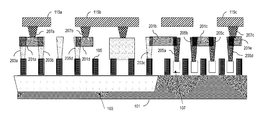
- FIG. 2A illustrates a cross sectional view of an IC device where a plurality of metal segments, for example 201 a through 201 e , of an additional metal layer, e.g., a metal-zero (M 0 ) layer, which may be implemented in middle-of-line (MOL) IC fabrication processes.
- M 0 metal-zero
- MOL middle-of-line
- the plurality of metal segments 201 a through 201 e of the M 0 layer may be utilized to provide local interconnections between two or more CB contacts 203 a through 203 d and/or two or more CA contacts 205 a through 205 d in the IC device.
- M 0 metal segment 201 a interconnects CB contacts 203 a and 203 b
- M 0 metal segment 201 b interconnects CB contact 203 c and CA contact 205 a
- M 0 metal segment 201 c interconnects CA contacts 205 b and 205 c.
- the M 0 metal segments 201 a through 201 e may provide landing pads for vias 207 a through 207 c .
- an interconnecting M 0 metal segment 201 may also provide a landing pad for a via 207 that may be connected to another metal layer.
- the M 0 metal segment 201 a provides a landing pad for via 207 a , which is connected to a segment 115 a of the M 1 layer 115 .
- M 0 metal segment 201 d is connected to CB contact 205 d and provides a landing pad for via 207 b (e.g., the via and the CB contact are not horizontally aligned), which is connected to a metal segment 115 b of the M 1 layer.
- M 0 metal segment 201 e is connected to CA contact 205 d and provides a landing pad for via 207 c , which is connected to segment 115 c of the M 1 layer, as via 207 c and CA contact 205 d are only partially aligned.
- the number of CA contacts, CB contacts, vias, and M 1 segments shown in FIG. 2A is merely exemplary.
- FIG. 2B illustrates a 3D view of some of the connections discussed in FIG. 2A where, for example, the M 0 metal segment 201 c interconnects CA contacts 205 b and 205 c , the M 0 metal segment 201 d is connected to the CB contact 205 d and provides a landing pad for the via 207 b , and the M 0 metal segment 201 e is connected to CA contact 205 d and provides a landing pad for the via 207 c.
- FIG. 2C illustrates a top view of an example layout diagram of the IC device in FIG. 2A , wherein the layout may include a plurality of contact points 209 a and 209 b .
- the layout diagram includes a contact point 209 a where a metal segment 211 a of the M 2 layer, the metal segment 115 c of the M 1 layer, the via 207 c , the CA contact 205 d , and the metal segment 201 e of the M 0 layer are interconnected.
- the via 207 c and the CA contact 205 d are misaligned, wherein the metal segment 201 e is connected to the CA contact 205 d and provides additional surface area (e.g., wider upper surface at CA contact 205 d ) for connecting with the via 207 c .
- the M 0 metal segment 201 d is connected to the CB contact 205 d, which is connected to a PC 105 .
- the metal segment 201 d also provides a complete landing pad for the via 207 b .
- metal segments of the M 2 layer e.g.
- M 2 metal segments 211 a through 211 c may be oriented perpendicular to the PCs 105 , wherein the M 2 metal segments may provide connectivity to one or more power or signal sources.
- the M 2 metal segment 211 a may provide connectivity to a negative terminal (Vss) of a power supply
- segment 211 b may provide connectivity to a bit select line
- segment 211 c may provide connectivity to a positive terminal (Vcc) of the power supply.
- Vss negative terminal
- Vcc positive terminal
- M 0 does not need an enclosure rule around contacts CA and CB because it merely extends the CA and CB area. Therefore, M 0 will not impose a rule that potentially increases chip area.
- each instance of a contact point 209 a through 209 n is associated with a PV band that includes an inner edge D 1 and an outer edge D 2 .
- the PV bands may indicate a range of minimum and maximum dimensions of an object that is to be printed onto an IC substrate. Additionally, routing/placement of neighboring contact points, for example, 209 b and 209 c , may be based on a threshold distance 215 between the neighboring contact points.
- the embodiments of the present disclosure can achieve several technical effects, including improved connections between vias and contacts without increasing chip area by utilizing metal segments of an additional metal layer as landing pads for vias and also as local interconnects between contacts in an IC device. Further, the embodiments enjoy utility in various industrial applications as, for example, microprocessors, smart phones, mobile phones, cellular handsets, set-top boxes, DVD recorders and players, automotive navigation, printers and peripherals, networking and telecom equipment, gaming systems, digital cameras, or other devices utilizing logic or high-voltage technology nodes.
- SRAM memory cells e.g., liquid crystal display (LCD) drivers, synchronous random access memories (SRAM), digital processors, etc.
- LCD liquid crystal display
- SRAM synchronous random access memories
- digital processors etc.
Abstract
Description
Claims (20)
Priority Applications (4)
| Application Number | Priority Date | Filing Date | Title |
|---|---|---|---|
| US14/540,724 US9466604B2 (en) | 2014-11-13 | 2014-11-13 | Metal segments as landing pads and local interconnects in an IC device |
| TW104122502A TWI618158B (en) | 2014-11-13 | 2015-07-13 | Metal segments as landing pads and local interconnects in an ic device |
| DE102015214848.3A DE102015214848A1 (en) | 2014-11-13 | 2015-08-04 | Metal segments as landing pads and local interconnects in an IC device |
| CN201510778463.5A CN105609466B (en) | 2014-11-13 | 2015-11-13 | Metallic section is as the regional interconnection part in then pad and IC device |
Applications Claiming Priority (1)
| Application Number | Priority Date | Filing Date | Title |
|---|---|---|---|
| US14/540,724 US9466604B2 (en) | 2014-11-13 | 2014-11-13 | Metal segments as landing pads and local interconnects in an IC device |
Publications (2)
| Publication Number | Publication Date |
|---|---|
| US20160141291A1 US20160141291A1 (en) | 2016-05-19 |
| US9466604B2 true US9466604B2 (en) | 2016-10-11 |
Family
ID=55855155
Family Applications (1)
| Application Number | Title | Priority Date | Filing Date |
|---|---|---|---|
| US14/540,724 Active 2035-01-21 US9466604B2 (en) | 2014-11-13 | 2014-11-13 | Metal segments as landing pads and local interconnects in an IC device |
Country Status (4)
| Country | Link |
|---|---|
| US (1) | US9466604B2 (en) |
| CN (1) | CN105609466B (en) |
| DE (1) | DE102015214848A1 (en) |
| TW (1) | TWI618158B (en) |
Cited By (1)
| Publication number | Priority date | Publication date | Assignee | Title |
|---|---|---|---|---|
| US10340219B2 (en) | 2017-06-08 | 2019-07-02 | Samsung Electronics Co., Ltd. | Semiconductor device having a metal via |
Families Citing this family (4)
| Publication number | Priority date | Publication date | Assignee | Title |
|---|---|---|---|---|
| US10541243B2 (en) * | 2015-11-19 | 2020-01-21 | Samsung Electronics Co., Ltd. | Semiconductor device including a gate electrode and a conductive structure |
| US10276491B2 (en) * | 2016-08-31 | 2019-04-30 | Taiwan Semiconductor Manufacturing Co., Ltd. | Interconnect structure and methods thereof |
| KR102292645B1 (en) | 2017-03-09 | 2021-08-24 | 삼성전자주식회사 | Integrated circuit device |
| EP3729495A4 (en) * | 2017-12-22 | 2021-08-11 | INTEL Corporation | Interconnect structures for integrated circuits |
Citations (2)
| Publication number | Priority date | Publication date | Assignee | Title |
|---|---|---|---|---|
| US9111907B2 (en) * | 2014-01-02 | 2015-08-18 | Globalfoundries Inc. | Silicide protection during contact metallization and resulting semiconductor structures |
| US9240413B2 (en) * | 2006-03-09 | 2016-01-19 | Tela Innovations, Inc. | Methods, structures, and designs for self-aligning local interconnects used in integrated circuits |
Family Cites Families (8)
| Publication number | Priority date | Publication date | Assignee | Title |
|---|---|---|---|---|
| CN1231959C (en) * | 2001-04-04 | 2005-12-14 | 华邦电子股份有限公司 | Method for producing metal layer virtual pattern |
| JP2007536581A (en) * | 2004-05-07 | 2007-12-13 | メンター・グラフィクス・コーポレーション | Integrated circuit layout design method using process variation band |
| KR101147261B1 (en) * | 2004-12-04 | 2012-05-18 | 엘지디스플레이 주식회사 | Thin Film Transistor Substrate of Transflective Type And Method for Fabricating The Same |
| KR100583964B1 (en) * | 2004-12-27 | 2006-05-26 | 삼성전자주식회사 | Semiconductor devices having raised cell landing pad and methods of fabricating the same |
| JP2009277719A (en) * | 2008-05-12 | 2009-11-26 | Nec Electronics Corp | Semiconductor device and method of manufacturing the same |
| CN104051529B (en) * | 2013-03-13 | 2017-07-28 | 台湾积体电路制造股份有限公司 | RF switches on high-impedance substrate |
| US9081289B2 (en) * | 2013-03-15 | 2015-07-14 | Taiwan Semiconductor Manufacturing Company, Ltd. | System and method for optimization of an imaged pattern of a semiconductor device |
| US8748245B1 (en) * | 2013-03-27 | 2014-06-10 | Io Semiconductor, Inc. | Semiconductor-on-insulator integrated circuit with interconnect below the insulator |
-
2014
- 2014-11-13 US US14/540,724 patent/US9466604B2/en active Active
-
2015
- 2015-07-13 TW TW104122502A patent/TWI618158B/en active
- 2015-08-04 DE DE102015214848.3A patent/DE102015214848A1/en not_active Ceased
- 2015-11-13 CN CN201510778463.5A patent/CN105609466B/en active Active
Patent Citations (2)
| Publication number | Priority date | Publication date | Assignee | Title |
|---|---|---|---|---|
| US9240413B2 (en) * | 2006-03-09 | 2016-01-19 | Tela Innovations, Inc. | Methods, structures, and designs for self-aligning local interconnects used in integrated circuits |
| US9111907B2 (en) * | 2014-01-02 | 2015-08-18 | Globalfoundries Inc. | Silicide protection during contact metallization and resulting semiconductor structures |
Cited By (2)
| Publication number | Priority date | Publication date | Assignee | Title |
|---|---|---|---|---|
| US10340219B2 (en) | 2017-06-08 | 2019-07-02 | Samsung Electronics Co., Ltd. | Semiconductor device having a metal via |
| US10658288B2 (en) | 2017-06-08 | 2020-05-19 | Samsung Electronics Co., Ltd. | Semiconductor device having a metal via |
Also Published As
| Publication number | Publication date |
|---|---|
| TW201618199A (en) | 2016-05-16 |
| CN105609466B (en) | 2019-09-06 |
| DE102015214848A1 (en) | 2016-05-19 |
| US20160141291A1 (en) | 2016-05-19 |
| TWI618158B (en) | 2018-03-11 |
| CN105609466A (en) | 2016-05-25 |
Similar Documents
| Publication | Publication Date | Title |
|---|---|---|
| US9466604B2 (en) | Metal segments as landing pads and local interconnects in an IC device | |
| US10103066B2 (en) | Method of utilizing trench silicide in a gate cross-couple construct | |
| US10147729B2 (en) | Structures, devices and methods for memory devices | |
| US7456447B2 (en) | Semiconductor integrated circuit device | |
| US8987128B2 (en) | Cross-coupling based design using diffusion contact structures | |
| US11238905B2 (en) | Sense amplifier layout for FinFET technology | |
| KR102201103B1 (en) | Semiconductor device | |
| US10553585B2 (en) | Semiconductor device | |
| US9105643B2 (en) | Bit cell with double patterned metal layer structures | |
| US10290639B2 (en) | VNW SRAM with trinity cross-couple PD/PU contact and method for producing the same | |
| US9431300B1 (en) | MOL architecture enabling ultra-regular cross couple | |
| US20160163644A1 (en) | Merged source/drain and gate contacts in sram bitcell | |
| US11842999B2 (en) | Semiconductor device without a break region | |
| US7122867B2 (en) | Triple well structure and method for manufacturing the same | |
| US20130093022A1 (en) | Semiconductor device | |
| US8791577B2 (en) | Bit cell with triple patterned metal layer structures | |
| US10157925B1 (en) | IC structure | |
| KR101743864B1 (en) | Vertical type cmos inverter device | |
| US10147715B2 (en) | Methods for an ESD protection circuit including trigger-voltage tunable cascode transistors | |
| US20170033061A1 (en) | Mitigating transient tsv-induced ic substrate noise and resulting devices | |
| KR20090025084A (en) | Sram device and method of fabricating the same |
Legal Events
| Date | Code | Title | Description |
|---|---|---|---|
| AS | Assignment |
Owner name: GLOBALFOUNDRIES INC., CAYMAN ISLANDS Free format text: ASSIGNMENT OF ASSIGNORS INTEREST;ASSIGNORS:WOO, YOUNGTAG;LEE, MYUNGJUN;KIM, RYAN RYOUNG-HAN;AND OTHERS;SIGNING DATES FROM 20141024 TO 20141030;REEL/FRAME:034166/0946 |
|
| FEPP | Fee payment procedure |
Free format text: PAYOR NUMBER ASSIGNED (ORIGINAL EVENT CODE: ASPN); ENTITY STATUS OF PATENT OWNER: LARGE ENTITY |
|
| STCF | Information on status: patent grant |
Free format text: PATENTED CASE |
|
| AS | Assignment |
Owner name: WILMINGTON TRUST, NATIONAL ASSOCIATION, DELAWARE Free format text: SECURITY AGREEMENT;ASSIGNOR:GLOBALFOUNDRIES INC.;REEL/FRAME:049490/0001 Effective date: 20181127 |
|
| MAFP | Maintenance fee payment |
Free format text: PAYMENT OF MAINTENANCE FEE, 4TH YEAR, LARGE ENTITY (ORIGINAL EVENT CODE: M1551); ENTITY STATUS OF PATENT OWNER: LARGE ENTITY Year of fee payment: 4 |
|
| AS | Assignment |
Owner name: GLOBALFOUNDRIES U.S. INC., CALIFORNIA Free format text: ASSIGNMENT OF ASSIGNORS INTEREST;ASSIGNOR:GLOBALFOUNDRIES INC.;REEL/FRAME:054633/0001 Effective date: 20201022 |
|
| AS | Assignment |
Owner name: GLOBALFOUNDRIES INC., CAYMAN ISLANDS Free format text: RELEASE BY SECURED PARTY;ASSIGNOR:WILMINGTON TRUST, NATIONAL ASSOCIATION;REEL/FRAME:054636/0001 Effective date: 20201117 |
|
| AS | Assignment |
Owner name: GLOBALFOUNDRIES U.S. INC., NEW YORK Free format text: RELEASE BY SECURED PARTY;ASSIGNOR:WILMINGTON TRUST, NATIONAL ASSOCIATION;REEL/FRAME:056987/0001 Effective date: 20201117 |
|
| MAFP | Maintenance fee payment |
Free format text: PAYMENT OF MAINTENANCE FEE, 8TH YEAR, LARGE ENTITY (ORIGINAL EVENT CODE: M1552); ENTITY STATUS OF PATENT OWNER: LARGE ENTITY Year of fee payment: 8 |