US9459296B2 - Electrode design for electric field measurement system - Google Patents
Electrode design for electric field measurement system Download PDFInfo
- Publication number
- US9459296B2 US9459296B2 US14/055,989 US201314055989A US9459296B2 US 9459296 B2 US9459296 B2 US 9459296B2 US 201314055989 A US201314055989 A US 201314055989A US 9459296 B2 US9459296 B2 US 9459296B2
- Authority
- US
- United States
- Prior art keywords
- electrode
- electrode arrangement
- arrangement according
- transmitting
- conductive layer
- Prior art date
- Legal status (The legal status is an assumption and is not a legal conclusion. Google has not performed a legal analysis and makes no representation as to the accuracy of the status listed.)
- Active, expires
Links
- 230000005684 electric field Effects 0.000 title claims abstract description 29
- 238000005259 measurement Methods 0.000 title description 5
- 239000000758 substrate Substances 0.000 claims abstract description 15
- 230000005540 biological transmission Effects 0.000 claims description 32
- 230000002093 peripheral effect Effects 0.000 claims description 6
- 230000003068 static effect Effects 0.000 claims 3
- 230000035945 sensitivity Effects 0.000 description 13
- 230000008878 coupling Effects 0.000 description 7
- 238000010168 coupling process Methods 0.000 description 7
- 238000005859 coupling reaction Methods 0.000 description 7
- RYGMFSIKBFXOCR-UHFFFAOYSA-N Copper Chemical compound [Cu] RYGMFSIKBFXOCR-UHFFFAOYSA-N 0.000 description 4
- 229910052802 copper Inorganic materials 0.000 description 4
- 239000010949 copper Substances 0.000 description 4
- 238000001514 detection method Methods 0.000 description 4
- 230000000694 effects Effects 0.000 description 4
- 239000012876 carrier material Substances 0.000 description 3
- 230000008859 change Effects 0.000 description 2
- 239000004020 conductor Substances 0.000 description 2
- 230000003247 decreasing effect Effects 0.000 description 2
- 238000012886 linear function Methods 0.000 description 2
- 239000002184 metal Substances 0.000 description 2
- 229910052751 metal Inorganic materials 0.000 description 2
- 239000007787 solid Substances 0.000 description 2
- 208000016057 CHAND syndrome Diseases 0.000 description 1
- 101000985487 Homo sapiens Homologous recombination OB-fold protein Proteins 0.000 description 1
- 102100028711 Homologous recombination OB-fold protein Human genes 0.000 description 1
- ATJFFYVFTNAWJD-UHFFFAOYSA-N Tin Chemical compound [Sn] ATJFFYVFTNAWJD-UHFFFAOYSA-N 0.000 description 1
- 230000008901 benefit Effects 0.000 description 1
- 238000011156 evaluation Methods 0.000 description 1
- 238000004519 manufacturing process Methods 0.000 description 1
- 238000000034 method Methods 0.000 description 1
- 230000008569 process Effects 0.000 description 1
- 230000009467 reduction Effects 0.000 description 1
- 239000000523 sample Substances 0.000 description 1
- XOLBLPGZBRYERU-UHFFFAOYSA-N tin dioxide Chemical compound O=[Sn]=O XOLBLPGZBRYERU-UHFFFAOYSA-N 0.000 description 1
- 229910001887 tin oxide Inorganic materials 0.000 description 1
Images


Classifications
-
- H—ELECTRICITY
- H03—ELECTRONIC CIRCUITRY
- H03K—PULSE TECHNIQUE
- H03K17/00—Electronic switching or gating, i.e. not by contact-making and –breaking
- H03K17/94—Electronic switching or gating, i.e. not by contact-making and –breaking characterised by the way in which the control signals are generated
- H03K17/96—Touch switches
- H03K17/962—Capacitive touch switches
-
- G—PHYSICS
- G01—MEASURING; TESTING
- G01R—MEASURING ELECTRIC VARIABLES; MEASURING MAGNETIC VARIABLES
- G01R27/00—Arrangements for measuring resistance, reactance, impedance, or electric characteristics derived therefrom
- G01R27/02—Measuring real or complex resistance, reactance, impedance, or other two-pole characteristics derived therefrom, e.g. time constant
- G01R27/26—Measuring inductance or capacitance; Measuring quality factor, e.g. by using the resonance method; Measuring loss factor; Measuring dielectric constants ; Measuring impedance or related variables
- G01R27/2605—Measuring capacitance
-
- H—ELECTRICITY
- H03—ELECTRONIC CIRCUITRY
- H03K—PULSE TECHNIQUE
- H03K17/00—Electronic switching or gating, i.e. not by contact-making and –breaking
- H03K17/94—Electronic switching or gating, i.e. not by contact-making and –breaking characterised by the way in which the control signals are generated
- H03K17/96—Touch switches
- H03K2017/9602—Touch switches characterised by the type or shape of the sensing electrodes
-
- H—ELECTRICITY
- H03—ELECTRONIC CIRCUITRY
- H03K—PULSE TECHNIQUE
- H03K2217/00—Indexing scheme related to electronic switching or gating, i.e. not by contact-making or -breaking covered by H03K17/00
- H03K2217/94—Indexing scheme related to electronic switching or gating, i.e. not by contact-making or -breaking covered by H03K17/00 characterised by the way in which the control signal is generated
- H03K2217/96—Touch switches
- H03K2217/9607—Capacitive touch switches
- H03K2217/960755—Constructional details of capacitive touch and proximity switches
Definitions
- the present disclosure relates to electrodes, in particular the design of an electrode for use in an electric field measurement system.
- Human device interfaces in particular for mobile devices often use sensors arrangements for detecting an user input that do not necessarily require any movable parts. Examples are touch screens and capacitive switches that are required to be touched to be activated.
- Such sensor systems comprise electrodes that are arranged on the device wherein if a user touches them or gets into very close proximity a change in capacitance can be measured to trigger an event. These electrodes are often formed by small metal plates, etched areas on a circuit board, or areas in a metal layer such as a transparent TIN oxide layer for use in displays.
- Similar electrodes can also be used for electric field measurement.
- This type of sensor device allows detection of an object without touching and at far greater distances from the device as conventional capacitive sensor systems.
- an electrode is used as a transmitter to project an electric field outside or in front of a respective device.
- the field may be generated by a 30-200 kHz, in particular a 70-140 kHz or a 40-115 kHz, signal and thus is quasi-static in the near field.
- the same electrode or a separate receiver electrode can be used to detect these changes. If a plurality of such electrodes are used in a sensing system, multi-dimensional gesture detection becomes possible which allows operation of the device without touching it.
- the sensors often need to be shielded or arranged in specific order and then may be coupled to a front end integrated circuit device for evaluation of incoming signals.
- Sensitivity of electrodes used in a system that generates a quasi-static electric field and sense disturbances in that field when an object enters the field is often low, in particular in a system that uses solid electrodes. Hence, there exists a need for improved electrodes and electrode arrangements.
- an electrode arrangement for an electric field sensor device generating a quasi-static electric field with at least one transmitting electrode and at least one receiving electrode comprising a nonconductive substrate having a first conductive layer and a second conductive layer, a first electrode arranged within the first conductive layer, wherein the first electrode is a receiving electrode of the electric field sensor device, and a second electrode arranged within the second conductive layer, wherein the second electrode is a transmitting electrode of the electric field sensor device wherein the second electrode covers a larger area than the first electrode and wherein the first and/or second electrode is textured to reduce the capacitance between the first and second electrode.
- only the second electrode can be textured such that it comprises at least one cut-out area having a similar form of the first electrode and being located under the first electrode such that the first electrode covers the cut-out area.
- the entire area of the second electrode can be textured by a hash or hatch texture.
- the texture can be formed by a plurality of conductive lines.
- the hash or hatch texture can be homogenous.
- the hash or hatch texture can be formed by a plurality of conductive lines forming a mesh.
- the mesh can be formed by a first set of parallel arranged conductive lines and a second set of parallel arranged conductive lines.
- the first set of parallel arranged conductive lines may cross said second set of parallel arranged conductive lines at an angle of 90 degrees.
- the mesh may comprise a peripheral conductive line enclosing the mesh.
- the second electrode can be textured to provide a plurality of grooves.
- the grooves can be arranged in parallel at predefined distances.
- only the first electrode is textured.
- the electrode arrangement may further comprise a plurality of first electrodes arranged above said second electrode and a plurality of feeding lines for electrical connection to said second electrodes.
- At least one set of four first electrodes can be arranged to define a rectangular area.
- the electrode arrangement may further comprise a center electrode within the rectangular area defined by the four electrodes.
- the second electrode can be textured as a mesh electrode and only covers the rectangular area defined by the at least one set of four first electrodes.
- the feeding lines may have a width of about 0.15 mm.
- the first conductive layer can be a top layer of a printed circuit board.
- the second conductive layer can be a bottom layer of a printed circuit board.
- the first conductive layer can be a transparent conductive top layer on a transparent isolating carrier material.
- the second conductive layer can be a bottom layer on the transparent isolating carrier material.
- the feeding lines and said second electrode can be arranged within an inner layer of a multi-layer printed circuit board.
- a bottom layer of the multi-layer printed circuit board can be connected to ground.
- the electrode arrangement may further comprise a front end analog device coupled with said receiving electrodes through said feeding lines.
- the front end analog device may comprise a voltage divider for attenuating a signal received through said feeding lines.
- the voltage divider may comprise a frequency compensation.
- the electrode arrangement may comprise a plurality of second electrodes electrically insulated from each other each forming a partial transmission electrode.
- each transmission electrode can be formed by a rectangular electrode section.
- FIG. 1 shows a solid transmission (Tx) electrode on the bottom layer and receiving (Rx) electrode on the top layer of a dielectric substrate
- FIG. 2 shows a similar arrangement with a cutout Tx electrode area underneath an Rx electrode according to various embodiments
- FIG. 3 shows a textured Tx electrode according to an embodiment
- FIG. 4 shows a textured Tx electrode according to another embodiment
- FIG. 5 shows a textured Tx electrode with Tx cutout underneath the Rx electrode according to an embodiment
- FIG. 6 shows a standard electrode equivalent circuit
- FIG. 7 shows an extended electrode equivalent circuit according to various embodiments
- FIG. 8 shows a typical arrangement of transmitting and receiving electrodes in an electric field gesture detection system
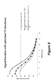
- FIG. 9 shows signal deviation with optimized Tx structures according to various embodiments.
- FIG. 10 shows another example of a sensor system according to various embodiments.
- FIG. 11 shows a sectional view through a printed circuit board, for example, the circuit board shown in FIG. 10 .
- FIG. 12 shows a top view of yet another embodiment of an electrode arrangement.
- electrode design in particular for use with an integrated front end device can be improved enabling significant higher sensitivity to the object to be tracked, for example a user's hand.
- FIG. 1 shows a conventional layout 100 of a transmission electrode 120 and a single reception electrode 110 for a quasi-static electric field sensor system. More or less transmitting and receiving electrodes may be used but for clarity purposes only one transmitting electrode is shown in FIG. 1 . Also, in this embodiment only a single reception electrode 110 arranged on a top layer of a dielectric carrier substrate 130 is shown. However, a plurality of separate reception electrodes 110 may be arranged on the top layer of dielectric carrier substrate 130 . The transmission electrode 120 is arranged on the bottom layer of dielectric carrier substrate 130 . This arrangement causes a capacitive link between the transmission and reception electrode.
- the transmission electrode will be fed with an alternating signal, for example a square wave signal generated by a microcontroller having a frequency of about 30-200 kHz, in particular about 70-140 kHz or 40-115 kHz. Other suitable frequency ranges may apply.
- an alternating signal for example a square wave signal generated by a microcontroller having a frequency of about 30-200 kHz, in particular about 70-140 kHz or 40-115 kHz. Other suitable frequency ranges may apply.
- This generates a quasi-static electric field above and below the transmission electrode plane. In most applications only the field generated away from the transmission electrode 120 in direction of the receiving electrode 110 is of interest.
- a signal at the receiving electrode will change due to capacitive influences caused by the object. Such disturbances vary with the distance of the object to the electrodes.
- a front end circuit can detect such signal changes and further evaluate or process these signals.
- dS ⁇ V Tx ⁇ a[C Hand /( C RxTx +C L +2( C N +C RxG +a ⁇ C Buf )+( C N +C RxG +a ⁇ C Buf ) 2 /( C RxTx +C L ))]
- dS is approximately a linear function of the hand capacitance C Hand .
- C RxTx is the capacitance between the transmission and reception electrode.
- C Buf is the input capacitance of the input buffer of the front-end integrated circuit device.
- C L is the capacitance created between the Rx feeding line and the Tx electrode.
- C N is the noise coupling capacitance.
- C RxG is the capacitance between Rx electrode and ground.
- Parameter ‘a’ is an attenuation factor determined by the voltage divider used in the input circuit.
- a first solution for factor (a) can be achieved by maximizing the distance of the Rx feeding lines to the Tx electrode and its feeding lines. Nevertheless, this is a tradeoff between shielding the Rx feeding line from hand influences which is recommended. According to various embodiments, the above equation shows that it is better to shield the Rx feeding line with a Tx signal instead of ground. Ground shielding would increase C RxG which has a more negative impact on the system sensitivity than C L . It is always good to make the Rx feeding lines as thin as possible. This minimizes both the feeding line capacitance to Tx and to ground as well as the influence of the hand to the feeding line.
- a second solution for factor (a) can be achieved when using an active guard/shield around the Rx feeding line, where the guard/shield is driven actively by the received and buffered input signal.
- this guard would be a coax cable which completely encloses the feeding line.
- Other less optimum designs are shielding from the top and/or from both sides.
- a solution for factor (b) can be achieved in general by maximizing the distance between the Rx-Tx electrode stack up and ground. Since ground parts typically cover large areas in an integrated front-end system e-field stray effects dominate typically C RxG and it often doesn't make sense to increase the Rx electrode distance to ground to more than a few millimeters.
- a first solution for factor (c) can be achieved by increasing the distance between the Rx and the Tx electrode.
- C RxTx dominates the other capacitances in above equation.
- the capacitance between the Rx and the Tx electrode can be decreased while the useful capacitance C Hand between Rx and the hand kept in the same order of magnitude. Since in a typical integrated front-end design a smaller Rx receive electrode 110 is placed on top of the larger transmitting Tx electrode 120 the Rx-Tx capacitance can assumed to be the plate capacitance of the face to face areas of the Rx and Tx superimposed with the capacitance created from the stray e-field from the Rx electrode 110 to the much larger Tx electrode 120 as shown in FIG. 1 .
- the target object influences in this model only the stray field but not the plate capacitance between the face-to-face areas of Rx and Tx.
- the plate capacitance versus the Rx-Tx stray capacitance is minimized and by this the influence of the hand to the stray field is maximized.
- This can be achieved by cutout 240 (leave open) of the Tx electrode 210 underneath the Rx electrode 220 as shown, e.g., with electrode arrangement 200 in FIG. 2 .
- a substrate 230 such as a printed circuit board or any other suitable carrier provides on one side for the transmitting electrode 220 and on the other side for the receiving electrode 210 .
- the cut-out area 240 does not need to exactly match the size of the Rx electrode 220 . As will be shown below with FIG. 10 , the cut-out area can also be larger, for example extend to cover an entire exterior area when four Rx electrodes are arranged to define a rectangular sensing area.
- the Rx electrode 210 is typically shielded by the Tx electrode 220 from the (device) ground. Therefore C RxG is typically smaller than the C RxTx capacitance. C N and C Buf are very low anyhow as will be discussed below in more detail.
- a proposed solution of an arrangement 300 as shown in FIG. 3 is to hash/texture the Tx electrode surface 310 in order to reduce the (plate) capacitance between Rx and Tx.
- FIGS. 3 and 4 show different embodiments 300 and 400 wherein the transmitting electrode is differently textured in each case. Thus, different structures are possible.
- a textured electrode may have different shapes.
- a hash or hatch pattern may be used to texture an electrode.
- the terms “hash pattern” and “hatch pattern” are considered to be equivalent terms in this disclosure.
- the main aspect of texturing an electrode is to reduce the effective electrode area while not changing the size of the electrode.
- FIG. 10 shows examples of two textured electrodes 1050 and 1060 and will be discussed in more detail below.
- a grid of crossing connection lines may be used to form an electrode area as shown in FIG. 10 .
- a plurality of parallel conductive stripes or conductive lines may be used as shown in FIG. 4 .
- the lines may be all interconnected on one or both ends of the respective structure. In the embodiment shown in FIG.
- the additional cut-out 520 might separate the various conducting lines if a striped pattern is chosen for the transmitting electrode 510 .
- any electrically separated sections may be connected by additional feed lines or connected at the peripheral edge if possible.
- a textured electrode for example when formed by a copper layer of a printed circuit board or a transparent TIN layer, for example in a display, basically removes a certain amount of copper or conductive material and thus reduces the capacitive coupling of such an electrode while the over-all size remains the same.
- a texture can be simply formed by a plurality of conductive lines. In one embodiment, these lines may cross each other, in other embodiments no crossing takes place and the lines are connected with each other in a peripheral area.
- the receiving electrodes may also be textured electrodes.
- only the transmitting electrodes are textured, in some embodiments, both, the receiving and the transmitting electrodes may be textured, and in some embodiments only the receiving electrodes are textured.
- FIG. 5 shows an embodiment 500 in which a textured transmission electrode 510 according to the embodiments of FIG. 3 or 4 further provides for a cut-out area 520 underneath the receiving electrode according to the embodiment of FIG. 2 .
- the cut-out area is used to further reduce the capacitive coupling and therefore does not need to match the area of the respective receiving electrode under which it is arranged.
- a hash or hatch pattern of different density compared to the texture of the remaining transmission electrode 510 can be used to balance the capacitances (C RxTx +C L ) and (C N +C RxG a ⁇ C Buf ).
- an area within the transmission electrode Tx below a receiving electrode may have, for example, a texture with thinner lines or less lines thereby reducing the capacitance between Tx and Rx electrodes.
- FIG. 8 shows a three-dimensional view of yet another example of an electrode arrangement 800 on a substrate 840 .
- two Rx electrodes 810 , 820 are shown which are elongated strips of conductive material, such as copper, arranged along or adjacent the border lines of the substrate.
- the Tx electrode 830 may be textured according to the embodiments shown in FIGS. 3 and 4 and arranged on the backside of substrate 840 .
- FIG. 9 shows signal deviation with optimized Tx structures according to various embodiments. As can be seen, the reduction of capacitance between the Tx and Rx electrodes yields to highly improved deviations and therefore better signal detection.
- the bottom curve shows the signal deviation of a conventional arrangement.
- the middle curve shows results for an arrangement with a hashed Tx electrode, for example according to FIG. 3 .
- the top curve shows the effect of a combination of hashing and cut-out in the Tx electrode, for example according to FIG. 5 .
- FIG. 10 shows a top view of yet another embodiment of an electrode arrangement 1000 .
- the a first set of outer receiving electrodes 1010 b, c, d are arranged on opposites sides on top of a printed circuit board, which may be designed to also comprise the entire front end circuitry, for example on the periphery of the board.
- a second set of receiving electrodes 1040 , a, b, c, d may be arranged inside the area framed by the outer electrode set 1010 , a, b, c, d .
- the second set of receiving electrodes 1040 , a, b, c, d can be spaced apart from the first set of electrodes 1010 , a, b, c, d as shown in FIG.
- the center area can be filled with a specially designed center electrode 1060 which can be used to enhance the resolution of the z-coordinate perpendicular to the electrode area in close proximity.
- the center electrode 1060 can be used as a touch electrode.
- the entire sensor arrangement may comprise an outer shielding ring (not shown in FIG. 10 ).
- the center electrode 1060 is formed by a grid or mesh formed by conductive paths. All electrodes 1010 , 1040 and 1060 on the top of the substrate can be formed by the top copper layer of the printed circuit board according to an embodiment.
- the printed circuit board may be a multi-layer board and feeding lines 1020 may connect to each electrode 1010 , 1030 , 1060 on the top layer through respective vias as known in the art of printed circuit board manufacturing.
- an area 1030 may be used as a general connection area from which a plurality of feed lines 1020 connect to the respective electrodes 101 , 1040 and 1060 .
- the inner second set of electrodes 1040 may be omitted and a respective larger center electrode 1060 may be formed accordingly.
- the number and arrangement of Rx electrodes 1010 , 1040 is of course not limited to the arrangement shown in FIG. 10 . Other configurations may apply.
- the transmitting electrode 1050 can be formed on the backside of the printed circuit board or within an inner layer of a multi-layer printed circuit board and may be designed to have a grid pattern as shown in FIG. 10 .
- a plurality of square areas may be etched away to form the grid according to one embodiment.
- the grid is formed by a plurality of crossing vertical and horizontal conductive lines.
- transmitting electrode 1050 may consist of multiple section or in other words may be divided by the feeding lines 1020 . Each section may have a peripheral conductive line that encompasses the entire section.
- center electrode 1060 shows such a peripheral conductive line that encompasses the entire center electrode 1060 .
- the mesh within the center electrode 1060 is not only wider spaced than the mesh of the transmitting electrode 1050 but also arranged at an angle with respect to the mesh formed by the transmitting electrode 1050 .
- Other patterns are possible to form such a textured structures.
- a structure similar to that used for the center electrode 1060 may be used.
- the center electrode 1060 may also be used as a shielding electrode which may receive a phase shifted signal derived from the main transmission signal fed to the transmitting electrode 1050 .
- the transmitting electrode 1050 does not overlap with the outer receiving electrodes 1010 , a, b, c, d .
- the capacitive coupling between these receiving electrodes 1010 , a, b, c, d and the transmitting electrode 1050 is further reduced.
- the cut-out area covers the entire external periphery defined by the four electrodes 1010 a, b, c, d .
- a designed as proposed in FIG. 2 could also be used.
- the feeding connection lines could be formed within an inner layer of the printed circuit board.
- the transmission electrode can also be formed within an inner layer according to an embodiment.
- the transmission electrode and the feeding lines can be formed in an inner layer and the receiving electrodes can be formed in a top layer whereas a bottom layer may be used as a ground layer shielding both Tx and Rx electrodes.
- Multilayer printed circuit boards may be designed in a similar manner wherein additional layers in the electrode area may not be used, or only used for the feed lines. FIG.
- FIG. 11 shows an exemplary four layer printed circuit board with the Rx electrodes arranged within the top or first layer and the Tx electrode and feeding lines arranged within the third layer, wherein the fourth or bottom layer is used as a ground shielding layer.
- the second layer as shown in FIG. 11 may be omitted entirely.
- a simple two-sided circuit board may be used and the feed lines 1020 can be arranged on the bottom side. Any section separated by a feed line 1020 may be separately connected, for example in the area 1030 .
- FIG. 12 shows a top view of yet another embodiment in which multiple transmission electrodes Tx 1 , Tx 2 . . . TxM are arranged underneath the receiving electrodes Rx 1 , Rx 2 . . . RxN.
- Each transmission electrodes Tx 1 , Tx 2 . . . TxM is electrically insulated from each other and, thus, the respective transmission electrodes Tx 1 , Tx 2 . . . TxM can be controlled separately or one or more or even all transmission electrodes Tx 1 , Tx 2 . . . TxM can be fed with the same transmission signal.
- a single transmission electrode Tx a plurality of transmission electrodes Tx 1 , Tx 2 . . .
- TxM may be arranged in parallel, for example, the transmission electrodes may be rectangular strips as shown in FIG. 12 . However, other electrode forms may be used and the transmission electrodes may be arranged to form a homogenous texture or any other texture.
- Each transmission electrode Tx 1 , Tx 2 . . . TxM may have the same shape as shown in FIG. 11 . However, other embodiments may be used in which the transmission electrodes have different shapes and/or sizes. Such an arrangement may allow for a proximity and touch sensor system with improved spatial resolution.
- the transmission electrodes Tx 1 , Tx 2 . . . TxM and/or receiving electrodes Rx 1 , Rx 2 . . . RxN may also use a hash or hatch pattern as discussed above in particular to reduce the capacitance between the respective portions of the transmission and receiving electrodes that are most responsible for the capacitance between transmission and receiving electrodes.
- FIG. 6 shows a standard electrode equivalent circuit
- V TxD the analog front end device voltage
- V RxBuf the analog front end Rx buffer input voltage
- V h the auxiliary voltage to derive V RxBuf
- V N the external noise voltage to be injected to the receiving electrode e Rx
- FIG. 7 shows an extended electrode equivalent circuit according to various embodiments, with
- V TxD the analog front end device voltage
- V RxBuf the analog front end Rx buffer input voltage
- V h the auxiliary voltage to derive V RxBuf
- V N the external noise voltage to be injected to the receiving electrode e Rx
- An external capacitance C D and resistor R D can be used to reduce the input voltage V RxBuf to a defined level that under high noise conditions the input buffer is not overloaded.
- the resistor R D is used to realize a frequency compensated voltage divider.
- Tx output voltage of the chip It may not be desirable to reduce the Tx output voltage of the chip.
- a best signal-to-noise ratios may be achieved with a maximum Tx signal, as shown below.
- an external Tx signal boost amplifier can be considered when required.
- the buffer input resistance has a much lower effect than the buffer input capacitance in the relevant frequency range of 30-200 kHz and for now it is assumed that
- V RxBuf ⁇ [ V Tx 1 + C N + C RxG + ⁇ ⁇ C Buf + C H C RxTx + C L + V N 1 + C RxTx + C L + C RxG + ⁇ ⁇ C Buf + C H C N ] ( 4 ) 4. Receiver Signal Sensitivity
- Equation (7) shows it is better to shield the Rx feeding line with a Tx signal instead of ground. Ground shielding would increase C RxG which has a more negative impact on the system sensitivity than C L (see also equation (7)). It may be always a good idea to make the Rx feeding lines as thin as possible. This minimizes both the feeding line capacitance to Tx and to ground as well as the influence of the hand to the feeding line.
- (b) can be achieved in general by maximizing the distance between the Rx-Tx electrode stack up and ground. Since ground parts typically cover large areas in a an analog front end system, e-field stray effects dominate typically C RxG and it often doesn't make sense to increase the Rx electrode distance to ground to more than a few millimeters.
- (c) can be achieved by increasing the distance between the Rx and the Tx electrode.
- C RxTx dominates the other capacitances.
- C Hand is small compared to the Tx-Rx electrode capacitance
- S D is given typically in LSBs (lowest significant bit) of a 16-bit integer value.
- the SNR is independent from the attenuation factor a and the hand.
- the optional voltage divider is set to an attenuation factor a avoiding overloading the input channel under all noise conditions.
- no voltage divider is used and optimum capacitive values are chosen.
- the transmit voltage level is set to 2Vpp in order to avoid an overload of the input buffer under all noise conditions:
- V Tx 2V pp
- the buffer signal without noise is with first term of equation (4)
- V RxBuf V Tx ⁇ 1 1 + C N + C RxG + C Buf + C H C RxTx + C L
- the SNR becomes
- an 2:3 voltage divider is used and same optimum capacitive values as above are chosen.
- the transmit voltage level is set to the maximum output level of the analog front end device.
- V Tx 3V pp
- V RxBuf ⁇ ⁇ V Tx 1 + C N + C RxG + ⁇ ⁇ C Buf + C H C RxTx + C L
- ⁇ ⁇ ⁇ S 3 ⁇ V pp ⁇ ⁇ [ 0.5 ⁇ ⁇ pF 15 ⁇ ⁇ pF + 5 ⁇ ⁇ pF + 2 ⁇ ( 1 ⁇ ⁇ pF + 7 ⁇ ⁇ pF + 3.3 ⁇ ⁇ pF ) + ( 1 ⁇ ⁇ pF + 7 ⁇ ⁇ pF + 3.3 ⁇ ⁇ pF ) 2 / ( 15 ⁇ ⁇ pF + 5 ⁇ ⁇ pF ) ]
- the SNR becomes
- the second example demonstrates that with about the same signal levels at the receiver input, the SNR is improved by about 3.5 dB as expected.
- the signal deviation produced by the hand is 11% higher than in example 1.
- V Tx 2V pp
- V N 3 V rms 32 8.5 V pp
- V RxBuf V Tx ⁇ 1 1 + C N + C RxG + C Buf + C H C RxTx + C L
- the SNR becomes
- the received signal level at the Rx input buffer is similar to the previous examples.
- the SNR is the same compared to the second example where a higher Tx transmit voltage was used.
- the gain of the boost amplifier should typically not exceed more than 6, to allow a voltage divider capacitance above 1 pF.
Landscapes
- Physics & Mathematics (AREA)
- General Physics & Mathematics (AREA)
- Switches That Are Operated By Magnetic Or Electric Fields (AREA)
- Measurement Of Length, Angles, Or The Like Using Electric Or Magnetic Means (AREA)
- Measurement And Recording Of Electrical Phenomena And Electrical Characteristics Of The Living Body (AREA)
- Position Input By Displaying (AREA)
- Electronic Switches (AREA)
Abstract
Description
dS≈V Tx ·a[C Hand/(C RxTx +C L+2(C N +C RxG +a·C Buf)+(C N +C RxG +a·C Buf)2/(C RxTx +C L))]
where dS is approximately a linear function of the hand capacitance CHand. CRxTx is the capacitance between the transmission and reception electrode. CBuf is the input capacitance of the input buffer of the front-end integrated circuit device. CL is the capacitance created between the Rx feeding line and the Tx electrode. CN is the noise coupling capacitance. CRxG is the capacitance between Rx electrode and ground. Parameter ‘a’ is an attenuation factor determined by the voltage divider used in the input circuit.
R D ·C D =R Buf ·C Buf
4. Receiver Signal Sensitivity
In a typical analog front end setup it can be assumed that the hand capacitance CHand is much smaller than the Rx-Tx electrode capacitance C and equation (6) becomes
Claims (23)
Priority Applications (9)
| Application Number | Priority Date | Filing Date | Title |
|---|---|---|---|
| US14/055,989 US9459296B2 (en) | 2012-10-19 | 2013-10-17 | Electrode design for electric field measurement system |
| PCT/EP2013/071905 WO2014060603A1 (en) | 2012-10-19 | 2013-10-18 | Electrode design for electric field measurement system |
| TW102137797A TWI598797B (en) | 2012-10-19 | 2013-10-18 | Electrode design for electric field measurement system |
| KR1020157012176A KR102027908B1 (en) | 2012-10-19 | 2013-10-18 | Electrode design for electric field measurement system |
| EP13779818.7A EP2909939B1 (en) | 2012-10-19 | 2013-10-18 | Electrode design for electric field measurement system |
| JP2015537283A JP6291500B2 (en) | 2012-10-19 | 2013-10-18 | Electrode design for electric field measurement system |
| CN201380063805.4A CN104838591B (en) | 2012-10-19 | 2013-10-18 | Electrode design for electric field measurement system |
| US15/209,321 US10873330B2 (en) | 2012-10-19 | 2016-07-13 | Electrode design for electric field measurement system |
| JP2018021632A JP6529200B2 (en) | 2012-10-19 | 2018-02-09 | Electrode design for electric field measurement system |
Applications Claiming Priority (2)
| Application Number | Priority Date | Filing Date | Title |
|---|---|---|---|
| US201261715966P | 2012-10-19 | 2012-10-19 | |
| US14/055,989 US9459296B2 (en) | 2012-10-19 | 2013-10-17 | Electrode design for electric field measurement system |
Related Child Applications (1)
| Application Number | Title | Priority Date | Filing Date |
|---|---|---|---|
| US15/209,321 Continuation US10873330B2 (en) | 2012-10-19 | 2016-07-13 | Electrode design for electric field measurement system |
Publications (2)
| Publication Number | Publication Date |
|---|---|
| US20140111222A1 US20140111222A1 (en) | 2014-04-24 |
| US9459296B2 true US9459296B2 (en) | 2016-10-04 |
Family
ID=50484792
Family Applications (2)
| Application Number | Title | Priority Date | Filing Date |
|---|---|---|---|
| US14/055,989 Active 2033-12-21 US9459296B2 (en) | 2012-10-19 | 2013-10-17 | Electrode design for electric field measurement system |
| US15/209,321 Active 2034-11-11 US10873330B2 (en) | 2012-10-19 | 2016-07-13 | Electrode design for electric field measurement system |
Family Applications After (1)
| Application Number | Title | Priority Date | Filing Date |
|---|---|---|---|
| US15/209,321 Active 2034-11-11 US10873330B2 (en) | 2012-10-19 | 2016-07-13 | Electrode design for electric field measurement system |
Country Status (7)
| Country | Link |
|---|---|
| US (2) | US9459296B2 (en) |
| EP (1) | EP2909939B1 (en) |
| JP (2) | JP6291500B2 (en) |
| KR (1) | KR102027908B1 (en) |
| CN (1) | CN104838591B (en) |
| TW (1) | TWI598797B (en) |
| WO (1) | WO2014060603A1 (en) |
Cited By (1)
| Publication number | Priority date | Publication date | Assignee | Title |
|---|---|---|---|---|
| US20160313851A1 (en) * | 2015-04-22 | 2016-10-27 | Microchip Technology Incorporated | Capacitive Sensor System With Multiple Transmit Electrodes |
Families Citing this family (11)
| Publication number | Priority date | Publication date | Assignee | Title |
|---|---|---|---|---|
| DE102009057933B3 (en) * | 2009-12-11 | 2011-02-24 | Ident Technology Ag | Sensor device for detecting approach and touch of e.g. hand held device by hand, has electrode structure including transmission, compensation and receiving electrodes, where electrical field is received in receiving electrode |
| US9459296B2 (en) | 2012-10-19 | 2016-10-04 | Microchip Technology Germany Gmbh Ii & Co. Kg | Electrode design for electric field measurement system |
| FR3008809B1 (en) * | 2013-07-18 | 2017-07-07 | Fogale Nanotech | CUSTOM ACCESSORY DEVICE FOR AN ELECTRONIC AND / OR COMPUTER APPARATUS, AND APPARATUS EQUIPPED WITH SUCH AN ACCESSORY DEVICE |
| FR3013472B1 (en) | 2013-11-19 | 2016-07-08 | Fogale Nanotech | COVERING ACCESSORY DEVICE FOR AN ELECTRONIC AND / OR COMPUTER PORTABLE APPARATUS, AND APPARATUS EQUIPPED WITH SUCH AN ACCESSORY DEVICE |
| CN104267266B (en) * | 2014-09-23 | 2017-02-01 | 清华大学 | Electric field measurement sensing device based on piezoelectric buckling effect |
| DE102015223534B4 (en) | 2015-11-27 | 2019-05-23 | Siemens Healthcare Gmbh | Circuit arrangement for reducing the maximum electric field strength, high-voltage generation unit with such a circuit arrangement and X-ray generator with such a high-voltage generation unit |
| JP6815105B2 (en) * | 2016-06-28 | 2021-01-20 | セーレン株式会社 | Electric field sensor |
| KR102635976B1 (en) | 2016-12-30 | 2024-02-13 | 에스엘 주식회사 | The Apparatus For Recognizing Gesture |
| WO2020046207A1 (en) * | 2018-08-31 | 2020-03-05 | National University Of Singapore | Method and system for integrity testing of blister packages |
| CN110596472A (en) * | 2019-09-29 | 2019-12-20 | 清华大学 | Dielectric polarization capacitance type electrostatic field measuring method and system |
| WO2021198404A1 (en) * | 2020-04-03 | 2021-10-07 | Continental Teves Ag & Co. Ohg | Estimation method of discrete digital signals in noisy overloaded wireless communication systems with csi errors |
Citations (14)
| Publication number | Priority date | Publication date | Assignee | Title |
|---|---|---|---|---|
| GB2435998A (en) | 2005-09-20 | 2007-09-12 | Harald Philipp | Capacitive touch sensor for preventing walk by interference |
| US20080122798A1 (en) * | 2006-10-13 | 2008-05-29 | Atsushi Koshiyama | Information display apparatus with proximity detection performance and information display method using the same |
| US20100292945A1 (en) * | 2009-05-13 | 2010-11-18 | Joseph Kurth Reynolds | Capacitive sensor device |
| US20110053357A1 (en) * | 2009-08-25 | 2011-03-03 | Semiconductor Energy Laboratory Co., Ltd. | Plasma cvd apparatus, method for forming microcrystalline semiconductor film and method for manufacturing semiconductor device |
| US20110156930A1 (en) | 2009-12-24 | 2011-06-30 | Orise Technology Co., Ltd. | Capacitive Touch Panel with High Touching Sensitivity |
| WO2011128116A2 (en) * | 2010-04-16 | 2011-10-20 | Ident Technology Ag | Tft display, oled-interface, and method for detecting the spatial position of rims in a spatial region disposed upstream of a display |
| US20120044198A1 (en) | 2010-06-30 | 2012-02-23 | Cypress Semiconductor Corporation | Self shielding capacitance sensing panel |
| US8243027B2 (en) * | 2006-06-09 | 2012-08-14 | Apple Inc. | Touch screen liquid crystal display |
| US20120229417A1 (en) * | 2011-03-11 | 2012-09-13 | Cypress Semiconductor Corporation | Two Prong Capacitive Sensor Pattern |
| US20120262391A1 (en) | 2011-04-15 | 2012-10-18 | Panasonic Corporation | Touch screen device and plasma display apparatus having the same |
| US8803823B2 (en) * | 2010-02-04 | 2014-08-12 | Shenzhen Huiding Technology Co., Ltd. | Capacitive touch sensor, touch detection device and touch terminal |
| US20140240285A1 (en) * | 2013-02-18 | 2014-08-28 | Bernard J. Hermes | Detecting Presence of an Object in the Vicinity of a Touch Interface of a Device |
| US20140267155A1 (en) * | 2013-03-15 | 2014-09-18 | Microchip Technology Incorporated | Matrix Electrode Design for Three-Dimensional E-Field Sensor |
| US20140267137A1 (en) * | 2013-03-14 | 2014-09-18 | Synaptics Incorporated | Proximity sensing using driven ground plane |
Family Cites Families (15)
| Publication number | Priority date | Publication date | Assignee | Title |
|---|---|---|---|---|
| US5315232A (en) * | 1991-01-03 | 1994-05-24 | Stewart Michael F | Electric field measuring system |
| US5691635A (en) * | 1996-01-29 | 1997-11-25 | Fluke Corporation | Probe identification system for a measurement instrument |
| JPH09274093A (en) | 1996-04-08 | 1997-10-21 | Hitachi Ltd | Boiling water reactor |
| TW200901014A (en) * | 2007-06-28 | 2009-01-01 | Sense Pad Tech Co Ltd | Touch panel device |
| US20090107737A1 (en) * | 2007-10-28 | 2009-04-30 | Joesph K Reynolds | Multiple-sensor-electrode capacitive button |
| JP5540520B2 (en) | 2009-02-16 | 2014-07-02 | ソニー株式会社 | Capacitive element, capacitive element design method, and integrated circuit device including the capacitive element |
| US8810249B2 (en) * | 2009-03-20 | 2014-08-19 | Thomas G. Cehelnik | E-field sensor arrays for interactive gaming, computer interfaces, machine vision, medical imaging, and geological exploration CIP |
| US8599150B2 (en) | 2009-10-29 | 2013-12-03 | Atmel Corporation | Touchscreen electrode configuration |
| KR101769889B1 (en) * | 2010-02-10 | 2017-08-21 | 마이크로칩 테크놀로지 저머니 게엠베하 | System and method for the generation of a signal correlated with a manual input operation |
| DE102010031034A1 (en) * | 2010-07-07 | 2012-01-12 | Robert Bosch Gmbh | Detecting a dielectric object |
| JP2012068724A (en) * | 2010-09-21 | 2012-04-05 | Shin Etsu Polymer Co Ltd | Input device |
| US9337833B2 (en) * | 2011-11-14 | 2016-05-10 | Atmel Corporation | Driven shield for shaping an electric field of a touch sensor |
| US20130181911A1 (en) * | 2012-01-17 | 2013-07-18 | Esat Yilmaz | On-Display-Sensor Stack |
| US9459296B2 (en) | 2012-10-19 | 2016-10-04 | Microchip Technology Germany Gmbh Ii & Co. Kg | Electrode design for electric field measurement system |
| US9946410B2 (en) * | 2013-03-15 | 2018-04-17 | Microchip Technology Germany Gmbh | System and method for energy efficient measurement of sensor signal |
-
2013
- 2013-10-17 US US14/055,989 patent/US9459296B2/en active Active
- 2013-10-18 EP EP13779818.7A patent/EP2909939B1/en active Active
- 2013-10-18 JP JP2015537283A patent/JP6291500B2/en active Active
- 2013-10-18 KR KR1020157012176A patent/KR102027908B1/en active IP Right Grant
- 2013-10-18 WO PCT/EP2013/071905 patent/WO2014060603A1/en active Application Filing
- 2013-10-18 CN CN201380063805.4A patent/CN104838591B/en active Active
- 2013-10-18 TW TW102137797A patent/TWI598797B/en active
-
2016
- 2016-07-13 US US15/209,321 patent/US10873330B2/en active Active
-
2018
- 2018-02-09 JP JP2018021632A patent/JP6529200B2/en active Active
Patent Citations (15)
| Publication number | Priority date | Publication date | Assignee | Title |
|---|---|---|---|---|
| GB2435998A (en) | 2005-09-20 | 2007-09-12 | Harald Philipp | Capacitive touch sensor for preventing walk by interference |
| US8243027B2 (en) * | 2006-06-09 | 2012-08-14 | Apple Inc. | Touch screen liquid crystal display |
| US20080122798A1 (en) * | 2006-10-13 | 2008-05-29 | Atsushi Koshiyama | Information display apparatus with proximity detection performance and information display method using the same |
| US20100292945A1 (en) * | 2009-05-13 | 2010-11-18 | Joseph Kurth Reynolds | Capacitive sensor device |
| US20110053357A1 (en) * | 2009-08-25 | 2011-03-03 | Semiconductor Energy Laboratory Co., Ltd. | Plasma cvd apparatus, method for forming microcrystalline semiconductor film and method for manufacturing semiconductor device |
| US20110156930A1 (en) | 2009-12-24 | 2011-06-30 | Orise Technology Co., Ltd. | Capacitive Touch Panel with High Touching Sensitivity |
| US8803823B2 (en) * | 2010-02-04 | 2014-08-12 | Shenzhen Huiding Technology Co., Ltd. | Capacitive touch sensor, touch detection device and touch terminal |
| US20130194519A1 (en) * | 2010-04-16 | 2013-08-01 | Artem Ivanov | Tft display, oled interface and method for detecting the spatial position of extremities in a spatial region located in front of the display |
| WO2011128116A2 (en) * | 2010-04-16 | 2011-10-20 | Ident Technology Ag | Tft display, oled-interface, and method for detecting the spatial position of rims in a spatial region disposed upstream of a display |
| US20120044198A1 (en) | 2010-06-30 | 2012-02-23 | Cypress Semiconductor Corporation | Self shielding capacitance sensing panel |
| US20120229417A1 (en) * | 2011-03-11 | 2012-09-13 | Cypress Semiconductor Corporation | Two Prong Capacitive Sensor Pattern |
| US20120262391A1 (en) | 2011-04-15 | 2012-10-18 | Panasonic Corporation | Touch screen device and plasma display apparatus having the same |
| US20140240285A1 (en) * | 2013-02-18 | 2014-08-28 | Bernard J. Hermes | Detecting Presence of an Object in the Vicinity of a Touch Interface of a Device |
| US20140267137A1 (en) * | 2013-03-14 | 2014-09-18 | Synaptics Incorporated | Proximity sensing using driven ground plane |
| US20140267155A1 (en) * | 2013-03-15 | 2014-09-18 | Microchip Technology Incorporated | Matrix Electrode Design for Three-Dimensional E-Field Sensor |
Non-Patent Citations (1)
| Title |
|---|
| International Search Report and Written Opinion, Application No. PCT/EP2013/071905, 11 pages, Mar. 4, 2014. |
Cited By (2)
| Publication number | Priority date | Publication date | Assignee | Title |
|---|---|---|---|---|
| US20160313851A1 (en) * | 2015-04-22 | 2016-10-27 | Microchip Technology Incorporated | Capacitive Sensor System With Multiple Transmit Electrodes |
| US10108292B2 (en) * | 2015-04-22 | 2018-10-23 | Microchip Technology Incorporated | Capacitive sensor system with multiple transmit electrodes |
Also Published As
| Publication number | Publication date |
|---|---|
| JP6529200B2 (en) | 2019-06-12 |
| US10873330B2 (en) | 2020-12-22 |
| TW201419110A (en) | 2014-05-16 |
| CN104838591A (en) | 2015-08-12 |
| WO2014060603A1 (en) | 2014-04-24 |
| CN104838591B (en) | 2018-11-09 |
| KR20160021425A (en) | 2016-02-25 |
| EP2909939A1 (en) | 2015-08-26 |
| KR102027908B1 (en) | 2019-11-14 |
| JP2018081941A (en) | 2018-05-24 |
| JP2016506010A (en) | 2016-02-25 |
| EP2909939B1 (en) | 2021-03-10 |
| JP6291500B2 (en) | 2018-03-14 |
| US20140111222A1 (en) | 2014-04-24 |
| US20160322971A1 (en) | 2016-11-03 |
| TWI598797B (en) | 2017-09-11 |
Similar Documents
| Publication | Publication Date | Title |
|---|---|---|
| US10873330B2 (en) | Electrode design for electric field measurement system | |
| US9857828B2 (en) | Electrode arrangement for gesture detection and tracking | |
| US8149220B2 (en) | Position detector and display device having the same | |
| US20110018829A1 (en) | Mutual capacitance sensing array | |
| WO2015183170A1 (en) | Electronic device with fingerprint sensing system and conducting housing | |
| TWI630537B (en) | Touch display sysyem with pressure detection | |
| US9140738B2 (en) | Electrostatic capacitance detection device | |
| JP2016511482A (en) | Matrix electrode design for 3D electric field sensor | |
| WO2016172440A1 (en) | Sensor device for a display | |
| US8895882B2 (en) | Touch panel | |
| TWI503708B (en) | Touch display panel and electronic device | |
| US20170010701A1 (en) | Touch panel | |
| US9753597B2 (en) | Mutual capacitance sensing array | |
| US20210181871A1 (en) | Radio Frequency Transparent Capacitive Touch Systems and Methods | |
| KR20150081574A (en) | A touchscreen panel with high sensitivity | |
| US20220155893A1 (en) | Shield for a Capacitive Touch System | |
| US20220350430A1 (en) | Touchpad Stack with an Antenna Layer |
Legal Events
| Date | Code | Title | Description |
|---|---|---|---|
| AS | Assignment |
Owner name: MICROCHIP TECHNOLOGY GERMANY GMBH II & CO. KG, GER Free format text: ASSIGNMENT OF ASSIGNORS INTEREST;ASSIGNORS:AUBAUER, ROLAND;KALTNER, CLAUS;REEL/FRAME:032263/0896 Effective date: 20131011 |
|
| AS | Assignment |
Owner name: BANK OF AMERICA, N.A., CONNECTICUT Free format text: SECURITY INTEREST;ASSIGNORS:REVOLUTION LIGHTING TECHNOLOGIES, INC.;LUMIFICIENT CORPORATION;LIGHTING INTEGRATION TECHNOLOGIES, LLC;AND OTHERS;REEL/FRAME:033579/0700 Effective date: 20140820 |
|
| STCF | Information on status: patent grant |
Free format text: PATENTED CASE |
|
| MAFP | Maintenance fee payment |
Free format text: PAYMENT OF MAINTENANCE FEE, 4TH YEAR, LARGE ENTITY (ORIGINAL EVENT CODE: M1551); ENTITY STATUS OF PATENT OWNER: LARGE ENTITY Year of fee payment: 4 |
|
| AS | Assignment |
Owner name: JPMORGAN CHASE BANK, N.A., AS ADMINISTRATIVE AGENT, DELAWARE Free format text: SECURITY INTEREST;ASSIGNORS:MICROCHIP TECHNOLOGY INC.;SILICON STORAGE TECHNOLOGY, INC.;ATMEL CORPORATION;AND OTHERS;REEL/FRAME:053311/0305 Effective date: 20200327 |
|
| AS | Assignment |
Owner name: MICROSEMI STORAGE SOLUTIONS, INC., ARIZONA Free format text: RELEASE BY SECURED PARTY;ASSIGNOR:JPMORGAN CHASE BANK, N.A, AS ADMINISTRATIVE AGENT;REEL/FRAME:053466/0011 Effective date: 20200529 Owner name: MICROCHIP TECHNOLOGY INC., ARIZONA Free format text: RELEASE BY SECURED PARTY;ASSIGNOR:JPMORGAN CHASE BANK, N.A, AS ADMINISTRATIVE AGENT;REEL/FRAME:053466/0011 Effective date: 20200529 Owner name: MICROSEMI CORPORATION, CALIFORNIA Free format text: RELEASE BY SECURED PARTY;ASSIGNOR:JPMORGAN CHASE BANK, N.A, AS ADMINISTRATIVE AGENT;REEL/FRAME:053466/0011 Effective date: 20200529 Owner name: SILICON STORAGE TECHNOLOGY, INC., ARIZONA Free format text: RELEASE BY SECURED PARTY;ASSIGNOR:JPMORGAN CHASE BANK, N.A, AS ADMINISTRATIVE AGENT;REEL/FRAME:053466/0011 Effective date: 20200529 Owner name: ATMEL CORPORATION, ARIZONA Free format text: RELEASE BY SECURED PARTY;ASSIGNOR:JPMORGAN CHASE BANK, N.A, AS ADMINISTRATIVE AGENT;REEL/FRAME:053466/0011 Effective date: 20200529 |
|
| AS | Assignment |
Owner name: WELLS FARGO BANK, NATIONAL ASSOCIATION, MINNESOTA Free format text: SECURITY INTEREST;ASSIGNORS:MICROCHIP TECHNOLOGY INC.;SILICON STORAGE TECHNOLOGY, INC.;ATMEL CORPORATION;AND OTHERS;REEL/FRAME:053468/0705 Effective date: 20200529 |
|
| AS | Assignment |
Owner name: WELLS FARGO BANK, NATIONAL ASSOCIATION, AS COLLATERAL AGENT, MINNESOTA Free format text: SECURITY INTEREST;ASSIGNORS:MICROCHIP TECHNOLOGY INCORPORATED;SILICON STORAGE TECHNOLOGY, INC.;ATMEL CORPORATION;AND OTHERS;REEL/FRAME:055671/0612 Effective date: 20201217 |
|
| AS | Assignment |
Owner name: WELLS FARGO BANK, NATIONAL ASSOCIATION, AS NOTES COLLATERAL AGENT, MINNESOTA Free format text: SECURITY INTEREST;ASSIGNORS:MICROCHIP TECHNOLOGY INCORPORATED;SILICON STORAGE TECHNOLOGY, INC.;ATMEL CORPORATION;AND OTHERS;REEL/FRAME:057935/0474 Effective date: 20210528 |
|
| AS | Assignment |
Owner name: MICROSEMI STORAGE SOLUTIONS, INC., ARIZONA Free format text: RELEASE BY SECURED PARTY;ASSIGNOR:WELLS FARGO BANK, NATIONAL ASSOCIATION, AS NOTES COLLATERAL AGENT;REEL/FRAME:059863/0400 Effective date: 20220228 Owner name: MICROSEMI CORPORATION, ARIZONA Free format text: RELEASE BY SECURED PARTY;ASSIGNOR:WELLS FARGO BANK, NATIONAL ASSOCIATION, AS NOTES COLLATERAL AGENT;REEL/FRAME:059863/0400 Effective date: 20220228 Owner name: ATMEL CORPORATION, ARIZONA Free format text: RELEASE BY SECURED PARTY;ASSIGNOR:WELLS FARGO BANK, NATIONAL ASSOCIATION, AS NOTES COLLATERAL AGENT;REEL/FRAME:059863/0400 Effective date: 20220228 Owner name: SILICON STORAGE TECHNOLOGY, INC., ARIZONA Free format text: RELEASE BY SECURED PARTY;ASSIGNOR:WELLS FARGO BANK, NATIONAL ASSOCIATION, AS NOTES COLLATERAL AGENT;REEL/FRAME:059863/0400 Effective date: 20220228 Owner name: MICROCHIP TECHNOLOGY INCORPORATED, ARIZONA Free format text: RELEASE BY SECURED PARTY;ASSIGNOR:WELLS FARGO BANK, NATIONAL ASSOCIATION, AS NOTES COLLATERAL AGENT;REEL/FRAME:059863/0400 Effective date: 20220228 |
|
| AS | Assignment |
Owner name: MICROSEMI STORAGE SOLUTIONS, INC., ARIZONA Free format text: RELEASE BY SECURED PARTY;ASSIGNOR:WELLS FARGO BANK, NATIONAL ASSOCIATION, AS NOTES COLLATERAL AGENT;REEL/FRAME:059363/0001 Effective date: 20220228 Owner name: MICROSEMI CORPORATION, ARIZONA Free format text: RELEASE BY SECURED PARTY;ASSIGNOR:WELLS FARGO BANK, NATIONAL ASSOCIATION, AS NOTES COLLATERAL AGENT;REEL/FRAME:059363/0001 Effective date: 20220228 Owner name: ATMEL CORPORATION, ARIZONA Free format text: RELEASE BY SECURED PARTY;ASSIGNOR:WELLS FARGO BANK, NATIONAL ASSOCIATION, AS NOTES COLLATERAL AGENT;REEL/FRAME:059363/0001 Effective date: 20220228 Owner name: SILICON STORAGE TECHNOLOGY, INC., ARIZONA Free format text: RELEASE BY SECURED PARTY;ASSIGNOR:WELLS FARGO BANK, NATIONAL ASSOCIATION, AS NOTES COLLATERAL AGENT;REEL/FRAME:059363/0001 Effective date: 20220228 Owner name: MICROCHIP TECHNOLOGY INCORPORATED, ARIZONA Free format text: RELEASE BY SECURED PARTY;ASSIGNOR:WELLS FARGO BANK, NATIONAL ASSOCIATION, AS NOTES COLLATERAL AGENT;REEL/FRAME:059363/0001 Effective date: 20220228 |
|
| AS | Assignment |
Owner name: MICROSEMI STORAGE SOLUTIONS, INC., ARIZONA Free format text: RELEASE BY SECURED PARTY;ASSIGNOR:WELLS FARGO BANK, NATIONAL ASSOCIATION, AS NOTES COLLATERAL AGENT;REEL/FRAME:060894/0437 Effective date: 20220228 Owner name: MICROSEMI CORPORATION, ARIZONA Free format text: RELEASE BY SECURED PARTY;ASSIGNOR:WELLS FARGO BANK, NATIONAL ASSOCIATION, AS NOTES COLLATERAL AGENT;REEL/FRAME:060894/0437 Effective date: 20220228 Owner name: ATMEL CORPORATION, ARIZONA Free format text: RELEASE BY SECURED PARTY;ASSIGNOR:WELLS FARGO BANK, NATIONAL ASSOCIATION, AS NOTES COLLATERAL AGENT;REEL/FRAME:060894/0437 Effective date: 20220228 Owner name: SILICON STORAGE TECHNOLOGY, INC., ARIZONA Free format text: RELEASE BY SECURED PARTY;ASSIGNOR:WELLS FARGO BANK, NATIONAL ASSOCIATION, AS NOTES COLLATERAL AGENT;REEL/FRAME:060894/0437 Effective date: 20220228 Owner name: MICROCHIP TECHNOLOGY INCORPORATED, ARIZONA Free format text: RELEASE BY SECURED PARTY;ASSIGNOR:WELLS FARGO BANK, NATIONAL ASSOCIATION, AS NOTES COLLATERAL AGENT;REEL/FRAME:060894/0437 Effective date: 20220228 |
|
| MAFP | Maintenance fee payment |
Free format text: PAYMENT OF MAINTENANCE FEE, 8TH YEAR, LARGE ENTITY (ORIGINAL EVENT CODE: M1552); ENTITY STATUS OF PATENT OWNER: LARGE ENTITY Year of fee payment: 8 |