US9454040B2 - Liquid crystal display - Google Patents
Liquid crystal display Download PDFInfo
- Publication number
- US9454040B2 US9454040B2 US14/337,379 US201414337379A US9454040B2 US 9454040 B2 US9454040 B2 US 9454040B2 US 201414337379 A US201414337379 A US 201414337379A US 9454040 B2 US9454040 B2 US 9454040B2
- Authority
- US
- United States
- Prior art keywords
- liquid crystal
- insulating substrate
- crystal display
- alignment layer
- electrode
- Prior art date
- Legal status (The legal status is an assumption and is not a legal conclusion. Google has not performed a legal analysis and makes no representation as to the accuracy of the status listed.)
- Active, expires
Links
- 239000004973 liquid crystal related substance Substances 0.000 title claims abstract description 108
- 239000000758 substrate Substances 0.000 claims abstract description 36
- 239000000126 substance Substances 0.000 claims description 23
- 150000001875 compounds Chemical class 0.000 claims description 12
- -1 diamine compound Chemical class 0.000 claims description 12
- 239000003990 capacitor Substances 0.000 description 29
- 239000010409 thin film Substances 0.000 description 18
- 238000000034 method Methods 0.000 description 16
- 238000002161 passivation Methods 0.000 description 15
- 230000005684 electric field Effects 0.000 description 13
- 239000004065 semiconductor Substances 0.000 description 13
- 230000000903 blocking effect Effects 0.000 description 11
- 206010047571 Visual impairment Diseases 0.000 description 9
- 238000006243 chemical reaction Methods 0.000 description 6
- 239000004020 conductor Substances 0.000 description 6
- 238000004132 cross linking Methods 0.000 description 5
- 238000010586 diagram Methods 0.000 description 5
- 238000006116 polymerization reaction Methods 0.000 description 5
- 0 *.*.B.B.C.CC.CC.CC[Y]CCC[Y]CC.CC[Y]C[3H](C[Y]CC)C[Y]CC.CN1C(=O)C2C(C1=O)C1C(=O)N(C)C(=O)C21.CN1C(=O)C2C(C1=O)C1C(=O)N(C)C(=O)C21 Chemical compound *.*.B.B.C.CC.CC.CC[Y]CCC[Y]CC.CC[Y]C[3H](C[Y]CC)C[Y]CC.CN1C(=O)C2C(C1=O)C1C(=O)N(C)C(=O)C21.CN1C(=O)C2C(C1=O)C1C(=O)N(C)C(=O)C21 0.000 description 3
- VQRNYUJVVKRJPG-UHFFFAOYSA-N C.C.C1=CC2=C(C=C1)C=CC=C2.C1=CC=C(C2=CC=CC=C2)C=C1.C1=CC=CC=C1.C1C2CC3CC1CC(C2)C3.C1CCCCC1.CCC Chemical compound C.C.C1=CC2=C(C=C1)C=CC=C2.C1=CC=C(C2=CC=CC=C2)C=C1.C1=CC=CC=C1.C1C2CC3CC1CC(C2)C3.C1CCCCC1.CCC VQRNYUJVVKRJPG-UHFFFAOYSA-N 0.000 description 3
- QOSUNRRMDPPVPF-UHFFFAOYSA-N C.C.CCC.CNC.COC.COC(C)=O Chemical compound C.C.CCC.CNC.COC.COC(C)=O QOSUNRRMDPPVPF-UHFFFAOYSA-N 0.000 description 3
- MCUALJWDRGHRMW-DNUOARQZSA-N C1=CC=C(C2=CC=C(C3=CC=CC=C3)C=C2)C=C1.C1=CC=C(C2=CC=C(C3CCCCC3)C=C2)C=C1.C1=CC=C(C2=CC=CC=C2)C=C1.C1=CC=C(C2CCCCC2)C=C1.C1=CC=C2C=CC=CC2=C1.C1=CC=C2C=CC=CC2=C1.C1=CC=CC=C1.C[C@@]12CCCC1[C@]1(C)CCC3CCCC[C@]3(C)C1CC2 Chemical compound C1=CC=C(C2=CC=C(C3=CC=CC=C3)C=C2)C=C1.C1=CC=C(C2=CC=C(C3CCCCC3)C=C2)C=C1.C1=CC=C(C2=CC=CC=C2)C=C1.C1=CC=C(C2CCCCC2)C=C1.C1=CC=C2C=CC=CC2=C1.C1=CC=C2C=CC=CC2=C1.C1=CC=CC=C1.C[C@@]12CCCC1[C@]1(C)CCC3CCCC[C@]3(C)C1CC2 MCUALJWDRGHRMW-DNUOARQZSA-N 0.000 description 3
- GHDGZJHGJFRMAF-UHFFFAOYSA-N CC1=CC=C(C)C=C1.CC1=CC=C(C2=CC=C(C)C=C2)C=C1.CC1=CC=C(C2=CC=C(C3=CC=C(C)C=C3)C=C2)C=C1.CC1=CC=C(C2CCC(C)CC2)C=C1.CC1CC=C(C2CCC(C)CC2)CC1.CC1CCC(C)CC1.CCC.CCC#CC#CCC Chemical compound CC1=CC=C(C)C=C1.CC1=CC=C(C2=CC=C(C)C=C2)C=C1.CC1=CC=C(C2=CC=C(C3=CC=C(C)C=C3)C=C2)C=C1.CC1=CC=C(C2CCC(C)CC2)C=C1.CC1CC=C(C2CCC(C)CC2)CC1.CC1CCC(C)CC1.CCC.CCC#CC#CCC GHDGZJHGJFRMAF-UHFFFAOYSA-N 0.000 description 3
- LILZEAJBVQOINI-UHFFFAOYSA-N CCC#CC#CCC Chemical compound CCC#CC#CCC LILZEAJBVQOINI-UHFFFAOYSA-N 0.000 description 3
- 239000003999 initiator Substances 0.000 description 3
- 238000005259 measurement Methods 0.000 description 3
- JHTRBJJULXUJNQ-UHFFFAOYSA-N C#CC.C#CC#CC.C=C(C)C(=C)C.C=C1CC(C)OC1=O.C=CC.C=CC(=C)C.C=CCC(=O)OC.CCCC Chemical compound C#CC.C#CC#CC.C=C(C)C(=C)C.C=C1CC(C)OC1=O.C=CC.C=CC(=C)C.C=CCC(=O)OC.CCCC JHTRBJJULXUJNQ-UHFFFAOYSA-N 0.000 description 2
- FWIMQWYAOGCVTD-UHFFFAOYSA-N C1=CC2=C(C=C1)C=CC=C2.C1=CC=C(OC2=CC=CC=C2)C=C1.C1=CC=CC=C1.C1CCCC1.C1CCCCC1 Chemical compound C1=CC2=C(C=C1)C=CC=C2.C1=CC=C(OC2=CC=CC=C2)C=C1.C1=CC=CC=C1.C1CCCC1.C1CCCCC1 FWIMQWYAOGCVTD-UHFFFAOYSA-N 0.000 description 2
- CRLNSROCLKFIOK-UHFFFAOYSA-N C1=CC=CC=C1.C1=CN=CN=C1 Chemical compound C1=CC=CC=C1.C1=CN=CN=C1 CRLNSROCLKFIOK-UHFFFAOYSA-N 0.000 description 2
- 229910052581 Si3N4 Inorganic materials 0.000 description 2
- VYPSYNLAJGMNEJ-UHFFFAOYSA-N Silicium dioxide Chemical compound O=[Si]=O VYPSYNLAJGMNEJ-UHFFFAOYSA-N 0.000 description 2
- GTDPSWPPOUPBNX-UHFFFAOYSA-N ac1mqpva Chemical compound CC12C(=O)OC(=O)C1(C)C1(C)C2(C)C(=O)OC1=O GTDPSWPPOUPBNX-UHFFFAOYSA-N 0.000 description 2
- NIXOWILDQLNWCW-UHFFFAOYSA-M acrylate group Chemical group C(C=C)(=O)[O-] NIXOWILDQLNWCW-UHFFFAOYSA-M 0.000 description 2
- 150000007860 aryl ester derivatives Chemical group 0.000 description 2
- 230000000052 comparative effect Effects 0.000 description 2
- 150000004985 diamines Chemical class 0.000 description 2
- 239000010408 film Substances 0.000 description 2
- 238000004519 manufacturing process Methods 0.000 description 2
- 239000000463 material Substances 0.000 description 2
- 229910052751 metal Inorganic materials 0.000 description 2
- 239000002184 metal Substances 0.000 description 2
- CERQOIWHTDAKMF-UHFFFAOYSA-M methacrylate group Chemical group C(C(=C)C)(=O)[O-] CERQOIWHTDAKMF-UHFFFAOYSA-M 0.000 description 2
- HQVNEWCFYHHQES-UHFFFAOYSA-N silicon nitride Chemical compound N12[Si]34N5[Si]62N3[Si]51N64 HQVNEWCFYHHQES-UHFFFAOYSA-N 0.000 description 2
- 229910052814 silicon oxide Inorganic materials 0.000 description 2
- 238000003860 storage Methods 0.000 description 2
- CVVYYONFCODGHD-UHFFFAOYSA-N C#CC.C#CC#CC.C=C(C)C(C)=O.C=C1CC(C)OC1=O.C=CC.C=CC(C)=O.C=CCC(=O)OC.CCCC Chemical compound C#CC.C#CC#CC.C=C(C)C(C)=O.C=C1CC(C)OC1=O.C=CC.C=CC(C)=O.C=CCC(=O)OC.CCCC CVVYYONFCODGHD-UHFFFAOYSA-N 0.000 description 1
- UAKOZTGALYGMLL-UHFFFAOYSA-N C1=CC2=C(C=C1)C=CC=C2.C1=CC=C(OC2=CC=CC=C2)C=C1.C1=CC=CC=C1.C1CCC1.C1CCCC1.C1CCCCC1 Chemical compound C1=CC2=C(C=C1)C=CC=C2.C1=CC=C(OC2=CC=CC=C2)C=C1.C1=CC=CC=C1.C1CCC1.C1CCCC1.C1CCCCC1 UAKOZTGALYGMLL-UHFFFAOYSA-N 0.000 description 1
- HOVGIGZRGZITNB-UHFFFAOYSA-N C1=CC=CC=C1.C1=NC=NC=N1 Chemical compound C1=CC=CC=C1.C1=NC=NC=N1 HOVGIGZRGZITNB-UHFFFAOYSA-N 0.000 description 1
- ZPAWCFBQOUMRKB-UHFFFAOYSA-N C=C(C)C(=O)OC1=CC=C(OC2=NC(OC3=CC=C(OCCCCCOC(=O)C4=CC(N)=CC(N)=C4)C=C3)=NC(OC3=CC=C(OC(=O)C(=C)C)C=C3)=N2)C=C1.CCCCCCCCOC(=O)C1=CC(N)=CC(N)=C1.O=C1OC(=O)C2=CC3=C(C=C12)C(=O)OC3=O Chemical compound C=C(C)C(=O)OC1=CC=C(OC2=NC(OC3=CC=C(OCCCCCOC(=O)C4=CC(N)=CC(N)=C4)C=C3)=NC(OC3=CC=C(OC(=O)C(=C)C)C=C3)=N2)C=C1.CCCCCCCCOC(=O)C1=CC(N)=CC(N)=C1.O=C1OC(=O)C2=CC3=C(C=C12)C(=O)OC3=O ZPAWCFBQOUMRKB-UHFFFAOYSA-N 0.000 description 1
- RTXWWXGLVVOBNJ-UHFFFAOYSA-N C=C(C)C(=O)OC1=CC=C(OC2=NC(OC3=CC=C(OCCCCCOC(=O)C4=CC(N5C(=O)C6=C(C=C7C(=O)N(C8=CC(OCCCCCCCC)=CC(C)=C8)C(=O)C7=C6)C5=O)=CC(C)=C4)C=C3)=NC(OC3=CC=C(OC(=O)C(=C)C)C=C3)=N2)C=C1 Chemical compound C=C(C)C(=O)OC1=CC=C(OC2=NC(OC3=CC=C(OCCCCCOC(=O)C4=CC(N5C(=O)C6=C(C=C7C(=O)N(C8=CC(OCCCCCCCC)=CC(C)=C8)C(=O)C7=C6)C5=O)=CC(C)=C4)C=C3)=NC(OC3=CC=C(OC(=O)C(=C)C)C=C3)=N2)C=C1 RTXWWXGLVVOBNJ-UHFFFAOYSA-N 0.000 description 1
- KYLUHLJIAMFYKW-UHFFFAOYSA-N CC(CC1=C)OC1=O Chemical compound CC(CC1=C)OC1=O KYLUHLJIAMFYKW-UHFFFAOYSA-N 0.000 description 1
- VYZAMTAEIAYCRO-UHFFFAOYSA-N Chromium Chemical compound [Cr] VYZAMTAEIAYCRO-UHFFFAOYSA-N 0.000 description 1
- BQCADISMDOOEFD-UHFFFAOYSA-N Silver Chemical compound [Ag] BQCADISMDOOEFD-UHFFFAOYSA-N 0.000 description 1
- 229910045601 alloy Inorganic materials 0.000 description 1
- 239000000956 alloy Substances 0.000 description 1
- 229910052782 aluminium Inorganic materials 0.000 description 1
- XAGFODPZIPBFFR-UHFFFAOYSA-N aluminium Chemical compound [Al] XAGFODPZIPBFFR-UHFFFAOYSA-N 0.000 description 1
- 238000013459 approach Methods 0.000 description 1
- 229910052804 chromium Inorganic materials 0.000 description 1
- 239000011651 chromium Substances 0.000 description 1
- 230000007547 defect Effects 0.000 description 1
- 230000002542 deteriorative effect Effects 0.000 description 1
- 238000011156 evaluation Methods 0.000 description 1
- 239000011521 glass Substances 0.000 description 1
- AMGQUBHHOARCQH-UHFFFAOYSA-N indium;oxotin Chemical compound [In].[Sn]=O AMGQUBHHOARCQH-UHFFFAOYSA-N 0.000 description 1
- 239000007788 liquid Substances 0.000 description 1
- 238000012986 modification Methods 0.000 description 1
- 230000004048 modification Effects 0.000 description 1
- 239000000178 monomer Substances 0.000 description 1
- 239000011368 organic material Substances 0.000 description 1
- 239000000049 pigment Substances 0.000 description 1
- 230000010287 polarization Effects 0.000 description 1
- 229910052709 silver Inorganic materials 0.000 description 1
- 239000004332 silver Substances 0.000 description 1
- 239000002904 solvent Substances 0.000 description 1
- YVTHLONGBIQYBO-UHFFFAOYSA-N zinc indium(3+) oxygen(2-) Chemical compound [O--].[Zn++].[In+3] YVTHLONGBIQYBO-UHFFFAOYSA-N 0.000 description 1
Images


Classifications
-
- G—PHYSICS
- G02—OPTICS
- G02F—OPTICAL DEVICES OR ARRANGEMENTS FOR THE CONTROL OF LIGHT BY MODIFICATION OF THE OPTICAL PROPERTIES OF THE MEDIA OF THE ELEMENTS INVOLVED THEREIN; NON-LINEAR OPTICS; FREQUENCY-CHANGING OF LIGHT; OPTICAL LOGIC ELEMENTS; OPTICAL ANALOGUE/DIGITAL CONVERTERS
- G02F1/00—Devices or arrangements for the control of the intensity, colour, phase, polarisation or direction of light arriving from an independent light source, e.g. switching, gating or modulating; Non-linear optics
- G02F1/01—Devices or arrangements for the control of the intensity, colour, phase, polarisation or direction of light arriving from an independent light source, e.g. switching, gating or modulating; Non-linear optics for the control of the intensity, phase, polarisation or colour
- G02F1/13—Devices or arrangements for the control of the intensity, colour, phase, polarisation or direction of light arriving from an independent light source, e.g. switching, gating or modulating; Non-linear optics for the control of the intensity, phase, polarisation or colour based on liquid crystals, e.g. single liquid crystal display cells
- G02F1/133—Constructional arrangements; Operation of liquid crystal cells; Circuit arrangements
- G02F1/1333—Constructional arrangements; Manufacturing methods
- G02F1/1337—Surface-induced orientation of the liquid crystal molecules, e.g. by alignment layers
- G02F1/133711—Surface-induced orientation of the liquid crystal molecules, e.g. by alignment layers by organic films, e.g. polymeric films
-
- A—HUMAN NECESSITIES
- A01—AGRICULTURE; FORESTRY; ANIMAL HUSBANDRY; HUNTING; TRAPPING; FISHING
- A01K—ANIMAL HUSBANDRY; CARE OF BIRDS, FISHES, INSECTS; FISHING; REARING OR BREEDING ANIMALS, NOT OTHERWISE PROVIDED FOR; NEW BREEDS OF ANIMALS
- A01K61/00—Culture of aquatic animals
-
- G—PHYSICS
- G02—OPTICS
- G02F—OPTICAL DEVICES OR ARRANGEMENTS FOR THE CONTROL OF LIGHT BY MODIFICATION OF THE OPTICAL PROPERTIES OF THE MEDIA OF THE ELEMENTS INVOLVED THEREIN; NON-LINEAR OPTICS; FREQUENCY-CHANGING OF LIGHT; OPTICAL LOGIC ELEMENTS; OPTICAL ANALOGUE/DIGITAL CONVERTERS
- G02F1/00—Devices or arrangements for the control of the intensity, colour, phase, polarisation or direction of light arriving from an independent light source, e.g. switching, gating or modulating; Non-linear optics
- G02F1/01—Devices or arrangements for the control of the intensity, colour, phase, polarisation or direction of light arriving from an independent light source, e.g. switching, gating or modulating; Non-linear optics for the control of the intensity, phase, polarisation or colour
- G02F1/13—Devices or arrangements for the control of the intensity, colour, phase, polarisation or direction of light arriving from an independent light source, e.g. switching, gating or modulating; Non-linear optics for the control of the intensity, phase, polarisation or colour based on liquid crystals, e.g. single liquid crystal display cells
- G02F1/133—Constructional arrangements; Operation of liquid crystal cells; Circuit arrangements
- G02F1/1333—Constructional arrangements; Manufacturing methods
- G02F1/1337—Surface-induced orientation of the liquid crystal molecules, e.g. by alignment layers
- G02F1/13378—Surface-induced orientation of the liquid crystal molecules, e.g. by alignment layers by treatment of the surface, e.g. embossing, rubbing or light irradiation
- G02F1/133788—Surface-induced orientation of the liquid crystal molecules, e.g. by alignment layers by treatment of the surface, e.g. embossing, rubbing or light irradiation by light irradiation, e.g. linearly polarised light photo-polymerisation
-
- G—PHYSICS
- G02—OPTICS
- G02F—OPTICAL DEVICES OR ARRANGEMENTS FOR THE CONTROL OF LIGHT BY MODIFICATION OF THE OPTICAL PROPERTIES OF THE MEDIA OF THE ELEMENTS INVOLVED THEREIN; NON-LINEAR OPTICS; FREQUENCY-CHANGING OF LIGHT; OPTICAL LOGIC ELEMENTS; OPTICAL ANALOGUE/DIGITAL CONVERTERS
- G02F1/00—Devices or arrangements for the control of the intensity, colour, phase, polarisation or direction of light arriving from an independent light source, e.g. switching, gating or modulating; Non-linear optics
- G02F1/01—Devices or arrangements for the control of the intensity, colour, phase, polarisation or direction of light arriving from an independent light source, e.g. switching, gating or modulating; Non-linear optics for the control of the intensity, phase, polarisation or colour
- G02F1/13—Devices or arrangements for the control of the intensity, colour, phase, polarisation or direction of light arriving from an independent light source, e.g. switching, gating or modulating; Non-linear optics for the control of the intensity, phase, polarisation or colour based on liquid crystals, e.g. single liquid crystal display cells
- G02F1/133—Constructional arrangements; Operation of liquid crystal cells; Circuit arrangements
- G02F1/1333—Constructional arrangements; Manufacturing methods
- G02F1/1343—Electrodes
- G02F1/134309—Electrodes characterised by their geometrical arrangement
-
- C—CHEMISTRY; METALLURGY
- C09—DYES; PAINTS; POLISHES; NATURAL RESINS; ADHESIVES; COMPOSITIONS NOT OTHERWISE PROVIDED FOR; APPLICATIONS OF MATERIALS NOT OTHERWISE PROVIDED FOR
- C09K—MATERIALS FOR MISCELLANEOUS APPLICATIONS, NOT PROVIDED FOR ELSEWHERE
- C09K2323/00—Functional layers of liquid crystal optical display excluding electroactive liquid crystal layer characterised by chemical composition
- C09K2323/02—Alignment layer characterised by chemical composition
- C09K2323/025—Polyamide
-
- G—PHYSICS
- G02—OPTICS
- G02F—OPTICAL DEVICES OR ARRANGEMENTS FOR THE CONTROL OF LIGHT BY MODIFICATION OF THE OPTICAL PROPERTIES OF THE MEDIA OF THE ELEMENTS INVOLVED THEREIN; NON-LINEAR OPTICS; FREQUENCY-CHANGING OF LIGHT; OPTICAL LOGIC ELEMENTS; OPTICAL ANALOGUE/DIGITAL CONVERTERS
- G02F1/00—Devices or arrangements for the control of the intensity, colour, phase, polarisation or direction of light arriving from an independent light source, e.g. switching, gating or modulating; Non-linear optics
- G02F1/01—Devices or arrangements for the control of the intensity, colour, phase, polarisation or direction of light arriving from an independent light source, e.g. switching, gating or modulating; Non-linear optics for the control of the intensity, phase, polarisation or colour
- G02F1/13—Devices or arrangements for the control of the intensity, colour, phase, polarisation or direction of light arriving from an independent light source, e.g. switching, gating or modulating; Non-linear optics for the control of the intensity, phase, polarisation or colour based on liquid crystals, e.g. single liquid crystal display cells
- G02F1/133—Constructional arrangements; Operation of liquid crystal cells; Circuit arrangements
- G02F1/1333—Constructional arrangements; Manufacturing methods
- G02F1/1337—Surface-induced orientation of the liquid crystal molecules, e.g. by alignment layers
- G02F1/133711—Surface-induced orientation of the liquid crystal molecules, e.g. by alignment layers by organic films, e.g. polymeric films
- G02F1/133726—Surface-induced orientation of the liquid crystal molecules, e.g. by alignment layers by organic films, e.g. polymeric films made of a mesogenic material
-
- G—PHYSICS
- G02—OPTICS
- G02F—OPTICAL DEVICES OR ARRANGEMENTS FOR THE CONTROL OF LIGHT BY MODIFICATION OF THE OPTICAL PROPERTIES OF THE MEDIA OF THE ELEMENTS INVOLVED THEREIN; NON-LINEAR OPTICS; FREQUENCY-CHANGING OF LIGHT; OPTICAL LOGIC ELEMENTS; OPTICAL ANALOGUE/DIGITAL CONVERTERS
- G02F1/00—Devices or arrangements for the control of the intensity, colour, phase, polarisation or direction of light arriving from an independent light source, e.g. switching, gating or modulating; Non-linear optics
- G02F1/01—Devices or arrangements for the control of the intensity, colour, phase, polarisation or direction of light arriving from an independent light source, e.g. switching, gating or modulating; Non-linear optics for the control of the intensity, phase, polarisation or colour
- G02F1/13—Devices or arrangements for the control of the intensity, colour, phase, polarisation or direction of light arriving from an independent light source, e.g. switching, gating or modulating; Non-linear optics for the control of the intensity, phase, polarisation or colour based on liquid crystals, e.g. single liquid crystal display cells
- G02F1/133—Constructional arrangements; Operation of liquid crystal cells; Circuit arrangements
- G02F1/1333—Constructional arrangements; Manufacturing methods
- G02F1/1343—Electrodes
- G02F1/134309—Electrodes characterised by their geometrical arrangement
- G02F1/134345—Subdivided pixels, e.g. for grey scale or redundancy
-
- G02F2001/133726—
-
- G02F2001/134345—
-
- Y10T428/10—
-
- Y10T428/1005—
-
- Y10T428/1018—
Definitions
- the present invention relates to a liquid crystal display.
- a liquid crystal display is a flat panel display which is widely used, and includes two sheets of display panels in which field generating electrodes such as a pixel electrode and a common electrode are formed, and a liquid crystal layer is interposed therebetween.
- the liquid crystal display displays an image by applying a voltage to the field generating electrodes to generate an electric field in the liquid crystal layer, determining an orientation of liquid crystal molecules of the liquid crystal layer based on the generated electric field, and controlling polarization of incident light.
- a liquid crystal display in a vertically aligned mode in which major axes of the liquid crystal molecules are aligned to be perpendicular to the upper and lower display panels when an electric field is not applied to the liquid crystal layer, has a high contrast ratio and a wide reference viewing angle.
- a plurality of domains having different alignment directions of the liquid crystals may be formed in one pixel.
- a method of forming the plurality of domains a method of forming cutouts, such as fine slits, in a field generation electrode, a method of forming protrusions on the field generating electrode, etc., are used. These methods may form the plurality of domains by aligning the liquid crystal in a direction perpendicular to a fringe field by a fringe field formed between an edge of the cutout or the protrusion and the field generating electrode facing the edge.
- the liquid crystal display in the vertically aligned mode may have degraded side visibility compared to front visibility.
- Methods of dividing the one pixel into two subpixels and making voltages of the two subpixels different have therefore been proposed.
- the present invention has been made in an effort to provide a display device having an alignment layer with improved mechanical properties.
- An exemplary embodiment provides a liquid crystal display, including: a first insulating substrate; a second insulating substrate facing the first insulating substrate; a pixel electrode disposed on the first insulating substrate; a common electrode disposed on the first insulating substrate or the second insulating substrate; a first alignment layer disposed on the first insulating substrate; a second alignment layer disposed on the second insulating substrate; and a liquid crystal layer disposed between the first insulating substrate and the second insulating substrate, in which at least one of the first alignment layer and the second alignment layer includes a main chain and a plurality of side chains, and at least any one of the plurality of side chains includes a reactive mesogen including a vertical expression group and at least two photoreactor groups connected to the vertical expression group.
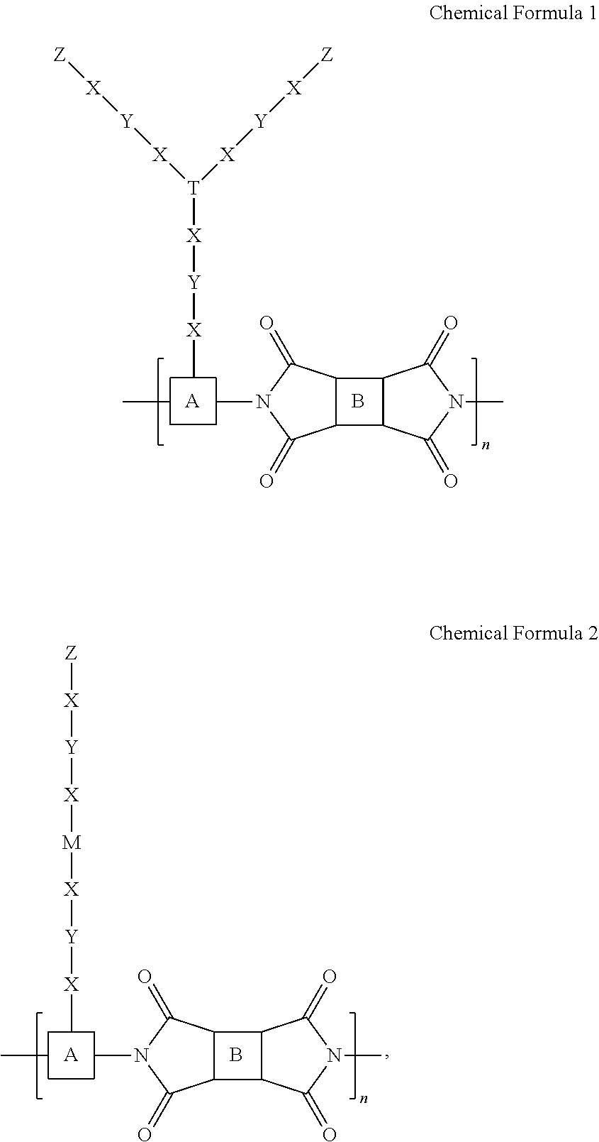
- the first alignment layer and the second alignment layer include at least one compound represented by the following Chemical Formula 1 and Chemical Formula 2, wherein Y or Z is the photoreactor group.
- n is a natural number greater than or equal to 1;
- each X is independently selected from
- n is a natural number greater than or equal to 1.
- each Y is independently selected from
- n is a natural number greater than or equal to 1.
- each Z is independently selected from
- n is a natural number greater than or equal to 1.
- At least one Y in the above Chemical Formula 2 is a
- n is a natural number greater than or equal to 1.
- At least one of the first alignment layer and the second alignment layer include a diamine compound and a dianhydride compound, and the diamine compound and the dianhydride compound are present at a mole ratio of 1:1.
- the common electrode is disposed on the second insulating substrate, and the pixel electrode includes a first subpixel electrode and a second subpixel electrode which include cruciform stem parts and a plurality of fine branch parts extending from the cruciform stem parts.
- the pixel electrode is divided into four sub-regions by the cruciform stem parts.
- the fine branch parts extend in a different direction in each of the sub-regions.
- Neighboring fine branch parts are orthogonal to each other.
- a width of the fine branch part is about 2.5 micrometers ( ⁇ m) to about 5.0 ⁇ m.
- the reactive mesogen includes a reaction initiator, and the reaction initiator is an aryl ester group.
- the photoreactor group includes an acrylate group or a methacrylate group.
- FIG. 1A is a diagram illustrating a process of allowing liquid crystal molecules to have pretilts by using an exemplary alignment layer including a photoreactor group
- FIG. 1B is a schematic view of the exemplary alignment layer.
- FIGS. 2A and 2B are schematic views of an exemplary alignment layer according to the present invention.
- FIGS. 3A and 3B are schematic views of an exemplary embodiment of an alignment layer according to the present invention.
- FIG. 4 is a circuit diagram of one pixel of an exemplary embodiment of a liquid crystal display according to the present invention.
- FIG. 5 is an illustration of a plan view of one pixel in an exemplary liquid crystal display according to the present invention.
- FIG. 6 is a cross-sectional view of the liquid crystal display taken along the line V-V of FIG. 5 .
- FIG. 7 is a diagram illustrating a basic structure of the pixel illustrated in FIG. 5 .
- FIG. 8 is a graph of the instantaneous afterimage of the exemplary liquid display device versus the disappearing time (seconds).
- first,” “second,” “third” etc. may be used herein to describe various elements, components, regions, layers and/or sections, these elements, components, regions, layers and/or sections should not be limited by these terms. These terms are only used to distinguish one element, component, region, layer or section from another element, component, region, layer or section. Thus, “a first element,” “component,” “region,” “layer” or “section” discussed below could be termed a second element, component, region, layer or section without departing from the teachings herein.
- relative terms such as “lower” or “bottom” and “upper” or “top,” may be used herein to describe one element's relationship to another element as illustrated in the Figures. It will be understood that relative terms are intended to encompass different orientations of the device in addition to the orientation depicted in the Figures. For example, if the device in one of the figures is turned over, elements described as being on the “lower” side of other elements would then be oriented on “upper” sides of the other elements. The exemplary term “lower,” can therefore, encompasses both an orientation of “lower” and “upper,” depending on the particular orientation of the figure.
- Exemplary embodiments are described herein with reference to cross section illustrations that are schematic illustrations of idealized embodiments. As such, variations from the shapes of the illustrations as a result, for example, of manufacturing techniques and/or tolerances, are to be expected. Thus, embodiments described herein should not be construed as limited to the particular shapes of regions as illustrated herein but are to include deviations in shapes that result, for example, from manufacturing. For example, a region illustrated or described as flat may, typically, have rough and/or nonlinear features. Moreover, sharp angles that are illustrated may be rounded. Thus, the regions illustrated in the figures are schematic in nature and their shapes are not intended to illustrate the precise shape of a region and are not intended to limit the scope of the present claims.
- FIGS. 5 to 7 a method of orienting liquid crystal molecules 31 to allow them to have a pretilt will be described with reference to FIGS. 5 to 7 along with FIGS. 1A and 1B , FIGS. 2A and 2B , and FIGS. 3A and 3B .
- FIG. 1A is a diagram illustrating a process of allowing liquid crystal molecules to have pretilts by using an alignment layer including a photoreactor group such as with ultraviolet rays
- FIG. 1B is a view illustrating an exemplary embodiment of a structure of the alignment layer.
- FIGS. 2A and 3A are schematic views of a reactive mesogen
- FIG. 2B shows an example of Chemical Formula 1.
- FIG. 3B is an example of Chemical Formula 2 in which —X—Y— of the -M-X—Y—X—Z— portion of the structure is not present.
- alignment layers 11 and 21 including alignment materials are formed on two substrates 110 and 210 , respectively.
- the alignment layers 11 and 21 include a compound including a main chain 12 including a dianhydride and a diamine, and a plurality of side chains which are connected to the main chain 12 .
- the plurality of side chains may each include a reactive mesogen 10 having at least two photoreactor groups 14 , a vertical expression group 13 , and the like.
- a data voltage is applied to a first subpixel electrode 191 a and a second subpixel electrode 191 b
- a common voltage is applied to a common electrode 270 of an upper display panel 200 to generate an electric field in a liquid crystal layer 3 between display panel 100 and upper display panel 200 .
- the liquid crystal molecules 31 of the liquid crystal layer 3 may be tilted in directions parallel with length directions of fine branch parts 194 a , 194 b , 194 c , and 194 d in response to the electric field.
- a direction in which the liquid crystal molecules 31 are tilted in one pixel may be a total of four directions.
- photoreactor groups 14 included in the reactive mesogen react with each other to form a cross-linking portion 15 as illustrated in FIG. 2A .
- the cross-linking portion 15 may have a pretilt.
- the reactive mesogen 10 included in the alignment layers 11 and 21 includes the vertical expression group 13 which is connected to the main chain 12 and the photoreactor group 14 which is connected to the vertical expression group 13 .
- the photoreactor group 14 may also be directly connected to the main chain 12 .
- the reactive mesogen has a pretilt and thus when a voltage is applied to field generating electrodes 191 and 270 , the liquid crystal molecules 31 may be oriented with the pretilt.
- a reaction initiator of a prepolymer may be an aryl ester group.
- the photoreactor group 14 may be an acrylate group or a methacrylate group, but is not limited thereto.
- the reactive mesogen may include the vertical expression group 13 and at least two photoreactor groups 14 , in which the at least two photoreactor groups 14 may be cross-linked by light irradiation to form at least two cross-linking portions 15 , such that mechanical properties of the alignment layers 11 and 21 may be improved.
- alignment layers 11 and 21 will be described in more detail with reference to FIGS. 2A and 2B and FIGS. 3A and 3B .
- the alignment layers 11 and 21 include a compound including the main chain 12 and the plurality of side chains which are connected to the main chain 12 .
- the main chain 12 may include a dianhydride, a diamine, and the like.
- the plurality of side chains includes the reactive mesogen 10 which includes the vertical expression group 13 connected to the main chain 12 and the photoreactor group 14 connected to the vertical expression group 13 .
- some of the plurality of side chains may include only the vertical expression group 13 , and the remaining plurality of side chains may be the reactive mesogen 10 which includes the at least two photoreactor groups 14 connected to the vertical expression group 13 .
- FIGS. 2A to 3A illustrate only the reactive mesogen 10 which includes the vertical expression group 13 and the at least two photoreactor groups 14 connected thereto.
- the at least two photoreactor groups 14 which are included in the reactive mesogen 10 may be connected to one side of the vertical expression group 13 in a “Y” shape, or may be connected to both sides thereof in an “I” shape, and a connection method thereof is not limited.
- the reactive mesogen 10 includes the two photoreactor groups 14 which are located at an end of the reactive mesogen 10 , or as illustrated in FIG. 3A , may include the two photoreactor groups 14 which are located in a length direction of the reactive mesogen.
- the plurality of cross-linking portions 15 may be formed in parallel with each other, and when the photoreactor groups 14 are arranged as illustrated in FIG. 3A , the plurality of cross-linking portions 15 may be separately located from each other.
- the alignment layers 11 and 21 including the reactive mesogen may include at least one compounds represented by the following Chemical Formulas 1 and 2, and the side chain other than the main chain represents the vertical expression group 13 and the photoreactor group 14 which is connected to the vertical expression group 13 .
- each X may be independently selected from
- each Y may be independently selected from
- each Z may be independently selected from
- At least one Y included in the side chain may be
- n is a natural number greater than or equal to 1.
- the photoreactor group may be disposed in parallel with the vertical expression group.
- the Y to Z included in the reactive mesogen may be the photoreactor group. That is, in the case where Y or the Z includes an unsaturated bond over a double bond, the photoreaction may occur.
- Chemical Formula 1 may be the compound as illustrated in FIG. 2B and an example of Chemical Formula 2 may be the compound as illustrated in FIG. 3B , in which —X—Y— of the -M-X—Y—X—Z— portion of Chemical Formula 2 is not present.
- any combination of the foregoing compounds may also be made, and is not limited to those illustrated in FIGS. 2B to 3B .
- one reactive mesogen includes two photoreactor groups
- the invention is not limited thereto, and may include embodiments in which the one reactive mesogen includes at least two photoreactor groups.
- the compound of FIG. 2B may be included in the alignment layer by the following process shown in Chemical Reaction 1:
- the alignment layer may be formed by co-polymerizing the reactive mesogen including the photoreactor groups 14 , a monomer including the vertical expression group 13 and a diamine compound, and a dianhydride compound.
- a mole ratio of the diamine compound and the dianhydride compound may be 1:1.
- the compound of FIG. 3B which is an example of the above Chemical Formula 2 in which —X—Y— of the -M-X—Y—X—Z— portion of Chemical Formula 2 is not present, is not described herein based on a separate schematized chemical reaction formula, but may be derived by substituting the reactive mesogen 10 represented by the above Chemical Formula 2 (illustrated in FIG. 3B ) for the reactive mesogen 10 represented by the above Chemical Formula 1 (illustrated FIG. 2B ) in the above process.
- FIG. 4 is an equivalent circuit diagram of one pixel of an exemplary liquid crystal display.
- one pixel PX of the exemplary liquid crystal display includes a plurality of signal lines which includes a gate line GL transferring a gate signal, a data line DL transferring a data signal, and a voltage dividing reference voltage line RL which transfers a voltage dividing reference voltage, first, second, and third switching elements Qa, Qb, and Qc, respectively, which are connected to the plurality of signal lines, and first and second liquid crystal capacitors Clca and Clcb.
- the first and second switching elements Qa and Qb are each connected to the gate line GL and the data line DL, and the third switching element Qc is connected to an output terminal of the second switching element Qb and the voltage dividing reference voltage line RL.
- the first and second switching elements Qa and Qb are each a three-terminal element, such as a thin film transistor (“TFT”), and control terminals thereof are connected to the gate line GL and input terminals thereof are connected to the data line DL.
- An output terminal of the first switching element Qa is connected to the first liquid crystal capacitor Clca, and an output terminal of the second switching element Qb is connected to input terminals of the second liquid crystal capacitor Clcb and the third switching element Qc.
- the third switching element Qc is also a three-terminal element, such as a thin film transistor, and a control terminal thereof is connected to the gate line GL, an input terminal thereof is connected to the second liquid crystal capacitor Clcb, and an output terminal thereof is connected to the voltage dividing reference voltage line RL.
- a voltage charged in the second liquid crystal capacitor Clcb is divided by the third switching element Qc which is turned on.
- a voltage value which is charged in the second liquid crystal capacitor Clcb is lowered by a difference between the common voltage and the voltage division reference voltage. That is, the voltage which is charged in the first liquid crystal capacitor Clca is higher than the voltage which is charged in the second liquid crystal capacitor Clcb.
- the voltage which is charged in the first liquid crystal capacitor Clca and the voltage which is charged in the second liquid crystal capacitor Clcb are different from each other. Since the voltage of the first liquid crystal capacitor Clca and the voltage of the second liquid crystal capacitor Clcb are different from each other, inclined angles of liquid crystal molecules in the first subpixel and the second subpixel are different from each other, and thus the luminance of the first subpixel and the luminance of the second subpixel are different from each other. Therefore, when the voltage of the first liquid crystal capacitor Clca and the voltage of the second liquid crystal capacitor Clcb are appropriately controlled, an image viewed from a side may maximally approach an image viewed from a front, thereby improving side visibility.
- the second liquid crystal capacitor Clcb and the third switching element Qc are connected to the voltage division reference voltage line RL.
- the second liquid crystal capacitor Clcb may also be connected to a step-down capacitor.
- the liquid crystal display includes the third switching element which includes a first terminal connected to a step-down gate line, a second terminal connected to the second liquid crystal capacitor Clcb, and a third terminal connected to the step-down capacitor to charge a portion of an amount of electric charge charged in the second liquid crystal capacitor Clcb in the step-down capacitor, thereby making the charging voltage between the first liquid crystal capacitor Clca and the second liquid crystal capacitor Clcb different.
- the first and second liquid crystal capacitors Clca and Clcb are connected to different data lines to be applied with different data voltages, thereby allowing the charging voltage between the first and second liquid crystal capacitors Clca and Clcb to be differently set.
- the charging voltage between the first and second liquid crystal capacitors Clca and Clcb may be differently set by several other methods.
- FIG. 5 is a plan view of an example of one pixel of the exemplary liquid crystal display
- FIG. 6 is a cross-sectional view of the liquid crystal display taken along the line V-V of FIG. 5
- FIG. 7 is a plan view illustrating a basic structure of the pixel electrode of the exemplary liquid crystal display.
- an exemplary embodiment of the liquid crystal display includes a lower display panel 100 and an upper display panel 200 facing each other, a liquid crystal layer 3 interposed between the two display panels 100 and 200 , and a pair of polarizers (not illustrated) attached outside the display panels 100 and 200 .
- a gate conductor which includes a gate line 121 and a voltage division reference voltage line 131 is formed on an insulating substrate 110 made of transparent glass, plastic, or the like.
- the gate line 121 includes a wide end (not illustrated) for connection with a first gate electrode 124 a , a second gate electrode 124 b , a third gate electrode 124 c , and another layer or an external driving circuit.
- the voltage division reference voltage line 131 includes first storage electrodes 135 and 136 and a reference electrode 137 .
- Second storage electrodes 138 and 139 are disposed overlapping a second sub-pixel electrode 191 b , but are not connected to the voltage dividing reference voltage line 131 .
- a gate insulating layer 140 is formed on the gate line 121 and the voltage dividing reference voltage line 131 .
- a first semiconductor 154 a , a second semiconductor 154 b , and a third semiconductor 154 c are formed on the gate insulating layer 140 .
- a plurality of ohmic contacts 163 a , 165 a , 163 b , 165 b , 163 c , and 165 c are formed on the semiconductors 154 a , 154 b , and 154 c.
- a plurality of data lines 171 including a first source electrode 173 a and a second source electrode 173 b and a data conductor including a first drain electrode 175 a , a second drain electrode 175 b , a third source electrode 173 c , and a third drain electrode 175 c are formed on the ohmic contacts 163 a , 165 a , 163 b , 165 b , 163 c , and 165 c and the gate insulating layer 140 .
- the data conductor, the semiconductor disposed beneath the data conductor, and the ohmic contact may be simultaneously formed using a single mask.
- the data line 171 includes a wide end (not illustrated) for connection with another layer or an external driving circuit.
- the first gate electrode 124 a , the first source electrode 173 a , and the first drain electrode 175 a form a first thin film transistor (“TFT”) Qa along with the first semiconductor 154 a , and a channel of the first thin film transistor is formed on the first semiconductor 154 a between the first source electrode 173 a and the first drain electrode 175 a .
- the second gate electrode 124 b , the second source electrode 173 b , and the second drain electrode 175 b form one second thin film transistor Qb along with the second semiconductor 154 b , and a channel is formed on the second semiconductor 154 b between the second source electrode 173 b and the second drain electrode 175 b .
- the third gate electrode 124 c , the third source electrode 173 c , and the third drain electrode 175 c form one third thin film transistor Qc along with the third semiconductor 154 c , and the channel is formed on the third semiconductor 154 c between the third source electrode 173 c and the third drain electrode 175 c.
- the second drain electrode 175 b is connected to the third source electrode 173 c and includes a wide expansion 177 .
- a first passivation layer 180 p is formed on the data conductors 171 , 173 c , 175 a , 175 b , and 175 c and the exposed semiconductors 154 a , 154 b , and 154 c .
- the first passivation layer 180 p may include an inorganic insulating layer made of silicon nitride, silicon oxide, or the like.
- the first passivation layer 180 p may prevent a pigment of a color filter 230 from flowing into the exposed semiconductors 154 a , 154 b , and 154 c.
- the color filter 230 is formed on the first passivation layer 180 p .
- the color filter 230 extends in a vertical direction along two data lines which are adjacent to each other.
- a first light blocking member 220 is disposed on the first passivation layer 180 p , the edge of the color filter 230 , and the data line 171 .
- the first light blocking member 220 extends along the data line 171 and is disposed between two adjacent color filters 230 .
- the width of the first light blocking member 220 may be greater than that of the data line 171 .
- the first light blocking member 220 may prevent the incident light from the outside from reflecting off a surface of the data line 171 which is made of metal. Light reflected from the surface of the data line 171 interferes with the light transmitting through the liquid crystal layer 3 and is unable to prevent a contrast ratio of the liquid crystal display from deteriorating.
- a second passivation layer 180 q is formed on the color filter 220 and the first light blocking member 230 .
- the second passivation layer 180 q may include an inorganic insulating layer made of a silicon nitride, a silicon oxide, or the like.
- the second passivation layer 180 q prevents the color filter 230 from lifting and suppresses pollution of the liquid crystal layer 3 due to organic materials such as a solvent inflowing from the color filter 230 , thereby preventing defects, such as an afterimage which may occur at the time of driving the screen, from occurring.
- a third contact hole 185 c which exposes a portion of the reference electrode 137 and a portion of the third drain electrode 175 c , is formed on the first passivation layer 180 p and the second passivation layer 180 q , and the gate insulating layer 140 , in which the third contact hole 185 c is formed, is covered with a connection member 195 .
- the connection member 195 electrically connects between the reference electrode 137 and the third drain electrode 175 c which are exposed through the third contact hole 185 c.
- a plurality of pixel electrodes 191 are formed on the second passivation layer 180 q .
- the pixel electrodes 191 are separated from each other, having the gate line disposed therebetween, and each includes the first sub-pixel electrode 191 a and the second sub-pixel electrode 191 b which are adjacent to each other in a column direction based on the gate line 121 .
- the pixel electrode 191 may be made of a transparent conductive material such as indium tin oxide (“ITO”) and indium zinc oxide (“IZO”).
- ITO indium tin oxide
- IZO indium zinc oxide
- the pixel electrode 191 may also be made of a reflective metal such as aluminum, silver, chromium, or alloys thereof.
- the first sub-pixel electrode 191 a and the second sub-pixel electrode 191 b each include a basic electrode 191 as illustrated in FIG. 7 or at least one variant thereof.
- the first sub-pixel electrode 191 a and the second sub-pixel electrode 191 b are physically and electrically connected to the first drain electrode 175 a and the second drain electrode 175 b through the first and second contact holes 185 a and 185 b , respectively, and are applied with a data voltage from the first drain electrode 175 a and the second drain electrode 175 b .
- some of the data voltage applied to the second drain electrode 175 b is divided by the third source electrode 173 c such that a magnitude of the voltage applied to the first sub-pixel electrode 191 a may be larger than that of the voltage applied to the second sub-pixel electrode 191 b.
- the first sub-pixel electrode 191 a and the second sub-pixel electrode 191 b to which the data voltage is applied generate an electric field along with the common electrode 270 of the upper display panel 200 , thereby determining alignment of liquid crystal molecules of the liquid crystal layer 3 between the two electrodes 191 and 270 .
- the luminance of light passing through the liquid crystal layer 3 along the alignment direction of the liquid crystal molecules determined as described above is changed.
- a second light blocking member 330 is disposed on the pixel electrode 191 .
- the second light blocking member 330 is formed to cover a region in which the first thin film transistor Qa, the second thin film transistor Qb, the third thin film transistor Qc, and the first to third contact holes 185 a , 185 b , and 185 c are disposed, and extends in the same direction as the gate line 121 to overlap a portion of the data line 171 .
- the second light blocking member 330 is disposed to at least partially overlap the two data lines 171 which are disposed at both sides of one pixel region to be able to prevent light from leaking which may occur around the data line 171 and the gate line 121 and prevent light from leaking at a region in which the first thin film transistor Qa, the second thin film transistor Qb, and the third thin film transistor Qc are disposed.
- the first passivation layer 180 p , the color filter 230 , and the second passivation layer 180 q are disposed in the region in which the first thin film transistor Qa, the second thin film transistor Qb, the third thin film transistor Qc, and the first to third contact holes 185 a , 185 b , and 185 c are disposed, thereby easily identifying the positions of the first thin film transistor Qa, the second thin film transistor Qb, the third thin film transistor Qc, and the first to third contact holes 185 a , 185 b , and 185 c.
- the first alignment layer 11 is disposed on the second light blocking member 330 .
- the first alignment layer 11 includes the reactive mesogen 10 including at least two photoreactor groups 14 and may be expressed by the chemical formula illustrated in FIG. 2B or 3B by way of example.
- the mechanical properties may be improved by the alignment layer.
- the common electrode 270 is formed on the insulating substrate 210 .
- the second alignment layer 21 is formed on the common electrode 270 (see for example FIG. 1A ).
- the second alignment layer 21 may be a vertical alignment layer, and may be made of the same material as the foregoing first alignment layer 11 .
- the liquid crystal layer 3 has negative dielectric anisotropy, and the liquid crystal molecules of the liquid crystal layer 3 are aligned so that a major axis thereof is perpendicular to the surfaces of the two display panels 100 and 200 in the state in which no electric field is present.
- the overall shape of the basic electrode 191 is a quadrangle, and includes a cruciform stem part which is configured to include a horizontal stem part 193 and a vertical stem part 192 orthogonal thereto. Further, the basic electrode 191 is divided into a first sub-region Da, a second sub-region Db, a third sub-region Dc, and a fourth sub-region Dd by the horizontal stem part 193 and the vertical stem part 192 , in which each sub-region Da to Dd includes a plurality of first fine branch parts 194 a , a plurality of second fine branch parts 194 b , a plurality of third fine branch parts 194 c , and a plurality of fourth fine branch parts 194 d.
- the first fine branch part 194 a obliquely extends to the left and up from the horizontal stem part 193 or the vertical stem part 192
- the second fine branch part 194 b obliquely extends to the right and up from the horizontal stem part 193 or the vertical stem part 192
- the third fine branch part 194 c extends to the left and down from the horizontal stem part 193 or the vertical stem part 192
- the fourth fine branch part 194 d obliquely extends to the right and down from the horizontal stem part 193 or the vertical stem part 192 .
- the first to fourth fine branch parts 194 a , 194 b , 194 c , and 194 d form an angle of approximately 45° or 135° with respect to the gate line 121 or the horizontal stem part 193 . Further, the fine branch parts 194 a , 194 b , 194 c , and 194 d of two neighboring sub-regions of Da, Db, Dc, and Dd may be orthogonal to each other.
- Widths of the fine branch parts 194 a , 194 b , 194 c , and 194 d may be about 2.5 ⁇ m to about 5.0 ⁇ m, and an interval between the adjacent fine branch parts 194 a , 194 b , 194 c , and 194 d within one sub-region Da, Db, Dc, and Dd may be about 2.5 ⁇ m to about 5.0 ⁇ m.
- the widths of the fine branch parts 194 a , 194 b , 194 c , and 194 d may be widened toward the horizontal stem part 193 or the vertical stem part 192 , and a difference between a portion having the widest width and a portion having the narrowest width in one of the fine branch parts 194 a , 194 b , 194 c , and 194 d may be about 0.2 ⁇ m to about 1.5 ⁇ m.
- the first sub-pixel electrode 191 a and the second sub-pixel electrode 191 b are connected to the first drain electrode 175 a or the second drain electrode 175 b , respectively, through the first and second contact holes 185 a and 186 b , and are applied with a data voltage from the first drain electrode 175 a and the second drain electrode 175 b .
- sides of the first to fourth fine branch parts 194 a , 194 b , 194 c , and 194 d distort an electric field to generate a horizontal component which determines an inclined direction of the liquid crystal molecules 31 .
- the horizontal component of the electric field is substantially horizontal with respect to the sides of the first to fourth fine branch parts 194 a , 194 b , 194 c , and 194 d.
- the liquid crystal molecules 31 are therefore inclined in a direction parallel with a length direction of the fine branch parts 194 a , 194 b , 194 c , and 194 d .
- the one pixel electrode 191 includes the four sub-regions Da, Db, Dc, and Dd in which the length directions of the fine branch parts 194 a , 194 b , 194 c , and 194 d are different from each other, and therefore the direction in which the liquid crystal molecules 31 are inclined is approximately four directions and the liquid crystal layer 3 is formed with four domains in which the alignment direction of the liquid crystal molecules 31 are different on the liquid crystal layer 3 .
- the direction in which the liquid crystal molecules are inclined is various, the reference viewing angle of the liquid crystal display is increased.
- FIG. 8 is a graph showing the instantaneous afterimage versus disappearing time in seconds (sec) for a multipolymerization group and a single polymerization group.
- An exemplary embodiment including the plurality of photoreactor groups is represented by a multiple polymerization group, and a comparative example including a single photoreactor group is represented by a single polymerization group.
- the exemplary alignment layer including the plurality of photoreactor groups has improved mechanical properties, and the liquid crystal display including the exemplary alignment layer has an improved afterimage.
Abstract
Description


wherein n is a natural number greater than or equal to 1;

wherein n is a natural number greater than or equal to 1.

wherein n is a natural number greater than or equal to 1.


wherein n is a natural number greater than or equal to 1.
wherein n is a natural number greater than or equal to 1.


wherein n is a natural number greater than or equal to 1; B may be

each X may be independently selected from
each Y may be independently selected from

wherein n is a natural number greater than or equal to 1; T may independently be N,
M may independently be

and each Z may be independently selected from

wherein n is a natural number greater than or equal to 1. In the compound expressed by the above


Claims (8)


Applications Claiming Priority (2)
| Application Number | Priority Date | Filing Date | Title |
|---|---|---|---|
| KR1020140003550A KR102074956B1 (en) | 2014-01-10 | 2014-01-10 | Liquid crystal display |
| KR10-2014-0003550 | 2014-01-10 |
Publications (2)
| Publication Number | Publication Date |
|---|---|
| US20150198846A1 US20150198846A1 (en) | 2015-07-16 |
| US9454040B2 true US9454040B2 (en) | 2016-09-27 |
Family
ID=53521263
Family Applications (1)
| Application Number | Title | Priority Date | Filing Date |
|---|---|---|---|
| US14/337,379 Active 2034-12-04 US9454040B2 (en) | 2014-01-10 | 2014-07-22 | Liquid crystal display |
Country Status (2)
| Country | Link |
|---|---|
| US (1) | US9454040B2 (en) |
| KR (1) | KR102074956B1 (en) |
Families Citing this family (4)
| Publication number | Priority date | Publication date | Assignee | Title |
|---|---|---|---|---|
| KR102160489B1 (en) | 2014-07-25 | 2020-09-29 | 삼성디스플레이 주식회사 | Fabrication method of display device and display device |
| US9904113B2 (en) | 2014-07-30 | 2018-02-27 | Samsung Display Co., Ltd. | Alignment composition, liquid crystal display panel and method of manufacturing same |
| CN104298038B (en) * | 2014-10-22 | 2017-03-15 | 深圳市华星光电技术有限公司 | Display panels and its array base palte |
| KR102587647B1 (en) * | 2016-05-04 | 2023-10-11 | 삼성디스플레이 주식회사 | Liquid crystal display device and manufacturing method thereof |
Citations (11)
| Publication number | Priority date | Publication date | Assignee | Title |
|---|---|---|---|---|
| US6379758B1 (en) | 1996-07-01 | 2002-04-30 | Merck Patent Gesellschaft Mit Beschrankter Haftung | Liquid crystal display device |
| US6676851B1 (en) | 1999-02-17 | 2004-01-13 | Rolic Ag | Laterally substituted curable liquid crystals |
| JP2005179589A (en) | 2003-12-22 | 2005-07-07 | Fuji Photo Film Co Ltd | Optical element and 2,2'-bithiazole compound |
| JP2005187618A (en) | 2003-12-25 | 2005-07-14 | Asahi Glass Co Ltd | Liquid crystal composition, and method for producing macromolecular liquid crystal using the same |
| JP2007063155A (en) | 2005-08-29 | 2007-03-15 | Hyogo Prefecture | Liquid-crystalline polymerizable low molecular compound, birefringent film using the compound and birefringent cell, and their production methods |
| KR20070092365A (en) | 2006-03-09 | 2007-09-13 | 주식회사 엘지화학 | Polymer for liquid crystal aligning, liquid crystal aligning layer comprising the same and liquid crystal display comprising the same |
| US20100033662A1 (en) | 2008-08-07 | 2010-02-11 | Samsung Electronics Co., Ltd. | Liquid crystal display |
| US20100182556A1 (en) | 2009-01-19 | 2010-07-22 | Samsung Electronics, Co., Ltd. | Liquid crystal display device, method of manufacturing the same and alignment layer composition for the liquid crystal display device |
| US8123977B2 (en) | 2005-11-07 | 2012-02-28 | Lg Chem, Ltd. | Copolymer for liquid crystal alignment, liquid crystal aligning layer including copolymer for liquid crystal alignment, and liquid crystal display including liquid crystal aligning layer |
| US20120172541A1 (en) * | 2010-12-30 | 2012-07-05 | Cheil Industries Inc. | Liquid Crystal Alignment Agent, Liquid Crystal Alignment Film Manufactured Using the Same, and Liquid Crystal Display Device Including the Liquid Crystal Alignment Film |
| US20120229744A1 (en) | 2009-11-09 | 2012-09-13 | Jnc Petrochemical Corporation | Liquid crystal display element, liquid crystal composition, aligning agent, method for producing liquid crystal display element, and use of liquid crystal composition |
Family Cites Families (2)
| Publication number | Priority date | Publication date | Assignee | Title |
|---|---|---|---|---|
| KR20110111212A (en) * | 2010-04-02 | 2011-10-10 | 삼성전자주식회사 | Pixel electrode panel, liquid crystal display panel assembly and methods for manufacturing the same |
| KR20120077467A (en) * | 2010-12-30 | 2012-07-10 | 제일모직주식회사 | Liquid crystal alignment agent, liquid crystal alignment film manufactured using the same, and liquid crystal display device including the liquid crystal alignment film |
-
2014
- 2014-01-10 KR KR1020140003550A patent/KR102074956B1/en active IP Right Grant
- 2014-07-22 US US14/337,379 patent/US9454040B2/en active Active
Patent Citations (11)
| Publication number | Priority date | Publication date | Assignee | Title |
|---|---|---|---|---|
| US6379758B1 (en) | 1996-07-01 | 2002-04-30 | Merck Patent Gesellschaft Mit Beschrankter Haftung | Liquid crystal display device |
| US6676851B1 (en) | 1999-02-17 | 2004-01-13 | Rolic Ag | Laterally substituted curable liquid crystals |
| JP2005179589A (en) | 2003-12-22 | 2005-07-07 | Fuji Photo Film Co Ltd | Optical element and 2,2'-bithiazole compound |
| JP2005187618A (en) | 2003-12-25 | 2005-07-14 | Asahi Glass Co Ltd | Liquid crystal composition, and method for producing macromolecular liquid crystal using the same |
| JP2007063155A (en) | 2005-08-29 | 2007-03-15 | Hyogo Prefecture | Liquid-crystalline polymerizable low molecular compound, birefringent film using the compound and birefringent cell, and their production methods |
| US8123977B2 (en) | 2005-11-07 | 2012-02-28 | Lg Chem, Ltd. | Copolymer for liquid crystal alignment, liquid crystal aligning layer including copolymer for liquid crystal alignment, and liquid crystal display including liquid crystal aligning layer |
| KR20070092365A (en) | 2006-03-09 | 2007-09-13 | 주식회사 엘지화학 | Polymer for liquid crystal aligning, liquid crystal aligning layer comprising the same and liquid crystal display comprising the same |
| US20100033662A1 (en) | 2008-08-07 | 2010-02-11 | Samsung Electronics Co., Ltd. | Liquid crystal display |
| US20100182556A1 (en) | 2009-01-19 | 2010-07-22 | Samsung Electronics, Co., Ltd. | Liquid crystal display device, method of manufacturing the same and alignment layer composition for the liquid crystal display device |
| US20120229744A1 (en) | 2009-11-09 | 2012-09-13 | Jnc Petrochemical Corporation | Liquid crystal display element, liquid crystal composition, aligning agent, method for producing liquid crystal display element, and use of liquid crystal composition |
| US20120172541A1 (en) * | 2010-12-30 | 2012-07-05 | Cheil Industries Inc. | Liquid Crystal Alignment Agent, Liquid Crystal Alignment Film Manufactured Using the Same, and Liquid Crystal Display Device Including the Liquid Crystal Alignment Film |
Also Published As
| Publication number | Publication date |
|---|---|
| KR102074956B1 (en) | 2020-02-10 |
| KR20150083695A (en) | 2015-07-20 |
| US20150198846A1 (en) | 2015-07-16 |
Similar Documents
| Publication | Publication Date | Title |
|---|---|---|
| US20190250467A1 (en) | Liquid crystal display and manufacturing method thereof | |
| US7936407B2 (en) | Array substrate, method of manufacturing the same, display panel having the same, and liquid crystal display apparatus having the same | |
| US10409117B2 (en) | Liquid crystal display | |
| US9664965B2 (en) | Liquid crystal display device with a shielding electrode | |
| US20080018845A1 (en) | Liquid crystal display device and manufacturing method thereof | |
| US10527890B2 (en) | Liquid crystal display and manufacturing method thereof | |
| US9454040B2 (en) | Liquid crystal display | |
| US9372362B2 (en) | Liquid crystal display | |
| US9759965B2 (en) | Liquid crystal display | |
| US20170031213A1 (en) | Liquid crystal display | |
| US9977288B2 (en) | Liquid crystal display | |
| CN105487304B (en) | Liquid crystal display device with a light guide plate | |
| US9720291B2 (en) | Liquid crystal display | |
| US20160195776A1 (en) | Liquid crystal display device | |
| US9298043B2 (en) | Liquid crystal display | |
| US20160195783A1 (en) | Liquid crystal display | |
| US9588376B2 (en) | Liquid crystal display | |
| US9422477B2 (en) | Liquid crystal compositon and liquid crystal display including the same | |
| US10002890B2 (en) | Liquid crystal display | |
| US9671648B2 (en) | Liquid crystal display and method of manufacturing the same | |
| US10620480B2 (en) | Liquid crystal display | |
| US9315668B2 (en) | Liquid crystal display | |
| US20150185533A1 (en) | Liquid crystal display | |
| US9563080B2 (en) | Display device | |
| US9605205B2 (en) | Liquid crystal composition and liquid crystal display including the same |
Legal Events
| Date | Code | Title | Description |
|---|---|---|---|
| AS | Assignment |
Owner name: SAMSUNG DISPLAY CO., LTD., KOREA, REPUBLIC OF Free format text: ASSIGNMENT OF ASSIGNORS INTEREST;ASSIGNOR:LIM, HO;REEL/FRAME:033362/0184 Effective date: 20140430 |
|
| STCF | Information on status: patent grant |
Free format text: PATENTED CASE |
|
| FEPP | Fee payment procedure |
Free format text: PAYOR NUMBER ASSIGNED (ORIGINAL EVENT CODE: ASPN); ENTITY STATUS OF PATENT OWNER: LARGE ENTITY |
|
| MAFP | Maintenance fee payment |
Free format text: PAYMENT OF MAINTENANCE FEE, 4TH YEAR, LARGE ENTITY (ORIGINAL EVENT CODE: M1551); ENTITY STATUS OF PATENT OWNER: LARGE ENTITY Year of fee payment: 4 |
|
| MAFP | Maintenance fee payment |
Free format text: PAYMENT OF MAINTENANCE FEE, 8TH YEAR, LARGE ENTITY (ORIGINAL EVENT CODE: M1552); ENTITY STATUS OF PATENT OWNER: LARGE ENTITY Year of fee payment: 8 |