US9442585B2 - Display device - Google Patents

Display device Download PDF

Info

Publication number
US9442585B2
US9442585B2 US13/678,252 US201213678252A US9442585B2 US 9442585 B2 US9442585 B2 US 9442585B2 US 201213678252 A US201213678252 A US 201213678252A US 9442585 B2 US9442585 B2 US 9442585B2
Authority
US
United States
Prior art keywords
lateral
display device
housing
lateral side
touch sensing
Prior art date
Legal status (The legal status is an assumption and is not a legal conclusion. Google has not performed a legal analysis and makes no representation as to the accuracy of the status listed.)
Active, expires
Application number
US13/678,252
Other versions
US20130321293A1 (en
Inventor
SangRyeon PARK
Sangha Park
Byeongjo Min
Current Assignee (The listed assignees may be inaccurate. Google has not performed a legal analysis and makes no representation or warranty as to the accuracy of the list.)
LG Display Co Ltd
Original Assignee
LG Display Co Ltd
Priority date (The priority date is an assumption and is not a legal conclusion. Google has not performed a legal analysis and makes no representation as to the accuracy of the date listed.)
Filing date
Publication date
Application filed by LG Display Co Ltd filed Critical LG Display Co Ltd
Assigned to LG DISPLAY CO., LTD. reassignment LG DISPLAY CO., LTD. ASSIGNMENT OF ASSIGNORS INTEREST (SEE DOCUMENT FOR DETAILS). Assignors: MIN, BYEONGJO, PARK, SANGHA, PARK, SANGRYEONG
Assigned to LG DISPLAY CO., LTD. reassignment LG DISPLAY CO., LTD. ASSIGNMENT OF ASSIGNORS INTEREST (SEE DOCUMENT FOR DETAILS). Assignors: MIN, BYEONGJO, PARK, SANGHA, PARK, SANGRYEON
Publication of US20130321293A1 publication Critical patent/US20130321293A1/en
Priority to US15/197,270 priority Critical patent/US10101837B2/en
Application granted granted Critical
Publication of US9442585B2 publication Critical patent/US9442585B2/en
Active legal-status Critical Current
Adjusted expiration legal-status Critical

Links

Images

Classifications

    • GPHYSICS
    • G06COMPUTING; CALCULATING OR COUNTING
    • G06FELECTRIC DIGITAL DATA PROCESSING
    • G06F3/00Input arrangements for transferring data to be processed into a form capable of being handled by the computer; Output arrangements for transferring data from processing unit to output unit, e.g. interface arrangements
    • G06F3/01Input arrangements or combined input and output arrangements for interaction between user and computer
    • G06F3/03Arrangements for converting the position or the displacement of a member into a coded form
    • G06F3/041Digitisers, e.g. for touch screens or touch pads, characterised by the transducing means
    • GPHYSICS
    • G06COMPUTING; CALCULATING OR COUNTING
    • G06FELECTRIC DIGITAL DATA PROCESSING
    • G06F1/00Details not covered by groups G06F3/00 - G06F13/00 and G06F21/00
    • G06F1/16Constructional details or arrangements
    • G06F1/1613Constructional details or arrangements for portable computers
    • G06F1/1626Constructional details or arrangements for portable computers with a single-body enclosure integrating a flat display, e.g. Personal Digital Assistants [PDAs]
    • GPHYSICS
    • G06COMPUTING; CALCULATING OR COUNTING
    • G06FELECTRIC DIGITAL DATA PROCESSING
    • G06F3/00Input arrangements for transferring data to be processed into a form capable of being handled by the computer; Output arrangements for transferring data from processing unit to output unit, e.g. interface arrangements
    • G06F3/01Input arrangements or combined input and output arrangements for interaction between user and computer
    • G06F3/03Arrangements for converting the position or the displacement of a member into a coded form
    • G06F3/041Digitisers, e.g. for touch screens or touch pads, characterised by the transducing means
    • G06F3/0412Digitisers structurally integrated in a display
    • GPHYSICS
    • G09EDUCATION; CRYPTOGRAPHY; DISPLAY; ADVERTISING; SEALS
    • G09FDISPLAYING; ADVERTISING; SIGNS; LABELS OR NAME-PLATES; SEALS
    • G09F9/00Indicating arrangements for variable information in which the information is built-up on a support by selection or combination of individual elements
    • GPHYSICS
    • G02OPTICS
    • G02BOPTICAL ELEMENTS, SYSTEMS OR APPARATUS
    • G02B6/00Light guides; Structural details of arrangements comprising light guides and other optical elements, e.g. couplings
    • G02B6/0001Light guides; Structural details of arrangements comprising light guides and other optical elements, e.g. couplings specially adapted for lighting devices or systems
    • G02B6/0011Light guides; Structural details of arrangements comprising light guides and other optical elements, e.g. couplings specially adapted for lighting devices or systems the light guides being planar or of plate-like form
    • G02B6/0033Means for improving the coupling-out of light from the light guide
    • G02B6/005Means for improving the coupling-out of light from the light guide provided by one optical element, or plurality thereof, placed on the light output side of the light guide
    • G02B6/0055Reflecting element, sheet or layer
    • GPHYSICS
    • G02OPTICS
    • G02BOPTICAL ELEMENTS, SYSTEMS OR APPARATUS
    • G02B6/00Light guides; Structural details of arrangements comprising light guides and other optical elements, e.g. couplings
    • G02B6/0001Light guides; Structural details of arrangements comprising light guides and other optical elements, e.g. couplings specially adapted for lighting devices or systems
    • G02B6/0011Light guides; Structural details of arrangements comprising light guides and other optical elements, e.g. couplings specially adapted for lighting devices or systems the light guides being planar or of plate-like form
    • G02B6/0081Mechanical or electrical aspects of the light guide and light source in the lighting device peculiar to the adaptation to planar light guides, e.g. concerning packaging
    • G02B6/0086Positioning aspects
    • G02B6/0088Positioning aspects of the light guide or other optical sheets in the package
    • GPHYSICS
    • G02OPTICS
    • G02FOPTICAL DEVICES OR ARRANGEMENTS FOR THE CONTROL OF LIGHT BY MODIFICATION OF THE OPTICAL PROPERTIES OF THE MEDIA OF THE ELEMENTS INVOLVED THEREIN; NON-LINEAR OPTICS; FREQUENCY-CHANGING OF LIGHT; OPTICAL LOGIC ELEMENTS; OPTICAL ANALOGUE/DIGITAL CONVERTERS
    • G02F1/00Devices or arrangements for the control of the intensity, colour, phase, polarisation or direction of light arriving from an independent light source, e.g. switching, gating or modulating; Non-linear optics
    • G02F1/01Devices or arrangements for the control of the intensity, colour, phase, polarisation or direction of light arriving from an independent light source, e.g. switching, gating or modulating; Non-linear optics for the control of the intensity, phase, polarisation or colour 
    • G02F1/13Devices or arrangements for the control of the intensity, colour, phase, polarisation or direction of light arriving from an independent light source, e.g. switching, gating or modulating; Non-linear optics for the control of the intensity, phase, polarisation or colour  based on liquid crystals, e.g. single liquid crystal display cells
    • G02F1/133Constructional arrangements; Operation of liquid crystal cells; Circuit arrangements
    • G02F1/1333Constructional arrangements; Manufacturing methods
    • G02F1/133308Support structures for LCD panels, e.g. frames or bezels
    • GPHYSICS
    • G02OPTICS
    • G02FOPTICAL DEVICES OR ARRANGEMENTS FOR THE CONTROL OF LIGHT BY MODIFICATION OF THE OPTICAL PROPERTIES OF THE MEDIA OF THE ELEMENTS INVOLVED THEREIN; NON-LINEAR OPTICS; FREQUENCY-CHANGING OF LIGHT; OPTICAL LOGIC ELEMENTS; OPTICAL ANALOGUE/DIGITAL CONVERTERS
    • G02F1/00Devices or arrangements for the control of the intensity, colour, phase, polarisation or direction of light arriving from an independent light source, e.g. switching, gating or modulating; Non-linear optics
    • G02F1/01Devices or arrangements for the control of the intensity, colour, phase, polarisation or direction of light arriving from an independent light source, e.g. switching, gating or modulating; Non-linear optics for the control of the intensity, phase, polarisation or colour 
    • G02F1/13Devices or arrangements for the control of the intensity, colour, phase, polarisation or direction of light arriving from an independent light source, e.g. switching, gating or modulating; Non-linear optics for the control of the intensity, phase, polarisation or colour  based on liquid crystals, e.g. single liquid crystal display cells
    • G02F1/133Constructional arrangements; Operation of liquid crystal cells; Circuit arrangements
    • G02F1/1333Constructional arrangements; Manufacturing methods
    • G02F1/13338Input devices, e.g. touch panels
    • GPHYSICS
    • G02OPTICS
    • G02FOPTICAL DEVICES OR ARRANGEMENTS FOR THE CONTROL OF LIGHT BY MODIFICATION OF THE OPTICAL PROPERTIES OF THE MEDIA OF THE ELEMENTS INVOLVED THEREIN; NON-LINEAR OPTICS; FREQUENCY-CHANGING OF LIGHT; OPTICAL LOGIC ELEMENTS; OPTICAL ANALOGUE/DIGITAL CONVERTERS
    • G02F1/00Devices or arrangements for the control of the intensity, colour, phase, polarisation or direction of light arriving from an independent light source, e.g. switching, gating or modulating; Non-linear optics
    • G02F1/01Devices or arrangements for the control of the intensity, colour, phase, polarisation or direction of light arriving from an independent light source, e.g. switching, gating or modulating; Non-linear optics for the control of the intensity, phase, polarisation or colour 
    • G02F1/13Devices or arrangements for the control of the intensity, colour, phase, polarisation or direction of light arriving from an independent light source, e.g. switching, gating or modulating; Non-linear optics for the control of the intensity, phase, polarisation or colour  based on liquid crystals, e.g. single liquid crystal display cells
    • G02F1/133Constructional arrangements; Operation of liquid crystal cells; Circuit arrangements
    • G02F1/1333Constructional arrangements; Manufacturing methods
    • G02F1/1335Structural association of cells with optical devices, e.g. polarisers or reflectors
    • G02F1/133509Filters, e.g. light shielding masks
    • G02F1/133514Colour filters
    • GPHYSICS
    • G02OPTICS
    • G02FOPTICAL DEVICES OR ARRANGEMENTS FOR THE CONTROL OF LIGHT BY MODIFICATION OF THE OPTICAL PROPERTIES OF THE MEDIA OF THE ELEMENTS INVOLVED THEREIN; NON-LINEAR OPTICS; FREQUENCY-CHANGING OF LIGHT; OPTICAL LOGIC ELEMENTS; OPTICAL ANALOGUE/DIGITAL CONVERTERS
    • G02F1/00Devices or arrangements for the control of the intensity, colour, phase, polarisation or direction of light arriving from an independent light source, e.g. switching, gating or modulating; Non-linear optics
    • G02F1/01Devices or arrangements for the control of the intensity, colour, phase, polarisation or direction of light arriving from an independent light source, e.g. switching, gating or modulating; Non-linear optics for the control of the intensity, phase, polarisation or colour 
    • G02F1/13Devices or arrangements for the control of the intensity, colour, phase, polarisation or direction of light arriving from an independent light source, e.g. switching, gating or modulating; Non-linear optics for the control of the intensity, phase, polarisation or colour  based on liquid crystals, e.g. single liquid crystal display cells
    • G02F1/133Constructional arrangements; Operation of liquid crystal cells; Circuit arrangements
    • G02F1/1333Constructional arrangements; Manufacturing methods
    • G02F1/1335Structural association of cells with optical devices, e.g. polarisers or reflectors
    • G02F1/133528Polarisers
    • GPHYSICS
    • G02OPTICS
    • G02FOPTICAL DEVICES OR ARRANGEMENTS FOR THE CONTROL OF LIGHT BY MODIFICATION OF THE OPTICAL PROPERTIES OF THE MEDIA OF THE ELEMENTS INVOLVED THEREIN; NON-LINEAR OPTICS; FREQUENCY-CHANGING OF LIGHT; OPTICAL LOGIC ELEMENTS; OPTICAL ANALOGUE/DIGITAL CONVERTERS
    • G02F1/00Devices or arrangements for the control of the intensity, colour, phase, polarisation or direction of light arriving from an independent light source, e.g. switching, gating or modulating; Non-linear optics
    • G02F1/01Devices or arrangements for the control of the intensity, colour, phase, polarisation or direction of light arriving from an independent light source, e.g. switching, gating or modulating; Non-linear optics for the control of the intensity, phase, polarisation or colour 
    • G02F1/13Devices or arrangements for the control of the intensity, colour, phase, polarisation or direction of light arriving from an independent light source, e.g. switching, gating or modulating; Non-linear optics for the control of the intensity, phase, polarisation or colour  based on liquid crystals, e.g. single liquid crystal display cells
    • G02F1/133Constructional arrangements; Operation of liquid crystal cells; Circuit arrangements
    • G02F1/1333Constructional arrangements; Manufacturing methods
    • G02F1/1343Electrodes
    • G02F1/134309Electrodes characterised by their geometrical arrangement
    • GPHYSICS
    • G02OPTICS
    • G02FOPTICAL DEVICES OR ARRANGEMENTS FOR THE CONTROL OF LIGHT BY MODIFICATION OF THE OPTICAL PROPERTIES OF THE MEDIA OF THE ELEMENTS INVOLVED THEREIN; NON-LINEAR OPTICS; FREQUENCY-CHANGING OF LIGHT; OPTICAL LOGIC ELEMENTS; OPTICAL ANALOGUE/DIGITAL CONVERTERS
    • G02F1/00Devices or arrangements for the control of the intensity, colour, phase, polarisation or direction of light arriving from an independent light source, e.g. switching, gating or modulating; Non-linear optics
    • G02F1/01Devices or arrangements for the control of the intensity, colour, phase, polarisation or direction of light arriving from an independent light source, e.g. switching, gating or modulating; Non-linear optics for the control of the intensity, phase, polarisation or colour 
    • G02F1/13Devices or arrangements for the control of the intensity, colour, phase, polarisation or direction of light arriving from an independent light source, e.g. switching, gating or modulating; Non-linear optics for the control of the intensity, phase, polarisation or colour  based on liquid crystals, e.g. single liquid crystal display cells
    • G02F1/133Constructional arrangements; Operation of liquid crystal cells; Circuit arrangements
    • G02F1/136Liquid crystal cells structurally associated with a semi-conducting layer or substrate, e.g. cells forming part of an integrated circuit
    • G02F1/1362Active matrix addressed cells
    • G02F1/136286Wiring, e.g. gate line, drain line
    • GPHYSICS
    • G02OPTICS
    • G02FOPTICAL DEVICES OR ARRANGEMENTS FOR THE CONTROL OF LIGHT BY MODIFICATION OF THE OPTICAL PROPERTIES OF THE MEDIA OF THE ELEMENTS INVOLVED THEREIN; NON-LINEAR OPTICS; FREQUENCY-CHANGING OF LIGHT; OPTICAL LOGIC ELEMENTS; OPTICAL ANALOGUE/DIGITAL CONVERTERS
    • G02F1/00Devices or arrangements for the control of the intensity, colour, phase, polarisation or direction of light arriving from an independent light source, e.g. switching, gating or modulating; Non-linear optics
    • G02F1/01Devices or arrangements for the control of the intensity, colour, phase, polarisation or direction of light arriving from an independent light source, e.g. switching, gating or modulating; Non-linear optics for the control of the intensity, phase, polarisation or colour 
    • G02F1/13Devices or arrangements for the control of the intensity, colour, phase, polarisation or direction of light arriving from an independent light source, e.g. switching, gating or modulating; Non-linear optics for the control of the intensity, phase, polarisation or colour  based on liquid crystals, e.g. single liquid crystal display cells
    • G02F1/133Constructional arrangements; Operation of liquid crystal cells; Circuit arrangements
    • G02F1/136Liquid crystal cells structurally associated with a semi-conducting layer or substrate, e.g. cells forming part of an integrated circuit
    • G02F1/1362Active matrix addressed cells
    • G02F1/1368Active matrix addressed cells in which the switching element is a three-electrode device
    • GPHYSICS
    • G06COMPUTING; CALCULATING OR COUNTING
    • G06FELECTRIC DIGITAL DATA PROCESSING
    • G06F1/00Details not covered by groups G06F3/00 - G06F13/00 and G06F21/00
    • G06F1/16Constructional details or arrangements
    • GPHYSICS
    • G06COMPUTING; CALCULATING OR COUNTING
    • G06FELECTRIC DIGITAL DATA PROCESSING
    • G06F1/00Details not covered by groups G06F3/00 - G06F13/00 and G06F21/00
    • G06F1/16Constructional details or arrangements
    • G06F1/1613Constructional details or arrangements for portable computers
    • G06F1/1633Constructional details or arrangements of portable computers not specific to the type of enclosures covered by groups G06F1/1615 - G06F1/1626
    • G06F1/1637Details related to the display arrangement, including those related to the mounting of the display in the housing
    • G06F1/1643Details related to the display arrangement, including those related to the mounting of the display in the housing the display being associated to a digitizer, e.g. laptops that can be used as penpads
    • GPHYSICS
    • G06COMPUTING; CALCULATING OR COUNTING
    • G06FELECTRIC DIGITAL DATA PROCESSING
    • G06F3/00Input arrangements for transferring data to be processed into a form capable of being handled by the computer; Output arrangements for transferring data from processing unit to output unit, e.g. interface arrangements
    • G06F3/01Input arrangements or combined input and output arrangements for interaction between user and computer
    • G06F3/03Arrangements for converting the position or the displacement of a member into a coded form
    • G06F3/041Digitisers, e.g. for touch screens or touch pads, characterised by the transducing means
    • G06F3/047Digitisers, e.g. for touch screens or touch pads, characterised by the transducing means using sets of wires, e.g. crossed wires
    • GPHYSICS
    • G02OPTICS
    • G02FOPTICAL DEVICES OR ARRANGEMENTS FOR THE CONTROL OF LIGHT BY MODIFICATION OF THE OPTICAL PROPERTIES OF THE MEDIA OF THE ELEMENTS INVOLVED THEREIN; NON-LINEAR OPTICS; FREQUENCY-CHANGING OF LIGHT; OPTICAL LOGIC ELEMENTS; OPTICAL ANALOGUE/DIGITAL CONVERTERS
    • G02F1/00Devices or arrangements for the control of the intensity, colour, phase, polarisation or direction of light arriving from an independent light source, e.g. switching, gating or modulating; Non-linear optics
    • G02F1/01Devices or arrangements for the control of the intensity, colour, phase, polarisation or direction of light arriving from an independent light source, e.g. switching, gating or modulating; Non-linear optics for the control of the intensity, phase, polarisation or colour 
    • G02F1/13Devices or arrangements for the control of the intensity, colour, phase, polarisation or direction of light arriving from an independent light source, e.g. switching, gating or modulating; Non-linear optics for the control of the intensity, phase, polarisation or colour  based on liquid crystals, e.g. single liquid crystal display cells
    • G02F1/133Constructional arrangements; Operation of liquid crystal cells; Circuit arrangements
    • G02F1/1333Constructional arrangements; Manufacturing methods
    • G02F1/133308Support structures for LCD panels, e.g. frames or bezels
    • G02F1/133331Cover glasses
    • GPHYSICS
    • G02OPTICS
    • G02FOPTICAL DEVICES OR ARRANGEMENTS FOR THE CONTROL OF LIGHT BY MODIFICATION OF THE OPTICAL PROPERTIES OF THE MEDIA OF THE ELEMENTS INVOLVED THEREIN; NON-LINEAR OPTICS; FREQUENCY-CHANGING OF LIGHT; OPTICAL LOGIC ELEMENTS; OPTICAL ANALOGUE/DIGITAL CONVERTERS
    • G02F2201/00Constructional arrangements not provided for in groups G02F1/00 - G02F7/00
    • G02F2201/12Constructional arrangements not provided for in groups G02F1/00 - G02F7/00 electrode
    • G02F2201/121Constructional arrangements not provided for in groups G02F1/00 - G02F7/00 electrode common or background
    • GPHYSICS
    • G02OPTICS
    • G02FOPTICAL DEVICES OR ARRANGEMENTS FOR THE CONTROL OF LIGHT BY MODIFICATION OF THE OPTICAL PROPERTIES OF THE MEDIA OF THE ELEMENTS INVOLVED THEREIN; NON-LINEAR OPTICS; FREQUENCY-CHANGING OF LIGHT; OPTICAL LOGIC ELEMENTS; OPTICAL ANALOGUE/DIGITAL CONVERTERS
    • G02F2201/00Constructional arrangements not provided for in groups G02F1/00 - G02F7/00
    • G02F2201/12Constructional arrangements not provided for in groups G02F1/00 - G02F7/00 electrode
    • G02F2201/123Constructional arrangements not provided for in groups G02F1/00 - G02F7/00 electrode pixel
    • GPHYSICS
    • G02OPTICS
    • G02FOPTICAL DEVICES OR ARRANGEMENTS FOR THE CONTROL OF LIGHT BY MODIFICATION OF THE OPTICAL PROPERTIES OF THE MEDIA OF THE ELEMENTS INVOLVED THEREIN; NON-LINEAR OPTICS; FREQUENCY-CHANGING OF LIGHT; OPTICAL LOGIC ELEMENTS; OPTICAL ANALOGUE/DIGITAL CONVERTERS
    • G02F2202/00Materials and properties
    • G02F2202/28Adhesive materials or arrangements
    • GPHYSICS
    • G06COMPUTING; CALCULATING OR COUNTING
    • G06FELECTRIC DIGITAL DATA PROCESSING
    • G06F3/00Input arrangements for transferring data to be processed into a form capable of being handled by the computer; Output arrangements for transferring data from processing unit to output unit, e.g. interface arrangements
    • G06F3/01Input arrangements or combined input and output arrangements for interaction between user and computer
    • G06F3/03Arrangements for converting the position or the displacement of a member into a coded form
    • G06F3/041Digitisers, e.g. for touch screens or touch pads, characterised by the transducing means
    • G06F3/044Digitisers, e.g. for touch screens or touch pads, characterised by the transducing means by capacitive means
    • G06F3/0446Digitisers, e.g. for touch screens or touch pads, characterised by the transducing means by capacitive means using a grid-like structure of electrodes in at least two directions, e.g. using row and column electrodes

Definitions

  • the present disclosure relates to a display device, and more particularly, to a display device capable of decreasing a bezel width.
  • a cathode ray tube (CRT) is disadvantageous in that it is heavy and has a large volume. Meanwhile, display devices using flat display panels are advantageous in that they reduce weight and volume. Thus, display devices using flat display panels such as liquid crystal display panel, plasma display panel and organic light-emitting display panel, are generally used.
  • the liquid crystal display panel and the organic light-emitting display panel display images by the use of switching element comprising a thin film transistor.
  • the liquid crystal display panel and the organic light-emitting display panel are widely used for various devices, for example, television, computer monitor, notebook computer, tablet computer, navigation, portable terminal, mobile information device, and etc.
  • FIG. 1 is a perspective view illustrating a related art display device.
  • FIG. 2 is a cross sectional view along I-I′ of FIG. 1 .
  • the related art display device shown in FIG. 1 may be the portable terminal.
  • the related art display device includes a display panel 10 , a backlight unit 20 , a cover glass 30 , a housing member 40 and a touch sensing film 50 .
  • the display panel 10 includes an upper substrate 12 , a lower substrate 14 , a lower polarizing film 16 , and an upper polarizing film 18 .
  • the upper substrate 12 and the lower substrate 14 confronting each other are bonded to each other.
  • the lower polarizing film 16 is adhered to a lower surface of the lower substrate 14
  • the upper polarizing film 18 is adhered to an upper surface of the upper substrate 12 .
  • a panel driver (not shown) is driven, the display panel 10 display a predetermined image.
  • the backlight unit 20 is received in the housing member 40 , wherein the backlight unit 20 emits light to a display area of the display panel 10 .
  • the backlight unit 20 includes a reflective sheet 22 , a light-guiding plate 24 provided on the reflective sheet 22 , a light source (not shown) for emitting light to an incidence surface provided at a lateral side of the light-guiding plate 24 , and a plurality of optical sheet members 26 provided on the light-guiding plate 24 .
  • the cover glass 30 is combined with the housing member 40 at a predetermined interval from an upper surface of the display panel 10 , to thereby protect the display panel 10 .
  • the housing member 40 receives the backlight unit 20 and the display panel 10 therein, and supports the cover glass 30 .
  • the housing member 40 includes a support case 41 for receiving the backlight unit 20 therein; a guide panel 43 combined with the support case 41 , wherein the guide panel 43 supports an edge portion of a lower surface of the display panel 10 ; a rear housing 45 for receiving the support case 41 therein; and a lateral housing 47 combined with the rear housing 45 , wherein the lateral housing 47 supports the cover glass 30 .
  • the lateral housing 47 covers respective lateral sides of the rear housing 45 , the guide panel 43 and the cover glass 30 . Especially, the lateral housing 47 is provided with a step-shaped cover glass supporter 47 b , which is formed in an inner sidewall of an upper surface 47 a of the lateral housing 47 .
  • the cover glass supporter 47 b supports an edge portion of a lower surface of the cover glass 30 , wherein the cover glass supporter 47 b is combined with the edge portion of the lower surface of the cover glass 30 by the use of double-sided tape 49 . Accordingly, a lateral side of the cover glass 30 is covered by the lateral housing 47 , whereby the lateral side of the cover glass 30 is not exposed to the external of the display device. That is, an upper surface of the cover glass 30 is positioned at the same height as the upper surface 47 a of the lateral housing 47 .
  • the touch sensing film 50 is adhered to the lower surface of the cover glass 30 , to thereby sense a user's touch on the cover glass 30 .
  • the cover glass supporter 47 b is formed in the upper surface of the lateral housing 47 , and the cover glass 30 and the lateral housing 47 are combined with each other by the use of double-sided tape 49 , whereby a width (T) of the lateral housing 47 is increased, that is, a bezel width (W) is increased in each of long sides of the display device.
  • a display device comprises a display panel; a cover glass on an upper surface of the display panel; a housing member that receives the display panel, and covers lateral and rear sides of the display panel and a lateral side of the cover glass; and a touch sensing film that seals a gap between the lateral side of the cover glass and the housing member, the touch sensing film adhered to a lower surface of the cover glass.
  • FIG. 1 is a perspective view illustrating a related art display device
  • FIG. 2 is a cross sectional view along I-I′ of FIG. 1 ;
  • FIG. 3 is a perspective view illustrating a display device according to an embodiment of the present invention.
  • FIG. 4 is a cross sectional view illustrating a display device according to the first embodiment of the present invention, which is a cross sectional view along of FIG. 3 ;
  • FIGS. 5 to 8 illustrate various embodiments of touch sensing film shown in FIG. 4 ;
  • FIG. 9 is a cross sectional view illustrating a display device according to the second embodiment of the present invention, which is a cross sectional view along II-II′ of FIG. 3 ;
  • FIG. 10 is a cross sectional view illustrating a display device according to the third embodiment of the present invention, which is a cross sectional view along II-II′ of FIG. 3 ;
  • FIG. 11 is a cross sectional view illustrating a display device according to the fourth embodiment of the present invention, which is a cross sectional view along II-II′ of FIG. 3 ;
  • FIG. 12 is a cross sectional view illustrating a display device according to the fifth embodiment of the present invention, which is a cross sectional view along II-II′ of FIG. 3 .
  • FIG. 3 is a perspective view illustrating a display device according to an embodiment of the present invention.
  • FIG. 4 is a cross sectional view illustrating a display device according to the first embodiment of the present invention, which is a cross sectional view along II-II′ of FIG. 3 .
  • the display device shown in FIG. 3 may be a portable terminal.
  • the display device includes a display panel 110 ; a backlight unit 120 for emitting light to the display panel 110 ; a cover glass 130 provided on the display panel 110 ; a housing member 140 for receiving the backlight unit 120 and the display panel 110 therein, and covering a lateral side of the display panel 110 and a lateral side of the cover glass 130 ; and a touch sensing film 150 adhered to a rear surface of the cover glass 130 , wherein the touch sensing film 150 seals a gap (G) between the lateral side of the cover glass 130 and the housing member 140 .
  • G gap
  • the display panel 110 is received in the housing member 140 , wherein a predetermined image is displayed on the display panel 110 using light emitted from the backlight unit 120 .
  • the display panel 110 includes a lower substrate 112 , an upper substrate 114 , a lower polarizing member 116 , and an upper polarizing member 118 .
  • each pixel is formed every area defined by crossing the gate and data lines.
  • Each pixel may be provided with a thin film transistor (not shown) connected with the gate and data lines, a pixel electrode connected with the thin film transistor, and a common electrode supplied with a common voltage, wherein the common electrode is formed adjacent to the pixel electrode.
  • the common electrode may be formed on the upper substrate 114 .
  • an electric field corresponding to a differential voltage between data voltage and common voltage applied to each pixel is formed to thereby control light transmittance of the liquid crystal layer.
  • a pad (not shown) connected with each signal line, wherein a panel driver (not shown) is combined with the pad (not shown).
  • a gate driving circuit (not shown) for supplying a gate signal (or scan signal) to the gate line.
  • the gate driving circuit to be connected with each gate line is formed during a process for forming the thin film transistor for each pixel.
  • the common electrode to be supplied with the common voltage may be formed on the upper substrate 114 .
  • the upper substrate 114 filters an incident light passing through the liquid crystal layer by the use of color filter, and emits a predetermined-color light to the external, whereby a predetermined color image is displayed on the display panel 110 .
  • the aforementioned structure of the display panel 110 may be changed according to the method for driving liquid crystal of the liquid crystal layer formed between the lower substrate 112 and the upper substrate 114 .
  • the lower polarizing member 116 is adhered to a lower surface of the lower substrate 112 , wherein the lower polarizing member 116 polarizes light emitted from the backlight unit 120 to the display panel 110 .
  • the upper polarizing member 118 may be formed of a polarizing film, adhered to an upper surface of the upper substrate 114 , for polarizing the colored-light emitted to the external through the upper substrate 114 .
  • the upper polarizing member 118 may include an upper polarizing film (not shown), adhered to an upper surface of the upper substrate 114 , for polarizing the colored-light emitted to the external through the upper substrate 114 ; and a retarder film (not shown), adhered to an upper surface of the upper polarizing film, for realizing a separation of images seen in left and right eyes into different polarizing states, that is, a three-dimensional image on the display panel 110 .
  • the backlight unit 120 is received in the housing member 140 , wherein the backlight unit 120 emits the light to the display panel 110 .
  • the backlight unit 120 includes a reflective sheet 122 , a light-guiding plate 124 , a light source member (not shown), and an optical sheet member 126 .
  • the reflective sheet 122 is received in the housing member 140 , wherein the reflective sheet 122 is provided on a lower surface of the light-guiding plate 124 .
  • the reflective sheet 122 reflects the light incident from the light-guiding plate 124 to the display panel 110 .
  • the light-guiding plate 124 is provided on the reflective sheet 122 , wherein the light-guiding plate 124 guides the light emitted from the light source member to a frontal direction.
  • the light-guiding plate 124 may be formed in a plate shape including an incidence surface provided at one lateral side thereof, or may be provided with a lower surface of an inclined shape whose height is gradually decreased from one lateral side to the other lateral side.
  • the light-guiding plate 124 reflects and refracts the light incident on the incidence surface from the light source member, to thereby guide the light to the frontal direction.
  • the light source member is received in the housing member 140 , wherein the light source member confronts the incidence surface, to thereby emit the light to the incidence surface.
  • the light source member may be provided with a plurality of light-emitting diodes.
  • the optical sheet member 126 is provided on the light-guiding plate 124 , wherein the optical sheet member 126 enhances luminance of the light guided to the display panel 110 by the light-guiding plate 124 .
  • the optical sheet member 126 may include at least one diffusion sheet and at least one prism sheet among a lower diffusion sheet, a lower prism sheet, an upper prism sheet and an upper diffusion sheet.
  • the cover glass 130 is provided on the display panel 110 , to thereby protect the display panel 110 .
  • a black coating layer 132 is formed in an edge portion of a lower surface of the cover glass 130 so as to cover remaining areas except a display area of the display panel 110 .
  • lower and upper sides of the cover glass 130 are combined with and covered by lower and upper sides of the housing member 140 .
  • left and right sides of the cover glass 130 are respectively covered by left and right sides of the housing member 140 , there is a predetermined gap (G) between the left side of the cover glass 130 and the left side of the housing member 140 , and between the right side of the cover glass 130 and the right side of the housing member 140 .
  • the housing member 140 receives the backlight unit 120 and the display panel 110 therein, and supports the cover glass 130 .
  • the housing member 140 includes a support case 141 , a guide panel 143 , a rear housing 145 , and a lateral housing 147 .
  • These elements may be formed of a metal material or a plastic material.
  • the these elements are formed of the plastic material suitable for enabling light-weight display device.
  • the support case 141 is received in the rear housing 145 , wherein the support case 141 receives the guide panel 143 and the backlight unit 120 therein, and covers a lateral side of the guide panel 143 .
  • the support case 141 having a U-shaped cross section includes a support plate 141 a , placed onto the rear housing 145 , for supporting the guide panel 143 and the backlight unit 120 ; and a support sidewall 141 b , which is vertically bent from an end of the support plate 141 a , for covering the lateral side of the guide panel 143 .
  • the guide panel 143 is received in the support case 141 , wherein the guide panel 143 supports a peripheral region of a lower surface of the display panel 110 , and defines a receiving position of the backlight unit 120 received in the support case 141 .
  • a lower surface of the guide panel 143 may be adhered to the support plate 141 a of the support case 141 , or adhered to the reflective sheet 122 placed on the support plate 141 a by the use of first double-sided tape 144 a.
  • a second double-sided tape 144 b may be formed between an upper surface of the guide panel 143 and the peripheral region of the lower surface of the display panel 110 .
  • the second double-sided tape 144 b enables to combine the peripheral region of the lower surface of the display panel 110 and the upper surface of the guide panel 143 with each other.
  • the second double-sided tape 144 b may be adhered to a peripheral region of the plurality of optical sheet members 126 as well as the upper surface of the guide panel 143 .
  • the peripheral region of the lower surface of the display panel 110 is combined with the upper surface of the guide panel 143 by the use of second double-sided tape 144 b , but not limited to this structure.
  • the peripheral region of the lower surface of the display panel 110 may be simply placed onto a buffer pad member (not shown) adhered to the upper surface of the guide panel 143 .
  • the rear housing 145 receives the support case 141 therein.
  • the rear housing 145 having a U-shaped cross section supports a lower surface of the support case 141 , and covers some of a lateral side of the support case 141 .
  • the support case 141 may be adhered to a bottom surface of the rear housing 145 by the use of double-sided tape.
  • the lateral housing 147 is combined with an external lateral side of the rear housing 145 , to thereby cover the respective lateral sides of the guide panel 143 , the display panel 110 and the cover glass 130 .
  • the lateral housing 147 and the rear housing 145 may be combined by a hook combination method.
  • a hook-receiving groove may be formed in the external lateral side of the rear housing 145 ; and a hook projection, into which the hook-receiving groove is inserted, may be formed in an inner lateral side of the lateral housing 147 .
  • An upper surface of the lateral housing 147 is positioned at the same height as an upper surface of the cover glass 130 , and an upper inner lateral side of the lateral housing 147 is positioned as close as possible to the lateral side of the cover glass 130 .
  • the upper inner lateral side of the lateral housing 147 is positioned to be in contact with the lateral side of the cover glass 130 . Due to an error of manufacturing process, however, the upper inner lateral side of the lateral housing 147 is provided at a predetermined interval from the lateral side of the cover glass 130 . Accordingly, a predetermined gap (G) is provided between the lateral housing 147 and an edge portion of a long side of the cover glass 130 in each of the left and right sides of the display device. That is, the gap (G) is provided between the upper inner lateral side of the lateral housing 147 and the lateral side of the cover glass 130 .
  • each of short sides of the cover glass 130 that is, each of upper and lower sides of the cover glass 130 is placed in a step-shaped cover glass supporter (See the cover glass supporter of FIG. 2 ) which is provided in each of upper and lower sides of the lateral housing 147 . Accordingly, a predetermined gap (G) is not formed between an edge portion of the short side of the cover glass 130 and the lateral housing 147 in each of upper and lower sides of the display device.
  • the aforementioned lateral housing 147 does not support the lower edge portion of the cover glass 130 , and the lateral housing 147 is positioned as close as possible to the lateral side of the cover glass 130 , to thereby obtain a relatively thin width (W). Owing to the relatively thin width (W) of the lateral housing 147 , it is possible to decrease a width in each of both lateral sides of the display device, that is, to decrease a bezel width. However, foreign matters such as dust or moist may penetrate into the inside of the display device through the predetermined gap (G) between the upper inner lateral side of the lateral housing 147 and the lateral side of the cover glass 130 , and light emitted from the backlight unit 120 may be leaking to the external through the predetermined gap (G). Accordingly, the gap (G) is sealed by extending the left and right lateral sides of the touch sensing film 150 .
  • the touch sensing film 150 is adhered to the lower surface of the cover glass 130 , and is placed onto the upper polarizing member 118 of the display panel 110 .
  • the touch sensing film 150 may be adhered to the entire area of the lower surface of the cover glass 130 by the use of optical clean adhesive, and simultaneously adhered to the entire area of the upper surface of the upper polarizing film 118 .
  • the touch sensing film 150 may be adhered to the lower surface of the cover glass 130 by a manual labor or a lamination process.
  • the touch sensing film 150 functions as a touch sensing means so as to sense a user's touch on the cover glass 130 .
  • the touch sensing film 150 seals the aforementioned gap (G) between the lateral side of the cover glass 130 and the housing member 140 .
  • the touch sensing film 150 includes a touch sensing area, and the touch sensing film 150 includes first and second extending portions 154 a and 154 b for sealing the gap (G), wherein each of the first and second extending portions 154 a and 154 b is extended to be longer than each of the left and right sides of the cover glass 130 .
  • the first extending portion 154 a is extended to a predetermined length from the left lateral side of the touch sensing film 150 , and is also bent to be combined with the housing member 140 , that is, the external lateral side of the left sidewall of the support case 141 .
  • the first extending portion 154 a may be adhered to the external lateral side of the left sidewall of the support case 141 by the use of first adhesive member 155 a .
  • the first adhesive member 155 a may be a double-sided tape.
  • the second extending portion 154 b is extended to a predetermined length from the right lateral side of the touch sensing film 150 , and is also bent to be combined with the housing member 140 , that is, the external lateral side of the right sidewall of the support case 141 .
  • the second extending portion 154 b may be adhered to the external lateral side of the right sidewall of the support case 141 by the use of second adhesive member 155 b .
  • the second adhesive member 155 b may be a double-sided tape.
  • FIG. 5 is a perspective view illustrating the touch sensing film shown in FIG. 4 .
  • the touch sensing film 150 includes a touch sensor 152 , and the first and second extending portions 154 a and 154 b.
  • the touch sensor 152 is adhered to the lower surface of the cover glass 130 , wherein the touch sensor 152 is overlapped with the display area of the display panel 110 .
  • the touch sensor 152 includes a lower film 150 a and an upper film 150 b which are bonded to each other, wherein the lower film 150 a and the upper film 150 b has a size corresponding to a size of the upper substrate 114 or cover glass 130 .
  • first sensing electrode lines (SL 1 ) formed at fixed intervals in a first direction.
  • Each of the first sensing electrode lines (SL 1 ) may be supplied with a first sensing voltage signal from a touch driver (not shown).
  • the plurality of first sensing electrode lines (SL 1 ) may function as signal-transmitting electrodes.
  • each of the second sensing electrode lines (SL 2 ) may be supplied with a second sensing voltage signal from the touch driver.
  • the plurality of second sensing electrode lines (SL 2 ) may function as signal-transmitting electrodes.
  • a driving connector 150 c which is electrically connected with the plurality of first sensing electrode lines (SL 1 ), and also electrically connected with the plurality of second sensing electrode lines (SL 2 ).
  • the driving connector 150 c having a predetermined length is protruding from one side of the lower film 150 a or upper film 150 b , and the driving connector 150 c is connected with the touch driver, whereby the driving connector 150 c supplies the first and second sensing voltage signals from the touch driver to the plurality of first sensing electrode lines (SL 1 ) and the plurality of second sensing electrode lines (SL 2 ).
  • the touch driver senses a change of capacitance value formed among the plurality of first sensing electrode lines (SL 1 ) and the plurality of second sensing electrodes lines (SL 2 ), wherein the first and second sensing electrode lines (SL 1 and SL 2 ) cross each other, to thereby sense whether or not there is the user's touch.
  • the plurality of second sensing electrode line (SL 2 ) may be formed on the lower film 150 a .
  • each of the plurality of second sensing electrode lines (SL 2 ) may be formed between each of the plurality of first sensing electrode lines (SL 1 ).
  • a shield line may be formed between the first sensing electrode line (SL 1 ) and the second sensing electrode line (SL 2 ).
  • the first extending portion 154 a is extended to be longer than the cover glass 130 from the left side of the touch sensor 152 , that is, the respective left sides of the lower film 150 a and upper film 150 b . Also, the first extending portion 154 a is bent to cover the left side of the display panel 110 , and is then adhered to the housing member 140 , that is, the external lateral side of the left sidewall of the support case 141 by the use of first adhesive member 155 a . Thus, the first extending portion 154 a is closely adhered to the inner lateral side of the lateral housing 147 , to thereby seal the gap (G) between the left long side of the cover glass 130 and the lateral side of the housing 147 . Accordingly, it is possible to prevent foreign matters such as dust or moist from penetrating into the inside of the display device through the gap (G).
  • the second extending portion 154 b is extended to be longer than the cover glass 130 from the right side of the touch sensor 152 , that is, the respective right sides of the lower film 150 a and upper film 150 b . Also, the second extending portion 154 b is bent to cover the right side of the display panel 110 , and is then adhered to the housing member 140 , that is, the external lateral side of the right sidewall of the support case 141 by the use of second adhesive member 155 b . Thus, the second extending portion 154 b is closely adhered to the inner lateral side of the lateral housing 147 , to thereby seal the gap (G) between the right long side of the cover glass 130 and the lateral side of the housing 147 . Accordingly, it is possible to prevent foreign matters such as dust or moist from penetrating into the inside of the display device through the gap (G).
  • the touch sensing film 150 may further include a light-leakage prevention member 156 in each of the inner lateral sides of the first and second extending portions 154 a and 154 b confronting the respective lateral sides of the display panel 110 .
  • the light-leakage prevention member 156 may be formed by a coating layer coated on the respective inner lateral sides of the first and second extending portions 154 a and 154 b , or a tape adhered to the respective inner lateral sides of the first and second extending portions 154 a and 154 b .
  • the light-leakage prevention member 156 may be formed of black-colored coating resin or tape.
  • the first and second extending portions 154 a and 154 b extend from the lower film 150 a and the upper film 150 b , but it is not limited to this structure. That is, the first and second extending portions 154 a and 154 b may be formed only of the lower film 150 a extended from the both lateral sides of the touch sensor 152 , as shown in FIG. 7 ; or the first and second extending portions 154 a and 154 b may be formed only of the upper film 150 b extended from the both lateral sides of the touch sensor 152 , as shown in FIG. 8 .
  • the first and second extending portions 154 a and 154 b extend from the upper film 150 b .
  • the first and second extending portions 154 a and 154 b extend from the relatively-thin film between the lower film 150 a and the upper film 150 b , preferably.
  • the aforementioned light-leakage prevention member 156 is formed in each of the inner lateral sides of the first and second extending portions 154 a and 154 b.
  • the cover glass 130 with the touch sensing film 150 adhered thereto is placed on the upper surface of the display panel 110 , and the extended touch sensing film 150 seals the gap (G) between the lateral side of the cover glass 130 and the housing member 140 , that is, the lateral housing 147 , whereby the width (W) of the lateral housing 147 is decreased, thereby decreasing the bezel width (W) of the both lateral sides.
  • the cover glass 130 is not supported by the lateral housing 147 of the housing member 140 , whereby the width (W) of the lateral housing 147 becomes thin, to thereby the bezel width (W) of the both lateral sides.
  • FIG. 9 is a cross sectional view illustrating a display device according to the second embodiment of the present invention, which is a cross sectional view along II-II′ of FIG. 3 .
  • the display device according to the second embodiment of the present invention includes a display panel 110 , a backlight unit 120 , a cover glass 130 , a housing member 140 , and a touch sensing film 150 . Except a structure of the housing member 140 , the display device according to the second embodiment of the present invention is identical in structure to the display device according to the first embodiment of the present invention shown in FIGS. 3 to 8 . Thus, wherever possible, the same reference numbers will be used throughout the drawings to refer to the same or like parts, and a detailed explanation for the same parts will be omitted.
  • the housing member 140 includes a support case 141 , a guide panel 143 , and a housing cover 245 . These elements may be formed of a metal material or a plastic material. Preferably, the these elements are formed of the plastic material suitable for enabling light-weight display device.
  • the support case 141 and the guide panel 143 are the same as those of the aforementioned display device according to the first embodiment of the present invention, whereby a detailed explanation for the support case 141 and the guide panel 143 will be omitted.
  • the housing cover 245 receives the support case 141 therein, and covers the respective lateral sides of the support case 141 , the display panel 110 , and the cover glass 130 .
  • the housing cover 245 includes a rear cover 245 a and a lateral cover 245 b.
  • the rear cover 245 a supports a lower surface of the support case 141 .
  • the lower surface of the support case 141 may be adhered to the rear cover 245 a by the use of double-sided tape.
  • the lateral cover 245 b is formed by vertically bending an end portion of the rear cover 245 a .
  • the lateral cover 245 b covers the respective lateral sides of the support case 141 , the display panel 110 and the cover glass 130 .
  • a predetermined gap is formed between an upper inner lateral side of the lateral cover 245 b and a lateral side of the cover glass 130 , wherein the gaps is sealed by the use of extending portions 154 a and 154 b of the touch sensing film 150 .
  • a function of the lateral cover 245 b is the same as that of the aforementioned lateral housing 147 shown in FIG. 4 . Accordingly, the display device according to the second embodiment of the present invention is formed by removing the lateral housing 147 of the first embodiment of the present invention, whereby the display device according to the second embodiment of the present invention is provided with the decreased number of elements.
  • FIG. 10 is a cross sectional view illustrating a display device according to the third embodiment of the present invention, which is a cross sectional view along II-II′ of FIG. 3 .
  • the display device according to the third embodiment of the present invention includes a display panel 110 , a backlight unit 120 , a cover glass 130 , a housing member 140 , and a touch sensing film 150 . Except a structure of the touch sensing film 150 , the display device according to the third embodiment of the present invention is identical in structure to the display device according to the first embodiment of the present invention shown in FIGS. 3 to 8 . Thus, wherever possible, the same reference numbers will be used throughout the drawings to refer to the same or like parts, and a detailed explanation for the same parts will be omitted.
  • the touch sensing film 150 is extended and adhered to the support sidewall 141 b of the support case 141 .
  • the touch sensing film 150 is extended and adhered to a lower edge portion of a support case 141 .
  • respective extending portions 154 a and 154 b of the touch sensing film 150 are extended from both lateral sides of a touch sensor (See ‘ 152 ’ of FIG. 5 ), and are then adhered to the lower edge portions of the left and right sides of the support case 141 .
  • the respective extending portions 154 a and 154 b include first bending portions (BP 1 ) for covering the lateral sides of the display panel 110 , and support sidewalls 141 b of the left and right sides (or long side) of the support case 141 ; and second bending portions (BP 2 ) for covering the lower edge portions of the left and right sides of a support plate 141 a .
  • the respective second bending portions (BP 2 ) are adhered to the lower edge portion of the support plate 141 a by the use of adhesive members 155 a and 155 b.
  • the support case 141 is combined with a bottom surface of a rear housing 145 by the use of combining member 149 .
  • the combining member 149 may be a double-sided tape, an adhesive, or a plurality of screws.
  • the housing member 140 may include the support case 141 , a guide panel 143 , the rear housing 145 and the lateral housing 147 , in the same manner as the display device according to the first embodiment of the present invention shown in FIG. 4 ; or the housing member 140 may include the support case 141 , a guide panel 143 and a housing cover 240 , in the same manner as the display device according to the second embodiment of the present invention shown in FIG. 9 .
  • FIG. 11 is a cross sectional view illustrating a display device according to the fourth embodiment of the present invention, which is a cross sectional view along II-II′ of FIG. 3 .
  • the display device according to the fourth embodiment of the present invention includes a display panel 110 , a backlight unit 120 , a cover glass 130 , a housing member 440 , and a touch sensing film 150 . Except a structure of the housing member 440 , the display device according to the fourth embodiment of the present invention is identical in structure to the display device according to the first embodiment of the present invention shown in FIGS. 3 to 8 . Thus, wherever possible, the same reference numbers will be used throughout the drawings to refer to the same or like parts, and a detailed explanation for the same parts will be omitted.
  • the housing member 440 includes a guide panel 143 , a rear housing 145 , and a lateral housing 147 .
  • the housing member 440 may be obtained by removing the support case (See ‘ 141 ’ of FIG. 4 ) from the housing member 140 of the display device according to the first embodiment of the present invention.
  • the guide panel 143 is adhered to a reflective sheet 122 of the backlight unit 120 by the use of first double-sided tape 444 a . Meanwhile, the guide panel 143 may be adhered to a bottom surface of the rear housing 145 by the use of first double-sided tape 444 a.
  • the rear housing 145 receives the backlight unit 120 and the guide panel 130 therein.
  • the rear housing 145 having a U-shaped cross section supports the reflective sheet 122 of the backlight unit 120 , and covers some area of a lateral side of the guide panel 130 .
  • the lateral housing 147 is combined with an external lateral side of the rear housing 145 , to thereby cover respective lateral sides of the guide panel 143 , the display panel 110 , and the cover glass 130 .
  • the lateral housing 147 and the rear housing 145 may be combined by a hook combination method.
  • First and second extending portions 154 a and 154 b of the touch sensing film 150 are extended to cover the lateral sides of the display panel 110 and the guide panel 143 , and are then adhered to an inner lateral side of the lateral housing 147 by the use of first and second adhesive members 455 a and 455 b , to thereby seal a gap between the respective lateral sides of the lateral housing 147 and the cover glass 130 .
  • the display device according to the fourth embodiment of the present invention is provided with the housing member 440 obtained by removing the support case (See ‘ 141 ’ of FIG. 4 ) from the housing member 140 of the display device according to the first embodiment of the present invention, so that it is possible to decrease the number of elements in the display device.
  • FIG. 12 is a cross sectional view illustrating a display device according to the fifth embodiment of the present invention, which is a cross sectional view along II-II′ of FIG. 3 .
  • the display device according to the fifth embodiment of the present invention includes a display panel 110 , a backlight unit 120 , a cover glass 130 , a housing member 140 , and a touch sensing film 150 . Except a structure of the housing member 140 , the display device according to the fifth embodiment of the present invention is identical in structure to the display device according to the fourth embodiment of the present invention shown in FIG. 11 . Thus, wherever possible, the same reference numbers will be used throughout the drawings to refer to the same or like parts, and a detailed explanation for the same parts will be omitted.
  • the housing member 140 includes a guide panel 143 and a housing cover 545 .
  • the guide panel 143 is the same as that of the display device according to the fourth embodiment of the present invention, whereby a detailed explanation for the guide panel 143 will be omitted.
  • the housing cover 545 receives the backlight unit 120 and the guide panel 143 therein, and covers respective lateral sides of the guide panel 143 , the display panel 110 and the cover glass 130 .
  • the housing cover 545 includes a rear cover 545 a and a lateral cover 545 b.
  • the rear cover 545 a supports the backlight unit 120 and the guide panel 143 .
  • a reflective sheet 122 of the backlight unit 120 may be adhered to the rear cover 545 a by the use of double-sided tape.
  • the lateral cover 545 b is formed by vertically bending an end portion of the rear cover 545 a .
  • the lateral cover 545 b covers the respective lateral sides of the guide panel 143 , the display panel 110 and the cover glass 130 .
  • a gap is formed between an upper inner lateral side of the lateral cover 545 b and a lateral side of the cover glass 130 , wherein the gaps is sealed by extending portions 154 a and 154 b of the touch sensing film 150 .
  • a function of the lateral cover 545 b is the same as that of the aforementioned lateral housing 147 shown in FIG. 11 . Accordingly, the display device according to the fifth embodiment of the present invention is formed by removing the lateral housing 147 of the fourth embodiment of the present invention, whereby the display device according to the fifth embodiment of the present invention is provided with the decreased number of elements.
  • the display devices according to the embodiments of the present invention are mainly LCD devices with the backlight unit 120 provided therein, but it is not limited to the LCD devices.
  • the display devices according to the embodiments of the present invention may be various flat display devices such as organic light-emitting display (OLED) devices.
  • the display device of the OLED device may include a display panel comprising an organic light-emitting device on an upper substrate or a lower substrate, whereby a predetermined image is displayed according as the organic light-emitting device is driven.
  • the backlight unit may be removed from the display device shown in FIG. 4 . If needed, the support case of the housing member and/or the guide panel may be removed from the display device shown in FIG. 4 .
  • the display devices according to the embodiments of the present invention may be applied to not only the portable terminal shown in FIG. 3 but also a television, a computer monitor, a tablet computer, various mobile information devices, and a display area of notebook computer.
  • the both lateral sides of the cover glass are not combined with the lateral housing member, whereby the width of the lateral housing is decreased, to thereby decrease the bezel width in the both lateral sides of the display device.
  • the touch sensing film adhered to the lower surface of the cover glass is extended to seal the gap between the lateral side of the cover glass and the housing member, so that it is possible to prevent the foreign matters such as dust or moist from penetrating into the inside of the display device through the gap, thereby improving quality and endurance of the display device.

Abstract

Disclosed is a display device capable of decreasing a bezel width, wherein the display device comprises a display panel; a cover glass on an upper surface of the display panel; a housing member for receiving the display panel, and covering lateral and rear sides of the display panel and a lateral side of the cover glass; and a touch sensing film for sealing a gap between the lateral side of the cover glass and the housing member, the touch sensing film adhered to a lower surface of the cover glass.

Description

CROSS REFERENCE TO RELATED APPLICATIONS
This application claims the benefit of the Korean Patent Application No. 10-2012-0056762 filed on May 29, 2012, which is hereby incorporated by reference as if fully set forth herein.
BACKGROUND
1. Field of the Disclosure
The present disclosure relates to a display device, and more particularly, to a display device capable of decreasing a bezel width.
2. Discussion of the Related Art
A cathode ray tube (CRT) is disadvantageous in that it is heavy and has a large volume. Meanwhile, display devices using flat display panels are advantageous in that they reduce weight and volume. Thus, display devices using flat display panels such as liquid crystal display panel, plasma display panel and organic light-emitting display panel, are generally used.
The liquid crystal display panel and the organic light-emitting display panel display images by the use of switching element comprising a thin film transistor. The liquid crystal display panel and the organic light-emitting display panel are widely used for various devices, for example, television, computer monitor, notebook computer, tablet computer, navigation, portable terminal, mobile information device, and etc.
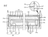
FIG. 1 is a perspective view illustrating a related art display device. FIG. 2 is a cross sectional view along I-I′ of FIG. 1. In this case, the related art display device shown in FIG. 1 may be the portable terminal.
Referring to FIGS. 1 and 2, the related art display device includes a display panel 10, a backlight unit 20, a cover glass 30, a housing member 40 and a touch sensing film 50.
The display panel 10 includes an upper substrate 12, a lower substrate 14, a lower polarizing film 16, and an upper polarizing film 18. In this case, the upper substrate 12 and the lower substrate 14 confronting each other are bonded to each other. Also, the lower polarizing film 16 is adhered to a lower surface of the lower substrate 14, and the upper polarizing film 18 is adhered to an upper surface of the upper substrate 12. As a panel driver (not shown) is driven, the display panel 10 display a predetermined image.
The backlight unit 20 is received in the housing member 40, wherein the backlight unit 20 emits light to a display area of the display panel 10. For this, the backlight unit 20 includes a reflective sheet 22, a light-guiding plate 24 provided on the reflective sheet 22, a light source (not shown) for emitting light to an incidence surface provided at a lateral side of the light-guiding plate 24, and a plurality of optical sheet members 26 provided on the light-guiding plate 24.
The cover glass 30 is combined with the housing member 40 at a predetermined interval from an upper surface of the display panel 10, to thereby protect the display panel 10.
The housing member 40 receives the backlight unit 20 and the display panel 10 therein, and supports the cover glass 30. For this, the housing member 40 includes a support case 41 for receiving the backlight unit 20 therein; a guide panel 43 combined with the support case 41, wherein the guide panel 43 supports an edge portion of a lower surface of the display panel 10; a rear housing 45 for receiving the support case 41 therein; and a lateral housing 47 combined with the rear housing 45, wherein the lateral housing 47 supports the cover glass 30.
The lateral housing 47 covers respective lateral sides of the rear housing 45, the guide panel 43 and the cover glass 30. Especially, the lateral housing 47 is provided with a step-shaped cover glass supporter 47 b, which is formed in an inner sidewall of an upper surface 47 a of the lateral housing 47.
The cover glass supporter 47 b supports an edge portion of a lower surface of the cover glass 30, wherein the cover glass supporter 47 b is combined with the edge portion of the lower surface of the cover glass 30 by the use of double-sided tape 49. Accordingly, a lateral side of the cover glass 30 is covered by the lateral housing 47, whereby the lateral side of the cover glass 30 is not exposed to the external of the display device. That is, an upper surface of the cover glass 30 is positioned at the same height as the upper surface 47 a of the lateral housing 47.
The touch sensing film 50 is adhered to the lower surface of the cover glass 30, to thereby sense a user's touch on the cover glass 30.
In the related art display device, the cover glass supporter 47 b is formed in the upper surface of the lateral housing 47, and the cover glass 30 and the lateral housing 47 are combined with each other by the use of double-sided tape 49, whereby a width (T) of the lateral housing 47 is increased, that is, a bezel width (W) is increased in each of long sides of the display device.
SUMMARY
A display device comprises a display panel; a cover glass on an upper surface of the display panel; a housing member that receives the display panel, and covers lateral and rear sides of the display panel and a lateral side of the cover glass; and a touch sensing film that seals a gap between the lateral side of the cover glass and the housing member, the touch sensing film adhered to a lower surface of the cover glass.
It is to be understood that both the foregoing general description and the following detailed description of the present invention are exemplary and explanatory and are intended to provide further explanation of the invention as claimed.
BRIEF DESCRIPTION OF THE DRAWINGS
The accompanying drawings, which are included to provide a further understanding of the invention and are incorporated in and constitute a part of this application, illustrate embodiment(s) of the invention and together with the description serve to explain the principle of the invention. In the drawings:
FIG. 1 is a perspective view illustrating a related art display device;
FIG. 2 is a cross sectional view along I-I′ of FIG. 1;
FIG. 3 is a perspective view illustrating a display device according to an embodiment of the present invention;
FIG. 4 is a cross sectional view illustrating a display device according to the first embodiment of the present invention, which is a cross sectional view along of FIG. 3;
FIGS. 5 to 8 illustrate various embodiments of touch sensing film shown in FIG. 4;
FIG. 9 is a cross sectional view illustrating a display device according to the second embodiment of the present invention, which is a cross sectional view along II-II′ of FIG. 3;
FIG. 10 is a cross sectional view illustrating a display device according to the third embodiment of the present invention, which is a cross sectional view along II-II′ of FIG. 3;
FIG. 11 is a cross sectional view illustrating a display device according to the fourth embodiment of the present invention, which is a cross sectional view along II-II′ of FIG. 3; and
FIG. 12 is a cross sectional view illustrating a display device according to the fifth embodiment of the present invention, which is a cross sectional view along II-II′ of FIG. 3.
DETAILED DESCRIPTION OF THE EXEMPLARY EMBODIMENTS
Reference will now be made in detail to the exemplary embodiments of the present invention, examples of which are illustrated in the accompanying drawings. Wherever possible, the same reference numbers will be used throughout the drawings to refer to the same or like parts.
Hereinafter, a display device according to the present disclosure will be described with reference to the accompanying drawings.
FIG. 3 is a perspective view illustrating a display device according to an embodiment of the present invention. FIG. 4 is a cross sectional view illustrating a display device according to the first embodiment of the present invention, which is a cross sectional view along II-II′ of FIG. 3. Herein, the display device shown in FIG. 3 may be a portable terminal.
Referring to FIGS. 3 and 4, the display device according to the first embodiment of the present invention includes a display panel 110; a backlight unit 120 for emitting light to the display panel 110; a cover glass 130 provided on the display panel 110; a housing member 140 for receiving the backlight unit 120 and the display panel 110 therein, and covering a lateral side of the display panel 110 and a lateral side of the cover glass 130; and a touch sensing film 150 adhered to a rear surface of the cover glass 130, wherein the touch sensing film 150 seals a gap (G) between the lateral side of the cover glass 130 and the housing member 140.
The display panel 110 is received in the housing member 140, wherein a predetermined image is displayed on the display panel 110 using light emitted from the backlight unit 120. For this, the display panel 110 includes a lower substrate 112, an upper substrate 114, a lower polarizing member 116, and an upper polarizing member 118.
On the lower substrate 112 of the display panel 110, there are a plurality of gate lines (not shown), a plurality of data lines (not shown), and a plurality of pixels (not shown), wherein each pixel is formed every area defined by crossing the gate and data lines. Each pixel may be provided with a thin film transistor (not shown) connected with the gate and data lines, a pixel electrode connected with the thin film transistor, and a common electrode supplied with a common voltage, wherein the common electrode is formed adjacent to the pixel electrode. According to a method for driving liquid crystal of a liquid crystal layer, the common electrode may be formed on the upper substrate 114. On the lower substrate 112, an electric field corresponding to a differential voltage between data voltage and common voltage applied to each pixel is formed to thereby control light transmittance of the liquid crystal layer.
At an edge region of a lateral side of the lower substrate 112, there is a pad (not shown) connected with each signal line, wherein a panel driver (not shown) is combined with the pad (not shown).
In a non-display area of one short side or both short sides of the lower substrate 112, there is a gate driving circuit (not shown) for supplying a gate signal (or scan signal) to the gate line. The gate driving circuit to be connected with each gate line is formed during a process for forming the thin film transistor for each pixel.
On the upper substrate 114, there is a color filter corresponding to each pixel of the lower substrate 112. Then, the lower substrate 112 and the upper substrate 114 confronting each other are bonded to each other, and the liquid crystal layer (not shown) is interposed therebetween. According to the method for driving liquid crystal of the liquid crystal layer, the common electrode to be supplied with the common voltage may be formed on the upper substrate 114. The upper substrate 114 filters an incident light passing through the liquid crystal layer by the use of color filter, and emits a predetermined-color light to the external, whereby a predetermined color image is displayed on the display panel 110.
The aforementioned structure of the display panel 110 may be changed according to the method for driving liquid crystal of the liquid crystal layer formed between the lower substrate 112 and the upper substrate 114.
The lower polarizing member 116 is adhered to a lower surface of the lower substrate 112, wherein the lower polarizing member 116 polarizes light emitted from the backlight unit 120 to the display panel 110.
According to one embodiment of the present invention, the upper polarizing member 118 may be formed of a polarizing film, adhered to an upper surface of the upper substrate 114, for polarizing the colored-light emitted to the external through the upper substrate 114.
According to another embodiment of the present invention, the upper polarizing member 118 may include an upper polarizing film (not shown), adhered to an upper surface of the upper substrate 114, for polarizing the colored-light emitted to the external through the upper substrate 114; and a retarder film (not shown), adhered to an upper surface of the upper polarizing film, for realizing a separation of images seen in left and right eyes into different polarizing states, that is, a three-dimensional image on the display panel 110.
The backlight unit 120 is received in the housing member 140, wherein the backlight unit 120 emits the light to the display panel 110. For this, the backlight unit 120 includes a reflective sheet 122, a light-guiding plate 124, a light source member (not shown), and an optical sheet member 126.
The reflective sheet 122 is received in the housing member 140, wherein the reflective sheet 122 is provided on a lower surface of the light-guiding plate 124. The reflective sheet 122 reflects the light incident from the light-guiding plate 124 to the display panel 110.
The light-guiding plate 124 is provided on the reflective sheet 122, wherein the light-guiding plate 124 guides the light emitted from the light source member to a frontal direction. For this, the light-guiding plate 124 may be formed in a plate shape including an incidence surface provided at one lateral side thereof, or may be provided with a lower surface of an inclined shape whose height is gradually decreased from one lateral side to the other lateral side. The light-guiding plate 124 reflects and refracts the light incident on the incidence surface from the light source member, to thereby guide the light to the frontal direction.
The light source member is received in the housing member 140, wherein the light source member confronts the incidence surface, to thereby emit the light to the incidence surface. For this, the light source member may be provided with a plurality of light-emitting diodes.
The optical sheet member 126 is provided on the light-guiding plate 124, wherein the optical sheet member 126 enhances luminance of the light guided to the display panel 110 by the light-guiding plate 124. For this, the optical sheet member 126 may include at least one diffusion sheet and at least one prism sheet among a lower diffusion sheet, a lower prism sheet, an upper prism sheet and an upper diffusion sheet.
The cover glass 130 is provided on the display panel 110, to thereby protect the display panel 110. A black coating layer 132 is formed in an edge portion of a lower surface of the cover glass 130 so as to cover remaining areas except a display area of the display panel 110.
Also, lower and upper sides of the cover glass 130 are combined with and covered by lower and upper sides of the housing member 140. Meanwhile, when left and right sides of the cover glass 130 are respectively covered by left and right sides of the housing member 140, there is a predetermined gap (G) between the left side of the cover glass 130 and the left side of the housing member 140, and between the right side of the cover glass 130 and the right side of the housing member 140.
The housing member 140 receives the backlight unit 120 and the display panel 110 therein, and supports the cover glass 130. For this, the housing member 140 includes a support case 141, a guide panel 143, a rear housing 145, and a lateral housing 147. These elements may be formed of a metal material or a plastic material. Preferably, the these elements are formed of the plastic material suitable for enabling light-weight display device.
The support case 141 is received in the rear housing 145, wherein the support case 141 receives the guide panel 143 and the backlight unit 120 therein, and covers a lateral side of the guide panel 143. For this, the support case 141 having a U-shaped cross section includes a support plate 141 a, placed onto the rear housing 145, for supporting the guide panel 143 and the backlight unit 120; and a support sidewall 141 b, which is vertically bent from an end of the support plate 141 a, for covering the lateral side of the guide panel 143.
The guide panel 143 is received in the support case 141, wherein the guide panel 143 supports a peripheral region of a lower surface of the display panel 110, and defines a receiving position of the backlight unit 120 received in the support case 141.
A lower surface of the guide panel 143 may be adhered to the support plate 141 a of the support case 141, or adhered to the reflective sheet 122 placed on the support plate 141 a by the use of first double-sided tape 144 a.
A second double-sided tape 144 b may be formed between an upper surface of the guide panel 143 and the peripheral region of the lower surface of the display panel 110. The second double-sided tape 144 b enables to combine the peripheral region of the lower surface of the display panel 110 and the upper surface of the guide panel 143 with each other. In this case, the second double-sided tape 144 b may be adhered to a peripheral region of the plurality of optical sheet members 126 as well as the upper surface of the guide panel 143. In the drawings, the peripheral region of the lower surface of the display panel 110 is combined with the upper surface of the guide panel 143 by the use of second double-sided tape 144 b, but not limited to this structure. For example, the peripheral region of the lower surface of the display panel 110 may be simply placed onto a buffer pad member (not shown) adhered to the upper surface of the guide panel 143.
The rear housing 145 receives the support case 141 therein. For this, the rear housing 145 having a U-shaped cross section supports a lower surface of the support case 141, and covers some of a lateral side of the support case 141. The support case 141 may be adhered to a bottom surface of the rear housing 145 by the use of double-sided tape.
The lateral housing 147 is combined with an external lateral side of the rear housing 145, to thereby cover the respective lateral sides of the guide panel 143, the display panel 110 and the cover glass 130. In this case, the lateral housing 147 and the rear housing 145 may be combined by a hook combination method. For example, a hook-receiving groove may be formed in the external lateral side of the rear housing 145; and a hook projection, into which the hook-receiving groove is inserted, may be formed in an inner lateral side of the lateral housing 147.
An upper surface of the lateral housing 147 is positioned at the same height as an upper surface of the cover glass 130, and an upper inner lateral side of the lateral housing 147 is positioned as close as possible to the lateral side of the cover glass 130. Preferably, the upper inner lateral side of the lateral housing 147 is positioned to be in contact with the lateral side of the cover glass 130. Due to an error of manufacturing process, however, the upper inner lateral side of the lateral housing 147 is provided at a predetermined interval from the lateral side of the cover glass 130. Accordingly, a predetermined gap (G) is provided between the lateral housing 147 and an edge portion of a long side of the cover glass 130 in each of the left and right sides of the display device. That is, the gap (G) is provided between the upper inner lateral side of the lateral housing 147 and the lateral side of the cover glass 130.
Meanwhile, each of short sides of the cover glass 130, that is, each of upper and lower sides of the cover glass 130 is placed in a step-shaped cover glass supporter (See the cover glass supporter of FIG. 2) which is provided in each of upper and lower sides of the lateral housing 147. Accordingly, a predetermined gap (G) is not formed between an edge portion of the short side of the cover glass 130 and the lateral housing 147 in each of upper and lower sides of the display device.
The aforementioned lateral housing 147 does not support the lower edge portion of the cover glass 130, and the lateral housing 147 is positioned as close as possible to the lateral side of the cover glass 130, to thereby obtain a relatively thin width (W). Owing to the relatively thin width (W) of the lateral housing 147, it is possible to decrease a width in each of both lateral sides of the display device, that is, to decrease a bezel width. However, foreign matters such as dust or moist may penetrate into the inside of the display device through the predetermined gap (G) between the upper inner lateral side of the lateral housing 147 and the lateral side of the cover glass 130, and light emitted from the backlight unit 120 may be leaking to the external through the predetermined gap (G). Accordingly, the gap (G) is sealed by extending the left and right lateral sides of the touch sensing film 150.
In more detail, the touch sensing film 150 is adhered to the lower surface of the cover glass 130, and is placed onto the upper polarizing member 118 of the display panel 110. In this case, the touch sensing film 150 may be adhered to the entire area of the lower surface of the cover glass 130 by the use of optical clean adhesive, and simultaneously adhered to the entire area of the upper surface of the upper polarizing film 118. The touch sensing film 150 may be adhered to the lower surface of the cover glass 130 by a manual labor or a lamination process.
The touch sensing film 150 functions as a touch sensing means so as to sense a user's touch on the cover glass 130. At the same time, the touch sensing film 150 seals the aforementioned gap (G) between the lateral side of the cover glass 130 and the housing member 140. For this, the touch sensing film 150 includes a touch sensing area, and the touch sensing film 150 includes first and second extending portions 154 a and 154 b for sealing the gap (G), wherein each of the first and second extending portions 154 a and 154 b is extended to be longer than each of the left and right sides of the cover glass 130.
In order to cover the left lateral side of the display panel 110, the first extending portion 154 a is extended to a predetermined length from the left lateral side of the touch sensing film 150, and is also bent to be combined with the housing member 140, that is, the external lateral side of the left sidewall of the support case 141. In this case, the first extending portion 154 a may be adhered to the external lateral side of the left sidewall of the support case 141 by the use of first adhesive member 155 a. The first adhesive member 155 a may be a double-sided tape.
In order to cover the right lateral side of the display panel 110, the second extending portion 154 b is extended to a predetermined length from the right lateral side of the touch sensing film 150, and is also bent to be combined with the housing member 140, that is, the external lateral side of the right sidewall of the support case 141. In this case, the second extending portion 154 b may be adhered to the external lateral side of the right sidewall of the support case 141 by the use of second adhesive member 155 b. The second adhesive member 155 b may be a double-sided tape.
FIG. 5 is a perspective view illustrating the touch sensing film shown in FIG. 4.
Referring to FIG. 5 in connection with FIG. 4, the touch sensing film 150 includes a touch sensor 152, and the first and second extending portions 154 a and 154 b.
The touch sensor 152 is adhered to the lower surface of the cover glass 130, wherein the touch sensor 152 is overlapped with the display area of the display panel 110. The touch sensor 152 includes a lower film 150 a and an upper film 150 b which are bonded to each other, wherein the lower film 150 a and the upper film 150 b has a size corresponding to a size of the upper substrate 114 or cover glass 130.
In the lower film 150 a of the touch sensor 152, there are a plurality of first sensing electrode lines (SL1) formed at fixed intervals in a first direction. Each of the first sensing electrode lines (SL1) may be supplied with a first sensing voltage signal from a touch driver (not shown). The plurality of first sensing electrode lines (SL1) may function as signal-transmitting electrodes.
In the upper film 150 b of the touch sensor 152, there are a plurality of second sensing electrode lines (SL2) formed at fixed intervals in a second direction being in perpendicular to the first direction. Each of the second sensing electrode lines (SL2) may be supplied with a second sensing voltage signal from the touch driver. The plurality of second sensing electrode lines (SL2) may function as signal-transmitting electrodes.
At one side of the aforementioned lower film 150 a or upper film 150 b, there is a driving connector 150 c which is electrically connected with the plurality of first sensing electrode lines (SL1), and also electrically connected with the plurality of second sensing electrode lines (SL2).
The driving connector 150 c having a predetermined length is protruding from one side of the lower film 150 a or upper film 150 b, and the driving connector 150 c is connected with the touch driver, whereby the driving connector 150 c supplies the first and second sensing voltage signals from the touch driver to the plurality of first sensing electrode lines (SL1) and the plurality of second sensing electrode lines (SL2). For example, the touch driver senses a change of capacitance value formed among the plurality of first sensing electrode lines (SL1) and the plurality of second sensing electrodes lines (SL2), wherein the first and second sensing electrode lines (SL1 and SL2) cross each other, to thereby sense whether or not there is the user's touch.
According to a touch sensing method of the touch sensing film 150, the plurality of second sensing electrode line (SL2) may be formed on the lower film 150 a. In this case, each of the plurality of second sensing electrode lines (SL2) may be formed between each of the plurality of first sensing electrode lines (SL1). Furthermore, a shield line may be formed between the first sensing electrode line (SL1) and the second sensing electrode line (SL2).
The first extending portion 154 a is extended to be longer than the cover glass 130 from the left side of the touch sensor 152, that is, the respective left sides of the lower film 150 a and upper film 150 b. Also, the first extending portion 154 a is bent to cover the left side of the display panel 110, and is then adhered to the housing member 140, that is, the external lateral side of the left sidewall of the support case 141 by the use of first adhesive member 155 a. Thus, the first extending portion 154 a is closely adhered to the inner lateral side of the lateral housing 147, to thereby seal the gap (G) between the left long side of the cover glass 130 and the lateral side of the housing 147. Accordingly, it is possible to prevent foreign matters such as dust or moist from penetrating into the inside of the display device through the gap (G).
The second extending portion 154 b is extended to be longer than the cover glass 130 from the right side of the touch sensor 152, that is, the respective right sides of the lower film 150 a and upper film 150 b. Also, the second extending portion 154 b is bent to cover the right side of the display panel 110, and is then adhered to the housing member 140, that is, the external lateral side of the right sidewall of the support case 141 by the use of second adhesive member 155 b. Thus, the second extending portion 154 b is closely adhered to the inner lateral side of the lateral housing 147, to thereby seal the gap (G) between the right long side of the cover glass 130 and the lateral side of the housing 147. Accordingly, it is possible to prevent foreign matters such as dust or moist from penetrating into the inside of the display device through the gap (G).
As shown in FIG. 6, the touch sensing film 150 may further include a light-leakage prevention member 156 in each of the inner lateral sides of the first and second extending portions 154 a and 154 b confronting the respective lateral sides of the display panel 110.
The light-leakage prevention member 156 may be formed by a coating layer coated on the respective inner lateral sides of the first and second extending portions 154 a and 154 b, or a tape adhered to the respective inner lateral sides of the first and second extending portions 154 a and 154 b. Preferably, the light-leakage prevention member 156 may be formed of black-colored coating resin or tape.
In the aforementioned touch sensing film 150, the first and second extending portions 154 a and 154 b extend from the lower film 150 a and the upper film 150 b, but it is not limited to this structure. That is, the first and second extending portions 154 a and 154 b may be formed only of the lower film 150 a extended from the both lateral sides of the touch sensor 152, as shown in FIG. 7; or the first and second extending portions 154 a and 154 b may be formed only of the upper film 150 b extended from the both lateral sides of the touch sensor 152, as shown in FIG. 8. In this case, if the lower film 150 a and the upper film 150 b have the same thickness, preferably, the first and second extending portions 154 a and 154 b extend from the upper film 150 b. Meanwhile, if the lower film 150 a and the upper film 150 b have the different thicknesses, the first and second extending portions 154 a and 154 b extend from the relatively-thin film between the lower film 150 a and the upper film 150 b, preferably.
Even in case of that the first and second extending portions 154 a and 154 b are formed of the lower film 150 a or the upper film 150 b, the aforementioned light-leakage prevention member 156 is formed in each of the inner lateral sides of the first and second extending portions 154 a and 154 b.
In the display device according to the first embodiment of the present invention, as mentioned above, the cover glass 130 with the touch sensing film 150 adhered thereto is placed on the upper surface of the display panel 110, and the extended touch sensing film 150 seals the gap (G) between the lateral side of the cover glass 130 and the housing member 140, that is, the lateral housing 147, whereby the width (W) of the lateral housing 147 is decreased, thereby decreasing the bezel width (W) of the both lateral sides. That is, in case of the display device according to the first embodiment of the present invention, the cover glass 130 is not supported by the lateral housing 147 of the housing member 140, whereby the width (W) of the lateral housing 147 becomes thin, to thereby the bezel width (W) of the both lateral sides.
FIG. 9 is a cross sectional view illustrating a display device according to the second embodiment of the present invention, which is a cross sectional view along II-II′ of FIG. 3.
Referring to FIG. 9 in connection with FIG. 3, the display device according to the second embodiment of the present invention includes a display panel 110, a backlight unit 120, a cover glass 130, a housing member 140, and a touch sensing film 150. Except a structure of the housing member 140, the display device according to the second embodiment of the present invention is identical in structure to the display device according to the first embodiment of the present invention shown in FIGS. 3 to 8. Thus, wherever possible, the same reference numbers will be used throughout the drawings to refer to the same or like parts, and a detailed explanation for the same parts will be omitted.
The housing member 140 includes a support case 141, a guide panel 143, and a housing cover 245. These elements may be formed of a metal material or a plastic material. Preferably, the these elements are formed of the plastic material suitable for enabling light-weight display device.
The support case 141 and the guide panel 143 are the same as those of the aforementioned display device according to the first embodiment of the present invention, whereby a detailed explanation for the support case 141 and the guide panel 143 will be omitted.
The housing cover 245 receives the support case 141 therein, and covers the respective lateral sides of the support case 141, the display panel 110, and the cover glass 130. For this, the housing cover 245 includes a rear cover 245 a and a lateral cover 245 b.
The rear cover 245 a supports a lower surface of the support case 141. In this case, the lower surface of the support case 141 may be adhered to the rear cover 245 a by the use of double-sided tape.
The lateral cover 245 b is formed by vertically bending an end portion of the rear cover 245 a. The lateral cover 245 b covers the respective lateral sides of the support case 141, the display panel 110 and the cover glass 130. In this case, a predetermined gap is formed between an upper inner lateral side of the lateral cover 245 b and a lateral side of the cover glass 130, wherein the gaps is sealed by the use of extending portions 154 a and 154 b of the touch sensing film 150. A function of the lateral cover 245 b is the same as that of the aforementioned lateral housing 147 shown in FIG. 4. Accordingly, the display device according to the second embodiment of the present invention is formed by removing the lateral housing 147 of the first embodiment of the present invention, whereby the display device according to the second embodiment of the present invention is provided with the decreased number of elements.
FIG. 10 is a cross sectional view illustrating a display device according to the third embodiment of the present invention, which is a cross sectional view along II-II′ of FIG. 3.
Referring to FIG. 10 in connection with FIG. 3, the display device according to the third embodiment of the present invention includes a display panel 110, a backlight unit 120, a cover glass 130, a housing member 140, and a touch sensing film 150. Except a structure of the touch sensing film 150, the display device according to the third embodiment of the present invention is identical in structure to the display device according to the first embodiment of the present invention shown in FIGS. 3 to 8. Thus, wherever possible, the same reference numbers will be used throughout the drawings to refer to the same or like parts, and a detailed explanation for the same parts will be omitted.
In the aforementioned display device according to the first embodiment of the present invention, the touch sensing film 150 is extended and adhered to the support sidewall 141 b of the support case 141. However, in case of the display device according to the third embodiment of the present invention, the touch sensing film 150 is extended and adhered to a lower edge portion of a support case 141.
In more detail, respective extending portions 154 a and 154 b of the touch sensing film 150 are extended from both lateral sides of a touch sensor (See ‘152’ of FIG. 5), and are then adhered to the lower edge portions of the left and right sides of the support case 141. The respective extending portions 154 a and 154 b include first bending portions (BP1) for covering the lateral sides of the display panel 110, and support sidewalls 141 b of the left and right sides (or long side) of the support case 141; and second bending portions (BP2) for covering the lower edge portions of the left and right sides of a support plate 141 a. The respective second bending portions (BP2) are adhered to the lower edge portion of the support plate 141 a by the use of adhesive members 155 a and 155 b.
In the display device according to the third embodiment of the present invention, the support case 141 is combined with a bottom surface of a rear housing 145 by the use of combining member 149. In this case, the combining member 149 may be a double-sided tape, an adhesive, or a plurality of screws.
In the display device according to the third embodiment of the present invention, the housing member 140 may include the support case 141, a guide panel 143, the rear housing 145 and the lateral housing 147, in the same manner as the display device according to the first embodiment of the present invention shown in FIG. 4; or the housing member 140 may include the support case 141, a guide panel 143 and a housing cover 240, in the same manner as the display device according to the second embodiment of the present invention shown in FIG. 9.
FIG. 11 is a cross sectional view illustrating a display device according to the fourth embodiment of the present invention, which is a cross sectional view along II-II′ of FIG. 3.
Referring to FIG. 11 in connection with FIG. 3, the display device according to the fourth embodiment of the present invention includes a display panel 110, a backlight unit 120, a cover glass 130, a housing member 440, and a touch sensing film 150. Except a structure of the housing member 440, the display device according to the fourth embodiment of the present invention is identical in structure to the display device according to the first embodiment of the present invention shown in FIGS. 3 to 8. Thus, wherever possible, the same reference numbers will be used throughout the drawings to refer to the same or like parts, and a detailed explanation for the same parts will be omitted.
The housing member 440 includes a guide panel 143, a rear housing 145, and a lateral housing 147. The housing member 440 may be obtained by removing the support case (See ‘141’ of FIG. 4) from the housing member 140 of the display device according to the first embodiment of the present invention.
The guide panel 143 is adhered to a reflective sheet 122 of the backlight unit 120 by the use of first double-sided tape 444 a. Meanwhile, the guide panel 143 may be adhered to a bottom surface of the rear housing 145 by the use of first double-sided tape 444 a.
The rear housing 145 receives the backlight unit 120 and the guide panel 130 therein. For this, the rear housing 145 having a U-shaped cross section supports the reflective sheet 122 of the backlight unit 120, and covers some area of a lateral side of the guide panel 130.
The lateral housing 147 is combined with an external lateral side of the rear housing 145, to thereby cover respective lateral sides of the guide panel 143, the display panel 110, and the cover glass 130. In this case, the lateral housing 147 and the rear housing 145 may be combined by a hook combination method.
First and second extending portions 154 a and 154 b of the touch sensing film 150 are extended to cover the lateral sides of the display panel 110 and the guide panel 143, and are then adhered to an inner lateral side of the lateral housing 147 by the use of first and second adhesive members 455 a and 455 b, to thereby seal a gap between the respective lateral sides of the lateral housing 147 and the cover glass 130.
The display device according to the fourth embodiment of the present invention is provided with the housing member 440 obtained by removing the support case (See ‘141’ of FIG. 4) from the housing member 140 of the display device according to the first embodiment of the present invention, so that it is possible to decrease the number of elements in the display device.
FIG. 12 is a cross sectional view illustrating a display device according to the fifth embodiment of the present invention, which is a cross sectional view along II-II′ of FIG. 3.
Referring to FIG. 12 in connection with FIG. 3, the display device according to the fifth embodiment of the present invention includes a display panel 110, a backlight unit 120, a cover glass 130, a housing member 140, and a touch sensing film 150. Except a structure of the housing member 140, the display device according to the fifth embodiment of the present invention is identical in structure to the display device according to the fourth embodiment of the present invention shown in FIG. 11. Thus, wherever possible, the same reference numbers will be used throughout the drawings to refer to the same or like parts, and a detailed explanation for the same parts will be omitted.
The housing member 140 includes a guide panel 143 and a housing cover 545.
The guide panel 143 is the same as that of the display device according to the fourth embodiment of the present invention, whereby a detailed explanation for the guide panel 143 will be omitted.
The housing cover 545 receives the backlight unit 120 and the guide panel 143 therein, and covers respective lateral sides of the guide panel 143, the display panel 110 and the cover glass 130. For this, the housing cover 545 includes a rear cover 545 a and a lateral cover 545 b.
The rear cover 545 a supports the backlight unit 120 and the guide panel 143. In this case, a reflective sheet 122 of the backlight unit 120 may be adhered to the rear cover 545 a by the use of double-sided tape.
The lateral cover 545 b is formed by vertically bending an end portion of the rear cover 545 a. The lateral cover 545 b covers the respective lateral sides of the guide panel 143, the display panel 110 and the cover glass 130. In this case, a gap is formed between an upper inner lateral side of the lateral cover 545 b and a lateral side of the cover glass 130, wherein the gaps is sealed by extending portions 154 a and 154 b of the touch sensing film 150. A function of the lateral cover 545 b is the same as that of the aforementioned lateral housing 147 shown in FIG. 11. Accordingly, the display device according to the fifth embodiment of the present invention is formed by removing the lateral housing 147 of the fourth embodiment of the present invention, whereby the display device according to the fifth embodiment of the present invention is provided with the decreased number of elements.
In the aforementioned drawings, the display devices according to the embodiments of the present invention are mainly LCD devices with the backlight unit 120 provided therein, but it is not limited to the LCD devices. For example, the display devices according to the embodiments of the present invention may be various flat display devices such as organic light-emitting display (OLED) devices. The display device of the OLED device may include a display panel comprising an organic light-emitting device on an upper substrate or a lower substrate, whereby a predetermined image is displayed according as the organic light-emitting device is driven. In this case, the backlight unit may be removed from the display device shown in FIG. 4. If needed, the support case of the housing member and/or the guide panel may be removed from the display device shown in FIG. 4.
The display devices according to the embodiments of the present invention may be applied to not only the portable terminal shown in FIG. 3 but also a television, a computer monitor, a tablet computer, various mobile information devices, and a display area of notebook computer.
Accordingly, in case of the display device of the present invention, the both lateral sides of the cover glass are not combined with the lateral housing member, whereby the width of the lateral housing is decreased, to thereby decrease the bezel width in the both lateral sides of the display device.
In the display device according to the present invention, the touch sensing film adhered to the lower surface of the cover glass is extended to seal the gap between the lateral side of the cover glass and the housing member, so that it is possible to prevent the foreign matters such as dust or moist from penetrating into the inside of the display device through the gap, thereby improving quality and endurance of the display device.
It will be apparent to those skilled in the art that various modifications and variations can be made in the present invention without departing from the spirit or scope of the inventions. Thus, it is intended that the present invention covers the modifications and variations of this invention provided they come within the scope of the appended claims and their equivalents.

Claims (17)

What is claimed is:
1. A display device comprising:
a display panel;
a cover glass on an upper surface of the display panel;
a backlight unit that emits light to the display panel;
a housing member that receives the backlight unit and the display panel, and covers lateral and rear sides of the backlight unit and a lateral side of the cover glass, the housing member including a guide panel supporting a peripheral region of a lower surface of the display panel and defining a receiving position of the backlight unit, a support case receiving the backlight unit and the guide panel, and a lateral housing covering the lateral side of the cover glass and a lateral side of the support case; and
a touch sensing film that seals a gap between the lateral side of the cover glass and the lateral housing, the touch sensing film comprising a touch sensor adhered to a lower surface of the cover glass and an extending portion perpendicular to the touch sensor,
wherein the cover glass overlaps the extending portion and the gap is disposed immediately above the extending portion of the touch sensing film, the extending portion of the touch sensing film disposed between the lateral housing and the support case, and
wherein the backlight unit includes a reflective sheet received in the support case and adhered to a lower surface of the guide panel.
2. The display device according to claim 1, wherein
the touch sensor of the touch sensing film is supported on the upper surface of the display panel, and
the extending portion seals the gap and extends from the each of both lateral sides of the touch sensor to be longer than the cover glass.
3. The display device according to claim 2, wherein the extending portion extends from the each of both lateral sides of the touch sensor, and is bent to cover the lateral side of the display panel, and is adhered to the housing member.
4. The display device according to claim 2,
wherein the touch sensing film includes upper and lower films with sensing electrode lines, the upper and lower films confronting each other and bonded to each other, and
wherein the extending portion extends from at least any one of the upper and low films.
5. The display device according to claim 4, wherein the extending portion extends from each of both lateral sides of the touch sensor to correspond with both long lateral sides of the cover glass.
6. The display device according to claim 2,
wherein the touch sensing film further includes a light-leakage prevention member provided in an inner lateral side of the extending portion confronting the lateral side of the display panel and the lateral side of the support case, and
the light-leakage prevention member comprises one of a coating layer coated on the inner lateral side of the extending portion, or a tape adhered to the inner lateral side of the extending portion.
7. The display device according to claim 2, wherein the housing member further
includes a rear housing that receives the support case therein, and
wherein the lateral housing is combined with a lateral side of the rear housing, and covers respective lateral sides of the support case, the display panel and the cover glass.
8. The display device according to claim 7, wherein the extending portion of the touch sensing film is adhered to an inner lateral side of the lateral housing.
9. The display device according to claim 7,
wherein the support case includes a support plate, placed onto the rear housing, that supports the reflective sheet, and a support sidewall, vertically bent from an end of the support plate, that covers the lateral side of the guide panel, and
the extending portion of the touch sensing film is adhered to an external lateral side of the support sidewall.
10. The display device according to claim 9, wherein the extending portion of the touch sensing film extends to cover the support sidewall and a lower edge portion of the support plate, and is adhered to the lower edge portion of the support plate.
11. The display device according to claim 2, wherein the housing member further:
includes a housing cover including a rear cover that receives the reflective sheet therein, and
wherein the lateral housing is vertically bent from the rear cover, and covers respective lateral sides of the support case, the display panel and the cover glass.
12. The display device according to claim 11,
wherein the support case includes a support plate, placed onto the housing cover, that supports the reflective sheet, and a support sidewall, vertically bent from an end of the support plate, that covers the lateral side of the guide panel, and
the extending portion of the touch sensing film is adhered to an external lateral side of the support sidewall.
13. The display device according to claim 11,
wherein the extending portion of the touch sensing film is adhered to an inner lateral side of the lateral cover.
14. The display device according to claim 1, further comprising an adhesive member, wherein the support case includes a support sidewall extending parallel to the extending portion of the touch sensing film, the adhesive member disposed between the support sidewall of the support case and the extending portion of the touch sensing film to attach the extending portion of the touch sensing film to the support side wall of the support case.
15. The display device according to claim 1,
wherein the housing member further includes a rear housing comprising a hook-receiving groove disposed in the external lateral side of the rear housing,
wherein the lateral housing comprises a hook projection disposed in an inner lateral side of the lateral housing, and
wherein the hook projection inserts into the hook-receiving groove.
16. The display device according to claim 1,
wherein the touch sensing film includes a plurality of the extending portions, and
wherein the extending portions are extended from both lateral sides of the touch sensor respectively, and disposed a support sidewall of the support case and a lower edge portion of the support case.
17. The display device according to claim 1,
wherein the touch sensing film includes a plurality of the extending portions, and
wherein the respective extending portions include a first bending portions for covering the lateral side of the display panel and a support sidewall of the support case and a second bending portions for covering a lower edge portions of the support case.
US13/678,252 2012-05-29 2012-11-15 Display device Active 2034-04-25 US9442585B2 (en)

Priority Applications (1)

Application Number Priority Date Filing Date Title
US15/197,270 US10101837B2 (en) 2012-05-29 2016-06-29 Display device

Applications Claiming Priority (2)

Application Number Priority Date Filing Date Title
KR10-2012-0056762 2012-05-29
KR1020120056762A KR101507503B1 (en) 2012-05-29 2012-05-29 Display device

Related Child Applications (1)

Application Number Title Priority Date Filing Date
US15/197,270 Continuation US10101837B2 (en) 2012-05-29 2016-06-29 Display device

Publications (2)

Publication Number Publication Date
US20130321293A1 US20130321293A1 (en) 2013-12-05
US9442585B2 true US9442585B2 (en) 2016-09-13

Family

ID=49669593

Family Applications (2)

Application Number Title Priority Date Filing Date
US13/678,252 Active 2034-04-25 US9442585B2 (en) 2012-05-29 2012-11-15 Display device
US15/197,270 Active 2033-06-28 US10101837B2 (en) 2012-05-29 2016-06-29 Display device

Family Applications After (1)

Application Number Title Priority Date Filing Date
US15/197,270 Active 2033-06-28 US10101837B2 (en) 2012-05-29 2016-06-29 Display device

Country Status (3)

Country Link
US (2) US9442585B2 (en)
KR (1) KR101507503B1 (en)
CN (1) CN103455193B (en)

Cited By (2)

* Cited by examiner, † Cited by third party
Publication number Priority date Publication date Assignee Title
US11463569B2 (en) * 2017-11-30 2022-10-04 Honor Device Co., Ltd. Structural component and mobile terminal
US11474559B2 (en) 2019-12-19 2022-10-18 Samsung Display Co., Ltd. Display device

Families Citing this family (35)

* Cited by examiner, † Cited by third party
Publication number Priority date Publication date Assignee Title
CN103927032B (en) * 2013-01-11 2017-06-20 瀚宇彩晶股份有限公司 Touch control display apparatus
CN103267251B (en) * 2013-06-07 2016-08-10 深圳市华星光电技术有限公司 A kind of backlight module and liquid crystal module
CN105408808B (en) * 2013-07-26 2018-09-14 夏普株式会社 Liquid crystal display device
KR102141365B1 (en) * 2013-12-31 2020-08-05 엘지디스플레이 주식회사 Display device
KR102237920B1 (en) * 2014-02-03 2021-04-08 엘지이노텍 주식회사 Display device
KR20150092812A (en) * 2014-02-05 2015-08-17 삼성디스플레이 주식회사 Display appratus
WO2015174994A1 (en) * 2014-05-15 2015-11-19 Hewlett-Packard Development Company, L.P. Display assembly
KR102305398B1 (en) * 2014-09-03 2021-09-28 삼성디스플레이 주식회사 Display apparatus
CN104735196A (en) * 2014-12-19 2015-06-24 广东欧珀移动通信有限公司 Mobile terminal equipment
CN104464521A (en) * 2014-12-19 2015-03-25 广东欧珀移动通信有限公司 Display screen structure and mobile terminal device with display screen structure
CN106019666B (en) * 2015-03-31 2023-03-28 天马微电子股份有限公司 Display device and method for manufacturing display device
KR102272046B1 (en) * 2015-03-31 2021-07-02 엘지디스플레이 주식회사 Display device having funtional panel
CN104834399B (en) * 2015-04-15 2018-06-22 业成光电(深圳)有限公司 Touch-control display module
CN106154597A (en) * 2015-04-21 2016-11-23 小米科技有限责任公司 Mobile device
CN104793803A (en) * 2015-05-11 2015-07-22 京东方科技集团股份有限公司 Touch control substrate and manufacturing method and touch control display device thereof
US20160338188A1 (en) * 2015-05-15 2016-11-17 Microsoft Technology Licensing, Llc Computing device bonding assemblies
CN106293283B (en) * 2015-06-05 2020-02-07 小米科技有限责任公司 Key triggering method and device and terminal
US10649254B2 (en) * 2015-07-13 2020-05-12 Mitsubishi Electric Corporation Display
CN105137635A (en) * 2015-09-09 2015-12-09 京东方科技集团股份有限公司 Display module and display device
US10061451B2 (en) * 2015-10-09 2018-08-28 Motorola Solutions, Inc. Touch panel assembly for a communication device
KR102417629B1 (en) * 2015-10-28 2022-07-05 엘지디스플레이 주식회사 Supporting cover for curved display and curved display apparatus comprising the same
KR102490625B1 (en) * 2015-11-27 2023-01-25 엘지디스플레이 주식회사 Display Divice and Method of Manufacturing the same
KR102501607B1 (en) * 2015-12-23 2023-02-17 엘지디스플레이 주식회사 Liquid crystal display device
US10061077B2 (en) * 2016-01-07 2018-08-28 Japan Display Inc. Backlight device and display device including the same
US10534227B2 (en) * 2016-09-19 2020-01-14 Lg Display Co., Ltd. Integrated display module and ultra-slim display device
US10429682B2 (en) * 2017-03-31 2019-10-01 Panasonic Liquid Crystal Display Co., Ltd. Support for panel devices in an electronic display device
KR102406807B1 (en) * 2018-01-04 2022-06-13 삼성디스플레이 주식회사 Window member
CN108153023B (en) 2018-01-18 2021-03-23 Oppo广东移动通信有限公司 Display screen and electronic equipment
CN110972418B (en) * 2018-09-30 2022-01-07 比亚迪股份有限公司 Electronic device case, electronic device, and composite body
KR20200057853A (en) * 2018-11-16 2020-05-27 삼성디스플레이 주식회사 Display device
KR20200098177A (en) * 2019-02-12 2020-08-20 현대자동차주식회사 Display apparatus for vehicle
CN113853322A (en) * 2019-05-28 2021-12-28 贝尔-赫拉恒温控制有限公司 Display device for vehicle
CN110164299A (en) * 2019-05-30 2019-08-23 武汉华星光电技术有限公司 Display module
EP3757670A1 (en) * 2019-06-25 2020-12-30 Panasonic Intellectual Property Management Co., Ltd. Film wrapping display
CN111240513B (en) * 2020-01-07 2022-09-20 业成科技(成都)有限公司 Protection structure for reverse folding part of display

Citations (19)

* Cited by examiner, † Cited by third party
Publication number Priority date Publication date Assignee Title
US20060164230A1 (en) * 2000-03-02 2006-07-27 Dewind Darryl P Interior mirror assembly with display
CN101097328A (en) 2006-06-29 2008-01-02 比亚迪股份有限公司 Liquid crystal box and liquid crystal display module group with liquid crystal box
US20080158470A1 (en) 2007-01-03 2008-07-03 Samsung Sdi Co., Ltd. Flexible circuit board and liquid crystal display having the same
US20090103327A1 (en) * 2007-10-19 2009-04-23 Fujifilm Corporation Light guide plate
KR20090097385A (en) 2008-03-11 2009-09-16 엘지디스플레이 주식회사 Liquid crystal display device
US20100045618A1 (en) * 2008-08-20 2010-02-25 Hung-Ming Huang Touch-controlled electronic apparatus with a bend forming touch panel
US20100090972A1 (en) * 2008-10-09 2010-04-15 Hitachi Displays, Ltd. Liquid crystal display device
US20110043483A1 (en) 2009-02-27 2011-02-24 Sony Corporation Display, touch panel and electronic device
CN102087566A (en) 2010-12-30 2011-06-08 友达光电股份有限公司 Capacitive touch display panel
US20120099292A1 (en) 2010-10-25 2012-04-26 Yim Vit Electronic device
WO2012066972A1 (en) * 2010-11-19 2012-05-24 京セラ株式会社 Electronic appliance and mobile terminal provided with same
US20120139850A1 (en) * 2010-12-07 2012-06-07 Samsung Electro-Mechanics Co., Ltd. Haptic driving assembly and electronic device using the same
US20120242580A1 (en) * 2011-03-25 2012-09-27 Panasonic Corporation Input device
US20130056243A1 (en) * 2011-09-07 2013-03-07 Samsung Electro-Mechanics Co., Ltd. Display device including touch panel
US20130083491A1 (en) * 2011-09-30 2013-04-04 Benjamin M. Rappoport Electronic Devices With Cover Layers Mounted to Displays
CN103135844A (en) 2011-12-05 2013-06-05 爱特梅尔公司 Multi-surface touch sensor
US20130176240A1 (en) * 2010-04-21 2013-07-11 Valeo Systemes Thermiques Man/machine interface having a reinforced housing
US20130194759A1 (en) * 2012-02-01 2013-08-01 Sunggu Kang Touch sensor with integrated signal bus extensions
US20130328785A1 (en) * 2012-06-08 2013-12-12 Ryan P. Brooks Keyboard backlight features for a portable computer

Family Cites Families (1)

* Cited by examiner, † Cited by third party
Publication number Priority date Publication date Assignee Title
KR100487436B1 (en) * 2002-12-24 2005-05-03 엘지.필립스 엘시디 주식회사 Touch Panel with Liquid Crystal Display Device

Patent Citations (25)

* Cited by examiner, † Cited by third party
Publication number Priority date Publication date Assignee Title
US20060164230A1 (en) * 2000-03-02 2006-07-27 Dewind Darryl P Interior mirror assembly with display
CN101097328A (en) 2006-06-29 2008-01-02 比亚迪股份有限公司 Liquid crystal box and liquid crystal display module group with liquid crystal box
US20080158470A1 (en) 2007-01-03 2008-07-03 Samsung Sdi Co., Ltd. Flexible circuit board and liquid crystal display having the same
US20090103327A1 (en) * 2007-10-19 2009-04-23 Fujifilm Corporation Light guide plate
KR20090097385A (en) 2008-03-11 2009-09-16 엘지디스플레이 주식회사 Liquid crystal display device
US20090231500A1 (en) 2008-03-11 2009-09-17 Heon Soo Ha Liquid crystal display device
US20100045618A1 (en) * 2008-08-20 2010-02-25 Hung-Ming Huang Touch-controlled electronic apparatus with a bend forming touch panel
US20100090972A1 (en) * 2008-10-09 2010-04-15 Hitachi Displays, Ltd. Liquid crystal display device
US20110043483A1 (en) 2009-02-27 2011-02-24 Sony Corporation Display, touch panel and electronic device
KR20110127057A (en) 2009-02-27 2011-11-24 소니 주식회사 Display device, touch panel, and electronic equipment
US20130176240A1 (en) * 2010-04-21 2013-07-11 Valeo Systemes Thermiques Man/machine interface having a reinforced housing
KR20120042545A (en) 2010-10-25 2012-05-03 엘지전자 주식회사 Electronic device
US20120099292A1 (en) 2010-10-25 2012-04-26 Yim Vit Electronic device
WO2012066972A1 (en) * 2010-11-19 2012-05-24 京セラ株式会社 Electronic appliance and mobile terminal provided with same
US20130038558A1 (en) * 2010-11-19 2013-02-14 Junichi Ujii Electronic device and mobile terminal including the same
US20120139850A1 (en) * 2010-12-07 2012-06-07 Samsung Electro-Mechanics Co., Ltd. Haptic driving assembly and electronic device using the same
CN102087566A (en) 2010-12-30 2011-06-08 友达光电股份有限公司 Capacitive touch display panel
US20120169647A1 (en) 2010-12-30 2012-07-05 Chun-Ku Kuo Capacitive touch display panel
US20120242580A1 (en) * 2011-03-25 2012-09-27 Panasonic Corporation Input device
US20130056243A1 (en) * 2011-09-07 2013-03-07 Samsung Electro-Mechanics Co., Ltd. Display device including touch panel
US20130083491A1 (en) * 2011-09-30 2013-04-04 Benjamin M. Rappoport Electronic Devices With Cover Layers Mounted to Displays
CN103135844A (en) 2011-12-05 2013-06-05 爱特梅尔公司 Multi-surface touch sensor
US20130141340A1 (en) * 2011-12-05 2013-06-06 Esat Yilmaz Multi-Surface Touch Sensor
US20130194759A1 (en) * 2012-02-01 2013-08-01 Sunggu Kang Touch sensor with integrated signal bus extensions
US20130328785A1 (en) * 2012-06-08 2013-12-12 Ryan P. Brooks Keyboard backlight features for a portable computer

Non-Patent Citations (1)

* Cited by examiner, † Cited by third party
Title
Office Action dated Oct. 10, 2015 for corresponding Chinese Patent Application No. 201210504689.2, 11 pages.

Cited By (2)

* Cited by examiner, † Cited by third party
Publication number Priority date Publication date Assignee Title
US11463569B2 (en) * 2017-11-30 2022-10-04 Honor Device Co., Ltd. Structural component and mobile terminal
US11474559B2 (en) 2019-12-19 2022-10-18 Samsung Display Co., Ltd. Display device

Also Published As

Publication number Publication date
US10101837B2 (en) 2018-10-16
KR101507503B1 (en) 2015-03-31
US20160306480A1 (en) 2016-10-20
US20130321293A1 (en) 2013-12-05
KR20130133483A (en) 2013-12-09
CN103455193A (en) 2013-12-18
CN103455193B (en) 2016-09-07

Similar Documents

Publication Publication Date Title
US10101837B2 (en) Display device
US10191315B2 (en) Display apparatus
US8610842B2 (en) Display apparatus
US9372358B2 (en) Liquid crystal display device
US9851492B2 (en) Display device
EP2520968B1 (en) Display apparatus having chamfered edges
CN106886099B (en) Display device
US20150168767A1 (en) Display device
JP4821877B2 (en) Protection plate integrated liquid crystal display panel and electronic device
US20160187710A1 (en) Display Device and Set Electronic Device Including the Same
US10268086B2 (en) Electronic device
US20160154172A1 (en) Lighting device and display device
KR102174819B1 (en) Display device
US20160041421A1 (en) Liquid crystal display
JP2011013511A (en) Electronic member with protective plate
CN106932939B (en) Liquid crystal display device having a plurality of pixel electrodes
US8681285B2 (en) Liquid crystal display device
KR20160094544A (en) Display device
US9383509B2 (en) Display device
KR102468859B1 (en) Display device having touch panel
JP2017198854A (en) Lighting device and liquid crystal display
US20160179257A1 (en) Display apparatus
KR20160038936A (en) Liquid crystal display device

Legal Events

Date Code Title Description
AS Assignment

Owner name: LG DISPLAY CO., LTD., KOREA, REPUBLIC OF

Free format text: ASSIGNMENT OF ASSIGNORS INTEREST;ASSIGNORS:PARK, SANGRYEONG;PARK, SANGHA;MIN, BYEONGJO;REEL/FRAME:029306/0718

Effective date: 20121113

AS Assignment

Owner name: LG DISPLAY CO., LTD., KOREA, REPUBLIC OF

Free format text: ASSIGNMENT OF ASSIGNORS INTEREST;ASSIGNORS:PARK, SANGRYEON;PARK, SANGHA;MIN, BYEONGJO;REEL/FRAME:029605/0215

Effective date: 20121113

STCF Information on status: patent grant

Free format text: PATENTED CASE

FEPP Fee payment procedure

Free format text: PAYOR NUMBER ASSIGNED (ORIGINAL EVENT CODE: ASPN); ENTITY STATUS OF PATENT OWNER: LARGE ENTITY

MAFP Maintenance fee payment

Free format text: PAYMENT OF MAINTENANCE FEE, 4TH YEAR, LARGE ENTITY (ORIGINAL EVENT CODE: M1551); ENTITY STATUS OF PATENT OWNER: LARGE ENTITY

Year of fee payment: 4

MAFP Maintenance fee payment

Free format text: PAYMENT OF MAINTENANCE FEE, 8TH YEAR, LARGE ENTITY (ORIGINAL EVENT CODE: M1552); ENTITY STATUS OF PATENT OWNER: LARGE ENTITY

Year of fee payment: 8