US9257565B2 - Display panel and manufacturing method thereof - Google Patents
Display panel and manufacturing method thereof Download PDFInfo
- Publication number
- US9257565B2 US9257565B2 US14/340,573 US201414340573A US9257565B2 US 9257565 B2 US9257565 B2 US 9257565B2 US 201414340573 A US201414340573 A US 201414340573A US 9257565 B2 US9257565 B2 US 9257565B2
- Authority
- US
- United States
- Prior art keywords
- pattern
- photoresist pattern
- etch stop
- photoresist
- layer
- Prior art date
- Legal status (The legal status is an assumption and is not a legal conclusion. Google has not performed a legal analysis and makes no representation as to the accuracy of the status listed.)
- Active
Links
- 238000004519 manufacturing process Methods 0.000 title claims abstract description 15
- 229920002120 photoresistant polymer Polymers 0.000 claims abstract description 48
- 239000004065 semiconductor Substances 0.000 claims abstract description 26
- 238000000034 method Methods 0.000 claims abstract description 15
- 239000000758 substrate Substances 0.000 claims abstract description 14
- 239000012212 insulator Substances 0.000 claims abstract description 10
- 238000005530 etching Methods 0.000 claims description 8
- MUBZPKHOEPUJKR-UHFFFAOYSA-N Oxalic acid Chemical compound OC(=O)C(O)=O MUBZPKHOEPUJKR-UHFFFAOYSA-N 0.000 claims description 6
- XLOMVQKBTHCTTD-UHFFFAOYSA-N Zinc monoxide Chemical compound [Zn]=O XLOMVQKBTHCTTD-UHFFFAOYSA-N 0.000 claims description 4
- VYPSYNLAJGMNEJ-UHFFFAOYSA-N Silicium dioxide Chemical compound O=[Si]=O VYPSYNLAJGMNEJ-UHFFFAOYSA-N 0.000 claims description 3
- 229910052814 silicon oxide Inorganic materials 0.000 claims description 3
- GYHNNYVSQQEPJS-UHFFFAOYSA-N Gallium Chemical compound [Ga] GYHNNYVSQQEPJS-UHFFFAOYSA-N 0.000 claims description 2
- 229910052733 gallium Inorganic materials 0.000 claims description 2
- 239000011521 glass Substances 0.000 claims description 2
- 229910052738 indium Inorganic materials 0.000 claims description 2
- APFVFJFRJDLVQX-UHFFFAOYSA-N indium atom Chemical compound [In] APFVFJFRJDLVQX-UHFFFAOYSA-N 0.000 claims description 2
- 235000006408 oxalic acid Nutrition 0.000 claims description 2
- 239000011787 zinc oxide Substances 0.000 claims description 2
- 238000000059 patterning Methods 0.000 claims 4
- 238000000206 photolithography Methods 0.000 abstract 2
- HCHKCACWOHOZIP-UHFFFAOYSA-N Zinc Chemical compound [Zn] HCHKCACWOHOZIP-UHFFFAOYSA-N 0.000 description 1
- 238000005516 engineering process Methods 0.000 description 1
- -1 for example Chemical compound 0.000 description 1
- 239000004973 liquid crystal related substance Substances 0.000 description 1
- 239000000463 material Substances 0.000 description 1
- 239000011159 matrix material Substances 0.000 description 1
- 229910044991 metal oxide Inorganic materials 0.000 description 1
- 150000004706 metal oxides Chemical class 0.000 description 1
- 239000010409 thin film Substances 0.000 description 1
- 238000002834 transmittance Methods 0.000 description 1
- 239000012780 transparent material Substances 0.000 description 1
- 229910052725 zinc Inorganic materials 0.000 description 1
- 239000011701 zinc Substances 0.000 description 1
Images


Classifications
-
- H—ELECTRICITY
- H01—ELECTRIC ELEMENTS
- H01L—SEMICONDUCTOR DEVICES NOT COVERED BY CLASS H10
- H01L29/00—Semiconductor devices adapted for rectifying, amplifying, oscillating or switching, or capacitors or resistors with at least one potential-jump barrier or surface barrier, e.g. PN junction depletion layer or carrier concentration layer; Details of semiconductor bodies or of electrodes thereof ; Multistep manufacturing processes therefor
- H01L29/66—Types of semiconductor device ; Multistep manufacturing processes therefor
- H01L29/68—Types of semiconductor device ; Multistep manufacturing processes therefor controllable by only the electric current supplied, or only the electric potential applied, to an electrode which does not carry the current to be rectified, amplified or switched
- H01L29/76—Unipolar devices, e.g. field effect transistors
- H01L29/772—Field effect transistors
- H01L29/78—Field effect transistors with field effect produced by an insulated gate
- H01L29/786—Thin film transistors, i.e. transistors with a channel being at least partly a thin film
- H01L29/7869—Thin film transistors, i.e. transistors with a channel being at least partly a thin film having a semiconductor body comprising an oxide semiconductor material, e.g. zinc oxide, copper aluminium oxide, cadmium stannate
-
- H—ELECTRICITY
- H01—ELECTRIC ELEMENTS
- H01L—SEMICONDUCTOR DEVICES NOT COVERED BY CLASS H10
- H01L29/00—Semiconductor devices adapted for rectifying, amplifying, oscillating or switching, or capacitors or resistors with at least one potential-jump barrier or surface barrier, e.g. PN junction depletion layer or carrier concentration layer; Details of semiconductor bodies or of electrodes thereof ; Multistep manufacturing processes therefor
- H01L29/66—Types of semiconductor device ; Multistep manufacturing processes therefor
- H01L29/66007—Multistep manufacturing processes
- H01L29/66969—Multistep manufacturing processes of devices having semiconductor bodies not comprising group 14 or group 13/15 materials
Definitions
- the disclosure generally relates to display panel manufacturing technologies.
- An liquid crystal display (LCD) panel employs a number of thin film transistors (TFTS) to control light transmittance of pixels of the LCD panel.
- TFTS thin film transistors
- Each TFT usually includes a channel layer and an etch stop layer formed on the channel layer.
- the etch stop layer is used to prevent the channel layer from being etched.
- a specific mask is need to make the etched layer and the specific mask must be precisely aligned with the channel layer, which increases LCD panel cost.
- FIG. 1 is a diagrammatic view of a display panel of an exemplary embodiment.
- FIG. 2 is a flowchart of an exemplary embodiment of a display panel manufacturing method.
- FIGS. 3-13 are cross-sectional views corresponding to blocks 801 - 813 , respectively, of FIG. 2 .
- FIG. 1 illustrates a LCD panel 1 of an exemplary embodiment.
- the LCD panel 1 includes a substrate 10 and a plurality of TFTS 12 arranged as a matrix.
- Each of the TFTS 12 includes a gate electrode 120 , a gate insulator 122 , a semiconductor pattern 124 , and an etch stop pattern 126 , a source electrode 128 , and a drain electrode 129 .
- the gate electrode 120 is formed on the substrate 10 and extended along a first direction I (see FIG. 5 ).
- the gate insulator 122 is formed to cover the gate electrode 120 .
- the semiconductor pattern 124 is formed on the gate insulator 122 .
- the etch stop pattern 126 is formed to cover a channel area of the semiconductor pattern 124 for preventing the channel area from a damage of an etching solution when the semiconductor pattern 124 is etched.
- the source electrode 128 and the drain electrode 129 are respectively formed at two symmetric sides of the gate electrode 120 and orderly cover the etch stop pattern 126 , the semiconductor pattern 124 , and the gate insulator 122 .
- the semiconductor pattern 124 is made of metal oxide containing zinc, for example, indium gallium zinc oxide (IGZO).
- the etch stop pattern 126 is made of silicon oxide.
- FIG. 2 is a flowchart of an exemplary embodiment of a display panel manufacturing method.
- FIGS. 3-13 illustrate cross-sectional views corresponding to blocks 801 - 813 , respectively, of FIG. 2 .
- a substrate 10 is provided.
- the substrate is made of transparent material.
- the substrate 10 includes a first surface 100 and a second surface 102 parallel to the first surface 100 .
- the substrate 10 is a glass substrate.
- a gate electrode 120 is formed on a first surface 100 of the substrate 10 .
- the gate electrode 120 is extended along a first direction I (see FIG. 5 ).
- a gate insulator 122 , a semiconductor layer 123 , and the etch stop layer 125 are orderly formed on the first surface 100 to cover the gate electrode 120 .
- a photoresist layer 127 is formed on the uppermost etch stop layer 125 .
- FIG. 5 illustrates a top plan view of FIG. 4 , referring to FIG. 5 , a first area 127 c covered by the first photoresist layer 127 a is a rectangular area. A longitudinal direction of the first area 127 c is defined as extending along a second direction II perpendicular to the first direction I.
- the first area 127 c includes a pair of protruding portions 127 d respectively extending out corresponding to two opposite sides of the gate electrode 120 . In this embodiment, the protruding portions 127 d do not overlap the gate electrode 120 .
- the first photoresist pattern 127 a is exposed from the second surface 102 using the gate electrode 120 as a specific mask. Referring to FIG. 7 , the exposed first photoresist pattern 127 a is developed to form a second photoresist pattern 127 e .
- FIG. 8 is a top plan view of FIG. 7 , referring to FIG. 8 , comparing with the first area 127 c (see FIG. 5 ), a second area 127 f covered by the second photoresist pattern 127 e is formed by removing the pair of the protruding portions 127 d (see FIG. 5 ).
- the etch stop layer 125 is etched via a dry etch process.
- the etch stop layer 126 is etched to form an etch stop pattern 126 covering a third area 126 a smaller than the second area 127 f .
- the second photoresist pattern 127 e is etched at the same time with the etch stop layer 125 , the second photoresist pattern 127 e is etched to form a third photoresist pattern 127 g which is smaller than the second photoresist pattern 127 e .
- the etch stop pattern 126 defines a channel area on the semiconductor pattern 124 (see FIG.
- the etch stop pattern 126 can completely protect the channel area of the semiconductor pattern 124 . Because the etch stop layer 125 is made of silicon oxide which is very hard, an etching rate of the dry etch process is slow and the size of the etch stop pattern 126 can be precisely controlled. In this embodiment, the etch stop pattern 126 is shortened about 1.75 micrometer ( ⁇ m) along the second direction II by the dry etch process.
- the second direction II is defined as a longitudinal direction of the channel area.
- the third photoresist pattern 127 g is removed.
- the photoresist layer (not shown) is formed again to cover the etch stop pattern 126 and the semiconductor layer 123 .
- a second photoresist layer (not shown) is exposed from the first surface 100 via the mask (not shown of FIG. 3 ) and developed to form a fourth photoresist pattern 127 K on the etch stop pattern 126 .
- the fourth photoresist pattern 127 K is exposed from the second surface 102 using the gate electrode 120 as the specific mask and then developed to form a fifth photoresist pattern 127 J.
- the semiconductor layer 123 is etched to form a semiconductor pattern 124 corresponding to fifth photoresist pattern 127 J via a second wet etch process. That is, the etch stop pattern 126 is smaller than the semiconductor pattern 124 . The etch stop pattern 126 only cover the channel area of the semiconductor pattern 124 .
- an etching solution of the wet etch process is oxalic acid.
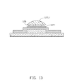
- a source electrode 128 and a drain electrode 129 are respectively formed at two symmetric sides of the gate electrode 120 . Both of the source electrode 128 and the drain electrode 129 orderly cover the etch stop pattern 126 , the semiconductor pattern 124 , and the gate insulator 122 .
Landscapes
- Engineering & Computer Science (AREA)
- Power Engineering (AREA)
- Microelectronics & Electronic Packaging (AREA)
- Physics & Mathematics (AREA)
- Condensed Matter Physics & Semiconductors (AREA)
- General Physics & Mathematics (AREA)
- Computer Hardware Design (AREA)
- Ceramic Engineering (AREA)
- Manufacturing & Machinery (AREA)
- Thin Film Transistor (AREA)
- Chemical & Material Sciences (AREA)
- Crystallography & Structural Chemistry (AREA)
Abstract
Description
Claims (10)
Applications Claiming Priority (3)
| Application Number | Priority Date | Filing Date | Title |
|---|---|---|---|
| TW102126750A TWI511200B (en) | 2013-07-25 | 2013-07-25 | Manufacturing method of display panel |
| TW102126750A | 2013-07-25 | ||
| TW102126750 | 2013-07-25 |
Publications (2)
| Publication Number | Publication Date |
|---|---|
| US20150031168A1 US20150031168A1 (en) | 2015-01-29 |
| US9257565B2 true US9257565B2 (en) | 2016-02-09 |
Family
ID=52390838
Family Applications (1)
| Application Number | Title | Priority Date | Filing Date |
|---|---|---|---|
| US14/340,573 Active US9257565B2 (en) | 2013-07-25 | 2014-07-25 | Display panel and manufacturing method thereof |
Country Status (3)
| Country | Link |
|---|---|
| US (1) | US9257565B2 (en) |
| CN (1) | CN104347496B (en) |
| TW (1) | TWI511200B (en) |
Families Citing this family (4)
| Publication number | Priority date | Publication date | Assignee | Title |
|---|---|---|---|---|
| CN103715270B (en) * | 2013-12-31 | 2016-03-09 | 京东方科技集团股份有限公司 | Thin-film transistor and preparation method thereof, display device |
| CN106298951B (en) * | 2015-05-28 | 2019-12-17 | 鸿富锦精密工业(深圳)有限公司 | Method for manufacturing thin film transistor |
| TWI694521B (en) * | 2019-03-22 | 2020-05-21 | 友達光電股份有限公司 | Semiconductor structure and manufacturing method thereof |
| CN113161291B (en) * | 2021-04-08 | 2022-11-15 | 北海惠科光电技术有限公司 | Array substrate manufacturing method and array substrate |
Citations (17)
| Publication number | Priority date | Publication date | Assignee | Title |
|---|---|---|---|---|
| US5299041A (en) * | 1991-07-11 | 1994-03-29 | France Telecom Etablissement Autonome De Droit Public | Active matrix, high definition, liquid crystal display structure |
| US5441905A (en) * | 1993-04-29 | 1995-08-15 | Industrial Technology Research Institute | Process of making self-aligned amorphous-silicon thin film transistors |
| US5610082A (en) * | 1992-12-29 | 1997-03-11 | Lg Electronics Inc. | Method for fabricating thin film transistor using back light exposure |
| US5637519A (en) * | 1996-03-21 | 1997-06-10 | Industrial Technology Research Institute | Method of fabricating a lightly doped drain thin-film transistor |
| US5658805A (en) * | 1991-06-28 | 1997-08-19 | U.S. Philips Corporation | Method of fabricating thin-film transistors |
| US6022753A (en) * | 1998-05-11 | 2000-02-08 | Samsung Electronics Co., Ltd. | Manufacturing methods of liquid crystal displays |
| US6184069B1 (en) * | 1999-05-24 | 2001-02-06 | Chi Mei Electronics Corp. | Fabrication of thin film transistor-liquid crystal display with self-aligned transparent conducting layers |
| US6326129B1 (en) * | 1999-03-16 | 2001-12-04 | Matsushita Electric Industrial Co., Ltd. | Process for manufacturing an active element array substrate |
| US6778250B2 (en) * | 1999-05-25 | 2004-08-17 | Lg. Phillips Lcd Co., Ltd. | Liquid crystal display having aligned pixel electrodes and fabricating method thereof |
| TW200534017A (en) | 2004-04-06 | 2005-10-16 | Quanta Display Inc | Structure of LTPS-TFT and fabricating method thereof |
| US20080206914A1 (en) * | 2007-02-26 | 2008-08-28 | Michael Albert Haase | Patterning self-aligned transistors using back surface illumination |
| US20080224184A1 (en) * | 2004-01-24 | 2008-09-18 | Koninklijke Philips Electronic, N.V. | Transistor Manufacture |
| US20110042667A1 (en) * | 2009-08-21 | 2011-02-24 | Hitachi, Ltd. | Semiconductor device and method for manufacturing the same |
| US8094251B2 (en) * | 2006-04-07 | 2012-01-10 | Au Optronics Corp. | Method for manufacturing lower substrate of liquid crystal display device |
| US20130077012A1 (en) * | 2010-07-08 | 2013-03-28 | Kenshi Tada | Semiconductor device and method for manufacturing the same, and liquid crystal display device |
| TW201327002A (en) | 2011-12-23 | 2013-07-01 | Au Optronics Corp | Pixel structure and manufacturing method thereof |
| US20140011329A1 (en) * | 2011-01-18 | 2014-01-09 | Peking University Shenzhen Graduate School | Method for manufacturing self-aligned thin film transistor |
Family Cites Families (1)
| Publication number | Priority date | Publication date | Assignee | Title |
|---|---|---|---|---|
| US5597747A (en) * | 1995-12-15 | 1997-01-28 | Industrial Technology Research Institute | Method of making inverted thin film transistor using backsick exposure and negative photoresist |
-
2013
- 2013-07-25 TW TW102126750A patent/TWI511200B/en not_active IP Right Cessation
- 2013-07-30 CN CN201310323704.8A patent/CN104347496B/en not_active Expired - Fee Related
-
2014
- 2014-07-25 US US14/340,573 patent/US9257565B2/en active Active
Patent Citations (17)
| Publication number | Priority date | Publication date | Assignee | Title |
|---|---|---|---|---|
| US5658805A (en) * | 1991-06-28 | 1997-08-19 | U.S. Philips Corporation | Method of fabricating thin-film transistors |
| US5299041A (en) * | 1991-07-11 | 1994-03-29 | France Telecom Etablissement Autonome De Droit Public | Active matrix, high definition, liquid crystal display structure |
| US5610082A (en) * | 1992-12-29 | 1997-03-11 | Lg Electronics Inc. | Method for fabricating thin film transistor using back light exposure |
| US5441905A (en) * | 1993-04-29 | 1995-08-15 | Industrial Technology Research Institute | Process of making self-aligned amorphous-silicon thin film transistors |
| US5637519A (en) * | 1996-03-21 | 1997-06-10 | Industrial Technology Research Institute | Method of fabricating a lightly doped drain thin-film transistor |
| US6022753A (en) * | 1998-05-11 | 2000-02-08 | Samsung Electronics Co., Ltd. | Manufacturing methods of liquid crystal displays |
| US6326129B1 (en) * | 1999-03-16 | 2001-12-04 | Matsushita Electric Industrial Co., Ltd. | Process for manufacturing an active element array substrate |
| US6184069B1 (en) * | 1999-05-24 | 2001-02-06 | Chi Mei Electronics Corp. | Fabrication of thin film transistor-liquid crystal display with self-aligned transparent conducting layers |
| US6778250B2 (en) * | 1999-05-25 | 2004-08-17 | Lg. Phillips Lcd Co., Ltd. | Liquid crystal display having aligned pixel electrodes and fabricating method thereof |
| US20080224184A1 (en) * | 2004-01-24 | 2008-09-18 | Koninklijke Philips Electronic, N.V. | Transistor Manufacture |
| TW200534017A (en) | 2004-04-06 | 2005-10-16 | Quanta Display Inc | Structure of LTPS-TFT and fabricating method thereof |
| US8094251B2 (en) * | 2006-04-07 | 2012-01-10 | Au Optronics Corp. | Method for manufacturing lower substrate of liquid crystal display device |
| US20080206914A1 (en) * | 2007-02-26 | 2008-08-28 | Michael Albert Haase | Patterning self-aligned transistors using back surface illumination |
| US20110042667A1 (en) * | 2009-08-21 | 2011-02-24 | Hitachi, Ltd. | Semiconductor device and method for manufacturing the same |
| US20130077012A1 (en) * | 2010-07-08 | 2013-03-28 | Kenshi Tada | Semiconductor device and method for manufacturing the same, and liquid crystal display device |
| US20140011329A1 (en) * | 2011-01-18 | 2014-01-09 | Peking University Shenzhen Graduate School | Method for manufacturing self-aligned thin film transistor |
| TW201327002A (en) | 2011-12-23 | 2013-07-01 | Au Optronics Corp | Pixel structure and manufacturing method thereof |
Also Published As
| Publication number | Publication date |
|---|---|
| US20150031168A1 (en) | 2015-01-29 |
| TW201505093A (en) | 2015-02-01 |
| CN104347496B (en) | 2017-02-15 |
| CN104347496A (en) | 2015-02-11 |
| TWI511200B (en) | 2015-12-01 |
Similar Documents
| Publication | Publication Date | Title |
|---|---|---|
| US10539836B2 (en) | Display substrate, method of fabricating the same, and display device | |
| US9711542B2 (en) | Method for fabricating display panel | |
| US9379148B2 (en) | Array substrate and method of manufacturing the same, and display device | |
| KR102248645B1 (en) | Thin Film Transistor Substrate Having Metal Oxide Semiconductor and Manufacturing Method Thereof | |
| US10268082B2 (en) | Display panel and method of manufacturing the same, and display device | |
| US20150333182A1 (en) | Method of fabricating array substrate, array substrate, and display device | |
| CN106200090B (en) | Display panel and method for manufacturing the same | |
| US8962404B2 (en) | Method for manufacturing fan-out lines on array substrate | |
| US8502945B2 (en) | Array substrate of fringe field switching mode liquid crystal display panel and method of manufacturing the same | |
| US9257565B2 (en) | Display panel and manufacturing method thereof | |
| US20170255044A1 (en) | Tft substrates and the manufacturing methods thereof | |
| US10985190B2 (en) | Active device substrate and fabricating method thereof | |
| US20170205662A1 (en) | Array substrate, manufacturing method thereof, and display apparatus | |
| WO2015180357A1 (en) | Array substrate and manufacturing method therefor, and display device | |
| US8537327B2 (en) | Array substrate and manufacturing method thereof, liquid crystal display | |
| US9837449B2 (en) | Display device with contact between an electrode of a thin film transistor and a pixel electrode | |
| KR102196335B1 (en) | Display device and method of fabricating the same | |
| US9081243B2 (en) | TFT substrate, method for producing same, and display device | |
| US8541268B2 (en) | Method for manufacturing thin film transistor | |
| US9076691B2 (en) | Thin film transistor array panel and method of manufacturing the same | |
| US9383608B2 (en) | Array substrate and manufacturing method thereof | |
| US20190206907A1 (en) | Array substrate and manufacturing method thereof | |
| US9035364B2 (en) | Active device and fabricating method thereof | |
| US20160027904A1 (en) | Method for manufacturing coplanar oxide semiconductor tft substrate | |
| TWI569456B (en) | Thin film transistor and manufacturing method thereof |
Legal Events
| Date | Code | Title | Description |
|---|---|---|---|
| AS | Assignment |
Owner name: YE XIN TECHNOLOGY CONSULTING CO., LTD., TAIWAN Free format text: ASSIGNMENT OF ASSIGNORS INTEREST;ASSIGNOR:SHIH, PO-LI;REEL/FRAME:033388/0641 Effective date: 20140724 |
|
| STCF | Information on status: patent grant |
Free format text: PATENTED CASE |
|
| AS | Assignment |
Owner name: HON HAI PRECISION INDUSTRY CO., LTD., TAIWAN Free format text: ASSIGNMENT OF ASSIGNORS INTEREST;ASSIGNOR:YE XIN TECHNOLOGY CONSULTING CO., LTD.;REEL/FRAME:038929/0856 Effective date: 20160308 |
|
| MAFP | Maintenance fee payment |
Free format text: PAYMENT OF MAINTENANCE FEE, 4TH YEAR, LARGE ENTITY (ORIGINAL EVENT CODE: M1551); ENTITY STATUS OF PATENT OWNER: LARGE ENTITY Year of fee payment: 4 |
|
| MAFP | Maintenance fee payment |
Free format text: PAYMENT OF MAINTENANCE FEE, 8TH YEAR, LARGE ENTITY (ORIGINAL EVENT CODE: M1552); ENTITY STATUS OF PATENT OWNER: LARGE ENTITY Year of fee payment: 8 |