US9257547B2 - III-N device structures having a non-insulating substrate - Google Patents
III-N device structures having a non-insulating substrate Download PDFInfo
- Publication number
- US9257547B2 US9257547B2 US13/231,308 US201113231308A US9257547B2 US 9257547 B2 US9257547 B2 US 9257547B2 US 201113231308 A US201113231308 A US 201113231308A US 9257547 B2 US9257547 B2 US 9257547B2
- Authority
- US
- United States
- Prior art keywords
- iii
- layer
- material layer
- silicon substrate
- barrier layer
- Prior art date
- Legal status (The legal status is an assumption and is not a legal conclusion. Google has not performed a legal analysis and makes no representation as to the accuracy of the status listed.)
- Active, expires
Links
- 239000000758 substrate Substances 0.000 title claims abstract description 182
- 239000000463 material Substances 0.000 claims abstract description 174
- 230000004888 barrier function Effects 0.000 claims abstract description 97
- XUIMIQQOPSSXEZ-UHFFFAOYSA-N Silicon Chemical compound [Si] XUIMIQQOPSSXEZ-UHFFFAOYSA-N 0.000 claims description 53
- 229910052710 silicon Inorganic materials 0.000 claims description 53
- 239000010703 silicon Substances 0.000 claims description 53
- 230000006911 nucleation Effects 0.000 claims description 16
- 238000010899 nucleation Methods 0.000 claims description 16
- 229910010293 ceramic material Inorganic materials 0.000 claims description 5
- 239000004020 conductor Substances 0.000 claims description 5
- 239000012777 electrically insulating material Substances 0.000 claims description 3
- 238000000034 method Methods 0.000 description 17
- 239000004065 semiconductor Substances 0.000 description 14
- JMASRVWKEDWRBT-UHFFFAOYSA-N Gallium nitride Chemical compound [Ga]#N JMASRVWKEDWRBT-UHFFFAOYSA-N 0.000 description 11
- HBMJWWWQQXIZIP-UHFFFAOYSA-N silicon carbide Chemical compound [Si+]#[C-] HBMJWWWQQXIZIP-UHFFFAOYSA-N 0.000 description 11
- 229910002601 GaN Inorganic materials 0.000 description 10
- 239000000203 mixture Substances 0.000 description 8
- 229910010271 silicon carbide Inorganic materials 0.000 description 8
- 230000008569 process Effects 0.000 description 7
- 238000000151 deposition Methods 0.000 description 5
- 230000008021 deposition Effects 0.000 description 5
- 230000015572 biosynthetic process Effects 0.000 description 4
- 230000015556 catabolic process Effects 0.000 description 4
- 239000002019 doping agent Substances 0.000 description 4
- 238000009877 rendering Methods 0.000 description 4
- 229910002704 AlGaN Inorganic materials 0.000 description 3
- 238000005336 cracking Methods 0.000 description 3
- 230000007547 defect Effects 0.000 description 3
- 230000010354 integration Effects 0.000 description 3
- 230000000903 blocking effect Effects 0.000 description 2
- 230000008878 coupling Effects 0.000 description 2
- 238000010168 coupling process Methods 0.000 description 2
- 238000005859 coupling reaction Methods 0.000 description 2
- 230000007423 decrease Effects 0.000 description 2
- 230000003247 decreasing effect Effects 0.000 description 2
- 238000010586 diagram Methods 0.000 description 2
- 230000000694 effects Effects 0.000 description 2
- 238000007667 floating Methods 0.000 description 2
- 239000011810 insulating material Substances 0.000 description 2
- 230000004048 modification Effects 0.000 description 2
- 238000012986 modification Methods 0.000 description 2
- TWNQGVIAIRXVLR-UHFFFAOYSA-N oxo(oxoalumanyloxy)alumane Chemical compound O=[Al]O[Al]=O TWNQGVIAIRXVLR-UHFFFAOYSA-N 0.000 description 2
- -1 Al2O3 Chemical compound 0.000 description 1
- PZNSFCLAULLKQX-UHFFFAOYSA-N Boron nitride Chemical compound N#B PZNSFCLAULLKQX-UHFFFAOYSA-N 0.000 description 1
- 208000032750 Device leakage Diseases 0.000 description 1
- 229910052581 Si3N4 Inorganic materials 0.000 description 1
- XLOMVQKBTHCTTD-UHFFFAOYSA-N Zinc monoxide Chemical compound [Zn]=O XLOMVQKBTHCTTD-UHFFFAOYSA-N 0.000 description 1
- 239000000956 alloy Substances 0.000 description 1
- 229910045601 alloy Inorganic materials 0.000 description 1
- 229910052782 aluminium Inorganic materials 0.000 description 1
- 230000009286 beneficial effect Effects 0.000 description 1
- 150000001875 compounds Chemical class 0.000 description 1
- 238000001816 cooling Methods 0.000 description 1
- PMHQVHHXPFUNSP-UHFFFAOYSA-M copper(1+);methylsulfanylmethane;bromide Chemical compound Br[Cu].CSC PMHQVHHXPFUNSP-UHFFFAOYSA-M 0.000 description 1
- 238000005516 engineering process Methods 0.000 description 1
- 230000002349 favourable effect Effects 0.000 description 1
- 230000006870 function Effects 0.000 description 1
- 229910052733 gallium Inorganic materials 0.000 description 1
- 238000001534 heteroepitaxy Methods 0.000 description 1
- 238000002513 implantation Methods 0.000 description 1
- 230000008676 import Effects 0.000 description 1
- 230000006872 improvement Effects 0.000 description 1
- 238000010348 incorporation Methods 0.000 description 1
- 229910052738 indium Inorganic materials 0.000 description 1
- 150000004767 nitrides Chemical class 0.000 description 1
- 239000012811 non-conductive material Substances 0.000 description 1
- 230000009467 reduction Effects 0.000 description 1
- HQVNEWCFYHHQES-UHFFFAOYSA-N silicon nitride Chemical compound N12[Si]34N5[Si]62N3[Si]51N64 HQVNEWCFYHHQES-UHFFFAOYSA-N 0.000 description 1
- 239000000126 substance Substances 0.000 description 1
- 230000005533 two-dimensional electron gas Effects 0.000 description 1
Images


Classifications
-
- H—ELECTRICITY
- H01—ELECTRIC ELEMENTS
- H01L—SEMICONDUCTOR DEVICES NOT COVERED BY CLASS H10
- H01L29/00—Semiconductor devices adapted for rectifying, amplifying, oscillating or switching, or capacitors or resistors with at least one potential-jump barrier or surface barrier, e.g. PN junction depletion layer or carrier concentration layer; Details of semiconductor bodies or of electrodes thereof ; Multistep manufacturing processes therefor
- H01L29/66—Types of semiconductor device ; Multistep manufacturing processes therefor
- H01L29/68—Types of semiconductor device ; Multistep manufacturing processes therefor controllable by only the electric current supplied, or only the electric potential applied, to an electrode which does not carry the current to be rectified, amplified or switched
- H01L29/76—Unipolar devices, e.g. field effect transistors
- H01L29/772—Field effect transistors
- H01L29/778—Field effect transistors with two-dimensional charge carrier gas channel, e.g. HEMT ; with two-dimensional charge-carrier layer formed at a heterojunction interface
- H01L29/7786—Field effect transistors with two-dimensional charge carrier gas channel, e.g. HEMT ; with two-dimensional charge-carrier layer formed at a heterojunction interface with direct single heterostructure, i.e. with wide bandgap layer formed on top of active layer, e.g. direct single heterostructure MIS-like HEMT
- H01L29/7787—Field effect transistors with two-dimensional charge carrier gas channel, e.g. HEMT ; with two-dimensional charge-carrier layer formed at a heterojunction interface with direct single heterostructure, i.e. with wide bandgap layer formed on top of active layer, e.g. direct single heterostructure MIS-like HEMT with wide bandgap charge-carrier supplying layer, e.g. direct single heterostructure MODFET
-
- H—ELECTRICITY
- H01—ELECTRIC ELEMENTS
- H01L—SEMICONDUCTOR DEVICES NOT COVERED BY CLASS H10
- H01L29/00—Semiconductor devices adapted for rectifying, amplifying, oscillating or switching, or capacitors or resistors with at least one potential-jump barrier or surface barrier, e.g. PN junction depletion layer or carrier concentration layer; Details of semiconductor bodies or of electrodes thereof ; Multistep manufacturing processes therefor
- H01L29/66—Types of semiconductor device ; Multistep manufacturing processes therefor
- H01L29/66007—Multistep manufacturing processes
- H01L29/66075—Multistep manufacturing processes of devices having semiconductor bodies comprising group 14 or group 13/15 materials
- H01L29/66227—Multistep manufacturing processes of devices having semiconductor bodies comprising group 14 or group 13/15 materials the devices being controllable only by the electric current supplied or the electric potential applied, to an electrode which does not carry the current to be rectified, amplified or switched, e.g. three-terminal devices
- H01L29/66409—Unipolar field-effect transistors
- H01L29/66446—Unipolar field-effect transistors with an active layer made of a group 13/15 material, e.g. group 13/15 velocity modulation transistor [VMT], group 13/15 negative resistance FET [NERFET]
- H01L29/66462—Unipolar field-effect transistors with an active layer made of a group 13/15 material, e.g. group 13/15 velocity modulation transistor [VMT], group 13/15 negative resistance FET [NERFET] with a heterojunction interface channel or gate, e.g. HFET, HIGFET, SISFET, HJFET, HEMT
-
- H—ELECTRICITY
- H01—ELECTRIC ELEMENTS
- H01L—SEMICONDUCTOR DEVICES NOT COVERED BY CLASS H10
- H01L2224/00—Indexing scheme for arrangements for connecting or disconnecting semiconductor or solid-state bodies and methods related thereto as covered by H01L24/00
- H01L2224/01—Means for bonding being attached to, or being formed on, the surface to be connected, e.g. chip-to-package, die-attach, "first-level" interconnects; Manufacturing methods related thereto
- H01L2224/42—Wire connectors; Manufacturing methods related thereto
- H01L2224/47—Structure, shape, material or disposition of the wire connectors after the connecting process
- H01L2224/48—Structure, shape, material or disposition of the wire connectors after the connecting process of an individual wire connector
- H01L2224/4805—Shape
- H01L2224/4809—Loop shape
- H01L2224/48091—Arched
-
- H—ELECTRICITY
- H01—ELECTRIC ELEMENTS
- H01L—SEMICONDUCTOR DEVICES NOT COVERED BY CLASS H10
- H01L2224/00—Indexing scheme for arrangements for connecting or disconnecting semiconductor or solid-state bodies and methods related thereto as covered by H01L24/00
- H01L2224/73—Means for bonding being of different types provided for in two or more of groups H01L2224/10, H01L2224/18, H01L2224/26, H01L2224/34, H01L2224/42, H01L2224/50, H01L2224/63, H01L2224/71
- H01L2224/732—Location after the connecting process
- H01L2224/73251—Location after the connecting process on different surfaces
- H01L2224/73265—Layer and wire connectors
-
- H—ELECTRICITY
- H01—ELECTRIC ELEMENTS
- H01L—SEMICONDUCTOR DEVICES NOT COVERED BY CLASS H10
- H01L29/00—Semiconductor devices adapted for rectifying, amplifying, oscillating or switching, or capacitors or resistors with at least one potential-jump barrier or surface barrier, e.g. PN junction depletion layer or carrier concentration layer; Details of semiconductor bodies or of electrodes thereof ; Multistep manufacturing processes therefor
- H01L29/02—Semiconductor bodies ; Multistep manufacturing processes therefor
- H01L29/12—Semiconductor bodies ; Multistep manufacturing processes therefor characterised by the materials of which they are formed
- H01L29/20—Semiconductor bodies ; Multistep manufacturing processes therefor characterised by the materials of which they are formed including, apart from doping materials or other impurities, only AIIIBV compounds
- H01L29/2003—Nitride compounds
-
- H—ELECTRICITY
- H01—ELECTRIC ELEMENTS
- H01L—SEMICONDUCTOR DEVICES NOT COVERED BY CLASS H10
- H01L2924/00—Indexing scheme for arrangements or methods for connecting or disconnecting semiconductor or solid-state bodies as covered by H01L24/00
- H01L2924/0001—Technical content checked by a classifier
- H01L2924/00014—Technical content checked by a classifier the subject-matter covered by the group, the symbol of which is combined with the symbol of this group, being disclosed without further technical details
Definitions
- the disclosed technology relates to semiconductor electronic devices, and specifically to nitride-based devices grown on non-insulating substrates.
- III-N films such as GaN and its alloys
- the films are grown on sapphire (Al 2 O 3 ), silicon carbide (SiC), or silicon substrates.
- Silicon substrates are emerging as a particularly attractive substrate candidate for III-N layers due to their low cost, wide availability, large wafer sizes, thermal properties, and ease of integration with silicon-based electronics.
- III-N layers on silicon substrates that are crack-free and that exhibit adequate structural quality can be difficult to achieve.
- the maximum thickness of III-N layers that can be grown without sustaining substantial defects may be limited. If the III-N layers are grown too thick, tensile stress in the layer becomes substantial, which can cause cracking upon cooling. In many applications in which III-N heteroepitaxial layers are used, it may be necessary that substantially thick III-N layers of adequate quality be grown on the foreign substrates.
- a III-N device in one aspect, includes a first material layer having a first side and a second side opposite the first side, and a first III-N material layer on the first side of the first material layer, the first III-N material layer including a channel layer.
- the III-N device further includes a second III-N material layer on the first III-N material layer, and a barrier layer disposed on the second side of the first material layer. The barrier layer is less electrically conductive than the first material layer.
- a III-N device in another aspect, includes a substrate layer having a first side and a second side opposite the first side, and a III-N material layer on the first side of the substrate layer, the substrate layer being electrically non-insulating.
- the III-N device further includes a diode structure in contact with the second side of the substrate layer, and a conductive portion of a device package in contact with a side of the diode structure opposite the substrate layer. The conductive portion of the device package is configured to be connected to ground.
- a III-N device in yet another aspect, includes a substrate layer having a first side and a second side opposite the first side, a first III-N material layer on the first side of the substrate layer, the first III-N material layer including a channel layer, and a second III-N material layer on the first III-N material layer.
- the substrate layer includes or is formed as a diode structure, the diode structure having a polarity to prevent current conduction through the substrate layer from the first side to the second side of the substrate layer.
- III-N devices described herein can include one or more of the following.
- the device can further comprise an electrically conductive layer on a side of the barrier layer opposite the first material layer.
- the electrically conductive layer can be a portion of a device package.
- the electrically conductive layer can be configured to be grounded or connected to a ground.
- the barrier layer can be configured to reduce, relative to a device lacking the barrier layer, a leakage current from the channel layer to the electrically conductive layer during device operation.
- the first material layer can be a conductive or partially conductive substrate.
- the substrate can include a material selected from the group consisting of silicon, silicon carbide (SiC), and gallium nitride (GaN).
- the first material layer can be a conductive or partially conductive carrier wafer.
- the device can further include a nucleation layer formed on the first material layer and a stress management layer formed on the nucleation layer, where the first III-N material layer is formed on the stress management layer.
- the barrier layer can be bonded to the first material layer.
- the channel layer can include a conductive channel.
- the barrier layer can include or be formed of high electrical resistivity material.
- the barrier layer can include or be formed of electrically insulating material.
- the barrier layer can include or be formed of thermally conductive material.
- the barrier layer can include or be formed of AlN or a ceramic material.
- a compositional difference between the first III-N material layer and the second III-N material layer can induce a 2DEG channel in the first III-N material layer.
- the device can further include a source contact, a drain contact, and a gate, the gate being adjacent to the second III-N material layer, and the source contact and drain contact being in electrical contact with the 2DEG, with the device being an enhancement mode FET.
- the device can further include a source contact, a drain contact and a gate, the gate being in contact with the second III-N material layer, and the source contact and drain contact being in electrical contact with the 2DEG, with the device being a depletion mode FET.
- the device can further include a source contact, a drain contact, and a gate, with the source and drain contacts and gate being over a side of the second III-N material layer opposite the first III-N material layer.
- the device can further include an anode contacting at least one of the first and second III-N material layers and a cathode contacting the 2DEG channel, the device being a diode.
- the diode structure can be configured to substantially prevent device leakage current from flowing through the substrate layer from the first side to the second side.
- the substrate layer can include or be formed of a material selected from the group consisting of silicon, SiC, and GaN.
- a first portion of the diode structure proximate to the substrate layer can be of a first conductivity type, and a second portion of the diode structure distal from the substrate layer can be of a second conductivity type.
- the first conductivity type can be n-type
- the second conductivity type can be p-type.
- the III-N material layer can include a first III-N material layer and a second III-N material layer adjacent to the first III-N material layer, where a compositional difference between the first III-N material layer and the second III-N material layer induces a 2DEG channel in the first III-N material layer.
- the device can further include a source contact, a drain contact, and a gate, the source and drain contacts and the gate being over a side of the III-N material layer opposite the substrate layer.
- a first portion of the diode structure adjacent to the first side can be of a first conductivity type, and a second portion of the diode structure adjacent to the second side can be of a second conductivity type.
- the first conductivity type can be n-type, and the second conductivity type can be p-type.
- the diode structure can be configured to be reverse biased during device operation.
- the device can further include a source contact, a drain contact, and a gate, the source and drain contacts and gate being over a side of the second III-N material layer opposite the substrate layer.
- a compositional difference between the first III-N material layer and the second III-N material layer can induce a 2DEG channel in the first III-N material layer.
- the device can further include a nucleation layer formed on the substrate layer.
- the device can further include a stress management layer disposed on the nucleation layer, where the first III-N material layer is formed on the stress management layer.
- a method of forming or producing a III-N device includes forming a first III-N material layer and a second III-N material layer, the first III-N material layer including a channel layer.
- the first and second III-N material layers are over a first side of a first material layer, the first III-N material layer being between the second III-N material layer and the first material layer.
- the method further includes forming a barrier layer on a second side of the first material layer, the second side of the first material layer being opposite the first side of the first material layer.
- the barrier layer can be less electrically conductive than the first material layer.
- Methods of forming or producing a III-N device can include one or more of the following.
- the first material layer can be a substrate, and forming the first and second III-N material layers can include forming the first and second III-N material layers over the first side of the first material layer by epitaxial growth or deposition. Forming the first and second III-N material layers can include forming the first and second III-N material layers on a substrate, removing the substrate from the first and second III-N material layers, and joining the first and second III-N material layers to the first side of the first material layer.
- the first material layer can be a carrier wafer.
- the method can further include forming a nucleation layer on the first side of the first material layer and forming a stress management layer on the nucleation layer, whereby the first III-N material layer is joined to the stress management layer.
- the device can be encapsulated in a package that surrounds the device, including joining the barrier layer to an electrically conductive package base of the package.
- the method can further include adding a gate over the first or second III-N material layer and adding source and drain electrodes on opposite sides of the gate.
- the method can further include adding a cathode contacting the channel layer of the first III-N material layer and adding an anode contacting the first or second III-N material layer.
- Devices and methods described herein can reduce leakage currents in semiconductor power devices, as well as increasing breakdown voltages in such devices.
- FIG. 1 is a cross-sectional view of an example of a III-N high electron mobility transistor (HEMT) device.
- HEMT high electron mobility transistor
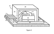
- FIG. 2 is a perspective cross-sectional view of a packaged semiconductor transistor.
- FIG. 3 is a representative circuit schematic illustrating the effective resistances in the device of FIG. 2 during off-state operation when the package base is left floating.
- FIG. 4 is a representative circuit schematic illustrating the effective resistances in the device of FIG. 2 during off-state operation when the package base is grounded.
- FIG. 5 is a cross-sectional view of an example of another III-N HEMT device.
- FIG. 6 is a perspective cross-sectional view of the HEMT of FIG. 5 encased in a package.
- FIG. 7 is a representative circuit schematic showing the contribution to the overall resistance seen at the drain of the device of FIG. 6 during times where the gate of the device is biased off and the device blocks a high voltage.
- FIGS. 8 and 9 are cross-sectional views of example III-N high electron mobility transistor (HEMT) devices.
- HEMT high electron mobility transistor
- FIG. 10 is a representative circuit schematic showing equivalent discrete elements corresponding to various layers of the HEMT device of FIG. 8 .
- FIG. 11 is a representative circuit schematic showing equivalent discrete elements corresponding to various layers of the HEMT device of FIG. 9 .
- FIG. 12 illustrates an example III-N diode structure utilizing a barrier layer.
- FIG. 13 is a flow diagram of an example process 1300 for producing a III-N device.
- Embodiments of the present disclosure include structures and configurations for III-N devices or semiconductor devices having a conductive, partially conductive, semi-conductive, or otherwise non-insulating substrate.
- III-N devices that involve the heteroepitaxial growth or deposition of III-N layers on foreign substrates (i.e., substrates that differ substantially in composition and/or lattice structure from that of the deposited layers), such as silicon (Si), silicon carbide (SiC), or sapphire (Al 2 O 3 ), can require thick III-N layers.
- III-N electronic devices grown or deposited on conductive native substrates, such as n-type GaN or AlGaN can in many cases also require thick III-N layers grown atop the substrate. It can be difficult and/or expensive, however, to grow such thick III-N layers.
- the mismatch of lattice constants and thermal expansion coefficients, as well as chemical and structural properties, between the substrate and the III-N epitaxial layers can cause substantial stress in the layers during growth, causing the III-N layers to be in a strained state during growth.
- the mismatch of thermal coefficients of expansion between the III-N layers and the foreign substrates on which they are grown or deposited can cause further strain in the III-N layers as the layers are cooled from growth temperature, which is typically in the range of about 700° C.-1500° C., to room temperature.
- III-N devices grown on substrates there can be a trade-off between the device performance and other characteristics, such as cost and scalability, for various substrates.
- silicon or silicon-based substrates are emerging as an attractive substrate selection for III-N devices due to the low cost, wide availability, large wafer sizes, thermal and electrical properties, and ease of integration with silicon-based electronics.
- III-N layers grown on silicon substrates the stress in the III-N layers becomes more tensile (and/or less compressive) as the deposited layers are cooled from growth temperature to room temperature. If the amount of stress in the film becomes too large, strain relief can occur by formation of dislocations and stacking faults, cracks in the layer, or other defects that relax the lattice strain and stabilize the layer.
- III-N devices grown on conductive or non-insulating substrates, such as silicon or n-type silicon carbide substrates can be prone to inferior device properties, such as higher off-state leakage currents and lower breakdown voltage, as compared to devices grown on insulating or semi-insulating substrates, making them less favorable for high voltage applications.
- III-N devices grown on insulating or semi-insulating substrates typically have lower sub-surface leakage currents as compared to devices grown on more conductive substrates.
- silicon carbide based III-N devices are typically disadvantageous with respect to cost and scaling.
- III-Nitride or III-N materials, layers or devices refer to a material or device comprised of a compound semiconductor material according to the stoichiometric formula Al x In y Ga z N, where x+y+z is about 1.
- x, y, and z are compositions of Al, In and Ga, respectively.
- a “substrate” is a semiconductor material layer on top of which additional semiconductor material layers of a semiconductor device are deposited, for example, epitaxially grown, such that the crystalline structure of the grown semiconductor material contacting or adjacent to the substrate at least partially conforms to, or is at least partially determined by the crystalline structure of the substrate.
- a “semi-insulating substrate” can include a substrate with a substantially high resistivity such that there is substantially low conduction of current through the semi-insulating substrate.
- FIG. 1 shows a cross-sectional view of an example of a III-N high electron mobility transistor (HEMT) fabricated on substrate 10 .
- the III-N HEMT structure includes a substrate 10 , which can be a native or a foreign substrate, a nucleation layer 9 formed on the substrate 10 , such as AlN or Al x Ga 1-x N, and a buffer layer 8 disposed on the nucleation layer 9 .
- the nucleation layer 9 can be used to control the stress during material growth and in particular, for growth of thicker layers. In some instances, a stress management layer may also be disposed over the nucleation layer for additional stress control.
- the device structure further includes a channel layer 11 , disposed over the buffer layer 8 , and a barrier layer 12 , such as a layer of Al x Ga 1-x N, formed over the channel layer 11 .
- a two-dimensional electron gas (2DEG) channel 19 (illustrated by a dotted line) can be induced in the channel layer 11 near the interface between the channel layer 11 and the barrier layer 12 .
- Buffer layer 8 can include a single composition III-N material which in some cases has a higher energy bandgap than that of channel layer 11 . Therefore there can be an abrupt composition variation between the buffer layer 8 and the channel layer 11 .
- buffer layer 8 can include AlN or Al y Ga 1-y N, and the channel layer 11 can be GaN.
- the buffer layer 8 can be graded.
- layer 8 can include Al x Ga 1-x N with x ⁇ 1, such that the buffer layer 8 includes a continuous grade in composition (i.e., x varies continuously throughout the layer).
- the composition of buffer layer 8 is graded such that the energy bandgap is greatest at the interface with substrate 10 , and decreases to a minimum at the interface with the channel layer 11 .
- the effects of the tensile stress of the layer structure as it is cooled to room temperature, such as cracking or defect formation are mitigated by use of a graded buffer layer. Careful control of the growth or deposition conditions and thickness of buffer layer 8 is utilized to minimize the negative effects of the lattice and thermal mismatches between the channel layer 11 and substrate 10 .
- Source and drain electrodes 14 and 15 which are formed on opposite sides of the gate electrode 16 , contact the 2DEG channel 19 in channel layer 11 .
- Gate 16 modulates the portion of the 2DEG in the gate region, i.e., beneath gate 16 .
- III-N device The layer structure and choice of substrate on which a III-N device is grown can affect the performance of the device. It is desirable to provide III-N devices for which superior device performance, such as high off-state operating voltage, can be achieved while at the same time maintaining scalability, cost reduction, and easy integration with other circuit components.
- the transistor of FIG. 1 is a lateral device. That is, the source, gate, and drain electrodes are all on the same side of the device, for example on the top surface of the semiconductor material layers.
- the transistor of FIG. 1 can be a high voltage switching device, i.e., a high voltage switching transistor.
- a high voltage switching transistor is a transistor optimized for high voltage switching applications.
- the transistor when the transistor is off, it is capable of blocking high voltages, such as about 300V or higher, about 600V or higher, about 1200V or higher, or about 1700V or higher, and when the transistor is on, it has a sufficiently low on-resistance R ON for the application in which it is used, i.e., it experiences sufficiently low conduction loss when a substantial current passes through the device.
- the transistor of FIG. 1 when the transistor of FIG. 1 is configured to be used in a circuit, it can be encased, enclosed, or encapsulated in a package 19 which completely surrounds the transistor (i.e., the package can surround the transistor in three dimensions).
- the package 19 includes a case 24 , an electrically conductive package base 23 , also commonly referred to as a tab 23 , a source lead 70 , a gate lead 71 , and a drain lead 72 . Regions in the interior of the package 19 which are not occupied by the transistor are typically filled with an encapsulating material (not shown).
- the package base 23 is grounded or electrically connected to ground, such as by mounting the package 19 on a ground plane 27 with the package base 23 contacting the ground plane 27 .
- the ground plane 27 is an electrically conductive layer which is grounded or is electrically connected to ground.
- FIG. 3 is a representative circuit schematic illustrating the effective resistances in the device of FIG. 2 during off-state operation (i.e., operation at times where the gate 16 is biased below the threshold voltage of the device, rendering the device channel non-conductive) in applications where the package base 23 is not grounded, but is instead left floating (i.e., not electrically connected to any DC or AC voltage sources).
- the source electrode 14 is grounded, i.e., electrically connected to ground 33
- the drain electrode 15 is at a high voltage 34 , such that the device blocks a high voltage V 34 without substantial current flowing through the device channel 19 .
- any undesirable subsurface drain leakage current 36 passing through the substrate 10 flows approximately vertically from the drain electrode 15 into the substrate 10 , approximately horizontally through the substrate 10 , and approximately vertically from the substrate 10 to the source electrode 14 .
- the direction of current depicted in FIG. 3 is opposite the direction that electrons flow.
- the effective vertical resistance R 104 between the source electrode 14 and the substrate 10 , and between the drain electrode 15 and the substrate 10 is represented in FIG. 3 by resistors 104 .
- the effective lateral resistance R 100 through the substrate 10 is represented in FIG. 3 by resistor 100 .
- the magnitude of the subsurface drain leakage current 36 in FIG. 3 is inversely proportional to the effective source-drain resistance, or can be approximated by the source-drain voltage 34 divided by the effective source-drain resistance, or V 34 /(2*R 104 +R 100 ).
- the substrate 10 is non-conductive or insulating, (e.g., when R 100 is greater than or much larger than R 104 )
- the resulting subsurface drain leakage current 36 is small, and generally independent of the value of R 104 .
- the substrate is at least partially electrically conductive, electrically conductive, partially conductive, or otherwise non-insulating (for example if the substrate is silicon, n-type SiC, GaN, or another conductive substrate), such that R 100 is much smaller than R 104 , then the effective resistance between the source 14 and drain 15 is approximately 2*R 104 , and so layer 43 is designed to maximize or increase R 104 to decrease or minimize the subsurface drain leakage current 36 , which can be achieved by growing thicker III-N layers below the active device layers (i.e., III-N layers 11 and 12 ).
- the effective resistances in the device and resulting subsurface drain leakage current are about the same as those shown in FIG. 3 .
- substrate 10 is conductive or partially conductive, then the effective resistance seen by the drain is much lower, resulting in an increased subsurface drain leakage current, as further described below.
- FIG. 4 is a representative circuit schematic illustrating the effective resistances in the device of FIG. 2 during off-state operation (i.e., operation at times where the gate 16 is biased below the threshold voltage of the device, rendering the device channel non-conductive) in applications where the package base 23 is grounded.
- the resistor 104 below the source electrode 14 and the substrate resistor 100 are effectively shorted. Consequently, the effective resistance between the drain electrode 15 and the source electrode 14 , which is the same as the effective resistance between the drain electrode 15 and ground 33 , is approximately R 104 , which is approximately half the resistance seen by the drain in the case where a conductive substrate is used but the package base 23 is not grounded.
- the substrate 10 if conductive or non-insulating (e.g., silicon), can introduce a current leakage path through the substrate due to the decreased effective electrical impedance seen from the device drain.
- the decreased effective impedance results in increased leakage drain current through the substrate layer 10 thus negatively affecting the amount of voltage that can be applied during operation, as well as increasing off-state conduction losses.
- the device structure can be modified to increase the effective impedance seen at the device drain when an electrically conducting or semiconducting substrate is used.
- the effective impedance can be increased such that it is comparable to the effective impedance seen from the drain when the substrate is electrically conducting and the package base 23 is not grounded.
- the effective impedance can be increased by introducing insulating or less conductive material under the substrate 10 , for example between the substrate 10 and the package base 23 .
- the effective impedance can also be increased through use of a reverse biased device structure (e.g., reverse bias PN diode or PIN diode) in or below the substrate.
- One embodiment of the present disclosure is a III-N semiconductor device that includes a barrier layer beneath the substrate, i.e., on a side of the substrate opposite the device and channel layers.
- the material for the barrier layer can be selected to be electrically insulating or otherwise substantially non-conductive to electrical current.
- inclusion of a barrier layer can allow devices to be grown or deposited on an electrically conducting or semiconducting substrate, such as silicon, while simultaneously achieving ideal device properties for high-voltage applications, such as high breakdown voltage and low off-state leakage current, without the need to increase the thickness of the III-N layers in the device structure.
- An example of one embodiment of an III-N device utilizing a barrier layer to enhance or improve device characteristics by increasing the effective impedance is illustrated in FIG. 5 .
- FIG. 5 is a cross-sectional view of an example of a III-N HEMT device having a barrier layer 50 under a non-insulating layer 20 .
- Non-insulating layer 20 can be a non-insulating substrate on top of which III-N layers are epitaxially grown or deposited.
- non-insulating layer 20 can for example be a carrier wafer. That is, the III-N layers of the HEMT device can be grown on a substrate, the substrate is then removed, and a non-insulating carrier wafer can be attached or bonded to the surface exposed by the removal of the substrate.
- Layer 20 will herein be referred to as a substrate layer 20 , although as described above, other layers are possible as well.
- the III-N HEMT device of FIG. 5 can include a non-insulating substrate layer 20 , which can be a native or foreign substrate, a first III-N material layer 11 on one side of the substrate layer 20 , and a second III-N material layer 12 on the first III-N material layer 11 .
- the first III-N material layer 11 is or includes a channel layer.
- the device includes a barrier layer 50 disposed on another side of the substrate layer 20 (e.g., a side opposite of the first and second III-N material layers). As illustrated in FIG.
- the device when the III-N HEMT is encased, enclosed, or encapsulated in a package 19 , the device is mounted in the package 19 such that the barrier layer 50 is disposed between the substrate layer 20 and the electrically conductive package base 23 .
- the substrate layer 20 contacts one side of the barrier layer 50 and the package base 23 contacts an opposite side of the barrier layer.
- the barrier layer 50 is bonded to the substrate layer 20 .
- the barrier layer 50 is less electrically conductive than the substrate layer 20 , such that in applications where the package base 23 is grounded, the overall impedance seen at the drain of the device during times where the device is biased off (i.e., when the gate is biased relative to the source at a voltage which is less than the device threshold voltage) is increased by the addition of layer 50 .
- the substrate layer 20 may be electrically conductive or partially conductive.
- substrate 20 can include or be formed of silicon, doped AlN, SiC (e.g., n-type SiC), GaN, or any another electrically conductive native or foreign substrate suitable for use in III-N devices.
- FIG. 7 is a representative circuit schematic showing the contribution to the overall resistance seen at the drain of the device of FIG. 6 during times where the gate of the device is biased off and the device blocks a high voltage.
- the off-state drain leakage current in cases where the package base 23 is grounded is approximately half that of a device which lacks the barrier layer 50 but is otherwise identical.
- the barrier layer 50 can be of a material such that during device operation there is substantially no current flowing through it. That is, the material and thickness of the barrier layer 50 are chosen such that substantially no current (i.e., less than 0.001 times the average on-state current of the overlying transistor device) flows through the barrier layer 50 when a voltage less than or equal to the breakdown voltage of the overlying transistor is applied across the thickness of the barrier layer 50 .
- the minimum thickness of the barrier layer 50 depends on the particular material that is used, specifically on the number of volts that can be supported per micron of thickness of the material.
- the barrier layer 50 is at least 5 microns thick, such as between 10 microns and 300 microns thick. In other implementations, the barrier layer is at least 10 microns, at least 30 microns, or at least 100 microns thick.
- the barrier layer 50 can include high electrical resistivity material or material that is otherwise electrically insulating, including by way of example but not limitation, aluminum nitride, silicon nitride, a ceramic material, amorphous SiC, Al 2 O 3 , zinc oxide (ZnO), boron nitride (BN), or any other insulating or partially insulating material.
- the barrier layer 50 can be capable of transporting or conducting substantial heat or thermal energy.
- the ground plane 27 which the package base 23 is mounted on can also serve as a heat sink to collect the heat generated in the device during device operation. As such, the heat must conduct through barrier layer 50 .
- barrier layer can include a material that conducts heat well, or material that is thermally conductive.
- barrier layer 50 can be made thin to further enhance its total thermal conductance.
- the thermal conductivity of barrier layer 50 is sufficiently high and the thickness is sufficiently low to conduct sufficient heat generated in the device for the particular application in which the device is used.
- the thermal conductivity of barrier layer 50 can be greater than 1 (W/cm)/K, greater than 1.3 (W/cm)/K, or greater than 2 (W/cm)/K, and the thickness can be less than 300 microns, less than 100 microns, less than 50 microns, or less than 20 microns.
- the material of barrier layer 50 has a thermal conductivity which is greater than that of the substrate layer 20 .
- the thermal conductivity of the barrier layer 50 can be greater than 1.3 (W/cm)/K.
- the III-N layers 11 and 12 can have different compositions.
- the compositions can be chosen such that a 2DEG channel 19 (illustrated by a dotted line) is induced in the first III-N material layer 11 , which can also be referred to as “channel layer 11 ”.
- channel layer 11 a 2DEG channel 19 (illustrated by a dotted line) is induced in the first III-N material layer 11 , which can also be referred to as “channel layer 11 ”.
- some or all of the III-N material in layer 12 can have a bandgap which is larger than that of layer 11 , so layer 12 can also be referred to as “barrier layer 12 ”.
- the first III-N material layer 11 and the second III-N material layer 12 can be GaN and Al x Ga 1-x N, respectively, where x can be between 0 and 1 or equal to 1.
- the device includes a nucleation layer 9 , such as AlN, AlGaN, or AlInGaN, formed on the substrate layer 20 .
- the device can also include a stress management layer 8 disposed on the nucleation layer 9 , with the III-N material layers that form the basis for the HEMT device (e.g., the III-N layers 11 and 12 ) formed on the stress management layer 8 .
- the stress management layer 8 can include, for example, thin AlN layers, a graded or stepped Al x Ga 1-x N layer, and/or AlGaN/GaN or AlN/GaN superlattices.
- the device further includes a source contact 14 , a drain contact 15 and a gate 16 .
- the gate 16 can be adjacent to the second III-N material layer 12 and the source contact 14 and drain contact 15 are in electrical contact with the 2DEG 19 .
- the device can be a lateral device, as previously described.
- the device can be an enhancement mode FET or a depletion mode FET.
- Additional examples of typical III-N devices that can be fabricated on foreign substrates and utilizing a barrier layer 50 can include, by way of example but not limitation, High Electron Mobility Transistors (HEMTs), POLFETs, MESFETs, LEDs, Diode Lasers, and Current Aperture Vertical Electron Transistors (CAVETs).
- novel art of the disclosure includes any device or structure configuration which causes the effective drain impedance to increase and is not limited to the incorporation of a barrier layer comprised of non-conductive or insulating material.
- diode structures can be used as barriers to prevent drain leakage currents from flowing to ground directly through the substrate layer, examples of which are illustrated in FIGS. 8 and 9 .
- FIG. 8 is a cross-sectional view of a III-N transistor similar to that of FIG. 1 , except that the substrate layer or carrier wafer 80 (herein substrate layer 80 ) includes or is formed as a diode structure.
- region 81 can be an n-type semiconductor, such as n-type silicon
- region 82 can be a p-type semiconductor, such as p-type silicon, hence forming a p-n diode structure in the substrate 80 .
- the diode structure is formed in the substrate layer through implantation. That is, the substrate layer can be implanted with dopants from an opposite side of the first III-N material layer such that a diode structure is formed in the substrate layer.
- the reverse side i.e., the side opposite the III-N material layers
- an n-type substrate such as an n-type silicon substrate
- the p-type dopants can be implanted either before or after formation of the III-N material layers.
- a diode structure is formed in the substrate by implanting the side of the substrate upon which the III-N material layers are grown (i.e., the growth side of the substrate).
- the growth side of a p-type substrate such as a p-type silicon substrate, can be implanted with n-type dopants, rendering the growth side of the substrate n-type.
- the diode structure in the substrate is formed during formation of the substrate material layer(s).
- the substrate 80 in FIG. 8 can be formed by first forming a p-type region 82 and then forming an n-type region 81 on the p-type region 82 .
- One or both of the regions 81 and 82 can be formed by epitaxial growth.
- Region 81 that is the portion of the substrate adjacent to the III-N material layers, can be electrically conductive, partially conductive, or otherwise non-insulating.
- the diode in the substrate can include additional portions, for example a lightly doped or intrinsic region between n-type region 81 and p-type-region 82 , thereby forming a p-i-n diode structure in the substrate.
- FIG. 10 depicts a circuit schematic showing equivalent discrete elements corresponding to various layers of the HEMT device of FIG. 8 .
- the circuit schematic is again drawn for the case where the device is mounted on a grounded portion and the device is biased in the off state, such that it blocks a high voltage 34 .
- the diodes 115 are reversed biased, preventing subsurface drain leakage currents from flowing through the entire thickness of the substrate to ground 33 .
- the subsurface drain leakage current 36 flows from drain 15 to source 14 along the path shown, thereby resulting in a larger effective drain resistance and lower drain leakage currents than in a device lacking a barrier layer.
- the diode can be a power diode, a p-n diode, a p-i-n diode, or a p-i-n power diode, for example.
- a GaN HEMT can be grown on an n-i-p power diode based on silicon or other material systems.
- FIG. 9 is a cross-sectional view of a III-N transistor similar to that of FIG. 1 , but further including a diode structure 90 on an opposite side of the conductive substrate 20 from the III-N material layers 43 .
- Diode structure 90 can include an n-type region 91 and a p-type region 92 , or can be formed as any of the diode structures described for the substrate layer 80 of FIG. 8 .
- FIG. 11 depicts a circuit schematic showing equivalent discrete elements corresponding to various layers of the HEMT device of FIG. 9 . The circuit schematic is again drawn for the case where the device is mounted on a grounded portion and the device is biased in the off state, such that it blocks a high voltage 34 .
- the diodes 115 are reversed biased, preventing subsurface drain leakage currents from flowing through the entire thickness of the substrate to ground 33 .
- the subsurface drain leakage current 36 flows from drain 15 to source 14 along the path shown, thereby resulting in a larger effective drain resistance and lower drain leakage currents than in a device lacking a barrier layer.
- III-N diode structure utilizing a barrier layer is illustrated in FIG. 12 .
- the III-N diode in the example of FIG. 12 includes similar or the same material layers to those of the HEMT of FIG. 5 .
- the electrode structure is different.
- the diode of FIG. 12 includes an anode contact 6 which directly contacts at least one of the underlying III-N material layers.
- the anode contact 6 can form a Schottky contact to the III-N material layer or layers which it directly contacts.
- the diode also includes a single cathode contact 5 which contacts the device channel (i.e., 2DEG 19 ) and can form an ohmic contact to the device channel.
- the diode is forward biased and conducting current, the voltage of anode contact 6 is larger than that of cathode contact 5 .
- the diode is reverse biased and blocking a voltage, the voltage of cathode contact 5 is larger than that of anode contact 6 , and only a small reverse leakage current flows through the diode.
- barrier layer 50 prevents current from being able to flow from the anode contact 6 or the cathode contact 5 directly to ground through substrate layer 20 when the barrier layer 50 is mounted on a circuit ground, such as when the III-N diode is packaged and operated in a circuit.
- a sufficiently insulating barrier layer 50 is used, the off-state drain leakage current of the diode in applications where the barrier layer 50 is mounted on a circuit ground can be approximately half that of a diode which lacks the barrier layer 50 but is otherwise identical to that of FIG. 12 .
- FIG. 13 is a flow diagram of an example process 1300 for producing a III-N device, e.g., any of the devices described above.
- First and second III-N material layers are formed (e.g., layers 11 and 12 in FIG. 5 ), the second III-N material layer being above the first III-N material layer (step 1302 ).
- the first and second III-N material layers can be formed by epitaxial growth or deposition.
- the first and second III-N material layers can be formed on any of various appropriate structures.
- the first and second III-N material layers can be deposited on a substrate, on a non-insulating layer (e.g., layer 20 in FIG. 5 ), or on a diode structure (e.g., as layers 81 and 82 in FIG. 8 or layers 91 and 92 in FIG. 9 ).
- a nucleation layer and/or a stress management layer are formed on a structure (step 1304 ), and the first and second III-N material layers are formed on the nucleation layer or stress management layer.
- the substrate is subsequently removed after the deposition, and the first and second III-N material layers are joined to a carrier wafer (step 1306 ).
- the surface of the first and second III-N material layers that is exposed by removal of the substrate can be attached or bonded to the carrier wafer.
- a barrier layer (e.g., layer 50 in FIG. 5 ) may be formed on the opposite side of the non-insulating layer from the III-N material layers (step 1308 ).
- the barrier layer can be formed on the opposite side of the carrier wafer from the III-N material layers.
- Contacts are added to the device to make it a transistor (e.g., as shown in FIGS. 5 , 8 , and 9 ) or a diode (e.g., as shown in FIG. 12 ) (step 1310 ). If the device is a transistor, source and drain electrodes and a gate are added. If the device is a diode, an anode and a cathode are added.
- the device is encapsulated in a package (e.g., the package 19 of FIG. 6 ) that surrounds the device (step 1312 ).
- the device can be bonded to an electrically conductive package base.
- the package base can be grounded or electrically connected to ground.
- the package can be mounted on a ground plane with the package based contacting the ground plane.
- the words “comprise,” “comprising,” and the like are to be construed in an inclusive sense, as opposed to an exclusive or exhaustive sense; that is to say, in the sense of “including, but not limited to.”
- the terms “connected,” “coupled,” or any variant thereof means any connection or coupling, either direct or indirect, between two or more elements; the coupling of connection between the elements can be physical, logical, or a combination thereof.
Abstract
Description
R drain =R 104 +[R 104 *R 105/(2*R 104 +R 105)].
If
Claims (30)
Priority Applications (1)
| Application Number | Priority Date | Filing Date | Title |
|---|---|---|---|
| US13/231,308 US9257547B2 (en) | 2011-09-13 | 2011-09-13 | III-N device structures having a non-insulating substrate |
Applications Claiming Priority (1)
| Application Number | Priority Date | Filing Date | Title |
|---|---|---|---|
| US13/231,308 US9257547B2 (en) | 2011-09-13 | 2011-09-13 | III-N device structures having a non-insulating substrate |
Publications (2)
| Publication Number | Publication Date |
|---|---|
| US20130062621A1 US20130062621A1 (en) | 2013-03-14 |
| US9257547B2 true US9257547B2 (en) | 2016-02-09 |
Family
ID=47829025
Family Applications (1)
| Application Number | Title | Priority Date | Filing Date |
|---|---|---|---|
| US13/231,308 Active 2034-10-18 US9257547B2 (en) | 2011-09-13 | 2011-09-13 | III-N device structures having a non-insulating substrate |
Country Status (1)
| Country | Link |
|---|---|
| US (1) | US9257547B2 (en) |
Cited By (6)
| Publication number | Priority date | Publication date | Assignee | Title |
|---|---|---|---|---|
| US9842835B1 (en) | 2016-10-10 | 2017-12-12 | International Business Machines Corporation | High density nanosheet diodes |
| US10630285B1 (en) | 2017-11-21 | 2020-04-21 | Transphorm Technology, Inc. | Switching circuits having drain connected ferrite beads |
| US10756207B2 (en) | 2018-10-12 | 2020-08-25 | Transphorm Technology, Inc. | Lateral III-nitride devices including a vertical gate module |
| US11749656B2 (en) | 2020-06-16 | 2023-09-05 | Transphorm Technology, Inc. | Module configurations for integrated III-Nitride devices |
| US11810971B2 (en) | 2019-03-21 | 2023-11-07 | Transphorm Technology, Inc. | Integrated design for III-Nitride devices |
| US11973138B2 (en) | 2022-01-28 | 2024-04-30 | Transphorm Technology, Inc. | N-polar devices including a depleting layer with improved conductivity |
Families Citing this family (10)
| Publication number | Priority date | Publication date | Assignee | Title |
|---|---|---|---|---|
| WO2013096821A1 (en) * | 2011-12-21 | 2013-06-27 | Massachusetts Institute Of Technology | Aluminum nitride based semiconductor devices |
| EP3708699A1 (en) | 2013-02-15 | 2020-09-16 | AZUR SPACE Solar Power GmbH | P-d0ping of group-i i i-nitride buffer later structure on a heterosubstrate |
| JP2014220407A (en) * | 2013-05-09 | 2014-11-20 | ローム株式会社 | Nitride semiconductor element |
| JP6244769B2 (en) * | 2013-09-19 | 2017-12-13 | 富士通株式会社 | Semiconductor device and manufacturing method of semiconductor device |
| WO2016060337A1 (en) * | 2014-10-13 | 2016-04-21 | 한국과학기술원 | Field effect transistor manufacturing method |
| US9583607B2 (en) * | 2015-07-17 | 2017-02-28 | Mitsubishi Electric Research Laboratories, Inc. | Semiconductor device with multiple-functional barrier layer |
| CN105355555A (en) * | 2015-10-28 | 2016-02-24 | 中国科学院微电子研究所 | GaN-based enhanced power electronic device and preparation method thereof |
| US10734537B2 (en) * | 2017-11-08 | 2020-08-04 | Wisconsin Alumni Research Foundation | High performance, high electron mobility transistors with graphene hole extraction contacts |
| US10950598B2 (en) * | 2018-01-19 | 2021-03-16 | Macom Technology Solutions Holdings, Inc. | Heterolithic microwave integrated circuits including gallium-nitride devices formed on highly doped semiconductor |
| CN112750904B (en) | 2019-10-30 | 2024-01-02 | 联华电子股份有限公司 | Semiconductor element with stress relaxation layer |
Citations (185)
| Publication number | Priority date | Publication date | Assignee | Title |
|---|---|---|---|---|
| US4300091A (en) | 1980-07-11 | 1981-11-10 | Rca Corporation | Current regulating circuitry |
| US4645562A (en) | 1985-04-29 | 1987-02-24 | Hughes Aircraft Company | Double layer photoresist technique for side-wall profile control in plasma etching processes |
| US4728826A (en) | 1986-03-19 | 1988-03-01 | Siemens Aktiengesellschaft | MOSFET switch with inductive load |
| US4821093A (en) | 1986-08-18 | 1989-04-11 | The United States Of America As Represented By The Secretary Of The Army | Dual channel high electron mobility field effect transistor |
| US4914489A (en) | 1986-12-20 | 1990-04-03 | Fujitsu Limited | Constant current semiconductor device |
| US5051618A (en) | 1988-06-20 | 1991-09-24 | Idesco Oy | High voltage system using enhancement and depletion field effect transistors |
| US5329147A (en) | 1993-01-04 | 1994-07-12 | Xerox Corporation | High voltage integrated flyback circuit in 2 μm CMOS |
| US5618384A (en) | 1995-12-27 | 1997-04-08 | Chartered Semiconductor Manufacturing Pte, Ltd. | Method for forming residue free patterned conductor layers upon high step height integrated circuit substrates using reflow of photoresist |
| US5646069A (en) | 1995-06-07 | 1997-07-08 | Hughes Aircraft Company | Fabrication process for Alx In1-x As/Gay In1-y As power HFET ohmic contacts |
| US5663091A (en) | 1993-05-20 | 1997-09-02 | Actel Corporation | Method for fabricating an electrically programmable antifuse |
| US5705847A (en) | 1996-06-10 | 1998-01-06 | Mitsubishi Denki Kabushiki Kaisha | Semiconductor device |
| US5714393A (en) | 1996-12-09 | 1998-02-03 | Motorola, Inc. | Diode-connected semiconductor device and method of manufacture |
| US5909103A (en) | 1997-07-24 | 1999-06-01 | Siliconix Incorporated | Safety switch for lithium ion battery |
| JPH11224950A (en) | 1997-11-14 | 1999-08-17 | Matsushita Electric Works Ltd | Semiconductor device |
| US5998810A (en) | 1994-12-19 | 1999-12-07 | Kabushiki Kaisha Toshiba | Semiconductor light-emitting diode having a p-type semiconductor layer formed on a light-emitting layer |
| US6008684A (en) | 1996-10-23 | 1999-12-28 | Industrial Technology Research Institute | CMOS output buffer with CMOS-controlled lateral SCR devices |
| US6097046A (en) | 1993-04-30 | 2000-08-01 | Texas Instruments Incorporated | Vertical field effect transistor and diode |
| US6100571A (en) | 1998-06-16 | 2000-08-08 | Nec Corporation | Fet having non-overlapping field control electrode between gate and drain |
| US6292500B1 (en) | 1998-04-23 | 2001-09-18 | Matsushita Electric Industrial Co., Ltd. | Semiconductor laser device |
| US20010032999A1 (en) | 2000-04-25 | 2001-10-25 | Seikoh Yoshida | GaN-based compound semiconductor device |
| US6316793B1 (en) | 1998-06-12 | 2001-11-13 | Cree, Inc. | Nitride based transistors on semi-insulating silicon carbide substrates |
| US20010040247A1 (en) | 2000-03-28 | 2001-11-15 | Yuji Ando | Hetero-junction field effect transistor having an intermediate layer |
| US20020036287A1 (en) | 2000-07-28 | 2002-03-28 | The Regents Of The University Of California | Gallium nitride-based HFET and a method for fabricating a gallium nitride-based HFET |
| US6373082B1 (en) | 1997-12-04 | 2002-04-16 | Nec Corporation | Compound semiconductor field effect transistor |
| US20020121648A1 (en) | 2000-12-30 | 2002-09-05 | Wei-Chou Hsu | An in0.34assb0.15/inp hfet utilizing inp channels |
| US6475889B1 (en) | 2000-04-11 | 2002-11-05 | Cree, Inc. | Method of forming vias in silicon carbide and resulting devices and circuits |
| US20020167023A1 (en) | 2001-05-11 | 2002-11-14 | Cree Lighting Company And Regents Of The University Of California | Group-III nitride based high electron mobility transistor (HEMT) with barrier/spacer layer |
| US20030003724A1 (en) | 2001-06-27 | 2003-01-02 | Hitachi, Ltd. | Manufacturing method of the semiconductor device |
| US6504235B2 (en) | 1997-07-25 | 2003-01-07 | Hughes Electronics Corporation | Passivation layer and process for semiconductor devices |
| US20030006437A1 (en) | 1998-09-22 | 2003-01-09 | Nec Corporation | Field effect transistor |
| US20030020092A1 (en) | 2001-07-24 | 2003-01-30 | Primit Parikh | Insulating gate AlGaN/GaN HEMT |
| US6548333B2 (en) | 2000-12-01 | 2003-04-15 | Cree, Inc. | Aluminum gallium nitride/gallium nitride high electron mobility transistors having a gate contact on a gallium nitride based cap segment |
| US6586781B2 (en) | 2000-02-04 | 2003-07-01 | Cree Lighting Company | Group III nitride based FETs and HEMTs with reduced trapping and method for producing the same |
| US20040041169A1 (en) | 2002-08-26 | 2004-03-04 | Fan Ren | GaN-type enhancement MOSFET using hetero structure |
| US20040061129A1 (en) | 2002-07-16 | 2004-04-01 | Saxler Adam William | Nitride-based transistors and methods of fabrication thereof using non-etched contact recesses |
| US6727531B1 (en) | 2000-08-07 | 2004-04-27 | Advanced Technology Materials, Inc. | Indium gallium nitride channel high electron mobility transistors, and method of making the same |
| WO2004070791A2 (en) | 2003-02-04 | 2004-08-19 | Great Wall Semiconductor | Bi-directional power switch |
| US20040164347A1 (en) | 2003-01-15 | 2004-08-26 | Advanced Power Technology, Inc., A Delaware Corporation | Design and fabrication of rugged FRED |
| JP2004260114A (en) | 2003-02-27 | 2004-09-16 | Shin Etsu Handotai Co Ltd | Compound semiconductor element |
| WO2004098060A1 (en) | 2003-04-29 | 2004-11-11 | Kinectrics Inc | High speed bi-directional solid state switch |
| US6867078B1 (en) | 2003-11-19 | 2005-03-15 | Freescale Semiconductor, Inc. | Method for forming a microwave field effect transistor with high operating voltage |
| US20050077541A1 (en) | 2003-10-10 | 2005-04-14 | The Regents Of The University Of California | GaN/AIGaN/GaN dispersion-free high electron mobility transistors |
| US20050133816A1 (en) | 2003-12-19 | 2005-06-23 | Zhaoyang Fan | III-nitride quantum-well field effect transistors |
| US20050189561A1 (en) | 2004-02-12 | 2005-09-01 | Kinzer Daniel M. | III-Nitride bidirectional switch |
| US20050189562A1 (en) | 2004-02-12 | 2005-09-01 | Kinzer Daniel M. | Integrated III-nitride power devices |
| US20050194612A1 (en) | 2004-01-23 | 2005-09-08 | International Rectifier Corp. | III-Nitride current control device and method of manufacture |
| US20050253168A1 (en) | 2004-05-11 | 2005-11-17 | Cree, Inc. | Wide bandgap transistors with multiple field plates |
| US20050274977A1 (en) | 2004-06-15 | 2005-12-15 | Kabushiki Kaisha Toshiba | Nitride semiconductor device |
| US6979863B2 (en) | 2003-04-24 | 2005-12-27 | Cree, Inc. | Silicon carbide MOSFETs with integrated antiparallel junction barrier Schottky free wheeling diodes and methods of fabricating the same |
| US20060011915A1 (en) | 2004-07-14 | 2006-01-19 | Kabushiki Kaisha Toshiba | Nitride semiconductor device |
| JP2006032749A (en) | 2004-07-20 | 2006-02-02 | Toyota Motor Corp | Semiconductor device and its manufacturing method |
| US20060043499A1 (en) | 2002-10-29 | 2006-03-02 | Koninklijke Philips Electronics, N.V. | Bi-directional double nmos switch |
| CN1748320A (en) | 2002-12-16 | 2006-03-15 | 日本电气株式会社 | Field-effect transistor |
| US20060060871A1 (en) | 2004-01-23 | 2006-03-23 | International Rectifier Corp. | Enhancement mode III-nitride FET |
| US20060076677A1 (en) | 2004-10-12 | 2006-04-13 | International Business Machines Corporation | Resist sidewall spacer for C4 BLM undercut control |
| US7030428B2 (en) | 2001-12-03 | 2006-04-18 | Cree, Inc. | Strain balanced nitride heterojunction transistors |
| US7045404B2 (en) | 2004-01-16 | 2006-05-16 | Cree, Inc. | Nitride-based transistors with a protective layer and a low-damage recess and methods of fabrication thereof |
| US20060108602A1 (en) | 2004-11-19 | 2006-05-25 | Masashi Tanimoto | Field effect transistor and method of manufacturing the same |
| US20060124962A1 (en) | 2004-12-09 | 2006-06-15 | Matsushita Electric Industrial Co., Ltd. | Field effect transistor and method for fabricating the same |
| US7071498B2 (en) | 2003-12-17 | 2006-07-04 | Nitronex Corporation | Gallium nitride material devices including an electrode-defining layer and methods of forming the same |
| US20060157729A1 (en) | 2005-01-14 | 2006-07-20 | Matsushita Electric Industrial Co., Ltd. | Semiconductor device |
| US7084475B2 (en) | 2004-02-17 | 2006-08-01 | Velox Semiconductor Corporation | Lateral conduction Schottky diode with plural mesas |
| US20060189109A1 (en) | 2001-03-02 | 2006-08-24 | Amberwave Systems | Methods of fabricating contact regions for FET incorporating SiGe |
| US20060186422A1 (en) | 2005-02-22 | 2006-08-24 | Remigijus Gaska | Etching a nitride-based heterostructure |
| US20060202272A1 (en) | 2005-03-11 | 2006-09-14 | Cree, Inc. | Wide bandgap transistors with gate-source field plates |
| US20060220063A1 (en) | 2005-03-30 | 2006-10-05 | Eudyna Devices Inc. | Semiconductor device having GaN-based semiconductor layer |
| US20060226442A1 (en) | 2005-04-07 | 2006-10-12 | An-Ping Zhang | GaN-based high electron mobility transistor and method for making the same |
| US7125786B2 (en) | 2000-04-11 | 2006-10-24 | Cree, Inc. | Method of forming vias in silicon carbide and resulting devices and circuits |
| WO2006114883A1 (en) | 2005-04-22 | 2006-11-02 | Renesas Technology Corp. | Semiconductor device |
| US20060255364A1 (en) | 2004-02-05 | 2006-11-16 | Saxler Adam W | Heterojunction transistors including energy barriers and related methods |
| US20060289901A1 (en) | 2003-03-03 | 2006-12-28 | Cree, Inc. | Integrated nitride and silicon carbide-based devices and methods of fabricating integrated nitride-based devices |
| US7161194B2 (en) | 2004-12-06 | 2007-01-09 | Cree, Inc. | High power density and/or linearity transistors |
| US20070007547A1 (en) | 2005-07-06 | 2007-01-11 | Robert Beach | III-Nitride enhancement mode devices |
| US20070018187A1 (en) | 2005-07-22 | 2007-01-25 | Samsung Electro-Mechanics Co., Ltd. | Vertical GaN-based LED and method of manfacturing the same |
| US20070018210A1 (en) | 2005-07-21 | 2007-01-25 | Cree, Inc. | Switch mode power amplifier using MIS-HEMT with field plate extension |
| US20070018199A1 (en) | 2005-07-20 | 2007-01-25 | Cree, Inc. | Nitride-based transistors and fabrication methods with an etch stop layer |
| US7170111B2 (en) | 2004-02-05 | 2007-01-30 | Cree, Inc. | Nitride heterojunction transistors having charge-transfer induced energy barriers and methods of fabricating the same |
| US20070045670A1 (en) | 2005-08-31 | 2007-03-01 | Kabushiki Kaisha Toshiba | Nitride-based semiconductor device and method of manufacturing the same |
| US20070080672A1 (en) | 2005-10-12 | 2007-04-12 | System General Corp. | High efficiency buck converter for both full load and light load operations |
| US20070128743A1 (en) | 2005-12-05 | 2007-06-07 | National Chiao Tung University | Process of producing group III nitride based reflectors |
| US20070132037A1 (en) | 2005-12-12 | 2007-06-14 | Oki Electric Industry Co., Ltd. | Semiconductor device having ohmic recessed electrode |
| US20070134834A1 (en) | 2005-12-09 | 2007-06-14 | Samsung Electro-Mechanics Co., Ltd. | Method of manufacturing vertical gallium nitride based light emitting diode |
| US20070145390A1 (en) | 2005-12-28 | 2007-06-28 | Kabushiki Kaisha Toshiba | Nitride-based semiconductor device |
| US7238560B2 (en) | 2004-07-23 | 2007-07-03 | Cree, Inc. | Methods of fabricating nitride-based transistors with a cap layer and a recessed gate |
| WO2007077666A1 (en) | 2005-12-28 | 2007-07-12 | Nec Corporation | Field effect transistor, and multilayered epitaxial film for use in preparation of field effect transistor |
| US20070158692A1 (en) | 2004-06-24 | 2007-07-12 | Nec Corporation | Semiconductor device |
| US20070164315A1 (en) | 2004-11-23 | 2007-07-19 | Cree, Inc. | Cap Layers Including Aluminum Nitride for Nitride-Based Transistors and Methods of Fabricating Same |
| US20070164322A1 (en) | 2006-01-17 | 2007-07-19 | Cree, Inc. | Methods of fabricating transistors including dielectrically-supported gate electrodes and related devices |
| US7253454B2 (en) | 2005-03-03 | 2007-08-07 | Cree, Inc. | High electron mobility transistor |
| US20070194354A1 (en) | 2006-02-23 | 2007-08-23 | Cree, Inc. | Nitride based transistors for millimeter wave operation |
| US7265399B2 (en) | 2004-10-29 | 2007-09-04 | Cree, Inc. | Asymetric layout structures for transistors and methods of fabricating the same |
| US7268375B2 (en) | 2003-10-27 | 2007-09-11 | Sensor Electronic Technology, Inc. | Inverted nitride-based semiconductor structure |
| WO2007108404A1 (en) | 2006-03-17 | 2007-09-27 | Sumitomo Chemical Company, Limited | Semiconductor field effect transistor and method for fabricating the same |
| US20070224710A1 (en) | 2005-11-15 | 2007-09-27 | The Regents Of The University Of California | Methods to shape the electric field in electron devices, passivate dislocations and point defects, and enhance the luminescence efficiency of optical devices |
| US20070228477A1 (en) | 2006-03-31 | 2007-10-04 | Sanken Electric Co., Ltd. | Monolithic integrated circuit of a field-effect semiconductor device and a diode |
| US20070278518A1 (en) | 2005-11-29 | 2007-12-06 | The Hong Kong University Of Science And Technology | Enhancement-Mode III-N Devices, Circuits, and Methods |
| US20070295985A1 (en) | 2001-02-23 | 2007-12-27 | Nitronex Corporation | Gallium nitride material devices and methods of forming the same |
| CN101107713A (en) | 2004-11-23 | 2008-01-16 | 克里公司 | Cap layers and/or passivation layers for nitride-based transistors, transistor structures and methods of fabricating same |
| US7321132B2 (en) | 2005-03-15 | 2008-01-22 | Lockheed Martin Corporation | Multi-layer structure for use in the fabrication of integrated circuit devices and methods for fabrication of same |
| US7326971B2 (en) | 2005-06-08 | 2008-02-05 | Cree, Inc. | Gallium nitride based high-electron mobility devices |
| US7332795B2 (en) | 2004-05-22 | 2008-02-19 | Cree, Inc. | Dielectric passivation for semiconductor devices |
| US20080054247A1 (en) | 2006-07-27 | 2008-03-06 | Christoph Eichler | Semiconductor layer structure with superlattice |
| US20080073670A1 (en) | 2006-09-22 | 2008-03-27 | Korea Advanced Institute Of Science And Technology | Gallium nitride high electron mobility transistor having inner field-plate for high power applications |
| US20080087897A1 (en) * | 2006-10-17 | 2008-04-17 | Sanken Electric Co., Ltd. | Compound semiconductor element resistible to high voltage |
| US20080093621A1 (en) | 2004-09-14 | 2008-04-24 | Showa Denko K.K. | N-Type Group III Nitride Semiconductor Layer Stacked Structure |
| US20080093626A1 (en) | 2006-10-20 | 2008-04-24 | Kabushiki Kaisha Toshiba | Nitride semiconductor device |
| US7364988B2 (en) | 2005-06-08 | 2008-04-29 | Cree, Inc. | Method of manufacturing gallium nitride based high-electron mobility devices |
| US20080111144A1 (en) | 2006-11-15 | 2008-05-15 | The Regents Of The University Of California | LIGHT EMITTING DIODE AND LASER DIODE USING N-FACE GaN, InN, AND AlN AND THEIR ALLOYS |
| US7388236B2 (en) | 2006-03-29 | 2008-06-17 | Cree, Inc. | High efficiency and/or high power density wide bandgap transistors |
| US20080157121A1 (en) | 2006-12-28 | 2008-07-03 | Fujitsu Limited | High speed high power nitride semiconductor device |
| US20080203430A1 (en) | 2007-02-23 | 2008-08-28 | Grigory Simin | Enhancement mode insulated gate heterostructure field-effect transistor |
| US7419892B2 (en) | 2005-12-13 | 2008-09-02 | Cree, Inc. | Semiconductor devices including implanted regions and protective layers and methods of forming the same |
| US20080230784A1 (en) | 2007-03-20 | 2008-09-25 | Velox Semiconductor | Cascode circuit employing a depletion-mode, GaN-based fet |
| US20080237606A1 (en) | 2007-03-30 | 2008-10-02 | Fujitsu Limited | Compound semiconductor device |
| US20080237640A1 (en) | 2007-03-29 | 2008-10-02 | The Regents Of The University Of California | N-face high electron mobility transistors with low buffer leakage and low parasitic resistance |
| US7432142B2 (en) | 2004-05-20 | 2008-10-07 | Cree, Inc. | Methods of fabricating nitride-based transistors having regrown ohmic contact regions |
| WO2008120094A2 (en) | 2007-03-30 | 2008-10-09 | Picogiga International | Electronic device with improved ohmic contact |
| US20080274574A1 (en) | 2007-03-20 | 2008-11-06 | Luminus Devices, Inc. | Laser liftoff structure and related methods |
| US20080283844A1 (en) | 2007-05-16 | 2008-11-20 | Oki Electric Industry Co., Ltd. | Method for manufacturing a field effect transistor having a field plate |
| EP1998376A1 (en) | 2006-03-16 | 2008-12-03 | Fujitsu Ltd. | Compound semiconductor device and process for producing the same |
| US20080296618A1 (en) | 2007-06-01 | 2008-12-04 | The Regents Of The University Of California | P-GaN/AlGaN/AlN/GaN ENHANCEMENT-MODE FIELD EFFECT TRANSISTOR |
| US7465967B2 (en) | 2005-03-15 | 2008-12-16 | Cree, Inc. | Group III nitride field effect transistors (FETS) capable of withstanding high temperature reverse bias test conditions |
| US20080308813A1 (en) | 2006-08-18 | 2008-12-18 | Chang Soo Suh | High breakdown enhancement mode gallium nitride based high electron mobility transistors with integrated slant field plate |
| US20090001409A1 (en) | 2005-09-05 | 2009-01-01 | Takayoshi Takano | Semiconductor Light Emitting Device And Illuminating Device Using It |
| US20090032820A1 (en) | 2007-08-03 | 2009-02-05 | The Hong Kong University Of Science & Technology | Reliable Normally-Off III-Nitride Active Device Structures, and Related Methods and Systems |
| US7501669B2 (en) | 2003-09-09 | 2009-03-10 | Cree, Inc. | Wide bandgap transistor devices with field plates |
| US20090065810A1 (en) | 2007-09-12 | 2009-03-12 | James Honea | Iii-nitride bidirectional switches |
| US20090075455A1 (en) | 2007-09-14 | 2009-03-19 | Umesh Mishra | Growing N-polar III-nitride Structures |
| US20090072240A1 (en) | 2007-09-14 | 2009-03-19 | Transphorm Inc. | III-Nitride Devices with Recessed Gates |
| US20090072269A1 (en) | 2007-09-17 | 2009-03-19 | Chang Soo Suh | Gallium nitride diodes and integrated components |
| US20090072272A1 (en) | 2007-09-17 | 2009-03-19 | Transphorm Inc. | Enhancement mode gallium nitride power devices |
| US20090085065A1 (en) | 2007-03-29 | 2009-04-02 | The Regents Of The University Of California | Method to fabricate iii-n semiconductor devices on the n-face of layers which are grown in the iii-face direction using wafer bonding and substrate removal |
| US20090140262A1 (en) | 2006-09-20 | 2009-06-04 | Fujitsu Limited | Field-effect transistor |
| US7544963B2 (en) | 2005-04-29 | 2009-06-09 | Cree, Inc. | Binary group III-nitride based high electron mobility transistors |
| US20090146185A1 (en) | 2007-12-10 | 2009-06-11 | Transphorm Inc. | Insulated gate e-mode transistors |
| US7547925B2 (en) | 2005-11-14 | 2009-06-16 | Palo Alto Research Center Incorporated | Superlattice strain relief layer for semiconductor devices |
| US7550783B2 (en) | 2004-05-11 | 2009-06-23 | Cree, Inc. | Wide bandgap HEMTs with source connected field plates |
| US7566580B2 (en) | 2006-11-15 | 2009-07-28 | The Regents Of The University Of California | Method for heteroepitaxial growth of high-quality N-face GaN, InN, and AIN and their alloys by metal organic chemical vapor deposition |
| US20090201072A1 (en) | 2008-02-12 | 2009-08-13 | James Honea | Bridge circuits and their components |
| US7592211B2 (en) | 2006-01-17 | 2009-09-22 | Cree, Inc. | Methods of fabricating transistors including supported gate electrodes |
| US7598108B2 (en) | 2007-07-06 | 2009-10-06 | Sharp Laboratories Of America, Inc. | Gallium nitride-on-silicon interface using multiple aluminum compound buffer layers |
| US20090267078A1 (en) | 2008-04-23 | 2009-10-29 | Transphorm Inc. | Enhancement Mode III-N HEMTs |
| US7615774B2 (en) | 2005-04-29 | 2009-11-10 | Cree.Inc. | Aluminum free group III-nitride based high electron mobility transistors |
| US20090278144A1 (en) | 2005-11-29 | 2009-11-12 | Masayuki Sonobe | Nitride Semiconductor Light Emitting Device |
| US7638818B2 (en) | 2005-09-07 | 2009-12-29 | Cree, Inc. | Robust transistors with fluorine treatment |
| US20100019279A1 (en) | 2008-04-02 | 2010-01-28 | The Hong Kong University Of Science And Technology | Integrated HEMT and Lateral Field-Effect Rectifier Combinations, Methods, and Systems |
| US20100019225A1 (en) | 2002-08-19 | 2010-01-28 | Suk Hun Lee | Nitride semiconductor led and fabrication method thereof |
| US20100065923A1 (en) | 2008-09-16 | 2010-03-18 | Alain Charles | Iii-nitride device with back-gate and field plate and process for its manufacture |
| US20100067275A1 (en) | 2008-09-12 | 2010-03-18 | Chih-Liang Wang | Unidirectional mosfet and applications thereof |
| US7692263B2 (en) | 2006-11-21 | 2010-04-06 | Cree, Inc. | High voltage GaN transistors |
| JP2010087076A (en) | 2008-09-30 | 2010-04-15 | Oki Electric Ind Co Ltd | Semiconductor device |
| US20100133506A1 (en) | 2007-06-15 | 2010-06-03 | Rohm Co., Ltd. | Nitride semiconductor light emitting element and method for manufacturing nitride semiconductor |
| US20100140660A1 (en) | 2008-12-10 | 2010-06-10 | Yifeng Wu | Semiconductor Heterostructure Diodes |
| US7745851B2 (en) | 2006-04-13 | 2010-06-29 | Cree, Inc. | Polytype hetero-interface high electron mobility device and method of making |
| US7759700B2 (en) | 2005-12-01 | 2010-07-20 | Panasonic Corporation | Semiconductor device |
| US20100201439A1 (en) | 2009-02-09 | 2010-08-12 | Transphorm Inc. | III-Nitride Devices and Circuits |
| US20100203234A1 (en) | 2003-04-09 | 2010-08-12 | Medtronic, Inc. | Shape memory alloy actuators |
| US7777254B2 (en) | 2007-06-11 | 2010-08-17 | Sanken Electric Co., Ltd. | Normally-off field-effect semiconductor device |
| US20100219445A1 (en) | 2007-09-27 | 2010-09-02 | Yasunori Yokoyama | Group iii nitride semiconductor light-emitting device, method for manufacturing the same, and lamp |
| US20100244087A1 (en) | 2007-11-21 | 2010-09-30 | Mitsubishi Chemical Corporation | Nitride semiconductor, nitride semiconductor crystal growth method, and nitride semiconductor light emitting element |
| US7812369B2 (en) | 2003-09-09 | 2010-10-12 | The Regents Of The University Of California | Fabrication of single or multiple gate field plates |
| US20100264461A1 (en) | 2005-09-16 | 2010-10-21 | Siddharth Rajan | N-polar aluminum gallium nitride/gallium nitride enhancement-mode field effect transistor |
| WO2010132587A2 (en) | 2009-05-14 | 2010-11-18 | Transphorm Inc. | High voltage iii-nitride semiconductor devices |
| US20100288998A1 (en) | 2007-09-27 | 2010-11-18 | Showa Denko K.K. | Group iii nitride semiconductor light-emitting device |
| US7855401B2 (en) | 2005-06-29 | 2010-12-21 | Cree, Inc. | Passivation of wide band-gap based semiconductor devices with hydrogen-free sputtered nitrides |
| US20110006346A1 (en) * | 2008-03-12 | 2011-01-13 | Yuji Ando | Semiconductor device |
| US7875537B2 (en) | 2007-08-29 | 2011-01-25 | Cree, Inc. | High temperature ion implantation of nitride based HEMTs |
| US7892974B2 (en) | 2000-04-11 | 2011-02-22 | Cree, Inc. | Method of forming vias in silicon carbide and resulting devices and circuits |
| US7901994B2 (en) | 2004-01-16 | 2011-03-08 | Cree, Inc. | Methods of manufacturing group III nitride semiconductor devices with silicon nitride layers |
| WO2011031431A2 (en) | 2009-08-28 | 2011-03-17 | Transphorm Inc. | Semiconductor devices with field plates |
| US7919791B2 (en) | 2002-03-25 | 2011-04-05 | Cree, Inc. | Doped group III-V nitride materials, and microelectronic devices and device precursor structures comprising same |
| US20110140118A1 (en) * | 2009-12-11 | 2011-06-16 | National Semiconductor Corporation | Backside stress compensation for gallium nitride or other nitride-based semiconductor devices |
| WO2011072027A2 (en) | 2009-12-10 | 2011-06-16 | Transphorm Inc. | Reverse side engineered iii-nitride devices |
| US7985986B2 (en) | 2008-07-31 | 2011-07-26 | Cree, Inc. | Normally-off semiconductor devices |
| US20110249359A1 (en) | 2010-04-08 | 2011-10-13 | Masafumi Mochizuki | Magnetic head having an asymmetrical shape and systems thereof |
| US8039352B2 (en) | 2007-05-24 | 2011-10-18 | The Regents Of The University Of California | Polarization-induced barriers for N-face nitride-based electronics |
| US20120168822A1 (en) | 2008-01-24 | 2012-07-05 | Kabushiki Kaisha Toshiba | Semiconductor device and fabrication method of the semiconductor device |
| US20120193638A1 (en) | 2006-11-15 | 2012-08-02 | The Regents Of The University Of California | METHOD FOR HETEROEPITAXIAL GROWTH OF HIGH-QUALITY N-FACE GaN, InN, AND AIN AND THEIR ALLOYS BY METAL ORGANIC CHEMICAL VAPOR DEPOSITION |
| US20120211800A1 (en) | 2010-06-04 | 2012-08-23 | Hrl Laboratories, Llc | GaN HEMTs with a Back Gate Connected to the Source |
| US20120217512A1 (en) | 2009-11-19 | 2012-08-30 | Philippe Renaud | Lateral power transistor device and method of manufacturing the same |
| US20120315445A1 (en) | 2006-11-17 | 2012-12-13 | Sumitomo Electric Industries, Ltd. | Group-III Nitride Crystal Composite |
| US20130015498A1 (en) * | 2011-07-15 | 2013-01-17 | International Rectifier Corporation (El Segundo, Ca) | Composite Semiconductor Device with Integrated Diode |
| WO2013052833A2 (en) | 2011-10-07 | 2013-04-11 | Transphorm Inc. | High power semiconductor electronic components with increased reliability |
| CN103477543A (en) | 2011-02-28 | 2013-12-25 | 特兰斯夫公司 | Electronic components with reactive filters |
| CN103493206A (en) | 2011-02-02 | 2014-01-01 | 特兰斯夫公司 | III-N device structures and methods |
-
2011
- 2011-09-13 US US13/231,308 patent/US9257547B2/en active Active
Patent Citations (238)
| Publication number | Priority date | Publication date | Assignee | Title |
|---|---|---|---|---|
| US4300091A (en) | 1980-07-11 | 1981-11-10 | Rca Corporation | Current regulating circuitry |
| US4645562A (en) | 1985-04-29 | 1987-02-24 | Hughes Aircraft Company | Double layer photoresist technique for side-wall profile control in plasma etching processes |
| US4728826A (en) | 1986-03-19 | 1988-03-01 | Siemens Aktiengesellschaft | MOSFET switch with inductive load |
| US4821093A (en) | 1986-08-18 | 1989-04-11 | The United States Of America As Represented By The Secretary Of The Army | Dual channel high electron mobility field effect transistor |
| US4914489A (en) | 1986-12-20 | 1990-04-03 | Fujitsu Limited | Constant current semiconductor device |
| US5051618A (en) | 1988-06-20 | 1991-09-24 | Idesco Oy | High voltage system using enhancement and depletion field effect transistors |
| US5329147A (en) | 1993-01-04 | 1994-07-12 | Xerox Corporation | High voltage integrated flyback circuit in 2 μm CMOS |
| US6097046A (en) | 1993-04-30 | 2000-08-01 | Texas Instruments Incorporated | Vertical field effect transistor and diode |
| US5663091A (en) | 1993-05-20 | 1997-09-02 | Actel Corporation | Method for fabricating an electrically programmable antifuse |
| US5998810A (en) | 1994-12-19 | 1999-12-07 | Kabushiki Kaisha Toshiba | Semiconductor light-emitting diode having a p-type semiconductor layer formed on a light-emitting layer |
| US5646069A (en) | 1995-06-07 | 1997-07-08 | Hughes Aircraft Company | Fabrication process for Alx In1-x As/Gay In1-y As power HFET ohmic contacts |
| US5618384A (en) | 1995-12-27 | 1997-04-08 | Chartered Semiconductor Manufacturing Pte, Ltd. | Method for forming residue free patterned conductor layers upon high step height integrated circuit substrates using reflow of photoresist |
| US5705847A (en) | 1996-06-10 | 1998-01-06 | Mitsubishi Denki Kabushiki Kaisha | Semiconductor device |
| US6008684A (en) | 1996-10-23 | 1999-12-28 | Industrial Technology Research Institute | CMOS output buffer with CMOS-controlled lateral SCR devices |
| US5714393A (en) | 1996-12-09 | 1998-02-03 | Motorola, Inc. | Diode-connected semiconductor device and method of manufacture |
| US5909103A (en) | 1997-07-24 | 1999-06-01 | Siliconix Incorporated | Safety switch for lithium ion battery |
| US6504235B2 (en) | 1997-07-25 | 2003-01-07 | Hughes Electronics Corporation | Passivation layer and process for semiconductor devices |
| JPH11224950A (en) | 1997-11-14 | 1999-08-17 | Matsushita Electric Works Ltd | Semiconductor device |
| US6373082B1 (en) | 1997-12-04 | 2002-04-16 | Nec Corporation | Compound semiconductor field effect transistor |
| US6292500B1 (en) | 1998-04-23 | 2001-09-18 | Matsushita Electric Industrial Co., Ltd. | Semiconductor laser device |
| US6486502B1 (en) | 1998-06-12 | 2002-11-26 | Cree, Inc. | Nitride based transistors on semi-insulating silicon carbide substrates |
| US6316793B1 (en) | 1998-06-12 | 2001-11-13 | Cree, Inc. | Nitride based transistors on semi-insulating silicon carbide substrates |
| US6583454B2 (en) | 1998-06-12 | 2003-06-24 | Cree, Inc. | Nitride based transistors on semi-insulating silicon carbide substrates |
| US6100571A (en) | 1998-06-16 | 2000-08-08 | Nec Corporation | Fet having non-overlapping field control electrode between gate and drain |
| US20030006437A1 (en) | 1998-09-22 | 2003-01-09 | Nec Corporation | Field effect transistor |
| US6586781B2 (en) | 2000-02-04 | 2003-07-01 | Cree Lighting Company | Group III nitride based FETs and HEMTs with reduced trapping and method for producing the same |
| US20010040247A1 (en) | 2000-03-28 | 2001-11-15 | Yuji Ando | Hetero-junction field effect transistor having an intermediate layer |
| US6946739B2 (en) | 2000-04-11 | 2005-09-20 | Cree, Inc. | Layered semiconductor devices with conductive vias |
| US6475889B1 (en) | 2000-04-11 | 2002-11-05 | Cree, Inc. | Method of forming vias in silicon carbide and resulting devices and circuits |
| US7125786B2 (en) | 2000-04-11 | 2006-10-24 | Cree, Inc. | Method of forming vias in silicon carbide and resulting devices and circuits |
| US7892974B2 (en) | 2000-04-11 | 2011-02-22 | Cree, Inc. | Method of forming vias in silicon carbide and resulting devices and circuits |
| US6515303B2 (en) | 2000-04-11 | 2003-02-04 | Cree, Inc. | Method of forming vias in silicon carbide and resulting devices and circuits |
| US6649497B2 (en) | 2000-04-11 | 2003-11-18 | Cree, Inc. | Method of forming vias in silicon carbide and resulting devices and circuits |
| US20010032999A1 (en) | 2000-04-25 | 2001-10-25 | Seikoh Yoshida | GaN-based compound semiconductor device |
| US20020036287A1 (en) | 2000-07-28 | 2002-03-28 | The Regents Of The University Of California | Gallium nitride-based HFET and a method for fabricating a gallium nitride-based HFET |
| US6727531B1 (en) | 2000-08-07 | 2004-04-27 | Advanced Technology Materials, Inc. | Indium gallium nitride channel high electron mobility transistors, and method of making the same |
| US6548333B2 (en) | 2000-12-01 | 2003-04-15 | Cree, Inc. | Aluminum gallium nitride/gallium nitride high electron mobility transistors having a gate contact on a gallium nitride based cap segment |
| US6777278B2 (en) | 2000-12-01 | 2004-08-17 | Cree, Inc. | Methods of fabricating aluminum gallium nitride/gallium nitride high electron mobility transistors having a gate contact on a gallium nitride based cap segment |
| US20020121648A1 (en) | 2000-12-30 | 2002-09-05 | Wei-Chou Hsu | An in0.34assb0.15/inp hfet utilizing inp channels |
| US20070295985A1 (en) | 2001-02-23 | 2007-12-27 | Nitronex Corporation | Gallium nitride material devices and methods of forming the same |
| US20060189109A1 (en) | 2001-03-02 | 2006-08-24 | Amberwave Systems | Methods of fabricating contact regions for FET incorporating SiGe |
| US6849882B2 (en) | 2001-05-11 | 2005-02-01 | Cree Inc. | Group-III nitride based high electron mobility transistor (HEMT) with barrier/spacer layer |
| US20020167023A1 (en) | 2001-05-11 | 2002-11-14 | Cree Lighting Company And Regents Of The University Of California | Group-III nitride based high electron mobility transistor (HEMT) with barrier/spacer layer |
| US20030003724A1 (en) | 2001-06-27 | 2003-01-02 | Hitachi, Ltd. | Manufacturing method of the semiconductor device |
| US20070205433A1 (en) | 2001-07-24 | 2007-09-06 | Cree, Inc. | Insulating gate AlGaN/GaN HEMTs |
| US20030020092A1 (en) | 2001-07-24 | 2003-01-30 | Primit Parikh | Insulating gate AlGaN/GaN HEMT |
| US7230284B2 (en) | 2001-07-24 | 2007-06-12 | Cree, Inc. | Insulating gate AlGaN/GaN HEMT |
| US7030428B2 (en) | 2001-12-03 | 2006-04-18 | Cree, Inc. | Strain balanced nitride heterojunction transistors |
| US20060121682A1 (en) | 2001-12-03 | 2006-06-08 | Cree, Inc. | Strain balanced nitride heterojunction transistors and methods of fabricating strain balanced nitride heterojunction transistors |
| US7919791B2 (en) | 2002-03-25 | 2011-04-05 | Cree, Inc. | Doped group III-V nitride materials, and microelectronic devices and device precursor structures comprising same |
| US7550784B2 (en) | 2002-07-16 | 2009-06-23 | Cree, Inc. | Nitride-based transistors and methods of fabrication thereof using non-etched contact recesses |
| US20040061129A1 (en) | 2002-07-16 | 2004-04-01 | Saxler Adam William | Nitride-based transistors and methods of fabrication thereof using non-etched contact recesses |
| US6982204B2 (en) | 2002-07-16 | 2006-01-03 | Cree, Inc. | Nitride-based transistors and methods of fabrication thereof using non-etched contact recesses |
| US20100019225A1 (en) | 2002-08-19 | 2010-01-28 | Suk Hun Lee | Nitride semiconductor led and fabrication method thereof |
| US20040041169A1 (en) | 2002-08-26 | 2004-03-04 | Fan Ren | GaN-type enhancement MOSFET using hetero structure |
| US20060043499A1 (en) | 2002-10-29 | 2006-03-02 | Koninklijke Philips Electronics, N.V. | Bi-directional double nmos switch |
| CN1748320A (en) | 2002-12-16 | 2006-03-15 | 日本电气株式会社 | Field-effect transistor |
| US20060102929A1 (en) | 2002-12-16 | 2006-05-18 | Yasuhiro Okamoto | Field-effect transistor |
| US20040164347A1 (en) | 2003-01-15 | 2004-08-26 | Advanced Power Technology, Inc., A Delaware Corporation | Design and fabrication of rugged FRED |
| WO2004070791A2 (en) | 2003-02-04 | 2004-08-19 | Great Wall Semiconductor | Bi-directional power switch |
| JP2004260114A (en) | 2003-02-27 | 2004-09-16 | Shin Etsu Handotai Co Ltd | Compound semiconductor element |
| US20060289901A1 (en) | 2003-03-03 | 2006-12-28 | Cree, Inc. | Integrated nitride and silicon carbide-based devices and methods of fabricating integrated nitride-based devices |
| US20100203234A1 (en) | 2003-04-09 | 2010-08-12 | Medtronic, Inc. | Shape memory alloy actuators |
| US6979863B2 (en) | 2003-04-24 | 2005-12-27 | Cree, Inc. | Silicon carbide MOSFETs with integrated antiparallel junction barrier Schottky free wheeling diodes and methods of fabricating the same |
| WO2004098060A1 (en) | 2003-04-29 | 2004-11-11 | Kinectrics Inc | High speed bi-directional solid state switch |
| US7928475B2 (en) | 2003-09-09 | 2011-04-19 | Cree, Inc. | Wide bandgap transistor devices with field plates |
| US7501669B2 (en) | 2003-09-09 | 2009-03-10 | Cree, Inc. | Wide bandgap transistor devices with field plates |
| US7812369B2 (en) | 2003-09-09 | 2010-10-12 | The Regents Of The University Of California | Fabrication of single or multiple gate field plates |
| US20050077541A1 (en) | 2003-10-10 | 2005-04-14 | The Regents Of The University Of California | GaN/AIGaN/GaN dispersion-free high electron mobility transistors |
| US7268375B2 (en) | 2003-10-27 | 2007-09-11 | Sensor Electronic Technology, Inc. | Inverted nitride-based semiconductor structure |
| US6867078B1 (en) | 2003-11-19 | 2005-03-15 | Freescale Semiconductor, Inc. | Method for forming a microwave field effect transistor with high operating voltage |
| US7071498B2 (en) | 2003-12-17 | 2006-07-04 | Nitronex Corporation | Gallium nitride material devices including an electrode-defining layer and methods of forming the same |
| US20050133816A1 (en) | 2003-12-19 | 2005-06-23 | Zhaoyang Fan | III-nitride quantum-well field effect transistors |
| US7045404B2 (en) | 2004-01-16 | 2006-05-16 | Cree, Inc. | Nitride-based transistors with a protective layer and a low-damage recess and methods of fabrication thereof |
| US7906799B2 (en) | 2004-01-16 | 2011-03-15 | Cree, Inc. | Nitride-based transistors with a protective layer and a low-damage recess |
| US7901994B2 (en) | 2004-01-16 | 2011-03-08 | Cree, Inc. | Methods of manufacturing group III nitride semiconductor devices with silicon nitride layers |
| US20050194612A1 (en) | 2004-01-23 | 2005-09-08 | International Rectifier Corp. | III-Nitride current control device and method of manufacture |
| WO2005070009A3 (en) | 2004-01-23 | 2007-11-22 | Int Rectifier Corp | Enhancement mode iii-nitride fet |
| WO2005070007A3 (en) | 2004-01-23 | 2006-11-23 | Int Rectifier Corp | Iii-nitride current control device and method of manufacture |
| US20060060871A1 (en) | 2004-01-23 | 2006-03-23 | International Rectifier Corp. | Enhancement mode III-nitride FET |
| US7612390B2 (en) | 2004-02-05 | 2009-11-03 | Cree, Inc. | Heterojunction transistors including energy barriers |
| US7170111B2 (en) | 2004-02-05 | 2007-01-30 | Cree, Inc. | Nitride heterojunction transistors having charge-transfer induced energy barriers and methods of fabricating the same |
| US20060255364A1 (en) | 2004-02-05 | 2006-11-16 | Saxler Adam W | Heterojunction transistors including energy barriers and related methods |
| US20050189562A1 (en) | 2004-02-12 | 2005-09-01 | Kinzer Daniel M. | Integrated III-nitride power devices |
| US20050189561A1 (en) | 2004-02-12 | 2005-09-01 | Kinzer Daniel M. | III-Nitride bidirectional switch |
| US7084475B2 (en) | 2004-02-17 | 2006-08-01 | Velox Semiconductor Corporation | Lateral conduction Schottky diode with plural mesas |
| US7915644B2 (en) | 2004-05-11 | 2011-03-29 | Cree, Inc. | Wide bandgap HEMTs with source connected field plates |
| US20050253168A1 (en) | 2004-05-11 | 2005-11-17 | Cree, Inc. | Wide bandgap transistors with multiple field plates |
| US7550783B2 (en) | 2004-05-11 | 2009-06-23 | Cree, Inc. | Wide bandgap HEMTs with source connected field plates |
| US7573078B2 (en) | 2004-05-11 | 2009-08-11 | Cree, Inc. | Wide bandgap transistors with multiple field plates |
| US7432142B2 (en) | 2004-05-20 | 2008-10-07 | Cree, Inc. | Methods of fabricating nitride-based transistors having regrown ohmic contact regions |
| US7332795B2 (en) | 2004-05-22 | 2008-02-19 | Cree, Inc. | Dielectric passivation for semiconductor devices |
| US20050274977A1 (en) | 2004-06-15 | 2005-12-15 | Kabushiki Kaisha Toshiba | Nitride semiconductor device |
| US20070158692A1 (en) | 2004-06-24 | 2007-07-12 | Nec Corporation | Semiconductor device |
| US7304331B2 (en) | 2004-07-14 | 2007-12-04 | Kabushiki Kaisha Toshiba | Nitride semiconductor device such as transverse power FET for high frequency signal amplification or power control |
| US20060011915A1 (en) | 2004-07-14 | 2006-01-19 | Kabushiki Kaisha Toshiba | Nitride semiconductor device |
| US7777252B2 (en) | 2004-07-20 | 2010-08-17 | Toyota Jidosha Kabushiki Kaisha | III-V hemt devices |
| JP2006032749A (en) | 2004-07-20 | 2006-02-02 | Toyota Motor Corp | Semiconductor device and its manufacturing method |
| US7678628B2 (en) | 2004-07-23 | 2010-03-16 | Cree, Inc. | Methods of fabricating nitride-based transistors with a cap layer and a recessed gate |
| US7238560B2 (en) | 2004-07-23 | 2007-07-03 | Cree, Inc. | Methods of fabricating nitride-based transistors with a cap layer and a recessed gate |
| US20080093621A1 (en) | 2004-09-14 | 2008-04-24 | Showa Denko K.K. | N-Type Group III Nitride Semiconductor Layer Stacked Structure |
| US20060076677A1 (en) | 2004-10-12 | 2006-04-13 | International Business Machines Corporation | Resist sidewall spacer for C4 BLM undercut control |
| US7265399B2 (en) | 2004-10-29 | 2007-09-04 | Cree, Inc. | Asymetric layout structures for transistors and methods of fabricating the same |
| US20060108602A1 (en) | 2004-11-19 | 2006-05-25 | Masashi Tanimoto | Field effect transistor and method of manufacturing the same |
| US7456443B2 (en) | 2004-11-23 | 2008-11-25 | Cree, Inc. | Transistors having buried n-type and p-type regions beneath the source region |
| CN101107713A (en) | 2004-11-23 | 2008-01-16 | 克里公司 | Cap layers and/or passivation layers for nitride-based transistors, transistor structures and methods of fabricating same |
| US20070164315A1 (en) | 2004-11-23 | 2007-07-19 | Cree, Inc. | Cap Layers Including Aluminum Nitride for Nitride-Based Transistors and Methods of Fabricating Same |
| US7709859B2 (en) | 2004-11-23 | 2010-05-04 | Cree, Inc. | Cap layers including aluminum nitride for nitride-based transistors |
| US7161194B2 (en) | 2004-12-06 | 2007-01-09 | Cree, Inc. | High power density and/or linearity transistors |
| US20060124962A1 (en) | 2004-12-09 | 2006-06-15 | Matsushita Electric Industrial Co., Ltd. | Field effect transistor and method for fabricating the same |
| US20060157729A1 (en) | 2005-01-14 | 2006-07-20 | Matsushita Electric Industrial Co., Ltd. | Semiconductor device |
| US20060186422A1 (en) | 2005-02-22 | 2006-08-24 | Remigijus Gaska | Etching a nitride-based heterostructure |
| US7253454B2 (en) | 2005-03-03 | 2007-08-07 | Cree, Inc. | High electron mobility transistor |
| US20060202272A1 (en) | 2005-03-11 | 2006-09-14 | Cree, Inc. | Wide bandgap transistors with gate-source field plates |
| US7321132B2 (en) | 2005-03-15 | 2008-01-22 | Lockheed Martin Corporation | Multi-layer structure for use in the fabrication of integrated circuit devices and methods for fabrication of same |
| US7465967B2 (en) | 2005-03-15 | 2008-12-16 | Cree, Inc. | Group III nitride field effect transistors (FETS) capable of withstanding high temperature reverse bias test conditions |
| US20060220063A1 (en) | 2005-03-30 | 2006-10-05 | Eudyna Devices Inc. | Semiconductor device having GaN-based semiconductor layer |
| US20060226442A1 (en) | 2005-04-07 | 2006-10-12 | An-Ping Zhang | GaN-based high electron mobility transistor and method for making the same |
| WO2006114883A1 (en) | 2005-04-22 | 2006-11-02 | Renesas Technology Corp. | Semiconductor device |
| US7615774B2 (en) | 2005-04-29 | 2009-11-10 | Cree.Inc. | Aluminum free group III-nitride based high electron mobility transistors |
| US7544963B2 (en) | 2005-04-29 | 2009-06-09 | Cree, Inc. | Binary group III-nitride based high electron mobility transistors |
| US7326971B2 (en) | 2005-06-08 | 2008-02-05 | Cree, Inc. | Gallium nitride based high-electron mobility devices |
| US7364988B2 (en) | 2005-06-08 | 2008-04-29 | Cree, Inc. | Method of manufacturing gallium nitride based high-electron mobility devices |
| US7855401B2 (en) | 2005-06-29 | 2010-12-21 | Cree, Inc. | Passivation of wide band-gap based semiconductor devices with hydrogen-free sputtered nitrides |
| US20070007547A1 (en) | 2005-07-06 | 2007-01-11 | Robert Beach | III-Nitride enhancement mode devices |
| US20070018199A1 (en) | 2005-07-20 | 2007-01-25 | Cree, Inc. | Nitride-based transistors and fabrication methods with an etch stop layer |
| US20070018210A1 (en) | 2005-07-21 | 2007-01-25 | Cree, Inc. | Switch mode power amplifier using MIS-HEMT with field plate extension |
| US7548112B2 (en) | 2005-07-21 | 2009-06-16 | Cree, Inc. | Switch mode power amplifier using MIS-HEMT with field plate extension |
| US7875914B2 (en) | 2005-07-21 | 2011-01-25 | Cree, Inc. | Switch mode power amplifier using mis-HEMT with field plate extension |
| US20070018187A1 (en) | 2005-07-22 | 2007-01-25 | Samsung Electro-Mechanics Co., Ltd. | Vertical GaN-based LED and method of manfacturing the same |
| US20070045670A1 (en) | 2005-08-31 | 2007-03-01 | Kabushiki Kaisha Toshiba | Nitride-based semiconductor device and method of manufacturing the same |
| US20090001409A1 (en) | 2005-09-05 | 2009-01-01 | Takayoshi Takano | Semiconductor Light Emitting Device And Illuminating Device Using It |
| US7638818B2 (en) | 2005-09-07 | 2009-12-29 | Cree, Inc. | Robust transistors with fluorine treatment |
| US7955918B2 (en) | 2005-09-07 | 2011-06-07 | Cree, Inc. | Robust transistors with fluorine treatment |
| US7948011B2 (en) | 2005-09-16 | 2011-05-24 | The Regents Of The University Of California | N-polar aluminum gallium nitride/gallium nitride enhancement-mode field effect transistor |
| US20100264461A1 (en) | 2005-09-16 | 2010-10-21 | Siddharth Rajan | N-polar aluminum gallium nitride/gallium nitride enhancement-mode field effect transistor |
| US20070080672A1 (en) | 2005-10-12 | 2007-04-12 | System General Corp. | High efficiency buck converter for both full load and light load operations |
| US7547925B2 (en) | 2005-11-14 | 2009-06-16 | Palo Alto Research Center Incorporated | Superlattice strain relief layer for semiconductor devices |
| US20070224710A1 (en) | 2005-11-15 | 2007-09-27 | The Regents Of The University Of California | Methods to shape the electric field in electron devices, passivate dislocations and point defects, and enhance the luminescence efficiency of optical devices |
| US8114717B2 (en) | 2005-11-15 | 2012-02-14 | The Regents Of The University Of California | Methods to shape the electric field in electron devices, passivate dislocations and point defects, and enhance the luminescence efficiency of optical devices |
| US20090278144A1 (en) | 2005-11-29 | 2009-11-12 | Masayuki Sonobe | Nitride Semiconductor Light Emitting Device |
| US20070278518A1 (en) | 2005-11-29 | 2007-12-06 | The Hong Kong University Of Science And Technology | Enhancement-Mode III-N Devices, Circuits, and Methods |
| US7759700B2 (en) | 2005-12-01 | 2010-07-20 | Panasonic Corporation | Semiconductor device |
| US20070128743A1 (en) | 2005-12-05 | 2007-06-07 | National Chiao Tung University | Process of producing group III nitride based reflectors |
| US20070134834A1 (en) | 2005-12-09 | 2007-06-14 | Samsung Electro-Mechanics Co., Ltd. | Method of manufacturing vertical gallium nitride based light emitting diode |
| US20070132037A1 (en) | 2005-12-12 | 2007-06-14 | Oki Electric Industry Co., Ltd. | Semiconductor device having ohmic recessed electrode |
| US7419892B2 (en) | 2005-12-13 | 2008-09-02 | Cree, Inc. | Semiconductor devices including implanted regions and protective layers and methods of forming the same |
| US20070145390A1 (en) | 2005-12-28 | 2007-06-28 | Kabushiki Kaisha Toshiba | Nitride-based semiconductor device |
| US20090045438A1 (en) | 2005-12-28 | 2009-02-19 | Takashi Inoue | Field effect transistor, and multilayered epitaxial film for use in preparation of field effect transistor |
| WO2007077666A1 (en) | 2005-12-28 | 2007-07-12 | Nec Corporation | Field effect transistor, and multilayered epitaxial film for use in preparation of field effect transistor |
| US20090032879A1 (en) | 2005-12-28 | 2009-02-05 | Kabushiki Kaisha Toshiba | Nitride-based semiconductor device |
| US7960756B2 (en) | 2006-01-17 | 2011-06-14 | Cree, Inc. | Transistors including supported gate electrodes |
| US8049252B2 (en) | 2006-01-17 | 2011-11-01 | Cree, Inc. | Methods of fabricating transistors including dielectrically-supported gate electrodes and related devices |
| US20070164322A1 (en) | 2006-01-17 | 2007-07-19 | Cree, Inc. | Methods of fabricating transistors including dielectrically-supported gate electrodes and related devices |
| US7592211B2 (en) | 2006-01-17 | 2009-09-22 | Cree, Inc. | Methods of fabricating transistors including supported gate electrodes |
| US7709269B2 (en) | 2006-01-17 | 2010-05-04 | Cree, Inc. | Methods of fabricating transistors including dielectrically-supported gate electrodes |
| US7566918B2 (en) | 2006-02-23 | 2009-07-28 | Cree, Inc. | Nitride based transistors for millimeter wave operation |
| US20070194354A1 (en) | 2006-02-23 | 2007-08-23 | Cree, Inc. | Nitride based transistors for millimeter wave operation |
| EP1998376A1 (en) | 2006-03-16 | 2008-12-03 | Fujitsu Ltd. | Compound semiconductor device and process for producing the same |
| US20110012110A1 (en) | 2006-03-17 | 2011-01-20 | Sumitomo Chemical Company, Limited | Semiconductor field effect transistor and method for fabricating the same |
| WO2007108404A1 (en) | 2006-03-17 | 2007-09-27 | Sumitomo Chemical Company, Limited | Semiconductor field effect transistor and method for fabricating the same |
| US7388236B2 (en) | 2006-03-29 | 2008-06-17 | Cree, Inc. | High efficiency and/or high power density wide bandgap transistors |
| US20070228477A1 (en) | 2006-03-31 | 2007-10-04 | Sanken Electric Co., Ltd. | Monolithic integrated circuit of a field-effect semiconductor device and a diode |
| US7745851B2 (en) | 2006-04-13 | 2010-06-29 | Cree, Inc. | Polytype hetero-interface high electron mobility device and method of making |
| US20080054247A1 (en) | 2006-07-27 | 2008-03-06 | Christoph Eichler | Semiconductor layer structure with superlattice |
| US20080308813A1 (en) | 2006-08-18 | 2008-12-18 | Chang Soo Suh | High breakdown enhancement mode gallium nitride based high electron mobility transistors with integrated slant field plate |
| US20090140262A1 (en) | 2006-09-20 | 2009-06-04 | Fujitsu Limited | Field-effect transistor |
| US20080073670A1 (en) | 2006-09-22 | 2008-03-27 | Korea Advanced Institute Of Science And Technology | Gallium nitride high electron mobility transistor having inner field-plate for high power applications |
| US20080087897A1 (en) * | 2006-10-17 | 2008-04-17 | Sanken Electric Co., Ltd. | Compound semiconductor element resistible to high voltage |
| US20080093626A1 (en) | 2006-10-20 | 2008-04-24 | Kabushiki Kaisha Toshiba | Nitride semiconductor device |
| US20080111144A1 (en) | 2006-11-15 | 2008-05-15 | The Regents Of The University Of California | LIGHT EMITTING DIODE AND LASER DIODE USING N-FACE GaN, InN, AND AlN AND THEIR ALLOYS |
| US20120193638A1 (en) | 2006-11-15 | 2012-08-02 | The Regents Of The University Of California | METHOD FOR HETEROEPITAXIAL GROWTH OF HIGH-QUALITY N-FACE GaN, InN, AND AIN AND THEIR ALLOYS BY METAL ORGANIC CHEMICAL VAPOR DEPOSITION |
| US7566580B2 (en) | 2006-11-15 | 2009-07-28 | The Regents Of The University Of California | Method for heteroepitaxial growth of high-quality N-face GaN, InN, and AIN and their alloys by metal organic chemical vapor deposition |
| US20120315445A1 (en) | 2006-11-17 | 2012-12-13 | Sumitomo Electric Industries, Ltd. | Group-III Nitride Crystal Composite |
| US7692263B2 (en) | 2006-11-21 | 2010-04-06 | Cree, Inc. | High voltage GaN transistors |
| US7893500B2 (en) | 2006-11-21 | 2011-02-22 | Cree, Inc. | High voltage GaN transistors |
| US7955984B2 (en) | 2006-12-28 | 2011-06-07 | Fujitsu Limited | High speed high power nitride semiconductor device |
| US20080157121A1 (en) | 2006-12-28 | 2008-07-03 | Fujitsu Limited | High speed high power nitride semiconductor device |
| US20080203430A1 (en) | 2007-02-23 | 2008-08-28 | Grigory Simin | Enhancement mode insulated gate heterostructure field-effect transistor |
| US20080274574A1 (en) | 2007-03-20 | 2008-11-06 | Luminus Devices, Inc. | Laser liftoff structure and related methods |
| US20080230784A1 (en) | 2007-03-20 | 2008-09-25 | Velox Semiconductor | Cascode circuit employing a depletion-mode, GaN-based fet |
| US20090085065A1 (en) | 2007-03-29 | 2009-04-02 | The Regents Of The University Of California | Method to fabricate iii-n semiconductor devices on the n-face of layers which are grown in the iii-face direction using wafer bonding and substrate removal |
| US7935985B2 (en) | 2007-03-29 | 2011-05-03 | The Regents Of The University Of Califonia | N-face high electron mobility transistors with low buffer leakage and low parasitic resistance |
| US20080237640A1 (en) | 2007-03-29 | 2008-10-02 | The Regents Of The University Of California | N-face high electron mobility transistors with low buffer leakage and low parasitic resistance |
| US20080237606A1 (en) | 2007-03-30 | 2008-10-02 | Fujitsu Limited | Compound semiconductor device |
| WO2008120094A2 (en) | 2007-03-30 | 2008-10-09 | Picogiga International | Electronic device with improved ohmic contact |
| US20080283844A1 (en) | 2007-05-16 | 2008-11-20 | Oki Electric Industry Co., Ltd. | Method for manufacturing a field effect transistor having a field plate |
| US8039352B2 (en) | 2007-05-24 | 2011-10-18 | The Regents Of The University Of California | Polarization-induced barriers for N-face nitride-based electronics |
| US20080296618A1 (en) | 2007-06-01 | 2008-12-04 | The Regents Of The University Of California | P-GaN/AlGaN/AlN/GaN ENHANCEMENT-MODE FIELD EFFECT TRANSISTOR |
| US7777254B2 (en) | 2007-06-11 | 2010-08-17 | Sanken Electric Co., Ltd. | Normally-off field-effect semiconductor device |
| US20100133506A1 (en) | 2007-06-15 | 2010-06-03 | Rohm Co., Ltd. | Nitride semiconductor light emitting element and method for manufacturing nitride semiconductor |
| US7598108B2 (en) | 2007-07-06 | 2009-10-06 | Sharp Laboratories Of America, Inc. | Gallium nitride-on-silicon interface using multiple aluminum compound buffer layers |
| US20090032820A1 (en) | 2007-08-03 | 2009-02-05 | The Hong Kong University Of Science & Technology | Reliable Normally-Off III-Nitride Active Device Structures, and Related Methods and Systems |
| US7875537B2 (en) | 2007-08-29 | 2011-01-25 | Cree, Inc. | High temperature ion implantation of nitride based HEMTs |
| US20090065810A1 (en) | 2007-09-12 | 2009-03-12 | James Honea | Iii-nitride bidirectional switches |
| US20090072240A1 (en) | 2007-09-14 | 2009-03-19 | Transphorm Inc. | III-Nitride Devices with Recessed Gates |
| US20090075455A1 (en) | 2007-09-14 | 2009-03-19 | Umesh Mishra | Growing N-polar III-nitride Structures |
| US7939391B2 (en) | 2007-09-14 | 2011-05-10 | Transphorm Inc. | III-Nitride devices with recessed gates |
| US7795642B2 (en) | 2007-09-14 | 2010-09-14 | Transphorm, Inc. | III-nitride devices with recessed gates |
| US7915643B2 (en) | 2007-09-17 | 2011-03-29 | Transphorm Inc. | Enhancement mode gallium nitride power devices |
| US20090072272A1 (en) | 2007-09-17 | 2009-03-19 | Transphorm Inc. | Enhancement mode gallium nitride power devices |
| US20090072269A1 (en) | 2007-09-17 | 2009-03-19 | Chang Soo Suh | Gallium nitride diodes and integrated components |
| US20100219445A1 (en) | 2007-09-27 | 2010-09-02 | Yasunori Yokoyama | Group iii nitride semiconductor light-emitting device, method for manufacturing the same, and lamp |
| US20100288998A1 (en) | 2007-09-27 | 2010-11-18 | Showa Denko K.K. | Group iii nitride semiconductor light-emitting device |
| US20100244087A1 (en) | 2007-11-21 | 2010-09-30 | Mitsubishi Chemical Corporation | Nitride semiconductor, nitride semiconductor crystal growth method, and nitride semiconductor light emitting element |
| WO2009076076A2 (en) | 2007-12-10 | 2009-06-18 | Transphorm Inc. | Insulated gate e-mode transistors |
| CN101897029A (en) | 2007-12-10 | 2010-11-24 | 特兰斯夫公司 | Insulated gate E-mode transistors |
| TW200947703A (en) | 2007-12-10 | 2009-11-16 | Transphorm Inc | Insulated gate e-mode transistors |
| US20090146185A1 (en) | 2007-12-10 | 2009-06-11 | Transphorm Inc. | Insulated gate e-mode transistors |
| US20120168822A1 (en) | 2008-01-24 | 2012-07-05 | Kabushiki Kaisha Toshiba | Semiconductor device and fabrication method of the semiconductor device |
| US20090201072A1 (en) | 2008-02-12 | 2009-08-13 | James Honea | Bridge circuits and their components |
| US7965126B2 (en) | 2008-02-12 | 2011-06-21 | Transphorm Inc. | Bridge circuits and their components |
| US20110006346A1 (en) * | 2008-03-12 | 2011-01-13 | Yuji Ando | Semiconductor device |
| US20100019279A1 (en) | 2008-04-02 | 2010-01-28 | The Hong Kong University Of Science And Technology | Integrated HEMT and Lateral Field-Effect Rectifier Combinations, Methods, and Systems |
| TW201010076A (en) | 2008-04-23 | 2010-03-01 | Transphorm Inc | Enhancement mode III-N HEMTs |
| US8519438B2 (en) | 2008-04-23 | 2013-08-27 | Transphorm Inc. | Enhancement mode III-N HEMTs |
| US20090267078A1 (en) | 2008-04-23 | 2009-10-29 | Transphorm Inc. | Enhancement Mode III-N HEMTs |
| CN102017160A (en) | 2008-04-23 | 2011-04-13 | 特兰斯夫公司 | Enhancement mode III-N HEMTs |
| WO2009132039A2 (en) | 2008-04-23 | 2009-10-29 | Transphorm Inc. | Enhancement mode iii-n hemts |
| US7985986B2 (en) | 2008-07-31 | 2011-07-26 | Cree, Inc. | Normally-off semiconductor devices |
| US20100067275A1 (en) | 2008-09-12 | 2010-03-18 | Chih-Liang Wang | Unidirectional mosfet and applications thereof |
| US20100065923A1 (en) | 2008-09-16 | 2010-03-18 | Alain Charles | Iii-nitride device with back-gate and field plate and process for its manufacture |
| JP2010087076A (en) | 2008-09-30 | 2010-04-15 | Oki Electric Ind Co Ltd | Semiconductor device |
| WO2010068554A2 (en) | 2008-12-10 | 2010-06-17 | Transphorm Inc. | Semiconductor heterostructure diodes |
| US20100140660A1 (en) | 2008-12-10 | 2010-06-10 | Yifeng Wu | Semiconductor Heterostructure Diodes |
| TW201027759A (en) | 2008-12-10 | 2010-07-16 | Transphorm Inc | Semiconductor heterostructure diodes |
| US20100201439A1 (en) | 2009-02-09 | 2010-08-12 | Transphorm Inc. | III-Nitride Devices and Circuits |
| WO2010132587A2 (en) | 2009-05-14 | 2010-11-18 | Transphorm Inc. | High voltage iii-nitride semiconductor devices |
| WO2011031431A2 (en) | 2009-08-28 | 2011-03-17 | Transphorm Inc. | Semiconductor devices with field plates |
| US20120217512A1 (en) | 2009-11-19 | 2012-08-30 | Philippe Renaud | Lateral power transistor device and method of manufacturing the same |
| WO2011072027A2 (en) | 2009-12-10 | 2011-06-16 | Transphorm Inc. | Reverse side engineered iii-nitride devices |
| US20110140118A1 (en) * | 2009-12-11 | 2011-06-16 | National Semiconductor Corporation | Backside stress compensation for gallium nitride or other nitride-based semiconductor devices |
| US20110249359A1 (en) | 2010-04-08 | 2011-10-13 | Masafumi Mochizuki | Magnetic head having an asymmetrical shape and systems thereof |
| US20120211800A1 (en) | 2010-06-04 | 2012-08-23 | Hrl Laboratories, Llc | GaN HEMTs with a Back Gate Connected to the Source |
| CN103493206A (en) | 2011-02-02 | 2014-01-01 | 特兰斯夫公司 | III-N device structures and methods |
| CN103477543A (en) | 2011-02-28 | 2013-12-25 | 特兰斯夫公司 | Electronic components with reactive filters |
| US20130015498A1 (en) * | 2011-07-15 | 2013-01-17 | International Rectifier Corporation (El Segundo, Ca) | Composite Semiconductor Device with Integrated Diode |
| WO2013052833A2 (en) | 2011-10-07 | 2013-04-11 | Transphorm Inc. | High power semiconductor electronic components with increased reliability |
Non-Patent Citations (90)
| Title |
|---|
| "Planar, Low Switching Loss, Gallium Nitride Devices for Power Conversion Applications," SBIR/STTR N121-090 (Navy). Retrieved from the Internet, 3 pages, retrieved on Jan. 6, 2012. |
| "Planar, Low Switching Loss, Gallium Nitride Devices for Power Conversion Applications," SBIR/STTR N121-090 (Navy). Retrieved from the Internet< URL: http://dodsbir.net/sitis/display-topic.asp?Bookmark=42087>, 3 pages, retrieved on Jan. 6, 2012. |
| Ando et al., "10-W/mm AlGaN-GaN HFET with a field modulating plate," IEEE Electron Device Letters, 24(5): 289-291, (May 2003). |
| Arulkumaran et al., "Surface passivation effects on AlGaN/GaN high-electron-mobility-transistors with SiO[sub 2], Si[sub 3]N[sub 4], and silicon oxynitride," Applied Physics Letters, 84(4):613-615, (Jan. 2004). |
| Authorized officer Hye Lyun Park, International Search Report and Written Opinion in PCT/US2013/050914, mailed Oct. 18, 2013, 11 pages. |
| Authorized officer Jeongmin Choi, International Search Report and Written Opinion in PCT/US2012/027146, mailed Sep. 24, 2012, 12 pages. |
| Authorized officer Kwan Sik Sul, International Search Report and Written Opinion in PCT/US2011/063975, mailed May 18, 2012, 8 pages. |
| Authorized officer Kwan Sik Sul, International Search Report and Written Opinion in PCT/US2012/023160, mailed May 24, 2012, 9 pages. |
| Authorized officer Sang-Taek Kim, International Search Report and Written Opinion in PCT/US2011/061407, mailed May 22, 2012, 10 pages. |
| Authorized officer Tae Hoon Kim, International Search Report and Written Opinion in PCT/US2013/035837, mailed Jul. 30, 2013, 9 pages. |
| Chang Soo Suh et al., "High Breakdown Enhancement Mode GaN-Based HEMTs With Integrated Slant Field Plate", U.S. Appl. No. 60/822,886, filed Aug. 18, 2006, 16 pages. |
| Chang Soo Suh et al., "III-Nitride Devices with Recessed Gates", U.S. Appl. No. 60/972,481, filed Sep. 14, 2007, 18 pages. |
| Chen et al., "High-performance AIGaN/GaN lateral field-effect rectifiers compatible with high electron mobility transistors," Applied Physics Letters, vol. 92, Issue 25, 3 pages, (2008). |
| Chu, "1200-V Normally Off GaN-on-Si Field-Effect Transistors With Low Dynamic ON-Resistance." IEEE Electron Device Letters, 32(5):632-634, (May 2011). |
| Coffie et al., "Unpassivated p-GaN/AlGaN/GaN HEMTs with 7.1 W/mm at 10 GHz," Electronic Letters, 39(19): 1419-1420, (Sep. 2003). |
| Coffie, Characterizing and Suppressing DC-to-RF Dispersion in AlGaN/GaN High Electron Mobility Transistors, Dissertation, University of California, Santa Barbara, 169 pages, (Dec. 2003). |
| Dora et al., "High Breakdown Voltage Achieved on AlGaN/GaN HEMTs with Integrated Slant Field Plates," IEEE Electron Device Letters, 27(9):713-715, (Sep. 2006). |
| Dora et al., "Zr0[sub2] gate dielectrics produced by ultraviolet ozone oxidation for GaN and AlGaN/GaN transistors," J. Vac. Sci. Technol., B 24(2):575-581 (Mar./Apr. 2006). |
| Dora, "Understanding Material and Process Limits for High Breakdown Voltage AlGaN/GaN HEMTs," Dissertation, University of California, Santa Barbara, (Mar. 2006). |
| European Search Report in Application No. 10 81 5813.0, mailed Mar. 12, 2013, 9 pages. |
| Fanciulli et al., "Structural and Electrical Properties of Hf02 Films Grown by Atomic Layer Deposition on Si, Ge, GaAs and GaN", Mat. Res. Soc. Symp. Proc. vol. 786, pp. E6.I4.I-.E6.I4.6 (2004). |
| Green et al., "The effect of surface passivation on the microwave characteristics of undoped AlGaN/GaN HEMT's," IEEE Electron Device Letters, 21(6): 268-270, (Jun. 2000). |
| Gu et al., "AlGaN/GaN MOS transistors using crystalline Zr0[sub2] as gate dielectric", Proceedings of SPIE, vol. 6473, 64730S-1, 8 pages, (2007). |
| Higashiwaki et al., "AlGaN/GaN Heterostructure Field-Effect Transistors on 4H-SiC Substrates with Current-Gain Cutoff Frequency of 190 GHz." Applied Physics Express 1, pp. 021103-1 through 021103-3, (2008). |
| Hwang et al., "Effects of a Molecular Beam Epitaxy Grown AIN Passivation Layer on AlGaN/GaN Heterojunction Field Effect Transistors," Solid-State Electronics, 48(2):363-366, (2004). |
| Im et al., "Normally Off GaN MOSFET Based on AlGaN/GaN Heterostructure With Extremely High 2DEG Density Grown on Silicon Substrate," IEEE Electron Device Letters, 31(3):192-194, (Mar. 2010). |
| International Application No. PCT/US2008/076030, International Preliminary Report on Patentability, 5 pages, issued Mar. 16, 2010. |
| International Application No. PCT/US2008/076079, International Preliminary Report on Patentability, 6 pages, issued Mar. 24, 2010. |
| International Application No. PCT/US2008/076160, International Preliminary Report on Patentability, 6 pages, issued Mar. 16, 2010. |
| International Application No. PCT/US2008/076160, International Search Report and Written Opinion, 11 pages, mailed Mar. 18, 2009. |
| International Application No. PCT/US2008/076199, International Preliminary Report on Patentability, 6 pages, issued Mar. 24, 2010. |
| International Application No. PCT/US2008/085031, International Preliminary Report on Patentability, 6 pages, issued Jun. 15, 2010. |
| International Application No. PCT/US2009/041304, International Preliminary Report on Patentability, 8 pages, issued Oct. 26, 2010. |
| International Application No. PCT/US2009/041304, International Search Report and Written Opinion, 13 pages, mailed Dec. 18, 2009. |
| International Application No. PCT/US2009/057554, International Preliminary Report on Patentability, 7 pages, issued Mar. 29, 2011. |
| International Application No. PCT/US2009/057554, International Search Report and Written Opinion, 13 pages, mailed May 10, 2010. |
| International Application No. PCT/US2009/066647, International Preliminary Report on Patentability, 12 pages, issued Jun. 14, 2011. |
| International Application No. PCT/US2009/066647, International Search Report and Written Opinion, 16 pages, mailed Jul. 1, 2010. |
| International Application No. PCT/US2010/021824, International Preliminary Report on Patentability, 6 pages, issued Aug. 9, 2011. |
| International Application No. PCT/US2010/021824, International Search Report and Written Opinion, 9 pages, mailed Aug. 23, 2010. |
| International Application No. PCT/US2010/034579, International Preliminary Report on Patentability, 6 pages, issued Nov. 15, 2011. |
| International Application No. PCT/US2010/034579, International Search Report and Written Opinion, 9 pages, mailed Dec. 24, 2010. |
| International Application No. PCT/US2010/046193, International Preliminary Report on Patentability, 10 pages, issued Feb. 28, 2012. |
| International Application No. PCT/US2010/046193, International Search Report and Written Opinion, 13 pages, mailed Apr. 26, 2011. |
| International Application No. PCT/US2010/059486, International Preliminary Report on Patentability, 7 pages, issued Jun. 12, 2012. |
| International Application No. PCT/US2010/059486, International Search Report and Written Opinion, 9 pages, mailed Jul. 27, 2011. |
| International Search Report and Written Opinion of the International Searching Authority, International Application Serial No. PCT/US2008/076079, 11 pages, mailed Mar. 20, 2009. |
| International Search Report and Written Opinion of the International Searching Authority, International Application Serial No. PCT/US2008/076199, 11 pages, mailed Mar. 24, 2009. |
| International Search Report and Written Opinion of the International Searching Authority, International Application Serial No. PCT/US2008/085031, 11 pages, mailed Jun. 24, 2009. |
| International Search Report and Written Opinion of the International Searching Authority, International Application Serial No. PCT/US2009/076030, 10 pages, mailed Mar. 23, 2009. |
| Karmalkar and Mishra, "Enhancement of breakdown voltage in AlGaN/GaN high electron mobility transistors using a field plate," IEEE Transactions on Electron Devices, 48(8):1515-1521, (Aug. 2001). |
| Karmalkar and Mishra, "Very high voltage AlGaN/GaN high electron mobility transistors using a field plate deposited on a stepped insulator," Solid State Electronics, 45(9):1645-1652, (2001). |
| Keller et al., "GaN-GaN junctions with ultrathin AIN interlayers: Expanding heterojunction design," Applied Physics Letters, 80(23):4387-4389, (Jun. 2002). |
| Keller et al., "Method for heteroepitaxial growth of high quality N-Face GaN, InN and AIN and their alloys by metal organic chemical vapor deposition," U.S. Appl. No. 60/866,035, filed Nov. 15, 2006, 31 pages. |
| Khan et al., "AlGaN/GaN metal oxide semiconductor heterostructure field effect transistor," IEEE Electron Device Letters, 21(2):63-65, (Feb. 2000). |
| Kim, "Process Development and Device Characteristics of AlGaN/GaN HEMTs for High Frequency Applications," Dissertation, University of Illinois at Urbana-Champaign, 120 pages, (2007). |
| Kumar et al., "High transconductance enhancement-mode AlGaN/GaN HEMTs on SiC substrate," Electronics Letters, 39(24):1758-1760, (Nov. 2003). |
| Kuraguchi et al., "Normally-off GaN-Misfet with well-controlled threshold voltage." Phys. Stats. Sol., 204(6):2010-2013, (2007). |
| Lanford et al., "Recessed-gate enhancement-mode GaN HEMT with high threshold voltage", Electronics Letters, 41(7):449-450, (Mar. 2005). |
| Lee et al., "Self-aligned process for emitter- and base-regrowth GaN HBTs and BJTs," Solid-State Electronics, 45(2):243-247, (Feb. 2001). |
| Mishra et al., "AlGaN/GaN HEMTs-An Overview of Device Operation and Applications, " Proceedings of the IEEE, 90(6):1022-1031, (Jun. 2002). |
| Mishra et al., "Growing N-polar III-nitride Structures", U.S. Appl. No. 60/972,467, filed Sep. 14, 2007, 7 pages. |
| Mishra et al., "N-face high electron mobility transistors with low buffer leakage and low parasitic resistance," U.S. Appl. No. 60/908,914, filed Mar. 29 ,2007, 21 pages. |
| Mishra et al., "Polarization-induced barriers for n-face nitride-based electronics," U.S. Appl. No. 60/940,052, filed May 24, 2007, 29 pages. |
| Nanjo et al., "Remarkable Breakdown Voltage Enhancement in AlGaN Channel High Electron Mobility Transistors," Applied Physics Letters, vol. 92, pp. 263502-1 through 263502-3, (2008). |
| Napierala et al. (2006), "Selective GaN Epitaxy on Si(111) Substrates Using Porous Aluminum Oxide Buffer Layers," Journal of the Electrochemical Society, 153(2):G125-G127, 4 pages. |
| Office Action for Chinese App No. 200880120050.6, 10 pages, issued Aug. 2, 2011. |
| Ota and Nozawa, "AlGaN/GaN recessed MIS-Gate HFET with high threshold-voltage normally-off operation for power electronics applications," IEEE Electron Device Letters, 29(7):668-670, (Jul. 2008). |
| Palacios et al., "AlGaN/GaN HEMTs with an InGaN-based back-barrier," Device Research Conference Digest, vol. 1, pp. 181-182, (Jun. 2005). |
| Palacios et al., "AlGaN/GaN High Electron Mobility Transistors With InGaN Back-Barriers," IEEE Electron Device Letters, 27(1):13-16, (Jan. 2006). |
| Palacios et al., "Fluorine treatment to shape the electric field in electron devices, passivate dislocations and point defects, and enhance the luminescence efficiency of optical devices," U.S. Appl. No. 60/736,628, filed Nov. 15, 2005, 21 pages. |
| Palacios et al., "Nitride-based high electron mobility transistors with a GaN spacer," Applied Physics Letters, 89(1):073508-1 through 073508-3, (2006). |
| Pei et al., "Effect of Dielectric Thickness on Power Performance of AlGaN/GaN HEMTs," IEEE Electron Device Letters, 30(4):313-315, (Apr. 2009). |
| Rajan et al., "Advanced transistor structures based on N-face GaN," 32M International Symposium on Compound Semiconductors (ISCS). Sep. 18-22, 2005, Europa-Park Rust, Germany, 2 pages, (Sep. 2005). |
| Saito et al., "Recess-Gate Structure Approach Toward Normally Off High-Voltage AlGaN/GaN HEMT for Power Electronics Applications," IEEE Transactions on Electron Device, 53(2):356-362, (Feb. 2006). |
| Search Report and Action in TW Application No. 098132132, issued Dec. 6, 2012, 8 pages. |
| Shelton et al., "Selective area growth and characterization of AlGaN/GaN heterojunction bipolar transistors by metalorganic chemical vapor deposition," IEEE Transactions on Electron Devices, 48(3):490-494, (Mar. 2001). |
| Shen, "Advanced Polarization-Based Design of AlGaN/GaN HEMTs," Dissertation, University of California, Santa Barbara, 192 pages, (Jun. 2004). |
| SIPO First Office Action for Application No. 200980114639.X, issued May 14, 2012, 13 pages. |
| Sugiura et al., "Enhancement-mode n-channel GaN MOSFETs fabricated on p-GaN using Hf0[sub2] as gate oxide," Electronics Letters, 43(17):952-953, (Aug. 2007). |
| Suh, "High-Breakdown Enhancement-Mode AlGaN/GaN HEMTs with Integrated Slant Field-Plate," Electron Devices Meeting, 2006. IEDM '06. International, 3 pages, (2006). |
| Tipirneni, "Silicon Dioxide-Encapsulated High-Voltage AlGaN/GaN HFETs for Power-Switching Applications," IEEE Electron Device Letters 28(9):784-786, (Sep. 2007). |
| Vetury et al., Direct Measurement of Gate Depletion in High Breakdown (405V) AlGaN/GaN Heterostructure Field Effect Transistors, Electron Devices Meeting, 1998. IEDM '98 Technical Digest., International, pp. 55-58, (1998). |
| Wang et al., "Comparison of the effect of gate dielectric layer on 2DEG carrier concentration in strained AlGaN/GaN heterostructure", Mater. Res. Soc. Symp. Proc., vol. 831, 6 pages, (2005). |
| Wang et al., "Enhancement-Mode Si[sub 3]N[sub 4]/AlGaN/GaN MISHFETs." IEEE Electron Device Letters, 27(10):793-795, (Oct. 2006). |
| Wu et al., "A 97.8% Efficient GaN HEMT Boost Converter With 300-W Output Power at 1 MHz." IEEE Electron Device Letters, 29(8):824-826, (Aug. 2008). |
| Wu et al., "AlGaN/GaN Microwave Power High-Mobility-Transistors," Dissertation, University of California, Santa Barbara, 134 pages, (Jul. 1997). |
| Yoshida, "AlGaN/GaN Power FET," Furukawa Review, No. 21, pp. 7-11, (2002). |
| Zhang, "High Voltage GaN HEMTs with low on-resistance for switching applications," Dissertation, University of California, Santa Barbara, 166 pages, (Sep. 2002). |
| Zhanghong Content, Shanghai Institute of Metallurgy, Chinese Academy of Sciences, "Two-dimensional Electron Gas and High Electron Mobility Transistor (HEMT)," Dec. 31, 1984, 17 pages. |
Cited By (9)
| Publication number | Priority date | Publication date | Assignee | Title |
|---|---|---|---|---|
| US9842835B1 (en) | 2016-10-10 | 2017-12-12 | International Business Machines Corporation | High density nanosheet diodes |
| US10504890B2 (en) | 2016-10-10 | 2019-12-10 | International Business Machines Corporation | High density nanosheet diodes |
| US10630285B1 (en) | 2017-11-21 | 2020-04-21 | Transphorm Technology, Inc. | Switching circuits having drain connected ferrite beads |
| US10897249B1 (en) | 2017-11-21 | 2021-01-19 | Transphorm Technology, Inc. | Switching circuits having drain connected ferrite beads |
| US11309884B1 (en) | 2017-11-21 | 2022-04-19 | Transphorm Technology, Inc. | Switching circuits having drain connected ferrite beads |
| US10756207B2 (en) | 2018-10-12 | 2020-08-25 | Transphorm Technology, Inc. | Lateral III-nitride devices including a vertical gate module |
| US11810971B2 (en) | 2019-03-21 | 2023-11-07 | Transphorm Technology, Inc. | Integrated design for III-Nitride devices |
| US11749656B2 (en) | 2020-06-16 | 2023-09-05 | Transphorm Technology, Inc. | Module configurations for integrated III-Nitride devices |
| US11973138B2 (en) | 2022-01-28 | 2024-04-30 | Transphorm Technology, Inc. | N-polar devices including a depleting layer with improved conductivity |
Also Published As
| Publication number | Publication date |
|---|---|
| US20130062621A1 (en) | 2013-03-14 |
Similar Documents
| Publication | Publication Date | Title |
|---|---|---|
| US9257547B2 (en) | III-N device structures having a non-insulating substrate | |
| US9685323B2 (en) | Buffer layer structures suited for III-nitride devices with foreign substrates | |
| US10084047B2 (en) | Group III-V device structure with variable impurity concentration | |
| US10312361B2 (en) | Trenched vertical power field-effect transistors with improved on-resistance and breakdown voltage | |
| US9293561B2 (en) | High voltage III-nitride semiconductor devices | |
| US9490324B2 (en) | N-polar III-nitride transistors | |
| US8513703B2 (en) | Group III-nitride HEMT with multi-layered substrate having a second layer of one conductivity type touching a top surface of a first layers of different conductivity type and a method for forming the same | |
| CN107731902B (en) | Layer structure of group III nitride normally-off transistor | |
| US20140042452A1 (en) | Iii-nitride enhancement mode transistors with tunable and high gate-source voltage rating | |
| US9673286B2 (en) | Group III-V transistor with semiconductor field plate | |
| CN109564855B (en) | Semiconductor material growth using ion implanted high resistivity nitride buffer layer | |
| US20150340483A1 (en) | Group III-V Device Including a Shield Plate | |
| US20150115327A1 (en) | Group III-V Device Including a Buffer Termination Body | |
| KR20150091705A (en) | Nitride semiconductor and method thereof | |
| KR20150091703A (en) | Nitride semiconductor and method thereof | |
| TW202135326A (en) | Gallium nitride high electron mobility transistors (hemts) having reduced current collapse and power added efficiency enhancement | |
| KR20140139346A (en) | Nitride semiconductor and method thereof | |
| US20150069468A1 (en) | Semiconductor device |
Legal Events
| Date | Code | Title | Description |
|---|---|---|---|
| AS | Assignment |
Owner name: TRANSPHORM INC., CALIFORNIA Free format text: ASSIGNMENT OF ASSIGNORS INTEREST;ASSIGNORS:FICHTENBAUM, NICHOLAS;MCCARTHY, LEE;WU, YIFENG;REEL/FRAME:026984/0986 Effective date: 20110912 |
|
| STCF | Information on status: patent grant |
Free format text: PATENTED CASE |
|
| MAFP | Maintenance fee payment |
Free format text: PAYMENT OF MAINTENANCE FEE, 4TH YR, SMALL ENTITY (ORIGINAL EVENT CODE: M2551); ENTITY STATUS OF PATENT OWNER: SMALL ENTITY Year of fee payment: 4 |
|
| AS | Assignment |
Owner name: TRANSPHORM TECHNOLOGY, INC., CALIFORNIA Free format text: CHANGE OF NAME;ASSIGNOR:TRANSPHORM, INC.;REEL/FRAME:052091/0697 Effective date: 20200212 |
|
| FEPP | Fee payment procedure |
Free format text: 7.5 YR SURCHARGE - LATE PMT W/IN 6 MO, SMALL ENTITY (ORIGINAL EVENT CODE: M2555); ENTITY STATUS OF PATENT OWNER: SMALL ENTITY |
|
| MAFP | Maintenance fee payment |
Free format text: PAYMENT OF MAINTENANCE FEE, 8TH YR, SMALL ENTITY (ORIGINAL EVENT CODE: M2552); ENTITY STATUS OF PATENT OWNER: SMALL ENTITY Year of fee payment: 8 |
|
| AS | Assignment |
Owner name: RENESAS ELECTRONICS AMERICA INC., JAPAN Free format text: SECURITY INTEREST;ASSIGNORS:TRANSPHORM TECHNOLOGY, INC.;TRANSPHORM, INC.;REEL/FRAME:066713/0531 Effective date: 20240301 |