US9191117B2 - High-speed optical transponder systems - Google Patents
High-speed optical transponder systems Download PDFInfo
- Publication number
- US9191117B2 US9191117B2 US12/889,158 US88915810A US9191117B2 US 9191117 B2 US9191117 B2 US 9191117B2 US 88915810 A US88915810 A US 88915810A US 9191117 B2 US9191117 B2 US 9191117B2
- Authority
- US
- United States
- Prior art keywords
- optical
- line
- client
- signal
- transmitter
- Prior art date
- Legal status (The legal status is an assumption and is not a legal conclusion. Google has not performed a legal analysis and makes no representation as to the accuracy of the status listed.)
- Expired - Fee Related, expires
Links
- 230000003287 optical effect Effects 0.000 title claims abstract description 324
- 230000005540 biological transmission Effects 0.000 claims abstract description 22
- 238000012545 processing Methods 0.000 claims abstract description 20
- 238000012937 correction Methods 0.000 claims abstract description 17
- RGNPBRKPHBKNKX-UHFFFAOYSA-N hexaflumuron Chemical compound C1=C(Cl)C(OC(F)(F)C(F)F)=C(Cl)C=C1NC(=O)NC(=O)C1=C(F)C=CC=C1F RGNPBRKPHBKNKX-UHFFFAOYSA-N 0.000 claims description 27
- 230000010287 polarization Effects 0.000 claims description 20
- 239000000835 fiber Substances 0.000 claims description 17
- 238000000034 method Methods 0.000 claims description 9
- 230000008569 process Effects 0.000 claims description 8
- 230000008878 coupling Effects 0.000 claims description 6
- 238000010168 coupling process Methods 0.000 claims description 6
- 238000005859 coupling reaction Methods 0.000 claims description 6
- -1 SDH Chemical compound 0.000 claims description 3
- 230000006855 networking Effects 0.000 claims 2
- 230000007246 mechanism Effects 0.000 abstract description 2
- 238000004891 communication Methods 0.000 description 32
- 238000010586 diagram Methods 0.000 description 12
- 238000011084 recovery Methods 0.000 description 11
- 230000006870 function Effects 0.000 description 10
- 239000006185 dispersion Substances 0.000 description 8
- 239000013307 optical fiber Substances 0.000 description 7
- 239000000463 material Substances 0.000 description 5
- 238000006243 chemical reaction Methods 0.000 description 4
- 238000005538 encapsulation Methods 0.000 description 4
- 239000004065 semiconductor Substances 0.000 description 4
- 238000010521 absorption reaction Methods 0.000 description 3
- 238000005516 engineering process Methods 0.000 description 3
- UYAHIZSMUZPPFV-UHFFFAOYSA-N erbium Chemical compound [Er] UYAHIZSMUZPPFV-UHFFFAOYSA-N 0.000 description 3
- 238000009432 framing Methods 0.000 description 3
- 230000000116 mitigating effect Effects 0.000 description 3
- 238000012544 monitoring process Methods 0.000 description 3
- 230000009022 nonlinear effect Effects 0.000 description 3
- 230000010363 phase shift Effects 0.000 description 3
- 238000002310 reflectometry Methods 0.000 description 3
- 229910052691 Erbium Inorganic materials 0.000 description 2
- VYPSYNLAJGMNEJ-UHFFFAOYSA-N Silicium dioxide Chemical compound O=[Si]=O VYPSYNLAJGMNEJ-UHFFFAOYSA-N 0.000 description 2
- 230000001427 coherent effect Effects 0.000 description 2
- 230000005684 electric field Effects 0.000 description 2
- 230000010354 integration Effects 0.000 description 2
- 238000013507 mapping Methods 0.000 description 2
- 229910052761 rare earth metal Inorganic materials 0.000 description 2
- 229910052710 silicon Inorganic materials 0.000 description 2
- 239000010703 silicon Substances 0.000 description 2
- 208000011580 syndromic disease Diseases 0.000 description 2
- 229910003327 LiNbO3 Inorganic materials 0.000 description 1
- 229910052779 Neodymium Inorganic materials 0.000 description 1
- 229910052777 Praseodymium Inorganic materials 0.000 description 1
- 238000001069 Raman spectroscopy Methods 0.000 description 1
- 229910052769 Ytterbium Inorganic materials 0.000 description 1
- 230000003321 amplification Effects 0.000 description 1
- 238000013459 approach Methods 0.000 description 1
- 238000005452 bending Methods 0.000 description 1
- 230000002457 bidirectional effect Effects 0.000 description 1
- 239000000969 carrier Substances 0.000 description 1
- 230000000295 complement effect Effects 0.000 description 1
- 238000010276 construction Methods 0.000 description 1
- 238000001816 cooling Methods 0.000 description 1
- 230000007423 decrease Effects 0.000 description 1
- 230000003247 decreasing effect Effects 0.000 description 1
- 230000002939 deleterious effect Effects 0.000 description 1
- 238000013461 design Methods 0.000 description 1
- 238000001514 detection method Methods 0.000 description 1
- 238000011161 development Methods 0.000 description 1
- 230000018109 developmental process Effects 0.000 description 1
- 230000000694 effects Effects 0.000 description 1
- 230000001747 exhibiting effect Effects 0.000 description 1
- 229910052732 germanium Inorganic materials 0.000 description 1
- GNPVGFCGXDBREM-UHFFFAOYSA-N germanium atom Chemical compound [Ge] GNPVGFCGXDBREM-UHFFFAOYSA-N 0.000 description 1
- 238000002955 isolation Methods 0.000 description 1
- 230000009021 linear effect Effects 0.000 description 1
- GQYHUHYESMUTHG-UHFFFAOYSA-N lithium niobate Chemical compound [Li+].[O-][Nb](=O)=O GQYHUHYESMUTHG-UHFFFAOYSA-N 0.000 description 1
- 238000012423 maintenance Methods 0.000 description 1
- 238000004519 manufacturing process Methods 0.000 description 1
- 239000011159 matrix material Substances 0.000 description 1
- 239000000203 mixture Substances 0.000 description 1
- QEFYFXOXNSNQGX-UHFFFAOYSA-N neodymium atom Chemical compound [Nd] QEFYFXOXNSNQGX-UHFFFAOYSA-N 0.000 description 1
- 238000003199 nucleic acid amplification method Methods 0.000 description 1
- 230000005693 optoelectronics Effects 0.000 description 1
- 238000004806 packaging method and process Methods 0.000 description 1
- 230000003071 parasitic effect Effects 0.000 description 1
- PUDIUYLPXJFUGB-UHFFFAOYSA-N praseodymium atom Chemical compound [Pr] PUDIUYLPXJFUGB-UHFFFAOYSA-N 0.000 description 1
- 150000002910 rare earth metals Chemical class 0.000 description 1
- 230000004044 response Effects 0.000 description 1
- 239000000377 silicon dioxide Substances 0.000 description 1
- 230000005236 sound signal Effects 0.000 description 1
- 230000003595 spectral effect Effects 0.000 description 1
- 230000002269 spontaneous effect Effects 0.000 description 1
- 230000033772 system development Effects 0.000 description 1
- 239000002023 wood Substances 0.000 description 1
- NAWDYIZEMPQZHO-UHFFFAOYSA-N ytterbium Chemical compound [Yb] NAWDYIZEMPQZHO-UHFFFAOYSA-N 0.000 description 1
Images


Classifications
-
- H—ELECTRICITY
- H04—ELECTRIC COMMUNICATION TECHNIQUE
- H04B—TRANSMISSION
- H04B10/00—Transmission systems employing electromagnetic waves other than radio-waves, e.g. infrared, visible or ultraviolet light, or employing corpuscular radiation, e.g. quantum communication
- H04B10/29—Repeaters
-
- H—ELECTRICITY
- H04—ELECTRIC COMMUNICATION TECHNIQUE
- H04J—MULTIPLEX COMMUNICATION
- H04J14/00—Optical multiplex systems
- H04J14/02—Wavelength-division multiplex systems
-
- H—ELECTRICITY
- H04—ELECTRIC COMMUNICATION TECHNIQUE
- H04J—MULTIPLEX COMMUNICATION
- H04J14/00—Optical multiplex systems
- H04J14/02—Wavelength-division multiplex systems
- H04J14/0278—WDM optical network architectures
- H04J14/0279—WDM point-to-point architectures
-
- H—ELECTRICITY
- H04—ELECTRIC COMMUNICATION TECHNIQUE
- H04J—MULTIPLEX COMMUNICATION
- H04J14/00—Optical multiplex systems
- H04J14/06—Polarisation multiplex systems
-
- H—ELECTRICITY
- H04—ELECTRIC COMMUNICATION TECHNIQUE
- H04J—MULTIPLEX COMMUNICATION
- H04J3/00—Time-division multiplex systems
- H04J3/16—Time-division multiplex systems in which the time allocation to individual channels within a transmission cycle is variable, e.g. to accommodate varying complexity of signals, to vary number of channels transmitted
- H04J3/1605—Fixed allocated frame structures
-
- H—ELECTRICITY
- H04—ELECTRIC COMMUNICATION TECHNIQUE
- H04J—MULTIPLEX COMMUNICATION
- H04J14/00—Optical multiplex systems
- H04J14/02—Wavelength-division multiplex systems
- H04J14/0221—Power control, e.g. to keep the total optical power constant
-
- H—ELECTRICITY
- H04—ELECTRIC COMMUNICATION TECHNIQUE
- H04J—MULTIPLEX COMMUNICATION
- H04J14/00—Optical multiplex systems
- H04J14/02—Wavelength-division multiplex systems
- H04J14/0227—Operation, administration, maintenance or provisioning [OAMP] of WDM networks, e.g. media access, routing or wavelength allocation
- H04J14/0254—Optical medium access
- H04J14/0272—Transmission of OAMP information
- H04J14/0273—Transmission of OAMP information using optical overhead, e.g. overhead processing
-
- H—ELECTRICITY
- H04—ELECTRIC COMMUNICATION TECHNIQUE
- H04L—TRANSMISSION OF DIGITAL INFORMATION, e.g. TELEGRAPHIC COMMUNICATION
- H04L1/00—Arrangements for detecting or preventing errors in the information received
- H04L1/004—Arrangements for detecting or preventing errors in the information received by using forward error control
- H04L1/0045—Arrangements at the receiver end
Definitions
- the present invention relates to wavelength division multiplexing (WDM) optical communications systems. More particularly, the present invention relates to high-speed WDM transponders (e.g., 10 Gb/s, 40 Gb/s, 100 Gb/s, and beyond) that receive one or more signals and convert and/or remodulate the received signals onto a newly generated optical signal along with encapsulation, overhead processing, forward error correction, and the like.
- WDM wavelength division multiplexing
- optical networks are experiencing rapidly increasing growth of capacity.
- optical networks may include metro or campus networks, regional networks, long haul or core networks, ultra-long haul or all-optical networks, and the like.
- Optical network capacity growth is reflected by individual channel data rate scaling from 10 Gb/s to 40 Gb/s to 100 Gb/s and beyond.
- WDM has been used as an approach for increasing the capacity of optical networks.
- plural optical signal channels are carried over a single waveguide, each channel being assigned a particular wavelength.
- optical amplifiers such as erbium doped fiber amplifiers (EDFAs), Raman amplifiers, and the like
- EDFAs erbium doped fiber amplifiers
- Raman amplifiers Raman amplifiers
- plural optical channels may be directly amplified simultaneously, facilitating cost effective use of WDM in optical networks.
- WDM systems which can both interface one or more client-side signals to a line-side signal with the line-side signal formatted, modulated, demarcated, and placed at a particular wavelength for high-speed WDM applications.
- an optical system includes an optical transponder including a client-side and a line-side.
- the client-side operates a first protocol and the line-side operates a second protocol, and wherein the optical transponder is configured to demarcate the second protocol from the first protocol.
- the first protocol may be any of SONET, SDH, OTN, ATM, Ethernet, and Fibre Channel
- the second protocol may be any of SONET, SDH, OTN, and Ethernet.
- the client-side includes a network element operating at any of layer one, layer two, and/or layer three, and wherein the line-side forms a dense wave division multiplexing layer separate from the layer one, layer two, and/or layer three.
- the client-side includes a first transmitter operably connected to a client-side receiver and a first receiver operably connected to a client-side transmitter; and wherein the line-side includes a second transmitter operably connected to a wave division multiplexing component and a second receiver operably connected to the wave division multiplexing component or to another wave division multiplexing component.
- the optical system may further include circuitry communicatively coupling the client-side and the line-side; wherein the circuitry is configured to re-shape, re-time, and/or re-amplify a signal therebetween.
- the optical system may further include circuitry communicatively coupling the client-side and the line-side; wherein the circuitry is configured to perform one or more of: remodulate a signal between the client-side and the line-side; process overhead data on the signal; and perform forward error correction on the signal.
- the second transmitter may include an optical modulator, a laser, and a wavelength control device configured to maintain wavelength accuracy of the laser.
- the second transmitter and the second receiver utilize quadrature amplitude modulation.
- the second transmitter and the second receiver may utilize quadrature amplitude modulation and polarization multiplexing.
- the circuitry may be formed as a single integrated circuit, and wherein the single integrated circuit further includes one or more of the first transmitter, the first receiver, the second transmitter, and the second receiver.
- the single integrated circuit may include CMOS and a laser associated with the first transmitter and a laser associated with the second transmitter are each external to the CMOS.
- the single integrated circuit further includes one or more additional optical transponders.
- the circuitry is further configured to frame an information-bearing signal between the client-side and the line-side with an OTN frame.
- the circuitry may be further configured to process forward error correction in the OTN frame.
- a plurality of high-speed optical transponders include a plurality of client-side interfaces each connecting to client-side devices; a plurality of a line-side interfaces each connecting to line-side devices; and circuitry connecting each of the plurality of client-side interfaces with a respective one of the plurality of line-side interfaces for exchanging signals therebetween.
- the plurality of high-speed optical transponders may further include a single integrated circuit forming each of the plurality of client-side interfaces, the plurality of a line-side interfaces, and the circuitry.
- the single integrated circuit may include CMOS and lasers associated with each of the plurality of client-side interfaces and the plurality of a line-side interfaces are external to the CMOS.
- an optical system in yet another exemplary embodiment, includes a client interface receiving a signal; and a coherent modulation/demodulation system configured to convert the signal to a wave division multiplexing (WDM) signal.
- the optical system may further include polarization multiplexing devices in the coherent modulation/demodulation system supporting polarization modulation on an optical signal.
- FIGS. 1A and 1B are block diagrams of optical transponders with a client-side and a line-side;
- FIG. 2 is a diagram of an optical communication system employing remodulating channel selectors
- FIG. 3 is a diagram of a remodulator used in the optical communication system of FIG. 2 ;
- FIG. 4 is a block diagram of a forward error correction encoder
- FIG. 5 is a diagram of a remodulating channel selector used in the optical communication system of FIG. 2 ;
- FIG. 6 is a block diagram of a forward error correction decoder
- FIG. 7 is a block diagram of various components associated with the optical transponder of FIG. 1 ;
- FIG. 8 is a block diagram of an exemplary transponder connected to a client-side device
- FIG. 9 is a block diagram of an exemplary transponder supporting Return-to-Zero Differential Quadrature Phase Shift Keying (RZ-DQPSK) for high-speed applications;
- RZ-DQPSK Return-to-Zero Differential Quadrature Phase Shift Keying
- FIG. 10 is a block diagram of an exemplary transponder supporting polarization multiplexed DQPSK for high-speed applications.
- FIG. 11 is a diagram of an integrated circuit depicting integration of some components of the transponder in a single wafer.
- an optical transponder 10 is an optical device 11 with a client-side 12 and a line-side 13 .
- Each of the client-side 12 and the line-side 13 include optical interfaces that are communicatively coupled with external devices, components, etc. not shown in FIGS. 1A and 1B .
- the client-side 12 may be communicatively coupled to a network element including, but not limited to, any of a SONET/SDH device, an Ethernet Switch, an Internet Protocol (IP) router, an optical switch, a digital or optical cross-connect, or the like.
- IP Internet Protocol
- the line-side 13 may be communicatively coupled to a variety of WDM components including, but not limited to, any of a WDM coupler, multiplexer, filter, wavelength selective switch (WSS), optical add-drop multiplexer (OADM), reconfigurable OADM, or the like.
- FIG. 1A illustrates the optical transponder 10 as the single device 11 , i.e. a single client-side 12 and a line-side 13 .
- the single device 11 may include a line card, module, blade, single circuit, or the like including various electrical and optical components as well as mechanical components for physical interfaces of the client-side 12 and the line-side 13 .
- FIG. 1A illustrates the optical transponder 10 as the single device 11 , i.e. a single client-side 12 and a line-side 13 .
- the single device 11 may include a line card, module, blade, single circuit, or the like including various electrical and optical components as well as mechanical components for physical interfaces of the client-side 12 and the line
- the single device 14 may include a line card, module, blade, single circuit, or the like including various electrical and optical components as well as mechanical components for a plurality of physical interfaces of the client-sides 12 and the line-sides 13 .
- the optical transponder 10 is configured to interface, in a bi-directional manner, the client-side 12 with the line-side 13 providing an information-bearing signal therebetween while also providing various functions to facilitate WDM.
- these functions may include (1) remodulating the information-bearing signal between the client-side 12 and the line-side 13 ; (2) processing of overhead data between the client-side 12 and the line-side 13 ; (3) optionally providing protocol encapsulation between the client-side 12 and the line-side 13 ; (4) optionally providing forward error correction (FEC) processing on the client-side 12 and/or the line-side 13 ; (5) providing multiplexing of a plurality of information-bearing signals from the client-side 12 into a single signal on the line-side 13 ; and the like.
- the devices 11 , 14 include a variety of electrical circuits, optoelectronics, optical modules, and the like to facilitate these various functions.
- One of the functional aspects of the optical transponder 10 includes remodulation from the client-side 12 to the line-side 13 .
- a client-side network associated with the client-side 12 may use different modulation, line-encoding, protocols, and the like from a line-side network associated with the line-side 13 .
- the client-side network may be optimized for lower cost, reach, etc. to provide intra-office connectivity or short-reach over a metro or campus network.
- the line-side network may be optimized for longer reach, non-linear effect mitigation, chromatic and polarization mode dispersion tolerance, and the like for transmission over a metro, regional, or long-haul network.
- the optical transponder 10 includes various electrical and optical devices and circuits that convert the information-bearing signal from the client-side 12 to an optical signal at one of a plurality of WDM wavelengths on the line-side 13 .
- the client-side 12 may include short-reach, non-return-to-zero (NRZ), on-off keying (OOK), 1310 nm, etc.
- the line-side 13 may include non-return-to-zero (NRZ), return-to-zero (RZ)-OOK, duo-binary, quadrature amplitude modulation (QAM), RZ-differential phase shift keying (DPSK), RZ-differential quadrature phase shift keying (DQPSK), Orthogonal frequency-division multiplexing (OFDM), polarization multiplexing, 15XX.XX nm WDM wavelength, etc.
- the optical transponder 10 allows optical formatting as appropriate for each of the client-side 12 and the line-side 13 .
- the line-side 13 may also include electrical signal processing circuitry that may provide electrical domain mitigation of chromatic dispersion, polarization mode dispersion, and other non-linear effects.
- optical transponder may include processing of overhead data between the client-side 12 with the line-side 13 and optionally providing protocol encapsulation between the client-side 12 with the line-side 13 .
- the optical transponder 10 is configured to demarcate the client-side network from the line-side network while providing the information-bearing signal therebetween. That is, the optical transponder 10 effectively may create a new, physical layer separate and distinct from a physical layer associated with the client-side network, that may be referred to as a WDM layer.
- the client-side 12 may include a first protocol, such as, but not limited to, SONET, SDH, OTN, Ethernet, ATM, Fibre Channel, and the like.
- the line-side 13 may include a second protocol, such as, but not limited to, SONET, SDH, OTN, and the like.
- the first protocol may be the same or different as the second protocol.
- the optical transponder 10 is functionally a network element device that demarcates the first protocol from the second protocol thereby defining the WDM layer.
- the client-side 12 may include SONET/SDH while the line-side 13 may also include SONET/SDH, i.e. the first protocol is the same as the second protocol.
- the optical transponder 10 is configured to provide 3R functionality including retiming, reamplify, and reshaping the information-bearing signal between the client-side 12 and the line-side 13 . This may include acting as a SONET/SDH “thin” regenerator by monitoring select overhead bytes to provide section level demarcation of the WDM layer. Further, FEC overhead may be utilized via one or more unused bytes in the SONET/SDH overhead.
- the optical transponder 10 provides a mechanism to demarcate the WDM layer from an associated SONET/SDH layer allowing a split between SONET/SDH network elements and WDM network elements.
- This split is advantageous both in system development, i.e. WDM and SONET/SDH may be developed as separate network elements with their associated hardware and software thereby decoupling the development process, and in system operation, i.e. WDM and SONET/SDH include demarcation for fault isolation and other operations, administration, maintenance, and provisioning (OAM&P) functions.
- the line-side 13 may include OTN and the client-side 12 may include any other protocol (e.g., SONET/SDH, Ethernet, ATM, Fibre Channel, etc.) that is transparently encapsulated in OTN.
- ITU-T defines Optical Transport Network (OTN) as a set of Optical Network Elements connected by optical fiber links, able to provide functionality of transport, multiplexing, routing, management, supervision and survivability of optical channels carrying client signals.
- OTN Optical Transport Network
- OTN is defined in: ITU-T G.709 “Interfaces for the optical transport network (OTN)”; ITU-T G.798 “Characteristics of optical transport network hierarchy equipment functional blocks”; OTN Standard FEC (Called GFEC sometimes) is defined in ITU-T G.975; OTN Jitter is defined in ITU-T G.8251 “The control of jitter and wander within the optical transport network (OTN)”; ITU-T G.870 “Terms and definitions for Optical Transport Networks (OTN)”; ITU-T G.871 “Framework for optical transport network Recommendations”; ITU-T G.873.1 “Optical Transport Network (OTN): Linear protection”; ITU-T G.874 “Management aspects of the optical transport network element”; ITU-T G.874.1 “Optical transport network (OTN): Protocol-neutral management information model for the network element view”; ITU-T G.959.1 “Optical transport network (
- the optical transponder 10 is configured to receive the client-side 12 and to encapsulate this in an OTN frame for the line-side 13 and to receive the line-side 13 and to strip off the OTN frame for the client-side 12 .
- the optical transponder 10 may include various circuits to process OTN overhead and to provide FEC within the OTN overhead.
- an optical communication system 20 is illustrated.
- the optical communication system 20 illustrates use of the optical transponders 10 in a network from a single direction perspective. That is, the optical communication system 20 illustrates unidirectional transmission from a first node 16 to a second node 17 .
- a second set of equipment may be included in the optical communication system 20 to provide bidirectional transmission therebetween.
- the optical communication system 20 operates to take optical transmission signals from diverse optical transmitters 22 , 24 , 25 and other optical signal sources and map the signal sources onto a WDM system, i.e., a communication system in which individual optical signals correspond to optical channels within a WDM optical signal carried on an optical waveguide.
- the optical communication system 20 includes a first set of one or more optical transmitters 22 , 24 , each optical transmitter emitting an information-bearing optical signal at a first transmission wavelength.
- the first set of one or more optical transmitters 22 , 24 is part of the client-side network of the optical transponder 10 .
- the optical transmitters 22 and 24 generally include a directly-modulated laser, such as a DFB semiconductor laser, for creation of an information-bearing optical transmission signal.
- the optical transmitters 22 and 24 may be 2.5 G, 10 G, 40 G, etc. transmitters using SONET/SDH, Ethernet, OTN, Fibre Channel, etc.
- the transmission wavelength of each transmitter may be the same or different. Because the transmitters 22 and 24 may form part of an existing optical system, a wide variety of transmitters emitting in a broad range of wavelengths can be accommodated in the optical communication system 20 of the present invention, thus ensuring compatibility with currently-deployed transmission equipment. Typical transmission elements emit wavelengths ranging from about 1300 to 1600 nm. In the depicted exemplary embodiment, the optical transmitter 22 is a 1310 nm optical transmitter and the optical transmitter 24 is a 1550 optical transmitter.
- the optical communication system 20 includes a plurality of remodulators 30 for receiving the transmitted information-bearing optical signal at transmission wavelength from the first set of optical transmitters 22 , 24 and transmitting an information-bearing optical signal at a WDM optical system channel wavelength.
- information-bearing optical signal refers to an optical signal which has been coded with information, including, but not limited to, audio signals, video signals, and computer data, generally through modulation.
- non-information-bearing optical signal as used herein, relates to a CW optical signal which has not been coded with information, e.g., an optical carrier which has not been modulated.
- the wavelengths emitted by the remodulators 30 are selected to be within the 1500 nanometer range, the range in which the minimum signal attenuation occurs for silica-based fibers. More particularly, the wavelengths emitted by the remodulators 30 may be selected to be in the range from 1530 to 1560 nanometers (referred to as the C-band). However, other wavelength bands (e.g., L-band, S-band, etc.) may be selected according to overall system requirements.
- the remodulators 30 are akin to the transponder 10 wherein the client-side 12 interfaces with the first set of optical transmitters 22 , 24 (and associated receivers that are not show in FIG. 2 ) and the line-side 13 interfacing an optical combiner 50 (i.e., a coupler, filter, multiplexer/demultiplexer, etc.).
- an exemplary channel plan is set forth in Table 1 below.
- the optical channel plan dictates both the wavelengths of the optical remodulators 30 and the corresponding wavelengths selected by the wavelength selectors in the optical receiving systems.
- Another exemplary channel plan is set forth in Table 2 below. Both Tables 1 and 2 include 100 GHz frequency spacing (or equivalently 0.8 nm wavelength spacing) between adjacent channels.
- Tables 1 and 2 include 100 GHz frequency spacing (or equivalently 0.8 nm wavelength spacing) between adjacent channels.
- Those of ordinary skill in the art recognize that other exemplary channel plans may be used with increased or decreased spacings, such as 200 GHz (0.16 nm), 50 GHz (0.4 nm), 25 GHz (0.2 nm), and the like.
- the channel plan may be a function of modulation format and bit rate.
- 10 Gb/s may support 25 GHz spacing
- 40 Gb/s may support 50 GHz
- 100 Gb/s may support 100 GHz spacing.
- 100 Gb/s may not support 25 GHz or 50 GHz spacing due to channel bandwidth.
- each of the channels plans in Table 1 and 2 may apply equally to the optical transponders 10 on the line-side 13 .
- the optical transponders 10 and the remodulators 30 may include tunable lasers that may be tuned to any number of channels or wavelengths.
- the optical communication system 20 may optionally include a second set of one or more optical transmitters 25 which directly output an optical signal having a wavelength which corresponds to an optical channel within the channel plan of the communication system. Consequently, the optical transmitters 25 optically communicate with optical multiplexer or combiner 50 without the need for remodulation by remodulators 30 .
- the optical communication system 20 further optionally includes additional sources of optical signals, e.g., optical signals from optical add/drop multiplexers (OADM), demultiplexers, wavelength selective switches, reconfigurable OADMs, etc. from other optical systems. Examples of various configurations of WDM optical systems with diverse signal sources are described in the parent application, incorporated by reference above.
- a transmitted optical signal (i.e., from the client-side) is converted by an electro-optical converter 31 , typically a photodiode, to an electrical signal.
- the electrical signal may be amplified by a transimpedance amplifier 32 , passed through a filter 33 to limit the noise bandwidth and waveshape the signal, and further amplified by a limiting amplifier 34 .
- the remodulator 30 may include a clock and data recovery circuit 40 for use with high data rate signals.
- a switch 41 automatically selects high data rate signals and passes them through the clock/data recovery element 43 .
- the selected signals are retimed, advantageously reducing jitter.
- the retimed signal exits the clock and data recovery circuit through switch 42 .
- the resultant electrical signal is used to drive an external modulator 36 through a modulator driver 35 .
- the expression “external modulator” includes any modulator which acts on an optical carrier emitted from an optical source, such as a laser. Such external modulators can be packaged with the optical source or packaged separately from the optical source.
- Remodulator 30 also includes an optical source, such as a laser 37 , for delivering a non-information-bearing optical carrier signal to a laser output waveguide 39 .
- the laser 37 is a distributed feedback (DFB) semiconductor diode laser, generally including one or more III-V semiconductor materials, commercially available from a wide variety of suppliers.
- the laser 37 outputs an optical carrier signal at a particular channel wavelength, the wavelength corresponding to a channel selector wavelength included in the remodulating channel selector.
- the laser control 38 provides the required laser bias current as well as thermal control of the laser. Using thermal control, the precise operating wavelength of the laser 37 is maintained throughout the laser's operational life, typically to within a one angstrom bandwidth.
- the external modulator 36 acts on the optical carrier signal output from the laser 37 , as opposed to acting on the laser 37 itself or on a laser driver, as occurs in direct modulation systems.
- An exemplary external modulator employs a waveguiding medium whose refractive index changes according to an applied electrical field, i.e., a material exhibiting an electro-optic effect. Consequently, the phase of input optical carrier signals is altered as a result of the changing refractive index of the optical waveguide.
- a suitable electro-optic waveguiding material for the external modulators of the present invention is lithium niobate, LiNbO 3 .
- An exemplary electro-optic modulator for use as external modulator 36 is a Mach-Zehnder interferometric modulator which provides high-speed intensity modulation of optical carriers.
- Mach-Zehnder interferometric modulator which provides high-speed intensity modulation of optical carriers.
- two optical paths are provided.
- An incoming optical carrier is split between the two paths of the interferometer.
- At least one path of the interferometer is phase modulated.
- the signal is recombined at the output, the light from the paths either constructively or destructively interferes, depending upon the electrical field applied to the surrounding electrodes during the travel time of the carrier, creating an amplitude-modulated output signal. Further details of electro-optic modulators are described in Becker, “Broad-Band Guided Wave Electrooptic Modulators,” IEEE Journal of Quantum Electronics , Vol.
- Mach-Zehnder interferometers suitable for use in external electro-optic modulator 36 are commercially available from United Technologies, and IOC.
- the modulated output signal is the information-bearing optical channel whose wavelength corresponds to a particular channel selector wavelength in the optical communication system.
- the external modulator employed in the remodulators 30 of the present invention can be selected from electro-absorption external modulators.
- Electro-absorption modulators function by changing the bandgap of the modulating material to impart information to the optical carrier signal.
- Exemplary electro-absorption modulators are described in Wood, “Multiple Quantum Well (MQW) Waveguide Modulators,” Journal of Lightwave Technology , Vol. 6, No. 6, June, 1988, pp. 743-757, the disclosure of which is incorporated by reference herein.
- the remodulators 30 include forward error correction (FEC) encoders 45 .
- FEC forward error correction
- the addition of forward error correction to a WDM optical communication system advantageously decreases the bit error rate (BER) by adding redundancy, e.g., coding bits, to the individual optical channels.
- BER bit error rate
- the addition of FEC permits the WDM system to achieve substantially error-free performance in the presence of the accumulated optical noise and nonlinearities present in optical communication system 20 .
- a forward error correction decoder examines the coding bits to accurately reconstruct the transmitted information.
- a variety of coding algorithms may be used to accomplish forward error correction in the WDM optical systems of the present invention.
- forward error correction in the WDM optical systems of the present invention enables a “channel trace” function that encodes the channel ID, source, and destination into a small overhead bit stream which would permit the remodulating channel selector to respond only to an incoming signal with the proper addressing.
- the use of channel tracing through forward error correction additionally permits channel path trace through the WDM system, a particularly useful feature for complex system topologies and WDM systems with extensive add/drop multiplexing or cross-connect features.
- a FEC encoder 45 is shown in greater detail. Signals received from the clock/data recovery circuit 43 are supplied to encoder 45 on an input line 410 .
- a serial-to-parallel converter circuit 412 such as a serializer-de-serializer (SERDES), converts the received serial data to parallel data.
- the output of the serial-to-parallel converter circuit 412 is supplied on a plurality of lines 413 to a FEC encoder core circuit 414 .
- SERDES serializer-de-serializer
- the FEC encoder core circuit 414 may encode the received data in parallel in accordance with a Reed-Solomon code (or some other code) by attaching a plurality of syndrome symbols or groupings of bits followed by an inverse Fourier transform of the data and syndromes.
- the FEC encoder core circuit 414 outputs encoded data in a parallel to parallel-to-serial converter 416 , which serializes the data for output to the modulator drive 35 .
- a parallel to parallel-to-serial converter 416 serializes the data for output to the modulator drive 35 .
- an exemplary FEC scheme is described in U.S. Pat. No. 6,308,295 issued Oct. 23, 2001, and entitled “Parallel Spectral Reed-Solomon Encoder and Decoder” to Neifeld et al., incorporated by reference herein.
- each information-bearing optical signal produced by the remodulator 30 includes a channel in the optical system 20 , the wavelength of which corresponds to a channel selector wavelength.
- the optical signal channels output from remodulators 30 are brought together in an optical combiner 50 for conveyance to optical waveguide 60 (e.g., an optical fiber).
- the optical combiner 50 may include any passive optical component which can combine plural wavelengths into a single output medium. Frequently, optical splitters used to divide a signal among plural outputs are used as optical combiners, operated in reverse fashion from the splitter.
- Exemplary optical combiners include 1 ⁇ N passive splitters available from Corning, Inc., Corning, N.Y., 1 ⁇ N wideband single mode splitters available from IOT Integriere Optik GmbH, Waghausel-Kirrlach, Germany, and fused fiber combiners available from Gould, Inc., Millersville, Md.
- the combination of channels forms a multiplexed optical signal which is output to the waveguide 60 .
- the optical waveguide 60 is typically a single-mode optical fiber such as non-dispersion shifted fiber (NDSF), non-zero dispersion shifted fiber (NZDSF), dispersion shifted fiber (DSF), and the like, and is the principal transmission medium for the optical communication system.
- NDSF non-dispersion shifted fiber
- NZDSF non-zero dispersion shifted fiber
- DSF dispersion shifted fiber
- any optical waveguide which is capable of transporting multiple optical wavelengths may be employed as the waveguide 60 in the optical system 20 .
- the optical amplifiers 70 may include any device which directly increases the strength of plural optical signals without the need for optical-to-electrical conversion.
- the optical amplifiers 70 may include optical waveguides doped with rare earth ions such as erbium, neodymium, praseodymium, ytterbium, or mixtures thereof.
- the optical amplifiers 70 their materials, and their operation are further described in Gowar, Ed. Optical Communication Systems , incorporated by reference above and in Desurvire, Erbium - Doped Fiber Amplifiers , (John Wiley & Sons, Inc., N.Y.), c.
- a portion of the multiplexed optical signal must be sent to each of a plurality of remodulating channel selectors 100 for selection and routing to an appropriate optical receiver.
- the multiplexed signal is input to an optical splitter 90 which places a portion of the multiplexed signal onto plural output paths 92 .
- Each output path 92 optically communicates with a remodulation channel selector 100 .
- An optical splitter 90 is selected from any optical device which can divide an input optical signal and place it onto plural output paths. Exemplary splitters include passive optical components such as those components described for use as the optical combiner 50 .
- a splitter 90 in combination with the remodulating channel selectors 100 is an exemplary wavelength demultiplexer.
- an exemplary remodulating channel selector 100 is illustrated for use in the optical communication system 20 .
- the remodulating channel selector 100 includes an optical input port 101 for receiving the WDM optical signal from a splitter output path 92 .
- the WDM optical signal traverses optical path 105 through a splitter 103 to a channel selector 102 .
- the channel selector 102 passes optical signals having wavelengths other than the channel wavelength to be processed by the remodulating channel selector 100 .
- These non-selected channels pass through a low reflectivity port 104 and exit the optical communication system.
- the low reflectivity port 104 may be an angled fiber cut, although any low reflectivity waveguide termination technique may be employed.
- the selected channel wavelength is reflected by the channel selector 102 through the splitter 103 onto an optical path 106 .
- the optical splitter 103 is a fused fiber coupler and the channel selector 102 includes a Bragg grating member configured to reflect the selected channel wavelength.
- the Bragg grating comprises a series of photoinduced refractive index perturbations in an optical fiber which causes the reflection of optical signals within a selected wavelength band.
- Bragg gratings suitable for use in the optical system of the present invention are described in Morey et al., “Photoinduced Bragg Gratings in Optical Fibers,” Optics and Photonics News , February 1994, pp. 8-14, the disclosure of which is incorporated by reference herein.
- the channel selecting element Although a Bragg grating is depicted as the channel selecting element, it is understood that numerous other optical components can be employed as the channel selector 102 . Such optical components include, but are not limited to, multilayer interference filters, tunable Fabry-Perot selectors, and wavelength routers.
- the optical bandwidth is selected to be sufficiently narrow to minimize the deleterious effects of amplified spontaneous emission (ASE).
- ASE amplified spontaneous emission
- the selected optical channel is converted by an electro-optical converter 108 , typically a photodiode, to an electrical signal.
- the electrical signal is amplified by a transimpedance amplifier 110 and routed through a clock and data recovery circuit 112 for retiming.
- the electrical bandwidth of the optical-to-electrical converter and the transimpedance amplifier is selected to match the data rate of the incoming signal.
- the remodulating channel selector 100 includes a FEC decoder 114 circuit for accurate reconstruction of the transmitted signal, as discussed above.
- an exemplary FEC decoder 114 includes a serial-to-parallel converter 510 , a FEC decoder core circuit 512 , and a parallel-to-serial converter circuit 514 .
- Data from the clock/data recovery circuit 112 is supplied to the serial-to-parallel converter 510 , which supplies a parallel output to the FEC decoder core circuit 512 , as described, for example, in Neifeld et al., supra.
- the FEC decoder core circuit 512 includes a Fourier transform circuit, Berlekamp algorithm circuit and Recursive Extension circuit (not shown).
- Received data is decoded by initially performing the Fourier transform.
- the data is next typically supplied to both a temporary memory and the Berlekamp algorithm circuit, which acts on the data in parallel to supply a parallel output to the Recursive Extension circuit.
- the recursive extension circuit also operates in parallel, to generate an error signal, which is compared with the received data stored in memory. As a result, errors which may have occurred during transmission, for example, are corrected.
- the resulting parallel output of the FEC decoder core circuit 512 is supplied to the parallel-to-serial conversion circuit 514 and passed to the modulator 118 .
- the parallel construction of the FEC decoder 114 permits encoding and decoding of data at high speeds.
- modulator 118 is depicted as a discrete device, in actuality it may include a DC power supply 119 interconnected with an electronic switch.
- the electronic switch in turn optically communicates with the electrical signal containing the information from the selected channel output through the optical-to-electrical converter and processed by the subsequent elements.
- the electronic switch controls the flow of current from the DC supply to the optical emitter in response to the information received from the electrical signal.
- the direct modulation of the emitter can be performed using a voltage-controlled current source for the elements labeled 118 and 119 in FIG. 5 .
- Such a current source for the optical emitter provides a current whose magnitude is directly related to the applied voltage.
- the applied voltage represents the information received from the optical-to electrical converter; alternatively the current may be directly derived from the modulating voltage.
- the optical transmitter 116 may be selected from a variety of optical devices, depending upon the optical interface required for a receiver 130 (on the client-side).
- the optical emitter may be a DFB laser.
- the optical emitter within the optical transmitter 116 is may be lower-cost, shorter-range optical emitters such as Fabry-Perot lasers, light-emitting diodes, and superluminescent diodes.
- the wavelength of the optical emitter employed in the optical transmitter 116 can be the same wavelength as the wavelength of the optical channel selected by the particular channel selector or it can be a different wavelength.
- the wavelength of the optical signal is not critical. In such an embodiment, the same wavelength can be output by all of the optical transmitters 116 . Since an optical signal being output directly to an optical receiver need not be optically amplified, the optical emitter can be selected to have any wavelength detectable by the optical receiver (e.g., a wavelength outside the gain band of rare-earth doped fiber amplifiers such as 1310 nm).
- the wavelength of the optical emitter is selected to be compatible with the channel plan of that system.
- the optical emitter may create a signal having the same wavelength as the selected optical signal, or it may produce an optical signal having a wavelength which corresponds to another channel from the input WDM optical signal.
- a variable wavelength optical emitter can be used to dynamically select an available wavelength within a WDM optical channel plan.
- the optical signal emitter is externally modulated, e.g., as in the remodulators 30 of FIG. 3 .
- the remodulating channel selectors 100 can serve to reshape and retime an optical signal, e.g., an optical signal which has traversed the maximum dispersion-limited transmission distance (e.g., a distance of approximately 600 km for optical fibers such as SMF-28).
- an optical signal e.g., an optical signal which has traversed the maximum dispersion-limited transmission distance (e.g., a distance of approximately 600 km for optical fibers such as SMF-28).
- a modulated optical signal is output by the optical transmitter 116 through a remodulating channel selector output port 113 .
- the remodulating channel selector output signal is transmitted to the optical receiver 130 .
- the receiver 130 generally detects the optical signal and converts it to an electrical signal, typically through the use of a photodiode device.
- Various optical receivers suitable for use in the optical system 20 are described in Gowar, Optical Communication Systems , discussed above. In the optical communication system 20 , the receiver 130 will frequently be part of an existing optical communication system to which the remodulated optical signal is routed. Consequently, the optical system 20 can function with numerous types of receivers to ensure compatibility with existing optical equipment.
- remodulating channel selectors 100 enables the WDM optical communication system to communicate with optical receivers conforming to the SONET “short-haul” standard.
- SONET interface standards are found in SONET Transport Systems Common Criteria , (GR-253-CORE, Issue 1, December, 1994), the disclosure of which is incorporated by reference herein.
- the output of a remodulating channel selector 100 is conveyed to another WDM optical system or a portion of the same WDM optical system through input to an optical combiner for multiplexing with other optical signals or routing, e.g., through an add/drop multiplexer.
- channel selectors 120 are provided for selecting an optical channel from an input WDM optical signal.
- Such channel selectors 120 described in more detail in the parent applications incorporated by reference above, select an optical channel and directly output the selected channel without remodulation.
- Such channel selectors 120 are used particularly when the optical receivers with which they communicate conform to the SONET “long-haul” standard.
- Such “non-remodulating” channel selectors can also route their selected optical channels to an optical combiner for further transmission in the same WDM optical system or in a different WDM optical system.
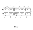
- the optical transponder 10 includes the device 11 , the client-side 12 , and the line-side 13 .
- the device 11 may include any of, but not limited to, a circuit pack, line module, blade, printed circuit board, integrated circuit, and the like.
- the device 11 is a physical housing for the optics and electronics associated with the transponder 10 or a circuit in which the optics and electronics are formed therein.
- the transponder 10 provides a bi-directional interface between the client-side 12 and the line-side 13 .
- the client-side 12 includes a client-side optical transmitter (TX) 702 and a client-side optical receiver (RX) 704 .
- the line-side 13 includes a line-side optical transmitter (TX) 706 and a line-side optical receiver (RX) 708 .
- the TX 702 and the RX 704 are communicatively coupled to a client-side device as described herein. Collectively, the TX 702 and the RX 704 form a transceiver (TR) that provides bi-directional optical communication with the client-side device.
- the TR may include discrete or integrated components. Further, the TR may include a pluggable device such as a daughterboard or the like.
- the RX 704 may include a wide-band optical receiver capable of receiving an optical signal at a plurality of different wavelengths such as 1250 nm to 1600 nm and to convert the received optical signal into a serial electrical signal.
- the TX 702 may include any type of optical transmitter including a short-reach, 1310 nm transmitter, a 1550 nm longer reach transmitter, a WDM transmitter, and the like.
- the TX 702 also includes a modulator to modulate a data signal onto a laser and optionally a wavelength locker to maintain a precise operating wavelength of the laser.
- the TX 706 and the RX 708 are communicatively coupled to a line-side device as described herein. Collectively, the TX 706 and the RX 708 form a transceiver (TR) that provides bi-directional optical communication with the line-side device.
- the line-side device may include some type of optical combiner/splitter that combines/splits a WDM signal from the TX 706 and the RX 708 with other WDM signals at other wavelengths in a WDM wavelength channel plan.
- the RX 708 may include a wide-band optical receiver capable of receiving an optical signal at a plurality of different wavelengths such as 1250 nm to 1600 nm and to convert the received optical signal into a serial electrical signal.
- the RX 708 may include a quadrature modulation receiver (or multiple receivers for polarization multiplexed systems) that utilizes DPSK, DQPSK, etc.
- the TX 706 may include a WDM transmitter capable of transmitting a WDM wavelength based on an associated WDM wavelength channel plan (or tuning to a plurality of wavelengths within the channel plan).
- the TX 706 may include an NRZ or RZ OOK transmitter.
- the TX 706 may include a quadrature modulation transmitter (or multiple transmitters for polarization multiplexed systems) that utilizes DPSK, DQPSK, etc.
- the optical transponder 10 further includes electrical circuitry forming SERDES 712 , 714 , 716 , 718 and framer/FEC/Clock and Data Recovery (CDR) 720 , 722 .
- These various electrical circuits are configured to prepare a data signal for remodulation, process overhead data, provide protocol encapsulation and framing, process forward error correction, provide 2R/3R functionality, and the like.
- the SERDES 712 , 714 , 716 , 718 are parallel-to-serial conversion circuits. Specifically, for high-speed systems (10 Gb/s, 40 Gb/s, 100 Gb/s, etc.) it is difficult to electrically process a data signal serially.
- the SERDES 712 , 714 , 716 , 718 convert a serial signal into a parallel signal for electrical processing.
- the framer/FEC/Clock and Data Recovery (CDR) 720 , 722 may be configured to perform various electrical functions on the parallel signal including framing with OTN, SONET/SDH, etc., processing of overhead data such as in an OTN or SONET/SDH frame, encoding of the parallel signal for quadrature modulation, processing of forward error correction, and the like.
- the RX 704 is configured to receive a signal from the client-side 12 , convert the signal from optical to electrical, and provide the electrical signal to the SERDES 716 .
- the SERDES 716 converts the electrical signal into a plurality of lower speed signals and provides these lower speed signals to the framer/FEC/Clock and Data Recovery 722 for processing. Once processed, the framer/FEC/Clock and Data Recovery 722 provides the processed lower speed signals to the SERDES 718 which converts the lower speed signals into one or more higher speed signals for the TX 706 to modulate an optical signal for transmission to the line-side 13 .
- the RX 708 provides similar functions from the line-side 13 to the client-side 12 .
- an example transponder 10 is illustrated connected to a client-side device 802 .
- the client-side device 802 may include an Ethernet, SDH/SONET, OTN, ATM, IP, Fibre Channel, etc. network element.
- the client-side device 802 may include a transmitter 804 transmitting a client-side signal to the transponder 10 at any wavelength between 1250 to 1600 nm and a receiver 806 receiving the client-side signal from the transponder 10 at a short reach 1310 nm wavelength.
- the client-side signal may be any type of high-rate signal such as a 10 Gb/s, 40 Gb/s, 100 Gb/s, etc. signal.
- the transponder 10 utilizes SONET, but those of ordinary skill in the art will recognize the transponder 10 may also use SDH, OTN, or the like.
- the client-side transmitter 804 connects to a short-reach receiver 810 on the transponder 10 that is configured to provide optical-to-electrical conversion of the client-side signal and provide the converted signal to a SERDES 812 that converts the signal to a plurality of lower speed signals for processing by the CDR 814 .
- the CDR 814 is configured to provide 3R transponder functionality as described herein including overhead processing.
- a SERDES 816 serializes the signal and provides the signal to an external optical modulator 818 .
- the external optical modulator 818 receives a laser signal from a laser 820 and modulates the laser signal with the signal from the SERDES 816 .
- the laser 820 provides a constant laser output at a particular WDM wavelength (e.g., 15XX.XX, 1 of N channels).
- the laser 820 is configured to tune over a band of WDM wavelengths.
- the transponder 10 includes a wavelength control device 822 that monitors and corrects changes in the WDM wavelength of the laser 820 .
- the wavelength control device 822 is generally referred to as a wavelength locker.
- the external optical modulator 818 may provide any type of modulation on the laser signal including, but not limited to, NRZ-OOK, RZ-OOK, RZ-DPSK, RZ-DQPSK, Polarization multiplexing, and the like.
- the client-side receiver 806 connects to a short-reach transmitter 830 (e.g., a laser diode (LD)) on the transponder 10 that is configured to provide a line-side signal to the client-side device 802 .
- the transmitter 830 receives the line-side signal from a SERDES 832 that converts the line-side signal from a plurality of lower speed signals.
- the SERDES 832 receives the plurality of lower speed signals from a CDR 834 which processing the lower speed signals such as providing 3R transponder functionality as described herein including overhead processing.
- the CDR 834 may provide B1/J0 byte monitoring in SONET overhead through a monitor circuit 835 (that may also be part of the CDR 834 ).
- the CDR 834 receives the lower speed signals from a SERDES 836 which provides the lower speed signals from the line-side signal received from a receiver 838 .
- the transponder 10 may include a processor 850 which is communicatively coupled to the various components, electronics, and optics in the transponder 10 .
- the processor 850 may include hardware, software, and/or firmware for operating the transponder 10 and monitoring and reporting events, statistics, and other data associated with the transponder to an external management device, module, etc.
- the transponder 10 may be physically realized in a device 860 .
- the device 860 may be a line module with a circuit board including one or more transponders 10 .
- the device 860 may be an integrated circuit with one or more transponders 10 .
- a transponder 10 is illustrated supporting RZ-DQPSK for high-speed applications.
- the high-speed applications may include 100 Gb/s Infiniband and/or Ethernet as described in parent application Ser. No. 12/166,537, “High-Speed Optical Transceiver for Infiniband and Ethernet).
- the transponder 10 of FIG. 9 includes three sections, a client interface 902 , a DQPSK demodulator 904 , and a DQPSK modulator 906 .
- the client interface 902 includes optics and electronics to interface to the client-side 12 .
- the client interface 902 may include one or more transceivers (TR) 910 that provide one or more clients signals.
- TR transceivers
- the transceivers 910 may be serial or parallel.
- the transceivers 910 may include a plurality of pluggable modules (e.g., XFPs), 12 ⁇ DDR (Double Data Rate) interfaces, and the like.
- the transceivers 910 provide an electrical signal to a switch/OTU/FEC circuit 912 that is generally configured to provide SERDES functionality, possibly payload mapping such as into Generic Framing Protocol (GFP), mapping into an OTN frame, forward error correcting, and the like.
- GFP Generic Framing Protocol
- the switch/OTU/FEC circuit 912 may interface with the DQPSK demodulator 904 and the DQPSK modulator 906 via SERDES Framer Interface Level 5 (SFI-5) interfaces 914 .
- SFI-5 SERDES Framer Interface Level 5
- SFI-5 is described in “Serdes Framer Interface Level 5 (SFI-5): Implementation Agreement for 40 Gb/s Interface for Physical Layer Devices” dated Jan. 29, 2002 from the Optical Internetworking Forum, the contents of which are incorporated by reference herein.
- the DQPSK demodulator 904 receives a line-side signal from the line-side 13 and demodulates the line-side signal for the client interface 902 .
- the DQPSK demodulator 904 includes an optical splitter 920 that is configured to receive the line-side signal and split it to two separate balanced receivers 922 , 924 .
- the balanced receiver 922 provides demodulation of an in-phase signal (I) and the balanced receiver 924 provides demodulation of a quadrature signal (Q).
- the balanced receivers 922 , 924 include a balanced detector and interferometer that connects to a bias and provides a copy of the input to provide differential detection with two photo-detectors and a summer.
- the balanced receivers 922 , 924 provide an electrical output to demultiplexers 926 , 928 that demultiplex the signal, provide clock and data recovery and provides a clock to a clock multiplier 930 (which is used in the DQPSK modulator 906 ).
- the demultiplexers 926 , 928 may connect to the client interface 902 via the SFI-5 interfaces 914 .
- the DQPSK modulator 906 is configured to provide the line-side signal from the client interface 902 .
- the DQPSK modulator 906 receives the client-side signal from the SFI-5 interfaces 914 which interface to multiplexers 940 , 942 (one for the I and the Q signal).
- the multiplexers 940 , 944 provide outputs to a DQPSK precoder 946 for multicarrier modulation (MCM) which precodes the Data (Dq and Di) for modulation.
- MCM multicarrier modulation
- the DQPSK modulator 906 includes a delay on the Dq line which connects to a phase modulator (PM) 950 .
- PM phase modulator
- the Di line connects to a Mach Zehnder modulator (MZM) 952 which connects to the PM 950 also through a delay.
- MZM Mach Zehnder modulator
- a laser 960 connects to the MZM 952 through an MZM pulse carver 962 .
- the clock multiplier 930 is provided to various components in the DQPSK modulator 906 .
- a transponder 10 is illustrated supporting polarization multiplexed DQPSK for high-speed applications. Similar to the transponder 10 of FIG. 9 , the transponder 10 of FIG. 10 includes a client interface 902 , a pol-mux DQPSK demodulator 1002 , and a pol-mux DQPSK modulator 1004 .
- the client interface 902 is substantially the same as described in FIG. 9 , but may include an SFI-5.1+ interface.
- the transponder 10 may be configured to support 112 Gb/s through a 28 Gb/s signal that utilizes DQPSK providing 56 Gb/s throughput and utilizing horizontal (H) and vertical (V) polarizations providing 112 Gb/s throughput.
- the transponder 10 may support 100 Gb/s client data through an OTN wrapper.
- the pol-mux DQPSK demodulator 1002 is similar to the DQPSK demodulator 904 but includes a polarization beam splitter (PBS) 1010 which splits the horizontal and vertical polarizations to separate demodulators 1012 , 1014 .
- PBS polarization beam splitter
- Each of the demodulators 1012 , 1014 includes similar components as the demodulator 904 , but performs demodulation for both I and Q signals for its respective polarization.
- Outputs of the demodulators 1012 , 1014 connect to demultiplexers 1016 , 1018 which provide a clock and electrical signal outputs (such as via the SFI-5.1+ interface) to the client interface 902 .
- the pol-mux DQPSK modulator 1004 receives the client-side signal from the client interface 902 such as via the SFI-5.1+ interface at multiplexers 1020 , 1022 .
- the multiplexers 1020 , 1022 format the I and Q data for modulation on each of the horizontal and vertical polarizations.
- the pol-mux DQPSK modulator 1004 includes two modulators 1024 , 1026 each modulating one of the horizontal and vertical polarizations.
- the modulator 1024 receives I and Q data from the multiplexer 1020 and the modulator 1026 receives I and Q data from the multiplexer 1022 .
- a tunable laser 1030 provides a laser signal to the modulators 1024 , 1026 through a PBS 1032 .
- the modulators 1024 , 1026 include phase modulators connected to the I and Q data and a delay. Outputs of the modulators 1024 , 1026 are combined via a PBS 1034 and then provided to an optical polarization
- an integrated circuit 1100 is illustrated depicting integration of some components of the transponder 10 .
- the integrated circuit 1100 may include a Complementary metal-oxide-semiconductor (CMOS) wafer.
- CMOS Complementary metal-oxide-semiconductor
- the integrated circuit 1100 may leverage existing CMOS fabrication plants, infrastructure, technology, etc.
- CMOS i.e., silicon
- CMOS provides various performance improvements in optical components as well as reducing cost, reducing footprint, etc.
- CMOS has ultra-high optical index contrast providing very low bending loss and compact devices
- CMOS has high performance actives and uses very low power for high optical and electrical confinement and small active device volumes, etc.
- CMOS provides a good solution for reducing packaging size and cost.
- CMOS may integrate optical modulation, drivers, receivers, radio frequency (RF) amps, digital circuitry for electrical signal processing, etc. with minimal electrical parasitics, loss, and power.
- CMOS in the same package may also integrate optical filters, arrayed waveguide gratings (AWGs), optical couplers, splitters, etc.
- CMOS may include optical or electrical switching components such as required in a ROADM.
- the CMOS wafer may include Germanium (Ge) spots, and the only thing external may be the laser.
- CMOS also has large available wafer real estate and near perfect yield. Further, silicon has ⁇ 2 ⁇ better ( ⁇ 149 W/m/K) thermal conductivity relative to InP (68)—easier component cooling.
- the exemplary integrated circuit 1100 includes both a modulator 1102 and a demodulator 1104 section on the same CMOS wafer.
- the modulator 1102 includes a QAM Mach-Zehnder modulator (MZM) 1110 in the wafer connected to an RF driver 1112 that receives a data input (Din) for modulating the MZM 1110 and a bias control 1114 circuit for controlling the MZM 1110 .
- a laser 1120 is external to the circuit 1100 but can connect to the MZM 1110 .
- an output of the MZM 1110 is shown connecting to an external multiplexer 1122 , however the multiplexer 1122 may also be realized in the integrated circuit 1100 .
- the demodulator 1104 receives a line-side signal from a demultiplexer 1124 into a 90-Degree Optical Hybrid mixer 1130 in the circuit 1100 .
- a Ge PIN 1132 detects the outputs of the 90-Degree Optical Hybrid mixer 1130 and the output is amplified by a transimpedance amplifier (TIA) 1134 .
- TIA transimpedance amplifier
- a Signal Processor+ CDR 1136 receives the output of the TIA 1134 and may provide electrical signal processing such as dispersion equalization, polarization mode dispersion compensation, and mitigation of other non-linear effects.
- the output signal may be provides to an OTN/FEC circuit 1140 that is illustrated outside of the circuit 1100 but may also be integrated within the circuit 1100 .
Abstract
Description
| TABLE 1 | |||
| Channel Number | Wavelength (nm) | ||
| 1 | 1557.36 | ||
| 2 | 1556.56 | ||
| 3 | 1555.75 | ||
| 4 | 1554.94 | ||
| 5 | 1554.13 | ||
| 6 | 1553.33 | ||
| 7 | 1552.52 | ||
| 8 | 1551.72 | ||
| 9 | 1550.92 | ||
| 10 | 1550.12 | ||
| 11 | 1549.32 | ||
| 12 | 1548.51 | ||
| 13 | 1547.72 | ||
| 14 | 1546.92 | ||
| 15 | 1546.12 | ||
| 16 | 1545.32 | ||
| TABLE 2 | ||
| Frequency | ||
| Ch. | (GHz) | Wavelength (nm) |
| 1 | 190,100 | 1577.03 |
| 2 | 190,200 | 1576.20 |
| 3 | 190,300 | 1575.37 |
| 4 | 190,400 | 1574.54 |
| 5 | 190,500 | 1573.71 |
| 6 | 190,600 | 1572.89 |
| 7 | 190,700 | 1572.06 |
| 8 | 190,800 | 1571.24 |
| 9 | 190,900 | 1570.42 |
| 10 | 191,000 | 1569.59 |
| 11 | 191,100 | 1568.77 |
| 12 | 191,200 | 1567.95 |
| 13 | 191,300 | 1567.13 |
| 14 | 191,400 | 1566.31 |
| 15 | 191,500 | 1565.50 |
| 16 | 191,600 | 1564.68 |
| 17 | 191,700 | 1563.86 |
| 18 | 191,800 | 1563.05 |
| 19 | 191,900 | 1562.23 |
| 20 | 192,000 | 1561.42 |
| 21 | 192,100 | 1560.61 |
| 22 | 192,200 | 1559.79 |
| 23 | 192,300 | 1558.98 |
| 24 | 192,400 | 1558.17 |
| 25 | 192,500 | 1557.36 |
| 26 | 192,600 | 1556.55 |
| 27 | 192,700 | 1555.75 |
| 28 | 192,800 | 1554.94 |
| 29 | 192,900 | 1554.13 |
| 30 | 193,000 | 1553.33 |
| 31 | 193,100 | 1552.52 |
| 32 | 193,200 | 1551.72 |
| 33 | 193,300 | 1550.92 |
| 34 | 193,400 | 1550.12 |
| 35 | 193,500 | 1549.32 |
| 36 | 193,600 | 1548.51 |
| 37 | 193,700 | 1547.72 |
| 38 | 193,800 | 1546.92 |
| 39 | 193,900 | 1546.12 |
| 40 | 194,000 | 1545.32 |
| 41 | 194,100 | 1544.53 |
| 42 | 194,200 | 1543.73 |
| 43 | 194,300 | 1542.94 |
| 44 | 194,400 | 1542.14 |
| 45 | 194,500 | 1541.35 |
| 46 | 194,600 | 1540.56 |
| 47 | 194,700 | 1539.77 |
| 48 | 194,800 | 1538.98 |
| 49 | 194,900 | 1538.19 |
| 50 | 195,000 | 1537.40 |
| 51 | 195,100 | 1536.61 |
| 52 | 195,200 | 1535.82 |
| 53 | 195,300 | 1535.04 |
| 54 | 195,400 | 1534.25 |
| 55 | 195,500 | 1533.47 |
| 56 | 195,600 | 1532.68 |
| 57 | 195,700 | 1531.90 |
| 58 | 195,800 | 1531.12 |
| 59 | 195,900 | 1530.33 |
| 60 | 196,000 | 1529.55 |
| 61 | 196,100 | 1528.77 |
| 62 | 196,200 | 1527.99 |
| 63 | 196,300 | 1527.22 |
| 64 | 196,400 | 1526.44 |
| 65 | 196,500 | 1525.66 |
| 66 | 196,600 | 1524.89 |
| 67 | 196,700 | 1524.11 |
| 68 | 196,800 | 1523.34 |
| 69 | 196,900 | 1522.56 |
| 70 | 197,000 | 1521.79 |
| 71 | 197,100 | 1521.02 |
| 72 | 197,200 | 1520.25 |
| 73 | 197,300 | 1519.48 |
Claims (17)
Priority Applications (4)
| Application Number | Priority Date | Filing Date | Title |
|---|---|---|---|
| US12/889,158 US9191117B2 (en) | 1995-05-11 | 2010-09-23 | High-speed optical transponder systems |
| US13/711,155 US9124383B1 (en) | 2010-09-23 | 2012-12-11 | High capacity fiber-optic integrated transmission and switching systems |
| US14/840,387 US9866929B2 (en) | 2010-09-23 | 2015-08-31 | High capacity fiber-optic integrated transmission systems |
| US15/833,108 US10194221B2 (en) | 2010-09-23 | 2017-12-06 | High capacity fiber-optic integrated transmission and switching systems |
Applications Claiming Priority (12)
| Application Number | Priority Date | Filing Date | Title |
|---|---|---|---|
| US08/438,844 US5504609A (en) | 1995-05-11 | 1995-05-11 | WDM optical communication system with remodulators |
| US08/624,269 US5726784A (en) | 1995-05-11 | 1996-03-29 | WDM optical communication system with remodulators and diverse optical transmitters |
| US08/669,049 US5715076A (en) | 1995-05-11 | 1996-06-24 | Remodulating channel selectors for WDM optical communication systems |
| US95505897A | 1997-10-21 | 1997-10-21 | |
| US09/428,420 US6233077B1 (en) | 1995-05-11 | 1999-10-28 | Remodulating channel selectors for WDM optical communication systems |
| US09/793,645 US6618176B2 (en) | 1995-05-11 | 2001-02-26 | Remodulating channel selectors for WDM optical communication systems |
| US10/618,684 US7369780B2 (en) | 1995-05-11 | 2003-07-15 | Remodulating channel selectors for WDM optical communication systems |
| US95003207P | 2007-07-16 | 2007-07-16 | |
| US12/099,479 US7809270B2 (en) | 1995-05-11 | 2008-04-08 | Remodulating channel selectors for WDM optical communication systems |
| US12/166,537 US8805195B2 (en) | 2007-07-16 | 2008-07-02 | High-speed optical transceiver for InfiniBand and Ethernet |
| US12/862,419 US8306424B2 (en) | 1995-05-11 | 2010-08-24 | Remodulating channel selectors for WDM optical communication systems |
| US12/889,158 US9191117B2 (en) | 1995-05-11 | 2010-09-23 | High-speed optical transponder systems |
Related Parent Applications (3)
| Application Number | Title | Priority Date | Filing Date |
|---|---|---|---|
| US12/099,479 Continuation-In-Part US7809270B2 (en) | 1995-05-11 | 2008-04-08 | Remodulating channel selectors for WDM optical communication systems |
| US12/166,537 Continuation-In-Part US8805195B2 (en) | 1995-05-11 | 2008-07-02 | High-speed optical transceiver for InfiniBand and Ethernet |
| US12/862,419 Continuation-In-Part US8306424B2 (en) | 1995-05-11 | 2010-08-24 | Remodulating channel selectors for WDM optical communication systems |
Related Child Applications (2)
| Application Number | Title | Priority Date | Filing Date |
|---|---|---|---|
| US08/624,269 Continuation-In-Part US5726784A (en) | 1995-05-11 | 1996-03-29 | WDM optical communication system with remodulators and diverse optical transmitters |
| US13/711,155 Continuation-In-Part US9124383B1 (en) | 2010-09-23 | 2012-12-11 | High capacity fiber-optic integrated transmission and switching systems |
Publications (2)
| Publication Number | Publication Date |
|---|---|
| US20110013911A1 US20110013911A1 (en) | 2011-01-20 |
| US9191117B2 true US9191117B2 (en) | 2015-11-17 |
Family
ID=43465386
Family Applications (1)
| Application Number | Title | Priority Date | Filing Date |
|---|---|---|---|
| US12/889,158 Expired - Fee Related US9191117B2 (en) | 1995-05-11 | 2010-09-23 | High-speed optical transponder systems |
Country Status (1)
| Country | Link |
|---|---|
| US (1) | US9191117B2 (en) |
Cited By (11)
| Publication number | Priority date | Publication date | Assignee | Title |
|---|---|---|---|---|
| US20160103286A1 (en) * | 2014-10-10 | 2016-04-14 | Sumitomo Electric Industries, Ltd. | Optical transceiver implementing erbium doped fiber amplifier |
| US11184234B2 (en) | 2019-04-16 | 2021-11-23 | Ciena Corporation | Self-optimizing fabric architecture and self-assembling network |
| US11196504B1 (en) | 2020-10-28 | 2021-12-07 | Ciena Corporation | Extending the optical spectrum of an optical network |
| US11211707B1 (en) | 2020-11-13 | 2021-12-28 | Lyteloop Technologies, Llc | Apparatus for broadband wavelength conversion of dual-polarization phase-encoded signal |
| US11346923B1 (en) | 2020-11-13 | 2022-05-31 | Lyteloop Technologies, Llc | LiDAR system implementing wavelength conversion |
| US11488646B2 (en) | 2019-11-13 | 2022-11-01 | Samsung Electronics Co., Ltd. | Encoders, decoders, and semiconductor memory devices including the same |
| US11553259B2 (en) | 2020-10-28 | 2023-01-10 | Ciena Corporation | Extending the optical spectrum of an optical network |
| US11641247B2 (en) | 2003-06-10 | 2023-05-02 | Alexander Soto | System and method for performing high-speed communications over fiber optical networks |
| US11646811B2 (en) | 2021-10-08 | 2023-05-09 | Zayo Group, LCC | Alien wavelength management |
| US11711270B1 (en) | 2022-04-19 | 2023-07-25 | Ciena Corporation | Creating an optimal node interconnect topology given certain constraints |
| US11799549B2 (en) | 2021-08-13 | 2023-10-24 | Ciena Corporation | Express mesh intersatellite optical coherent networking |
Families Citing this family (68)
| Publication number | Priority date | Publication date | Assignee | Title |
|---|---|---|---|---|
| US6721508B1 (en) * | 1998-12-14 | 2004-04-13 | Tellabs Operations Inc. | Optical line terminal arrangement, apparatus and methods |
| US7620327B2 (en) * | 2001-07-09 | 2009-11-17 | Oyster Optics, Inc. | Fiber optic telecommunications card with energy level monitoring |
| US6937666B2 (en) * | 2002-12-20 | 2005-08-30 | Bridgewave Communications, Inc. | Wideband digital radio with transmit modulation cancellation |
| US8731007B2 (en) * | 2005-12-30 | 2014-05-20 | Remec Broadband Wireless, Llc | Digital microwave radio link with a variety of ports |
| US8711888B2 (en) * | 2005-12-30 | 2014-04-29 | Remec Broadband Wireless Llc | Digital microwave radio link with adaptive data rate |
| US10128953B2 (en) | 2006-10-13 | 2018-11-13 | Menara Networks, Inc. | High-speed pluggable optical transceivers with advanced functionality |
| US8929744B2 (en) * | 2006-10-13 | 2015-01-06 | Menara Networks, Inc. | 40G/100G MSA-compliant optical transceivers with advanced functionality |
| US9319143B2 (en) | 2006-10-13 | 2016-04-19 | Menara Networks, Inc. | 40G/100G/200G/400G pluggable optical transceivers with advanced functionality |
| WO2009105281A2 (en) * | 2008-02-22 | 2009-08-27 | Opvista Incorporated | Spectrally efficient parallel optical wdm channels for long-haul man and wan optical networks |
| US20090290877A1 (en) * | 2008-05-21 | 2009-11-26 | Nec Laboratories America, Inc. | Monitoring for High Speed OFDM Signal Transmission |
| US20090290878A1 (en) * | 2008-05-22 | 2009-11-26 | Nec Laboratories America, Inc. | Generating an Optical OFDM Signal with Reduced OSNR Requirement |
| TWI382684B (en) * | 2008-11-07 | 2013-01-11 | Univ Nat Chiao Tung | Dual Service Fiber Capture System |
| US8831437B2 (en) * | 2009-09-04 | 2014-09-09 | Luxtera, Inc. | Method and system for a photonic interposer |
| CN101814953B (en) * | 2010-03-01 | 2014-03-19 | 中兴通讯股份有限公司 | Method and system for realizing automatic protection switching of transmission equipment |
| US20110299858A1 (en) * | 2010-06-08 | 2011-12-08 | Cisco Technology, Inc. | Host device with multipurpose optics drive capabilities |
| CN103039022B (en) * | 2010-07-01 | 2016-04-27 | 北阳电机株式会社 | Light data transmission set, optical communication equipment and automatic transportation equipment |
| US9124383B1 (en) | 2010-09-23 | 2015-09-01 | Ciena Corporation | High capacity fiber-optic integrated transmission and switching systems |
| US9054808B2 (en) * | 2010-10-08 | 2015-06-09 | Infinera Corporation | Controlled depolarization using chirp for mitigation of nonlinear polarization scattering |
| US8687971B2 (en) * | 2011-01-31 | 2014-04-01 | Telefonaktiebolaget Lm Ericsson (Publ) | System, laser-on-CMOS chip, and method for setting a wavelength to be used by the laser-on-CMOS chip |
| US10009108B2 (en) | 2011-02-11 | 2018-06-26 | Menara Networks, Inc. | Coherent and pulse amplitude modulation in a pluggable optical transceiver |
| US20120251111A1 (en) * | 2011-03-31 | 2012-10-04 | Nec Laboratories America, Inc. | Optoelectronic wavelength converter for polarization multiplexed optical signals |
| US8768167B2 (en) | 2011-04-29 | 2014-07-01 | Telcordia Technologies, Inc. | System and method for automated provisioning of services using single step routing and wavelength assignment algorithm in DWDM networks |
| US8886055B1 (en) * | 2011-05-24 | 2014-11-11 | Clariphy Communications, Inc. | Reduced data rate operation mode for high speed optical communication device |
| US9143227B2 (en) | 2011-11-07 | 2015-09-22 | Ciena Corporation | Optical transport network port protection systems and methods using flexible switch criteria |
| US9054796B2 (en) * | 2011-11-17 | 2015-06-09 | Finisar Corporation | Dual optical electrical conversion module |
| US9490931B2 (en) * | 2011-12-22 | 2016-11-08 | Telefonaktiebolaget Lm Ericsson (Publ) | Muxponder and method of converting a plurality of tributary optical communications signals having a first bit rate into an optical line signal having a second, higher bit rate |
| US9374166B2 (en) * | 2012-02-13 | 2016-06-21 | Ciena Corporation | High speed optical communication systems and methods with flexible bandwidth adaptation |
| US9455788B2 (en) | 2014-02-10 | 2016-09-27 | Ciena Corporation | Hitless modulation scheme change systems and methods in optical networks |
| US9258190B2 (en) | 2014-02-10 | 2016-02-09 | Ciena Corporation | Systems and methods for managing excess optical capacity and margin in optical networks |
| US10257596B2 (en) | 2012-02-13 | 2019-04-09 | Ciena Corporation | Systems and methods for managing excess optical capacity and margin in optical networks |
| CN103312414B (en) * | 2012-03-16 | 2016-03-30 | 富士通株式会社 | A kind of inverse channel device and comprise the transmitter of this device, receiver and system |
| JP5799872B2 (en) * | 2012-03-28 | 2015-10-28 | 富士通株式会社 | Optical transmitter, optical receiver, and optical transmission method |
| US9130692B2 (en) * | 2012-04-23 | 2015-09-08 | Coriant Operations, Inc. | Reconfigurable optical add/drop multiplexer network element for C-band and L-band optical signals |
| US9882643B2 (en) | 2012-05-04 | 2018-01-30 | Deutsche Telekom Ag | Method and device for setting up and operating a modular, highly scalable, very simple, cost-efficient and enduring transparent optically routed network for network capacities of greater than 1 Petabit/s |
| EP2862304A4 (en) | 2012-05-16 | 2016-03-09 | Oe Solutions America Inc | Wavelength tunable array for data communications |
| US9088380B2 (en) | 2012-05-31 | 2015-07-21 | Ciena Corporation | Optical transport network generic non-client specific protection systems and methods |
| US9184846B2 (en) * | 2013-03-17 | 2015-11-10 | Finisar Corporation | Pluggable optical host and network I/O optoelectronic module |
| US9490899B1 (en) * | 2013-05-17 | 2016-11-08 | The United States Of America As Represented By The Administrator Of National Aeronautics And Space Administration | Optical tunable-based transmitter for multiple radio frequency bands |
| US9225422B1 (en) * | 2013-07-11 | 2015-12-29 | Inphi Corporation | Integrated control module for communication system on a chip for silicon photonics |
| US9166704B1 (en) * | 2013-07-17 | 2015-10-20 | Inphi Corporation | Integrated control for silicon photonics |
| US9413520B2 (en) | 2013-12-12 | 2016-08-09 | Ciena Corporation | Optical transceiver and method with channel binding, clock forwarding, and integrate-and-dump receivers |
| US9414135B2 (en) * | 2013-12-24 | 2016-08-09 | Nec Corporation | Flexible-client, flexible-line interface transponder |
| WO2015124952A1 (en) | 2014-02-24 | 2015-08-27 | Rockley Photonics Limited | Detector remodulator and optoelectronic switch |
| US10928659B2 (en) | 2014-02-24 | 2021-02-23 | Rockley Photonics Limited | Optoelectronic device |
| US11133866B2 (en) | 2014-02-25 | 2021-09-28 | Pharmaseq, Inc. | All optical identification and sensor system with power on discovery |
| US9503443B2 (en) | 2014-09-15 | 2016-11-22 | Ciena Corporation | Secure access systems and methods to network elements operating in a network |
| US11150494B2 (en) | 2015-03-05 | 2021-10-19 | Rockley Photonics Limited | Waveguide modulator structures |
| US10921616B2 (en) | 2016-11-23 | 2021-02-16 | Rockley Photonics Limited | Optoelectronic device |
| FR3036562A1 (en) * | 2015-05-20 | 2016-11-25 | Orange | TRANSPONDER FOR A FIBER RADIO TRANSMISSION SYSTEM FOR DELIVERING THE ANTENNA MANAGEMENT INTERFACE |
| US10630053B2 (en) | 2015-07-30 | 2020-04-21 | Optipulse Inc. | High power laser grid structure |
| EP3329562B1 (en) | 2015-07-30 | 2024-03-13 | Optipulse Inc. | Rigid high power and high speed lasing grid structures |
| US10882258B1 (en) | 2016-01-22 | 2021-01-05 | Pharmaseq, Inc. | Microchip affixing probe and method of use |
| US9831947B2 (en) | 2016-04-20 | 2017-11-28 | Ciena Corporation | Margin determination systems and methods in optical networks |
| US10171171B2 (en) * | 2016-07-07 | 2019-01-01 | Luxtera, Inc. | Method and system for selectable parallel optical fiber and wavelength division multiplexed operation |
| US10419120B2 (en) * | 2016-07-22 | 2019-09-17 | Lockheed Martin Corporation | Phased-array coherent transceiver |
| US11101256B2 (en) | 2016-11-23 | 2021-08-24 | Rockley Photonics Limited | Optical modulators |
| US11036006B2 (en) | 2016-12-02 | 2021-06-15 | Rockley Photonics Limited | Waveguide device and method of doping a waveguide device |
| US11105975B2 (en) | 2016-12-02 | 2021-08-31 | Rockley Photonics Limited | Waveguide optoelectronic device |
| WO2019033111A1 (en) | 2017-08-11 | 2019-02-14 | Optipulse Inc. | Laser grid structures for wireless high speed data transfers |
| US10374705B2 (en) | 2017-09-06 | 2019-08-06 | Optipulse Inc. | Method and apparatus for alignment of a line-of-sight communications link |
| US10454587B2 (en) * | 2017-11-22 | 2019-10-22 | Google Llc | Parallel optical transponder enabled by optical comb sources |
| US10313021B1 (en) | 2018-01-10 | 2019-06-04 | Ciena Corporation | High-efficiency self-resetting integrating optical transceiver |
| US10587339B1 (en) | 2018-11-27 | 2020-03-10 | Ciena Corporation | Systems and methods for achieving best effort home route capacity on protection paths during optical restoration |
| US10659854B1 (en) * | 2019-04-01 | 2020-05-19 | Adva Optical Networking Se | Pluggable aggregation module for an optical network |
| US10985837B2 (en) | 2019-06-17 | 2021-04-20 | Ciena Corporation | Generic non-client specific protection via TCM status and enhanced OTN network propagation of client faults |
| CN110391847A (en) * | 2019-07-25 | 2019-10-29 | 长春理工大学 | High-speed high capacity wireless memory device |
| US11546129B2 (en) * | 2020-02-14 | 2023-01-03 | P-Chip Ip Holdings Inc. | Light-triggered transponder |
| US11309984B2 (en) | 2020-03-04 | 2022-04-19 | Ciena Corporation | TCM control for physical layer on OTU ports |
Citations (70)
| Publication number | Priority date | Publication date | Assignee | Title |
|---|---|---|---|---|
| US4641371A (en) | 1985-01-16 | 1987-02-03 | Westinghouse Electric Corp. | Multi-star fiber optic network |
| US4677618A (en) | 1985-04-04 | 1987-06-30 | International Business Machines Corporation | Method and apparatus for deskewing WDM data transmitted through a dispersive medium |
| US4736120A (en) | 1983-12-12 | 1988-04-05 | Stc Plc | Timing extraction circuit |
| US4807222A (en) * | 1986-08-25 | 1989-02-21 | American Telephone And Telegraph Company At&T Bell Laboratories | Cordless accessed high-speed high-capacity local area networks |
| US4807227A (en) | 1986-10-15 | 1989-02-21 | Nec Corporation | Optical wavelength-division switching system with coherent optical detection system |
| EP0310058A2 (en) | 1987-09-30 | 1989-04-05 | Nec Corporation | Time and wavelength division switching system |
| US4886334A (en) | 1987-09-01 | 1989-12-12 | Nec Corporation | Optical amplifying repeater |
| US4933929A (en) * | 1987-06-29 | 1990-06-12 | Nec Corporation | Wavelength multiplexed optical transmitter for generating constant-amplitude angle-modulated beams to eliminate phase noise in adjacent transmission channels |
| US4945531A (en) | 1986-04-17 | 1990-07-31 | Nec Corporation | Optical wavelength-division multiplex transmission system with an optical filter for spontaneous emission noise |
| US4955014A (en) * | 1986-10-31 | 1990-09-04 | Alcatel N.V. | Broadband optical communication system, particularly in the subscriber area |
| US4957339A (en) * | 1988-06-08 | 1990-09-18 | Alcatel N.V. | Optical communication system, particularly in the subscriber area |
| US4989199A (en) | 1988-10-31 | 1991-01-29 | At&T Bell Laboratories | Photonic switch architecture utilizing code and wavelength multiplexing |
| US5005936A (en) * | 1990-05-22 | 1991-04-09 | Hughes Aircraft Company | Long range bidirectional optical fiber communication link |
| EP0436292A2 (en) | 1990-01-02 | 1991-07-10 | AT&T Corp. | Programmable multiplexing techniques for mapping a capacity domain into a time domain within a frame |
| EP0438022A2 (en) | 1990-01-18 | 1991-07-24 | International Business Machines Corporation | Method for deskewing bits in a communication system using wavelength division multiplexing |
| US5050952A (en) | 1989-03-31 | 1991-09-24 | Alcatel N. V. | Optical communications system for diplex or duplex transmission |
| US5065396A (en) | 1990-01-02 | 1991-11-12 | At&T Bell Laboratories | Inverse multiplexer and demultiplexer techniques |
| EP0488241A2 (en) | 1990-11-30 | 1992-06-03 | Hitachi, Ltd. | Optical frequency division multiplexing network |
| US5140456A (en) | 1991-04-08 | 1992-08-18 | General Instrument Corporation | Low noise high power optical fiber amplifier |
| WO1992018890A1 (en) | 1991-04-22 | 1992-10-29 | The Trustees Of Columbia University In The City Of New York | Optical communications system and method |
| US5166821A (en) | 1991-03-12 | 1992-11-24 | General Instrument Corporation | Reduction of non-linear effects in optical fiber communication systems and method of using same |
| US5185736A (en) | 1989-05-12 | 1993-02-09 | Alcatel Na Network Systems Corp. | Synchronous optical transmission system |
| US5200964A (en) | 1991-03-12 | 1993-04-06 | General Instrument Corporation | Broad linewidth lasers for optical fiber communication systems |
| US5218465A (en) * | 1991-09-03 | 1993-06-08 | Motorola, Inc. | Intelligent interconnects for broadband optical networking |
| US5257124A (en) | 1991-08-15 | 1993-10-26 | General Instrument Corporation | Low distortion laser system for AM fiber optic communication |
| US5267073A (en) | 1989-10-30 | 1993-11-30 | Pirelli Cavi S.P.A. | Amplifier adapter for optical lines |
| US5271024A (en) | 1992-07-27 | 1993-12-14 | General Instrument Corporation | Optical fiber amplifier and laser with flattened gain slope |
| US5282257A (en) * | 1990-12-28 | 1994-01-25 | Fuji Xerox Co., Ltd. | Star coupler and optical communication network |
| US5283686A (en) | 1992-07-27 | 1994-02-01 | General Instrument Corporation, Jerrold Communications | Optical systems with grating reflector |
| US5295209A (en) | 1991-03-12 | 1994-03-15 | General Instrument Corporation | Spontaneous emission source having high spectral density at a desired wavelength |
| US5321541A (en) * | 1991-12-12 | 1994-06-14 | At&T Bell Laboratories | Passive optical communication network with broadband upgrade |
| US5321543A (en) | 1992-10-20 | 1994-06-14 | General Instrument Corporation | Apparatus and method for linearizing an external optical modulator |
| US5339183A (en) | 1992-03-19 | 1994-08-16 | Fujitsu Limited | Optical signal transmission device |
| US5363229A (en) | 1990-11-26 | 1994-11-08 | Matsushita Electrical Industrial Co., Ltd. | Optical bus transmission system |
| US5387927A (en) * | 1993-09-17 | 1995-02-07 | Mpr Teltech Ltd. | Method and apparatus for broadband transmission from a central office to a number of subscribers |
| WO1995019689A1 (en) | 1994-01-18 | 1995-07-20 | British Telecommunications Public Limited Company | Interconnected passive optical networks |
| US5455699A (en) | 1993-12-21 | 1995-10-03 | At&T Corp. | Large capacity multi-access wavelength division multiplexing packet network |
| US5461622A (en) | 1994-06-14 | 1995-10-24 | Bell Communications Research, Inc. | Method and apparatus for using SONET overheat to align multiple inverse multiplexed data streams |
| US5465254A (en) * | 1985-04-24 | 1995-11-07 | Wilson; Philip D. | Ring-type communication network |
| US5465267A (en) | 1993-01-05 | 1995-11-07 | Nec Corporation | Error-correcting tandem encoding system |
| US5467212A (en) | 1993-06-04 | 1995-11-14 | Huber; David R. | Addressable grating modulation system for optical cable TV system |
| US5483372A (en) | 1994-11-29 | 1996-01-09 | International Business Machines Corporation | Single and multichannel transmission over long distances using repeated level-crossing remodulation |
| US5487120A (en) | 1994-02-09 | 1996-01-23 | International Business Machines Corporation | Optical wavelength division multiplexer for high speed, protocol-independent serial data sources |
| US5493625A (en) | 1993-11-16 | 1996-02-20 | At&T Corp. | Fast tunable channel dropping filter |
| US5504609A (en) | 1995-05-11 | 1996-04-02 | Ciena Corporation | WDM optical communication system with remodulators |
| US5510917A (en) * | 1990-12-18 | 1996-04-23 | Aster Products | Optical communication monitoring and control |
| US5532864A (en) | 1995-06-01 | 1996-07-02 | Ciena Corporation | Optical monitoring channel for wavelength division multiplexed optical communication system |
| US5557439A (en) | 1995-07-25 | 1996-09-17 | Ciena Corporation | Expandable wavelength division multiplexed optical communications systems |
| US5559910A (en) | 1994-06-06 | 1996-09-24 | Kokusai Denshin Denwa Kabushiki Kaisha | Wavelength division multiplexed optical fiber transmission equiptment |
| US5561682A (en) | 1994-02-14 | 1996-10-01 | Hitachi, Ltd. | Semiconductor optical device and method for fabricating the same |
| US5576875A (en) * | 1994-04-13 | 1996-11-19 | France Telecom | Telecommunications network organized in reconfigurable wavelength-division-multiplexed optical loops |
| US5600466A (en) * | 1994-01-26 | 1997-02-04 | British Telecommunications Public Limited Company | Wavelength division optical signalling network apparatus and method |
| US5608571A (en) | 1994-10-04 | 1997-03-04 | Northern Telecom Limited | Optical amplifiers |
| US5617236A (en) * | 1994-08-15 | 1997-04-01 | Actisys Corporation | Infrared communication device for multistandard operations |
| US5710650A (en) | 1996-03-14 | 1998-01-20 | Alcatel Network Systems, Inc. | Dispersion-reducing multiple wavelength division multiplexing optical fiber transceiver and methods for using and assembling same |
| US5715076A (en) | 1995-05-11 | 1998-02-03 | Ciena Corporation | Remodulating channel selectors for WDM optical communication systems |
| US5774244A (en) | 1994-01-18 | 1998-06-30 | British Telecommunications Public Limited Company | Optical communications networks |
| US5784184A (en) | 1995-05-11 | 1998-07-21 | Ciena Corporation | WDM Optical communication systems with remodulators and remodulating channel selectors |
| US5887039A (en) | 1993-12-16 | 1999-03-23 | Nec Corporation | Data transmission system using specific pattern for synchronization |
| US5938309A (en) | 1997-03-18 | 1999-08-17 | Ciena Corporation | Bit-rate transparent WDM optical communication system with remodulators |
| US6031644A (en) | 1996-11-25 | 2000-02-29 | Fujitsu Limited | Method, device, and system for controlling wavelength of optical signal |
| US6233077B1 (en) | 1995-05-11 | 2001-05-15 | Ciena Corporation | Remodulating channel selectors for WDM optical communication systems |
| US20030016697A1 (en) | 2001-07-19 | 2003-01-23 | Jordan Reuven D. | Method and apparatus for converting data packets between a higher bandwidth network and a lower bandwidth network having multiple channels |
| US20030091267A1 (en) | 2001-02-28 | 2003-05-15 | Alvarez Mario F. | Node management architecture with customized line card handlers for a modular optical network, and methods and apparatus therefor |
| US20040252720A1 (en) | 2003-06-10 | 2004-12-16 | Cisco Technology, Inc. | Fibre channel frame-mode GFP with distributed delimiter |
| US20060002304A1 (en) | 2004-06-30 | 2006-01-05 | Nortel Networks Limited | Method and apparatus for implementing link-based source routing in generic framing protocol |
| US20060268943A1 (en) | 2005-05-16 | 2006-11-30 | International Business Machines Corporation | Methods, systems, and storage media for data encapsulation in networks |
| US20070014308A1 (en) | 2005-07-17 | 2007-01-18 | Gunthorpe Jason G | Method to extend the physical reach of an infiniband network |
| US20080019463A1 (en) | 2006-07-19 | 2008-01-24 | Fujitsu Limited | Control method and apparatus for receiving optical signal |
| US7583599B1 (en) | 2004-09-27 | 2009-09-01 | Intel Corporation | Transporting stream client signals via packet interface using GFP mapping |
Family Cites Families (1)
| Publication number | Priority date | Publication date | Assignee | Title |
|---|---|---|---|---|
| DE19647334B4 (en) * | 1996-11-15 | 2004-07-15 | Benteler Ag | Side impact beam for a passenger car |
-
2010
- 2010-09-23 US US12/889,158 patent/US9191117B2/en not_active Expired - Fee Related
Patent Citations (71)
| Publication number | Priority date | Publication date | Assignee | Title |
|---|---|---|---|---|
| US4736120A (en) | 1983-12-12 | 1988-04-05 | Stc Plc | Timing extraction circuit |
| US4641371A (en) | 1985-01-16 | 1987-02-03 | Westinghouse Electric Corp. | Multi-star fiber optic network |
| US4677618A (en) | 1985-04-04 | 1987-06-30 | International Business Machines Corporation | Method and apparatus for deskewing WDM data transmitted through a dispersive medium |
| US5465254A (en) * | 1985-04-24 | 1995-11-07 | Wilson; Philip D. | Ring-type communication network |
| US4945531A (en) | 1986-04-17 | 1990-07-31 | Nec Corporation | Optical wavelength-division multiplex transmission system with an optical filter for spontaneous emission noise |
| US4807222A (en) * | 1986-08-25 | 1989-02-21 | American Telephone And Telegraph Company At&T Bell Laboratories | Cordless accessed high-speed high-capacity local area networks |
| US4807227A (en) | 1986-10-15 | 1989-02-21 | Nec Corporation | Optical wavelength-division switching system with coherent optical detection system |
| US4955014A (en) * | 1986-10-31 | 1990-09-04 | Alcatel N.V. | Broadband optical communication system, particularly in the subscriber area |
| US4933929A (en) * | 1987-06-29 | 1990-06-12 | Nec Corporation | Wavelength multiplexed optical transmitter for generating constant-amplitude angle-modulated beams to eliminate phase noise in adjacent transmission channels |
| US4886334A (en) | 1987-09-01 | 1989-12-12 | Nec Corporation | Optical amplifying repeater |
| EP0310058A2 (en) | 1987-09-30 | 1989-04-05 | Nec Corporation | Time and wavelength division switching system |
| US4957339A (en) * | 1988-06-08 | 1990-09-18 | Alcatel N.V. | Optical communication system, particularly in the subscriber area |
| US4989199A (en) | 1988-10-31 | 1991-01-29 | At&T Bell Laboratories | Photonic switch architecture utilizing code and wavelength multiplexing |
| US5050952A (en) | 1989-03-31 | 1991-09-24 | Alcatel N. V. | Optical communications system for diplex or duplex transmission |
| US5185736A (en) | 1989-05-12 | 1993-02-09 | Alcatel Na Network Systems Corp. | Synchronous optical transmission system |
| US5267073A (en) | 1989-10-30 | 1993-11-30 | Pirelli Cavi S.P.A. | Amplifier adapter for optical lines |
| US5065396A (en) | 1990-01-02 | 1991-11-12 | At&T Bell Laboratories | Inverse multiplexer and demultiplexer techniques |
| EP0436292A2 (en) | 1990-01-02 | 1991-07-10 | AT&T Corp. | Programmable multiplexing techniques for mapping a capacity domain into a time domain within a frame |
| US5157530A (en) | 1990-01-18 | 1992-10-20 | International Business Machines Corporation | Optical fiber system |
| EP0438022A2 (en) | 1990-01-18 | 1991-07-24 | International Business Machines Corporation | Method for deskewing bits in a communication system using wavelength division multiplexing |
| US5005936A (en) * | 1990-05-22 | 1991-04-09 | Hughes Aircraft Company | Long range bidirectional optical fiber communication link |
| US5363229A (en) | 1990-11-26 | 1994-11-08 | Matsushita Electrical Industrial Co., Ltd. | Optical bus transmission system |
| EP0488241A2 (en) | 1990-11-30 | 1992-06-03 | Hitachi, Ltd. | Optical frequency division multiplexing network |
| US5510917A (en) * | 1990-12-18 | 1996-04-23 | Aster Products | Optical communication monitoring and control |
| US5282257A (en) * | 1990-12-28 | 1994-01-25 | Fuji Xerox Co., Ltd. | Star coupler and optical communication network |
| US5166821A (en) | 1991-03-12 | 1992-11-24 | General Instrument Corporation | Reduction of non-linear effects in optical fiber communication systems and method of using same |
| US5200964A (en) | 1991-03-12 | 1993-04-06 | General Instrument Corporation | Broad linewidth lasers for optical fiber communication systems |
| US5295209A (en) | 1991-03-12 | 1994-03-15 | General Instrument Corporation | Spontaneous emission source having high spectral density at a desired wavelength |
| US5140456A (en) | 1991-04-08 | 1992-08-18 | General Instrument Corporation | Low noise high power optical fiber amplifier |
| WO1992018890A1 (en) | 1991-04-22 | 1992-10-29 | The Trustees Of Columbia University In The City Of New York | Optical communications system and method |
| US5257124A (en) | 1991-08-15 | 1993-10-26 | General Instrument Corporation | Low distortion laser system for AM fiber optic communication |
| US5218465A (en) * | 1991-09-03 | 1993-06-08 | Motorola, Inc. | Intelligent interconnects for broadband optical networking |
| US5321541A (en) * | 1991-12-12 | 1994-06-14 | At&T Bell Laboratories | Passive optical communication network with broadband upgrade |
| US5339183A (en) | 1992-03-19 | 1994-08-16 | Fujitsu Limited | Optical signal transmission device |
| US5271024A (en) | 1992-07-27 | 1993-12-14 | General Instrument Corporation | Optical fiber amplifier and laser with flattened gain slope |
| US5283686A (en) | 1992-07-27 | 1994-02-01 | General Instrument Corporation, Jerrold Communications | Optical systems with grating reflector |
| US5321543A (en) | 1992-10-20 | 1994-06-14 | General Instrument Corporation | Apparatus and method for linearizing an external optical modulator |
| US5465267A (en) | 1993-01-05 | 1995-11-07 | Nec Corporation | Error-correcting tandem encoding system |
| US5467212A (en) | 1993-06-04 | 1995-11-14 | Huber; David R. | Addressable grating modulation system for optical cable TV system |
| US5387927A (en) * | 1993-09-17 | 1995-02-07 | Mpr Teltech Ltd. | Method and apparatus for broadband transmission from a central office to a number of subscribers |
| US5493625A (en) | 1993-11-16 | 1996-02-20 | At&T Corp. | Fast tunable channel dropping filter |
| US5887039A (en) | 1993-12-16 | 1999-03-23 | Nec Corporation | Data transmission system using specific pattern for synchronization |
| US5455699A (en) | 1993-12-21 | 1995-10-03 | At&T Corp. | Large capacity multi-access wavelength division multiplexing packet network |
| WO1995019689A1 (en) | 1994-01-18 | 1995-07-20 | British Telecommunications Public Limited Company | Interconnected passive optical networks |
| US5774244A (en) | 1994-01-18 | 1998-06-30 | British Telecommunications Public Limited Company | Optical communications networks |
| US5600466A (en) * | 1994-01-26 | 1997-02-04 | British Telecommunications Public Limited Company | Wavelength division optical signalling network apparatus and method |
| US5487120A (en) | 1994-02-09 | 1996-01-23 | International Business Machines Corporation | Optical wavelength division multiplexer for high speed, protocol-independent serial data sources |
| US5561682A (en) | 1994-02-14 | 1996-10-01 | Hitachi, Ltd. | Semiconductor optical device and method for fabricating the same |
| US5576875A (en) * | 1994-04-13 | 1996-11-19 | France Telecom | Telecommunications network organized in reconfigurable wavelength-division-multiplexed optical loops |
| US5559910A (en) | 1994-06-06 | 1996-09-24 | Kokusai Denshin Denwa Kabushiki Kaisha | Wavelength division multiplexed optical fiber transmission equiptment |
| US5461622A (en) | 1994-06-14 | 1995-10-24 | Bell Communications Research, Inc. | Method and apparatus for using SONET overheat to align multiple inverse multiplexed data streams |
| US5617236A (en) * | 1994-08-15 | 1997-04-01 | Actisys Corporation | Infrared communication device for multistandard operations |
| US5608571A (en) | 1994-10-04 | 1997-03-04 | Northern Telecom Limited | Optical amplifiers |
| US5483372A (en) | 1994-11-29 | 1996-01-09 | International Business Machines Corporation | Single and multichannel transmission over long distances using repeated level-crossing remodulation |
| US5504609A (en) | 1995-05-11 | 1996-04-02 | Ciena Corporation | WDM optical communication system with remodulators |
| US5715076A (en) | 1995-05-11 | 1998-02-03 | Ciena Corporation | Remodulating channel selectors for WDM optical communication systems |
| US5784184A (en) | 1995-05-11 | 1998-07-21 | Ciena Corporation | WDM Optical communication systems with remodulators and remodulating channel selectors |
| US6233077B1 (en) | 1995-05-11 | 2001-05-15 | Ciena Corporation | Remodulating channel selectors for WDM optical communication systems |
| US5532864A (en) | 1995-06-01 | 1996-07-02 | Ciena Corporation | Optical monitoring channel for wavelength division multiplexed optical communication system |
| US5557439A (en) | 1995-07-25 | 1996-09-17 | Ciena Corporation | Expandable wavelength division multiplexed optical communications systems |
| US5710650A (en) | 1996-03-14 | 1998-01-20 | Alcatel Network Systems, Inc. | Dispersion-reducing multiple wavelength division multiplexing optical fiber transceiver and methods for using and assembling same |
| US6031644A (en) | 1996-11-25 | 2000-02-29 | Fujitsu Limited | Method, device, and system for controlling wavelength of optical signal |
| US5938309A (en) | 1997-03-18 | 1999-08-17 | Ciena Corporation | Bit-rate transparent WDM optical communication system with remodulators |
| US20030091267A1 (en) | 2001-02-28 | 2003-05-15 | Alvarez Mario F. | Node management architecture with customized line card handlers for a modular optical network, and methods and apparatus therefor |
| US20030016697A1 (en) | 2001-07-19 | 2003-01-23 | Jordan Reuven D. | Method and apparatus for converting data packets between a higher bandwidth network and a lower bandwidth network having multiple channels |
| US20040252720A1 (en) | 2003-06-10 | 2004-12-16 | Cisco Technology, Inc. | Fibre channel frame-mode GFP with distributed delimiter |
| US20060002304A1 (en) | 2004-06-30 | 2006-01-05 | Nortel Networks Limited | Method and apparatus for implementing link-based source routing in generic framing protocol |
| US7583599B1 (en) | 2004-09-27 | 2009-09-01 | Intel Corporation | Transporting stream client signals via packet interface using GFP mapping |
| US20060268943A1 (en) | 2005-05-16 | 2006-11-30 | International Business Machines Corporation | Methods, systems, and storage media for data encapsulation in networks |
| US20070014308A1 (en) | 2005-07-17 | 2007-01-18 | Gunthorpe Jason G | Method to extend the physical reach of an infiniband network |
| US20080019463A1 (en) | 2006-07-19 | 2008-01-24 | Fujitsu Limited | Control method and apparatus for receiving optical signal |
Non-Patent Citations (77)
| Title |
|---|
| "1993 Technical Digest Series, vol. 4, Post Conference Edition," Conference on Optical Fiber Communication/International Conference on Integrated Optics and Optical Fiber Communication, pp. 335-337, (1993). |
| "All-Fibre Narrowband Relection Gratings at 1500nm," Electronics Letters, vol. 26, No. 11, pp. 730-731 (1990). |
| "Forwarding Error Correcting Codes in Synchronous Fiber Optic Gtransmission Systems", Journal of Lightwave Technology, vol. 15, No. 1, Jan. 1997. |
| "Implementation of a Forward Error Correcting Code in Multigigabit Optical Fiber Submarine Cable Systems," International Telecommunications Union COM 125-82E pp. 1013 (1994). |
| "Sonet Inter-Carrier Interface Physical Layer Generic Criteria for carriers," GR-1374-Core, Issue 1, (1994). |
| "Sonet Regenerator (SONET RGTR) Equipment Generic Criteria," TR-NWT-000917, Issue 1, (1990). |
| "Synchronous Optical Network (SONET) Transport Systems: Common Generic Criteria," GR-253-Core, Issue 1, (1994). |
| Akira Inoue et al., "Fabrication and Application of Fiber Bragg Grating-A Review," Optoelectronics-Devices and Technologies, vol. 10, No. 1, pp. 119-130, (1995). |
| Aoki et al., ACOFT '95, pp. 355-358. |
| Becker, IEEE J. Quantum Elec., vol. QE-20, No. 7, Jul. 1984, pp. 723-727. |
| Bjarklev, Optical Fiber Amplifiers, (Artech House, Boston), c. 1993, pp. 193-233. |
| C. Stenstrom, Draft recommendation G.ECSS: "Forward Error Correction for Submarine Systems" International Telecommunication Union, CDOM 15-199-E, pp. 1-11 Sep. 1995. |
| Catherine M. Ragdale et al., "Narrow and Fiber Grating Filters," IEEE Journal Select. Areas in Communic., vol. 8, No. 6, pp. 1146-1150 (1990). |
| Chen, Proc. IEEE, vol. 58, No. 120, Oct. 1970, pp. 1440-1457. |
| D. A. Bryan et al., "Integral Grating Coupler on an Optical Fiber," SPIE vol. 574, Fiber Optic Couplers, Connectors, and Splice Technology II, pp. 56-61 (1985). |
| D. M. Castagnozzi et al., "High Data Rate Error Correcting Coding", SPIE International Symposium OE/LASE Jan. 27, 1994, Los Angeles, CA, paper 2123-37. |
| D. M. Castagnozzi et al., "High Data Rate Error Correcting Coding", SPIE Symposium-Free Space Laser Communications, 1994. |
| D. M. Castagnozzi et al., "Performance of a 1 Gbit/s Optically Preamplified Communication System with Error Correcting Coding", Electronics Letters, vol. 30, No. 1, pp. 65-66, 1994. |
| D. W. Smith et al., "Optical Processing in Future Coherent Networks," IEEE Global Telecommunications Conference, vol. 1, pp. 18.21-18.2.6 (1987). |
| David N. Payne, "Advances in Fibre Devices," OFC/IOOC Technical Digest Series, vol. 4, pp. 394-397 (1993). |
| Desurvire, Erbium-Doped Fiber Amplifiers, (John Wiley & Sons, NY), c. 1994, pp. 568-575. |
| Djimitri Wiggert, Ph.D., "Error-Control Coding and Applications," Artech House, Inc., (1978). |
| European Patent Office Search Report dated Apr. 6, 2005. |
| European Patent Office Search Report dated Jul. 14, 2005. |
| F. Bilodeau et al., "High-Return-Loss Narrowband All-Fiber Bandpass Bragg Transmission Filter", IEEE Photonics Technology Letters, vol. 6, No. 1, 1994, pp. 80-82. |
| F. Diner et al., Network Design Consideration of n-channel WDM Architectrus with EDFAs for Central Office Applications, National Fiber Optic Engineers Conf., pp. 1207-1214, Jun. 18-22, 1995. |
| Fan et al., Optics & Photonics News, Feb. 1995, pp. 26-32. |
| G. Jeong et al., "Long-Distance Parallel Data Link Using WDM Transmission with Bit-skew Compensation", Journal of Lightwave Technology, vol. 14, No. 5, May 1996, pp. 655-660. |
| G. R. Hill, "A Wavelength Routing Approach to Optical Communications Networks", Mar. 29-21, 1988, pp. 354-362, Proceedings, Seventh Annual Joint Conference of the IEEE Computer and Communication Societies, Infocom '88, XP44787, New Orleans, USA. |
| Gower, Ed., Optical Communication System, (Prentice Hall, NY), C. 1993, pp. 1-25. |
| H. Okamura, "Forward Error Correction for SDH Systems with Line Amplifiers, Including WDM," International Telecommunication Union, COM 15-148-E, pp. 1-4 (1994). |
| IEEE Journal on Selected Areas in Communications, vol. 8, No. 6, pp. 945-1222 (1990). |
| Ivan P. Kaminow et al., "Introduction to Electrooptic Devices," Academic Press, pp. 73 (1974). |
| J. C. Livas et al., "Forward Error Correction in a 1 Gbit/S/Channel Wavelength-Division-Multiplexed System", Proc. IEEE/LEOS Summer Topical on Optical Networks and Their Enabling Technologies, paper #W2.5, pp. 61-62, Jul. 1994, Abstract. |
| J. L. Pamart et al., "Forward Error Correction in a 5 Gbit/s 6400 km EDFA Based System", Electronics Letters, vol. 30, No. 4, pp. 342-343, 1994. |
| J. L. Pamart et al., "Using Forward Error Correcting in a 5 Gbit/s 6400 km EDRA Based System", OFC, 1994. |
| Jay Duncanson, "Inverse Multiplexing," IEEE Communications Magazine, pp. 35-41, (1994). |
| Jonathan A. Nagel et al., "Multigigabit Capacity 1.5um WDM Field Trial," OFC Technical Digest, pp. 28 (1991). |
| Kuo Chen Lee et al., "Routikng and Switching in a Wavelength Convertible Optical Network," Proc. IEEE Infocom '93 (IUEEE Computer Society Press), vol. 2, pp. 578-585 (1993). |
| Lee Thombley et al. (Project OART-WDM, EDFAs and Mixed Data Rates in a Real-World Testbed, National Fiber Optic Engineers Conference, Jun. 13-16, 1994). * |
| M. S. Goodman et al., "The LAMBDANET Multiwavelength Network; Architecture, Applications, and Demonstrations", Aug. 1990, pp. 995-1004, IEEE Journal on Selected Areas in Communications, vol. 8, No. 6, XP471589, New York, USA. |
| M. S. Summerfield et al., "All-optical TDM to WDM Conversion in a Semiconductor Optical Amplifier", Electronics Letters, vol. 30, No. 3, pp. 255, 1994 |
| M. Tomizawa et al., "Forward Error Correcting Codes in Synchronous Fiber Optics Transmission Systems", Journal of Lightwave Technology, vol. 15, No. 1, Jan. 1997, pp. 43-51. |
| M. Tomizawa et al., "STM-64 Linerly Repeatered Optical Transmission Experiment Using Forward Error Correcting Codes", Electronics Letters, vol. 31, No. 12, pp. 1001-1002, 1995. |
| Michael Corke, "Wavelength Division Multiplexers; Requirements, Installation and Testing", The 10th Annual National Fiber Optic Engineers Conference, vol. 4, pp. 79-94 (1994). |
| Mitchel Loeb, "Parallel Data Transmission Through an Optical Fiber Using Wavelength Division Multiplexing," North Carolina State University at Raleigh, Ph.D. Thesis (1985). |
| Morey et al., Optics and Photonics News, Feb. 1994, pp. 8-14. |
| Ogata et al., OFC '96 Technical Digest, Tul2, pp. 42-44. |
| P. B. Hansen et al., "520km Unrepeatered Transmission at 2.488 Gbit/s Using Dispersion Compensation, Forward Error Correction, and Remote Post and Pre-amplifiers Pumped by Diods-pumped Raman Lasers", Electronics Letters, vol. 31, No. 17, pp. 1460-1461m 1995. |
| P. M. Gabla et al., "401 km, 722 mb/s and 357 km, 2-488 Gb/s IM/DD Repeaterless Transmission Experiments Using Erbium-Doped Fiber Amplifiers and error Correcting Code", IEEE Photonics Technology Letters, vol. 4, vol. 10, pp. 1148-1151, 1992. |
| Pirelli, "T31 Multiwavelength Optical Amplifiers System" Doc. 200-305-001, Issue 1, Mar. 1995. |
| R. A. Cryan, A Reed-Solomon Coded Optically Preamplified PPM System, Microwave and Optical Technology Letter, vol. 9, No. 3, 1995. |
| Rajib Ramaswami, "Multiwavelength Llghtwave Networks for Computer Communication," IEEE Communications Magazine, vol. 31, No. 2, pp. 78-88, (1993). |
| Report of the Question 15/15 Expert Meeting, Oct. 10-12, 1994, International Telecommunication Union, pp. 4-5, (1994). |
| Robert A. Cryan, "Performance of an Optically Preamplified System with Error Correction", IEEE International Conference on Communication Systems, Singapore, pp. 173-176, 1994. |
| S. B. Alexander et al.; "A Precompetitive Consortium on Wide-Band All-Optical Networks", May 1993, pp. 714-732, vol. 11, No. 5/6, Journal of Lightwave Technology, New York, USA. |
| S. E. Miller et al., "Optical Fiber Telecommunications II," Academic Press, Inc., pp. 16-18 (1988). |
| S. S. Wagner et al., "Multiwavelength Ring Networks for Switch Consolidation and Interconnection", Jun. 14-18, 1992, pp. 1173-1179, vol. 3, International Conference on Communications, XP337910, Chicago, USA. |
| S. Sian et al., "40GBIT/S (16×2.5GBIT/S) Unrepeatered Transmission Over 427KM", Electronics Letters, vol. 32, No. 1, Jan. 1996, pp. 50-51. |
| S. Yamamoto et al., "5 Gbit/s Optical Transmission Terminal Equipment Using Forward Error Correcting Code and Optical Amplifier", Electronics Letters, vol. 30, No. 3, pp. 254-255, 1994. |
| S. Yamamoto et al., "BER Performance by Forward Error Correcting Code in 5 Gbit/s 9000 km EDFA Transmission System", Electronics Letters, vol. 30, No. 9, pp. 718-719, 1994. |
| Show-Kuo, Shao et al., "WDM Coding for High-Capacity Lightwave Systems", Journal of Lightwave Technology, vol. 12, No. 1, Jan. 1994, pp. 137-148. |
| Shuji Suzuki et al. ("A Photonic Wavelength-Division Switching System Using Tunable Laser Diode Filters", Journal of Lightwave Technology, vol. 8, No. 5, May 1990). * |
| Stephen B. Alexander et al. ("A Precompetitive Consortium on Wide-Band All-Optical Networks", Journal of Lightwave Technology, vol. 11, No. 5/6, May/Jun. 1993). * |
| Suzuki et al., Journal of Lightwave Technology, vol. 8, No. 5, pp. 660-665, May 1990. |
| T. E. Stern et al., "Linear Lightwave Networks; Performance Issues", May 1993, pp. 937-950, vol. 11, No. 5/6, Journal of Lightwave Technology, XP218892, New York, USA. |
| T. E. Stern, "Linear Lightwave Networks; how far can they go?", Dec. 2-5, 1990, pp. 1866-1872, vol. 3, IEEE Global Telecommunications Conference Record, XP337910, San Diego, USA. |
| T. Tamir et al., "Guided-Wave Optoelectronics," New York: Springer-Verlag, pp. 145, 153, 182, 183, 317, 372, 382 (1988). |
| Thombley et al., 10th Annual National Fiber Optical Engineers Conference, Jun. 12-16, 1994, pp. 283-294. |
| Tomizawa M et al., "Forward Error Correcting Codes in Synchronous Fiber Optic Transmission Systems", Jan. 1997, pp. 43-51, Journal of Lightwave Technology, vol. 15, No. 1, XP000642276. |
| TSB, "Report of Working Party 4/15 (Optical Transmission)," International Telecommunications Union, COM 15R35-E, pp. 1, 194-205 (Mar. 1995). |
| TSB, Part II.B of the Report of Working Party 4/15 (Optical Transmission, International Telecommunications Union, COM-15-R49-E, pp. 1, 85-96 (Dec. 1995). |
| W. J. Lennon et al., "High Speed Optical Links Between LLNL and Berkeley," Lawrence Livermore National Laboratory, Preprint UCRL-JC-118154, Aug. 8, 1994. |
| W. V. Sorin et al., Tunable Single-mode Fiber Reflective Grating Filter, GFC/I))C '87 Technical Digest, paper #THBR, pp. 194, Jan. 1987. |
| Wayne D. Grover et al., "Design and Characterization of an Error-Correcting Code for the SONET STS-1 Tributary," IEEE Transactions on Communications, vol. 38, No. 4, pp. 467-476, (1990). |
| Wood, J. Lightwave Tech., vol. 6, No. 6, Jun. 1988, pp. 743-757. |
| Wu Jhy-Horng et al., "Coding to Improve Receiver Sensitivity for the Optical Intensity Modulation Direct-Detection System", Journal of Optical Communications, vol. 14, pp. 217-222, 1993. |
Cited By (13)
| Publication number | Priority date | Publication date | Assignee | Title |
|---|---|---|---|---|
| US11641247B2 (en) | 2003-06-10 | 2023-05-02 | Alexander Soto | System and method for performing high-speed communications over fiber optical networks |
| US20160103286A1 (en) * | 2014-10-10 | 2016-04-14 | Sumitomo Electric Industries, Ltd. | Optical transceiver implementing erbium doped fiber amplifier |
| US9871590B2 (en) * | 2014-10-10 | 2018-01-16 | Sumitomo Electric Industries, Ltd. | Optical transceiver implementing erbium doped fiber amplifier |
| US11184234B2 (en) | 2019-04-16 | 2021-11-23 | Ciena Corporation | Self-optimizing fabric architecture and self-assembling network |
| US11488646B2 (en) | 2019-11-13 | 2022-11-01 | Samsung Electronics Co., Ltd. | Encoders, decoders, and semiconductor memory devices including the same |
| US11553259B2 (en) | 2020-10-28 | 2023-01-10 | Ciena Corporation | Extending the optical spectrum of an optical network |
| US11196504B1 (en) | 2020-10-28 | 2021-12-07 | Ciena Corporation | Extending the optical spectrum of an optical network |
| US11346923B1 (en) | 2020-11-13 | 2022-05-31 | Lyteloop Technologies, Llc | LiDAR system implementing wavelength conversion |
| US11211707B1 (en) | 2020-11-13 | 2021-12-28 | Lyteloop Technologies, Llc | Apparatus for broadband wavelength conversion of dual-polarization phase-encoded signal |
| US11569576B2 (en) | 2020-11-13 | 2023-01-31 | Nkb Properties Management, Llc | Apparatus for broadband wavelength conversion of dual-polarization phase-encoded signal |
| US11799549B2 (en) | 2021-08-13 | 2023-10-24 | Ciena Corporation | Express mesh intersatellite optical coherent networking |
| US11646811B2 (en) | 2021-10-08 | 2023-05-09 | Zayo Group, LCC | Alien wavelength management |
| US11711270B1 (en) | 2022-04-19 | 2023-07-25 | Ciena Corporation | Creating an optimal node interconnect topology given certain constraints |
Also Published As
| Publication number | Publication date |
|---|---|
| US20110013911A1 (en) | 2011-01-20 |
Similar Documents
| Publication | Publication Date | Title |
|---|---|---|
| US9191117B2 (en) | High-speed optical transponder systems | |
| US8306424B2 (en) | Remodulating channel selectors for WDM optical communication systems | |
| US5784184A (en) | WDM Optical communication systems with remodulators and remodulating channel selectors | |
| US5715076A (en) | Remodulating channel selectors for WDM optical communication systems | |
| Roberts et al. | 100G and beyond with digital coherent signal processing | |
| US7593646B2 (en) | Upgraded optical communication system with increased transmission capacity and method | |
| US5726784A (en) | WDM optical communication system with remodulators and diverse optical transmitters | |
| US7317877B2 (en) | Optical communications systems, devices, and methods | |
| Welch et al. | Large-scale InP photonic integrated circuits: Enabling efficient scaling of optical transport networks | |
| EP1434377B1 (en) | Remodulators for WDM optical communication systems | |
| US9197323B2 (en) | Asymmetric compensation of polarization dependent loss in dual-polarization optical systems | |
| AT&T | Drivers for 40G | |
| Miyamoto et al. | 40-Gbit/s ETDM channel technologies for optical transport network | |
| Rapisarda et al. | Add-drop lossless switch node in multi-hop multi-Tb/s metropolitan area networks | |
| Winzer | Fibre-optic transmission systems from chip-to-chip interconnects to trans-oceanic cables | |
| Pachnicke et al. | Fiber Optical Transmission Systems | |
| Bottacchi | Handbook of High-Order Optical Modulations: Signal and Spectra for Coherent Multi-Terabit Optical Fiber Transmission | |
| Bottacchi et al. | Introduction to Multi-terabit Optical Transmission Systems: System Architectures, Trade-Off, and Performances | |
| van den Borne et al. | 40G/100G long-haul optical transmission system design using digital coherent receivers | |
| Chowdhury | Optical Label Switching Technologies for Optical Packet Switched Networks | |
| Armstrong et al. | Digital virtual concatenation protocol enables super-wavelength 40G service transmission over trans-oceanic and high PMD networks | |
| Nagarajan et al. | Coherent, superchannel, terabit/s InP photonic integrated circuits | |
| Lambert et al. | Large-scale photonic integrated circuits used for ultra long haul transmission | |
| Savov | Multichannel photonic networks. |
Legal Events
| Date | Code | Title | Description |
|---|---|---|---|
| AS | Assignment |
Owner name: CIENA CORPORATION, MARYLAND Free format text: ASSIGNMENT OF ASSIGNORS INTEREST;ASSIGNORS:ALEXANDER, STEPHEN B.;FRANKEL, MICHAEL Y.;CHADDICK, STEVE W.;AND OTHERS;SIGNING DATES FROM 20100907 TO 20100920;REEL/FRAME:025081/0482 |
|
| AS | Assignment |
Owner name: DEUTSCHE BANK AG NEW YORK BRANCH, NEW YORK Free format text: SECURITY INTEREST;ASSIGNOR:CIENA CORPORATION;REEL/FRAME:033329/0417 Effective date: 20140715 |
|
| AS | Assignment |
Owner name: BANK OF AMERICA, N.A., AS ADMINISTRATIVE AGENT, NO Free format text: PATENT SECURITY AGREEMENT;ASSIGNOR:CIENA CORPORATION;REEL/FRAME:033347/0260 Effective date: 20140715 |
|
| FEPP | Fee payment procedure |
Free format text: PAYOR NUMBER ASSIGNED (ORIGINAL EVENT CODE: ASPN); ENTITY STATUS OF PATENT OWNER: LARGE ENTITY |
|
| STCF | Information on status: patent grant |
Free format text: PATENTED CASE |
|
| MAFP | Maintenance fee payment |
Free format text: PAYMENT OF MAINTENANCE FEE, 4TH YEAR, LARGE ENTITY (ORIGINAL EVENT CODE: M1551); ENTITY STATUS OF PATENT OWNER: LARGE ENTITY Year of fee payment: 4 |
|
| AS | Assignment |
Owner name: CIENA CORPORATION, MARYLAND Free format text: RELEASE BY SECURED PARTY;ASSIGNOR:DEUTSCHE BANK AG NEW YORK BRANCH;REEL/FRAME:050938/0389 Effective date: 20191028 |
|
| AS | Assignment |
Owner name: BANK OF AMERICA, N.A., AS COLLATERAL AGENT, ILLINO Free format text: PATENT SECURITY AGREEMENT;ASSIGNOR:CIENA CORPORATION;REEL/FRAME:050969/0001 Effective date: 20191028 |
|
| MAFP | Maintenance fee payment |
Free format text: PAYMENT OF MAINTENANCE FEE, 8TH YEAR, LARGE ENTITY (ORIGINAL EVENT CODE: M1552); ENTITY STATUS OF PATENT OWNER: LARGE ENTITY Year of fee payment: 8 |
|
| REFU | Refund |
Free format text: REFUND - PAYMENT OF MAINTENANCE FEE, 8TH YEAR, LARGE ENTITY (ORIGINAL EVENT CODE: R1552); ENTITY STATUS OF PATENT OWNER: LARGE ENTITY |
|
| FEPP | Fee payment procedure |
Free format text: MAINTENANCE FEE REMINDER MAILED (ORIGINAL EVENT CODE: REM.); ENTITY STATUS OF PATENT OWNER: LARGE ENTITY |
|
| AS | Assignment |
Owner name: CIENA CORPORATION, MARYLAND Free format text: RELEASE BY SECURED PARTY;ASSIGNOR:BANK OF AMERICA, N.A.;REEL/FRAME:065630/0232 Effective date: 20231024 |
|
| LAPS | Lapse for failure to pay maintenance fees |
Free format text: PATENT EXPIRED FOR FAILURE TO PAY MAINTENANCE FEES (ORIGINAL EVENT CODE: EXP.); ENTITY STATUS OF PATENT OWNER: LARGE ENTITY |
|
| STCH | Information on status: patent discontinuation |
Free format text: PATENT EXPIRED DUE TO NONPAYMENT OF MAINTENANCE FEES UNDER 37 CFR 1.362 |
|
| FP | Lapsed due to failure to pay maintenance fee |
Effective date: 20231117 |