US9020781B2 - Monitoring memory module parameters in high performance computers - Google Patents
Monitoring memory module parameters in high performance computers Download PDFInfo
- Publication number
- US9020781B2 US9020781B2 US12/764,051 US76405110A US9020781B2 US 9020781 B2 US9020781 B2 US 9020781B2 US 76405110 A US76405110 A US 76405110A US 9020781 B2 US9020781 B2 US 9020781B2
- Authority
- US
- United States
- Prior art keywords
- coupled
- memory modules
- memory module
- output signals
- subset
- Prior art date
- Legal status (The legal status is an assumption and is not a legal conclusion. Google has not performed a legal analysis and makes no representation as to the accuracy of the status listed.)
- Active, expires
Links
Images


Classifications
-
- G—PHYSICS
- G06—COMPUTING; CALCULATING OR COUNTING
- G06F—ELECTRIC DIGITAL DATA PROCESSING
- G06F11/00—Error detection; Error correction; Monitoring
- G06F11/30—Monitoring
- G06F11/34—Recording or statistical evaluation of computer activity, e.g. of down time, of input/output operation ; Recording or statistical evaluation of user activity, e.g. usability assessment
- G06F11/3466—Performance evaluation by tracing or monitoring
- G06F11/348—Circuit details, i.e. tracer hardware
-
- G—PHYSICS
- G06—COMPUTING; CALCULATING OR COUNTING
- G06F—ELECTRIC DIGITAL DATA PROCESSING
- G06F11/00—Error detection; Error correction; Monitoring
- G06F11/30—Monitoring
- G06F11/34—Recording or statistical evaluation of computer activity, e.g. of down time, of input/output operation ; Recording or statistical evaluation of user activity, e.g. usability assessment
- G06F11/3466—Performance evaluation by tracing or monitoring
- G06F11/349—Performance evaluation by tracing or monitoring for interfaces, buses
-
- G—PHYSICS
- G11—INFORMATION STORAGE
- G11C—STATIC STORES
- G11C29/00—Checking stores for correct operation ; Subsequent repair; Testing stores during standby or offline operation
- G11C29/56—External testing equipment for static stores, e.g. automatic test equipment [ATE]; Interfaces therefor
-
- G—PHYSICS
- G06—COMPUTING; CALCULATING OR COUNTING
- G06F—ELECTRIC DIGITAL DATA PROCESSING
- G06F2201/00—Indexing scheme relating to error detection, to error correction, and to monitoring
- G06F2201/81—Threshold
-
- G—PHYSICS
- G11—INFORMATION STORAGE
- G11C—STATIC STORES
- G11C29/00—Checking stores for correct operation ; Subsequent repair; Testing stores during standby or offline operation
- G11C29/04—Detection or location of defective memory elements, e.g. cell constructio details, timing of test signals
- G11C2029/0409—Online test
-
- G—PHYSICS
- G11—INFORMATION STORAGE
- G11C—STATIC STORES
- G11C5/00—Details of stores covered by group G11C11/00
- G11C5/02—Disposition of storage elements, e.g. in the form of a matrix array
- G11C5/04—Supports for storage elements, e.g. memory modules; Mounting or fixing of storage elements on such supports
Definitions
- the present invention is directed to the use of memory modules, and more specifically to the monitoring of memory modules.
- Individual assembly of one's own personal computers may be achieved by purchasing and assembling motherboards, power supplies, video cards, disk drives, memory modules and other components, to which a keyboard, display monitor, and mouse may be connected.
- many of the computer's internal operating parameters may be monitored. Monitoring such parameters can be especially important to the builders of high performance systems where such parameters are used to optimize overall system performance.
- One such parameter to monitor is the activity of one or more memory modules which represents how much use a particular memory module is experiencing in various computing tasks. Other parameters include the temperature or the power supply voltage of the memory module.
- Indicators can be placed on the printed circuit board of each memory module to monitor such parameters of the memory module. However, there is often limited room on the circuit board, and the cost of adding one or more of these indicators to each memory module along with the associated display electronics can be prohibitive.
- FIG. 1 is high-level block diagram illustrating a connection between a memory module, housing a monitoring unit, and an external accessory device, according to certain embodiments.
- FIGS. 2A and 2B are high-level schematics illustrating various embodiments of a detector (inverting comparator or buffer) utilized in the monitoring unit of the memory module in FIG. 1 , according to certain embodiments.
- FIG. 3 is a schematic illustrating a non-inverting buffer monitoring circuit in a memory module of FIG. 1 , according to certain embodiments.
- FIG. 4 is a flow diagram illustrating the operation of monitoring (detector) systems of FIGS. 2A , 2 B, and the buffer circuit of FIG. 3 , according to certain embodiments.
- FIG. 5 is flow diagrams illustrating the operation of monitoring (detector) systems of FIGS. 2A and 2B , according to other embodiments.
- FIG. 6 is a flow diagram illustrating the operation of monitoring (detector) systems of FIGS. 2A and 2B , and the monitoring unit of FIG. 1 according to some other embodiments.
- one or more parameters on one or more memory modules are monitored, and the corresponding parameter information is transmitted from each of respective memory modules that are being monitored to a device that is external to the respective memory modules.
- the parameter information may be aggregated for display in a manner indicative of the level of memory activity on the memory module.
- one or more input signals associated with one or more memory modules are detected.
- One or more output signals are generated based on the detected input signals.
- the output signals are routed to an area external to the associated one or more memory modules.
- Parameter information may be generated based on the one or more output signals. Such parameter information is indicative of activity on the associated one or more memory modules.
- memory activity can be measured by counting the assertions of the high frequency Chip Select (CS ) signals during the execution of various applications.
- the rate at which the chip select signals are asserted can be converted to a visual display.
- Colored indicators can be lit to represent greater memory module activity, for example.
- the indicators can be implemented using an accessory circuit and associated display electronics that is remote from the memory module that is being monitored. Utilizing an accessory circuit that is remote from the memory module will not only result in valuable savings in real estate on the memory module but will also result in considerable cost savings as explained herein.
- the chip select input signals ( CS ) on a given memory module can be detected and inverted or buffered.
- Corresponding output signals (CS, CS buff ) are generated in response to at least a subset of the received chip select input signals ( CS ), wherein the output signals form at least a subset of the parameter information.
- the output signals can be routed to a connector on the given memory module for transmission over a cable to an accessory module that is remote from the given memory module.
- the chip select input signals ( CS ) may be received off the given memory module rather than on the given memory module, and the output signals may be generated off the memory module and routed accordingly.
- an emitter follower can be configured as a buffer on a given memory module for detecting the chip select input signals ( CS ).
- a device is housed in a memory module of one or more memory modules having a power supply, ground potential, and at least one connector node. At least one transistor may be coupled between the power supply and ground potential, wherein the first transistor has an output coupled to the at least one connector node.
- the first transistor may be configured as the emitter follower, and is operable to receive a chip select signal of the memory module and output a buffered chip select signal to at least one connector node.
- the at least one connector node is configured to route the buffered chip select signal off the memory module.
- a detector system associated with one or more memory modules includes at least one detector component, such as a comparator or buffer.
- the at least one detector component comprises a first input node for receiving at least one chip select input signal of one or more chip select input signals detected from the one or more memory modules.
- An output node of the at least one detector component is configured to provide one or more chip select output signals based on at least a subset of the received input signals and to route the one or more chip select output signals off the one or more memory modules.
- FIG. 1 is high-level block diagram illustrating a connection between a memory module 102 , housing a monitoring unit 104 , and an external aggregating accessory unit or computing device, such as accessory device 112 , which may comprise a display component 114 , according to some embodiments.
- the memory module 102 may be any memory module known in the art, including but not limited to Dual in-line package memory, Single In-line Pin Package memory (SIPP), Single Inline Memory Module (SIMM), Dual Inline Memory Module (DIMM), Small outline DIMM (SO-DIMM), and so on; or any other packaging or assembly of memory devices DRAM, SRAM, Flash, and so on.
- the memory module 102 includes connectors 108 that allow the memory module 102 to be connected to a motherboard of a larger computer system.
- the connection between the memory module 102 and the accessory device 112 is provided via an auxiliary connector 122 on the memory module 102 and a memory module connector 124 (MOD) on the accessory device 112 .
- MOD memory module connector 124
- the monitoring unit 104 comprises a simple, inexpensive circuit that can be included in the memory module 102 with little impact to the overall real estate of the circuit board.
- the monitoring unit 104 may be located external to the memory module 102 .
- the monitoring unit 104 allows for detecting memory module activity and other parameters, such as changes in temperature or the supply voltage level of the memory module 102 .
- the monitoring unit 104 may be configured to transmit the detected parameter information over a connection to the accessory device 112 at auxiliary connector 122 .
- the parameter information is transmitted wirelessly from the memory module 102 to the accessory device 112 .
- a system may include a plurality of memory modules 106 .
- Each monitoring unit 104 may be placed on each of the plurality of memory modules 106 or on a subset of the plurality of memory modules 106 .
- the accessory device 112 may aggregate the parameter information from at least a subset of the plurality of memory modules 106 for display.
- the accessory device 112 may have a connection port 126 b to connect to the motherboard of the computer wherein software running on the computer may display the information to the system user.
- the accessory device 112 may be connected to the single memory module 112 or to the plurality of memory modules 106 or to a subset thereof.
- Each of the plurality of memory modules 106 may include its own auxiliary connector 122 , or, in other embodiments, may locally communicate to a designated main memory module, such as memory module 102 , when interfacing with accessory device 112 .
- the plurality of memory modules 106 may be connected to two or more accessory devices (not shown).
- the monitoring unit 104 includes a circuit for the remote monitoring of activity in a corresponding memory module 102 .
- Memory module activity may be measured by counting the number of assertions of the high frequency Chip Select (CS ) signals during the execution of various applications that use the memory module.
- CS Chip Select
- Each chip select signal may represent the activity of a portion of the memory module. For example, in a typical 16-chip memory module (512 MB), there are two chip select signals for each DRAM memory module having 16 chip parts. Thus, each chip select signal represents the activity of half of the DRAM memory module.
- the monitoring unit 104 may also include a thermocouple, thermistor or other devices for measuring the temperature of the module. In some embodiments, the monitoring unit 104 may also include a connection to the supply voltage provided to the memory module.
- the accessory device 112 may be a display device or may include a display component 114 .
- the accessory device 112 is separate from the memory module 102 , and may be configured to connect to the memory module 102 via auxiliary connector 122 , as previously described.
- the accessory device 112 may be connected to the memory module 102 at any time since, unlike the memory module 102 , it is not required for computer operation.
- the display component 114 may include one or more colored indicators that respond to received chip select signals from the monitoring unit 104 to represent the level of memory module activity of a corresponding memory module. For example, activity on the memory module 102 may be displayed as a multicolored bar graph, that utilizes light-emitting diodes to indicate the level of activity on the memory module 102 . Activity on a plurality of memory modules 106 may also be organized and displayed as a multicolored bar graph, where each bar in the graph represents a memory module 102 or groups of memory modules 106 .
- the display component 114 may include indicators for showing temperature information and power supply information. Indicators displayed for such other parameters may be indicated by a numerical value or by a color indicator.
- the temperature information may be displayed as a temperature in degrees.
- the temperature information may be displayed by a colored light source, such as an RGB-LED, that displays a color from a range of colors representing a range of temperatures.
- the accessory device 112 may be configured to connect to a separate display device 116 via connector 126 a .
- Connector 126 a can be any type of connector known in the art, including but not limited to an Inter-Integrated Circuit (I2C) connector.
- I2C Inter-Integrated Circuit
- the accessory device 112 may include a microprocessor (not shown), analog-to-digital converters (not shown) or other circuitry to measure the parameters present on the connections to the memory modules 102 . Such measurements could then be displayed on digital readout devices present on the accessory device 112 (i.e., display component 114 ), displayed on a digital readout device separate from the accessory device 112 (i.e., display device 116 ) or communicated to a computer via a standard interface such as host interface 118 .
- the host interface 118 may be connected to the accessory device 112 via any standard connection 126 b known in the art, (e.g., Universal Serial Bus).
- the accessory device 112 is a computing device, such as a computer, coupled to receive parameter measurements directly from the memory modules 102 via a host interface (not shown) or any standard connection known in the art.
- FIGS. 2A and 2B are high-level schematics illustrating monitoring systems 204 a , 204 b that may be utilized in the monitoring unit 104 of FIG. 1 , according to certain embodiments.
- the monitoring system 204 a includes an inverting comparator 220 a , which is a high speed inverting comparator that may be used to buffer and invert the chip select signal CS 0 to output an inverted signal CS 0 .
- the chip select signal CS 0 may represent the activity of a portion of the memory module 102 , as described in previous sections. It will be appreciated that each memory module 102 may include a plurality of chip select signals CS 0 , CS 1 , CS 2 . . .
- CS 0 and CS 1 there may be two chip select signals CS 0 and CS 1 , where CS 0 services a first portion (8 chips) and CS 1 services a second portion (8 chips) of the memory module 102 .
- a first comparator circuit 205 a may be included in the memory module 102 to output a first inverted output signal CS 0 at output port 230 a and routed to connector 224 .
- a second comparator circuit (not shown) may be included in the memory module 102 to output a second inverted output signal CS 1 at output port 232 a (in response to receiving a second chip select signal CS 1 ), and also routed to connector 224 .
- the monitoring circuit 204 a may include N number of comparator circuits similar to comparator circuit 205 a , where N ⁇ 2. The N comparators (not shown) may be configured to route output signals to connector 224 .
- the monitoring circuit 204 a may include more than one connector 224 to which signals in the monitoring circuit 204 a may be routed.
- the comparator circuit 205 a or combination of comparators and/or connectors, may be configured off the memory module 102 .
- the comparator 220 a receives the chip select CS 0 signal as one of its input signals.
- comparator 220 a is a single chip high speed comparator. It will be appreciated that other configurations for inverting the chip select CS 0 signal, as known in the art, may be utilized in place of the comparator circuit 205 a .
- a resistor 222 is additionally coupled between the CS 0 input signal of the comparator 220 a and a power supply to terminate the signal in its characteristic impedance at the input and avoid signal reflection.
- a reference voltage V Ref is received as its second input, and is used as the threshold for the comparison. In some embodiments, the reference voltage V Ref may be generated by voltage divider.
- the output signal CS 0 of monitoring system 204 a is routed to a connector 224 for transmission off the module 102 . It will be appreciated that additional comparator circuits (not shown) would be configured in a similar manner. In some embodiments, the output signals of the additional comparator circuits may be routed to the same connector 224 .
- FIG. 2B depicts a high-level schematic illustrating a non-inverting buffer circuit 205 b that may be utilized in the monitoring unit 104 of FIG. 1 , according to certain embodiments.
- the buffer circuit 205 b in monitoring system 204 b may be an alternative to inverting comparator circuit 205 a in the monitoring system 204 a .
- the monitoring system 204 b includes some of the same components as the monitoring system 204 a ( FIG. 2A ) the operation of which will not be discussed again in detail in the interest of brevity.
- the non-inverting buffer circuit 205 b includes non-inverting buffer 220 b , which is a high speed buffer for chip select signal CS 0 .
- the chip select signal CS 0 may represent the activity of a portion of the memory module 102 , as described in previous sections. It will be appreciated that each memory module 102 may include a plurality of chip select signals CS 0 , CS 1 , CS 2 . . . , and so on, corresponding to size or the number of chips on the memory module 102 . For example, in a 16-chip memory module, there may be two chip select signals CS 0 and CS 1 , where CS 0 services a first portion (8 chips) and CS 1 services a second portion (8 chips) of the memory module 102 . In response to receiving the chip select signal CS 0 the buffer circuit 205 b outputs a first buffered output signal CS 0 buff at output port 230 b and routes the buffered output signal CS 0 buff to connector 224 .
- the non-inverting buffer 220 b receives the chip select CS 0 signal as its only input signal.
- a resistor 222 is additionally coupled between the CS 0 input signal of the non-inverting buffer 220 b and a power supply to terminate the signal in its characteristic impedance at the input and avoid signal reflection.
- the output signal CS 0 buff of non-inverting buffer 205 b is routed to a connector 224 for transmission off the module 102 .
- additional non-inverting buffer circuits may be configured in a similar manner.
- a second non-inverting buffer circuit may be included in the monitoring system 204 b to output a second output signal CS 1 buff at output port 232 b (in response to receiving a second chip select signal CS 1 ), and also routed to connector 224 .
- the output signals of the additional buffer circuits may be routed to the same connector 224 .
- the monitoring circuit 204 b may include N number of buffer circuits similar to buffer circuit 205 b , where N ⁇ 2.
- the monitoring circuit 204 b may include more than one connector 224 to which signals in the monitoring circuit 204 b may be routed.
- the buffer circuit 205 b or combination of buffers and/or connectors in the monitoring system 204 b , may be configured off the memory module 102 .
- the connector 224 of FIGS. 2A and 2B may include additional interconnections to circuitry of the memory module 102 . It will be appreciated that other configurations as known in the art, such as multiple connectors, may be utilized in the various embodiments described.
- the connector 224 may be connected to a temperature measuring device, such as thermistor 236 , for measuring the temperature of the memory module 102 . Temperature information may be routed off the module 102 via the connector 224 to be processed or to monitor the temperature externally from the memory module 102 .
- the connector 224 may include a connection 234 to the power supply V DIMM of the memory module 102 so that the memory module voltage may also be monitored externally.
- the connector 224 may be connected to an output port 235 configured to receive a clock signal MOD CLK from the memory module 102 .
- Receiving the clock signal MOD CLK at connector 224 illustrates remote monitoring of one or more clock signals on the memory module 102 .
- the connector 224 may receive a DIMM Module Clock signal as the MOD CLK signal, which can be transmitted off the memory module 102 to be monitored remotely such as by accessory device 112 .
- a divider circuit 228 may be included in the monitoring unit 104 and utilized to divide a differential clock signal CLK IN generated in the memory module 102 to reduce the frequency of the clock signal when it is received by the connector 224 .
- the differential clock signal CLK IN may be terminated by termination resistor 226 at the input port of the divider circuit 228 to prevent signal reflections.
- the divider circuit 228 may be any circuit known in the art to convert the output to a desired or more useful frequency, such as a binary divider (e.g., ripple counter) or other types of counters. For example, if an existing clock generator on the memory module 102 provides a differential clock signal in the 1-2 GHz range, and the divider circuit 228 is a binary divider that divides the clock signal, the clock signal can be divided to a range of 10-20 MHz. The lower frequency is received by the connector 224 to transmit off module.
- a binary divider e.g., ripple counter
- connector 224 may transmit the parameter information or a subset of the parameter information off module to the accessory device 112 or any other device that may utilize, process or display the parameter information.
- the transmission of the parameter information from the connector 224 to the accessory device 112 is over a hardwire or cable.
- the parameter information is transmitted wirelessly from the connector 224 .
- FIG. 3 is a detailed schematic illustrating a buffer circuit 305 in memory module 102 of FIG. 1 capable of generating a buffered non-inverted signal CS buff relative to the chip select signal CS , according to certain embodiments.
- the incoming CS signal is coupled through resistor 342 to the base of PNP transistor 346 which is configured as an emitter follower.
- the collector of transistor 346 is tied to ground and the emitter is coupled through resistor 344 to power supply V 1 .
- Resistor 342 serves to isolate the CS signal from the parasitic capacitance of transistor 346 thus maintaining signal integrity.
- transistor 346 is configured as an emitter follower, the signal that appears at the emitter is in non-inverted form, except for an offset by +V BE (approximately 0.6 to 0.7 volts) and a slight time delay. Furthermore, since the input impedance of a transistor emitter follower configuration is very high and the output impedance is very low, the transistor 346 acts as a buffer. Thus buffer circuit 305 acts as a non-inverting buffer. As in FIG. 2 , the CS signal is additionally coupled to a second power supply potential V tt via resistor 222 to prevent signal reflections.
- the emitter follower configuration coupled with careful selection of the transistor 346 , allows for achieving frequencies in excess of 1 GHz.
- the implementation of the buffer circuit 305 costs only a few cents so as not to greatly increase the overall cost of the memory module 102 . It will be appreciated that buffer circuit 305 may be achieved by other configurations as known in the art, and may include additional circuitry not shown.
- the buffer circuit 305 may include N number of transistors, where N ⁇ 2.
- the N transistors may be configured similarly to transistor 346 such that the N transistors receive N number of CS signal and outputs N number of CS buff signals.
- FIG. 4 is a flow diagram illustrating the operation of the monitoring systems 204 a , 204 b of FIGS. 2A and 2B , and the buffer circuit 305 of FIG. 3 , according to certain embodiments.
- one or more chip select input signals are detected and received.
- the received input signals are compared to a threshold value.
- the threshold value is programmable.
- respective output signals are generated based on the received chip select input signals: as buffered chip select input signals or by comparing the received input signals to the corresponding threshold value based on the comparison performed at 420 .
- the output signal is routed to a connection for transmission over a cable to area outside the memory module.
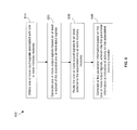
- FIG. 5 is a flow diagram illustrating the operation of the monitoring systems 204 a , 204 b of FIGS. 2A and 2B , according to other embodiments.
- one or more parameters on a memory module of one or more memory modules are monitored.
- corresponding parameter information is transmitted away from the respective memory module to a device that is external to the respective memory module.
- the parameter information may be aggregated for display in a manner indicative of the level of memory module activity on the respective memory module.
- FIG. 6 is a flow diagram illustrating the operation of the monitoring systems 204 a and 204 b of FIGS. 2A and 2B , and of the monitoring unit 104 of FIG. 1 , according to some other embodiments.
- one or more input signals associated with one or more memory modules are detected.
- one or more output signals are generated based on at least a subset of the detected one or more input signals.
- the one or more output signals are routed to an area external to the associated one or more memory modules.
- a first parameter information based on the one or more output signals is generated, wherein the first parameter information is indicative of activity on the associated one or more memory modules.
Abstract
Description
Claims (20)
Priority Applications (3)
| Application Number | Priority Date | Filing Date | Title |
|---|---|---|---|
| US12/764,051 US9020781B2 (en) | 2009-12-11 | 2010-04-20 | Monitoring memory module parameters in high performance computers |
| CN201180030150.1A CN102959638B (en) | 2010-04-20 | 2011-04-19 | For method associated with one or more memory modules, equipment and system |
| PCT/US2011/033082 WO2011146193A1 (en) | 2010-04-20 | 2011-04-19 | Monitoring memory module parameters in high performance computers |
Applications Claiming Priority (2)
| Application Number | Priority Date | Filing Date | Title |
|---|---|---|---|
| US12/636,673 US9026401B2 (en) | 2009-12-11 | 2009-12-11 | Monitoring memory module parameters in high performance computers |
| US12/764,051 US9020781B2 (en) | 2009-12-11 | 2010-04-20 | Monitoring memory module parameters in high performance computers |
Related Parent Applications (1)
| Application Number | Title | Priority Date | Filing Date |
|---|---|---|---|
| US12/636,673 Continuation-In-Part US9026401B2 (en) | 2009-12-11 | 2009-12-11 | Monitoring memory module parameters in high performance computers |
Publications (2)
| Publication Number | Publication Date |
|---|---|
| US20110144951A1 US20110144951A1 (en) | 2011-06-16 |
| US9020781B2 true US9020781B2 (en) | 2015-04-28 |
Family
ID=44991981
Family Applications (1)
| Application Number | Title | Priority Date | Filing Date |
|---|---|---|---|
| US12/764,051 Active 2030-10-21 US9020781B2 (en) | 2009-12-11 | 2010-04-20 | Monitoring memory module parameters in high performance computers |
Country Status (3)
| Country | Link |
|---|---|
| US (1) | US9020781B2 (en) |
| CN (1) | CN102959638B (en) |
| WO (1) | WO2011146193A1 (en) |
Cited By (1)
| Publication number | Priority date | Publication date | Assignee | Title |
|---|---|---|---|---|
| US20150115868A1 (en) * | 2013-10-30 | 2015-04-30 | Samsung Electronics Co., Ltd. | Energy harvest and storage system and multi-sensor module |
Families Citing this family (4)
| Publication number | Priority date | Publication date | Assignee | Title |
|---|---|---|---|---|
| EP2811410B1 (en) * | 2012-12-21 | 2018-05-30 | Huawei Technologies Co., Ltd. | Monitoring record management method and device |
| TWI492049B (en) | 2013-02-06 | 2015-07-11 | Ibm | Memory module status indication method and apparatus |
| CN109324938A (en) * | 2018-10-08 | 2019-02-12 | 郑州云海信息技术有限公司 | A kind of method of batch detection RAM information |
| CN110955569B (en) * | 2019-11-26 | 2021-10-01 | 英业达科技有限公司 | Method, system, medium, and apparatus for testing dual inline memory module |
Citations (9)
| Publication number | Priority date | Publication date | Assignee | Title |
|---|---|---|---|---|
| US6480946B1 (en) | 1998-11-09 | 2002-11-12 | Mitsubishi Denki Kabushiki Kaisha | Memory system for synchronized and high speed data transfer |
| US20040007326A1 (en) * | 2002-07-12 | 2004-01-15 | Roche Gregory A. | Wafer probe for measuring plasma and surface characteristics in plasma processing enviroments |
| US6930554B2 (en) * | 2003-07-18 | 2005-08-16 | Freescale Semiconductor, Inc. | Variable gain low noise amplifier and method |
| US20060045168A1 (en) * | 2004-08-31 | 2006-03-02 | Pny Technologies, Inc. | Electronic module with built-in temperature display |
| US20060239095A1 (en) | 2005-03-30 | 2006-10-26 | Jun Shi | Memory device communication using system memory bus |
| US20070047378A1 (en) | 2005-02-14 | 2007-03-01 | Wolford Barry J | Method And Apparatus For Obtaining Memory Status Information Cross-Reference To Related Applications |
| US20070211548A1 (en) | 2005-03-30 | 2007-09-13 | Sandeep Jain | Temperature determination and communication for multiple devices of a memory module |
| US20080267258A1 (en) * | 2007-04-30 | 2008-10-30 | Qimonda North America Corp. | System and method for monitoring temperature in a multiple die package |
| US20090024790A1 (en) | 2006-07-31 | 2009-01-22 | Suresh Natarajan Rajan | Memory circuit system and method |
Family Cites Families (1)
| Publication number | Priority date | Publication date | Assignee | Title |
|---|---|---|---|---|
| CN101578614A (en) * | 2007-01-30 | 2009-11-11 | 松下电器产业株式会社 | Nonvolatile storage device, nonvolatile storage system, and access device |
-
2010
- 2010-04-20 US US12/764,051 patent/US9020781B2/en active Active
-
2011
- 2011-04-19 CN CN201180030150.1A patent/CN102959638B/en active Active
- 2011-04-19 WO PCT/US2011/033082 patent/WO2011146193A1/en active Application Filing
Patent Citations (9)
| Publication number | Priority date | Publication date | Assignee | Title |
|---|---|---|---|---|
| US6480946B1 (en) | 1998-11-09 | 2002-11-12 | Mitsubishi Denki Kabushiki Kaisha | Memory system for synchronized and high speed data transfer |
| US20040007326A1 (en) * | 2002-07-12 | 2004-01-15 | Roche Gregory A. | Wafer probe for measuring plasma and surface characteristics in plasma processing enviroments |
| US6930554B2 (en) * | 2003-07-18 | 2005-08-16 | Freescale Semiconductor, Inc. | Variable gain low noise amplifier and method |
| US20060045168A1 (en) * | 2004-08-31 | 2006-03-02 | Pny Technologies, Inc. | Electronic module with built-in temperature display |
| US20070047378A1 (en) | 2005-02-14 | 2007-03-01 | Wolford Barry J | Method And Apparatus For Obtaining Memory Status Information Cross-Reference To Related Applications |
| US20060239095A1 (en) | 2005-03-30 | 2006-10-26 | Jun Shi | Memory device communication using system memory bus |
| US20070211548A1 (en) | 2005-03-30 | 2007-09-13 | Sandeep Jain | Temperature determination and communication for multiple devices of a memory module |
| US20090024790A1 (en) | 2006-07-31 | 2009-01-22 | Suresh Natarajan Rajan | Memory circuit system and method |
| US20080267258A1 (en) * | 2007-04-30 | 2008-10-30 | Qimonda North America Corp. | System and method for monitoring temperature in a multiple die package |
Non-Patent Citations (2)
| Title |
|---|
| PCT/US11/33082, PCT International Search Report dated Jul. 20, 2011. |
| PCT/US11/33082, PCT Written Opinion of the International Search Authority dated Jul. 20, 2011. |
Cited By (2)
| Publication number | Priority date | Publication date | Assignee | Title |
|---|---|---|---|---|
| US20150115868A1 (en) * | 2013-10-30 | 2015-04-30 | Samsung Electronics Co., Ltd. | Energy harvest and storage system and multi-sensor module |
| US10193377B2 (en) * | 2013-10-30 | 2019-01-29 | Samsung Electronics Co., Ltd. | Semiconductor energy harvest and storage system for charging an energy storage device and powering a controller and multi-sensor memory module |
Also Published As
| Publication number | Publication date |
|---|---|
| US20110144951A1 (en) | 2011-06-16 |
| WO2011146193A1 (en) | 2011-11-24 |
| CN102959638A (en) | 2013-03-06 |
| CN102959638B (en) | 2018-06-29 |
Similar Documents
| Publication | Publication Date | Title |
|---|---|---|
| US9020781B2 (en) | Monitoring memory module parameters in high performance computers | |
| US9270062B2 (en) | Electronic device and connector detection circuit thereof | |
| US8732366B2 (en) | Method to configure serial communications and device thereof | |
| US20140245080A1 (en) | Interface detection circuit | |
| US10088514B2 (en) | Orientation indicator with pin signal alteration | |
| US8081730B2 (en) | Monitoring device for connectors | |
| US20090116823A1 (en) | Fan speed control device | |
| US20100037079A1 (en) | Built-in system power management circuit and motherboard with thereof | |
| US9026401B2 (en) | Monitoring memory module parameters in high performance computers | |
| US20190361832A1 (en) | Bus system and detection method thereof | |
| US8225023B2 (en) | Indicator control apparatus | |
| US20120124395A1 (en) | Computer power supply | |
| US20040246675A1 (en) | Instrumentation console for personal computers | |
| US20060039408A1 (en) | Budget sensor bus | |
| US8374820B2 (en) | Test circuit for network interface | |
| US6457089B1 (en) | Microprocessor bus structure | |
| US20210173464A1 (en) | System for visualizing power signal sequence | |
| US9360524B2 (en) | Testing system for serial interface | |
| US10901935B2 (en) | IC, bus system and control method thereof | |
| US8634186B2 (en) | Non-volatile memory controller cable arrangement | |
| TWI413905B (en) | Apparatus for testing usb ports | |
| US8719558B2 (en) | Distinguishing circuit | |
| JP2003223373A (en) | Data transmitting/receiving buffer | |
| US20160259359A1 (en) | Voltage level control circuit and semiconductor system | |
| US20220353490A1 (en) | Video accuracy verification |
Legal Events
| Date | Code | Title | Description |
|---|---|---|---|
| AS | Assignment |
Owner name: CORSAIR MEMORY, INC., CALIFORNIA Free format text: ASSIGNMENT OF ASSIGNORS INTEREST;ASSIGNORS:LIEBERMAN, DONALD A;SOLVIN, DANIEL R;REEL/FRAME:024372/0833 Effective date: 20100426 |
|
| AS | Assignment |
Owner name: BANK OF AMERICA, N.A., AS AGENT, ILLINOIS Free format text: NOTICE OF GRANT OF SECURITY INTEREST IN PATENTS;ASSIGNORS:CORSAIR MEMORY, INC.;CORSAIR COMPONENTS, INC.;REEL/FRAME:033341/0422 Effective date: 20140711 |
|
| STCF | Information on status: patent grant |
Free format text: PATENTED CASE |
|
| AS | Assignment |
Owner name: MACQUARIE CAPITAL FUNDING LLC, AS COLLATERAL AGENT, NEW YORK Free format text: FIRST LIEN INTELLECTUAL PROPERTY SECURITY AGREEMENT;ASSIGNOR:CORSAIR MEMORY, INC.;REEL/FRAME:043967/0980 Effective date: 20170828 Owner name: MACQUARIE CAPITAL FUNDING LLC, AS COLLATERAL AGENT, NEW YORK Free format text: SECOND LIEN INTELLECTUAL PROPERTY SECURITY AGREEMENT;ASSIGNOR:CORSAIR MEMORY, INC.;REEL/FRAME:043714/0171 Effective date: 20170828 Owner name: MACQUARIE CAPITAL FUNDING LLC, AS COLLATERAL AGENT Free format text: SECOND LIEN INTELLECTUAL PROPERTY SECURITY AGREEMENT;ASSIGNOR:CORSAIR MEMORY, INC.;REEL/FRAME:043714/0171 Effective date: 20170828 Owner name: MACQUARIE CAPITAL FUNDING LLC, AS COLLATERAL AGENT Free format text: FIRST LIEN INTELLECTUAL PROPERTY SECURITY AGREEMENT;ASSIGNOR:CORSAIR MEMORY, INC.;REEL/FRAME:043967/0980 Effective date: 20170828 |
|
| AS | Assignment |
Owner name: CORSAIR COMPONENTS, INC., CALIFORNIA Free format text: RELEASE BY SECURED PARTY;ASSIGNOR:BANK OF AMERICA, N.A.;REEL/FRAME:043462/0205 Effective date: 20170828 Owner name: CORSAIR MEMORY, INC., CALIFORNIA Free format text: RELEASE BY SECURED PARTY;ASSIGNOR:BANK OF AMERICA, N.A.;REEL/FRAME:043462/0205 Effective date: 20170828 |
|
| MAFP | Maintenance fee payment |
Free format text: PAYMENT OF MAINTENANCE FEE, 4TH YR, SMALL ENTITY (ORIGINAL EVENT CODE: M2551) Year of fee payment: 4 |
|
| AS | Assignment |
Owner name: CORSAIR MEMORY INC., CALIFORNIA Free format text: TERMINATION AND RELEASE OF SECOND LIEN SECURITY INTEREST IN INTELLECTUAL PROPERTY RECORDED AT REEL 043714, FRAME 0171;ASSIGNOR:MACQUARIE CAPITAL FUNDING LLC;REEL/FRAME:053706/0930 Effective date: 20200904 Owner name: ORIGIN PC, LLC, CALIFORNIA Free format text: TERMINATION AND RELEASE OF SECOND LIEN SECURITY INTEREST IN INTELLECTUAL PROPERTY RECORDED AT REEL 043714, FRAME 0171;ASSIGNOR:MACQUARIE CAPITAL FUNDING LLC;REEL/FRAME:053706/0930 Effective date: 20200904 |
|
| AS | Assignment |
Owner name: BANK OF AMERICA, N.A., AS ADMINISTRATIVE AGENT, NORTH CAROLINA Free format text: NOTICE OF GRANT OF SECURITY INTEREST IN PATENTS;ASSIGNOR:CORSAIR MEMORY, INC.;REEL/FRAME:057407/0001 Effective date: 20210903 |
|
| AS | Assignment |
Owner name: ORIGIN PC, LLC, CALIFORNIA Free format text: TERMINATION AND RELEASE OF FIRST LIEN SECURITY INTEREST IN INTELLECTUAL PROPERTY;ASSIGNOR:MACQUARIE CAPITAL FUNDING LLC;REEL/FRAME:057424/0357 Effective date: 20210903 Owner name: CORSAIR MEMORY, INC., CALIFORNIA Free format text: TERMINATION AND RELEASE OF FIRST LIEN SECURITY INTEREST IN INTELLECTUAL PROPERTY;ASSIGNOR:MACQUARIE CAPITAL FUNDING LLC;REEL/FRAME:057424/0357 Effective date: 20210903 |
|
| MAFP | Maintenance fee payment |
Free format text: PAYMENT OF MAINTENANCE FEE, 8TH YR, SMALL ENTITY (ORIGINAL EVENT CODE: M2552); ENTITY STATUS OF PATENT OWNER: SMALL ENTITY Year of fee payment: 8 |