US9019238B2 - Object-sensing device - Google Patents
Object-sensing device Download PDFInfo
- Publication number
- US9019238B2 US9019238B2 US12/914,888 US91488810A US9019238B2 US 9019238 B2 US9019238 B2 US 9019238B2 US 91488810 A US91488810 A US 91488810A US 9019238 B2 US9019238 B2 US 9019238B2
- Authority
- US
- United States
- Prior art keywords
- radiation
- waveguide
- receiving element
- display device
- radiation receiving
- Prior art date
- Legal status (The legal status is an assumption and is not a legal conclusion. Google has not performed a legal analysis and makes no representation as to the accuracy of the status listed.)
- Expired - Fee Related, expires
Links
Images


Classifications
-
- G—PHYSICS
- G06—COMPUTING; CALCULATING OR COUNTING
- G06F—ELECTRIC DIGITAL DATA PROCESSING
- G06F3/00—Input arrangements for transferring data to be processed into a form capable of being handled by the computer; Output arrangements for transferring data from processing unit to output unit, e.g. interface arrangements
- G06F3/01—Input arrangements or combined input and output arrangements for interaction between user and computer
- G06F3/03—Arrangements for converting the position or the displacement of a member into a coded form
- G06F3/041—Digitisers, e.g. for touch screens or touch pads, characterised by the transducing means
- G06F3/0412—Digitisers structurally integrated in a display
-
- G—PHYSICS
- G06—COMPUTING; CALCULATING OR COUNTING
- G06F—ELECTRIC DIGITAL DATA PROCESSING
- G06F3/00—Input arrangements for transferring data to be processed into a form capable of being handled by the computer; Output arrangements for transferring data from processing unit to output unit, e.g. interface arrangements
- G06F3/01—Input arrangements or combined input and output arrangements for interaction between user and computer
- G06F3/03—Arrangements for converting the position or the displacement of a member into a coded form
- G06F3/041—Digitisers, e.g. for touch screens or touch pads, characterised by the transducing means
- G06F3/042—Digitisers, e.g. for touch screens or touch pads, characterised by the transducing means by opto-electronic means
- G06F3/0421—Digitisers, e.g. for touch screens or touch pads, characterised by the transducing means by opto-electronic means by interrupting or reflecting a light beam, e.g. optical touch-screen
-
- G—PHYSICS
- G06—COMPUTING; CALCULATING OR COUNTING
- G06F—ELECTRIC DIGITAL DATA PROCESSING
- G06F2203/00—Indexing scheme relating to G06F3/00 - G06F3/048
- G06F2203/041—Indexing scheme relating to G06F3/041 - G06F3/045
- G06F2203/04109—FTIR in optical digitiser, i.e. touch detection by frustrating the total internal reflection within an optical waveguide due to changes of optical properties or deformation at the touch location
Definitions
- the present invention refers generally to an object-sensing device and more particularly to an object-sensing (e.g., touch-sensing) display device.
- object-sensing e.g., touch-sensing
- An object-sensing device is a device capable of sensing the presence of an object, and sometimes determines the location of the object on the device. Incorporation of object-sensing capability into display devices is becoming increasingly desirable, as it allows the display device itself to also be used as a user input device, eliminating the need for cumbersome components such as keyboards, keypads, and mouse.
- a user can, for example, touch images of buttons on the display to make a selection or type a word.
- Object-sensing display devices can be useful for applications such as automatic telling machines (ATMs), mobile/cellular phones, and personal digital assistants (PDAs).
- ATMs automatic telling machines
- PDAs personal digital assistants
- a resistive-type touch sensing display device senses a current change in response to the touch.
- a surface-wave-type touch sensing display device senses a supersonic change in response to the touch.
- a radiation-sensing-type display device typically includes a radiation emitting element and a radiation receiving element and senses a change in the intensity of the radiation when an object is present compared to when no object is present.
- the radiation-sensing-type display device is advantageous because of its large object-sensing area, it is desirable to lower its manufacturing cost.
- the invention is an object-sensing display device that includes a waveguide and a substrate holding a liquid crystal layer, wherein radiation propagates through the waveguide via total internal reflection.
- a radiation emitting element is positioned along a radiation input surface of the waveguide, and a radiation receiving element is positioned to receive radiation exiting the waveguide.
- the invention is an object-sensing device that includes a waveguide that transmits radiation via total internal reflection from a first end to a second end, a radiation emitting element positioned at a first end of the waveguide, and a radiation receiving element positioned at a second end of the waveguide. Edges of the waveguide that do not correspond to the first end or the second end are free of radiation emitting element and radiation receiving element.
- the invention is an object-sensing display device that incorporates the above object-sensing device.
- the display device includes a common electrode formed on the waveguide, and a thin film transistor array substrate having pixel electrodes formed thereon disposed on the common electrode with a liquid crystal layer between the pixel electrodes and the common electrode.
- the invention is a computer-readable medium containing instructions for executing a method for determining the location of an object on a surface in an x-y plane.
- the method entails obtaining data regarding intensity of radiation at various points along an x-direction, and using a rate of intensity change in the x-direction to determine the y-coordinate of the object.
- the point of minimum intensity along the x-direction is used to determine the x-coordinate of the object.
- FIG. 1 is a cross-sectional view of an object-sensing display device in accordance with one embodiment of the invention.
- FIG. 2 is a perspective view of the object-sensing display device.
- FIG. 3 is a plan view of an object-sensing device capable of being used with a display device.
- FIG. 4 shows the radiation intensity as a function of x when an object is at a location A of the object-sensing device.
- FIG. 5 shows the radiation intensity as a function of x when an object is at a location B on the object-sensing device.
- FIG. 6 shows the radiation intensity as a function of x under three scenarios: when an object at a location C, when an object at a location D, and when an object at a location E on the object-sensing device.
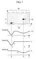
- FIGS. 7 and 8 show the radiation intensity as a function of x in a “multi-touch” situation where multiple objects are on the object-sensing device at the same time.
- FIGS. 9-12 , 14 , 15 , and 17 show different embodiments of the object-sensing display device.
- FIG. 13 is a plan view of a waveguide in an exemplary object-sensing display device.
- FIG. 16 is a cross-sectional view of a radiation receiving element formed on the waveguide via a thin film transistor fabrication process.
- FIG. 17 is a cross-sectional view of an embodiment of the object-sensing display device.
- FIG. 18 is a cross-sectional view of an embodiment of the object-sensing display device.
- a first element “holding” a second element means the first element is playing a part in keeping the second element in its position such that removal of the first element would cause the second element to fall apart, spill, leak, or otherwise get displaced.
- FIG. 1 is a cross-sectional view of an object-sensing display device 10 according to a first embodiment of the invention.
- the object-sensing display device 10 includes a waveguide 100 and a thin film transistor (TFT) substrate 300 holding a liquid crystal layer 200 .
- the waveguide 100 receives radiation at a radiation input surface 103 , which is optically coupled to a radiation emitting element 110 .
- the received radiation travels through the waveguide 100 (as shown by an arrow 101 ) and reaches a radiation receiving element 120 positioned on the other side of the waveguide 100 .
- An upper polarizer 401 and a lower polarizer 402 are placed on the outermost surfaces of the waveguide 100 and the TFT substrate 300 , respectively.
- a subsidiary layer 130 is formed on an internal surface of the waveguide 100 to reduce radiation leakage.
- a color filter layer 301 and a light blocking member 302 are formed on the TFT substrate 300 .
- the TFT substrate 300 includes circuitry connecting gate electrodes, source electrodes, drain electrodes, storage electrodes, and pixel electrodes (none of which are shown).
- the pixel electrode may be formed on the color filter layer 301 and the light blocking member 302 .
- a common electrode ( 270 ) is formed on the subsidiary layer 130 .
- the radiation emitted by the radiation emitting element 110 which may be infrared radiation, travels through the waveguide 100 via total internal reflection.
- the subsidiary layer 130 includes a material having a low index of refraction to help the radiation stay in the waveguide 100 .
- Scattered radiation 102 is shown in FIG. 1 .
- the radiation receiving element 120 receives a baseline level of radiation emitted by the radiation emitting element 110 when no object is present at the surface of the display device 10 .
- frustrated total internal reflection causes some radiation to escape the waveguide 100 before reaching the radiation receiving element 120 , thereby lowering the level of radiation that reaches the radiation receiving element 120 .
- the radiation receiving element 120 uses the amount by which the radiation level is reduced to determine the presence and the location of the object 600 , as will be explained in more detail below.
- the embodiment of FIG. 1 is slimmer, lighter, and less expensive to manufacture because there is one fewer substrate used.
- the waveguide 100 serves a dual function: one as a waveguide for object detection, and another as a liquid crystal display panel that is holding the liquid crystal layer 200 .
- FIG. 2 is a perspective view of the object-sensing display device 10 .
- the radiation emitting elements 110 positioned along the radiation input surface 103 of the waveguide 100 , may be a series of infrared light emitting diodes (LEDs) or lamps mounted on a PCB.
- the wavelength of the emitted radiation may be between about 850 nm and about 980 nm.
- the radiation emitting elements 110 contact the radiation input surface 103 such that there is no air gap between the radiation emitting elements 110 and the waveguide 100 .
- PMMA polymethyl methacrylate
- the thickness of the waveguide 100 may be about 0.1-10 mm.
- the radiation receiving elements 120 may be a series of infrared-sensitive photodiodes, charge-coupled devices (CCDs), phototransistors, image cameras, etc. mounted on another PCB.
- a computer is coupled to the PCB supporting the radiation receiving elements 120 to receive the amounts of radiation sensed by each of the radiation receiving elements 120 and determine the location of the object 600 (see FIG. 1 ).
- FIG. 3 is a plan view of the object-sensing portion of the object-sensing display device 10 .
- the number of radiation emitting elements 110 is equal to the number of radiation receiving elements 120 . More specifically, the radiation emitting elements 110 a , 110 b , 110 c , etc. correspond with radiation receiving elements 120 a , 120 b , 120 c , etc.
- the emitter-receiver pairs are scanned line by line at approximately 60 Hz. For example, the radiation emitting element 110 a and the radiation receiving element 120 a will be turned on, then the radiation emitting element 110 b and the radiation receiving element 120 b will be turned on, then 110 c and 120 c , etc.
- one of the radiation receiving elements 120 receives a reduced level of radiation.
- This detection of sub-baseline radiation level triggers a group of radiation receiving elements 120 around the radiation receiving element 120 i to turn on simultaneously.
- the specific “group” of radiation receiving elements 120 that turn on may be determined based on which radiation receiving elements 120 fall inside the critical angle ⁇ .
- the radiation is at its peak intensity at ⁇ /2, and falls off to about 50% of the peak intensity at the outer limits of the angle.
- the “group” may be all the radiation receiving elements 120 .
- the “group” that simultaneously gets turned on may be a predetermined number of radiation receiving elements 120 to the left and to the right of the radiation receiving element 120 i .
- This invention is not limited to which and how many radiation receiving elements 120 are turned on in response to the initial detection of object presence.
- FIGS. 4-8 illustrate the method by which the location of the object is determined using the signals from the radiation receiving elements 120 .
- a group of radiation receiving elements 120 around the radiation receiving element 120 i is turned on to get a “profile” of the radiation intensity.
- the direction in which the radiation receiving elements 120 are aligned is referred to as the x-direction.
- the direction from a radiation receiving element to a corresponding radiation emitting element 110 is referred to as the y-direction.
- FIGS. 3-8 are not limited to being used with a display device or a liquid crystal display, and may be adapted to non-display applications that incorporate object-sensing capability.
- the object-sensing device without the display portion would include the waveguide 100 , the radiation emitting element 110 , the radiation receiving element 120 , and the computer for carrying out the location determination.
- FIG. 4 shows the intensity as a function of x when an object is at a location A of the object-sensing device.
- the flat portion of the plot indicates the baseline intensity, which is the radiation intensity detected by the radiation receiving elements 120 when no object is present.
- the radiation receiving elements 120 that are farther away from the radiation receiving element 120 1 are less affected by the presence of the object than the elements 120 that are closer. By looking for the stationary point of the parabola, the x-coordinate of the object can be determined.
- FIG. 5 shows the intensity as a function of x when an object is at a location B of the object-sensing device.
- the location B has the same y-coordinate as the location A of FIG. 4 , but is shifted in the x-direction.
- a radiation receiving element 120 2 detects the lowest level of radiation, and the stationary point of the parabola is at x 2 .
- FIG. 6 shows the intensity as a function of x under three scenarios: when an object at a location C, when an object at a location D, and when an object at a location E of the object-sensing device.
- the three locations are all at the same x-coordinate but have different y-coordinates. As shown, the three locations produce parabolas with stationary points at the same point along the x-direction. However, the slopes of the parabolas differ depending on the y-coordinate. Due to the fact that radiation spreads in the manner shown in FIG. 3 , an object that is closer to the radiation emitting element 110 blocks a greater portion of the total width of the radiation cone.
- the intensity at the stationary point is not as low as in the case where the object is closer to the radiation receiving element 120 .
- the closer an object is to the radiation emitting element 110 the shallower the “dip” of the parabola will be and the less steep the slope will be.
- location E which is closer to the radiation receiving element 120
- the stationary point of the parabola is at a lower intensity than at locations C or D and the slope of the parabola is also steeper.
- FIGS. 7 and 8 illustrate a “multi-touch” situation where multiple objects are on the object-sensing device at the same time.
- FIG. 7 there are two objects, one at location F and another at location G. Since the two locations have different x-coordinates and y-coordinates, the two parabolas have stationary points at different points along the x-direction and their slopes are also different.
- the computer that determines the object locations separates the parabolas out as shown to determine the x- and y-coordinates of each object.
- FIG. 8 illustrates a “multi-touch” situation where two objects are at the same x-coordinate, hence producing overlapping parabolas.
- the two parabolas have their stationary points at the same x-coordinate but have different slopes. Since the object that is closer to the radiation emitting element 110 will generate a wider parabola than the object that is farther from the radiation emitting element 110 , the overlapped parabola will show two different slopes. Based on the two different slopes, the computer that is determining the object locations will separate out the two parabolas. Using the two parabolas, the x- and y-coordinates for both objects can be determined.
- FIGS. 9-17 show different embodiments of the object-sensing display device 10 .
- FIGS. 9 , 10 , and 11 show embodiments where the radiation receiving elements 120 are positioned across the waveguide 100 from the radiation emitting elements 110 , as in the embodiment of FIG. 1 . In these embodiments, the radiation receiving elements 120 detect the amount of radiation that is totally internally reflected through the waveguide 100 .
- the method for determining the location of an object that is described in reference to FIGS. 4-8 may be applied to the embodiments of FIGS. 9 , 10 , and 11 .
- FIG. 9 is a cross-sectional view of a second embodiment of the object-sensing display device 10 .
- the embodiment of FIG. 9 is similar to the embodiment of FIG. 1 except that the color filter layer 301 and the light blocking member 302 are formed on the waveguide 100 instead of the TFT substrate 300 .
- FIG. 10 is a cross-sectional view of a third embodiment of the object-sensing display device 10 .
- this embodiment has a waveguide on top of a liquid crystal display that has two substrates. More specifically, an intermediate substrate 500 and the TFT substrate 300 are holding the liquid crystal layer 200 in this embodiment.
- the waveguide 100 is placed on top of the liquid crystal device but does not play a role in holding the liquid crystal layer 200 .
- the color filters 301 and the light blocking members 302 are formed on the intermediate substrate 500 .
- the subsidiary layer 130 is formed on the internal surface of the waveguide 100 to ensure total internal reflection.
- the upper polarizer 401 is formed between the subsidiary layer 130 and the intermediate substrate 500 .
- a common electrode (not shown) is formed on the color filters 301 and the light blocking member 302 .
- FIG. 11 is a cross-sectional view of a fourth embodiment of the object-sensing display device 10 .
- This embodiment is similar to the embodiment of FIG. 2 , except that the radiation receiving elements 120 are formed directly on the waveguide 100 through a photolithography and fabrication process instead of being mounted on a PCB and being optically coupled to a waveguide surface.
- FIGS. 12-17 have radiation receiving elements 120 positioned on a surface of the waveguide 100 that contacts the radiation input surface 103 .
- these surfaces are perpendicular to the radiation input surface 103 .
- the radiation receiving elements 120 detect the amount of scattered radiation 102 .
- the radiation receiving element 120 of FIGS. 12-17 may be a photodiode, a photo-transistor, CCD, etc. and may be formed via a thin film transistor fabrication process. When thin film process is used to form the radiation receiving element 120 , photolithography and thin film deposition techniques may be used.
- the radiation receiving element 120 is preferably formed in a light blocking area so that it will not decrease the aperture ratio of the device. By forming the radiation receiving element 120 through thin film process, manufacturing cost may be decreased compared to the embodiments where they are mounted on a PCB and coupled to the waveguide 100 .
- Disposing the radiation receiving element 120 on the waveguide 100 may result in a smaller object-sensing display device 10 compared to disposing the radiation receiving elements 120 on a side of the waveguide 100 (as in the embodiments of FIGS. 1 and 9 - 11 ).
- FIG. 12 is a cross-sectional view of a fifth embodiment of the object-sensing display device 10 .
- This embodiment differs from the embodiment of FIG. 1 in that the radiation receiving elements 120 are positioned on the subsidiary layer 130 instead of the surface of the waveguide 100 opposite the radiation input surface 103 . Instead of measuring the amount of radiation that is totally internally reflected to be transmitted across the waveguide 100 as in the embodiment of FIG. 1 , the radiation receiving elements 120 receive the scattered radiation 102 .
- the radiation that reaches the radiation receiving elements 120 is radiation that leaves the waveguide 100 via the bottom surface.
- FIG. 13 is a plan view of the waveguide 100 in an exemplary object-sensing display device 10 .
- This view shows the radiation receiving elements 120 arranged on the waveguide 100 in a two-dimensional, matrix configuration.
- the number of radiation receiving elements 120 may be the same as or less than the number of pixels on the display device.
- the radiation emitting element 110 includes a radiation source 111 , a radiation guide member 112 , and a microlens (not shown) for directing the radiation in a desired direction.
- the radiation sources 111 are at the corners of the waveguide 100 with the radiation guide member 112 extending between them.
- the radiation source 111 may be any device (light emitting diode, lamp, etc.) that emits wavelengths such as infrared rays of between about 850 nm and about 980 nm.
- the radiation emitted by the radiation sources 111 propagates in the y-direction via total internal reflection as shown in the coordinates by being distributed by the radiation guide member 112 .
- the radiation travels across the waveguide 100 , causing the radiation receiving elements 120 to receive a certain low (or zero) level of radiation in the absence of an object to cause scattering.
- the scattered radiation is sensed by the radiation receiving element 120 at the location that corresponds to where the scattering occurred.
- the radiation receiving element 120 upon detecting radiation, forwards the intensity reading to a computer (not shown).
- scanning may be performed on a row-by-row basis as in the embodiment of FIG. 3 .
- row a will be activated, then row b, and then row c, from one end of the waveguide 100 to the other at a preselected frequency (e.g., 60 Hz).
- a group of radiation receiving elements 120 around the row i may be activated to determine exactly which radiation receiving element 120 received the maximum amount of scattered radiation.
- the “group” may be, for example, two rows above and below row i although this invention is not limited to any specific “group.”
- the x- and y-coordinates can be determined based on the identification of the radiation receiving element 120 that received the maximum radiation.
- the invention allows the location of multiple objects on the display surface to be detected simultaneously. This allows a user to make a selection by touching two points on an image simultaneously, providing more flexibility to the manner in which he can input information.
- FIG. 14 is a cross-sectional view of a sixth embodiment of the object-sensing display device 10 .
- the sixth embodiment is similar to the fifth embodiment shown in FIG. 12 except that there are three substrate layers instead of two, and the radiation receiving elements 120 are formed on the intermediate substrate 500 . More specifically, this embodiment has a waveguide on top of a liquid crystal display that has two substrates. An intermediate substrate 500 and the TFT substrate 300 hold the liquid crystal layer 200 , and the waveguide 100 is disposed on top of the intermediate substrate 500 .
- the radiation receiving elements 120 are disposed on a color filter 301 , preferably in a two-dimensional configuration (e.g., the matrix configuration of FIG. 13 ).
- the radiation receiving elements 120 receive the radiation that is scattered out of the waveguide 100 by the object(s) 600 , and the radiation receiving elements 120 that receive the most radiation correspond to the location of the object(s) 600 . Theoretically, as many objects 600 as the number of radiation receiving elements 120 may be detected simultaneously.
- FIG. 15 is a cross-sectional view of an embodiment of the object-sensing display device 10 that shows details of the radiation emitting element 110 .
- the radiation emitting element 110 includes the radiation source(s) 111 , the radiation guide member 112 , and the micro lens 113 between the radiation source and the waveguide 100 .
- the waveguide 100 and the TFT substrate 300 sandwich the liquid crystal layer 200 , and the radiation sensing elements 120 are disposed between the subsidiary layer 130 and the liquid crystal layer 200 .
- the radiation from the radiation emitting element 110 propagates through the waveguide 100 in the y-direction by total internal reflection.
- the radiation gets scattered, causing the radiation receiving element 120 to receive a level of radiation above the baseline level when no object is present.
- the increased level of radiation is turned into a signal and forwarded to the computer (not shown) for processing and location determination.
- FIG. 16 is a cross-sectional view of a radiation receiving element 120 formed on the waveguide 100 via a thin film transistor fabrication process.
- a band pass filter may be formed to remove radiation of predetermined ranges.
- an active layer 120 - a is formed using a material such as Si or Si—Ge.
- An ohmic contact layer (not shown) may be formed on the active layer 120 - a , and a radiation receiving source electrode 120 - s and drain electrode 120 - d are formed on the active layer 120 - a .
- the radiation receiving source electrode 120 - s and the radiation receiving drain electrode 120 - d are covered with an insulation layer 120 -I, and a radiation receiving gate electrode 120 - g is formed.
- Each of the radiation receiving elements 120 shown in FIG. 14 may have the cross section shown in FIG. 16 .
- FIG. 17 is a cross-sectional view of an embodiment of the object-sensing display device 10 . This embodiment is similar to the embodiment of FIG. 15 with the exception of an absorption polarizer 140 .
- FIG. 18 is also a cross-sectional view of an embodiment of the object-sensing display device 10 .
- the radiation receiving element 120 is disposed under the waveguide 100 and along with an edge of the waveguide 100 . That is, the radiation receiving elements 120 are aligned in one direction along with one edge.
- this embodiment is similar to the embodiment of FIG. 11 , the difference between two embodiments is that radiation receiving element 120 is disposed under the waveguide 100 in this embodiment.
- the gap is not essential and according to embodiments, they may contact each other without a gap.
Abstract
Description
Claims (24)
Applications Claiming Priority (2)
| Application Number | Priority Date | Filing Date | Title |
|---|---|---|---|
| KR10-2010-0026311 | 2010-03-24 | ||
| KR1020100026311A KR101749266B1 (en) | 2010-03-24 | 2010-03-24 | Touch sensing display device and cumputer-readable medium |
Publications (2)
| Publication Number | Publication Date |
|---|---|
| US20110234537A1 US20110234537A1 (en) | 2011-09-29 |
| US9019238B2 true US9019238B2 (en) | 2015-04-28 |
Family
ID=43728797
Family Applications (1)
| Application Number | Title | Priority Date | Filing Date |
|---|---|---|---|
| US12/914,888 Expired - Fee Related US9019238B2 (en) | 2010-03-24 | 2010-10-28 | Object-sensing device |
Country Status (5)
| Country | Link |
|---|---|
| US (1) | US9019238B2 (en) |
| EP (1) | EP2369451B1 (en) |
| JP (1) | JP5856373B2 (en) |
| KR (1) | KR101749266B1 (en) |
| CN (1) | CN102200855B (en) |
Cited By (2)
| Publication number | Priority date | Publication date | Assignee | Title |
|---|---|---|---|---|
| US20140098065A1 (en) * | 2012-10-04 | 2014-04-10 | Corning Incorporated | Touch screen systems and methods for sensing touch screen displacement |
| US20170131845A1 (en) * | 2015-11-05 | 2017-05-11 | Infilm Optoelectronic Inc. | Guide light plate touch device using imaging unit |
Families Citing this family (52)
| Publication number | Priority date | Publication date | Assignee | Title |
|---|---|---|---|---|
| SG124249A1 (en) | 2001-12-07 | 2006-08-30 | Sumitomo Chemical Co | New polymer and polymer light-emitting device using the same |
| SE533704C2 (en) | 2008-12-05 | 2010-12-07 | Flatfrog Lab Ab | Touch sensitive apparatus and method for operating the same |
| US8963886B2 (en) * | 2011-07-13 | 2015-02-24 | Flatfrog Laboratories Ab | Touch-sensing display panel |
| US8884900B2 (en) | 2011-07-13 | 2014-11-11 | Flatfrog Laboratories Ab | Touch-sensing display apparatus and electronic device therewith |
| US9019240B2 (en) * | 2011-09-29 | 2015-04-28 | Qualcomm Mems Technologies, Inc. | Optical touch device with pixilated light-turning features |
| WO2013081894A1 (en) | 2011-11-28 | 2013-06-06 | Corning Incorporated | Optical touch-screen systems and methods using a planar transparent sheet |
| CN104160366A (en) | 2011-11-28 | 2014-11-19 | 康宁股份有限公司 | Robust optical touch-screen systems and methods using a planar transparent sheet |
| JP5593006B2 (en) * | 2012-03-11 | 2014-09-17 | ネオノード インコーポレイテッド | Optical touch screen using total internal reflection |
| KR101386147B1 (en) * | 2012-04-05 | 2014-04-17 | 최대규 | Infrared touch screen devices |
| US9880653B2 (en) | 2012-04-30 | 2018-01-30 | Corning Incorporated | Pressure-sensing touch system utilizing total-internal reflection |
| ITMI20120813A1 (en) * | 2012-05-11 | 2013-11-12 | Fond Istituto Italiano Di Tecnologia | TACTILE DETECTION DEVICE AND PROCESS. |
| US10168835B2 (en) | 2012-05-23 | 2019-01-01 | Flatfrog Laboratories Ab | Spatial resolution in touch displays |
| WO2013176615A2 (en) | 2012-05-23 | 2013-11-28 | Flatfrog Laboratories Ab | Touch-sensitive apparatus with improved spatial resolution |
| EP2852879A4 (en) | 2012-05-23 | 2016-02-17 | Flatfrog Lab Ab | Touch-sensitive apparatus with improved spatial resolution |
| CN103453449B (en) * | 2012-06-04 | 2015-12-02 | 原相科技股份有限公司 | Light guide module and relative photo arrangement for detecting thereof |
| US9405382B2 (en) * | 2012-07-24 | 2016-08-02 | Rapt Ip Limited | Augmented optical waveguide for use in an optical touch sensitive device |
| US9041690B2 (en) | 2012-08-06 | 2015-05-26 | Qualcomm Mems Technologies, Inc. | Channel waveguide system for sensing touch and/or gesture |
| US9285623B2 (en) * | 2012-10-04 | 2016-03-15 | Corning Incorporated | Touch screen systems with interface layer |
| US9557846B2 (en) | 2012-10-04 | 2017-01-31 | Corning Incorporated | Pressure-sensing touch system utilizing optical and capacitive systems |
| US20140118270A1 (en) * | 2012-10-26 | 2014-05-01 | Qualcomm Incorporated | System and method for providing infrared gesture interaction on a display |
| WO2014112913A1 (en) * | 2013-01-16 | 2014-07-24 | Flatfrog Laboratories Ab | Touch-sensing display panel |
| US10019113B2 (en) | 2013-04-11 | 2018-07-10 | Flatfrog Laboratories Ab | Tomographic processing for touch detection |
| TWI486845B (en) * | 2013-07-01 | 2015-06-01 | Infilm Optoelectronic Inc | The use of diffracted light within the total reflection of the light guide plate touch device |
| WO2015005847A1 (en) | 2013-07-12 | 2015-01-15 | Flatfrog Laboratories Ab | Partial detect mode |
| CN105531653A (en) * | 2013-07-19 | 2016-04-27 | 惠普发展公司,有限责任合伙企业 | Light guide panel including diffraction gratings |
| JP6197492B2 (en) * | 2013-08-29 | 2017-09-20 | コニカミノルタ株式会社 | Touch panel input device, touch panel input device control method, and touch panel input device control program |
| WO2015076731A1 (en) | 2013-11-22 | 2015-05-28 | Flatfrog Laboratories Ab | A touch sensitive apparatus with improved spatial resolution |
| US10146376B2 (en) | 2014-01-16 | 2018-12-04 | Flatfrog Laboratories Ab | Light coupling in TIR-based optical touch systems |
| US10126882B2 (en) | 2014-01-16 | 2018-11-13 | Flatfrog Laboratories Ab | TIR-based optical touch systems of projection-type |
| US9921688B2 (en) * | 2014-03-04 | 2018-03-20 | Qualcomm Incorporated | Large area interactive display screen |
| WO2015199602A1 (en) | 2014-06-27 | 2015-12-30 | Flatfrog Laboratories Ab | Detection of surface contamination |
| FR3025052B1 (en) * | 2014-08-19 | 2017-12-15 | Isorg | DEVICE FOR DETECTING ELECTROMAGNETIC RADIATION IN ORGANIC MATERIALS |
| US9898114B2 (en) | 2014-12-23 | 2018-02-20 | Intel Corporation | Electroactive privacy layer of a display device |
| EP3250993B1 (en) | 2015-01-28 | 2019-09-04 | FlatFrog Laboratories AB | Dynamic touch quarantine frames |
| US10318074B2 (en) | 2015-01-30 | 2019-06-11 | Flatfrog Laboratories Ab | Touch-sensing OLED display with tilted emitters |
| EP3537269A1 (en) | 2015-02-09 | 2019-09-11 | FlatFrog Laboratories AB | Optical touch system |
| WO2016140612A1 (en) | 2015-03-02 | 2016-09-09 | Flatfrog Laboratories Ab | Optical component for light coupling |
| GB2541361A (en) * | 2015-07-01 | 2017-02-22 | Joseph Edwards Thomas | Method and apparatus to enable smartphones and computer tablet devices to communicate with interactive devices |
| KR101731905B1 (en) | 2015-07-16 | 2017-05-24 | 장지훈 | Train speed improving system and method therefor |
| EP4075246A1 (en) | 2015-12-09 | 2022-10-19 | FlatFrog Laboratories AB | Stylus for optical touch system |
| KR102511622B1 (en) * | 2016-06-09 | 2023-03-17 | 엘지전자 주식회사 | Refrigerator |
| WO2018096430A1 (en) | 2016-11-24 | 2018-05-31 | Flatfrog Laboratories Ab | Automatic optimisation of touch signal |
| HUE059960T2 (en) | 2016-12-07 | 2023-01-28 | Flatfrog Lab Ab | A curved touch device |
| US10963104B2 (en) | 2017-02-06 | 2021-03-30 | Flatfrog Laboratories Ab | Optical coupling in touch-sensing systems |
| EP3602257A4 (en) | 2017-03-22 | 2021-01-13 | Flatfrog Laboratories | Eraser for touch displays |
| CN110663015A (en) | 2017-03-28 | 2020-01-07 | 平蛙实验室股份公司 | Touch sensitive device and method for assembly |
| CN106873284B (en) * | 2017-04-10 | 2019-10-29 | 京东方科技集团股份有限公司 | A kind of display device and its control method |
| CN111052058B (en) | 2017-09-01 | 2023-10-20 | 平蛙实验室股份公司 | Improved optical component |
| US11567610B2 (en) | 2018-03-05 | 2023-01-31 | Flatfrog Laboratories Ab | Detection line broadening |
| US11943563B2 (en) | 2019-01-25 | 2024-03-26 | FlatFrog Laboratories, AB | Videoconferencing terminal and method of operating the same |
| KR20220131982A (en) | 2020-02-10 | 2022-09-29 | 플라트프로그 라보라토리즈 에이비 | Enhanced touch-sensing device |
| US11520183B2 (en) * | 2020-12-29 | 2022-12-06 | Tpk Touch Solutions (Xiamen) Inc. | Touch front light module and touch display device |
Citations (31)
| Publication number | Priority date | Publication date | Assignee | Title |
|---|---|---|---|---|
| US20020067348A1 (en) | 1999-12-02 | 2002-06-06 | Masters Timothy E. | Apparatus and method to improve resolution of infrared touch systems |
| JP2005235174A (en) | 2004-02-19 | 2005-09-02 | Au Optronics Corp | Touch panel unit and detecting method for position on display panel |
| JP2005316517A (en) | 2004-04-26 | 2005-11-10 | Idec Izumi Corp | Optical touch panel |
| US6972753B1 (en) | 1998-10-02 | 2005-12-06 | Semiconductor Energy Laboratory Co., Ltd. | Touch panel, display device provided with touch panel and electronic equipment provided with display device |
| US20060114237A1 (en) | 2004-11-17 | 2006-06-01 | Crockett Timothy W | Method and system for providing a frustrated total internal reflection touch interface |
| JP2006155616A (en) | 2004-11-30 | 2006-06-15 | Agilent Technol Inc | Touch input system using light guide |
| US7098592B2 (en) * | 2003-12-10 | 2006-08-29 | Sanyo Electric Co., Ltd. | Electroluminescent display device |
| US20060227120A1 (en) * | 2005-03-28 | 2006-10-12 | Adam Eikman | Photonic touch screen apparatus and method of use |
| JP2006318512A (en) | 1998-10-02 | 2006-11-24 | Semiconductor Energy Lab Co Ltd | Information terminal equipment |
| WO2006134552A2 (en) | 2005-06-14 | 2006-12-21 | Koninklijke Philips Electronics N.V. | Flexible displays and user input means therefor |
| JP2007042093A (en) | 2005-07-29 | 2007-02-15 | Avago Technologies Fiber Ip (Singapore) Pte Ltd | Method and system for detecting selection by touch |
| WO2007083883A1 (en) * | 2006-01-19 | 2007-07-26 | Nexio Co., Ltd | Refined coordinate detection method and error correction method for touch panel |
| US20080029691A1 (en) | 2006-08-03 | 2008-02-07 | Han Jefferson Y | Multi-touch sensing display through frustrated total internal reflection |
| US20080030484A1 (en) * | 2006-08-07 | 2008-02-07 | Samsung Electronics Co., Ltd. | Dual liquid crystal display having touch screen |
| WO2008066004A1 (en) | 2006-11-30 | 2008-06-05 | Sega Corporation | Position inputting apparatus |
| KR20080060127A (en) | 2006-12-26 | 2008-07-01 | 엘지디스플레이 주식회사 | Organic light emitting diode panel and touch screen system comprising the same |
| JP2008181411A (en) | 2007-01-25 | 2008-08-07 | Nitto Denko Corp | Optical waveguide for touch panel |
| US20080285310A1 (en) | 2007-05-16 | 2008-11-20 | Aylward Peter T | Elongated illuminators configuration for lcd displays |
| US20080284925A1 (en) | 2006-08-03 | 2008-11-20 | Han Jefferson Y | Multi-touch sensing through frustrated total internal reflection |
| JP2008293114A (en) | 2007-05-22 | 2008-12-04 | Citizen Electronics Co Ltd | Touch panel with illumination, and display device provided with the touch panel |
| US20090128508A1 (en) | 2007-11-19 | 2009-05-21 | Min Ho Sohn | Multi touch flat display module |
| KR20090057542A (en) | 2007-12-03 | 2009-06-08 | 엘지디스플레이 주식회사 | Touch panel display apparatus |
| CN101510134A (en) | 2008-02-14 | 2009-08-19 | 索尼株式会社 | Display apparatus and image pickup apparatus |
| JP2009187342A (en) | 2008-02-07 | 2009-08-20 | Seiko Epson Corp | Touch panel, electrooptical device, and electronic device |
| WO2010024008A1 (en) | 2008-08-29 | 2010-03-04 | シャープ株式会社 | Coordinate sensor, electronic device, display device, and light-receiving unit |
| US20100128006A1 (en) * | 2008-11-26 | 2010-05-27 | Nitto Denko Corporation | Optical waveguide and optical touch panel |
| US20100283763A1 (en) * | 2009-05-08 | 2010-11-11 | Samsung Electronics Co., Ltd. | Multi-sensing touch panel and display apparatus using the same |
| US20100302481A1 (en) * | 2009-06-01 | 2010-12-02 | Baum Alexandra | Absorbing wire grid polarizer |
| US20110043490A1 (en) * | 2009-08-21 | 2011-02-24 | Microsoft Corporation | Illuminator for touch- and object-sensitive display |
| US8013845B2 (en) * | 2005-12-30 | 2011-09-06 | Flatfrog Laboratories Ab | Optical touch pad with multilayer waveguide |
| US20110304586A1 (en) * | 2010-06-14 | 2011-12-15 | Yeh Chia-Jui | Infrared type handwriting input apparatus and scanning method |
Family Cites Families (3)
| Publication number | Priority date | Publication date | Assignee | Title |
|---|---|---|---|---|
| JPH1050124A (en) * | 1996-08-06 | 1998-02-20 | Seiko Epson Corp | Lighting system and liquid crystal display |
| JP2008300630A (en) * | 2007-05-31 | 2008-12-11 | Sharp Corp | Semiconductor device and manufacturing method thereof |
| JP4697552B2 (en) * | 2008-04-18 | 2011-06-08 | ソニー株式会社 | Image display device and driving method of image display device |
-
2010
- 2010-03-24 KR KR1020100026311A patent/KR101749266B1/en active IP Right Grant
- 2010-10-28 US US12/914,888 patent/US9019238B2/en not_active Expired - Fee Related
-
2011
- 2011-01-13 JP JP2011004472A patent/JP5856373B2/en not_active Expired - Fee Related
- 2011-01-21 EP EP11151617.5A patent/EP2369451B1/en not_active Not-in-force
- 2011-02-23 CN CN201110043285.3A patent/CN102200855B/en not_active Expired - Fee Related
Patent Citations (36)
| Publication number | Priority date | Publication date | Assignee | Title |
|---|---|---|---|---|
| US6972753B1 (en) | 1998-10-02 | 2005-12-06 | Semiconductor Energy Laboratory Co., Ltd. | Touch panel, display device provided with touch panel and electronic equipment provided with display device |
| JP2006318512A (en) | 1998-10-02 | 2006-11-24 | Semiconductor Energy Lab Co Ltd | Information terminal equipment |
| JP2009110540A (en) | 1998-10-02 | 2009-05-21 | Semiconductor Energy Lab Co Ltd | Display equipped with touch panel and electronic appliance |
| US20020067348A1 (en) | 1999-12-02 | 2002-06-06 | Masters Timothy E. | Apparatus and method to improve resolution of infrared touch systems |
| US6429857B1 (en) | 1999-12-02 | 2002-08-06 | Elo Touchsystems, Inc. | Apparatus and method to improve resolution of infrared touch systems |
| US7098592B2 (en) * | 2003-12-10 | 2006-08-29 | Sanyo Electric Co., Ltd. | Electroluminescent display device |
| JP2005235174A (en) | 2004-02-19 | 2005-09-02 | Au Optronics Corp | Touch panel unit and detecting method for position on display panel |
| JP2005316517A (en) | 2004-04-26 | 2005-11-10 | Idec Izumi Corp | Optical touch panel |
| US20060114237A1 (en) | 2004-11-17 | 2006-06-01 | Crockett Timothy W | Method and system for providing a frustrated total internal reflection touch interface |
| JP2006155616A (en) | 2004-11-30 | 2006-06-15 | Agilent Technol Inc | Touch input system using light guide |
| US20060227120A1 (en) * | 2005-03-28 | 2006-10-12 | Adam Eikman | Photonic touch screen apparatus and method of use |
| WO2006134552A2 (en) | 2005-06-14 | 2006-12-21 | Koninklijke Philips Electronics N.V. | Flexible displays and user input means therefor |
| JP2007042093A (en) | 2005-07-29 | 2007-02-15 | Avago Technologies Fiber Ip (Singapore) Pte Ltd | Method and system for detecting selection by touch |
| US8013845B2 (en) * | 2005-12-30 | 2011-09-06 | Flatfrog Laboratories Ab | Optical touch pad with multilayer waveguide |
| WO2007083883A1 (en) * | 2006-01-19 | 2007-07-26 | Nexio Co., Ltd | Refined coordinate detection method and error correction method for touch panel |
| US8009152B2 (en) * | 2006-01-19 | 2011-08-30 | Nexio Co., Ltd. | Refined coordinate detection method and error correction method for touch panel |
| US20080029691A1 (en) | 2006-08-03 | 2008-02-07 | Han Jefferson Y | Multi-touch sensing display through frustrated total internal reflection |
| US20080284925A1 (en) | 2006-08-03 | 2008-11-20 | Han Jefferson Y | Multi-touch sensing through frustrated total internal reflection |
| US20080030484A1 (en) * | 2006-08-07 | 2008-02-07 | Samsung Electronics Co., Ltd. | Dual liquid crystal display having touch screen |
| WO2008066004A1 (en) | 2006-11-30 | 2008-06-05 | Sega Corporation | Position inputting apparatus |
| KR20080060127A (en) | 2006-12-26 | 2008-07-01 | 엘지디스플레이 주식회사 | Organic light emitting diode panel and touch screen system comprising the same |
| JP2008181411A (en) | 2007-01-25 | 2008-08-07 | Nitto Denko Corp | Optical waveguide for touch panel |
| US20080285310A1 (en) | 2007-05-16 | 2008-11-20 | Aylward Peter T | Elongated illuminators configuration for lcd displays |
| JP2008293114A (en) | 2007-05-22 | 2008-12-04 | Citizen Electronics Co Ltd | Touch panel with illumination, and display device provided with the touch panel |
| US20090128508A1 (en) | 2007-11-19 | 2009-05-21 | Min Ho Sohn | Multi touch flat display module |
| KR20090051613A (en) | 2007-11-19 | 2009-05-22 | 엘지디스플레이 주식회사 | Multi touch flat display module |
| KR20090057542A (en) | 2007-12-03 | 2009-06-08 | 엘지디스플레이 주식회사 | Touch panel display apparatus |
| JP2009187342A (en) | 2008-02-07 | 2009-08-20 | Seiko Epson Corp | Touch panel, electrooptical device, and electronic device |
| CN101510134A (en) | 2008-02-14 | 2009-08-19 | 索尼株式会社 | Display apparatus and image pickup apparatus |
| US20090207145A1 (en) * | 2008-02-14 | 2009-08-20 | Sony Corporation | Display apparatus and image pickup apparatus |
| WO2010024008A1 (en) | 2008-08-29 | 2010-03-04 | シャープ株式会社 | Coordinate sensor, electronic device, display device, and light-receiving unit |
| US20100128006A1 (en) * | 2008-11-26 | 2010-05-27 | Nitto Denko Corporation | Optical waveguide and optical touch panel |
| US20100283763A1 (en) * | 2009-05-08 | 2010-11-11 | Samsung Electronics Co., Ltd. | Multi-sensing touch panel and display apparatus using the same |
| US20100302481A1 (en) * | 2009-06-01 | 2010-12-02 | Baum Alexandra | Absorbing wire grid polarizer |
| US20110043490A1 (en) * | 2009-08-21 | 2011-02-24 | Microsoft Corporation | Illuminator for touch- and object-sensitive display |
| US20110304586A1 (en) * | 2010-06-14 | 2011-12-15 | Yeh Chia-Jui | Infrared type handwriting input apparatus and scanning method |
Non-Patent Citations (1)
| Title |
|---|
| European Search Report corresponding to European Patent Application No. 11151617.5, Feb. 11, 2015, 9 pages. |
Cited By (3)
| Publication number | Priority date | Publication date | Assignee | Title |
|---|---|---|---|---|
| US20140098065A1 (en) * | 2012-10-04 | 2014-04-10 | Corning Incorporated | Touch screen systems and methods for sensing touch screen displacement |
| US9619084B2 (en) * | 2012-10-04 | 2017-04-11 | Corning Incorporated | Touch screen systems and methods for sensing touch screen displacement |
| US20170131845A1 (en) * | 2015-11-05 | 2017-05-11 | Infilm Optoelectronic Inc. | Guide light plate touch device using imaging unit |
Also Published As
| Publication number | Publication date |
|---|---|
| US20110234537A1 (en) | 2011-09-29 |
| EP2369451A2 (en) | 2011-09-28 |
| CN102200855B (en) | 2016-07-06 |
| KR20110107128A (en) | 2011-09-30 |
| JP2011204223A (en) | 2011-10-13 |
| EP2369451A3 (en) | 2015-03-11 |
| EP2369451B1 (en) | 2017-05-17 |
| CN102200855A (en) | 2011-09-28 |
| KR101749266B1 (en) | 2017-07-04 |
| JP5856373B2 (en) | 2016-02-09 |
Similar Documents
| Publication | Publication Date | Title |
|---|---|---|
| US9019238B2 (en) | Object-sensing device | |
| WO2017118067A1 (en) | Optical-type fingerprint identification display screen and display device | |
| TWI451311B (en) | Touch-sensing display device | |
| WO2018171178A1 (en) | Fingerprint identification device, control method, touch display panel and touch display device | |
| US8854336B2 (en) | Light guide module, optical touch module, and method of increasing a signal to noise ratio of an optical touch module | |
| US9347833B2 (en) | Infrared touch and hover system using time-sequential measurements | |
| CN102081483B (en) | Optical sensing module | |
| TWI522869B (en) | Optical touch display apparatus | |
| US20100289755A1 (en) | Touch-Sensing Liquid Crystal Display | |
| US11361578B2 (en) | Method for detecting biometric information, biometric sensor, and display apparatus | |
| JP5025551B2 (en) | Touch panel | |
| US20120062817A1 (en) | Liquid crystal display device | |
| US9477349B2 (en) | Touch panel and touch display device having the same | |
| TWI496058B (en) | Optical touchscreen | |
| US20110261300A1 (en) | Area sensor and display device having area sensor | |
| US10956702B2 (en) | Apparatus for recognizing a fingerprint, and display device | |
| US20150205442A1 (en) | Optical touch screen | |
| US20110148818A1 (en) | Optical touch display apparatus | |
| US9086318B1 (en) | Transmissive barrier in a transmissive sheet | |
| US20120262422A1 (en) | Optical touch module and method thereof | |
| US20110102371A1 (en) | Optical Touch Panel | |
| CN110008869B (en) | Display panel and display device | |
| US20180307377A1 (en) | Touch substrate and touch display device | |
| TWI435249B (en) | Touch sense module and touch display using the same | |
| TWI622936B (en) | Optical fingerprint detection device supporting multi-finger detection |
Legal Events
| Date | Code | Title | Description |
|---|---|---|---|
| AS | Assignment |
Owner name: SAMSUNG ELECTRONICS CO., LTD., KOREA, REPUBLIC OF Free format text: ASSIGNMENT OF ASSIGNORS INTEREST;ASSIGNORS:KIM, JIN-HWAN;HWANG, SEONG-MO;NAM, SEUNG-HO;AND OTHERS;REEL/FRAME:025214/0867 Effective date: 20101025 |
|
| AS | Assignment |
Owner name: SAMSUNG DISPLAY CO., LTD., KOREA, REPUBLIC OF Free format text: ASSIGNMENT OF ASSIGNORS INTEREST;ASSIGNOR:SAMSUNG ELECTRONICS CO., LTD.;REEL/FRAME:028999/0685 Effective date: 20120904 |
|
| FEPP | Fee payment procedure |
Free format text: PAYOR NUMBER ASSIGNED (ORIGINAL EVENT CODE: ASPN); ENTITY STATUS OF PATENT OWNER: LARGE ENTITY |
|
| STCF | Information on status: patent grant |
Free format text: PATENTED CASE |
|
| MAFP | Maintenance fee payment |
Free format text: PAYMENT OF MAINTENANCE FEE, 4TH YEAR, LARGE ENTITY (ORIGINAL EVENT CODE: M1551); ENTITY STATUS OF PATENT OWNER: LARGE ENTITY Year of fee payment: 4 |
|
| FEPP | Fee payment procedure |
Free format text: MAINTENANCE FEE REMINDER MAILED (ORIGINAL EVENT CODE: REM.); ENTITY STATUS OF PATENT OWNER: LARGE ENTITY |
|
| LAPS | Lapse for failure to pay maintenance fees |
Free format text: PATENT EXPIRED FOR FAILURE TO PAY MAINTENANCE FEES (ORIGINAL EVENT CODE: EXP.); ENTITY STATUS OF PATENT OWNER: LARGE ENTITY |
|
| STCH | Information on status: patent discontinuation |
Free format text: PATENT EXPIRED DUE TO NONPAYMENT OF MAINTENANCE FEES UNDER 37 CFR 1.362 |
|
| FP | Lapsed due to failure to pay maintenance fee |
Effective date: 20230428 |