US9004366B2 - Wireless devices including printed integrated circuitry and methods for manufacturing and using the same - Google Patents
Wireless devices including printed integrated circuitry and methods for manufacturing and using the same Download PDFInfo
- Publication number
- US9004366B2 US9004366B2 US12/249,707 US24970708A US9004366B2 US 9004366 B2 US9004366 B2 US 9004366B2 US 24970708 A US24970708 A US 24970708A US 9004366 B2 US9004366 B2 US 9004366B2
- Authority
- US
- United States
- Prior art keywords
- substrate
- antenna
- layer
- stock
- inductor
- Prior art date
- Legal status (The legal status is an assumption and is not a legal conclusion. Google has not performed a legal analysis and makes no representation as to the accuracy of the status listed.)
- Expired - Fee Related, expires
Links
Images


Classifications
-
- G—PHYSICS
- G06—COMPUTING; CALCULATING OR COUNTING
- G06K—GRAPHICAL DATA READING; PRESENTATION OF DATA; RECORD CARRIERS; HANDLING RECORD CARRIERS
- G06K19/00—Record carriers for use with machines and with at least a part designed to carry digital markings
- G06K19/06—Record carriers for use with machines and with at least a part designed to carry digital markings characterised by the kind of the digital marking, e.g. shape, nature, code
- G06K19/067—Record carriers with conductive marks, printed circuits or semiconductor circuit elements, e.g. credit or identity cards also with resonating or responding marks without active components
- G06K19/07—Record carriers with conductive marks, printed circuits or semiconductor circuit elements, e.g. credit or identity cards also with resonating or responding marks without active components with integrated circuit chips
- G06K19/077—Constructional details, e.g. mounting of circuits in the carrier
- G06K19/07749—Constructional details, e.g. mounting of circuits in the carrier the record carrier being capable of non-contact communication, e.g. constructional details of the antenna of a non-contact smart card
- G06K19/0775—Constructional details, e.g. mounting of circuits in the carrier the record carrier being capable of non-contact communication, e.g. constructional details of the antenna of a non-contact smart card arrangements for connecting the integrated circuit to the antenna
- G06K19/07752—Constructional details, e.g. mounting of circuits in the carrier the record carrier being capable of non-contact communication, e.g. constructional details of the antenna of a non-contact smart card arrangements for connecting the integrated circuit to the antenna using an interposer
-
- Y—GENERAL TAGGING OF NEW TECHNOLOGICAL DEVELOPMENTS; GENERAL TAGGING OF CROSS-SECTIONAL TECHNOLOGIES SPANNING OVER SEVERAL SECTIONS OF THE IPC; TECHNICAL SUBJECTS COVERED BY FORMER USPC CROSS-REFERENCE ART COLLECTIONS [XRACs] AND DIGESTS
- Y10—TECHNICAL SUBJECTS COVERED BY FORMER USPC
- Y10T—TECHNICAL SUBJECTS COVERED BY FORMER US CLASSIFICATION
- Y10T29/00—Metal working
- Y10T29/49—Method of mechanical manufacture
- Y10T29/49002—Electrical device making
- Y10T29/49117—Conductor or circuit manufacturing
- Y10T29/49124—On flat or curved insulated base, e.g., printed circuit, etc.
Definitions
- the present invention generally relates to the field of sensors and electronic article surveillance (EAS), radio frequency (RF) and/or RF identification (RFID) tags and devices. More specifically, embodiments of the present invention pertain to tags/devices utilizing printed integrated circuitry with an attached antenna, typically EAS, RF and/or RFID tags and devices, and methods for their manufacturing and/or production. As a result, the present invention may provide a low-cost process for producing an RFID (or EAS) tag comprising printed integrated circuitry and an antenna.
- EAS electronic article surveillance
- RFID radio frequency
- RFID RF identification
- Remotely powered electronic devices and related systems are known.
- U.S. Pat. No. 5,099,227 issued to Geiszler et al. and entitled “Proximity Detecting Apparatus,” discloses a remotely powered device which uses electromagnetic coupling to derive power from a remote source, then uses both electromagnetic and electrostatic coupling to transmit stored data to a receiver, often collocated with the remote source.
- Such remotely powered communication devices are commonly known as radio frequency identification (“RFID”) tags.
- RFID radio frequency identification
- RFID tags and associated systems have numerous uses. For example, RFID tags are frequently used for personal identification in automated gate sentry applications, protecting secured buildings or areas. These tags often take the form of access control cards. Information stored on the RFID tag identifies the tag holder seeking access to the secured building or area. Older automated gate sentry applications generally require the person accessing the building to insert or swipe their identification card or tag into or through a reader for the system to read the information from the card or tag. Newer RFID tag systems allow the tag to be read at a short distance using radio frequency data transmission technology, thereby eliminating the need to insert or swipe an identification tag into or through a reader. Most typically, the user simply holds or places the tag near a base station, which is coupled to a security system securing the building or area.
- the base station transmits an excitation signal to the tag that powers circuitry contained on the tag.
- the circuitry in response to the excitation signal, communicates stored information from the tag to the base station, which receives and decodes the information.
- the information is then processed by the security system to determine if access is appropriate.
- RFID tags may be written (e.g., programmed and/or deactivated) remotely by an excitation signal, appropriately modulated in a predetermined manner.
- Some conventional RFID tags and systems use primarily electromagnetic coupling to remotely power the remote device and couple the remote device with an exciter system and a receiver system.
- the exciter system generates an electromagnetic excitation signal that powers up the device and causes the device to transmit a signal which may include stored information.
- the receiver receives the signal produced by the remote device.
- These conventional RFID tags are manufactured such that the integrated circuitry is manufactured separately from the antenna and/or inductor, and the two components are then physically and electrically connected. These components are manufactured separately, in part, due to the cost of manufacturing silicon wafers. It would be cost prohibitive to manufacture both components on a silicon wafer.
- the antenna and/or inductor is a simple structure and can be manufactured on a less expensive substrate using less expensive processing methods and joined to the integrated circuitry in a later manufacturing step.
- conventional RFID tags are formed by a process that includes dicing a wafer manufactured by conventional wafer-based processes into a plurality of die.
- a die is then placed onto an antenna or inductor carrier (which may contain an antenna, inductor coil or other conducting feature) in a chip-to-antenna attach process.
- the die can be attached to an intermediate carrier (or interposer) in a two-step chip-to-strap/strap-to-antenna attach process.
- a die 120 is attached to an interposer (or carrier) 140 .
- Electrical paths 130 and 132 from the die 120 to relatively larger and/or more widely distributed areas (e.g., 134 or 136 ) for attaching ends of the antenna are present in certain locations on the interposer 140 .
- This assembly may then be attached, as shown in FIG. 1B to a support film 150 containing inductor/antenna 152 .
- the assembly on the interposer 140 is sometimes known as a “strap.”
- This attach process may include various physical bonding techniques, such as gluing, as well as establishing electrical interconnection(s) via wire bonding, anisotropic conductive epoxy bonding, ultrasonics, bump-bonding or flip-chip approaches.
- the attach process often involves the use of heat, time, and/or UV exposure. Since the die 120 is usually made as small as possible ( ⁇ 1 mm 2 ) to reduce the cost per die, the pad elements for external electrical connections to the die 120 may be relatively small. This means that the placing operation should be of relatively high accuracy for high speed mechanical operation (e.g., placement to within 50 microns of a predetermined position is often required).
- the carriers generally contain electrical paths from the die to relatively larger and/or more widely distributed areas in other locations on the carrier to allow high-throughput, low resolution attachment operations such as crimping or conductive adhesive attach (somewhat functionally similar to a conventional strap, as compared to a pick-and-place and/or wire bonding based process for direct integration of a chip die to an inductor substrate).
- low resolution attach processes suitable for straps could be performed at costs near $0.003 or less, based on commercially available equipment and materials (e.g., a Mühlbauer TMA 6000 or similar apparatus).
- the carriers are then attached to an inductor/antenna 152 such that electrical connections are formed at such other locations.
- This carrier-based process may also have advantages for flip-chip or bump bonding approaches, where it may be more expensive or disadvantageous to implement the required stubs, bumps or other interconnect elements onto the larger inductor/carrier substrate 150 by conventional means (e.g., wire bonding).
- tags are a significant focus within the RFID industry.
- High RFID tag prices have been an obstacle against widespread adoption of RFID technology, especially in item-level retail applications and other low-cost, high-volume applications.
- One way of reducing tag costs is to develop a tag structure and process that incorporates (and preferably integrates) a less expensive substrate, a stable and effective antenna, RF front end devices, and high resolution patterned logic circuitry.
- Embodiments of the present invention relate to sensor, EAS, RF and/or RFID tags and devices having printed integrated circuitry and an affixed antenna and/or inductor, and methods for their manufacture and use.
- the device generally comprises: (a) printed integrated circuitry on a first substrate; (b) first and second pads on the first substrate and/or the printed integrated circuitry, electrically coupled to the printed integrated circuitry; and (c) an antenna and/or inductor on a second substrate comprising a conductive line having first and second ends thereon, the first and second ends being in electrical communication with the first and second pads, respectively.
- the method of manufacturing a device generally comprises the steps of: (1) forming printed integrated circuitry on a first substrate; (2) forming first and second pads electrically coupled to the printed integrated circuitry; (3) forming an antenna and/or inductor having first and second ends on a second substrate; and (4) attaching the first and second pads to first and second ends of the antenna and/or inductor.
- the method of manufacturing multiple devices generally comprises the steps of: (i) forming a plurality of printed integrated circuits on a first substrate stock to form a PIC stock; (ii) forming a plurality of antennas and/or inductors on a second substrate stock to form an antenna stock; and (iii) attaching the PIC stock to the antenna stock.
- the method of use generally comprises the steps of (i) causing or inducing a current in the present device sufficient for the device to radiate, reflect or modulate detectable electromagnetic signals; (ii) detecting the detectable electromagnetic radiation; and optionally, (iii) processing information conveyed by the detectable electromagnetic radiation.
- the method of use may further comprise the step of (iv) transporting or transmitting information from the present device (or sensor) back to a reading device.
- One potential approach to producing very low-cost RFID tags may use printing techniques in a roll- or sheet-fed process.
- Printing has potential cost advantages, since it can increase materials utilization (e.g., additive or semi-additive processing), combine deposition and patterning steps, and leverage low capital expenditures and operating costs for equipment.
- high throughput conventional printing processes can be adapted to flexible substrates (e.g., a plastic sheet or a metal foil), improving and/or expanding tag uses in a number of applications.
- the materials efficiency and additive processing approaches enables a lower cost per unit area of processed carriers (or die, when used), which enables low cost attach processing and/or integration of passive devices with the active circuitry.
- mask-less processes such as printing enable facile customization of RF devices, for example where each individual RF device is provided with a unique identification code and/or a unique response time delay with respect to a reader inquiry.
- circuitry can be printed in a manner that facilitates the attachment of the printed integrated circuitry to an antenna and/or inductor, the cost of the attach steps can be reduced significantly.
- Photovoltaic materials processing includes well-developed roll-to-roll manufacturing processes for inorganic semiconductors, dielectrics and other films on foils, sheets and/or other flexible substrates. Such processing provides an effective way to make RFID tags with equipment for processing display and photovoltaic devices (by itself or alternatively, in combination with printing steps that may enable a full manufacturing process without necessarily having a full tool and materials set developed for printed RFID tags).
- processing preferably includes spool-based and/or roll-to-roll printing processes, which should drive the manufacturing costs even lower due to the lower capital equipment costs, the high throughput (several hundreds of m 2 /hr), the increased efficiency in materials usage, and/or the decreased number of processing steps.
- the present invention advantageously provides a low cost sensors, electronic article surveillance (EAS), radio frequency (RF) and/or RF identification (RFID) tag and devices utilizing printed integrated circuitry with an attached antenna.
- EAS electronic article surveillance
- RF radio frequency
- RFID RF identification
- a low cost tag may be produced by directly printing or otherwise forming the circuitry on a substrate that is then relatively cheaply attached at relatively low accuracy to an antenna and/or inductor formed on a separate and potentially less expensive substrate.
- FIGS. 2A-2B show key steps in an exemplary process for manufacturing the present RFID tag/device involving attachment of a first carrier or substrate with printed integrated circuitry thereon to a second carrier or substrate containing an antenna thereon.
- FIGS. 3A-3B show cross-sectional views of the carrier with printed integrated circuitry thereon, attached to the antenna and/or inductor, with the printed integrated circuitry in a face-down and face-up orientation, respectively.
- FIGS. 4A-4B show front and back views of exemplary printed integrated circuit sheet stock, or PIC sheet stock, respectively
- FIG. 4C shows an exemplary alternate embodiment of PIC sheet stock.
- FIG. 4D shows front and side views of exemplary PIC roll stock.
- FIG. 6 shows an exemplary process utilizing pick-and-place processing.
- the terms “coupled to,” “connected to,” and “in communication with” mean direct or indirect coupling, connection or communication unless the context indicates otherwise. These terms are generally used interchangeably herein, but are generally given their art-recognized meanings. Also, for convenience and simplicity, the terms “RF,” “RFID,” and “identification” may be used interchangeably with respect to intended uses and/or functions of a device and/or tag, and the term “tag” or “device” may be used herein to refer to any RF and/or RFID sensor, tag and/or device.
- integrated circuitry and “printed integrated circuitry” refer to a unitary structure comprising a plurality of electrically active devices formed from a plurality of conductor, semiconductor and insulator thin films, but generally does not include discrete, mechanically attached components (such as die, wire bonds and leads, the carrier, or an antenna and/or inductor component), or materials having primarily an adhesive function.
- integrated circuitry and “printed integrated circuitry” refer to a unitary structure comprising a plurality of electrically active devices formed from a plurality of conductor, semiconductor and insulator thin films, but generally does not include discrete, mechanically attached components (such as die, wire bonds and leads, the carrier, or an antenna and/or inductor component), or materials having primarily an adhesive function.
- the term “antenna” may be used in a general context to refer to an antenna, an inductor, or an antenna and inductor.
- interposer”, “carrier” and/or “substrate” refer to a structure that may be used as a support for
- a “major surface” of a structure or feature is a surface defined at least in part by the largest axis of the structure or feature (e.g., if the structure is round and has a radius greater than its thickness, the radial surface[s] is/are the major surface of the structure).
- the present invention concerns devices having printed integrated circuitry and an attached antenna and/or inductor, typically including sensor, EAS, RF and/or RFID tags and devices, comprising (a) printed integrated circuitry on a first substrate; (b) first and second pads on the first substrate and/or the printed integrated circuitry, electrically coupled to the printed integrated circuitry; and (c) an antenna and/or inductor on a second substrate comprising a conductive line having first and second ends thereon, the first and second ends being in electrical communication with first and second pads, respectively.
- the substrate for the printed integrated circuit and/or the antenna and/or inductor may comprise a glass, a polyimide, a glass/polymer laminate, a high-temperature polymer, or a metal foil.
- the present invention concerns a method of manufacturing a device, generally comprising the steps of (1) forming a printed integrated circuit on a first substrate; (2) forming first and second pads electrically coupled to the printed integrated circuitry; (3) forming an antenna and/or inductor having first and second ends on a second substrate; and (4) attaching the first and second pads to the first and second ends of the antenna and/or inductor.
- the process used to attach of the pads of the integrated circuit to the corresponding pads on the antenna may comprise either gluing, bump-bonding, ultrasonic bonding, welding, soldering, and/or crimping.
- radio frequency identification devices generally comprising the steps of (A) forming a plurality of printed integrated circuits on a first substrate stock to form PIC stock; (B) forming a plurality of antennas and/or inductors on a second substrate stock to form antenna stock; (C) attaching the PIC stock to the antenna stock.
- the process used to attach the PIC stock to the antenna stock comprises a sheet-to-sheet process, a roll-to-roll process, a pick-and-place process, and/or a tape-and-reel process.
- Another aspect of the present invention concerns a method for using a radio frequency identification device generally comprising the steps of (i) causing or inducing a current in the present device sufficient for the device to radiate, reflect or modulate detectable electromagnetic signals; (ii) detecting the detectable electromagnetic radiation; and optionally, (iii) processing information conveyed by the detectable electromagnetic radiation.
- the method of use may further comprise the step of (iv) transporting or transmitting information from the present device (or sensor) back to a reading device.
- One aspect of the invention relates to an RF identification or other wireless device, comprising (a) printed integrated circuitry on a first substrate; and (b) first and second pads on the first substrate and/or the printed integrated circuitry, the first and second pads electrically coupled to the printed integrated circuitry; and (c) an antenna and/or inductor on a second substrate having a first and second ends, the first and second ends being in electrical communication with the first and second pads, respectively.
- the present invention provides a low-cost RFID (or EAS) tag (which may also include sensors, the signal modulation activities of which generally change as a result of certain external changes in the environment [e.g., temperature, conductivity of the structure or surface to which the sensor is attached, etc.], and active RF or wireless circuits and/or devices; e.g., tags with a battery on board) comprising a substrate (e.g., a carrier), an inductor/antenna, and an RF front end (or subset of an RF front end and logic circuit) fully capable of operating in accordance with modern wireless or RFID standards.
- a substrate e.g., a carrier
- an inductor/antenna e.g., an inductor/antenna
- an RF front end or subset of an RF front end and logic circuit
- the device 300 comprises a printed integrated circuit carrier (or PIC carrier) and an antenna and/or inductor carrier (or antenna carrier) attached together.
- the PIC carrier comprises a printed integrated circuit 302 formed on a first substrate 304 .
- the substrate has electrical paths/pads 306 and 307 in electrical communication with printed integrated circuit 302 .
- electrical paths 306 / 307 are formed at least in part on the substrate 304 and put on the printed integrated circuit 302 .
- electrical paths/pads 306 / 307 can be formed solely on printed integrated circuit 302 or on printed integrated circuit 302 and substrate 304 .
- the antenna carrier comprises substrate 310 and antenna and/or inductor 320 .
- the antenna and/or inductor comprise a bulk conductive layer 318 on a seed layer 312 .
- the antenna and/or inductor 320 can be printed on substrate 310 .
- the top (PIC side) of the PIC carrier is in contact with the top (antenna side) of the antenna carrier and first and second electrical paths/pads 306 / 307 are in contact with first and second antenna and/or inductor ends 314 / 316 , respectively.
- Adhesive 308 is used to affix electrical paths/pads 306 / 307 to the first and second antenna and/or inductor ends 314 / 316 .
- the bottom (substrate side) of the PIC carrier is in contact with the top of the antenna carrier.
- electrical paths/pads 326 / 327 are in contact with antenna and/or inductor 340 through holes in substrate 324 .
- substrate 324 comprises a metal which is selectively removed to form electrically conductive structures or pads that are isolated from each other.
- These other embodiments typically have an uppermost cap or passivation layer on the top of the PIC carrier.
- the pads may be formed from substrate 324 using a process similar to that used for forming antennas and/or inductors from a metal substrate (see e.g., U.S. patent application Ser. No. 11/452,108, filed on Jun. 12, 2006, the relevant portions of which are incorporated herein by reference).
- Substrate 304 for printed integrated circuit 302 may comprise any substrate capable of (i) providing physical support of the integrated circuitry formed thereon during formation thereof and for the antenna and/or inductor component attached thereto during attachment thereof, (ii) having integrated circuitry formed (preferably printed) thereon, and (iii) enabling electrical connections to be formed therethrough (i.e., so that signals can be transmitted between integrated circuitry formed on one substrate and the antenna and/or inductor formed on another substrate).
- the substrate may be flexible, inflexible or rigid.
- the substrate can be conductive (electrically active) or non-conductive (electrically inactive), electrically active referring to the properties of the substrate and not necessarily the interaction between the substrate and the printed integrated circuit.
- the substrate generally has a size that can be cost-effectively processed using conventional thin film processes and/or emerging or state-of-the-art printing processes, to produce low-cost RF circuits.
- Integrated circuitry can be formed on a flexible substrate such as polyimide, glass/polymer laminate, high temperature polymer, or metal foil, all of which may further include one or more barrier coats.
- Carriers manufactured from such substrates are generally substantially less expensive than a conventional silicon die of similar size. (However, a conventional RFID interposer typically has a size on the order of 1 cm 2 in area, as compared to a conventional silicon RFID die, which might be about 0.01 cm 2 or less in area.)
- anodized Al, Al/Cu, Cu, stainless steel or similar metal foil may serve as an interconnect, an electrode and/or a dielectric for large storage or IC resonance capacitors, inductors and/or as an electrode for a diode, MOS-device or FET, or as a write once read many (WORM), one-time programmable (OTP), deactivation or other memory storage element.
- WORM write once read many
- OTP one-time programmable
- a flexible material that may be adapted to withstand relatively high-temperature processing (e.g., a temperature of 300° C., 350° C., 400° C., 450° C. or more, up to a temperature of 500° C., 600° C., or 1000° C., generally without significant deterioration or decrease in its mechanical and/or electrical properties).
- relatively high-temperature processing e.g., a temperature of 300° C., 350° C., 400° C., 450° C. or more, up to a temperature of 500° C., 600° C., or 1000° C.
- the substrate may comprise a thin (50-200 micron) glass sheet or “slip,” a glass/polymer laminate, a high temperature polymer (e.g., a polyimide, a polyethersulfone, polyethylene naphthalate [PEN], polyether ether ketone [PEEK], etc.), or a metal foil such as aluminum, stainless steel or copper.
- a high temperature polymer e.g., a polyimide, a polyethersulfone, polyethylene naphthalate [PEN], polyether ether ketone [PEEK], etc.
- Exemplary thicknesses depend on the material used, but in general, range from about 25 ⁇ m to about 200 ⁇ m (e.g., from about 50 ⁇ m to about 100 ⁇ m).
- the substrate is conventionally cleaned and coated with a barrier material (such as silicon dioxide or aluminum oxide) before further processing.
- the coating step may comprise oxidation and/or anodization of a surface material of the substrate (e.g., a metal foil); deposition of a spin-on or fluid coated barrier film; sputtering, CVD, or spray coating a barrier material onto the substrate, or a combination of any of these processes (see, e.g., U.S. patent application Ser. No. 11/243,460, filed on Oct. 3, 2005, the relevant portion of which is incorporated herein by reference).
- the interposer comprises a metal sheet or foil
- the metal foil may be etched and/or cut as described in U.S. patent application Ser. No. 11/452,108, filed on Jun. 12, 2006, and U.S. Pat. Nos. 7,286,053 and 7,152,804; the relevant portions of each of which are incorporated herein by reference.
- Printed integrated circuit 302 may comprise integrated circuitry (e.g., complementary metal-oxide-semiconductor [CMOS] circuitry) and/or devices manufactured by printing one or more (preferably a plurality) of patterned layers on a substrate. Other layers may be printed or formed using other, more conventional techniques.
- CMOS complementary metal-oxide-semiconductor
- the integrated circuitry may comprise a gate metal layer; one or more semiconductor layers (e.g., a transistor channel layer, a source/drain terminal layer, and/or one or more lightly- or heavily-doped diode layers); a gate insulator layer between the gate metal layer and at least one of the semiconductor layers; one or more capacitor electrodes (each of which is generally capacitively coupled to another capacitor electrode, which may also be part of the integrated circuitry or which may be integrated with or part of the carrier or antenna/inductor layer); a plurality of metal conductors in electrical communication with the gate metal layer, the source and drain terminals, an uppermost and/or lowermost diode layer and/or an uppermost and/or lowermost capacitor electrode; and/or a dielectric layer between various metal conductors and/or semiconductor layer(s).
- semiconductor layers e.g., a transistor channel layer, a source/drain terminal layer, and/or one or more lightly- or heavily-doped diode layers
- a gate insulator layer between
- the integrated circuitry may further comprise one or more resistors, which may comprise a metal and/or lightly or heavily doped polysilicon.
- the integrated circuitry comprises a gate metal layer, a semiconductor layer (e.g., a transistor channel layer in contact with source/drain terminals, in the same layer or an overlying or underlying layer in contact with the channel layer), a gate insulator layer between the gate metal layer and the transistor channel layer, and a plurality of metal conductors in electrical communication with the gate metal layer and the source and drain terminals.
- Exemplary layers of integrated circuitry are described in greater detail in U.S. patent application Ser. Nos. 11/084,448, 11/203,563, and 11/243,460, respectively filed on Mar. 18, 2005, Aug. 11, 2005, and Oct. 3, 2005, the relevant portions of each of which are incorporated herein by reference.
- Substrate 310 for antenna and/or inductor 320 may comprise any substrate capable of (i) providing physical support of the antenna and/or inductor formed thereon during formation thereof and for the PIC carrier component attached thereto during attachment thereof, (ii) having the antenna and/or inductor formed (preferably printed) thereon, and (iii) enabling electrical connections to be formed therethrough (i.e., so that signals can be transmitted between integrated circuitry formed on one substrate and the antenna and/or inductor formed on another substrate).
- the substrate may be flexible, inflexible or rigid.
- the substrate can be conductive (electrically active) or non-conductive (electrically inactive), electrically active referring to the properties of the substrate and not the interaction between the substrate and the antenna and/or inductor.
- the antenna and/or inductor can be formed on the same materials as the printed integrated circuitry including polyimide, glass/polymer laminate, high temperature polymer, or metal foil, all of which may further include one or more barrier coats.
- the antenna and/or inductor may comprise the antenna, the inductor, or both, and may further comprise a capacitor electrode coupled thereto or integrated therewith (see, e.g., U.S. Pat. Nos. 7,152,804 and 7,286,053.
- the antenna and/or inductor may comprise one or more layers and/or coils. Further, the antenna and/or inductor may be formed on one or both sides of the substrate (see, e.g., U.S. patent application Ser. No. 11/749,114, filed May 15, 2007, the relevant portions of which are incorporated herein by reference).
- the antenna and/or inductor comprises a metal.
- the metal may comprise or consist essentially of aluminum, silver, gold, copper, palladium, titanium, chromium, molybdenum, tungsten, cobalt, nickel, platinum, zinc, iron, etc., or metal alloys thereof, preferably silver or gold, or an alloy thereof.
- the metal may comprise a foil of the aforementioned metals.
- the method of making a RFID and/or EAS device may further comprise the step of removing from the metal foil one or more portions of the metal located under (or opposite) electrically active integrated circuitry (e.g., transistors and diodes, but not necessarily a capacitor electrode or plate that includes a portion of the metal foil as an electrode or plate).
- electrically active integrated circuitry e.g., transistors and diodes, but not necessarily a capacitor electrode or plate that includes a portion of the metal foil as an electrode or plate.
- the inductor may function as a tuning inductor (see, e.g., U.S. Pat. No. 7,286,053, the relevant portions of which are incorporated herein by reference).
- the metal forming the antenna and inductor may not be continuous (i.e., it may contain an electrical disconnection), and a surveillance and/or identification device in accordance with the invention may comprise a first (e.g., outer) inductor coupled to a first capacitor plate, a second (e.g., inner) inductor coupled to a second capacitor plate, a dielectric film on the first (outer) inductor, the second (inner) inductor, and the first and second capacitor plates, the first dielectric film having openings therein exposing ends of each of the first and second (e.g., outer and inner) inductors.
- the capacitor plates may be linear or nonlinear, and/or the device may further comprise first and second nonlinear capacitor
- the present device may also further comprise a support and/or backing layer (not shown) on a surface of the first and/or second carrier 310 .
- the support and/or backing layer may be conventional, and are well known in the EAS and RFID arts (see, e.g., U.S. Pat. Appl. Publication No. 2002/0163434 and U.S. Pat. Nos. 5,841,350, 5,608,379 and 4,063,229).
- support and/or backing layers provide (1) an adhesive surface for subsequent attachment or placement of the tag/device onto an article to be tracked or monitored, and/or (2) some mechanical support for the tag/device.
- the present device may be affixed to the back of an identification label or price tag, and an adhesive coated or placed on the surface of the device opposite the identification label or price tag (optionally covered by a conventional release sheet until the label or tag is ready for use), to form a label or tag suitable for use in a conventional RFID system.
- the present invention concerns a method for making an identification device, comprising the steps of: (1) forming printed integrated circuitry on a first substrate; (2) forming first and second pads electrically coupled to the printed integrated circuitry; (3) forming an antenna and/or inductor having first and second ends on a second substrate; and (4) attaching the first and second pads to the first and second ends of the antenna and/or inductor.
- the present method provides a cost-effective method for manufacturing RFID devices.
- the ink used to produce the printed integrated circuitry may comprise a metal formulation for forming thin films.
- a metal formulation for forming thin films Such formulations enable the printing of a pure metal film using a metal precursor and reducing agent that generally does not leave substantially adverse levels of impurities and/or residues in the film.
- These ink formulation generally consists essentially of one or more Group 4, 5, 6, 7, 8, 9, 10, 11, or 12 metal salt(s) and/or metal complex(es), one or more solvents adapted to facilitate coating and/or printing of the formulation, and optionally, one or more additives that form gaseous or volatile byproducts upon reduction of the metal salt or metal complex to an elemental metal or alloy thereof.
- U.S. patent application Ser. No. 12/131,002 filed May 30, 2008, the relevant portions of which are incorporated herein by reference.
- FIG. 2A shows tag precursor (or printed integrated circuit) 200 , comprising substrate 232 and integrated circuitry 210 .
- integrated circuitry 210 is formed on a first major surface of carrier 232 .
- pads 234 and 236 are formed on the same surface of substrate 232 as integrated circuitry 210 , similar to the process for forming pads 134 and 136 in FIG. 1A .
- Pads 234 and 236 provide essentially the same function as pads 134 and 136 in FIG. 1A .
- FIG. 2B shows an antenna and/or inductor carrier 240 , comprising carrier 250 and an antenna and/or inductor 252 .
- the antenna and/or inductor 252 is formed on a first major surface of carrier 250 .
- the antenna and/or inductor 252 can be realized as an etched structure on a dielectric substrate, a plated structure, or a printed structure.
- holes or vias may be formed in the major surface of substrate 232 opposite that on which pads 234 and 236 and integrated circuitry 210 have been formed.
- FIG. 2A there are holes or vias through substrate 232 exposing a surface of pads 234 and 236 enabling electrical connection to a corresponding terminal of antenna/inductor 252 .
- one hole/via is provided per pad and each hole/via is in a location and has dimensions enabling facile contact between one terminal of antenna/inductor 252 and the corresponding pad, using a relatively high-throughput, low resolution attachment operation (as compared to a pick-and-place operation or wire bonding process for integration of a die 120 to an inductor substrate 140 ; see FIG. 1B ).
- inductor and/or antenna 252 (which may be affixed to or positioned on carrier 250 ) is then attached or affixed to substrate 232 such that electrical connections are formed between pads 234 and 236 and terminals of antenna/inductor 252 at locations corresponding to the holes or vias in substrate 232 .
- pads 234 and 236 are formed on the same surface of substrate 232 as integrated circuitry 210 , as above. However, the substrate 232 and carrier 250 are aligned such that the top surface of the substrate 232 (the surface having the integrated circuitry 210 ) is facing the top surface of carrier 250 (the surface having the inductor and/or antenna 252 ). Generally, and referring now to FIG. 2B , the surface of pads 234 and 236 are aligned with a corresponding terminal of antenna/inductor 252 , thus enabling an electrical connection thereto. Generally, pads 234 and 236 have dimensions enabling facile contact between one terminal of antenna/inductor 252 and the corresponding pad, using a relatively high-throughput, low resolution attachment operation.
- inductor and/or antenna 252 (which may be affixed to or positioned on carrier 250 ) is then attached or affixed to substrate 232 such that electrical connections are formed between pads 234 and 236 and terminals of antenna/inductor 252 at locations corresponding to their relative locations on substrate 232 .
- the printed integrated circuit 200 and the carrier 250 can be attached or mounted in a variety of configurations as discussed herein.
- a dielectric layer is formed over the printed integrated circuitry and/or the antenna and/or inductor.
- the dielectric layer may cover most or all of the surface of the carrier or the substrate, in which case openings for contact between the pads and the ends of the antenna and/or inductor may be provided to facilitate electrical contact.
- the dielectric layer may be formed over the printed integrated circuitry 210 leaving a portion of the carrier or substrate including the pads uncovered by the dielectric layer.
- the dielectric layer may be formed on the portion of the antenna and/or inductor 252 that may contact the printed integrated circuitry 200 leaving the ends of the antenna and/or inductor exposed to facilitate electrical contact.
- the attachment step may comprise affixing the inductor and/or antenna 252 (which may be affixed to or printed or positioned on carrier 250 ) to substrate 232 using an adhesive such that pads 234 and 236 have an electrical connection to a corresponding terminal of antenna/inductor 252 .
- adhesives may be used including anisotropic conductive paste (ACP), non-conductive paste (NCP), isotropic conductive paste (ICP), or glue with metal particles therein.
- ACP anisotropic conductive paste
- NCP non-conductive paste
- ICP isotropic conductive paste
- glue with metal particles therein glue with metal particles therein.
- the adhesive is not applied at the locations of contact between pads 232 / 234 and the ends of the antenna.
- the pads or the ends of the antenna may have conductive/metal bumps thereon.
- the attachment step may comprise attaching the inductor and/or antenna 252 (which may be affixed to or positioned on carrier 250 ) to substrate 232 using a process such as bump-bonding, wire-bonding, or ultrasonic bonding.
- the attachment step may comprise attaching the inductor and/or antenna 252 (which may be affixed to or positioned on carrier 250 ) to substrate 232 using a process such as welding, soldering or crimping.
- a short annealing step (which may further comprise applying pressure to the opposed major surfaces of substrate 232 and carrier 250 ) may secure the inductor and/or antenna 252 relatively reliably to the substrate 232 .
- the present invention further relates to method of manufacturing radio frequency identification devices, generally comprising the steps of (A) forming a plurality of printed integrated circuits on a first substrate stock to form a PIC stock; (B) forming a plurality of antennas and/or inductors on a second substrate stock to form an antenna stock; and (C) attaching the PIC stock to the antenna stock.
- Novel elements of the invention may include printing directly onto a substrate, which is then quickly and inexpensively attached to an antenna and/or inductor formed on or from a low cost substrate material such as metal foil.
- the manufacturing steps employed in this inventive approach are compatible with web, continuous, roll-to-roll and/or sheet processing and with conventional flexible, thin RF labels and should provide an increased throughput in the tag manufacturing process.
- Fabrication of circuit elements directly on a carrier enables low resolution pick and place processing (or other similar processing) for attaching the printed integrated circuit (and carrier) to the antenna carrier.
- the inventive approach also enables the efficient/low cost use of substrate materials for the antenna which are thermally and chemically compatible with RFID and/or EAS tag manufacturing and/or that provide appropriate barrier properties, but which otherwise might be too expensive if used for the substrate of an entire tag/device. As a result, the inventive approach may result in a high throughput and low cost process of manufacturing a RFID device/tag.
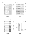
- FIG. 4A shows a sheet of PIC stock, indicated by the general reference character 400 .
- the PIC stock is created by forming a plurality of printed integrated circuits 404 on a first substrate stock 402 , which is depicted as a sheet in this example.
- the printed integrated circuit may contain integrated circuitry, (e.g., CMOS circuitry) fabricated on the substrate using printing and ink technologies as described above.
- the printed integrated circuits can generally be formed with the first substrate stock in any orientation.
- the dashed lines in FIG. 4A denote cross-sheet divisions 406 or down-sheet divisions 408 . If the sheet is formed on a roll, the terms “cross-roll divisions” and “down-roll divisions” can still be employed.
- Cross-sheet (or cross-roll) divisions 406 and down-sheet (or down-roll) divisions 408 denote future divisions of the substrate, whether made during processing or at a future time.
- the sheet or roll may be scored, perforated, or treated by other such similar process to define the division and/or facilitate later division of individual straps.
- FIG. 4B is a view of the PIC stock from the reverse side, or the side opposite the printed integrated circuits.
- the substrate preferably comprising metal foil 422
- the substrate has been removed in selected locations, allowing the remaining metal foil to be used as pads for the printed integrated circuit 424 .
- Backing 426 is applied to the top, or printed integrated circuit side, of the PIC stock.
- Backing 426 may comprise a foil, a film, a sheet, or similar type material, and is typically electrically insulating.
- the film or sheet may be applied per se or as liquid material that is subsequently dried and/or cured to form the film or sheet.
- FIG. 4C An alternative embodiment of the PIC stock, denoted by the general reference character 430 , is depicted in FIG. 4C .
- pads 412 , 414 are formed on each printed integrated circuit 404 and are located on the top side of the PIC stock.
- the sheet may then be cut or otherwise divided into straps or carriers of a size optimized for handling by the attachment machine and matching target parameter values for a particular application.
- the PIC size may be chosen to allow for convenient attachment to ends of an antenna on antenna stock.
- pads 412 , 414 may be separated by a distance about equal to the distance between the ends of the antenna.
- the PIC stock can be divided, either by dividing the PIC stock at all or at selected cross-sheet divisions and/or down-sheet divisions using any process capable of such dividing/separating.
- a roll of PIC stock denoted in FIG. 4D by the general reference character 440 , can be formed from sheets of PIC stock or rolls of PIC stock. Such “n-by-1”/single row or column divisions of the PIC sheet stock can be applied to a backing tape and rolled up into a roll 442 .
- the PIC stock roll can comprise any number of PICs and have a width and/or length corresponding to any unit number of PICs, although a roll one PIC wide is depicted in the figure.
- the roll 442 can comprise printed integrated circuits facing toward or away from the center of the roll. The orientation of the PICs on the roll and the size of the core of the roll may be designed to avoid stress or damage on the PICs.
- Antennas are then formed on a separate substrate using any one of the previously described techniques for forming and/or printing antenna structures.
- the material(s) used for the substrate are selected to be thermally and chemically compatible with RFID and/or EAS tag manufacturing and/or possess appropriate barrier properties.
- the requirements for forming the antenna and subsequent processing i.e. attach process) may enable the use of less expensive substrate materials than used for the printed integrated circuit substrate (thus providing an advantage over an integrated interposer comprising a printed integrated circuit and an antenna and/or inductor.
- the carriers are attached by any of the techniques described previously to the antenna substrate.
- the carriers first may be picked up from the diced substrate sheet and converted into a roll of carriers to facilitate the subsequent attachment process. Since the carrier is size to enable convenient handling by the carrier attach machine, the cost of this process may be optimized to be acceptable low.
- a plurality of rolls of PIC stock are applied to a roll of antenna stock.
- roll of antenna stock 502 comprising a plurality of antennas 507 is unwound in processing equipment.
- the roll may comprise a single antenna or multiple antennas in the cross roll direction.
- the roll has four antennas in the cross-roll direction.
- the roll of PIC stock 504 is unwound, each PIC is placed into contact with each antenna, and the PIC is transferred to the roll of antenna stock 514 .
- Adhesive may be applied to either PIC stock 504 or antenna stock 514 in accordance with techniques known in the art.
- FIG. 6 Another embodiment of the manufacturing method is shown in FIG. 6 .
- This embodiment is a pick-and-place process generally denoted by the general reference character 600 .
- Sheets of antenna substrate 602 are fed toward a robotic placement station where singulated/divided printed integrated circuit carriers, or PICs, 610 are attached to antenna 608 , resulting in a wireless (e.g., RFID) device 610 .
- a robotic machine generally comprising a base and/or control unit 616 , an arm 614 , and a suction or picking device 612 , picks up PIC 610 by maneuvering the arm 614 to the location of PIC 610 , picking up the PIC and placing the PIC onto an antenna 608 .
- Attach steps may be performed prior to PIC placement as desired (e.g., the application of one or more adhesives on the PIC or the antenna). Also, attach steps may be performed after PIC placement as desired (e.g., applying heat and/or pressure to the PIC and antenna to facilitate adhesion, bump-bonding, wire-bonding, ultrasonic bonding, welding, soldering or crimping).
- the workpiece sheet 604 is generally stationary to facilitate an accurate placement operation; however, as lower tolerances are required in this inventive approach, one can appreciate embodiments where sheet 604 may be moving. Once all antennas on sheet 604 have PICs placed on them, sheet 604 advances to the location of completed sheet 606 , and blank sheet 602 advances to the location of workpiece sheet 604 .
- the manufactured devices may be customized at the integrated circuit level (IC) to embed unique identifiers (e.g., a barcode equivalent) and/or response characteristics (e.g., unique time delay in TTF anti-collision schemes using conventional approaches such as those utilizing read-only memory [ROM], one-time programmable [OTP] fuses, and electrically-erasable programmable ROM [EEPROM] elements).
- unique identifiers e.g., a barcode equivalent
- response characteristics e.g., unique time delay in TTF anti-collision schemes using conventional approaches such as those utilizing read-only memory [ROM], one-time programmable [OTP] fuses, and electrically-erasable programmable ROM [EEPROM] elements.
- Alternative approaches to customization utilizing maskless patterning techniques which can be quickly adapted to various applications by changing software parameters can be employed. Examples of maskless patterning techniques include laser patterning and inkjetting, using metal nanoparticle- and/or liquid silane-based inks (see
- inventive manufacturing process enables other manufacturing methods that might otherwise not be possible due to the lower accuracy of placement required when using printed integrated circuits.
- the present invention further relates to method of detecting an item or object in a detection zone comprising the steps of: (i) causing or inducing a current in the present device sufficient for the device to radiate detectable electromagnetic radiation (preferably at a frequency that is an integer multiple or an integer divisor of an applied electromagnetic field), (ii) detecting the detectable electromagnetic radiation, and optionally, (iii) processing information conveyed by the detectable electromagnetic radiation.
- a currents and voltages are induced in the present device sufficient for the device to radiate detectable electromagnetic radiation when the device is in a detection zone comprising an oscillating electromagnetic field. This oscillating electromagnetic field is produced or generated by conventional EAS and/or RFID equipment and/or systems.
- the present method of use may further comprise the step of (iv) transporting or transmitting information from the present device (or sensor) back to a reading device, or (prior to step (i)) attaching or affixing the present device to an object or article (e.g., an identification card, packaging for goods to be shipped, etc.) to be detected, or otherwise including the present device in such an object, article or packaging therefor.
- an object or article e.g., an identification card, packaging for goods to be shipped, etc.
- the present tags are designed at least in part to work with electronic identification and/or security systems that sense disturbances in radio frequency (RF) electromagnetic fields.
- RF radio frequency
- Such electronic systems generally establish an electromagnetic field in a controlled area, defined by portals through which articles must pass in leaving the controlled premises (e.g., a retail store, library, etc.) or a space in which the article must be placed to be read and identified.
- a tag having a resonant circuit is attached to each such article, and the presence of the tag circuit in the controlled area is sensed by a receiving system that detects the tag and processes information obtained therefrom (e.g., determines unauthorized removal of an article or the identity of goods in a container labeled with the tag).
- Most of the tags that operate on these principles are single-use or disposable tags, and are therefore designed to be produced at low cost in very large volumes.
- the present tag may take the form of a sensor, the RF signal modulation characteristics and/or properties of which may change as the characteristics and/or properties of the object or article to which it is attached change.
- the present sensor may be attached to a stainless steel (or other metal) object, structure or surface.
- the properties of the object, structure or surface change e.g., the steel oxidizes, a metal having electromagnetic properties becomes magnetized or carries a minimum threshold electrical current, or the object or surface [regardless of its composition] changes temperature by a predetermined difference or a threshold amount
- the characteristics and/or properties of the RF signal radiated, reflected or modulated by the present sensor also change in a detectable manner.
- the present tags may be used (and, if desired and/or applicable, re-used) in any commercial EAS and/or RFID application and in essentially any frequency range for such applications.
- the present tags may be used at the frequencies, and in the fields and/or ranges, described in Table 1 below:
- the present invention thus also pertains to article surveillance techniques wherein electromagnetic waves are transmitted into an area of the premises being protected at a fundamental frequency (e.g., 13.56 MHz), and the unauthorized presence of articles in the area is sensed by reception and detection of electromagnetic radiation emitted by the present device 100 .
- This emitted electromagnetic radiation may comprise second harmonic or subsequent harmonic frequency waves reradiated from sensor-emitter elements, labels, or films comprising the present device that have been attached to or embedded in the articles, under circumstances in which the labels or films have not been deactivated or otherwise modified for authorized removal from the premises.
- the present invention provides sensor, EAS, RF and/or RFID tags and devices having printed integrated circuitry and an affixed antenna and/or inductor, and methods for their manufacture and use.
- the identification device generally comprises (a) printed integrated circuitry on a first substrate; (b) first and second pads on the first substrate and/or the printed integrated circuitry, electrically coupled to the printed integrated circuitry; and (c) an antenna and/or inductor on a second substrate comprising a conductive line having first and second ends thereon, the first and second ends being in electrical communication with first and second pads, respectively.
- the method of manufacture for a single device generally comprises the steps of (1) printing integrated circuitry having a plurality of first pads on a first substrate; (2) forming an antenna and/or inductor having a plurality of second pads on a second substrate; and (3) attaching at least two of the first pads of the printed integrated circuit to corresponding second pads of the antenna and/or inductor.
- the method of manufacture for multiple devices generally comprises the steps of (A) forming a plurality of printed integrated circuits on a first substrate stock to form a PIC stock; (B) forming a plurality of antennas and/or inductors on a second substrate stock to form an antenna stock; and (C) attaching the PIC stock to the antenna stock.
- the method of use generally comprises the steps of (i) causing or inducing a current in the present device sufficient for the device to radiate, reflect or modulate detectable electromagnetic signals; (ii) detecting the detectable electromagnetic radiation; and optionally, (iii) processing information conveyed by the detectable electromagnetic radiation.
- the method of use may further comprise the step of (iv) transporting or transmitting information from the present device (or sensor) back to a reading device.
- the present invention advantageously provides a low cost RF and/or RFID tag capable of standard applications and operations using conventional RF, RFID and/or EAS equipment and systems.
- a low cost tag may be produced by directly printing or otherwise forming the circuitry on a carrier that is then relatively cheaply attached at relatively low accuracy to an inductor/carrier.
Abstract
Description
| TABLE 1 |
| Exemplary applications. |
| Preferred | ||||
| Range/Field | Range/Field of | |||
| Preferred | of Detection/ | Detection/ | Exemplary Commercial | |
| Frequencies | Frequencies | Response | Response | Application(s) |
| 100-150 KHz | 125-134 KHz | up to 10 feet | up to 5 feet | animal ID, car anti-theft |
| systems, beer keg tracking | ||||
| 5-15 MHz | 8.2 MHz, 9.5 MHz, | up to 10 feet | up to 5 feet | inventory tracking (e.g., |
| 13.56 MHz | libraries, apparel, auto/ | |||
| motorcycle parts), building | ||||
| security/access | ||||
| 800-1000 MHz | 868-928 MHz | up to 30 feet | up to 18 feet | pallet and shipping container |
| tracking, shipyard container | ||||
| tracking | ||||
| 2.4-2.5 GHz | about 2.45 GHz | up to 30 feet | up to 20 feet | auto toll tags |
Claims (36)
Priority Applications (8)
| Application Number | Priority Date | Filing Date | Title |
|---|---|---|---|
| KR1020107007755A KR101539125B1 (en) | 2007-10-10 | 2008-10-10 | Wireless devices including printed integrated circuitry and methods for manufacturing and using the same |
| JP2010529125A JP2011516932A (en) | 2007-10-10 | 2008-10-10 | Wireless device including printed integrated circuit and method of manufacturing and using the same |
| US12/249,707 US9004366B2 (en) | 2007-10-10 | 2008-10-10 | Wireless devices including printed integrated circuitry and methods for manufacturing and using the same |
| CN200880111167.8A CN101896947B (en) | 2007-10-10 | 2008-10-10 | Comprise wireless devices and the making and use method thereof of printed IC |
| CA2702399A CA2702399C (en) | 2007-10-10 | 2008-10-10 | Wireless devices including printed integrated circuitry and methods for manufacturing and using the same |
| PCT/US2008/079653 WO2009049264A1 (en) | 2007-10-10 | 2008-10-10 | Wireless devices including printed integrated circuitry and methods for manufacturing and using the same |
| EP08838217.1A EP2201546B1 (en) | 2007-10-10 | 2008-10-10 | Wireless devices including printed integrated circuitry and methods for manufacturing and using the same |
| JP2014115841A JP5881223B2 (en) | 2007-10-10 | 2014-06-04 | Wireless device including printed integrated circuit and method of manufacturing and using the same |
Applications Claiming Priority (3)
| Application Number | Priority Date | Filing Date | Title |
|---|---|---|---|
| US97905707P | 2007-10-10 | 2007-10-10 | |
| US98058107P | 2007-10-17 | 2007-10-17 | |
| US12/249,707 US9004366B2 (en) | 2007-10-10 | 2008-10-10 | Wireless devices including printed integrated circuitry and methods for manufacturing and using the same |
Publications (2)
| Publication Number | Publication Date |
|---|---|
| US20090095818A1 US20090095818A1 (en) | 2009-04-16 |
| US9004366B2 true US9004366B2 (en) | 2015-04-14 |
Family
ID=40533230
Family Applications (1)
| Application Number | Title | Priority Date | Filing Date |
|---|---|---|---|
| US12/249,707 Expired - Fee Related US9004366B2 (en) | 2007-10-10 | 2008-10-10 | Wireless devices including printed integrated circuitry and methods for manufacturing and using the same |
Country Status (7)
| Country | Link |
|---|---|
| US (1) | US9004366B2 (en) |
| EP (1) | EP2201546B1 (en) |
| JP (2) | JP2011516932A (en) |
| KR (1) | KR101539125B1 (en) |
| CN (1) | CN101896947B (en) |
| CA (1) | CA2702399C (en) |
| WO (1) | WO2009049264A1 (en) |
Cited By (5)
| Publication number | Priority date | Publication date | Assignee | Title |
|---|---|---|---|---|
| US9519904B2 (en) | 2014-10-19 | 2016-12-13 | Thin Film Electronics Asa | NFC/RF mechanism with multiple valid states for detecting an open container, and methods of making and using the same |
| US20180253632A1 (en) * | 2017-03-03 | 2018-09-06 | Thin Film Electronics Asa | Connectable smart label or tag, and methods of making and connecting the same |
| US10860913B2 (en) | 2016-07-15 | 2020-12-08 | Murata Manufacturing Co., Ltd. | RFID tag manufacturing apparatus and method for manufacturing RFID tag |
| US11114321B2 (en) * | 2017-08-17 | 2021-09-07 | Tokyo Electron Limited | Apparatus and method for real-time sensing of properties in industrial manufacturing equipment |
| US11646210B2 (en) | 2018-06-18 | 2023-05-09 | Tokyo Electron Limited | Reduced interference, real-time sensing of properties in manufacturing equipment |
Families Citing this family (27)
| Publication number | Priority date | Publication date | Assignee | Title |
|---|---|---|---|---|
| WO2010127509A1 (en) * | 2009-05-08 | 2010-11-11 | Confidex Ltd. | Rfid transponder |
| US9183973B2 (en) * | 2009-05-28 | 2015-11-10 | Thin Film Electronics Asa | Diffusion barrier coated substrates and methods of making the same |
| GB2491447B (en) * | 2010-03-24 | 2014-10-22 | Murata Manufacturing Co | RFID system |
| KR200461991Y1 (en) * | 2011-12-22 | 2012-08-20 | 주식회사 이그잭스 | a UHF Rfid Tag consisting of a loop sheet and a dipole sheet |
| BR112014019244A8 (en) * | 2012-02-02 | 2017-07-11 | Neo Eco Systems Ltd | SYSTEM AND METHOD FOR THE SALE OF PRODUCTS |
| DE102012010560B4 (en) * | 2012-05-29 | 2020-07-09 | Mühlbauer Gmbh & Co. Kg | Transponder, method for manufacturing a transponder and device for manufacturing the transponder |
| CN203773573U (en) * | 2012-10-12 | 2014-08-13 | 上海中京电子标签集成技术有限公司 | Front body of radio-frequency identification label |
| US9424507B2 (en) * | 2014-04-01 | 2016-08-23 | Nxp B.V. | Dual interface IC card components and method for manufacturing the dual-interface IC card components |
| US9476635B2 (en) * | 2014-06-25 | 2016-10-25 | Haier Us Appliance Solutions, Inc. | Radio frequency identification heat flux measurement systems for refrigerator vacuum insulation panels |
| JP5907365B1 (en) * | 2014-11-07 | 2016-04-26 | 株式会社村田製作所 | RADIO COMMUNICATION DEVICE AND MANUFACTURING METHOD THEREOF, SEAL WITH RFIC ELEMENT AND MANUFACTURING METHOD THEREOF |
| EP3091483B1 (en) | 2014-11-07 | 2020-08-12 | Murata Manufacturing Co., Ltd. | Wireless communication device, method for manufacturing same, and method for producing seal fitted with rfic element |
| CN107533658A (en) * | 2015-04-10 | 2018-01-02 | 薄膜电子有限公司 | The sensor-based more effective status NFC/RF mechanisms for opening or being damaged for detection container |
| WO2016203882A1 (en) * | 2015-06-18 | 2016-12-22 | 株式会社村田製作所 | Carrier tape, method for manufacturing same, and method for manufacturing rfid tag |
| US20180285706A1 (en) * | 2015-10-06 | 2018-10-04 | Thin Film Electronics Asa | Electronic Device Having an Antenna, Metal Trace(s) and/or Inductor With a Printed Adhesion Promoter Thereon, and Methods of Making and Using the Same |
| KR20180071283A (en) | 2015-10-21 | 2018-06-27 | 도레이 카부시키가이샤 | Capacitor, method of manufacturing the same, and wireless communication device using the same |
| EP3387673A4 (en) * | 2015-12-11 | 2019-07-24 | Thin Film Electronics ASA | Electronic device having a plated antenna and/or trace, and methods of making and using the same |
| CN109415146A (en) * | 2016-04-18 | 2019-03-01 | 薄膜电子有限公司 | The manufacture and application method of bottle with intelligent label and the intelligent label for bottle |
| CN105868823A (en) * | 2016-06-03 | 2016-08-17 | 广东楚天龙智能卡有限公司 | Coil for dual-interface IC card with high production yield, IC card adopting coil and production method of IC card |
| US20180158788A1 (en) * | 2016-12-01 | 2018-06-07 | Avery Dennison Retail Information Services, Llc | Mixed structure method of layout of different size elements to optimize the area usage on a wafer |
| CN107219028A (en) * | 2017-05-05 | 2017-09-29 | 华东师范大学 | A kind of preparation method of the flexible wireless pressure detecting system based on inkjet technology |
| SE542007C2 (en) * | 2017-10-13 | 2020-02-11 | Stora Enso Oyj | A method and an apparatus for producing a radio-frequency identification transponder |
| US10783418B2 (en) * | 2017-10-16 | 2020-09-22 | Semtech Corporation | Transmitting tag |
| CN110600439A (en) * | 2018-06-12 | 2019-12-20 | 深圳市环基实业有限公司 | RFID chip and manufacturing method thereof |
| WO2020086532A1 (en) | 2018-10-22 | 2020-04-30 | Thin Film Electronics Asa | Barrier stacks for printed and/or thin film electronics methods of manufacturing the same, and method of controlling a threshold voltage of a thin film transistor |
| JP2022537392A (en) * | 2019-06-20 | 2022-08-25 | テトラ ラバル ホールディングス アンド ファイナンス エス エイ | Method for packaging material |
| US11281874B2 (en) * | 2020-06-11 | 2022-03-22 | The Board Of Trustees Of The Leland Stanford Junior University | Flexible tag device and flexible sensing system comprising the same |
| DE102020209307A1 (en) * | 2020-07-23 | 2022-01-27 | Robert Bosch Gesellschaft mit beschränkter Haftung | Radar sensor with waveguide structure |
Citations (20)
| Publication number | Priority date | Publication date | Assignee | Title |
|---|---|---|---|---|
| US5528222A (en) | 1994-09-09 | 1996-06-18 | International Business Machines Corporation | Radio frequency circuit and memory in thin flexible package |
| US6100804A (en) | 1998-10-29 | 2000-08-08 | Intecmec Ip Corp. | Radio frequency identification system |
| US6509217B1 (en) | 1999-10-22 | 2003-01-21 | Damoder Reddy | Inexpensive, reliable, planar RFID tag structure and method for making same |
| US6693541B2 (en) | 2001-07-19 | 2004-02-17 | 3M Innovative Properties Co | RFID tag with bridge circuit assembly and methods of use |
| US6891110B1 (en) | 1999-03-24 | 2005-05-10 | Motorola, Inc. | Circuit chip connector and method of connecting a circuit chip |
| US20050130389A1 (en) * | 2003-12-12 | 2005-06-16 | Semiconductor Energy Laboratory Co., Ltd. | Semiconductor device and manufacturing method thereof |
| US20050134463A1 (en) | 2003-12-19 | 2005-06-23 | Semiconductor Energy Laboratory Co., Ltd. | Semiconductor device, RFID tag and label-like object |
| US20050136358A1 (en) * | 2003-12-19 | 2005-06-23 | Palo Alto Research Center Incorporated | Patterning using wax printing and lift off |
| JP2005228298A (en) | 2003-12-19 | 2005-08-25 | Semiconductor Energy Lab Co Ltd | Semiconductor apparatus and method for manufacturing the same |
| US20050198811A1 (en) | 2004-03-12 | 2005-09-15 | A K Stamping Co. Inc. | Manufacture of RFID tags and intermediate products therefor |
| US6951596B2 (en) | 2002-01-18 | 2005-10-04 | Avery Dennison Corporation | RFID label technique |
| US20060145710A1 (en) * | 2004-12-22 | 2006-07-06 | Puleston David J | Method and system for testing RFID devices |
| US20060226238A1 (en) * | 2003-07-15 | 2006-10-12 | Axalto S.A. | Chip card including tamper-proof security features |
| US20060254440A1 (en) * | 2005-04-13 | 2006-11-16 | Korea Institute Of Machinery & Materials | Method and apparatus for manufacturing electronic device using roll-to-roll rotary pressing process |
| US20060270191A1 (en) * | 2005-05-31 | 2006-11-30 | Semiconductor Energy Laboratory Co., Ltd. | Manufacturing method of semiconductor device |
| US20070090955A1 (en) | 2005-10-25 | 2007-04-26 | Checkpoint Systems, Inc. | Capacitor strap |
| US7292148B2 (en) | 2004-06-18 | 2007-11-06 | Avery Dennison Corporation | Method of variable position strap mounting for RFID transponder |
| US7307527B2 (en) | 2004-07-01 | 2007-12-11 | Avery Dennison Corporation | RFID device preparation system and method |
| US7359823B2 (en) | 2005-05-25 | 2008-04-15 | Avery Dennison | RFID device variable test systems and methods |
| US7413124B2 (en) | 2005-07-19 | 2008-08-19 | 3M Innovative Properties Company | RFID reader supporting one-touch search functionality |
Family Cites Families (2)
| Publication number | Priority date | Publication date | Assignee | Title |
|---|---|---|---|---|
| EP1039543B1 (en) * | 1999-03-24 | 2014-02-26 | Motorola Solutions, Inc. | Circuit chip connector and method of connecting a circuit chip |
| JP4761779B2 (en) * | 2004-01-23 | 2011-08-31 | 株式会社半導体エネルギー研究所 | ID labels, ID cards, ID tags, and articles |
-
2008
- 2008-10-10 WO PCT/US2008/079653 patent/WO2009049264A1/en active Application Filing
- 2008-10-10 US US12/249,707 patent/US9004366B2/en not_active Expired - Fee Related
- 2008-10-10 CN CN200880111167.8A patent/CN101896947B/en not_active Expired - Fee Related
- 2008-10-10 KR KR1020107007755A patent/KR101539125B1/en active IP Right Grant
- 2008-10-10 CA CA2702399A patent/CA2702399C/en not_active Expired - Fee Related
- 2008-10-10 JP JP2010529125A patent/JP2011516932A/en active Pending
- 2008-10-10 EP EP08838217.1A patent/EP2201546B1/en not_active Not-in-force
-
2014
- 2014-06-04 JP JP2014115841A patent/JP5881223B2/en not_active Expired - Fee Related
Patent Citations (21)
| Publication number | Priority date | Publication date | Assignee | Title |
|---|---|---|---|---|
| US5528222A (en) | 1994-09-09 | 1996-06-18 | International Business Machines Corporation | Radio frequency circuit and memory in thin flexible package |
| US6100804A (en) | 1998-10-29 | 2000-08-08 | Intecmec Ip Corp. | Radio frequency identification system |
| US6891110B1 (en) | 1999-03-24 | 2005-05-10 | Motorola, Inc. | Circuit chip connector and method of connecting a circuit chip |
| US6509217B1 (en) | 1999-10-22 | 2003-01-21 | Damoder Reddy | Inexpensive, reliable, planar RFID tag structure and method for making same |
| US6693541B2 (en) | 2001-07-19 | 2004-02-17 | 3M Innovative Properties Co | RFID tag with bridge circuit assembly and methods of use |
| US6951596B2 (en) | 2002-01-18 | 2005-10-04 | Avery Dennison Corporation | RFID label technique |
| US20060226238A1 (en) * | 2003-07-15 | 2006-10-12 | Axalto S.A. | Chip card including tamper-proof security features |
| US20050130389A1 (en) * | 2003-12-12 | 2005-06-16 | Semiconductor Energy Laboratory Co., Ltd. | Semiconductor device and manufacturing method thereof |
| US20050136358A1 (en) * | 2003-12-19 | 2005-06-23 | Palo Alto Research Center Incorporated | Patterning using wax printing and lift off |
| JP2005228298A (en) | 2003-12-19 | 2005-08-25 | Semiconductor Energy Lab Co Ltd | Semiconductor apparatus and method for manufacturing the same |
| US20050134463A1 (en) | 2003-12-19 | 2005-06-23 | Semiconductor Energy Laboratory Co., Ltd. | Semiconductor device, RFID tag and label-like object |
| US20050198811A1 (en) | 2004-03-12 | 2005-09-15 | A K Stamping Co. Inc. | Manufacture of RFID tags and intermediate products therefor |
| US7292148B2 (en) | 2004-06-18 | 2007-11-06 | Avery Dennison Corporation | Method of variable position strap mounting for RFID transponder |
| US7307527B2 (en) | 2004-07-01 | 2007-12-11 | Avery Dennison Corporation | RFID device preparation system and method |
| US20060145710A1 (en) * | 2004-12-22 | 2006-07-06 | Puleston David J | Method and system for testing RFID devices |
| US20060254440A1 (en) * | 2005-04-13 | 2006-11-16 | Korea Institute Of Machinery & Materials | Method and apparatus for manufacturing electronic device using roll-to-roll rotary pressing process |
| US7359823B2 (en) | 2005-05-25 | 2008-04-15 | Avery Dennison | RFID device variable test systems and methods |
| US20060270191A1 (en) * | 2005-05-31 | 2006-11-30 | Semiconductor Energy Laboratory Co., Ltd. | Manufacturing method of semiconductor device |
| US7413124B2 (en) | 2005-07-19 | 2008-08-19 | 3M Innovative Properties Company | RFID reader supporting one-touch search functionality |
| US20070090955A1 (en) | 2005-10-25 | 2007-04-26 | Checkpoint Systems, Inc. | Capacitor strap |
| EP1952316B1 (en) | 2005-10-25 | 2011-12-21 | Checkpoint Systems, Inc. | Capacitor strap |
Non-Patent Citations (7)
| Title |
|---|
| Chinese Office Action with English translation dated Feb. 13, 2012; Chinese Patent Application No. 200880111167.8; 7 pages total; The State Intellectual Property Office of the P.R.C., People's Republic of China. |
| International Preliminary Report on Patentability, International Pat. Appl. No. PCT/US2008/079653, mailed from the IPEA/US on Mar. 22, 2013. |
| Maekawa et al., "Semiconductor Apparatus and Method for Manufacturing the Same", Patent Abstracts of Japan, Japanese Patent Publication No. 2005-228298, Aug. 25, 2005, http://www.19.ipdl.inpit.go.jp/PA1?result/detail/main/wn4idaaDA417228298P1.htm. |
| Office Action from Korean Intellectual Property Office with partial English translation in Korean Patent Application No. 10-2010-7007755 dated Jan. 29, 2015; 13 pgs. |
| Office Action, Japanese Pat. Appl. No. 2010-529125, mailed from the Japan Patent Office on Feb. 20, 2013. |
| Patrick Smith, Criswell Choi, Vikram Pavate, James Montgue Cleeves, Vivek Subramanian, Vince Biviano and Richard Young; "Wireless Devices Including Printed Integrated Circuitry and Methods for Manufacturing and Using the Same"; International Search Report, PCT Application No. PCT/US 08/79653; 2 pages; International Searching Authority/United States, Commissioner for Patents, Alexandria, Virginia, Dec. 18, 2008. |
| Patrick Smith, Criswell Choi, Vikram Pavate, James Montgue Cleeves, Vivek Subramanian, Vince Biviano and Richard Young; "Wireless Devices Including Printed Integrated Circuitry and Methods for Manufacturing and Using the Same"; Written Opinion, PCT Application No. PCT/US 08/79653; 5 pages; International Searching Authority/United States, Commissioner for Patents, Alexandria, Virginia, Dec. 18, 2008. |
Cited By (10)
| Publication number | Priority date | Publication date | Assignee | Title |
|---|---|---|---|---|
| US9519904B2 (en) | 2014-10-19 | 2016-12-13 | Thin Film Electronics Asa | NFC/RF mechanism with multiple valid states for detecting an open container, and methods of making and using the same |
| US9846835B2 (en) | 2014-10-19 | 2017-12-19 | Thin Film Electronics, Asa | NFC/RF mechanism with multiple valid states for detecting an open container, and methods of making and using the same |
| US10115053B2 (en) | 2014-10-19 | 2018-10-30 | Thin Film Electronics Asa | NFC/RF mechanism with multiple valid states for detecting an open container, and methods of making and using the same |
| US10360493B2 (en) | 2014-10-19 | 2019-07-23 | Thin Film Electronics Asa | NFC/RF mechanism with multiple valid states for detecting an open container, and methods of making and using the same |
| US10579919B2 (en) | 2014-10-19 | 2020-03-03 | Thin Film Electronics Asa | NFC/RF mechanism with multiple valid states for detecting an open container, and methods of making and using the same |
| US10860913B2 (en) | 2016-07-15 | 2020-12-08 | Murata Manufacturing Co., Ltd. | RFID tag manufacturing apparatus and method for manufacturing RFID tag |
| US20180253632A1 (en) * | 2017-03-03 | 2018-09-06 | Thin Film Electronics Asa | Connectable smart label or tag, and methods of making and connecting the same |
| WO2018160755A1 (en) * | 2017-03-03 | 2018-09-07 | Thin Film Electronics Asa | Connectable smart label or tag, and methods of making and connecting the same |
| US11114321B2 (en) * | 2017-08-17 | 2021-09-07 | Tokyo Electron Limited | Apparatus and method for real-time sensing of properties in industrial manufacturing equipment |
| US11646210B2 (en) | 2018-06-18 | 2023-05-09 | Tokyo Electron Limited | Reduced interference, real-time sensing of properties in manufacturing equipment |
Also Published As
| Publication number | Publication date |
|---|---|
| JP2014160515A (en) | 2014-09-04 |
| CN101896947A (en) | 2010-11-24 |
| EP2201546A4 (en) | 2016-06-22 |
| JP2011516932A (en) | 2011-05-26 |
| CA2702399A1 (en) | 2009-04-16 |
| US20090095818A1 (en) | 2009-04-16 |
| EP2201546B1 (en) | 2018-10-03 |
| EP2201546A1 (en) | 2010-06-30 |
| CA2702399C (en) | 2019-01-08 |
| KR20100065186A (en) | 2010-06-15 |
| KR101539125B1 (en) | 2015-07-23 |
| CN101896947B (en) | 2016-05-11 |
| WO2009049264A1 (en) | 2009-04-16 |
| JP5881223B2 (en) | 2016-03-09 |
Similar Documents
| Publication | Publication Date | Title |
|---|---|---|
| US9004366B2 (en) | Wireless devices including printed integrated circuitry and methods for manufacturing and using the same | |
| US9361573B2 (en) | Printed antennas, methods of printing an antenna, and devices including the printed antenna | |
| US9953259B2 (en) | RF and/or RF identification tag/device having an integrated interposer, and methods for making and using the same | |
| US7967204B2 (en) | Assembly comprising a functional device and a resonator and method of making same | |
| JP4233554B2 (en) | Combination of identification element and safety element and manufacturing method thereof | |
| US9171245B2 (en) | Chip arrangement, analysis apparatus, receiving container, and receiving container system | |
| CN101377826B (en) | Radio frequency and/or radio frequency identification electronic filemark/ apparatus with integration substrate, and manufacturing and using method thereof | |
| EP2026254B1 (en) | RF and/or RF identification tag/device having an integrated interposer, and methods for making and using the same | |
| TWI384401B (en) | Rf and/or rf identification tag/device having an integrated interposer, and methods for making and using the same | |
| CA2606999C (en) | Rf and/or rf identification tag/device having an integrated interposer, and methods for making the same | |
| JP5473017B2 (en) | RF tag / device and / or RFID tag / device having an integrated interposer, and methods for making and using the same | |
| KR100962570B1 (en) | RF and/or RF Identification Tag/Device Having An Integrated Interposer, And Methods For Making And Using The Same | |
| KR20090084499A (en) | Method for manufacturing radio frequency identification tag and radio frequency identification tag manufactured by the method |
Legal Events
| Date | Code | Title | Description |
|---|---|---|---|
| AS | Assignment |
Owner name: KOVIO, INC., CALIFORNIA Free format text: ASSIGNMENT OF ASSIGNORS INTEREST;ASSIGNOR:BIVIANO, VINCE;REEL/FRAME:021899/0579 Effective date: 20081010 Owner name: KOVIO, INC., CALIFORNIA Free format text: ASSIGNMENT OF ASSIGNORS INTEREST;ASSIGNORS:SMITH, PATRICK;CHOI, CRISWELL;PAVATE, VIKRAM;AND OTHERS;REEL/FRAME:021899/0506;SIGNING DATES FROM 20081009 TO 20081030 Owner name: KOVIO, INC., CALIFORNIA Free format text: ASSIGNMENT OF ASSIGNORS INTEREST;ASSIGNOR:CLEEVES, JAMES MONTAGUE;REEL/FRAME:021899/0582 Effective date: 20081009 Owner name: KOVIO, INC., CALIFORNIA Free format text: ASSIGNMENT OF ASSIGNORS INTEREST;ASSIGNORS:SMITH, PATRICK;CHOI, CRISWELL;PAVATE, VIKRAM;AND OTHERS;SIGNING DATES FROM 20081009 TO 20081030;REEL/FRAME:021899/0506 |
|
| AS | Assignment |
Owner name: THIN FILM ELECTRONICS ASA, NORWAY Free format text: ASSIGNMENT OF ASSIGNORS INTEREST;ASSIGNOR:KOVIO, INC.;REEL/FRAME:032126/0931 Effective date: 20140122 |
|
| STCF | Information on status: patent grant |
Free format text: PATENTED CASE |
|
| MAFP | Maintenance fee payment |
Free format text: PAYMENT OF MAINTENANCE FEE, 4TH YR, SMALL ENTITY (ORIGINAL EVENT CODE: M2551); ENTITY STATUS OF PATENT OWNER: SMALL ENTITY Year of fee payment: 4 |
|
| AS | Assignment |
Owner name: UTICA LEASECO, LLC, MICHIGAN Free format text: SECURITY INTEREST;ASSIGNORS:THIN FILM ELECTRONICS, INC.;THIN FILM ELECTRONICS, ASA;REEL/FRAME:053472/0129 Effective date: 20200604 |
|
| AS | Assignment |
Owner name: ENSURGE MICROPOWER ASA, CALIFORNIA Free format text: CHANGE OF NAME;ASSIGNOR:THIN FILM ELECTRONICS ASA;REEL/FRAME:061298/0249 Effective date: 20220819 |
|
| FEPP | Fee payment procedure |
Free format text: MAINTENANCE FEE REMINDER MAILED (ORIGINAL EVENT CODE: REM.); ENTITY STATUS OF PATENT OWNER: SMALL ENTITY |
|
| LAPS | Lapse for failure to pay maintenance fees |
Free format text: PATENT EXPIRED FOR FAILURE TO PAY MAINTENANCE FEES (ORIGINAL EVENT CODE: EXP.); ENTITY STATUS OF PATENT OWNER: SMALL ENTITY |
|
| STCH | Information on status: patent discontinuation |
Free format text: PATENT EXPIRED DUE TO NONPAYMENT OF MAINTENANCE FEES UNDER 37 CFR 1.362 |
|
| FP | Lapsed due to failure to pay maintenance fee |
Effective date: 20230414 |