US8995173B1 - Memory cells, devices and method with dynamic storage elements and programmable impedance shadow elements - Google Patents
Memory cells, devices and method with dynamic storage elements and programmable impedance shadow elements Download PDFInfo
- Publication number
- US8995173B1 US8995173B1 US13/603,373 US201213603373A US8995173B1 US 8995173 B1 US8995173 B1 US 8995173B1 US 201213603373 A US201213603373 A US 201213603373A US 8995173 B1 US8995173 B1 US 8995173B1
- Authority
- US
- United States
- Prior art keywords
- dynamic
- memory cells
- programmable impedance
- elements
- memory
- Prior art date
- Legal status (The legal status is an assumption and is not a legal conclusion. Google has not performed a legal analysis and makes no representation as to the accuracy of the status listed.)
- Active, expires
Links
Images


Classifications
-
- G—PHYSICS
- G11—INFORMATION STORAGE
- G11C—STATIC STORES
- G11C11/00—Digital stores characterised by the use of particular electric or magnetic storage elements; Storage elements therefor
- G11C11/21—Digital stores characterised by the use of particular electric or magnetic storage elements; Storage elements therefor using electric elements
- G11C11/34—Digital stores characterised by the use of particular electric or magnetic storage elements; Storage elements therefor using electric elements using semiconductor devices
- G11C11/40—Digital stores characterised by the use of particular electric or magnetic storage elements; Storage elements therefor using electric elements using semiconductor devices using transistors
- G11C11/401—Digital stores characterised by the use of particular electric or magnetic storage elements; Storage elements therefor using electric elements using semiconductor devices using transistors forming cells needing refreshing or charge regeneration, i.e. dynamic cells
-
- G—PHYSICS
- G11—INFORMATION STORAGE
- G11C—STATIC STORES
- G11C13/00—Digital stores characterised by the use of storage elements not covered by groups G11C11/00, G11C23/00, or G11C25/00
- G11C13/0002—Digital stores characterised by the use of storage elements not covered by groups G11C11/00, G11C23/00, or G11C25/00 using resistive RAM [RRAM] elements
- G11C13/0007—Digital stores characterised by the use of storage elements not covered by groups G11C11/00, G11C23/00, or G11C25/00 using resistive RAM [RRAM] elements comprising metal oxide memory material, e.g. perovskites
-
- G—PHYSICS
- G11—INFORMATION STORAGE
- G11C—STATIC STORES
- G11C13/00—Digital stores characterised by the use of storage elements not covered by groups G11C11/00, G11C23/00, or G11C25/00
- G11C13/0002—Digital stores characterised by the use of storage elements not covered by groups G11C11/00, G11C23/00, or G11C25/00 using resistive RAM [RRAM] elements
- G11C13/0009—RRAM elements whose operation depends upon chemical change
- G11C13/0011—RRAM elements whose operation depends upon chemical change comprising conductive bridging RAM [CBRAM] or programming metallization cells [PMCs]
-
- G—PHYSICS
- G11—INFORMATION STORAGE
- G11C—STATIC STORES
- G11C14/00—Digital stores characterised by arrangements of cells having volatile and non-volatile storage properties for back-up when the power is down
- G11C14/0009—Digital stores characterised by arrangements of cells having volatile and non-volatile storage properties for back-up when the power is down in which the volatile element is a DRAM cell
- G11C14/0045—Digital stores characterised by arrangements of cells having volatile and non-volatile storage properties for back-up when the power is down in which the volatile element is a DRAM cell and the nonvolatile element is a resistive RAM element, i.e. programmable resistors, e.g. formed of phase change or chalcogenide material
Definitions
- the present disclosure relates generally to memory devices, and more particularly to memory devices with memory cells that include both dynamic storage elements and programmable impedance elements.
- DRAMs Dynamic random access memories
- DRAM memory cells can have the disadvantages of being volatile (i.e., losing a stored data value in the absence of power) and of requiring refresh (i.e., data values must be re-written periodically to avoid losing data).
- DRAMs can operate at relatively low power consumption levels, and can provide relatively fast data access speeds for read and write operations.
- a storage capability separate from the DRAM device such as a nonvolatile storage integrated circuit (chip) or other nonvolatile storage, such as a hard disk drive.
- FIG. 1 is a schematic diagram of a memory cell according to one embodiment.
- FIGS. 2A to 2D are a schematic showing operations of a memory cell like that of FIG. 1 .
- FIG. 3 is a schematic diagram of a memory cell according to another embodiment having a capacitor as a dynamic storage element and a programmable impedance element directly connected to a storage node.
- FIG. 4 is a schematic diagram of a memory cell according to a further embodiment having a capacitor as a dynamic storage element and a programmable impedance element connected to a storage node by an access device.
- FIG. 5 is a schematic diagram of a memory cell according to another embodiment having a capacitor as a dynamic storage element and a programmable metallization cell (PMC) as a programmable storage element.
- PMC programmable metallization cell
- FIG. 6 is a block schematic diagram of a memory device according to an embodiment.
- FIG. 7 is a block schematic diagram of a memory device according to a further embodiment.
- FIG. 8 is a block schematic diagram of a memory device according to another embodiment.
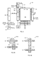
- FIGS. 9A to 9D are to plan views of memory cells according to various embodiments.
- FIGS. 10A to 10C are side cross sectional views showing memory cells with access devices formed in a same substrate according to various embodiments.
- FIGS. 11A and 11B are side cross sectional views showing memory cells with an access device formed above a substrate according to embodiments.
- FIG. 12 is a flow diagram of a method according to one embodiment.
- FIG. 13 is a flow diagram of a method according to another embodiment.
- Embodiments disclosed herein show memory cells, devices and methods having both dynamic storage elements and programmable impedance elements.
- dynamic storage elements can be accessed for read and write operations at high speeds.
- Programmable impedance elements can “shadow” the dynamic storage elements by storing the same data values as the dynamic storage elements.
- data values stored in the dynamic elements can be stored in the programmable impedance elements. In some embodiments, this can enable data to be stored in a nonvolatile or quasi-nonvolatile fashion. Further, when it is once again desirable to use the dynamic storage elements, data values can be loaded from the programmable impedance elements back into the dynamic storage elements.
- FIG. 1 is a block schematic diagram of a memory cell 100 according to a first embodiment.
- a memory cell 100 can include a dynamic section 102 and a programmable impedance section 104 .
- memory cell 100 can be connected to a word line 106 and a bit line 108 . It is understood that a memory cell 100 can be repeated numerous times in an array, with memory cells of a same column being connected to a same bit line 108 , and memory cells of a same row being connected to a same word line 106 .
- a dynamic section 102 can store a data value in a dynamic fashion, losing a stored data value in the absence of applied power.
- a dynamic section 102 can be connected to bit line 108 and word line 106 . In such an arrangement, a data value can be read from and written into a dynamic section 102 .
- a programmable impedance section 104 can include one or more programmable impedance elements that can be programmed into two or more impedance states.
- a programmable impedance section 104 can connect its programmable impedance element 104 to the dynamic section 102 in response to an access signal PZ_Acc.
- FIGS. 2A to 2D show various operations of memory cell 100 according to embodiments.
- FIG. 2A shows a WRITE operation to memory cell 100 according to one embodiment.
- a word line 106 can be driven to an active level, connecting dynamic section 102 to bit line 108 .
- Bit line 108 can be driven to a potential according to a write data value. In FIG. 2A , this is represented by a “1” value.
- a data value stored by dynamic section 102 can be set to store one value (shown as ? ⁇ 1).
- PZ_Acc in a WRITE operation, PZ_Acc can be driven to an inactive level, isolating programmable impedance section 104 from dynamic section 102 .
- a WRITE operation can be conceptualized as a “standard” operation, as it accesses the dynamic section 102 and not the programmable impedance section 104 . As such, a WRITE operation can have a same or similar performance of a conventional dynamic memory device.
- FIG. 2B shows a LOAD operation for memory cell 100 according to one embodiment.
- a word line 106 can be driven to an inactive level, isolating dynamic section 102 from bit line 108 .
- PZ_Acc can be driven to an active level, connecting programmable impedance section 104 to dynamic section 102 .
- programmable impedance element(s) within programmable impedance section 104 can be programmed to store the data value stored by the dynamic section (shown as ? ⁇ 1).
- a LOAD operation can be considered a non-standard operation, as it stores data in programmable impedance elements. Such an action can store data in a nonvolatile or quasi-nonvolatile fashion.
- a data value can be stored in programmable impedance section 104 in the absence of power.
- programmable impedance section 104 can store a data value for longer periods of time than a dynamic section 102 . In some embodiments, such storage times can be orders of magnitude longer than a dynamic section 102 . For example, if a dynamic section refreshes data at a rate of every tens or hundreds of microseconds, a programmable impedance section can retain data values on the order of milliseconds, seconds, minutes, or hours.
- FIG. 2C shows a RECALL operation for memory cell 100 according to one embodiment.
- a word line 106 can be driven to an inactive level, isolating dynamic section 102 from bit line 108 .
- PZ_Acc can be driven to an active level, connecting programmable impedance section 104 to dynamic section 102 .
- programmable impedance element(s) within programmable impedance section 104 can establish the data value stored in dynamic section (shown as ? ⁇ 1).
- a RECALL operation can be considered a non-standard operation, as it accesses programmable impedance elements.
- FIG. 2D shows a READ operation from memory cell 100 according to one embodiment.
- a word line 106 can be driven to an active level, connecting dynamic section 102 to bit line 108 .
- a bit line 108 can be driven to a potential (or can draw a particular current). This is represented by the “1” being placed on bit line 108 .
- PZ_Acc in a READ operation, PZ_Acc can be driven to an inactive level, isolating programmable impedance section 104 from dynamic section 102 .
- a READ operation can be conceptualized as a “standard” operation, as it accesses the dynamic section 102 and not the programmable impedance section 104 . As such, like the WRITE operation, a READ operation can have a same or similar performance of a conventional dynamic memory device.
- FIG. 3 is a schematic diagram of a memory cell 300 according to another embodiment.
- memory cell 300 can be one implementation of that shown in FIG. 1 .
- a memory cell 300 can include a dynamic section 302 and programmable impedance section 304 .
- a dynamic section 302 can be a dynamic RAM section formed by a first access device 316 and a storage capacitor C1.
- a first access device 316 can be connected between a bit line 308 and capacitor C1, and can have a control terminal connected to a first word line 306 .
- Capacitor C1 can have one terminal connected to a storage node 320 and another terminal connected to a first common node 312 .
- Capacitor C1 can store (or not store) charge to indicate a data value in a dynamic fashion.
- first common node 312 can be a capacitor plate common to multiple storage capacitors.
- Capacitor C1 can have a bit-line-over-contact (BOC) configuration, a capacitor-over-bit line (COB) configuration, or can be a trench type capacitor, including a trench capacitor with a substrate plate, or a trench capacitor with a substrate storage node.
- BOC bit-line-over-contact
- COB capacitor-over-bit line
- a programmable impedance section 304 can include a second access device 318 and a programmable impedance element 322 .
- a second access device 318 can be connected between programmable impedance element 322 and second common node 314 , and can have a control terminal connected to a second word line 310 .
- a programmable impedance element 322 can be a two terminal element having one terminal connected to storage node 320 and another terminal connected to second access device 318 .
- a programmable impedance element 322 can be programmed between two or more impedance states by application of an electric field. In one embodiment, element 322 can be programmed between at least two different resistance states. In some embodiments, an element 322 can include a solid ion conductor layer formed between two electrodes. In very particular embodiments, an element 322 can be a programmable metallization cell (PMC) (also referred to as a conductive bridging random access memory (CBRAM) type cell). In some PMC embodiments, an element 322 can include an active electrode (anode) and an indifferent electrode (cathode) with a solid ion conductor layer formed between. An active electrode can be a source of conductive ions that can establish the impedance state of the PMC.
- PMC programmable metallization cell
- CBRAM conductive bridging random access memory
- Either of the access devices 316 / 318 can be an active circuit element, including any suitable transistor.
- access devices 316 / 318 can be insulated gate field effect (e.g., MOS) type transistors.
- Either access device 316 / 318 can be formed in a semiconductor substrate.
- either of access devices 316 / 318 can be a thin-film transistor formed over a substrate.
- a memory cell 300 can be conceptualized as having two modes of operation.
- a memory cell 300 can operate in a standard DRAM like fashion, accessing dynamic section 302 , while programmable impedance section 304 remains isolated from dynamic section 302 .
- first access device 316 can be enabled according to a signal on first word line 306 , connecting bit line 308 to storage node 320 .
- second access device 318 can be disabled according to a signal on second word line 310 , isolating element 322 from common node 314 .
- data can be written into the dynamic section 302 by driving bit line 308 to a predetermined potential, while maintaining first common node 312 at one potential.
- capacitor C1 can be charged or not charge via bit line 308 to store a data value.
- data can be read from dynamic section 302 by enabling first access device 316 to allow charge (or lack of charge) to be shared with bit line 308 , depending upon a charged state of capacitor C1.
- a memory cell 300 can enable data held in the dynamic section 302 to be stored in programmable impedance section 304 , or loaded from programmable impedance section 304 into the dynamic section 302 .
- first access device 316 can be disabled according to a signal on first word line 306 , isolating bit line 308 from storage node 320 .
- second access device 318 can be enabled according to a signal on second word line 310 , connecting element 322 to common node 314 .
- a programmable impedance element 322 can be programmed by driving second common node 314 to a predetermined potential, while a charge state of capacitor C1 establishes a potential on storage node 320 . If a sufficient voltage is created across element 322 , the element 322 can be programmed to an impedance state. Similarly, a capacitor C1 can be charged according to a state of element 322 by driving common nodes 312 and 314 to different potentials. In such an arrangement, capacitor C1 can be charged or not charged according to a programmed resistance of element 322 .
- FIG. 4 is a schematic diagram of a memory cell 400 according to another embodiment.
- FIG. 4 includes items like those of FIG. 3 , and such like items are referred to by the same reference character but with the first digit being “4”.
- FIG. 4 differs from FIG. 3 in that a second access device 418 can be connected between storage node 420 and programmable impedance element 422 .
- the memory cell 400 of FIG. 4 can operate in the same general fashion as described for FIG. 3 .
- FIG. 5 is a schematic diagram of a memory cell 500 according to another embodiment.
- FIG. 5 includes items like those of FIG. 3 , and such like items are referred to by the same reference character but with the first digit being “5”.
- FIG. 5 differs from FIG. 3 in that access devices 516 / 518 are shown as n-channel insulated gate field effect (MOS type) transistors, and programmable impedance element 522 can be a PMC type element, having a solid ion conductor formed between two electrodes.
- PMC element 522 can have an anode connected to storage node 520 and a cathode connected to second access device 518 .
- MOS type insulated gate field effect
- FIG. 5 shows a memory cell like that of FIG. 3
- alternate embodiments can include a configuration like that of FIG. 4 .
- either of access devices can be p-channel MOS type transistors.
- the anode-cathode connection can be switched (i.e., a cathode can be connected to a storage node and an anode can be connected to a second common node).
- FIG. 6 is a block schematic diagram showing a memory device 630 according to one embodiment.
- a memory device 630 can include memory cells 600 - 0 / 1 arranged into at least one row 624 .
- Memory cells 600 - 0 / 1 of a same row can be commonly connected to same first and second word lines 606 / 610 and first and second common nodes 612 / 614 .
- Memory cells 600 - 0 / 1 can each be connected to different bit lines 608 - 0 / 1 .
- Memory cells 600 - 0 / 1 can take the form of any of those shown herein, or equivalents, including a dynamic section 602 and a programmable impedance section 604 .
- Any of the READ, WRITE, LOAD, and RECALL operations can be performed on memory cells ( 600 - 0 / 1 ) in parallel. That is, data can be read from memory cells ( 600 - 0 / 1 ) on bit lines ( 608 - 0 / 1 ) simultaneously. Data can be written into memory cells ( 600 - 0 / 1 ) from bit lines ( 608 - 0 / 1 ) simultaneously. Further, data can be stored into programmable impedance sections 604 from dynamic sections 602 in parallel, and recalled from programmable impedance sections 604 into dynamic sections 602 in parallel.
- a memory device can be a DRAM with PMC type cells operating as “shadow” cells to the DRAM cells.
- a PMC type shadow cell can store a data value for a longer period of time than a DRAM cell, and in some embodiments, can be a nonvolatile storage cell.
- PMC type cells can be introduced into an existing DRAM process, without disturbing the base DRAM process.
- PMC type cells can be compatible with low voltage levels of a DRAM cell array, and hence would not include transistors operating at a higher voltage, as can be case with other nonvolatile technologies, such flash type electrically erasable and programmable read only memory (EEPROM) type cells.
- EEPROM electrically erasable and programmable read only memory
- a PMC section (such as PMC elements) can be introduced at the back end of line (BEOL), after transistors and/or storage capacitors have been formed at the front end of line (FEOL).
- BEOL back end of line
- FEOL front end of line
- a memory device can include one or more non-volatile programmable impedance memory elements, such as PMC type elements, used in conjunction with each DRAM cell.
- PMC type elements can operate as shadow storage elements. Data held by DRAM cells can be stored in PMC elements with a STORE operation. Data stored by PMC elements can then be recalled back into the DRAM cells with a RECALL operation.
- memory cells can operate like conventional DRAM cells, thus maintaining DRAM-like performance, and enabling the memory device to have a DRAM interface for compatibility with existing systems.
- a STORE operation can be executed, and the data stored in the DRAM cells can be programmed into the PMC elements. Subsequently, when a user desires, or in the event of certain conditions, data stored by PMC elements can be reloaded into the DRAM cell with a RECALL operation.
- FIG. 7 is a schematic diagram of a memory device 730 formed with memory cells like those shown in FIG. 5 . Like items are referred to with the same reference character but with the first digit being a “7” instead of a “5”. Further, FIG. 7 shows a two-by-two array of memory cells.
- first common nodes 712 - 0 / 1 can be driven together, separately, or represent a same common node.
- second common nodes 714 - 0 / 1 can be driven together, separately, or be part of a same node.
- second word lines 710 - 0 / 1 can be connected to a same number of cells as first word lines 706 - 0 / 1
- second word lines 710 - 0 / 1 can be connected to a different number of cells than corresponding first word lines 706 - 0 / 1
- second word lines 710 - 0 / 1 can be driven separately or at the same time.
- READ (Dynamic): In a one type of read operation, second word lines 710 - 0 / 1 can be driven to inactive levels, causing second access devices 718 to be disabled (placed into high impedance states). To access data from dynamic sections 702 of a particular row 724 - 0 / 1 , an appropriate first word line 706 - 0 / 1 can be driven to an active level. This can enable the first access devices 716 of the selected row. Charge stored in the storage capacitors of the row can be shared with the corresponding bit lines 708 - 0 / 1 . A stored data value can be determined according to the charge (or lack thereof) placed on the bit lines 708 - 0 / 1 . Once such data values have been read from dynamic sections 702 , or in the process of reading the data values, the data values can be refreshed (e.g., capacitors will be recharged if previously charged, or maintained in a discharged state if previously discharged).
- second word lines 710 - 0 / 1 can be off (inactive), disabling second access devices 718 (placing them in high impedance states).
- Data can be driven on the bit lines 708 - 0 / 1 , and one of the first word lines 706 - 0 / 1 can be activated. This can enable the first access devices 716 of the corresponding activated row 724 - 0 / 1 .
- the capacitors (C00 to C11) of the row can be charged (or not charged). Subsequently, the first access devices 716 of the row can be turned off, isolating the capacitors (C00 to C11), to retain the written data values.
- Refresh operations can be an automatic write operation based on read values.
- a resistance of a PMC type element 722 can be programmed according to a state of the corresponding storage node 720 . In some embodiments, prior to a store operation, all PMC type elements 722 can be in about a same resistance state.
- resistance states can include a high resistance state (HRS) or a low resistance state (LRS). It is assumed for this description that HRS implies logical state “0” and LRS state implies logical state “1”.
- HRS high resistance state
- LRS state implies logical state “1”.
- each DRAM cell in a STORE operation, each DRAM cell can contain a “1” (charge on the storage capacitor) or “0” (substantially no charge on the capacitor).
- first word lines 706 - 0 / 1 can be driven to inactive levels, turning off first access devices 716 .
- one or more second word lines 714 - 0 / 1 can be driven to active levels, while a corresponding second common node 714 - 0 / 1 is driving to a low potential (e.g., zero volts).
- a storage node 720 is charged by its corresponding capacitor (C00 to C11), this charge can be dumped into the PMC type element 722 , and the element can change from a HRS to a LRS (i.e., a data 1 can be written into the PMC section 704 ).
- the PMC type element 722 can remain in its HRS state (i.e., continue to store a data 0).
- a STORE operation can occur in response to a device entering a particular mode.
- STORE operations can be executed when entering a deep standby mode (very low power consuming state), or prior to a device being turned off.
- data stored dynamically in capacitors can be stored in a nonvolatile fashion (or an otherwise significantly longer time) without the power needed for a refresh (or without power at all).
- STORE operations can be performed on a row-by-row basis, for example, with the same data granularity as READ or WRITE operations. However, in other embodiments, STORE operations can occur on multiple rows at the same time.
- data storage nodes 720 can be charged and, thus be available for sampling by dynamic (i.e., DRAM) circuitry.
- DRAM dynamic random access memory
- first word lines 706 - 0 / 1 can be driven to inactive levels, while first common nodes 712 - 0 / 1 are driven to low voltage levels.
- second word lines 710 - 0 / 1 can be driven to active levels, and second common node(s) 714 - 0 / 1 can be at some positive voltage. If a PMC type element 722 is programmed to a Data 1 state (e.g., it has a LRS), then it will pass on the voltage from the second common node 714 - 0 / 1 to the data storage node 720 , thereby charging the corresponding capacitor (C00 to C11) to store a data “1” in the dynamic section ( 702 ).
- a PMC type element 722 is programmed to a Data 1 state (e.g., it has a LRS)
- the PMC type element 722 is programmed to a Data 0 state (e.g., it as a HRS), then the voltage on the second common node 714 - 0 / 1 substantially does not pass through to the storage node 720 , and the corresponding capacitor (C00 to C11) is substantially not charged (e.g., a data “0” can be stored in the dynamic section 702 ).
- a RECALL operation can occur in response to power being returned to a device, or the device awakening from deep sleep mode.
- RECALL operations can have the same granularity as READ and WRITE operations, or can have a different granularity.
- FIG. 8 is a block schematic diagram of a memory device 830 according to an embodiment.
- a memory device 830 can form part or all of an integrated circuit device.
- a memory device 830 can include a memory cell array 850 , a first word line driver 840 , a second word line driver 842 , a first plate driver 836 , a second plate driver 838 , an address decoder 826 , a command decoder 828 , a power-on reset (POR) circuit 832 , sense amplifiers 844 , write amplifiers 846 , and an input/output (I/O) path 848 .
- a memory device 830 can include refresh control circuits 834 .
- a memory cell array 850 can include memory cells (one shown as 800 ), arranged into rows and columns.
- Memory cells (e.g., 800 ) can include dynamic sections and programmable impedance sections as described herein, or equivalents.
- Memory cells (e.g., 800 ) of a same row can be commonly connected to first and second word lines ( 806 , 810 ), as well as first and second common nodes ( 812 , 814 ). It is understood that an array 802 can have a hierarchy of bit lines and word lines, including global word lines that are connectable to sets of first or second word lines, as well as global bit lines that are connectable to sets of bit lines.
- first and/or second common nodes there can be multiple first and/or second common nodes ( 812 , 814 ), and the granularity of such common nodes can be different than those of first or second word lines (e.g., word lines can be connected to a subset of the memory cells connected to a common node).
- a first word line driver 840 can drive first word lines 806 in response to decoded address data.
- a first word line driver 840 can drive first word lines 806 individually, to enable READ and WRITE operations, as described herein.
- a second word line driver 842 can drive second word lines 806 in response to decoded address data and/or mode data (shown as STORE, RECALL). In one embodiment, a second word line driver 842 can drive groups of second word lines 810 to enable STORE and RECALL operations, as described herein.
- a first plate driver 836 can drive one or more first common nodes 812 between different bias voltages according to the type of operation.
- a first plate driver 836 can drive first common node(s) 812 to one potential during READ and WRITE operations to enable a dynamically stored value to be read.
- a potential can be a low potential (e.g., low power supply voltage VSS) or an intermediate potential (e.g., halfway between a low and high power supply voltage (VDD ⁇ VSS)/2).
- VSS low power supply voltage
- VDD ⁇ VSS low and high power supply voltage
- a first plate driver 836 can drive first common node(s) 812 to potential suitable for programming impedance elements and/or reading data from programmable impedance elements.
- first common node(s) 812 can be driven to a low power supply voltage (VSS) in LOAD and RECALL operations.
- a second plate driver 838 can drive one or more second common nodes 814 between different bias voltages according to the type of operation.
- a second plate driver 838 can maintain second common node(s) 814 to one potential during READ and WRITE operations to isolate programmable impedance sections from dynamic sections.
- Such a potential can be a low power supply potential (e.g., VSS).
- VSS low power supply potential
- a second plate driver 838 can drive second common node(s) 814 to potential suitable for programming impedance elements and/or transferring data from programmable impedance elements to dynamic sections.
- second common node(s) 814 can be driven to a low power supply voltage (e.g., VSS) in a LOAD operation, and a high power supply voltage (e.g., VDD) in a RECALL operation.
- VSS low power supply voltage
- VDD high power supply voltage
- An address decoder 826 can decode received address values (ADD) to generate decoded address values for selecting first and/or second word lines.
- ADD received address values
- an address decoder 826 can present a conventional interface, such as a standard DRAM interface.
- a command decoder 828 can decode received input values (CMD) to establish a mode of operation. Such modes of operation can include conventional READ and WRITE operations.
- command decoder 828 can present a conventional interface, such as a DRAM interface, that can receive conventional interface signals, including but not limited to /CS, /RAS, /CAS, and /WE signals.
- a command decoder 828 can indicate standard operations (STD), which can include READ and WRITE operations noted herein.
- command decoder 828 can generate indications for STORE and RECALL operations.
- additional input values (CMD) can generate STORE and RECALL indications.
- a POR circuit 832 can generate a RECALL indication in response to the occurrence of one or more predetermined events occurring for memory device 830 .
- a RECALL indication can be activated in response to a power-on or reset event for memory device 830 .
- SAs 844 can sense data values from dynamic sections of memory cells (e.g., 800 ) in a READ operation.
- SAs 844 can also refresh data in dynamic sections of memory cells in a READ operation. That is, when data are read, bit lines are driven to levels sufficient to refresh dynamic sections of memory cells (e.g., 800 ).
- Write amplifiers (WAs) 846 can drive bit lines 806 to enable data values to be written into dynamic sections of memory cells (e.g., 800 ) in a WRITE operation.
- An I/O path 848 can provide input (write) data paths as well as output (read) data paths from the memory device 830 .
- an I/O path 848 can be bi-directional (DQ), with same data lines providing read data and receiving write data.
- an I/O path 848 can be uni-directional, having one data path for read data (Q) and another for write data (D).
- refresh control circuits 834 can periodically access memory cells (e.g., 800 ), reading data from dynamic sections, and writing such data values back into the dynamic sections.
- refresh control circuits 834 can also periodically access programmable impedance sections within memory cells (e.g., 800 ), and read data from and write data back into the programmable impedance elements.
- refreshing of programmable impedance elements can occur at a substantially lower rate than dynamic sections of memory cells (e.g., 800 ).
- refresh operations can be executed by periodically issuing READ commands, assuming such READ commands refresh data values in dynamic sections.
- FIGS. 9A to 9D are top plan views of memory cells according to some embodiments.
- memory cells ( 900 -A/B/C/D) can dynamically store data with a storage capacitor, and include one programmable impedance element to STORE data from the capacitor and RECALL data into the capacitor.
- FIGS. 9A to 9D shows a first word line 906 , which can form a first access device 916 , a second word line 910 , which can form a second access device 918 .
- bit line contacts BL
- a storage capacitor contact C
- R1 first element contact
- R2 second element contact
- An NVPL contact can provide vertical connection to a second common node.
- FIGS. 9A and 9B show embodiments where a capacitor contact (C) and element contact (R1) can share a diffusion region of transistor 916 . It is understood that a programmable impedance element 922 ′ can be connected between contacts R1 and R2. Further, a storage capacitor (not shown) can have one plate connected to capacitor contact (C), and another plate connected to a first common node (both not shown).
- FIG. 9C shows an embodiment where a first of the contacts (in this case C) can have a direct connection to a diffusion region of first transistor 916 , while a second of the contacts (in this case R1) can be connected to the same diffusion through the first contact. It is understood that such an arrangement could be reversed, with a contact R1 having a direct connection to a transistor diffusion region, while a capacitor contact (C) can be connected to the diffusion region through the contact R1.
- FIGS. 9A to 9C can be very particular implementations of that shown in FIGS. 3 and/or 6 .
- FIG. 9D shows an arrangement in which a capacitor contact (C) can form part of a storage node.
- a first access device 916 can connect a bit line to the storage node.
- a second access device 918 can connect a programmable element (via R1) to a storage node.
- FIG. 9D can be one very particular implementation of that shown in FIG. 4 .
- FIGS. 10A to 10C are side cross sectional views of memory cells ( 1000 -A/B/C) according to various embodiments in which first and second access devices can be insulated gate field effect (MOS type) transistors formed in a same substrate. Further, a dynamic storage section element can be a storage capacitor.
- MOS type insulated gate field effect
- FIGS. 10A to 100 shows a first access device 1016 and a second access device 1018 , formed in a substrate 1052 , where gates of such access devices can be formed by first and second word lines 1006 / 1010 .
- Each memory cell ( 1000 -A/B/C) can include a programmable impedance element 1022 .
- a programmable impedance element 1022 can be formed at the back-end-of-line (BEOL) of a manufacturing process (i.e., after transistors 1016 / 1018 have been formed).
- FIGS. 10A to 100 also shows a first common node 1012 .
- FIG. 10A is a side cross sectional view of a memory cell 1000 -A according to an embodiment.
- FIG. 10A can be one implementation of that shown in FIG. 9A .
- a capacitor which can include first common node 1012
- R1 that rises vertically to element 1022 .
- FIG. 10B is a side cross sectional view of a memory cell 1000 -B according to another embodiment.
- FIG. 10B can be one implementation of that shown in FIG. 9D .
- FIG. 10C is a side cross sectional view of a memory cell 1000 -C according to a further embodiment.
- FIG. 10C can be like that that shown in FIG. 9A .
- a capacitor is a trench capacitor (in this case with a substrate plate)
- a contact for the capacitor and element can be the same (C/R1).
- a substrate 1052 can include a first common node 1012 , formed by a substrate region doped differently from those of the transistors 1016 / 1018 .
- first and second access devices formed in a same substrate
- one or both access devices can be formed at different vertical levels than a substrate.
- one access device can be a transistor formed in a monocrystalline substrate
- another access device can be a thin-film transistor formed over the monocrystalline substrate.
- FIGS. 11A and 11B show memory cells 1100 -A/B according to further embodiments.
- Memory cells 1100 -A/B can include items like those of FIG. 10A , and such like items are referred to by the same reference character, but with the leading digits being “11” instead of “10”.
- FIG. 11A can differ from that of FIG. 10A , in that a second access device 1118 can be a thin-film transistor formed over a substrate 1152 .
- a thin film transistor 1118 can include a source (S), drain (D), channel (Ch), and gate (G).
- Thin film transistor 1118 can connect a second terminal (R2) of element 1122 to a second common node 1114 .
- FIG. 11A can be one implementation of that shown in FIGS. 3 and/or 6 .
- FIG. 11B can differ from that of FIG. 10A , in that a second access device 1118 can be a thin-film transistor formed over a substrate 1152 .
- a thin film transistor 1118 can include a source (S), drain (D), channel (Ch), and gate (G).
- Thin film transistor 1118 can connect a first access device (transistor) 1116 to a first terminal (R1) of element 1122 .
- FIGS. 11 A/B show a capacitor formed over a substrate 1152
- other embodiments can include a capacitor formed in a substrate 1152 , as shown in FIG. 10C .
- FIG. 12 is a flow diagram of a method 1200 according to one embodiment.
- a method 1200 can include forming active devices connected to storage capacitors having storage nodes ( 1272 ).
- such an action can include forming transistors in a substrate (and/or over a substrate), where such transistors have a source or drain connected to one plate of a storage capacitor.
- Such an action can include forming substrate transistors and/or capacitors as shown in FIGS. 10A to 11B .
- a method 1200 can also include forming programmable impedance elements that are connectable between storage nodes and access transistors ( 1274 ).
- such an action can include forming a programmable impedance element in series between a common node and a storage node, and shown in FIGS. 3 , 4 and 6 ).
- such an action can include forming programmable elements as shown in FIGS. 10A to 11B , and/or thin film transistors as shown in FIGS. 11A and 11B .
- FIG. 13 is a flow diagram of a method 1300 according to another embodiment.
- a method 1300 can include forming active devices connected to storage capacitors having contacts to storage nodes ( 1376 ). As shown, the formation of the active devices can occur at a front-end-of-line (FEOL).
- FEOL front-end-of-line
- such an action can include forming transistors in a substrate, with sources or drains connected to a terminal of a storage capacitor.
- the storage capacitor can be formed in a substrate or over a substrate.
- Such an action can include forming substrate transistors and/or capacitors as shown in FIGS. 10A to 11B .
- Programmable impedance elements can be formed over active devices and storage capacitors. Such elements can have connections to storage nodes ( 1378 ). As shown, the formation of the programmable impedance elements can occur at a back-end-of-line (BEOL). In some embodiments, such an action can include forming programmable impedance elements on existing interconnect layers in a conventional DRAM process. Such an action can include forming programmable impedance elements as shown in FIGS. 10A to 11B .
Abstract
Description
Claims (20)
Priority Applications (1)
| Application Number | Priority Date | Filing Date | Title |
|---|---|---|---|
| US13/603,373 US8995173B1 (en) | 2011-09-29 | 2012-09-04 | Memory cells, devices and method with dynamic storage elements and programmable impedance shadow elements |
Applications Claiming Priority (2)
| Application Number | Priority Date | Filing Date | Title |
|---|---|---|---|
| US201161540539P | 2011-09-29 | 2011-09-29 | |
| US13/603,373 US8995173B1 (en) | 2011-09-29 | 2012-09-04 | Memory cells, devices and method with dynamic storage elements and programmable impedance shadow elements |
Publications (1)
| Publication Number | Publication Date |
|---|---|
| US8995173B1 true US8995173B1 (en) | 2015-03-31 |
Family
ID=52707885
Family Applications (1)
| Application Number | Title | Priority Date | Filing Date |
|---|---|---|---|
| US13/603,373 Active 2033-02-08 US8995173B1 (en) | 2011-09-29 | 2012-09-04 | Memory cells, devices and method with dynamic storage elements and programmable impedance shadow elements |
Country Status (1)
| Country | Link |
|---|---|
| US (1) | US8995173B1 (en) |
Cited By (3)
| Publication number | Priority date | Publication date | Assignee | Title |
|---|---|---|---|---|
| US9330755B1 (en) * | 2013-02-08 | 2016-05-03 | Adesto Technologies Corporation | Latch circuits and methods with programmable impedance elements |
| JP2019024082A (en) * | 2017-07-21 | 2019-02-14 | 三星電子株式会社Samsung Electronics Co.,Ltd. | Semiconductor device |
| US20200174866A1 (en) * | 2018-11-29 | 2020-06-04 | Micron Technology, Inc. | Techniques using nonvolatile memory and volatile memory |
Citations (16)
| Publication number | Priority date | Publication date | Assignee | Title |
|---|---|---|---|---|
| US5761115A (en) | 1996-05-30 | 1998-06-02 | Axon Technologies Corporation | Programmable metallization cell structure and method of making same |
| US6635914B2 (en) | 2000-09-08 | 2003-10-21 | Axon Technologies Corp. | Microelectronic programmable device and methods of forming and programming the same |
| US6927411B2 (en) | 2000-02-11 | 2005-08-09 | Axon Technologies Corporation | Programmable structure, an array including the structure, and methods of forming the same |
| US7027326B2 (en) * | 2004-01-05 | 2006-04-11 | International Business Machines Corporation | 3T1D memory cells using gated diodes and methods of use thereof |
| US20070002619A1 (en) | 2005-06-28 | 2007-01-04 | Tim Schoenauer | Bistable multivibrator with non-volatile state storage |
| US7233515B2 (en) | 2004-08-23 | 2007-06-19 | Infineon Technologies Ag | Integrated memory arrangement based on resistive memory cells and production method |
| US7254052B2 (en) * | 2004-11-25 | 2007-08-07 | Infineon Technologies Ag | Memory circuit and method for reading out a memory datum from such a memory circuit |
| US7337282B2 (en) | 2003-11-28 | 2008-02-26 | Infineon Technologies Ag | Memory system and process for controlling a memory component to achieve different kinds of memory characteristics on one and the same memory component |
| US7372716B2 (en) | 2004-08-23 | 2008-05-13 | Infineon Technologies Ag | Memory having CBRAM memory cells and method |
| US7385837B2 (en) * | 2004-09-30 | 2008-06-10 | Infineon Technologies Ag | Nonvolatile memory cell and methods for operating a nonvolatile memory cell |
| US7660175B2 (en) * | 2008-02-29 | 2010-02-09 | Infineon Technologies Ag | Integrated circuit, method for acquiring data and measurement system |
| US7701752B2 (en) * | 2007-01-16 | 2010-04-20 | International Business Machines Corporation | Multi-port dynamic memory methods |
| US7933139B2 (en) * | 2009-05-15 | 2011-04-26 | Macronix International Co., Ltd. | One-transistor, one-resistor, one-capacitor phase change memory |
| US8331128B1 (en) | 2008-12-02 | 2012-12-11 | Adesto Technologies Corporation | Reconfigurable memory arrays having programmable impedance elements and corresponding methods |
| US8531863B2 (en) | 2005-05-20 | 2013-09-10 | Adesto Technologies Corporation | Method for operating an integrated circuit having a resistivity changing memory cell |
| US8687403B1 (en) | 2010-06-10 | 2014-04-01 | Adesto Technologies Corporation | Circuits having programmable impedance elements |
-
2012
- 2012-09-04 US US13/603,373 patent/US8995173B1/en active Active
Patent Citations (16)
| Publication number | Priority date | Publication date | Assignee | Title |
|---|---|---|---|---|
| US5761115A (en) | 1996-05-30 | 1998-06-02 | Axon Technologies Corporation | Programmable metallization cell structure and method of making same |
| US6927411B2 (en) | 2000-02-11 | 2005-08-09 | Axon Technologies Corporation | Programmable structure, an array including the structure, and methods of forming the same |
| US6635914B2 (en) | 2000-09-08 | 2003-10-21 | Axon Technologies Corp. | Microelectronic programmable device and methods of forming and programming the same |
| US7337282B2 (en) | 2003-11-28 | 2008-02-26 | Infineon Technologies Ag | Memory system and process for controlling a memory component to achieve different kinds of memory characteristics on one and the same memory component |
| US7027326B2 (en) * | 2004-01-05 | 2006-04-11 | International Business Machines Corporation | 3T1D memory cells using gated diodes and methods of use thereof |
| US7233515B2 (en) | 2004-08-23 | 2007-06-19 | Infineon Technologies Ag | Integrated memory arrangement based on resistive memory cells and production method |
| US7372716B2 (en) | 2004-08-23 | 2008-05-13 | Infineon Technologies Ag | Memory having CBRAM memory cells and method |
| US7385837B2 (en) * | 2004-09-30 | 2008-06-10 | Infineon Technologies Ag | Nonvolatile memory cell and methods for operating a nonvolatile memory cell |
| US7254052B2 (en) * | 2004-11-25 | 2007-08-07 | Infineon Technologies Ag | Memory circuit and method for reading out a memory datum from such a memory circuit |
| US8531863B2 (en) | 2005-05-20 | 2013-09-10 | Adesto Technologies Corporation | Method for operating an integrated circuit having a resistivity changing memory cell |
| US20070002619A1 (en) | 2005-06-28 | 2007-01-04 | Tim Schoenauer | Bistable multivibrator with non-volatile state storage |
| US7701752B2 (en) * | 2007-01-16 | 2010-04-20 | International Business Machines Corporation | Multi-port dynamic memory methods |
| US7660175B2 (en) * | 2008-02-29 | 2010-02-09 | Infineon Technologies Ag | Integrated circuit, method for acquiring data and measurement system |
| US8331128B1 (en) | 2008-12-02 | 2012-12-11 | Adesto Technologies Corporation | Reconfigurable memory arrays having programmable impedance elements and corresponding methods |
| US7933139B2 (en) * | 2009-05-15 | 2011-04-26 | Macronix International Co., Ltd. | One-transistor, one-resistor, one-capacitor phase change memory |
| US8687403B1 (en) | 2010-06-10 | 2014-04-01 | Adesto Technologies Corporation | Circuits having programmable impedance elements |
Cited By (4)
| Publication number | Priority date | Publication date | Assignee | Title |
|---|---|---|---|---|
| US9330755B1 (en) * | 2013-02-08 | 2016-05-03 | Adesto Technologies Corporation | Latch circuits and methods with programmable impedance elements |
| JP2019024082A (en) * | 2017-07-21 | 2019-02-14 | 三星電子株式会社Samsung Electronics Co.,Ltd. | Semiconductor device |
| US20200174866A1 (en) * | 2018-11-29 | 2020-06-04 | Micron Technology, Inc. | Techniques using nonvolatile memory and volatile memory |
| US10949284B2 (en) * | 2018-11-29 | 2021-03-16 | Micron Technology, Inc. | Techniques using nonvolatile memory and volatile memory |
Similar Documents
| Publication | Publication Date | Title |
|---|---|---|
| US9208878B2 (en) | Non-volatile memory based on retention modulation | |
| US20160042782A1 (en) | Semiconductor storage device and system provided with same | |
| US8164941B2 (en) | Semiconductor memory device with ferroelectric device and refresh method thereof | |
| US7643326B2 (en) | Semiconductor memory device with ferroelectric device | |
| US10199118B2 (en) | One-time programmable (OTP) memory device for reading multiple fuse bits | |
| US20050162894A1 (en) | Semiconductor integrated circuit device | |
| US20030235095A1 (en) | Semiconductor memory device with an improved memory cell structure and method of operating the same | |
| US7280384B2 (en) | Semiconductor memory device | |
| US9812204B1 (en) | Ferroelectric memory cell without a plate line | |
| US20090010055A1 (en) | One-transistor type DRAM | |
| US20180329770A1 (en) | Flash memory | |
| US6646907B2 (en) | Semiconductor memory device | |
| US8995173B1 (en) | Memory cells, devices and method with dynamic storage elements and programmable impedance shadow elements | |
| US11823731B2 (en) | Semiconductor device protection circuits, and associated methods, devices, and systems | |
| JP6013885B2 (en) | Semiconductor device | |
| EP1665275B1 (en) | Method and apparatus for read bitline clamping for gain cell dram devices | |
| US7050323B2 (en) | Ferroelectric memory | |
| US20040042247A1 (en) | Ferroelectric memory | |
| US6973002B2 (en) | Semiconductor integrated circuit comprising sense amplifier activating circuit for activating sense amplifier circuit | |
| US7821856B2 (en) | Memory device having an evaluation circuit | |
| US8947950B2 (en) | Semiconductor device | |
| CN109215710B (en) | Memory cell and memory | |
| US6956760B2 (en) | Ferroelectric random access memory | |
| TW201447895A (en) | Semiconductor device | |
| US10706911B1 (en) | Sense amplifier for sensing multi-level cell and memory device including the sense amplifier |
Legal Events
| Date | Code | Title | Description |
|---|---|---|---|
| AS | Assignment |
Owner name: ADESTO TECHNOLOGIES CORPORATION, CALIFORNIA Free format text: ASSIGNMENT OF ASSIGNORS INTEREST;ASSIGNOR:DERHACOBIAN, NARBEH;REEL/FRAME:028896/0065 Effective date: 20120831 |
|
| STCF | Information on status: patent grant |
Free format text: PATENTED CASE |
|
| AS | Assignment |
Owner name: OPUS BANK, CALIFORNIA Free format text: SECURITY INTEREST;ASSIGNORS:ADESTO TECHNOLOGIES CORPORATION;ARTEMIS ACQUISITION LLC;REEL/FRAME:035754/0580 Effective date: 20150430 |
|
| AS | Assignment |
Owner name: OBSIDIAN AGENCY SERVICES, INC., AS COLLATERAL AGENT, CALIFORNIA Free format text: SECURITY INTEREST;ASSIGNORS:ADESTO TECHNOLOGIES CORPORATION;ARTEMIS ACQUISITION LLC;REEL/FRAME:046105/0731 Effective date: 20180508 Owner name: OBSIDIAN AGENCY SERVICES, INC., AS COLLATERAL AGEN Free format text: SECURITY INTEREST;ASSIGNORS:ADESTO TECHNOLOGIES CORPORATION;ARTEMIS ACQUISITION LLC;REEL/FRAME:046105/0731 Effective date: 20180508 |
|
| MAFP | Maintenance fee payment |
Free format text: PAYMENT OF MAINTENANCE FEE, 4TH YEAR, LARGE ENTITY (ORIGINAL EVENT CODE: M1551); ENTITY STATUS OF PATENT OWNER: LARGE ENTITY Year of fee payment: 4 |
|
| AS | Assignment |
Owner name: ADESTO TECHNOLOGIES CORPORATION, CALIFORNIA Free format text: RELEASE BY SECURED PARTY;ASSIGNOR:OPUS BANK;REEL/FRAME:049125/0970 Effective date: 20160707 Owner name: ARTEMIS ACQUISITION LLC, CALIFORNIA Free format text: RELEASE BY SECURED PARTY;ASSIGNOR:OPUS BANK;REEL/FRAME:049125/0970 Effective date: 20160707 |
|
| AS | Assignment |
Owner name: ADESTO TECHNOLOGIES CORPORATION, CALIFORNIA Free format text: RELEASE BY SECURED PARTY;ASSIGNOR:OBSIDIAN AGENCY SERVICES, INC., AS COLLATERAL AGENT;REEL/FRAME:050480/0836 Effective date: 20190923 Owner name: ARTEMIS ACQUISITION LLC, CALIFORNIA Free format text: RELEASE BY SECURED PARTY;ASSIGNOR:OBSIDIAN AGENCY SERVICES, INC., AS COLLATERAL AGENT;REEL/FRAME:050480/0836 Effective date: 20190923 |
|
| MAFP | Maintenance fee payment |
Free format text: PAYMENT OF MAINTENANCE FEE, 8TH YEAR, LARGE ENTITY (ORIGINAL EVENT CODE: M1552); ENTITY STATUS OF PATENT OWNER: LARGE ENTITY Year of fee payment: 8 |
|
| AS | Assignment |
Owner name: GLOBALFOUNDRIES U.S. INC., NEW YORK Free format text: ASSIGNMENT OF ASSIGNORS INTEREST;ASSIGNOR:RENESAS DESIGN US INC. (FORMERLY KNOWN AS DIALOG SEMICONDUCTOR US INC. AS SUCCESSOR-IN-INTEREST TO ADESTO TECHNOLOGIES CORPORATION AND ARTEMIS ACQUISITION, LLC);REEL/FRAME:063118/0352 Effective date: 20230203 |