US8969992B2 - Autonomous integrated circuits - Google Patents
Autonomous integrated circuits Download PDFInfo
- Publication number
- US8969992B2 US8969992B2 US14/199,206 US201414199206A US8969992B2 US 8969992 B2 US8969992 B2 US 8969992B2 US 201414199206 A US201414199206 A US 201414199206A US 8969992 B2 US8969992 B2 US 8969992B2
- Authority
- US
- United States
- Prior art keywords
- solar cell
- layer
- autonomous
- substrate
- contact
- Prior art date
- Legal status (The legal status is an assumption and is not a legal conclusion. Google has not performed a legal analysis and makes no representation as to the accuracy of the status listed.)
- Active
Links
- 239000000758 substrate Substances 0.000 claims abstract description 60
- 239000004065 semiconductor Substances 0.000 claims abstract description 23
- 239000012212 insulator Substances 0.000 claims abstract description 9
- 239000010410 layer Substances 0.000 claims description 145
- 239000011241 protective layer Substances 0.000 claims description 14
- VYPSYNLAJGMNEJ-UHFFFAOYSA-N Silicium dioxide Chemical compound O=[Si]=O VYPSYNLAJGMNEJ-UHFFFAOYSA-N 0.000 claims description 3
- 150000004767 nitrides Chemical class 0.000 claims description 3
- 229910052710 silicon Inorganic materials 0.000 claims description 3
- 239000010703 silicon Substances 0.000 claims description 3
- 229910052814 silicon oxide Inorganic materials 0.000 claims description 3
- 230000005669 field effect Effects 0.000 claims description 2
- 230000015572 biosynthetic process Effects 0.000 description 14
- 229910021417 amorphous silicon Inorganic materials 0.000 description 11
- 238000000034 method Methods 0.000 description 7
- 239000011253 protective coating Substances 0.000 description 7
- 239000000463 material Substances 0.000 description 5
- OKTJSMMVPCPJKN-UHFFFAOYSA-N Carbon Chemical compound [C] OKTJSMMVPCPJKN-UHFFFAOYSA-N 0.000 description 3
- 229910052799 carbon Inorganic materials 0.000 description 3
- 229910021419 crystalline silicon Inorganic materials 0.000 description 3
- 229910052732 germanium Inorganic materials 0.000 description 3
- GNPVGFCGXDBREM-UHFFFAOYSA-N germanium atom Chemical compound [Ge] GNPVGFCGXDBREM-UHFFFAOYSA-N 0.000 description 3
- 230000010354 integration Effects 0.000 description 3
- 238000004519 manufacturing process Methods 0.000 description 3
- 239000002184 metal Substances 0.000 description 3
- 229910052751 metal Inorganic materials 0.000 description 3
- 230000003071 parasitic effect Effects 0.000 description 3
- 229910021420 polycrystalline silicon Inorganic materials 0.000 description 3
- 229920005591 polysilicon Polymers 0.000 description 3
- 230000005641 tunneling Effects 0.000 description 3
- RYGMFSIKBFXOCR-UHFFFAOYSA-N Copper Chemical compound [Cu] RYGMFSIKBFXOCR-UHFFFAOYSA-N 0.000 description 2
- XUIMIQQOPSSXEZ-UHFFFAOYSA-N Silicon Chemical compound [Si] XUIMIQQOPSSXEZ-UHFFFAOYSA-N 0.000 description 2
- 239000006117 anti-reflective coating Substances 0.000 description 2
- 238000005229 chemical vapour deposition Methods 0.000 description 2
- 239000004020 conductor Substances 0.000 description 2
- 229910052802 copper Inorganic materials 0.000 description 2
- 239000010949 copper Substances 0.000 description 2
- 239000003292 glue Substances 0.000 description 2
- 238000012986 modification Methods 0.000 description 2
- 230000004048 modification Effects 0.000 description 2
- 230000000295 complement effect Effects 0.000 description 1
- 239000003989 dielectric material Substances 0.000 description 1
- 230000000694 effects Effects 0.000 description 1
- 238000002955 isolation Methods 0.000 description 1
- 230000031700 light absorption Effects 0.000 description 1
- 125000006850 spacer group Chemical group 0.000 description 1
Images


Classifications
-
- H—ELECTRICITY
- H01—ELECTRIC ELEMENTS
- H01L—SEMICONDUCTOR DEVICES NOT COVERED BY CLASS H10
- H01L27/00—Devices consisting of a plurality of semiconductor or other solid-state components formed in or on a common substrate
- H01L27/14—Devices consisting of a plurality of semiconductor or other solid-state components formed in or on a common substrate including semiconductor components sensitive to infrared radiation, light, electromagnetic radiation of shorter wavelength or corpuscular radiation and specially adapted either for the conversion of the energy of such radiation into electrical energy or for the control of electrical energy by such radiation
- H01L27/142—Energy conversion devices
-
- H—ELECTRICITY
- H01—ELECTRIC ELEMENTS
- H01L—SEMICONDUCTOR DEVICES NOT COVERED BY CLASS H10
- H01L31/00—Semiconductor devices sensitive to infrared radiation, light, electromagnetic radiation of shorter wavelength or corpuscular radiation and specially adapted either for the conversion of the energy of such radiation into electrical energy or for the control of electrical energy by such radiation; Processes or apparatus specially adapted for the manufacture or treatment thereof or of parts thereof; Details thereof
- H01L31/02—Details
- H01L31/02002—Arrangements for conducting electric current to or from the device in operations
- H01L31/02005—Arrangements for conducting electric current to or from the device in operations for device characterised by at least one potential jump barrier or surface barrier
- H01L31/02008—Arrangements for conducting electric current to or from the device in operations for device characterised by at least one potential jump barrier or surface barrier for solar cells or solar cell modules
-
- H—ELECTRICITY
- H01—ELECTRIC ELEMENTS
- H01L—SEMICONDUCTOR DEVICES NOT COVERED BY CLASS H10
- H01L31/00—Semiconductor devices sensitive to infrared radiation, light, electromagnetic radiation of shorter wavelength or corpuscular radiation and specially adapted either for the conversion of the energy of such radiation into electrical energy or for the control of electrical energy by such radiation; Processes or apparatus specially adapted for the manufacture or treatment thereof or of parts thereof; Details thereof
- H01L31/04—Semiconductor devices sensitive to infrared radiation, light, electromagnetic radiation of shorter wavelength or corpuscular radiation and specially adapted either for the conversion of the energy of such radiation into electrical energy or for the control of electrical energy by such radiation; Processes or apparatus specially adapted for the manufacture or treatment thereof or of parts thereof; Details thereof adapted as photovoltaic [PV] conversion devices
- H01L31/06—Semiconductor devices sensitive to infrared radiation, light, electromagnetic radiation of shorter wavelength or corpuscular radiation and specially adapted either for the conversion of the energy of such radiation into electrical energy or for the control of electrical energy by such radiation; Processes or apparatus specially adapted for the manufacture or treatment thereof or of parts thereof; Details thereof adapted as photovoltaic [PV] conversion devices characterised by at least one potential-jump barrier or surface barrier
- H01L31/072—Semiconductor devices sensitive to infrared radiation, light, electromagnetic radiation of shorter wavelength or corpuscular radiation and specially adapted either for the conversion of the energy of such radiation into electrical energy or for the control of electrical energy by such radiation; Processes or apparatus specially adapted for the manufacture or treatment thereof or of parts thereof; Details thereof adapted as photovoltaic [PV] conversion devices characterised by at least one potential-jump barrier or surface barrier the potential barriers being only of the PN heterojunction type
- H01L31/0745—Semiconductor devices sensitive to infrared radiation, light, electromagnetic radiation of shorter wavelength or corpuscular radiation and specially adapted either for the conversion of the energy of such radiation into electrical energy or for the control of electrical energy by such radiation; Processes or apparatus specially adapted for the manufacture or treatment thereof or of parts thereof; Details thereof adapted as photovoltaic [PV] conversion devices characterised by at least one potential-jump barrier or surface barrier the potential barriers being only of the PN heterojunction type comprising a AIVBIV heterojunction, e.g. Si/Ge, SiGe/Si or Si/SiC solar cells
- H01L31/0747—Semiconductor devices sensitive to infrared radiation, light, electromagnetic radiation of shorter wavelength or corpuscular radiation and specially adapted either for the conversion of the energy of such radiation into electrical energy or for the control of electrical energy by such radiation; Processes or apparatus specially adapted for the manufacture or treatment thereof or of parts thereof; Details thereof adapted as photovoltaic [PV] conversion devices characterised by at least one potential-jump barrier or surface barrier the potential barriers being only of the PN heterojunction type comprising a AIVBIV heterojunction, e.g. Si/Ge, SiGe/Si or Si/SiC solar cells comprising a heterojunction of crystalline and amorphous materials, e.g. heterojunction with intrinsic thin layer or HIT® solar cells; solar cells
-
- H—ELECTRICITY
- H01—ELECTRIC ELEMENTS
- H01L—SEMICONDUCTOR DEVICES NOT COVERED BY CLASS H10
- H01L31/00—Semiconductor devices sensitive to infrared radiation, light, electromagnetic radiation of shorter wavelength or corpuscular radiation and specially adapted either for the conversion of the energy of such radiation into electrical energy or for the control of electrical energy by such radiation; Processes or apparatus specially adapted for the manufacture or treatment thereof or of parts thereof; Details thereof
- H01L31/04—Semiconductor devices sensitive to infrared radiation, light, electromagnetic radiation of shorter wavelength or corpuscular radiation and specially adapted either for the conversion of the energy of such radiation into electrical energy or for the control of electrical energy by such radiation; Processes or apparatus specially adapted for the manufacture or treatment thereof or of parts thereof; Details thereof adapted as photovoltaic [PV] conversion devices
- H01L31/06—Semiconductor devices sensitive to infrared radiation, light, electromagnetic radiation of shorter wavelength or corpuscular radiation and specially adapted either for the conversion of the energy of such radiation into electrical energy or for the control of electrical energy by such radiation; Processes or apparatus specially adapted for the manufacture or treatment thereof or of parts thereof; Details thereof adapted as photovoltaic [PV] conversion devices characterised by at least one potential-jump barrier or surface barrier
- H01L31/075—Semiconductor devices sensitive to infrared radiation, light, electromagnetic radiation of shorter wavelength or corpuscular radiation and specially adapted either for the conversion of the energy of such radiation into electrical energy or for the control of electrical energy by such radiation; Processes or apparatus specially adapted for the manufacture or treatment thereof or of parts thereof; Details thereof adapted as photovoltaic [PV] conversion devices characterised by at least one potential-jump barrier or surface barrier the potential barriers being only of the PIN type
- H01L31/076—Multiple junction or tandem solar cells
-
- H—ELECTRICITY
- H01—ELECTRIC ELEMENTS
- H01L—SEMICONDUCTOR DEVICES NOT COVERED BY CLASS H10
- H01L31/00—Semiconductor devices sensitive to infrared radiation, light, electromagnetic radiation of shorter wavelength or corpuscular radiation and specially adapted either for the conversion of the energy of such radiation into electrical energy or for the control of electrical energy by such radiation; Processes or apparatus specially adapted for the manufacture or treatment thereof or of parts thereof; Details thereof
- H01L31/04—Semiconductor devices sensitive to infrared radiation, light, electromagnetic radiation of shorter wavelength or corpuscular radiation and specially adapted either for the conversion of the energy of such radiation into electrical energy or for the control of electrical energy by such radiation; Processes or apparatus specially adapted for the manufacture or treatment thereof or of parts thereof; Details thereof adapted as photovoltaic [PV] conversion devices
- H01L31/06—Semiconductor devices sensitive to infrared radiation, light, electromagnetic radiation of shorter wavelength or corpuscular radiation and specially adapted either for the conversion of the energy of such radiation into electrical energy or for the control of electrical energy by such radiation; Processes or apparatus specially adapted for the manufacture or treatment thereof or of parts thereof; Details thereof adapted as photovoltaic [PV] conversion devices characterised by at least one potential-jump barrier or surface barrier
- H01L31/078—Semiconductor devices sensitive to infrared radiation, light, electromagnetic radiation of shorter wavelength or corpuscular radiation and specially adapted either for the conversion of the energy of such radiation into electrical energy or for the control of electrical energy by such radiation; Processes or apparatus specially adapted for the manufacture or treatment thereof or of parts thereof; Details thereof adapted as photovoltaic [PV] conversion devices characterised by at least one potential-jump barrier or surface barrier including different types of potential barriers provided for in two or more of groups H01L31/062 - H01L31/075
-
- H—ELECTRICITY
- H01—ELECTRIC ELEMENTS
- H01L—SEMICONDUCTOR DEVICES NOT COVERED BY CLASS H10
- H01L31/00—Semiconductor devices sensitive to infrared radiation, light, electromagnetic radiation of shorter wavelength or corpuscular radiation and specially adapted either for the conversion of the energy of such radiation into electrical energy or for the control of electrical energy by such radiation; Processes or apparatus specially adapted for the manufacture or treatment thereof or of parts thereof; Details thereof
- H01L31/18—Processes or apparatus specially adapted for the manufacture or treatment of these devices or of parts thereof
- H01L31/1804—Processes or apparatus specially adapted for the manufacture or treatment of these devices or of parts thereof comprising only elements of Group IV of the Periodic System
-
- H—ELECTRICITY
- H01—ELECTRIC ELEMENTS
- H01L—SEMICONDUCTOR DEVICES NOT COVERED BY CLASS H10
- H01L31/00—Semiconductor devices sensitive to infrared radiation, light, electromagnetic radiation of shorter wavelength or corpuscular radiation and specially adapted either for the conversion of the energy of such radiation into electrical energy or for the control of electrical energy by such radiation; Processes or apparatus specially adapted for the manufacture or treatment thereof or of parts thereof; Details thereof
- H01L31/18—Processes or apparatus specially adapted for the manufacture or treatment of these devices or of parts thereof
- H01L31/20—Processes or apparatus specially adapted for the manufacture or treatment of these devices or of parts thereof such devices or parts thereof comprising amorphous semiconductor materials
- H01L31/202—Processes or apparatus specially adapted for the manufacture or treatment of these devices or of parts thereof such devices or parts thereof comprising amorphous semiconductor materials including only elements of Group IV of the Periodic System
-
- Y—GENERAL TAGGING OF NEW TECHNOLOGICAL DEVELOPMENTS; GENERAL TAGGING OF CROSS-SECTIONAL TECHNOLOGIES SPANNING OVER SEVERAL SECTIONS OF THE IPC; TECHNICAL SUBJECTS COVERED BY FORMER USPC CROSS-REFERENCE ART COLLECTIONS [XRACs] AND DIGESTS
- Y02—TECHNOLOGIES OR APPLICATIONS FOR MITIGATION OR ADAPTATION AGAINST CLIMATE CHANGE
- Y02E—REDUCTION OF GREENHOUSE GAS [GHG] EMISSIONS, RELATED TO ENERGY GENERATION, TRANSMISSION OR DISTRIBUTION
- Y02E10/00—Energy generation through renewable energy sources
- Y02E10/50—Photovoltaic [PV] energy
- Y02E10/547—Monocrystalline silicon PV cells
-
- Y—GENERAL TAGGING OF NEW TECHNOLOGICAL DEVELOPMENTS; GENERAL TAGGING OF CROSS-SECTIONAL TECHNOLOGIES SPANNING OVER SEVERAL SECTIONS OF THE IPC; TECHNICAL SUBJECTS COVERED BY FORMER USPC CROSS-REFERENCE ART COLLECTIONS [XRACs] AND DIGESTS
- Y02—TECHNOLOGIES OR APPLICATIONS FOR MITIGATION OR ADAPTATION AGAINST CLIMATE CHANGE
- Y02E—REDUCTION OF GREENHOUSE GAS [GHG] EMISSIONS, RELATED TO ENERGY GENERATION, TRANSMISSION OR DISTRIBUTION
- Y02E10/00—Energy generation through renewable energy sources
- Y02E10/50—Photovoltaic [PV] energy
- Y02E10/548—Amorphous silicon PV cells
-
- Y—GENERAL TAGGING OF NEW TECHNOLOGICAL DEVELOPMENTS; GENERAL TAGGING OF CROSS-SECTIONAL TECHNOLOGIES SPANNING OVER SEVERAL SECTIONS OF THE IPC; TECHNICAL SUBJECTS COVERED BY FORMER USPC CROSS-REFERENCE ART COLLECTIONS [XRACs] AND DIGESTS
- Y02—TECHNOLOGIES OR APPLICATIONS FOR MITIGATION OR ADAPTATION AGAINST CLIMATE CHANGE
- Y02P—CLIMATE CHANGE MITIGATION TECHNOLOGIES IN THE PRODUCTION OR PROCESSING OF GOODS
- Y02P70/00—Climate change mitigation technologies in the production process for final industrial or consumer products
- Y02P70/50—Manufacturing or production processes characterised by the final manufactured product
Definitions
- This disclosure relates generally to the field of integrated circuits (ICs), and more specifically to integration of solar cells with ICs.
- CMOS complementary metal-oxide-semiconductor
- An important factor in IC design is device density and speed. The more densely packed the CMOS devices in a given IC are, the more complex the IC is for a given chip area. High density gives a smaller chip the resources to perform more complex tasks, increasing yield and reducing costs. The higher the speed of the IC, the more computational power and throughput can be achieved with the IC.
- a silicon-on-insulator (SOI) substrate may be used to fabricate an IC with reduced parasitic capacitance.
- An SOI substrate may include a relatively thin top semiconductor layer and a relatively thick bottom substrate separated by an insulating layer. The thickness of the bottom, or handle, substrate may vary from a few microns to hundreds of microns.
- CMOS devices may be fabricated using the top semiconductor layer. The insulating layer acts to reduce parasitic capacitance between the CMOS devices in the top semiconductor layer and the bottom substrate, which reduces power consumption and increases the speed of the IC.
- an autonomous integrated circuit includes a solar cell formed on a bottom substrate of a silicon-on-insulator (SOI) substrate as a handle substrate; an insulating layer of the SOI substrate located on top of the solar cell; and a device layer formed on a top semiconductor layer of the SOI substrate located on top of the insulating layer, wherein a top contact of the device layer is electrically connected to a bottom contact of the solar cell such that the solar cell is enabled to power the device layer.
- SOI silicon-on-insulator
- FIG. 1 illustrates an embodiment of a method of forming an autonomous integrated circuit.
- FIG. 2 illustrates an embodiment of a silicon-on-insulator (SOI) substrate.
- SOI silicon-on-insulator
- FIG. 3 illustrates an embodiment of the substrate of FIG. 2 after formation of a solar cell and a protective layer.
- FIG. 4 illustrates an embodiment of a single junction solar cell.
- FIG. 5 illustrates an embodiment of a single heterojunction solar cell.
- FIG. 6 illustrates an embodiment of a tandem solar cell.
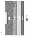
- FIG. 7 illustrates an embodiment of the device of FIG. 3 after formation of a CMOS layer and CMOS contact.
- FIG. 8 illustrates an embodiment of a CMOS layer and CMOS contact.
- FIG. 9A illustrates an embodiment of the device of FIG. 7 after formation of solar cell contacts.
- FIG. 9B illustrates an embodiment of the device of FIG. 7 after formation of solar cell contacts.
- FIG. 10 illustrates an embodiment of an autonomous IC comprising an interdigitated solar cell.
- FIG. 11 illustrates another embodiment of an autonomous IC comprising an interdigitated solar cell.
- An IC may be autonomous (i.e., self-powering, or operable without an external power supply), through integration of a solar cell into the IC; the solar cell may power the CMOS device layer of the IC.
- Autonomous ICs may be used for many applications in order to eliminate the need for a power supply to power the IC.
- forming an autonomous IC by monolithic integration of a solar cell with the CMOS device layer on the top semiconductor layer of an SOI substrate may entail epitaxial growth of a relatively thick silicon (Si) layer on the top semiconductor layer in order to enable sufficient light absorption by the solar cell.
- placing the solar cell on the top semiconductor layer of the SOI substrate may limit the area of the semiconductor material available for CMOS device fabrication.
- the thicker bottom substrate of the SOI substrate may be used as a handle substrate for formation of a solar cell, and CMOS devices may be formed on the top semiconductor layer of the SOI substrate, allowing formation of a relatively compact autonomous IC and efficient use of the SOI substrate.
- FIG. 1 illustrates an embodiment of a method 100 of forming an autonomous IC using an SOI substrate, such as substrate 200 shown in FIG. 2 .
- SOI substrate 200 includes relatively thin top semiconductor layer 201 , which may be silicon (Si) in some embodiments, an insulator layer 202 , which may be a dielectric material such as an oxide, e.g., silicon oxide (SiO 2 ), in some embodiments, and relatively thick bottom substrate 203 , which may include Si in some embodiments.
- the bottom substrate 203 may be textured or non-textured in various embodiments.
- SOI substrate 200 may be formed by any appropriate method.
- a solar cell 301 is formed using bottom substrate 203 as a handle substrate.
- Solar cell 301 may be any appropriate type of solar cell; the type of solar cell formed for solar cell 301 may be selected based on the power requirements of the finished autonomous IC.
- solar cell may include but is not limited to a single junction (single or double-emitter) solar cell, a heterojunction solar cell, or tandem solar cell, or a multijunction solar cell.
- FIGS. 4-6 show various examples of solar cells that may comprise solar cell 301 ; however, FIGS.
- solar cell 301 may be any type of solar cell that is appropriate for powering a CMOS layer of a finished autonomous IC, may include any number and type of junctions, and may be fabricated in any appropriate manner that uses bottom substrate 203 as a handle substrate.
- some or all of the steps of solar cell fabrication may occur before or during the formation of the SOI substrate.
- a doped layer (for example, any of doped layers 401 , 501 , or 601 of FIGS. 4-6 , respectively), may be formed in a bottom substrate 203 before a bonding step is performed to joint the bottom substrate 203 to top semiconductor layer 201 to form the SOI substrate 200 .
- the protective coating 302 may include an oxide, such as transparent conducting oxide (TCO) or plasma enhanced oxide deposited using chemical vapor deposition (CVD), or a nitride in some embodiments.
- TCO transparent conducting oxide
- CVD chemical vapor deposition
- FIG. 4 illustrates an embodiment of a single junction solar cell 400 that may comprise the solar cell 301 of FIG. 3 that is formed in block 101 .
- a top heavily doped Si layer 401 , a lightly doped Si layer 402 , and a bottom heavily doped Si layer 403 are formed using bottom substrate 203 of FIG. 2 .
- Layers 401 , 402 , and 403 may be crystalline Si.
- Layers 401 and 403 and may have an opposite doping type (n-type or p-type) to each other.
- Heavily doped Si layers 401 and 403 may be doped with carbon or germanium in some embodiments.
- Top heavily doped Si layer 401 is adjacent to insulating layer 202 of FIG. 3 , and protective coating 302 of FIG. 3 is formed over bottom heavily doped Si layer 403 .
- Top heavily doped Si layer 401 carries V dd for the solar cell 400 , and bottom heavily doped Si layer 403 is ground.
- FIG. 5 illustrates an embodiment of a single heterojunction solar cell 500 that may comprise the solar cell 301 of FIG. 3 that is formed in block 101 .
- a top heavily doped Si layer 501 and a lightly doped Si layer 502 are formed using bottom substrate 203 of FIG. 3 .
- Layers 501 and 502 may be crystalline Si.
- An intrinsic layer 503 of hydrogenated amorphous Si (a-Si:H) is then formed on lightly doped layer 502 , and a bottom heavily doped Si layer 504 is formed on intrinsic a-Si:H layer 503 .
- Bottom heavily doped Si layer 504 may be a-Si:H or polysilicon in various embodiments.
- Layers 501 and 504 may have an opposite doping type (n-type or p-type) to each other.
- heavily doped Si layers 501 and 504 may be doped with carbon or germanium in some embodiments.
- Top heavily doped Si layer 501 is adjacent to insulating layer 202 of FIG. 3 , and protective coating 302 of FIG. 3 is formed over bottom heavily doped Si layer 504 .
- Top heavily doped Si layer 501 carries V dd for the solar cell 500 , and bottom heavily doped Si layer 504 is ground.
- crystalline layers 501 and 502 may first be formed using bottom substrate 203 , and protective coating 302 may be formed over crystalline layer 502 . Then, a CMOS layer (discussed below with respect to FIG. 7 ) may then be formed using top semiconductor layer 201 . After formation of the CMOS layer, the protective layer 302 may be removed, amorphous layers 503 and 504 may be formed on crystalline layer 502 , and another protective layer (which may be an antireflective coating (ARC), TCO, or nitride in various embodiments) may then be formed on amorphous layer 504 .
- ARC antireflective coating
- FIG. 6 illustrates an embodiment of a tandem solar cell 600 that may comprise the solar cell 301 of FIG. 3 that is formed in block 101 .
- Tandem cell 600 includes a top heterojunction solar cell (including layers 601 - 603 ) in conjunction with an amorphous photovoltaic (PV) cell (including layers 605 - 607 ) joined by a tunneling diode (layer 604 ).
- a top heavily doped Si layer 601 and a lightly doped Si layer 602 are formed using bottom substrate 203 of FIG. 3 .
- Layers 601 and 602 may each be crystalline Si.
- a heavily doped amorphous layer 603 of a-Si:H is formed on lightly doped layer 602 .
- Amorphous layer 603 may have a doping type (n-type or p-type) that is opposite that of layer 601 .
- Tunneling diode layer 604 which may be TCO, is formed on amorphous layer 603 .
- a heavily doped a-Si:H layer 605 is formed on tunneling diode layer 604
- an intrinsic a-Si:H layer 606 is formed on heavily doped layer a-Si:H 605
- a heavily doped a-Si:H layer 607 is formed on intrinsic layer 606 .
- Layer 605 may have the same doping type (n-type or p-type) as layers 601 and 602
- layer 607 may have the same doping type (n-type or p-type) as layer 603
- Positively doped layers 601 , 603 , 605 , and 607 may be doped with carbon or germanium in some embodiments.
- Top heavily doped Si layer 601 is adjacent to insulating layer 202 of FIG. 3 , and protective coating 302 of FIG. 3 is formed over bottom heavily doped a-Si:H layer 607 .
- Top heavily doped Si layer 601 carries V dd for the solar cell 600
- bottom heavily doped a-Si:H layer 607 is ground.
- CMOS device layer 701 may include any appropriate number, type, and configuration of CMOS devices, including but not limited to field effect transistors (FETs).
- FETs field effect transistors
- CMOS device layer 701 is contacted by a CMOS contact 702 .
- Via 703 is also formed through insulating layer 202 to connect the V dd (e.g., layer 401 of FIG. 1 , layer 501 of FIG. 5 , or layer 601 of FIG.
- CMOS device layer 701 acts to protect solar cell 301 during formation of CMOS layer 701 .
- Protective layer 302 acts to protect solar cell 301 during formation of CMOS layer 701 .
- Contact 702 and via 703 are shown for illustrative purposes only; a CMOS layer 701 may include any appropriate configuration of contacts and vias.
- CMOS contact 702 and via 703 may comprise a metal such as copper or polysilicon in various embodiments.
- CMOS layer 701 may be formed separately in a semiconductor layer (which acts as top semiconductor layer 201 ), and then bonded to a solar cell 301 formed in a bottom substrate (which acts as bottom substrate 203 ) using a dielectric glue layer (which acts as insulating layer 202 ).
- Contact hole(s), such as for via 703 may be formed in the dielectric glue layer between the bonded CMOS layer 701 and solar cell 301 .
- FIG. 8 shows an illustrative embodiment of a CMOS device layer 800 that may comprise the CMOS device layer 701 formed in block 103 .
- Shallow trench isolation (STI) regions 801 A-C are formed in semiconductor layer 201 of the SOI substrate. STI regions 801 A-C act to insulate CMOS devices from one another, and may be filled with an oxide material in some embodiments.
- Doped source and drain regions 802 A-D are also formed in semiconductor layer 201 , on either side of undoped channel regions 803 A-B. Source and drain regions 802 A-D may be either n-type or p-type.
- a first FET device includes source and drain regions 802 A-B, channel region 803 A, and gate 804 A; a second FET device includes source and drain regions 802 C-D, channel region 803 B, and gate 804 B.
- Gates 804 A-B may include a high-k dielectric layer and/or a gate metal layer, and may include a nitride spacer located adjacent to the gates 804 A-B.
- CMOS contact 702 (also shown in FIG. 7 ) provides a gate voltage to FET gates 804 A-B.
- CMOS layer 800 of FIG. 8 is shown for illustrative purposes only; the CMOS layer 701 of FIG. 7 may include any number, type, and configuration of CMOS devices.
- CMOS device layer 701 including CMOS contact 702 and via 703 , in block 103 , in block 104 , one or more contacts to solar cell 301 are formed, and the contacts to solar cell 301 are connected to CMOS contact 702 , allowing solar cell 301 to power CMOS device layer 701 , resulting in autonomous ICs 900 A-B such as are shown in FIGS. 9A-B .
- there may be additional processing of the solar cell 301 (such as is discussed above with respect to FIG. 5 ) after completion of CMOS layer 701 and before formation of the solar cell contacts.
- FIG. 5 there may be additional processing of the solar cell 301 (such as is discussed above with respect to FIG. 5 ) after completion of CMOS layer 701 and before formation of the solar cell contacts.
- protective layer 302 is a non-conducting material, so solar cell contacts 901 A-B are formed by recessing protective layer 302 such that solar cell contacts 901 A-B are directly contacted to solar cell 301 . Electrical connections, such as example electrical connection 903 , are then formed from solar cell contacts 901 A-B to CMOS contact 702 , allowing solar cell 301 to power CMOS layer 701 .
- protective layer 302 is a conducting material, such as TCO, and solar cell contacts 902 A-C are formed on protective layer 302 .
- Solar cell contacts 901 A-B and solar cell contacts 902 A-C may be a metal, such as copper, or polysilicon in various embodiments.
- Solar cell contacts 901 A-B of FIGS. 9 A and 902 A-C of FIG. 9B are shown for illustrative purposes only; an autonomous IC may include any appropriate number and configuration of solar cell contacts.
- protective layer 302 may be removed, and the solar cell contacts may be formed directly on solar cell 301 . In operation, solar cell 301 receives solar energy, and transforms the solar energy into electrical energy to power CMOS layer 701 .
- FIG. 10 illustrates an embodiment of an autonomous IC 1000 that may be formed using the method 100 of FIG. 1 , in which the solar cell 301 has an interdigitated configuration.
- Solar cell 301 includes heavily doped regions 1003 a - b and 1004 a - b in lightly doped region 1002 .
- Heavily doped regions 1003 a - b and 1004 a - b are each adjacent to insulator layer 202 .
- Heavily doped regions 1003 a - b may have a doping type (n-type or p-type) that is opposite to a doping type of heavily doped regions 1004 a - b
- lightly doped region 1002 may have a doping type (n-type or p-type) that is the same as that of heavily doped regions 1004 a - b
- Heavily doped region 1003 a supplies ground to the CMOS device layer 701 through via 1005 , which is formed in insulator layer 202
- heavily doped region 1104 b supplies V dd to CMOS device layer 701 through via 703 .
- the bottom of solar cell 301 is electrically connected to CMOS contact 702 by an electrical connection such as example electrical connection 1006 to power the CMOS device layer 701 in operation.
- FIG. 11 illustrates another embodiment of an autonomous IC 1100 that may be formed using the method 100 of FIG. 1 in which solar cell 301 has an interdigitated configuration.
- Heavily doped regions 1103 a - b and 1104 are located in lightly doped region 1102 and separated by insulating spacers 1105 , which may comprise the same material as insulating layer 202 .
- Heavily doped region 1104 supplies ground to the CMOS device layer 701 through via 1114 , which is formed in insulator layer 202 , and heavily doped regions 1103 a - b supply V dd to CMOS device layer 701 through vias 1113 .
- the bottom of solar cell 301 is electrically connected to CMOS contact 702 by an electrical connection such as example electrical connection 1106 to power the CMOS device layer 701 in operation.
- the technical effects and benefits of exemplary embodiments include a relatively compact autonomous IC that makes efficient use of an SOI substrate.
Landscapes
- Engineering & Computer Science (AREA)
- Physics & Mathematics (AREA)
- Power Engineering (AREA)
- Microelectronics & Electronic Packaging (AREA)
- Condensed Matter Physics & Semiconductors (AREA)
- Electromagnetism (AREA)
- General Physics & Mathematics (AREA)
- Computer Hardware Design (AREA)
- Sustainable Energy (AREA)
- Life Sciences & Earth Sciences (AREA)
- Sustainable Development (AREA)
- Manufacturing & Machinery (AREA)
- Metal-Oxide And Bipolar Metal-Oxide Semiconductor Integrated Circuits (AREA)
- Photovoltaic Devices (AREA)
- Thin Film Transistor (AREA)
Abstract
Description
Claims (9)
Priority Applications (1)
| Application Number | Priority Date | Filing Date | Title |
|---|---|---|---|
| US14/199,206 US8969992B2 (en) | 2010-11-15 | 2014-03-06 | Autonomous integrated circuits |
Applications Claiming Priority (2)
| Application Number | Priority Date | Filing Date | Title |
|---|---|---|---|
| US12/946,216 US20120118383A1 (en) | 2010-11-15 | 2010-11-15 | Autonomous Integrated Circuit |
| US14/199,206 US8969992B2 (en) | 2010-11-15 | 2014-03-06 | Autonomous integrated circuits |
Related Parent Applications (1)
| Application Number | Title | Priority Date | Filing Date |
|---|---|---|---|
| US12/946,216 Division US20120118383A1 (en) | 2010-11-15 | 2010-11-15 | Autonomous Integrated Circuit |
Publications (2)
| Publication Number | Publication Date |
|---|---|
| US20140183686A1 US20140183686A1 (en) | 2014-07-03 |
| US8969992B2 true US8969992B2 (en) | 2015-03-03 |
Family
ID=46046689
Family Applications (2)
| Application Number | Title | Priority Date | Filing Date |
|---|---|---|---|
| US12/946,216 Abandoned US20120118383A1 (en) | 2010-11-15 | 2010-11-15 | Autonomous Integrated Circuit |
| US14/199,206 Active US8969992B2 (en) | 2010-11-15 | 2014-03-06 | Autonomous integrated circuits |
Family Applications Before (1)
| Application Number | Title | Priority Date | Filing Date |
|---|---|---|---|
| US12/946,216 Abandoned US20120118383A1 (en) | 2010-11-15 | 2010-11-15 | Autonomous Integrated Circuit |
Country Status (1)
| Country | Link |
|---|---|
| US (2) | US20120118383A1 (en) |
Cited By (1)
| Publication number | Priority date | Publication date | Assignee | Title |
|---|---|---|---|---|
| US20160343696A1 (en) * | 2015-05-21 | 2016-11-24 | Freescale Semiconductor, Inc. | Solar cell powered integrated circuit device and method therefor |
Families Citing this family (13)
| Publication number | Priority date | Publication date | Assignee | Title |
|---|---|---|---|---|
| US20120118383A1 (en) | 2010-11-15 | 2012-05-17 | International Business Machines Corporation | Autonomous Integrated Circuit |
| US9147701B2 (en) * | 2011-09-22 | 2015-09-29 | Raytheon Company | Monolithic InGaN solar cell power generation with integrated efficient switching DC-DC voltage convertor |
| US8906779B2 (en) | 2012-03-30 | 2014-12-09 | International Business Machines Corporation | Solar-powered energy-autonomous silicon-on-insulator device |
| US8980737B2 (en) | 2012-05-24 | 2015-03-17 | International Business Machines Corporation | Methods of forming contact regions using sacrificial layers |
| US9064924B2 (en) | 2012-05-24 | 2015-06-23 | International Business Machines Corporation | Heterojunction bipolar transistors with intrinsic interlayers |
| US9093548B2 (en) * | 2012-06-06 | 2015-07-28 | International Business Machines Corporation | Thin film hybrid junction field effect transistor |
| US9087705B2 (en) | 2013-06-05 | 2015-07-21 | International Business Machines Corporation | Thin-film hybrid complementary circuits |
| US9230940B2 (en) | 2013-09-13 | 2016-01-05 | Globalfoundries Inc. | Three-dimensional chip stack for self-powered integrated circuit |
| FR3012669B1 (en) | 2013-10-29 | 2017-01-13 | Commissariat Energie Atomique | METHOD FOR MANUFACTURING A DEVICE COMPRISING AN INTEGRATED CIRCUIT AND PHOTOVOLTAIC CELLS |
| US9530921B2 (en) | 2014-10-02 | 2016-12-27 | International Business Machines Corporation | Multi-junction solar cell |
| US10475738B2 (en) * | 2016-12-27 | 2019-11-12 | United Microelectronics Corp. | Multi-threshold voltage semiconductor device |
| US20180358258A1 (en) * | 2017-06-09 | 2018-12-13 | Texas Instruments Incorporated | Single mask level forming both top-side-contact and isolation trenches |
| US10115837B1 (en) * | 2017-09-28 | 2018-10-30 | Globalfoundries Singapore Pte. Ltd. | Integrated circuits with solar cells and methods for producing the same |
Citations (20)
| Publication number | Priority date | Publication date | Assignee | Title |
|---|---|---|---|---|
| US5616185A (en) | 1995-10-10 | 1997-04-01 | Hughes Aircraft Company | Solar cell with integrated bypass diode and method |
| US6864414B2 (en) | 2001-10-24 | 2005-03-08 | Emcore Corporation | Apparatus and method for integral bypass diode in solar cells |
| US20050104089A1 (en) | 2002-02-05 | 2005-05-19 | Engelmann Michael G. | Visible/near infrared image sensor |
| US7098394B2 (en) | 2001-05-15 | 2006-08-29 | Pharmaseq, Inc. | Method and apparatus for powering circuitry with on-chip solar cells within a common substrate |
| US20060267054A1 (en) | 2002-02-05 | 2006-11-30 | Peter Martin | Image sensor with microcrystalline germanium photodiode layer |
| US20080308143A1 (en) | 2007-06-15 | 2008-12-18 | Translucent Photonics, Inc. | Thin Film Semi-Conductor-on-Glass Solar Cell Devices |
| US20090007965A1 (en) * | 2004-05-11 | 2009-01-08 | Georgia Tech Research Corporation | Solar cell device having amorphous silicon layers |
| US20090009675A1 (en) | 2007-01-25 | 2009-01-08 | Au Optronics Corporation | Photovoltaic Cells of Si-Nanocrystals with Multi-Band Gap and Applications in a Low Temperature Polycrystalline Silicon Thin Film Transistor Panel |
| US20100096447A1 (en) | 2007-03-09 | 2010-04-22 | Sunghoon Kwon | Optical identification tag, reader and system |
| US20100243058A1 (en) * | 2007-11-02 | 2010-09-30 | Kaneka Corporation | Thin-film photoelectric conversion device |
| US20110086246A1 (en) | 2008-06-09 | 2011-04-14 | Nxp B.V. | Semiconductor device comprising a solar cell, method of manufacturing a semiconductor device and apparatus comprising a semiconductor device |
| US7928317B2 (en) | 2006-06-05 | 2011-04-19 | Translucent, Inc. | Thin film solar cell |
| US20110277820A1 (en) * | 2010-05-17 | 2011-11-17 | The Boeing Company | Solar Cell Structure Including A Silicon Carrier Containing A By-Pass Diode |
| US20110277808A1 (en) | 2010-03-22 | 2011-11-17 | Scannanotek Oy | Mems solar cell device and array |
| US20120040490A1 (en) * | 2008-12-10 | 2012-02-16 | Applied Materials Italia S.R.L. | Enhanced vision system for screen printing pattern alignment |
| US20120118383A1 (en) | 2010-11-15 | 2012-05-17 | International Business Machines Corporation | Autonomous Integrated Circuit |
| US20120126247A1 (en) | 2010-08-25 | 2012-05-24 | Texas Instruments Incorporated | Self-powered integrated circuit with multi-junction photovoltaic cell |
| US20120126298A1 (en) | 2010-08-25 | 2012-05-24 | Texas Instruments Incorporated | Self-powered integrated circuit with photovoltaic cell |
| US20120312353A1 (en) | 2009-07-17 | 2012-12-13 | Universitaet Ulm | Semiconductor component having diamond-containing electrodes and use thereof |
| US20130074907A1 (en) | 2011-09-22 | 2013-03-28 | Jeffrey H. Saunders | MONOLITHIC InGaN SOLAR CELL POWER GENERATION WITH INTEGRATED EFFICIENT SWITCHING DC-DC VOLTAGE CONVERTOR |
-
2010
- 2010-11-15 US US12/946,216 patent/US20120118383A1/en not_active Abandoned
-
2014
- 2014-03-06 US US14/199,206 patent/US8969992B2/en active Active
Patent Citations (23)
| Publication number | Priority date | Publication date | Assignee | Title |
|---|---|---|---|---|
| US5616185A (en) | 1995-10-10 | 1997-04-01 | Hughes Aircraft Company | Solar cell with integrated bypass diode and method |
| US7098394B2 (en) | 2001-05-15 | 2006-08-29 | Pharmaseq, Inc. | Method and apparatus for powering circuitry with on-chip solar cells within a common substrate |
| US6864414B2 (en) | 2001-10-24 | 2005-03-08 | Emcore Corporation | Apparatus and method for integral bypass diode in solar cells |
| US20050104089A1 (en) | 2002-02-05 | 2005-05-19 | Engelmann Michael G. | Visible/near infrared image sensor |
| US20060267054A1 (en) | 2002-02-05 | 2006-11-30 | Peter Martin | Image sensor with microcrystalline germanium photodiode layer |
| US7276749B2 (en) | 2002-02-05 | 2007-10-02 | E-Phocus, Inc. | Image sensor with microcrystalline germanium photodiode layer |
| US7436038B2 (en) | 2002-02-05 | 2008-10-14 | E-Phocus, Inc | Visible/near infrared image sensor array |
| US20090007965A1 (en) * | 2004-05-11 | 2009-01-08 | Georgia Tech Research Corporation | Solar cell device having amorphous silicon layers |
| US7928317B2 (en) | 2006-06-05 | 2011-04-19 | Translucent, Inc. | Thin film solar cell |
| US20090009675A1 (en) | 2007-01-25 | 2009-01-08 | Au Optronics Corporation | Photovoltaic Cells of Si-Nanocrystals with Multi-Band Gap and Applications in a Low Temperature Polycrystalline Silicon Thin Film Transistor Panel |
| US20100096447A1 (en) | 2007-03-09 | 2010-04-22 | Sunghoon Kwon | Optical identification tag, reader and system |
| US20080308143A1 (en) | 2007-06-15 | 2008-12-18 | Translucent Photonics, Inc. | Thin Film Semi-Conductor-on-Glass Solar Cell Devices |
| US8071872B2 (en) | 2007-06-15 | 2011-12-06 | Translucent Inc. | Thin film semi-conductor-on-glass solar cell devices |
| US20100243058A1 (en) * | 2007-11-02 | 2010-09-30 | Kaneka Corporation | Thin-film photoelectric conversion device |
| US20110086246A1 (en) | 2008-06-09 | 2011-04-14 | Nxp B.V. | Semiconductor device comprising a solar cell, method of manufacturing a semiconductor device and apparatus comprising a semiconductor device |
| US20120040490A1 (en) * | 2008-12-10 | 2012-02-16 | Applied Materials Italia S.R.L. | Enhanced vision system for screen printing pattern alignment |
| US20120312353A1 (en) | 2009-07-17 | 2012-12-13 | Universitaet Ulm | Semiconductor component having diamond-containing electrodes and use thereof |
| US20110277808A1 (en) | 2010-03-22 | 2011-11-17 | Scannanotek Oy | Mems solar cell device and array |
| US20110277820A1 (en) * | 2010-05-17 | 2011-11-17 | The Boeing Company | Solar Cell Structure Including A Silicon Carrier Containing A By-Pass Diode |
| US20120126247A1 (en) | 2010-08-25 | 2012-05-24 | Texas Instruments Incorporated | Self-powered integrated circuit with multi-junction photovoltaic cell |
| US20120126298A1 (en) | 2010-08-25 | 2012-05-24 | Texas Instruments Incorporated | Self-powered integrated circuit with photovoltaic cell |
| US20120118383A1 (en) | 2010-11-15 | 2012-05-17 | International Business Machines Corporation | Autonomous Integrated Circuit |
| US20130074907A1 (en) | 2011-09-22 | 2013-03-28 | Jeffrey H. Saunders | MONOLITHIC InGaN SOLAR CELL POWER GENERATION WITH INTEGRATED EFFICIENT SWITCHING DC-DC VOLTAGE CONVERTOR |
Non-Patent Citations (2)
| Title |
|---|
| S. Bermejo et al., Prog. Photovolt: Res. Appl., 2005, pp. 617-625, vol. 13, IEEE. |
| T.I. Chappell et al., IEEE Trans Elec. Dev., 1979, pp. 1091-1097, vol. ED-26, IEEE. |
Cited By (2)
| Publication number | Priority date | Publication date | Assignee | Title |
|---|---|---|---|---|
| US20160343696A1 (en) * | 2015-05-21 | 2016-11-24 | Freescale Semiconductor, Inc. | Solar cell powered integrated circuit device and method therefor |
| US10008447B2 (en) * | 2015-05-21 | 2018-06-26 | Nxp Usa, Inc. | Solar cell powered integrated circuit device and method therefor |
Also Published As
| Publication number | Publication date |
|---|---|
| US20120118383A1 (en) | 2012-05-17 |
| US20140183686A1 (en) | 2014-07-03 |
Similar Documents
| Publication | Publication Date | Title |
|---|---|---|
| US8969992B2 (en) | Autonomous integrated circuits | |
| US9570485B2 (en) | Solar-powered energy-autonomous silicon-on-insulator device | |
| TWI433305B (en) | Soi device and method for its fabrication | |
| TWI534864B (en) | Soi finfet with recessed merged fins and liner for enhanced stress coupling | |
| US11139215B2 (en) | Hybrid gate stack integration for stacked vertical transport field-effect transistors | |
| US9466651B2 (en) | Flexible active matrix display | |
| US10128452B2 (en) | Hybrid junction field-effect transistor and active matrix structure | |
| US11011662B2 (en) | Field-effect photovoltaic elements | |
| US9721951B2 (en) | Semiconductor device using Ge channel and manufacturing method thereof | |
| US8680628B2 (en) | Raised source/drain field effect transistor | |
| US8344468B2 (en) | Photovoltaic device with lateral P-I-N light-sensitive diodes | |
| CN101777565B (en) | Self-powered low power consumption integrated circuit chip and preparation method thereof | |
| CN103824857A (en) | Semiconductor structure including semiconductor-on-insulator region and bulk region, and method for the formation thereof | |
| CN101719496A (en) | Self-power integrated circuit chip and production method thereof | |
| CN109524355B (en) | Structure and forming method of semiconductor device | |
| CN103779416B (en) | The power MOSFET device of a kind of low VF and manufacture method thereof | |
| CN109560065B (en) | Semiconductor device structure with body contact and forming method | |
| US20120056273A1 (en) | Semiconductor device and method of manufacturing the same | |
| US11764207B2 (en) | Diode structures of stacked devices and methods of forming the same | |
| CN109545785B (en) | Semiconductor device structure and preparation method | |
| CN115172393A (en) | Short wave infrared imaging chip and preparation method thereof | |
| CN113594161A (en) | Semiconductor device and method for manufacturing the same |
Legal Events
| Date | Code | Title | Description |
|---|---|---|---|
| AS | Assignment |
Owner name: INTERNATIONAL BUSINESS MACHINES CORPORATION, NEW Y Free format text: ASSIGNMENT OF ASSIGNORS INTEREST;ASSIGNORS:BEDELL, STEPHEN W.;SOSA CORTES, NORMA E.;HAENSCH, WILFRIED E.;AND OTHERS;SIGNING DATES FROM 20140122 TO 20140226;REEL/FRAME:032368/0179 |
|
| STCF | Information on status: patent grant |
Free format text: PATENTED CASE |
|
| MAFP | Maintenance fee payment |
Free format text: PAYMENT OF MAINTENANCE FEE, 4TH YEAR, LARGE ENTITY (ORIGINAL EVENT CODE: M1551) Year of fee payment: 4 |
|
| MAFP | Maintenance fee payment |
Free format text: PAYMENT OF MAINTENANCE FEE, 8TH YEAR, LARGE ENTITY (ORIGINAL EVENT CODE: M1552); ENTITY STATUS OF PATENT OWNER: LARGE ENTITY Year of fee payment: 8 |