US8943292B2 - System and method for memory array access with fast address decoder - Google Patents
System and method for memory array access with fast address decoder Download PDFInfo
- Publication number
- US8943292B2 US8943292B2 US11/552,817 US55281706A US8943292B2 US 8943292 B2 US8943292 B2 US 8943292B2 US 55281706 A US55281706 A US 55281706A US 8943292 B2 US8943292 B2 US 8943292B2
- Authority
- US
- United States
- Prior art keywords
- bits
- wordline
- pgzo
- lsb
- msb
- Prior art date
- Legal status (The legal status is an assumption and is not a legal conclusion. Google has not performed a legal analysis and makes no representation as to the accuracy of the status listed.)
- Active, expires
Links
- 238000000034 method Methods 0.000 title claims abstract description 25
- 238000003491 array Methods 0.000 claims description 16
- 238000012545 processing Methods 0.000 claims description 4
- 239000000872 buffer Substances 0.000 abstract description 7
- 238000013507 mapping Methods 0.000 description 41
- 238000010586 diagram Methods 0.000 description 16
- 230000008569 process Effects 0.000 description 14
- 230000006870 function Effects 0.000 description 10
- 239000000463 material Substances 0.000 description 3
- 238000004891 communication Methods 0.000 description 2
- 238000004590 computer program Methods 0.000 description 2
- 238000012986 modification Methods 0.000 description 2
- 230000004048 modification Effects 0.000 description 2
- 230000004913 activation Effects 0.000 description 1
- 238000013479 data entry Methods 0.000 description 1
- 230000000694 effects Effects 0.000 description 1
- 230000000977 initiatory effect Effects 0.000 description 1
- 230000003287 optical effect Effects 0.000 description 1
- 230000002093 peripheral effect Effects 0.000 description 1
Images


Classifications
-
- G—PHYSICS
- G06—COMPUTING; CALCULATING OR COUNTING
- G06F—ELECTRIC DIGITAL DATA PROCESSING
- G06F9/00—Arrangements for program control, e.g. control units
- G06F9/06—Arrangements for program control, e.g. control units using stored programs, i.e. using an internal store of processing equipment to receive or retain programs
- G06F9/30—Arrangements for executing machine instructions, e.g. instruction decode
- G06F9/34—Addressing or accessing the instruction operand or the result ; Formation of operand address; Addressing modes
- G06F9/355—Indexed addressing
-
- G—PHYSICS
- G06—COMPUTING; CALCULATING OR COUNTING
- G06F—ELECTRIC DIGITAL DATA PROCESSING
- G06F9/00—Arrangements for program control, e.g. control units
- G06F9/06—Arrangements for program control, e.g. control units using stored programs, i.e. using an internal store of processing equipment to receive or retain programs
- G06F9/30—Arrangements for executing machine instructions, e.g. instruction decode
- G06F9/34—Addressing or accessing the instruction operand or the result ; Formation of operand address; Addressing modes
- G06F9/345—Addressing or accessing the instruction operand or the result ; Formation of operand address; Addressing modes of multiple operands or results
Landscapes
- Engineering & Computer Science (AREA)
- Software Systems (AREA)
- Theoretical Computer Science (AREA)
- Physics & Mathematics (AREA)
- General Engineering & Computer Science (AREA)
- General Physics & Mathematics (AREA)
- Memory System Of A Hierarchy Structure (AREA)
- Executing Machine-Instructions (AREA)
Abstract
Description
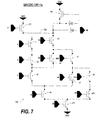
| Macro Input | |||
| (see FIG. 7) | PGZO Value Mapped to Input | ||
| a | Exclusive NOR (XNOR) of MSB | ||
| aa | Exclusive OR (XOR) of MSB | ||
| b | AND of inverted MSB − 1 | ||
| bb | AND of MSB − 1 | ||
| bbb | XOR of MSB − 1 | ||
| c | AND of inverted LSB + 1 | ||
| cc | AND of MSB − 1 | ||
| ccc | XOR of LSB + 1 | ||
| d | AND of inverted LSB | ||
| dd | OR of LSB | ||
| Macro Input | |||
| (see FIG. 7) | PGZO Value Mapped to Input | ||
| a | Exclusive NOR (XNOR) of MSB | ||
| aa | Exclusive OR (XOR) of MSB | ||
| b | AND of inverted MSB − 1 | ||
| bb | AND of MSB − 1 | ||
| bbb | XOR of MSB − 1 | ||
| c | AND of inverted LSB + 1 | ||
| cc | AND of MSB − 1 | ||
| ccc | XOR of LSB + 1 | ||
| d | Inverted AND (NAND) of LSB | ||
| dd | AND of LSB | ||
| Macro Input | |||
| (see FIG. 8) | PGZO Value Mapped to Input | ||
| a | Exclusive NOR (XNOR) of MSB | ||
| aa | Exclusive OR (XOR) of MSB | ||
| b | AND of inverted MSB − 1 | ||
| bb | AND of MSB − 1 | ||
| bbb | XOR of MSB − 1 | ||
| c | XOR of LSB + 1 | ||
| cc | AND of inverted LSB + 1 | ||
| ccc | AND of LSB + 1 | ||
| d | AND of inverted LSB | ||
| dd | OR of LSB | ||
| Macro Input | |||
| (see FIG. 8) | PGZO Value Mapped to Input | ||
| a | Exclusive NOR (XNOR) of MSB | ||
| aa | Exclusive OR (XOR) of MSB | ||
| b | AND of inverted MSB − 1 | ||
| bb | AND of MSB − 1 | ||
| bbb | XOR of MSB − 1 | ||
| c | XOR of LSB + 1 | ||
| cc | AND of inverted LSB + 1 | ||
| ccc | AND of LSB + 1 | ||
| d | Inverted AND (NAND) of LSB | ||
| dd | AND of LSB | ||
| Macro Input | |||
| (see FIG. 8) | PGZO Value Mapped to Input | ||
| a | Exclusive OR (XOR) of MSB | ||
| aa | Exclusive NOR (XNOR) of MSB | ||
| b | AND of MSB − 1 | ||
| bb | AND of inverted MSB − 1 | ||
| bbb | XOR of MSB − 1 | ||
| c | XOR of LSB + 1 | ||
| cc | AND of LSB + 1 | ||
| ccc | AND of inverted LSB + 1 | ||
| d | OR of LSB | ||
| dd | AND of inverted LSB | ||
| Macro Input | |||
| (see FIG. 8) | PGZO Value Mapped to Input | ||
| a | Exclusive OR (XOR) of MSB | ||
| aa | Exclusive NOR (XNOR) of MSB | ||
| b | AND of MSB − 1 | ||
| bb | AND of inverted MSB − 1 | ||
| bbb | XOR of MSB − 1 | ||
| c | XOR of LSB + 1 | ||
| cc | AND of LSB + 1 | ||
| ccc | AND of inverted LSB + 1 | ||
| d | AND of LSB | ||
| dd | Inverted AND (NAND) of LSB | ||
| Macro Input | |||
| (see FIG. 7) | PGZO Value Mapped to Input | ||
| a | Exclusive OR (XOR) of MSB | ||
| aa | Exclusive NOR (XNOR) of MSB | ||
| b | AND of MSB − 1 | ||
| bb | AND of inverted MSB − 1 | ||
| bbb | XOR of MSB − 1 | ||
| c | AND of LSB + 1 | ||
| cc | AND of inverted LSB + 1 | ||
| ccc | XOR of LSB + 1 | ||
| d | OR of LSB | ||
| dd | AND of inverted LSB | ||
| Macro Input | |||
| (see FIG. 7) | PGZO Value Mapped to Input | ||
| a | Exclusive OR (XOR) of MSB | ||
| aa | Exclusive NOR (XNOR) of MSB | ||
| b | AND of MSB − 1 | ||
| bb | AND of inverted MSB − 1 | ||
| bbb | XOR of MSB − 1 | ||
| c | AND of LSB + 1 | ||
| cc | AND of inverted LSB + 1 | ||
| ccc | XOR of LSB + 1 | ||
| d | AND of LSB | ||
| dd | Inverted AND (NAND) of LSB | ||
| Macro Input | |||
| (see FIG. 7) | PGZO Value Mapped to Input | ||
| a | Exclusive OR (XOR) of MSB | ||
| aa | Exclusive NOR (XNOR) of MSB | ||
| b | AND of inverted MSB − 1 | ||
| bb | AND of MSB − 1 | ||
| bbb | XOR of MSB − 1 | ||
| c | AND of inverted LSB + 1 | ||
| cc | AND of LSB + 1 | ||
| ccc | XOR of LSB + 1 | ||
| d | AND of inverted LSB | ||
| dd | OR of LSB | ||
| Macro Input | |||
| (see FIG. 7) | PGZO Value Mapped to Input | ||
| a | Exclusive OR (XOR) of MSB | ||
| aa | Exclusive NOR (XNOR) of MSB | ||
| b | AND of inverted MSB − 1 | ||
| bb | AND of MSB − 1 | ||
| bbb | XOR of MSB − 1 | ||
| c | AND of inverted LSB + 1 | ||
| cc | AND of LSB + 1 | ||
| ccc | XOR of LSB + 1 | ||
| d | Inverted AND (NAND) of LSB | ||
| dd | AND of LSB | ||
| Macro Input | |||
| (see FIG. 8) | PGZO Value Mapped to Input | ||
| a | Exclusive OR (XOR) of MSB | ||
| aa | Exclusive NOR (XNOR) of MSB | ||
| b | AND of inverted MSB − 1 | ||
| bb | AND of MSB − 1 | ||
| bbb | XOR of MSB − 1 | ||
| c | XOR of LSB + 1 | ||
| cc | AND of inverted LSB + 1 | ||
| ccc | AND of LSB + 1 | ||
| d | AND of inverted LSB | ||
| dd | OR of LSB | ||
| Macro Input | |||
| (see FIG. 8) | PGZO Value Mapped to Input | ||
| a | Exclusive OR (XOR) of MSB | ||
| aa | Exclusive NOR (XNOR) of MSB | ||
| b | AND of inverted MSB − 1 | ||
| bb | AND of MSB − 1 | ||
| bbb | XOR of MSB − 1 | ||
| c | XOR of LSB + 1 | ||
| cc | AND of inverted LSB + 1 | ||
| ccc | AND of LSB + 1 | ||
| d | Inverted AND of LSB | ||
| dd | AND of LSB | ||
| Macro Input | |||
| (see FIG. 8) | PGZO Value Mapped to Input | ||
| a | Exclusive NOR (XNOR) of MSB | ||
| aa | Exclusive OR (XOR) of MSB | ||
| b | AND of MSB − 1 | ||
| bb | AND of inverted MSB − 1 | ||
| bbb | XOR of MSB − 1 | ||
| c | XOR of LSB + 1 | ||
| cc | AND of LSB + 1 | ||
| ccc | AND of inverted LSB + 1 | ||
| d | OR of LSB | ||
| dd | AND of inverted LSB | ||
| Macro Input | |||
| (see FIG. 8) | PGZO Value Mapped to Input | ||
| a | Exclusive NOR (XNOR) of MSB | ||
| aa | Exclusive OR (XOR) of MSB | ||
| b | AND of MSB − 1 | ||
| bb | AND of inverted MSB − 1 | ||
| bbb | XOR of MSB − 1 | ||
| c | XOR of LSB + 1 | ||
| cc | AND of LSB + 1 | ||
| ccc | AND of inverted LSB + 1 | ||
| d | AND of LSB | ||
| dd | Inverted AND (NAND) of LSB | ||
| Macro Input | |||
| (see FIG. 7) | PGZO Value Mapped to Input | ||
| a | Exclusive NOR (XNOR) of MSB | ||
| aa | Exclusive OR (XOR) of MSB | ||
| b | AND of MSB − 1 | ||
| bb | AND of inverted MSB − 1 | ||
| bbb | XOR of MSB − 1 | ||
| c | AND of LSB + 1 | ||
| cc | AND of inverted LSB + 1 | ||
| ccc | XOR of LSB + 1 | ||
| d | OR of LSB | ||
| dd | AND of inverted LSB | ||
| Macro Input | |||
| (see FIG. 7) | PGZO Value Mapped to Input | ||
| a | Exclusive NOR (XNOR) of MSB | ||
| aa | Exclusive OR (XOR) of MSB | ||
| b | AND of MSB − 1 | ||
| bb | AND of inverted MSB − 1 | ||
| bbb | XOR of MSB − 1 | ||
| c | AND of LSB + 1 | ||
| cc | AND of inverted LSB + 1 | ||
| ccc | XOR of LSB + 1 | ||
| d | AND of LSB | ||
| dd | Inverted AND (NAND) of LSB | ||
Claims (6)
Priority Applications (1)
| Application Number | Priority Date | Filing Date | Title |
|---|---|---|---|
| US11/552,817 US8943292B2 (en) | 2005-10-25 | 2006-10-25 | System and method for memory array access with fast address decoder |
Applications Claiming Priority (2)
| Application Number | Priority Date | Filing Date | Title |
|---|---|---|---|
| US11/257,932 US7669034B2 (en) | 2005-10-25 | 2005-10-25 | System and method for memory array access with fast address decoder |
| US11/552,817 US8943292B2 (en) | 2005-10-25 | 2006-10-25 | System and method for memory array access with fast address decoder |
Related Parent Applications (1)
| Application Number | Title | Priority Date | Filing Date |
|---|---|---|---|
| US11/257,932 Continuation-In-Part US7669034B2 (en) | 2005-10-25 | 2005-10-25 | System and method for memory array access with fast address decoder |
Publications (2)
| Publication Number | Publication Date |
|---|---|
| US20070094480A1 US20070094480A1 (en) | 2007-04-26 |
| US8943292B2 true US8943292B2 (en) | 2015-01-27 |
Family
ID=37968342
Family Applications (2)
| Application Number | Title | Priority Date | Filing Date |
|---|---|---|---|
| US11/257,932 Active 2026-06-03 US7669034B2 (en) | 2005-10-25 | 2005-10-25 | System and method for memory array access with fast address decoder |
| US11/552,817 Active 2029-04-29 US8943292B2 (en) | 2005-10-25 | 2006-10-25 | System and method for memory array access with fast address decoder |
Family Applications Before (1)
| Application Number | Title | Priority Date | Filing Date |
|---|---|---|---|
| US11/257,932 Active 2026-06-03 US7669034B2 (en) | 2005-10-25 | 2005-10-25 | System and method for memory array access with fast address decoder |
Country Status (3)
| Country | Link |
|---|---|
| US (2) | US7669034B2 (en) |
| TW (1) | TW200731126A (en) |
| WO (1) | WO2007050316A2 (en) |
Families Citing this family (9)
| Publication number | Priority date | Publication date | Assignee | Title |
|---|---|---|---|---|
| US8380779B2 (en) * | 2009-05-29 | 2013-02-19 | Freescale Semiconductor, Inc. | Technique for determining if a logical sum of a first operand and a second operand is the same as a third operand |
| US20120145628A1 (en) * | 2009-08-02 | 2012-06-14 | Yeal Ben Zvi | Phytoremediation for desalinated water post-processing |
| US9542334B2 (en) | 2011-08-19 | 2017-01-10 | Nxp Usa, Inc. | Memory management unit TAG memory with CAM evaluate signal |
| US9367475B2 (en) * | 2012-04-05 | 2016-06-14 | Freescale Semiconductor, Inc. | System and method for cache access |
| US9323534B2 (en) | 2013-03-15 | 2016-04-26 | Freescale Semiconductor, Inc. | Method and apparatus for detecting a collision between multiple threads of execution for accessing a memory array |
| US9367437B2 (en) | 2013-03-15 | 2016-06-14 | Freescale Semiconductor, Inc. | Method and apparatus for reducing the number of speculative accesses to a memory array |
| US9116799B2 (en) | 2013-06-30 | 2015-08-25 | Freescale Semiconductor, Inc. | Method for detecting bank collision at a memory and device therefor |
| US9563573B2 (en) * | 2013-08-20 | 2017-02-07 | Advanced Micro Devices, Inc. | Precharge disable using predecoded address |
| US20170192780A1 (en) * | 2015-12-30 | 2017-07-06 | Robert Valentine | Systems, Apparatuses, and Methods for Getting Even and Odd Data Elements |
Citations (6)
| Publication number | Priority date | Publication date | Assignee | Title |
|---|---|---|---|---|
| US3265876A (en) * | 1962-12-24 | 1966-08-09 | Honeywell Inc | Parallel data accumulator for operating in either a binary or decimal mode |
| US5754819A (en) | 1994-07-28 | 1998-05-19 | Sun Microsystems, Inc. | Low-latency memory indexing method and structure |
| US20030110198A1 (en) * | 2001-12-10 | 2003-06-12 | Heonchul Park | Three input variable subfield comparation for fast matching |
| US20040064674A1 (en) | 2002-09-30 | 2004-04-01 | International Business Machines Corporation | Apparatus and method for generating memory access signals, and memory accessed using said signals |
| US6813628B2 (en) | 1999-12-23 | 2004-11-02 | Intel Corporation | Method and apparatus for performing equality comparison in redundant form arithmetic |
| US20050050278A1 (en) * | 2003-09-03 | 2005-03-03 | Advanced Micro Devices, Inc. | Low power way-predicted cache |
-
2005
- 2005-10-25 US US11/257,932 patent/US7669034B2/en active Active
-
2006
- 2006-10-11 WO PCT/US2006/040017 patent/WO2007050316A2/en active Application Filing
- 2006-10-12 TW TW095137550A patent/TW200731126A/en unknown
- 2006-10-25 US US11/552,817 patent/US8943292B2/en active Active
Patent Citations (6)
| Publication number | Priority date | Publication date | Assignee | Title |
|---|---|---|---|---|
| US3265876A (en) * | 1962-12-24 | 1966-08-09 | Honeywell Inc | Parallel data accumulator for operating in either a binary or decimal mode |
| US5754819A (en) | 1994-07-28 | 1998-05-19 | Sun Microsystems, Inc. | Low-latency memory indexing method and structure |
| US6813628B2 (en) | 1999-12-23 | 2004-11-02 | Intel Corporation | Method and apparatus for performing equality comparison in redundant form arithmetic |
| US20030110198A1 (en) * | 2001-12-10 | 2003-06-12 | Heonchul Park | Three input variable subfield comparation for fast matching |
| US20040064674A1 (en) | 2002-09-30 | 2004-04-01 | International Business Machines Corporation | Apparatus and method for generating memory access signals, and memory accessed using said signals |
| US20050050278A1 (en) * | 2003-09-03 | 2005-03-03 | Advanced Micro Devices, Inc. | Low power way-predicted cache |
Non-Patent Citations (8)
| Title |
|---|
| Cortadella et al; "Evaluating of "A+B=K" Conditions in Constant Time"; IEEE ISCAS, 1988. |
| Cortadella et al; "Evaluation of "A+B=K" Conditions without Carry Propagation"; IEEE Trans. on Computers, vol. 41, No. 11, Nov. 1992. |
| PCT International Search Report and Written Opinion, PCT/US06/40017 dated Jul. 16, 2008. |
| R. Heald et al; "64-Kbyte Sum-Addressed-Memory Cache with 1.6ns Cycle and 2.6ns Latency"; IEEE JSSC vol. 33, No. 11, Nov. 1998. |
| U.S. Appl. No. 11/257,932, Bearden, David, et al., "System and Method for Memory Array Access with Fast Address Decoder", filed on Oct. 25, 2005, Office Action-Rejection, May 1, 2008. |
| U.S. Appl. No. 11/257,932, Bearden, David, et al., "System and Method for Memory Array Access with Fast Address Decoder", filed on Oct. 25, 2005, Office Action-Rejection, Oct. 14, 2008. |
| W. Lynch et al; "Low Load Latency through Sum-Addressed Memory(SAM)". |
| Y. Lee et al; "Address Addition and Decoding without Carry Propagation" IEICE Trans. Inf. & Syst. vol. E80-D, No. 1, Jan. 1997. |
Also Published As
| Publication number | Publication date |
|---|---|
| WO2007050316A2 (en) | 2007-05-03 |
| US20070094480A1 (en) | 2007-04-26 |
| US20070094479A1 (en) | 2007-04-26 |
| WO2007050316A3 (en) | 2009-04-23 |
| US7669034B2 (en) | 2010-02-23 |
| TW200731126A (en) | 2007-08-16 |
Similar Documents
| Publication | Publication Date | Title |
|---|---|---|
| US8943292B2 (en) | System and method for memory array access with fast address decoder | |
| JP4738112B2 (en) | Semiconductor memory device | |
| US5396641A (en) | Reconfigurable memory processor | |
| JP2745949B2 (en) | A data processor that simultaneously and independently performs static and dynamic masking of operand information | |
| US10678541B2 (en) | Processors having fully-connected interconnects shared by vector conflict instructions and permute instructions | |
| JP2776132B2 (en) | Data processing system with static and dynamic masking of information in operands | |
| WO2006039610A1 (en) | An apparatus and method for address generation using a hybrid adder | |
| JP2021507352A (en) | Memory device and methods for controlling it | |
| US6308189B1 (en) | Apparatus for partial logical shifts and method therefor | |
| US6507928B1 (en) | Processor cache system with parity protection and method of operation | |
| US9021194B2 (en) | Memory management unit tag memory | |
| US7831807B1 (en) | System and method for expanding the instruction set of an instruction processor | |
| US20210326135A1 (en) | Programmable Fabric-Based Instruction Set Architecture for a Processor | |
| JP3896356B2 (en) | Method, system, computer usable medium, and cache line selector for accessing a cache line | |
| US8171258B2 (en) | Address generation unit with pseudo sum to accelerate load/store operations | |
| US7058678B2 (en) | Fast forwarding ALU | |
| US7246218B2 (en) | Systems for increasing register addressing space in instruction-width limited processors | |
| US8473541B2 (en) | M-bit race delay adder and method of operation | |
| US7089360B1 (en) | Shared cache wordline decoder for redundant and regular addresses | |
| US11176278B2 (en) | Efficient rotate adder for implementing cryptographic basic operations | |
| US9367437B2 (en) | Method and apparatus for reducing the number of speculative accesses to a memory array | |
| US5926407A (en) | Combined add/shift structure | |
| US9323534B2 (en) | Method and apparatus for detecting a collision between multiple threads of execution for accessing a memory array | |
| CN111512309A (en) | System, method and apparatus for resisting cross-privilege linear probing | |
| US20030074532A1 (en) | Instruction pair detection and pseudo ports for cache array |
Legal Events
| Date | Code | Title | Description |
|---|---|---|---|
| AS | Assignment |
Owner name: FREESCALE SEMICONDUCTOR, INC., TEXAS Free format text: ASSIGNMENT OF ASSIGNORS INTEREST;ASSIGNORS:RAMARAJU, RAVINDRARAJ;BEARDEN, DAVID R.;KENKARE, PRASHANT U.;REEL/FRAME:018446/0133 Effective date: 20061020 |
|
| AS | Assignment |
Owner name: CITIBANK, N.A. AS COLLATERAL AGENT, NEW YORK Free format text: SECURITY AGREEMENT;ASSIGNORS:FREESCALE SEMICONDUCTOR, INC.;FREESCALE ACQUISITION CORPORATION;FREESCALE ACQUISITION HOLDINGS CORP.;AND OTHERS;REEL/FRAME:018855/0129 Effective date: 20061201 Owner name: CITIBANK, N.A. AS COLLATERAL AGENT, NEW YORK Free format text: SECURITY AGREEMENT;ASSIGNORS:FREESCALE SEMICONDUCTOR, INC.;FREESCALE ACQUISITION CORPORATION;FREESCALE ACQUISITION HOLDINGS CORP.;AND OTHERS;REEL/FRAME:018855/0129B Effective date: 20061201 Owner name: CITIBANK, N.A. AS COLLATERAL AGENT,NEW YORK Free format text: SECURITY AGREEMENT;ASSIGNORS:FREESCALE SEMICONDUCTOR, INC.;FREESCALE ACQUISITION CORPORATION;FREESCALE ACQUISITION HOLDINGS CORP.;AND OTHERS;REEL/FRAME:018855/0129 Effective date: 20061201 |
|
| AS | Assignment |
Owner name: CITIBANK, N.A.,NEW YORK Free format text: SECURITY AGREEMENT;ASSIGNOR:FREESCALE SEMICONDUCTOR, INC.;REEL/FRAME:024085/0001 Effective date: 20100219 Owner name: CITIBANK, N.A., NEW YORK Free format text: SECURITY AGREEMENT;ASSIGNOR:FREESCALE SEMICONDUCTOR, INC.;REEL/FRAME:024085/0001 Effective date: 20100219 |
|
| AS | Assignment |
Owner name: CITIBANK, N.A., AS COLLATERAL AGENT,NEW YORK Free format text: SECURITY AGREEMENT;ASSIGNOR:FREESCALE SEMICONDUCTOR, INC.;REEL/FRAME:024397/0001 Effective date: 20100413 Owner name: CITIBANK, N.A., AS COLLATERAL AGENT, NEW YORK Free format text: SECURITY AGREEMENT;ASSIGNOR:FREESCALE SEMICONDUCTOR, INC.;REEL/FRAME:024397/0001 Effective date: 20100413 |
|
| AS | Assignment |
Owner name: CITIBANK, N.A., AS NOTES COLLATERAL AGENT, NEW YOR Free format text: SECURITY AGREEMENT;ASSIGNOR:FREESCALE SEMICONDUCTOR, INC.;REEL/FRAME:030633/0424 Effective date: 20130521 |
|
| AS | Assignment |
Owner name: CITIBANK, N.A., AS NOTES COLLATERAL AGENT, NEW YOR Free format text: SECURITY AGREEMENT;ASSIGNOR:FREESCALE SEMICONDUCTOR, INC.;REEL/FRAME:031591/0266 Effective date: 20131101 |
|
| STCF | Information on status: patent grant |
Free format text: PATENTED CASE |
|
| AS | Assignment |
Owner name: FREESCALE SEMICONDUCTOR, INC., TEXAS Free format text: PATENT RELEASE;ASSIGNOR:CITIBANK, N.A., AS COLLATERAL AGENT;REEL/FRAME:037356/0143 Effective date: 20151207 Owner name: FREESCALE SEMICONDUCTOR, INC., TEXAS Free format text: PATENT RELEASE;ASSIGNOR:CITIBANK, N.A., AS COLLATERAL AGENT;REEL/FRAME:037356/0553 Effective date: 20151207 Owner name: FREESCALE SEMICONDUCTOR, INC., TEXAS Free format text: PATENT RELEASE;ASSIGNOR:CITIBANK, N.A., AS COLLATERAL AGENT;REEL/FRAME:037354/0225 Effective date: 20151207 |
|
| AS | Assignment |
Owner name: MORGAN STANLEY SENIOR FUNDING, INC., MARYLAND Free format text: ASSIGNMENT AND ASSUMPTION OF SECURITY INTEREST IN PATENTS;ASSIGNOR:CITIBANK, N.A.;REEL/FRAME:037486/0517 Effective date: 20151207 |
|
| AS | Assignment |
Owner name: MORGAN STANLEY SENIOR FUNDING, INC., MARYLAND Free format text: ASSIGNMENT AND ASSUMPTION OF SECURITY INTEREST IN PATENTS;ASSIGNOR:CITIBANK, N.A.;REEL/FRAME:037518/0292 Effective date: 20151207 |
|
| AS | Assignment |
Owner name: MORGAN STANLEY SENIOR FUNDING, INC., MARYLAND Free format text: SECURITY AGREEMENT SUPPLEMENT;ASSIGNOR:NXP B.V.;REEL/FRAME:038017/0058 Effective date: 20160218 |
|
| AS | Assignment |
Owner name: MORGAN STANLEY SENIOR FUNDING, INC., MARYLAND Free format text: SUPPLEMENT TO THE SECURITY AGREEMENT;ASSIGNOR:FREESCALE SEMICONDUCTOR, INC.;REEL/FRAME:039138/0001 Effective date: 20160525 |
|
| AS | Assignment |
Owner name: MORGAN STANLEY SENIOR FUNDING, INC., MARYLAND Free format text: CORRECTIVE ASSIGNMENT TO CORRECT THE REMOVE APPLICATION 12092129 PREVIOUSLY RECORDED ON REEL 038017 FRAME 0058. ASSIGNOR(S) HEREBY CONFIRMS THE SECURITY AGREEMENT SUPPLEMENT;ASSIGNOR:NXP B.V.;REEL/FRAME:039361/0212 Effective date: 20160218 |
|
| AS | Assignment |
Owner name: NXP, B.V., F/K/A FREESCALE SEMICONDUCTOR, INC., NETHERLANDS Free format text: RELEASE BY SECURED PARTY;ASSIGNOR:MORGAN STANLEY SENIOR FUNDING, INC.;REEL/FRAME:040925/0001 Effective date: 20160912 Owner name: NXP, B.V., F/K/A FREESCALE SEMICONDUCTOR, INC., NE Free format text: RELEASE BY SECURED PARTY;ASSIGNOR:MORGAN STANLEY SENIOR FUNDING, INC.;REEL/FRAME:040925/0001 Effective date: 20160912 |
|
| AS | Assignment |
Owner name: NXP B.V., NETHERLANDS Free format text: RELEASE BY SECURED PARTY;ASSIGNOR:MORGAN STANLEY SENIOR FUNDING, INC.;REEL/FRAME:040928/0001 Effective date: 20160622 |
|
| AS | Assignment |
Owner name: NXP USA, INC., TEXAS Free format text: CHANGE OF NAME;ASSIGNOR:FREESCALE SEMICONDUCTOR INC.;REEL/FRAME:040652/0180 Effective date: 20161107 |
|
| AS | Assignment |
Owner name: NXP USA, INC., TEXAS Free format text: CORRECTIVE ASSIGNMENT TO CORRECT THE NATURE OF CONVEYANCE LISTED CHANGE OF NAME SHOULD BE MERGER AND CHANGE PREVIOUSLY RECORDED AT REEL: 040652 FRAME: 0180. ASSIGNOR(S) HEREBY CONFIRMS THE MERGER AND CHANGE OF NAME;ASSIGNOR:FREESCALE SEMICONDUCTOR INC.;REEL/FRAME:041354/0148 Effective date: 20161107 |
|
| AS | Assignment |
Owner name: MORGAN STANLEY SENIOR FUNDING, INC., MARYLAND Free format text: CORRECTIVE ASSIGNMENT TO CORRECT THE REMOVE PATENTS 8108266 AND 8062324 AND REPLACE THEM WITH 6108266 AND 8060324 PREVIOUSLY RECORDED ON REEL 037518 FRAME 0292. ASSIGNOR(S) HEREBY CONFIRMS THE ASSIGNMENT AND ASSUMPTION OF SECURITY INTEREST IN PATENTS;ASSIGNOR:CITIBANK, N.A.;REEL/FRAME:041703/0536 Effective date: 20151207 |
|
| AS | Assignment |
Owner name: MORGAN STANLEY SENIOR FUNDING, INC., MARYLAND Free format text: CORRECTIVE ASSIGNMENT TO CORRECT THE REMOVE APPLICATION 12681366 PREVIOUSLY RECORDED ON REEL 039361 FRAME 0212. ASSIGNOR(S) HEREBY CONFIRMS THE SECURITY AGREEMENT SUPPLEMENT;ASSIGNOR:NXP B.V.;REEL/FRAME:042762/0145 Effective date: 20160218 Owner name: MORGAN STANLEY SENIOR FUNDING, INC., MARYLAND Free format text: CORRECTIVE ASSIGNMENT TO CORRECT THE REMOVE APPLICATION 12681366 PREVIOUSLY RECORDED ON REEL 038017 FRAME 0058. ASSIGNOR(S) HEREBY CONFIRMS THE SECURITY AGREEMENT SUPPLEMENT;ASSIGNOR:NXP B.V.;REEL/FRAME:042985/0001 Effective date: 20160218 |
|
| MAFP | Maintenance fee payment |
Free format text: PAYMENT OF MAINTENANCE FEE, 4TH YEAR, LARGE ENTITY (ORIGINAL EVENT CODE: M1551) Year of fee payment: 4 |
|
| AS | Assignment |
Owner name: SHENZHEN XINGUODU TECHNOLOGY CO., LTD., CHINA Free format text: CORRECTIVE ASSIGNMENT TO CORRECT THE TO CORRECT THE APPLICATION NO. FROM 13,883,290 TO 13,833,290 PREVIOUSLY RECORDED ON REEL 041703 FRAME 0536. ASSIGNOR(S) HEREBY CONFIRMS THE THE ASSIGNMENT AND ASSUMPTION OF SECURITYINTEREST IN PATENTS.;ASSIGNOR:MORGAN STANLEY SENIOR FUNDING, INC.;REEL/FRAME:048734/0001 Effective date: 20190217 |
|
| AS | Assignment |
Owner name: NXP B.V., NETHERLANDS Free format text: RELEASE BY SECURED PARTY;ASSIGNOR:MORGAN STANLEY SENIOR FUNDING, INC.;REEL/FRAME:050745/0001 Effective date: 20190903 Owner name: NXP B.V., NETHERLANDS Free format text: RELEASE BY SECURED PARTY;ASSIGNOR:MORGAN STANLEY SENIOR FUNDING, INC.;REEL/FRAME:050744/0097 Effective date: 20190903 |
|
| AS | Assignment |
Owner name: MORGAN STANLEY SENIOR FUNDING, INC., MARYLAND Free format text: CORRECTIVE ASSIGNMENT TO CORRECT THE REMOVE APPLICATION 12298143 PREVIOUSLY RECORDED ON REEL 042985 FRAME 0001. ASSIGNOR(S) HEREBY CONFIRMS THE SECURITY AGREEMENT SUPPLEMENT;ASSIGNOR:NXP B.V.;REEL/FRAME:051029/0001 Effective date: 20160218 Owner name: MORGAN STANLEY SENIOR FUNDING, INC., MARYLAND Free format text: CORRECTIVE ASSIGNMENT TO CORRECT THE REMOVE APPLICATION 12298143 PREVIOUSLY RECORDED ON REEL 042762 FRAME 0145. ASSIGNOR(S) HEREBY CONFIRMS THE SECURITY AGREEMENT SUPPLEMENT;ASSIGNOR:NXP B.V.;REEL/FRAME:051145/0184 Effective date: 20160218 Owner name: MORGAN STANLEY SENIOR FUNDING, INC., MARYLAND Free format text: CORRECTIVE ASSIGNMENT TO CORRECT THE REMOVE APPLICATION 12298143 PREVIOUSLY RECORDED ON REEL 039361 FRAME 0212. ASSIGNOR(S) HEREBY CONFIRMS THE SECURITY AGREEMENT SUPPLEMENT;ASSIGNOR:NXP B.V.;REEL/FRAME:051029/0387 Effective date: 20160218 Owner name: MORGAN STANLEY SENIOR FUNDING, INC., MARYLAND Free format text: CORRECTIVE ASSIGNMENT TO CORRECT THE REMOVE APPLICATION12298143 PREVIOUSLY RECORDED ON REEL 042985 FRAME 0001. ASSIGNOR(S) HEREBY CONFIRMS THE SECURITY AGREEMENT SUPPLEMENT;ASSIGNOR:NXP B.V.;REEL/FRAME:051029/0001 Effective date: 20160218 Owner name: MORGAN STANLEY SENIOR FUNDING, INC., MARYLAND Free format text: CORRECTIVE ASSIGNMENT TO CORRECT THE REMOVE APPLICATION12298143 PREVIOUSLY RECORDED ON REEL 039361 FRAME 0212. ASSIGNOR(S) HEREBY CONFIRMS THE SECURITY AGREEMENT SUPPLEMENT;ASSIGNOR:NXP B.V.;REEL/FRAME:051029/0387 Effective date: 20160218 Owner name: MORGAN STANLEY SENIOR FUNDING, INC., MARYLAND Free format text: CORRECTIVE ASSIGNMENT TO CORRECT THE REMOVE APPLICATION 12298143 PREVIOUSLY RECORDED ON REEL 038017 FRAME 0058. ASSIGNOR(S) HEREBY CONFIRMS THE SECURITY AGREEMENT SUPPLEMENT;ASSIGNOR:NXP B.V.;REEL/FRAME:051030/0001 Effective date: 20160218 Owner name: MORGAN STANLEY SENIOR FUNDING, INC., MARYLAND Free format text: CORRECTIVE ASSIGNMENT TO CORRECT THE REMOVE APPLICATION12298143 PREVIOUSLY RECORDED ON REEL 042762 FRAME 0145. ASSIGNOR(S) HEREBY CONFIRMS THE SECURITY AGREEMENT SUPPLEMENT;ASSIGNOR:NXP B.V.;REEL/FRAME:051145/0184 Effective date: 20160218 |
|
| AS | Assignment |
Owner name: MORGAN STANLEY SENIOR FUNDING, INC., MARYLAND Free format text: CORRECTIVE ASSIGNMENT TO CORRECT THE REMOVE APPLICATION11759915 AND REPLACE IT WITH APPLICATION 11759935 PREVIOUSLY RECORDED ON REEL 037486 FRAME 0517. ASSIGNOR(S) HEREBY CONFIRMS THE ASSIGNMENT AND ASSUMPTION OF SECURITYINTEREST IN PATENTS;ASSIGNOR:CITIBANK, N.A.;REEL/FRAME:053547/0421 Effective date: 20151207 |
|
| AS | Assignment |
Owner name: NXP B.V., NETHERLANDS Free format text: CORRECTIVE ASSIGNMENT TO CORRECT THE REMOVEAPPLICATION 11759915 AND REPLACE IT WITH APPLICATION11759935 PREVIOUSLY RECORDED ON REEL 040928 FRAME 0001. ASSIGNOR(S) HEREBY CONFIRMS THE RELEASE OF SECURITYINTEREST;ASSIGNOR:MORGAN STANLEY SENIOR FUNDING, INC.;REEL/FRAME:052915/0001 Effective date: 20160622 |
|
| AS | Assignment |
Owner name: NXP, B.V. F/K/A FREESCALE SEMICONDUCTOR, INC., NETHERLANDS Free format text: CORRECTIVE ASSIGNMENT TO CORRECT THE REMOVEAPPLICATION 11759915 AND REPLACE IT WITH APPLICATION11759935 PREVIOUSLY RECORDED ON REEL 040925 FRAME 0001. ASSIGNOR(S) HEREBY CONFIRMS THE RELEASE OF SECURITYINTEREST;ASSIGNOR:MORGAN STANLEY SENIOR FUNDING, INC.;REEL/FRAME:052917/0001 Effective date: 20160912 |
|
| MAFP | Maintenance fee payment |
Free format text: PAYMENT OF MAINTENANCE FEE, 8TH YEAR, LARGE ENTITY (ORIGINAL EVENT CODE: M1552); ENTITY STATUS OF PATENT OWNER: LARGE ENTITY Year of fee payment: 8 |