US8884835B2 - Antenna system, method and mobile communication device - Google Patents
Antenna system, method and mobile communication device Download PDFInfo
- Publication number
- US8884835B2 US8884835B2 US13/570,327 US201213570327A US8884835B2 US 8884835 B2 US8884835 B2 US 8884835B2 US 201213570327 A US201213570327 A US 201213570327A US 8884835 B2 US8884835 B2 US 8884835B2
- Authority
- US
- United States
- Prior art keywords
- ground plane
- slot
- tuner
- mobile communication
- communication device
- Prior art date
- Legal status (The legal status is an assumption and is not a legal conclusion. Google has not performed a legal analysis and makes no representation as to the accuracy of the status listed.)
- Active, expires
Links
- 238000010295 mobile communication Methods 0.000 title claims description 49
- 238000000034 method Methods 0.000 title claims description 13
- 230000008859 change Effects 0.000 claims abstract description 24
- 230000008878 coupling Effects 0.000 claims description 30
- 238000010168 coupling process Methods 0.000 claims description 30
- 238000005859 coupling reaction Methods 0.000 claims description 30
- 239000003990 capacitor Substances 0.000 claims description 8
- 238000010586 diagram Methods 0.000 description 18
- 238000013461 design Methods 0.000 description 8
- 230000001965 increasing effect Effects 0.000 description 6
- 238000002955 isolation Methods 0.000 description 5
- 230000007423 decrease Effects 0.000 description 4
- 230000000694 effects Effects 0.000 description 4
- 238000013459 approach Methods 0.000 description 3
- 238000004891 communication Methods 0.000 description 3
- 230000006870 function Effects 0.000 description 3
- 230000008901 benefit Effects 0.000 description 2
- 230000003247 decreasing effect Effects 0.000 description 2
- 239000000758 substrate Substances 0.000 description 2
- 230000009471 action Effects 0.000 description 1
- 230000004888 barrier function Effects 0.000 description 1
- 230000009977 dual effect Effects 0.000 description 1
- 230000001747 exhibiting effect Effects 0.000 description 1
- 230000001939 inductive effect Effects 0.000 description 1
- 238000011835 investigation Methods 0.000 description 1
- 230000007246 mechanism Effects 0.000 description 1
- 230000009467 reduction Effects 0.000 description 1
- 230000035945 sensitivity Effects 0.000 description 1
- 238000004904 shortening Methods 0.000 description 1
Images


Classifications
-
- H—ELECTRICITY
- H01—ELECTRIC ELEMENTS
- H01Q—ANTENNAS, i.e. RADIO AERIALS
- H01Q1/00—Details of, or arrangements associated with, antennas
- H01Q1/12—Supports; Mounting means
- H01Q1/22—Supports; Mounting means by structural association with other equipment or articles
- H01Q1/24—Supports; Mounting means by structural association with other equipment or articles with receiving set
- H01Q1/241—Supports; Mounting means by structural association with other equipment or articles with receiving set used in mobile communications, e.g. GSM
- H01Q1/242—Supports; Mounting means by structural association with other equipment or articles with receiving set used in mobile communications, e.g. GSM specially adapted for hand-held use
- H01Q1/243—Supports; Mounting means by structural association with other equipment or articles with receiving set used in mobile communications, e.g. GSM specially adapted for hand-held use with built-in antennas
-
- H—ELECTRICITY
- H01—ELECTRIC ELEMENTS
- H01Q—ANTENNAS, i.e. RADIO AERIALS
- H01Q1/00—Details of, or arrangements associated with, antennas
- H01Q1/48—Earthing means; Earth screens; Counterpoises
-
- H—ELECTRICITY
- H01—ELECTRIC ELEMENTS
- H01Q—ANTENNAS, i.e. RADIO AERIALS
- H01Q1/00—Details of, or arrangements associated with, antennas
- H01Q1/52—Means for reducing coupling between antennas; Means for reducing coupling between an antenna and another structure
- H01Q1/521—Means for reducing coupling between antennas; Means for reducing coupling between an antenna and another structure reducing the coupling between adjacent antennas
-
- H—ELECTRICITY
- H01—ELECTRIC ELEMENTS
- H01Q—ANTENNAS, i.e. RADIO AERIALS
- H01Q13/00—Waveguide horns or mouths; Slot antennas; Leaky-waveguide antennas; Equivalent structures causing radiation along the transmission path of a guided wave
- H01Q13/08—Radiating ends of two-conductor microwave transmission lines, e.g. of coaxial lines, of microstrip lines
- H01Q13/085—Slot-line radiating ends
-
- H—ELECTRICITY
- H01—ELECTRIC ELEMENTS
- H01Q—ANTENNAS, i.e. RADIO AERIALS
- H01Q13/00—Waveguide horns or mouths; Slot antennas; Leaky-waveguide antennas; Equivalent structures causing radiation along the transmission path of a guided wave
- H01Q13/10—Resonant slot antennas
- H01Q13/103—Resonant slot antennas with variable reactance for tuning the antenna
-
- H—ELECTRICITY
- H01—ELECTRIC ELEMENTS
- H01Q—ANTENNAS, i.e. RADIO AERIALS
- H01Q21/00—Antenna arrays or systems
- H01Q21/28—Combinations of substantially independent non-interacting antenna units or systems
Definitions
- the present invention relates to an antenna system, a method to be performed with the antenna system and a mobile communication device.
- the current trend in mobile phone industrial design favors internal antennas, where the antenna is not visible to the customer.
- the phones include more radio transceivers, for example tri-band UMTS, Quad-band GSM, BT, WLAN, GPS, FM radio, DVB-H, all requiring their own antenna.
- radio transceivers for example tri-band UMTS, Quad-band GSM, BT, WLAN, GPS, FM radio, DVB-H, all requiring their own antenna.
- the three key parameters when designing mobile phone antennas are bandwidth, size and efficiency. The facts are that a limitation exists with respect to the maximum bandwidth and efficiency obtainable, depending on the realistic size of the antenna.
- the minimum bandwidth is determined by the system specification, for example GSM and UMTS, and the efficiency by the total radiated power (TRP) and total isotropic sensitivity (TIS) requirements setup by, for example, CTIA, 3GPP, and mobile operators.
- TRP total radiated power
- TIS total isotropic sensitivity
- the overall size is given by the industrial design. In a standard, non-tunable antenna design it is common to increase the size of the antenna to a level where the requirements for minimum bandwidth and efficiency can be achieved. However, this puts limits on the industrial design and alternatives are desirable.
- One approach is to use tunable antennas where the frequency band can be tuned within a system or between bands of different communication systems.
- the antenna only covers a narrow band instantaneously, and the total antenna volume or the number of antennas can be reduced and the selectivity is increased.
- This conventional approach is well known, but has some limitations in practice.
- the radiating mechanism can be seen as a combination of the antenna and the resonator chassis equivalent resonator forming a system of coupled resonators (as described in Vainikainen, P.; Ollikainen, J.; Kivekas, O.; Kelander, K.; “Resonator-based analysis of the combination of mobile handset antenna and chassis,” Antennas and Propagation, IEEE Transactions on, vol. 50, no. 10, pp. 1433-1444, October 2002).
- the optimum coupling between the antenna and the chassis happens when the antenna and the chassis resonate at the same resonance frequency. This has the effect of maximizing the impedance bandwidth and increasing the mutual coupling to additional radiators.
- the chassis mode is away from the intended resonance frequency of the antenna, the impedance bandwidth will be narrower and the mutual coupling to additional radiators will be lower.
- the present disclosure relates to an antenna system comprising a ground plane, a first antenna element, a second antenna element and a tuner.
- the ground plane comprises at least one slot.
- the first antenna element is coupled to a first portion of the ground plane.
- the second antenna element is coupled to a second portion of the ground plane which is spaced apart from the first portion.
- the tuner is configured to change the influence of the slot to a current flow through the ground plane from the first portion to the second portion.
- the present disclosure relates to a mobile communication device comprising a chassis and an antenna system.
- the antenna system comprises a ground plane, a first antenna element, a second antenna element and a tuner.
- the ground plane is formed by at least a part of the chassis and comprises at least one slot.
- the first antenna element is coupled to a first portion of the ground plane.
- the second antenna element is coupled to a second portion of the ground plane which is spaced apart from the first portion.
- the tuner is configured to change the influence of the slot to a current flow through the ground plane from the first portion to the second portion.
- the present disclosure relates to a method comprising providing a ground plane comprising at least one slot, providing a first antenna element coupled to a first portion of the ground plane, providing a second antenna element coupled to a second portion of the ground plane which is spaced apart from the first portion and changing the influence of the slot to a current flow through the ground plane from the first portion to the second portion.
- FIG. 1 a shows a schematic diagram of an example mobile communication device
- FIG. 1 b shows a schematic diagram of an example antenna system
- FIG. 1 c shows a schematic diagram of the example antenna system shown in FIG. 1 b for illustrating a current flow through its ground plane;
- FIG. 2 a shows a schematic diagram of an example antenna system comprising two coupling elements
- FIG. 2 b shows a schematic diagram of an example antenna system comprising two planar inverted F-shaped antenna elements
- FIG. 2 c shows a schematic diagram of an example antenna system comprising a coupling element and a planar inverted F-shaped antenna element;
- FIGS. 3 a and 3 b show schematic diagrams of an example antenna system comprising a tuner for providing a first and a second tuner state;
- FIG. 4 shows a graph of exemplary scattering parameters as a function of frequency
- FIGS. 5 a to 5 c show different example implementations of one or more switches which may be implemented in the antenna system shown in FIG. 1 b;
- FIG. 6 shows an example implementation of a switch which may be implemented in the different example implementations shown in FIGS. 5 a to 5 c;
- FIG. 7 shows a schematic diagram of an exemplary antenna system comprising a variable capacitor or variable impedance
- FIG. 8 shows a schematic diagram of an example mobile communication device comprising a chassis.
- FIG. 1 a shows a schematic diagram of an example mobile communication device 900 .
- the mobile communication device 900 comprises a digital base band processor 910 , an RF front end 920 and an antenna system 905 .
- the RF front end 920 is coupled between the antenna system 905 and the digital base band processor 910 .
- the digital base band processor 910 provides an RF input signal 915 .
- the antenna system 905 is configured to relay an RF output signal provided by the RF front end 920 .
- the antenna system 905 shown in FIG. 1 a may correspond to one of the antenna systems described herein.
- the mobile communication device 900 may be a portable mobile communication device.
- the mobile communication device can be configured to perform a voice and/or data communication (according to a mobile communication standard) with another (portable) communication device and/or a mobile communication base station.
- a mobile communication device may be, for example, a mobile handset such as a mobile phone (cell phone), a smart phone, a tablet PC, a broadband modem, a notebook or a laptop, as well as a router, switch, repeater or a PC.
- a mobile communication device may be a mobile communication base station.
- the antenna system 905 is presented as part of the mobile communication device 900 , the antenna system 905 may also be used in other devices.
- the ground plane of the antenna system itself is tuned.
- this tuning can be realized if a ground plane comprising at least one slot is provided and if the influence of the slot to a current flow within the ground plane is changed, for example, by changing the slot impedance. In this way, it is possible to achieve a tunability of the ground plane mode or chassis mode and control the impedance bandwidth and the isolation of the antenna system or mobile communication device adaptively.
- FIG. 1 b shows a schematic diagram of an example antenna system 100 .
- the antenna system 100 comprises a ground plane 110 , a first antenna element 122 , a second antenna element 124 and a tuner 130 .
- the tuner 130 may be coupled to a tuner controller 150 .
- the ground plane 110 comprises at least one slot 111 .
- the first antenna element 122 and the second antenna element 124 are coupled to the ground plane 110 .
- the tuner 130 is configured to change the influence of the slot 111 on a current flow which can be formed within the ground plane 110 .
- the tuner controller 150 is configured to control the tuner 130 by using a tuner control signal.
- the tuner 130 can be controlled by the tuner controller 150 such that two different tuner states of the tuner 130 will be provided.
- the two different tuner states may correspond to a smaller (or negligible) and a larger (or maximum) influence of the slot 111 on the current flow.
- the maximum influence may, for example, be associated with a maximum bandwidth and efficiency.
- the antenna system 100 of FIG. 1 b may be implemented as part of a mobile communication device (e.g. the mobile communication device 800 shown in FIG. 8 ), wherein the ground plane is formed by at least a part of the chassis (e.g. chassis 810 ).
- a mobile communication device e.g. the mobile communication device 800 shown in FIG. 8
- the ground plane is formed by at least a part of the chassis (e.g. chassis 810 ).
- FIG. 1 c shows a schematic diagram of the example antenna system 100 shown in FIG. 1 b for illustrating a current flow 101 through its ground plane 110 .
- the first antenna element 122 is coupled to a first portion 112 of the ground plane 110 and the second antenna element 124 is coupled to a second portion 114 of the ground plane 110 which is spaced apart from the first portion 112 .
- the tuner 130 is configured to change the influence of the slot 111 on a current flow 101 through the ground plane 110 from the first portion 112 to the second portion 114 .
- the current flow 101 is depicted by an arrow pointing substantially from the first portion 112 to the second portion 114 of the ground plane 110 .
- the tuner 130 may be configured to provide a first and a second tuner state, wherein in the first tuner state the current flow 101 directly traverses the slot 111 (dashed line), and wherein in the second tuner state the current flow 101 substantially passes around the slot 111 (solid line).
- the ground plane 110 of the antenna system 100 may be formed by a back plane of the chassis of a mobile communication device.
- the ground plane 110 is, for example, a metallic back plane of the chassis 810 of the mobile communication device 800 shown in FIG. 8 .
- the tuner 130 may, for example, be configured to change an impedance of the slot 111 to change a length of a current path covered by the current flow 101 .
- the length of the current path will effectively become longer, while in case the impedance is decreased by the tuner 130 , the length of the current path will effectively become shorter.
- the shorter and longer lengths of the current path essentially correspond to shorter and longer electrical lengths of the ground plane 110 (or chassis 810 ). By providing the different electrical lengths of the ground plane or chassis, it is possible to effectively tune different properties of the antenna system such as the impedance bandwidth.
- the first antenna element 122 and the second antenna element 124 may represent two antenna elements of the same or different type and of arbitrary shape. The different configurations of the antenna elements will be described later with reference to FIGS. 2 a to 2 c.
- first portion 112 and the second portion 114 to which the first antenna element 122 and the second antenna element 124 are coupled are indicated in FIG. 1 c as being rather point-like, the first portion 112 and the second portion 114 may represent extended portions extending, for example, in parallel to a shorter side of the ground plane 110 .
- the slot 111 extends only partially through the ground plane 110 .
- the slot 111 can be directly adjacent to an edge 102 (longer side) of the ground plane 110 .
- the slot 111 may comprise a rectangular shape having a predefined area, wherein the predefined area is less than one quarter of an area (total area) of the ground plane 110 . Therefore, the predefined area or slot area is typically relatively small as compared to the total area of the ground plane 110 . This ensures that on the one hand, the desired tunability of the ground plane mode or chassis mode can be achieved, while on the other hand the influence of the slot to the current flow can be limited such that the ground plane mode or chassis mode can still reliably develop.
- FIG. 2 a shows a schematic diagram of an example antenna system 210 comprising two coupling elements 222 , 224 .
- the antenna system 210 shown in FIG. 2 a differs from the antenna system 100 shown in FIG. 1 b in that the first antenna element 122 and the second antenna element 124 are represented by coupling elements 222 , 224 , respectively.
- the coupling elements 222 , 224 are directly coupled to the ground plane 110 by using an impedance matching circuit, wherein the coupling elements 222 , 224 are non-self-resonating elements.
- the non-self-resonating coupling elements 222 , 224 in the antenna system 210 of FIG. 2 a may explicitly be implemented as described in Vainikainen, P.; Ollikainen, J.; Kivekas, O.; Kelander, K.; “Resonator-based analysis of the combination of mobile handset antenna and chassis,” Antennas and Propagation, IEEE Transactions on, vol. 50, no. 10, pp. 1433-1444, October 2002.
- the two coupling elements 222 , 224 may be capacitively or inductively coupled to the ground plane 110 (or the first portion 112 and the second portion 114 thereof).
- a capacitive coupling of the two coupling elements 222 , 224 a capacitance and a suitable impedance matching circuit may be connected in series between the ground plane 110 and each of the two coupling elements 222 , 224 .
- an inductance and a suitable impedance matching circuit may be connected in series between the ground plane 110 and each of the two coupling elements 222 , 224 .
- FIG. 2 b shows a schematic diagram of an exemplary antenna system 220 comprising two planar inverted F-shaped antenna elements 242 , 244 .
- the antenna system 220 shown in FIG. 2 b differs from the antenna system 100 shown in FIG. 1 b in that the first antenna element 122 and the second antenna element 124 are planar inverted F-shaped antenna (PIFA) elements, wherein the planar inverted F-shaped antenna elements are self-resonating elements.
- PIFA planar inverted F-shaped antenna
- the antenna system 220 is exemplarily depicted in two different views 223 (top view) and 225 (side view).
- the side view 225 of FIG. 2 b shows two respective feeding lines 247 , 249 for feeding the corresponding planar inverted F-shaped antenna elements 242 , 244 .
- the two planar inverted F-shaped antenna elements 242 , 244 are aligned with respect to the ground plane 110 such that in the top view 223 of FIG. 2 b the two planar inverted F-shaped antenna elements 242 , 244 and the ground plane 110 overlap.
- the overlap region is indicated in FIG. 2 b by the dashed lines.
- the feeding lines 247 , 249 and the short-circuit connections 243 , 245 are also indicated in the top view of FIG. 2 b.
- the two planar inverted F-shaped antenna elements 242 , 244 may be implemented as ⁇ /4 patch elements (having a length of one quarter of the wavelength at the resonant frequency).
- the antenna system 220 shown in FIG. 2 b enables a rather simple and efficient electromagnetic coupling of the two planar inverted F-shaped antenna elements 242 , 244 to the ground plane 110 , without requiring a specific coupling circuit or impedance matching circuit in between.
- FIG. 2 c shows a schematic diagram of an exemplary antenna system 230 comprising a coupling element 262 and a planar inverted F-shaped antenna element 264 .
- the antenna system 230 shown in FIG. 2 c differs from the antenna system 210 shown in FIG. 2 a in that the first antenna element 122 is a self-resonating planar inverted F-shaped antenna element 264 and the second antenna element 124 is represented by a non-self-resonating coupling element 262 which is directly coupled to the ground plane 110 by using an impedance matching circuit.
- the self-resonating planar inverted F-shaped antenna element 264 may be implemented as a ⁇ /4 patch element (such as described in FIG. 2 b ).
- the non-self-resonating coupling element 262 may explicitly be implemented as described in Vainikainen, P.; Ollikainen, J.; Kivekas, O.; Kelander, K.; “Resonator-based analysis of the combination of mobile handset antenna and chassis,” Antennas and Propagation, IEEE Transactions on, vol. 50, no. 10, pp. 1433-1444, October 2002.
- the different antenna systems 210 , 220 , 230 shown in FIGS. 2 a to 2 c it is possible to achieve a more flexible and efficient coupling of the first antenna element 122 and the second antenna element 124 to the ground plane 110 (or to the first portion 112 and the second portion 114 thereof).
- This coupling is essentially provided from two different sides (shorter sides) of the ground plane 110 such that a relatively large current flow through the ground plane 110 from the first portion 112 to the second portion 114 can be obtained.
- the relatively large current flow in the ground plane 110 it is possible to obtain a reliable ground plane mode or chassis mode of the antenna system.
- FIGS. 3 a and 3 b show schematic diagrams of an exemplary antenna system 300 comprising a tuner 330 for providing a first and a second tuner state.
- the first tuner state of the tuner 330 is schematically depicted
- the second tuner state of the tuner 330 is schematically depicted.
- the antenna system 300 shown in FIG. 3 a essentially corresponds to the antenna system 220 shown in FIG. 2 b comprising the two planar inverted F-shaped antenna elements 242 , 244 .
- the tuner 330 of the antenna system 300 may be configured as a switch for switching between a closed state ( FIG. 3 a ) and an open state ( FIG. 3 b ).
- the tuner 330 or switch of the antenna system 300 may be configured to provide a first tuner state corresponding to a closed circuit ( FIG. 3 a ) and a second tuner state corresponding to an open circuit ( FIG. 3 b ), wherein in the second tuner state a resonant frequency of the ground plane 110 is reduced when compared to the resonant frequency of the ground plane 110 in the first tuner state.
- the reduction of the resonant frequency of the ground plane 110 in the second tuner state is essentially due to the fact that the length of the current path covered by the current flow through the ground plane 110 will effectively become larger.
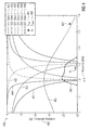
- FIG. 4 shows a graph 400 of exemplary scattering parameters 420 as a function of frequency 410 .
- the scattering parameters 420 are given in dB, while the frequency 410 is given in GHz.
- a range of the scattering parameters 420 on the ordinate scales from 0 to ⁇ 25 dB, while a range of the frequency 410 on the abscissa scales from 1 to 1.6 GHz.
- the exemplary scattering parameters 420 of the graph 400 shown in FIG. 4 may be obtained from the antenna system 300 shown in FIGS. 3 a and 3 b .
- the exemplary scattering parameters 420 can be used to describe the antenna system 300 of FIGS.
- the curve 401 corresponds to the S-parameter S 11 in the first tuner state
- the curve 402 corresponds to the S-parameter S 22 in the first tuner state
- the curve 403 corresponds to the S-parameter S 21 in the first tuner state
- the curve 404 corresponds to the S-parameter S 11 in the second tuner state
- the curve 405 corresponds to the S-parameter S 22 in the second tuner state
- the curve 406 corresponds to the S-parameter S 21 in the second tuner state.
- the point 407 corresponds to the resonant frequency in the first tuner state
- the point 408 corresponds to the resonant frequency in the second tuner state.
- the scattering parameters or S-parameters describe the reflection properties of the antenna system.
- the S-parameter S 11 describes a reflection at the input port of the antenna system (e.g. at the planar inverted F-shaped antenna element 242 )
- the S-parameter S 22 describes a reflection at the output port of the antenna system (e.g. at the planar inverted F-shaped antenna element 244 )
- the S-parameter S 21 describes a forward gain between the input port and the output port (e.g., from the planar inverted F-shaped antenna element 242 to the planar inverted F-shaped antenna element 244 ). It can be seen from the graph 400 of FIG.
- the frequency bandwidth corresponding to the S-parameter S 11 , 401 , 404 essentially decreases
- the frequency bandwidth corresponding to the S-parameter S 22 , 402 , 405 essentially decreases
- the frequency bandwidth corresponding to the S-parameter S 21 , 403 , 406 decreases as well.
- the resonant frequency of the ground plane when switching from the first tuner state to the second tuner state, the resonant frequency of the ground plane will essentially be reduced.
- the resonant frequency 407 of the ground plane in the first tuner state is approximately 1.55 GHz
- the resonant frequency 408 of the ground plane in the second tuner state is approximately 1.25 GHz. Therefore, by switching between the first tuner state and the second tuner state, the resonant frequency of the ground plane can significantly be reduced.
- the tuner can be a variable capacitor or a switch, achieving the desired effect of chassis length modulation through its control signals.
- Two possible uses can be considered for the same tunable chassis mode operation.
- a first case considers the situation where the ground plane size is such that its natural resonance is higher than the one to be used as central frequency for a given standard. For example, if the chassis is 40 ⁇ 100 mm, it will have a natural resonance around 1.2 GHz, while the GSM 900 frequency bandwidth will be needed to be supported.
- the bandwidth can be increased without enlarging the antenna of the chassis, at the expense of a decrease in the isolation level.
- a second case considers that the mutual coupling can be decreased without modifying the antenna, at the expense of a narrower bandwidth.
- the first case was given, as the second case is a dual configuration.
- the two states of the tuner were described in one example.
- the first state essentially corresponds to the situation where the tuner is in the normal default state, not exhibiting any effect on the chassis, meaning the chassis effective length is unchanged. It can be seen like a short circuit that is connecting the two sides of the chassis, deselecting de facto the slot action.
- the second state essentially corresponds to the situation where the tuner is creating a barrier (open circuit) between the two sides of the slot, enabling the current to follow a longer path and thus tuning the electrical length of the chassis.
- the impact of the two states on the scattering parameters of the antenna system shown in FIGS. 3 a and 3 b were described with reference to FIG. 4 according to one example.
- FIGS. 5 a to 5 c show different exemplary implementations 510 , 520 , 530 of one or more switches 515 , 525 , 535 which may be implemented in the antenna system 100 shown in FIG. 1 b .
- the tuner 130 comprises a switch 515 , 525 connected between two opposing sides 511 , 513 of the slot 111 , wherein the switch 515 , 525 is configured to provide a first tuner state by shortening the two opposing sides 511 , 513 of the slot 111 and a second tuner state by disconnecting the two opposing sides 511 , 513 of the slot 111 .
- the switch 515 is connected between end points 517 , 519 of the two opposing sides 511 , 513 of the slot 111 , wherein the end points 517 , 519 are located at an edge 102 of the ground plane 110 .
- the switch 525 is connected between midpoints 527 , 529 of the two opposing sides 511 , 513 of the slot 111 .
- the current flow 101 through the ground plane 110 from the first portion 112 to the second portion 114 is depicted for different examples.
- the first tuner state is provided by the switch 515 , 525
- the current flow 101 can essentially traverse the slot 111 as indicated by the dotted lines in FIGS. 5 a and 5 b .
- the second tuner state is provided by the switch 515 , 525
- the current flow 101 will substantially pass around the slot 111 as indicated by the solid lines shown in FIGS. 5 a and 5 b .
- the influence of the slot to the current flow can essentially be different.
- the length of the current path covered by the current flow in the first tuner state and the second tuner state in the implementation 510 may differ by approximately twice the length of one of the two opposing sides of the slot.
- the length of the current path covered by the current flow in the first tuner state and the second tuner state in the implementation 520 may differ by approximately twice the half of the length of one of the two opposing sides of the slot.
- the tuner 130 comprises a plurality of switches 535 connected between two opposing sides 511 , 513 of the slot 111 , wherein each of the plurality of switches 535 is configured to switch between a closed state and an open state.
- the plurality of switches 535 as shown in the implementation 530 , the influence of the slot 111 to the current flow through the ground plane 110 from the first portion 112 to the second portion 114 can be changed in a more flexible way when compared to the implementations 510 , 520 .
- the provision of the plurality of switches 535 according to the implementation 530 is associated with a higher complexity of the antenna system.
- FIG. 6 shows an example implementation of a switch 600 which may be implemented in the different implementation examples 510 , 520 , 530 shown in FIGS. 5 a to 5 c .
- the switch 600 shown in FIG. 6 may correspond to the one or more switches 515 , 525 , 535 shown in FIGS. 5 a to 5 c .
- the switch 600 comprises a first terminal 601 and a second terminal 602 . These two terminals 601 , 602 can be connected to the two opposing sides 511 , 513 of the slot 111 according to the implementations 510 , 520 , 530 .
- the switch 600 of FIG. 6 is configured to switch between a closed state (I) and an open state (II).
- the switch 600 shown in FIG. 6 may be a mechanical switch or a microelectromechanical systems (MEMS) switch.
- MEMS microelectromechanical systems
- the MEMS switch may comprise a substrate for traversing the slot of the ground plane, two contact elements for electrically connecting the ground plane on two opposing sides with respect to the slot and a capacitive switching element arranged on the substrate for providing the first state (closed state) and the second state (open state).
- the capacitive switching element of the MEMS switch may comprise a movable electrode which can be controlled by a control signal (e.g., a voltage signal) such that the two contact elements on the two opposing sides with respect to the slot will be connected via the movable electrode in the first state and disconnected in the second state.
- FIG. 7 shows a schematic diagram of an exemplary antenna system 700 comprising a variable capacitor (or variable impedance) 705 as a tuner 130 .
- the antenna system 700 shown in FIG. 7 differs from the antenna system 100 shown in FIG. 1 b in that the tuner 130 comprises a variable capacitor or variable impedance 705 connected between two opposing sides 511 , 513 of the slot 111 , wherein the variable capacitor or variable impedance 705 is configured to continuously change a capacitance or impedance thereof.
- the capacitance or impedance of the variable capacitor or variable impedance 705 it is possible to dynamically change the influence of the slot 111 to the current flow through the ground plane 110 from the first portion 112 to the second portion 114 .
- the dynamic change of the influence of the slot to the current flow has the consequence that key parameters such as the impedance bandwidth of the antenna system can continuously be changed. This also provides the tunability of the ground plane mode or chassis mode of the antenna system for use in practical applications.
- FIG. 8 shows a schematic diagram of an example mobile communication device 800 comprising a chassis 810 .
- the mobile communication device 800 shown in FIG. 8 may comprise one of the antenna systems described herein.
- the antenna system of the mobile communication device 800 comprises the first antenna element 122 and the second antenna element 124 .
- the chassis 810 may be formed by at least a part of a PCB (printed circuit board) of the mobile communication device 800 .
- the chassis 810 may be formed by at least a part of a housing (e.g. the outer metallic part) of the mobile communication device 800 .
- the chassis 810 may be a metallic part which acts as a ground for the mobile communication device 800 .
- the antenna system may comprise the following features.
- the antenna system comprises a ground plane 110 , a first antenna element 122 , a second antenna element 124 and a tuner 130 .
- the ground plane 110 comprises at least one slot 111 .
- the first antenna element 122 is coupled to a first portion 112 of the ground plane 110 .
- the second antenna element 124 is coupled to a second portion 114 of the ground plane 110 which is spaced apart from the first portion 112 .
- the tuner 130 is configured to change the influence of the slot 111 to a current flow 101 through the ground plane 110 from the first portion 112 to the second portion 114 .
- the slot 111 comprises two opposing sides 511 , 513 extending in parallel to each other, wherein the two opposing sides 511 , 513 are arranged substantially perpendicular to a connecting line between the first portion 112 and the second portion 114 .
- the tuner 130 comprises a switch 515 or a variable impedance connected between end points 517 , 519 of the two opposing sides 511 , 513 of the slot 111 , wherein the end points 517 , 519 are located at an edge 102 of the ground plane 110 .
- the tuner 130 may be configured to change an impedance of the slot 111 to change a length of a current path covered by the current flow 101 .
- aspects have been described in the context of an apparatus, it is clear that these aspects also represent a description of the corresponding method, where a block or device corresponds to a method step or a feature of a method step. Analogously, aspects described in the context of a method step also represent a description of a corresponding block or item or feature of a corresponding apparatus.
- Some or all of the method steps may be executed by (or using) a hardware apparatus, like for example, a microprocessor, a programmable computer or an electronic circuit. In some examples, some one or more of the most important method steps may be executed by such an apparatus.
- the present antenna system uses a ground plane having a slot (or a segmented ground plane) that allows the tunability of the chassis mode. It allows to electrically enlarge the chassis dimensions and to control the level of isolation without having effects on the handset total dimensions.
- the present antenna system uses a small antenna with the advantages it has for the industrial design.
- the ground plane having the slot or the segmented ground plane it is possible to achieve tunability of the chassis mode and control the impedance bandwidth and the isolation adaptively.
- the better performance of the presented antenna system can be obtained by focusing on tuning of the chassis mode, taking advantage of the aforementioned coupling phenomena. This can essentially be achieved by varying the electrical length of the chassis depending on the needs.
Abstract
Description
Claims (22)
Priority Applications (4)
| Application Number | Priority Date | Filing Date | Title |
|---|---|---|---|
| US13/570,327 US8884835B2 (en) | 2012-08-09 | 2012-08-09 | Antenna system, method and mobile communication device |
| DE102013108132.0A DE102013108132A1 (en) | 2012-08-09 | 2013-07-30 | Antenna system, method and mobile communication device |
| CN201310341199.XA CN103579778A (en) | 2012-08-09 | 2013-08-07 | Antenna system, method and mobile communication device |
| CN201811105678.0A CN109193153B (en) | 2012-08-09 | 2013-08-07 | Antenna system, method and mobile communication device |
Applications Claiming Priority (1)
| Application Number | Priority Date | Filing Date | Title |
|---|---|---|---|
| US13/570,327 US8884835B2 (en) | 2012-08-09 | 2012-08-09 | Antenna system, method and mobile communication device |
Publications (2)
| Publication Number | Publication Date |
|---|---|
| US20140043201A1 US20140043201A1 (en) | 2014-02-13 |
| US8884835B2 true US8884835B2 (en) | 2014-11-11 |
Family
ID=49999304
Family Applications (1)
| Application Number | Title | Priority Date | Filing Date |
|---|---|---|---|
| US13/570,327 Active 2033-02-27 US8884835B2 (en) | 2012-08-09 | 2012-08-09 | Antenna system, method and mobile communication device |
Country Status (3)
| Country | Link |
|---|---|
| US (1) | US8884835B2 (en) |
| CN (2) | CN109193153B (en) |
| DE (1) | DE102013108132A1 (en) |
Cited By (7)
| Publication number | Priority date | Publication date | Assignee | Title |
|---|---|---|---|---|
| US20130234901A1 (en) * | 2012-03-08 | 2013-09-12 | Acer Incorporated | Tunable Slot Antenna |
| US20140049432A1 (en) * | 2007-06-21 | 2014-02-20 | Apple Inc. | Antennas for handheld electronic devices |
| US9502773B2 (en) * | 2015-03-24 | 2016-11-22 | Htc Corporation | Mobile device and manufacturing method thereof |
| US20180083367A1 (en) * | 2016-09-22 | 2018-03-22 | Qualcomm Incorporated | Common-ground-plane antennas |
| US10910715B2 (en) * | 2017-02-27 | 2021-02-02 | Proant Ab | Antenna arrangement and a device comprising such an antenna arrangement |
| WO2021171650A1 (en) * | 2020-02-27 | 2021-09-02 | パナソニックIpマネジメント株式会社 | Antenna device |
| WO2023067196A1 (en) | 2021-10-22 | 2023-04-27 | Ignion, S.L. | SELF-TUNABLE IoT DEVICE AND RADIATING SYSTEM BASED ON NON-RESONANT RADIATION ELEMENTS |
Families Citing this family (20)
| Publication number | Priority date | Publication date | Assignee | Title |
|---|---|---|---|---|
| US10014568B2 (en) * | 2014-12-18 | 2018-07-03 | Sony Corporation | Mobile communication device |
| CN106415926B (en) * | 2014-12-30 | 2021-01-05 | 华为技术有限公司 | Antenna device and terminal |
| TWI553959B (en) * | 2015-01-23 | 2016-10-11 | 泓博無線通訊技術有限公司 | Slot antenna with multiple boundary conditions |
| KR20160099359A (en) * | 2015-02-12 | 2016-08-22 | 삼성전기주식회사 | In-mold antenna, apparatus for controlling antenna characteristic and method for manufacturing in-mold antenna |
| US9537210B2 (en) * | 2015-03-25 | 2017-01-03 | Intel IP Corporation | Antenna card for controlling and tuning antenna isolation to support carrier aggregation |
| CN106486765A (en) * | 2015-08-25 | 2017-03-08 | 中兴通讯股份有限公司 | A kind of antenna assembly reducing multi-input multi-output system Antenna Correlation and terminal |
| EP3163676B1 (en) * | 2015-10-29 | 2019-04-24 | Thomson Licensing | Circuit board for an antenna assembly |
| US10431891B2 (en) | 2015-12-24 | 2019-10-01 | Intel IP Corporation | Antenna arrangement |
| CN105529535A (en) * | 2016-01-15 | 2016-04-27 | 昆山联滔电子有限公司 | Composite antenna |
| WO2017181376A1 (en) * | 2016-04-20 | 2017-10-26 | 华为技术有限公司 | Slot antenna and terminal device |
| EP3244486A1 (en) * | 2016-05-09 | 2017-11-15 | Thomson Licensing | Antenna device for the coexistence of wireless systems |
| KR20230051313A (en) | 2017-03-06 | 2023-04-17 | 스냅 인코포레이티드 | Wearable device antenna system |
| JP2018170589A (en) * | 2017-03-29 | 2018-11-01 | 富士通株式会社 | Antenna device, and electronic equipment |
| US10615486B2 (en) * | 2017-06-28 | 2020-04-07 | Intel IP Corporation | Antenna system |
| CN108288763A (en) * | 2018-01-03 | 2018-07-17 | 上海传英信息技术有限公司 | Mobile terminal and its antenna installation method |
| CN108832313B (en) * | 2018-05-28 | 2021-03-02 | Oppo广东移动通信有限公司 | Electronic device |
| CN112805878B (en) * | 2018-10-10 | 2022-05-24 | 华为技术有限公司 | Antenna, wireless device and antenna array |
| CN109841944B (en) * | 2019-03-26 | 2021-07-27 | 青岛海信移动通信技术股份有限公司 | Antenna and terminal |
| CN110752445B (en) * | 2019-10-25 | 2021-10-15 | 歌尔科技有限公司 | Antenna radiation system and communication terminal |
| CN113270728B (en) * | 2021-04-26 | 2022-07-12 | 宁波大学 | Tunable decoupling network for multi-antenna system |
Citations (7)
| Publication number | Priority date | Publication date | Assignee | Title |
|---|---|---|---|---|
| US6624789B1 (en) * | 2002-04-11 | 2003-09-23 | Nokia Corporation | Method and system for improving isolation in radio-frequency antennas |
| US6864848B2 (en) * | 2001-12-27 | 2005-03-08 | Hrl Laboratories, Llc | RF MEMs-tuned slot antenna and a method of making same |
| US6917337B2 (en) * | 2002-06-05 | 2005-07-12 | Fujitsu Limited | Adaptive antenna unit for mobile terminal |
| DE202007019033U1 (en) | 2007-04-10 | 2010-04-22 | Nokia Corp. | Antenna arrangement and device with an antenna arrangement |
| US8552913B2 (en) * | 2009-03-17 | 2013-10-08 | Blackberry Limited | High isolation multiple port antenna array handheld mobile communication devices |
| US20130300625A1 (en) * | 2012-05-11 | 2013-11-14 | Acer Incorporated | Communication device and mimo (multi-input multi-output) antenna system therein |
| US8643558B2 (en) * | 2010-04-28 | 2014-02-04 | Hon Hai Precision Industry Co., Ltd. | Multi-frequency antenna |
Family Cites Families (9)
| Publication number | Priority date | Publication date | Assignee | Title |
|---|---|---|---|---|
| JPH0229007A (en) * | 1988-07-18 | 1990-01-31 | Mitsubishi Electric Corp | Antenna system |
| GB0102768D0 (en) * | 2001-02-02 | 2001-03-21 | Koninkl Philips Electronics Nv | Wireless terminal |
| FI115343B (en) * | 2001-10-22 | 2005-04-15 | Filtronic Lk Oy | Internal multi-band antenna |
| SE528088C2 (en) * | 2004-09-13 | 2006-08-29 | Amc Centurion Ab | Antenna device and portable radio communication device including such antenna device |
| EP1858112B1 (en) * | 2006-05-19 | 2010-07-07 | AMC Centurion AB | Metal housing with slot antenna for a radio communication device |
| US7612725B2 (en) * | 2007-06-21 | 2009-11-03 | Apple Inc. | Antennas for handheld electronic devices with conductive bezels |
| CN201345425Y (en) * | 2008-09-27 | 2009-11-11 | 耀登科技股份有限公司 | Double-frequency space diversity double antenna for movable termination |
| US9070969B2 (en) * | 2010-07-06 | 2015-06-30 | Apple Inc. | Tunable antenna systems |
| CN102368575A (en) * | 2011-09-08 | 2012-03-07 | 广东欧珀移动通信有限公司 | Built-in secondary radiating antenna |
-
2012
- 2012-08-09 US US13/570,327 patent/US8884835B2/en active Active
-
2013
- 2013-07-30 DE DE102013108132.0A patent/DE102013108132A1/en active Pending
- 2013-08-07 CN CN201811105678.0A patent/CN109193153B/en active Active
- 2013-08-07 CN CN201310341199.XA patent/CN103579778A/en active Pending
Patent Citations (7)
| Publication number | Priority date | Publication date | Assignee | Title |
|---|---|---|---|---|
| US6864848B2 (en) * | 2001-12-27 | 2005-03-08 | Hrl Laboratories, Llc | RF MEMs-tuned slot antenna and a method of making same |
| US6624789B1 (en) * | 2002-04-11 | 2003-09-23 | Nokia Corporation | Method and system for improving isolation in radio-frequency antennas |
| US6917337B2 (en) * | 2002-06-05 | 2005-07-12 | Fujitsu Limited | Adaptive antenna unit for mobile terminal |
| DE202007019033U1 (en) | 2007-04-10 | 2010-04-22 | Nokia Corp. | Antenna arrangement and device with an antenna arrangement |
| US8552913B2 (en) * | 2009-03-17 | 2013-10-08 | Blackberry Limited | High isolation multiple port antenna array handheld mobile communication devices |
| US8643558B2 (en) * | 2010-04-28 | 2014-02-04 | Hon Hai Precision Industry Co., Ltd. | Multi-frequency antenna |
| US20130300625A1 (en) * | 2012-05-11 | 2013-11-14 | Acer Incorporated | Communication device and mimo (multi-input multi-output) antenna system therein |
Non-Patent Citations (3)
| Title |
|---|
| Aberle, et al. "Reconfigurable Antennas for Portable Wireless Devices" IEEE Antennas and Propagation Magazine, vol. 45, No. 6, Dec. 2003. 7 Pages. |
| Jose, et al. "Experimental Investigations on Electronically Tunable Microstrip Antennas" Microwave and Optical Technology Letters, vol. 20, No. 3, Feb. 5, 1999. 4 Pages. |
| Vainikainen, et al. "Resonator-Based Analysis of the Combination of Mobile Handset Antenna and Chassis" IEEE Transactions on Antennas and Propagation, vol. 50, No. 10, Oct. 2002. 12 Pages. |
Cited By (13)
| Publication number | Priority date | Publication date | Assignee | Title |
|---|---|---|---|---|
| US20140049432A1 (en) * | 2007-06-21 | 2014-02-20 | Apple Inc. | Antennas for handheld electronic devices |
| US9356355B2 (en) * | 2007-06-21 | 2016-05-31 | Apple Inc. | Antennas for handheld electronic devices |
| US9882269B2 (en) | 2007-06-21 | 2018-01-30 | Apple Inc. | Antennas for handheld electronic devices |
| US9356356B2 (en) * | 2012-03-08 | 2016-05-31 | Acer Incorporated | Tunable slot antenna |
| US20130234901A1 (en) * | 2012-03-08 | 2013-09-12 | Acer Incorporated | Tunable Slot Antenna |
| US10044096B2 (en) | 2015-03-24 | 2018-08-07 | Htc Corporation | Mobile device and manufacturing method thereof |
| US9502773B2 (en) * | 2015-03-24 | 2016-11-22 | Htc Corporation | Mobile device and manufacturing method thereof |
| US20180083367A1 (en) * | 2016-09-22 | 2018-03-22 | Qualcomm Incorporated | Common-ground-plane antennas |
| US10910715B2 (en) * | 2017-02-27 | 2021-02-02 | Proant Ab | Antenna arrangement and a device comprising such an antenna arrangement |
| WO2021171650A1 (en) * | 2020-02-27 | 2021-09-02 | パナソニックIpマネジメント株式会社 | Antenna device |
| JPWO2021171650A1 (en) * | 2020-02-27 | 2021-09-02 | ||
| JP7054858B2 (en) | 2020-02-27 | 2022-04-15 | パナソニックIpマネジメント株式会社 | Antenna device |
| WO2023067196A1 (en) | 2021-10-22 | 2023-04-27 | Ignion, S.L. | SELF-TUNABLE IoT DEVICE AND RADIATING SYSTEM BASED ON NON-RESONANT RADIATION ELEMENTS |
Also Published As
| Publication number | Publication date |
|---|---|
| US20140043201A1 (en) | 2014-02-13 |
| CN109193153B (en) | 2024-03-26 |
| CN103579778A (en) | 2014-02-12 |
| DE102013108132A1 (en) | 2014-02-13 |
| CN109193153A (en) | 2019-01-11 |
Similar Documents
| Publication | Publication Date | Title |
|---|---|---|
| US8884835B2 (en) | Antenna system, method and mobile communication device | |
| KR100906510B1 (en) | Antenna arrangement | |
| KR100993439B1 (en) | Antenna arrangement | |
| JP4707495B2 (en) | Antenna device and radio device | |
| US8638266B2 (en) | Antenna arrangement and a radio apparatus including the antenna arrangement | |
| TWI637561B (en) | Mobile device | |
| US6963308B2 (en) | Multiband antenna | |
| JP5009240B2 (en) | Multiband antenna and wireless communication terminal | |
| JP6490080B2 (en) | Technology to adjust antenna by weak coupling of variable impedance element | |
| US20040227678A1 (en) | Compact tunable antenna | |
| EP1052722A2 (en) | Antenna | |
| WO2007112184A2 (en) | Communications assembly and antenna assembly with a switched tuning line | |
| CN110556619B (en) | Antenna structure and wireless communication device with same | |
| TWI539676B (en) | Communication device | |
| US8207895B2 (en) | Shorted monopole antenna | |
| WO2008010149A1 (en) | Antenna with reduced sensitivity to user finger position | |
| CN110770975B (en) | Antenna arrangement and device comprising such an antenna arrangement | |
| KR100695813B1 (en) | Multiplex band internal antenna using a band reject filter and impedance matching circuit | |
| JPH09232854A (en) | Small planar antenna system for mobile radio equipment | |
| EP2775562B1 (en) | Communication device and antenna element therein | |
| KR20020087139A (en) | Wireless terminal | |
| EP2173006A1 (en) | Multi-band antenna device and portable radio communication device comprising such an antenna device | |
| Desjardins | Reconfigurable Dielectric Resonator Antennas | |
| Kingsley et al. | In search of the perfect handset antenna |
Legal Events
| Date | Code | Title | Description |
|---|---|---|---|
| AS | Assignment |
Owner name: INTEL MOBILE COMMUNICATIONS GMBH, GERMANY Free format text: ASSIGNMENT OF ASSIGNORS INTEREST;ASSIGNORS:PELOSI, MAURO;TATOMIRESCU, ALEXANDRU DANIEL;KNUDSEN, MIKAEL BERGHOLZ;AND OTHERS;SIGNING DATES FROM 20120813 TO 20120828;REEL/FRAME:029097/0466 |
|
| FEPP | Fee payment procedure |
Free format text: PAYOR NUMBER ASSIGNED (ORIGINAL EVENT CODE: ASPN); ENTITY STATUS OF PATENT OWNER: LARGE ENTITY |
|
| STCF | Information on status: patent grant |
Free format text: PATENTED CASE |
|
| AS | Assignment |
Owner name: INTEL DEUTSCHLAND GMBH, GERMANY Free format text: CHANGE OF NAME;ASSIGNOR:INTEL MOBILE COMMUNICATIONS GMBH;REEL/FRAME:037057/0061 Effective date: 20150507 |
|
| MAFP | Maintenance fee payment |
Free format text: PAYMENT OF MAINTENANCE FEE, 4TH YEAR, LARGE ENTITY (ORIGINAL EVENT CODE: M1551) Year of fee payment: 4 |
|
| AS | Assignment |
Owner name: INTEL CORPORATION, CALIFORNIA Free format text: CONFIRMATORY ASSIGNMENT EFFECTIVE AS OF JANUARY 1, 2018;ASSIGNOR:INTEL DEUTSCHLAND GMBH;REEL/FRAME:053477/0121 Effective date: 20200615 |
|
| AS | Assignment |
Owner name: APPLE INC., CALIFORNIA Free format text: ASSIGNMENT OF ASSIGNORS INTEREST;ASSIGNOR:INTEL CORPORATION;REEL/FRAME:053518/0765 Effective date: 20191130 |
|
| MAFP | Maintenance fee payment |
Free format text: PAYMENT OF MAINTENANCE FEE, 8TH YEAR, LARGE ENTITY (ORIGINAL EVENT CODE: M1552); ENTITY STATUS OF PATENT OWNER: LARGE ENTITY Year of fee payment: 8 |