US8804792B1 - Intermediary signal conditioning device with interruptible detection mode - Google Patents
Intermediary signal conditioning device with interruptible detection mode Download PDFInfo
- Publication number
- US8804792B1 US8804792B1 US13/766,647 US201313766647A US8804792B1 US 8804792 B1 US8804792 B1 US 8804792B1 US 201313766647 A US201313766647 A US 201313766647A US 8804792 B1 US8804792 B1 US 8804792B1
- Authority
- US
- United States
- Prior art keywords
- signal
- conditioning device
- input
- detection mode
- output
- Prior art date
- Legal status (The legal status is an assumption and is not a legal conclusion. Google has not performed a legal analysis and makes no representation as to the accuracy of the status listed.)
- Active
Links
Images


Classifications
-
- H—ELECTRICITY
- H04—ELECTRIC COMMUNICATION TECHNIQUE
- H04L—TRANSMISSION OF DIGITAL INFORMATION, e.g. TELEGRAPHIC COMMUNICATION
- H04L25/00—Baseband systems
- H04L25/02—Details ; arrangements for supplying electrical power along data transmission lines
- H04L25/20—Repeater circuits; Relay circuits
-
- H—ELECTRICITY
- H04—ELECTRIC COMMUNICATION TECHNIQUE
- H04L—TRANSMISSION OF DIGITAL INFORMATION, e.g. TELEGRAPHIC COMMUNICATION
- H04L25/00—Baseband systems
- H04L25/02—Details ; arrangements for supplying electrical power along data transmission lines
- H04L25/03—Shaping networks in transmitter or receiver, e.g. adaptive shaping networks
- H04L25/03878—Line equalisers; line build-out devices
- H04L25/03885—Line equalisers; line build-out devices adaptive
Definitions
- One or more embodiments generally relate to integrated circuit devices (“ICs”). More particularly, one or more embodiments relate generally to an intermediary signal conditioning device or a signal integrity device.
- ICs integrated circuit devices
- High-speed serial data driven between a transmitter and a receiver can deteriorate or suffer signal losses over distance or time. Such losses or deterioration may be conditioned by an intermediary signal conditioning device or a signal integrity device.
- intermediary signal conditioning devices or signal integrity devices are sometimes called repeaters, buffers, re-drivers, and other names.
- One or more aspects generally relate to an intermediary signal conditioning device with an input adaptive detection mode.
- an embodiment relates generally to an apparatus.
- an intermediary signal conditioning device has a control module, an input module, and an output module.
- the input module and the control module are for receiving an input signal.
- the control module is configured to interrupt the output module within a duration of time to allow at least a minimum pulse length of the input signal to be output as an output signal from the output module.
- the intermediary signal conditioning device is configured to condition the input signal for retransmission as the output signal.
- an intermediary signal conditioning device has a control module, an input module, and an output module.
- the input module and the control module are for receiving an input signal.
- the control module is configured to interrupt a detection mode of the intermediary signal conditioning device within a duration of time to allow at least a minimum pulse length of the input signal to be output as an output signal from the output module.
- the intermediary signal conditioning device is configured to condition the input signal for retransmission as the output signal.
- an intermediary signal conditioning device is operated in a detection mode.
- a transmitted signal is received to an input module and a control module of the intermediary signal conditioning device while in the detection mode.
- the intermediary signal conditioning device responds to receipt of the transmitted signal by switching from the detection mode to a retransmission mode within a duration of time sufficient to allow at least a minimum pulse length of the transmitted signal to be processed as an input signal for retransmission as an output signal.
- the input signal is conditioned by the intermediary signal conditioning device for retransmission.
- the input signal is retransmitted as an output signal via an output module of the intermediary signal conditioning device.
- FIG. 1 is a block/circuit diagram depicting an exemplary embodiment of an intermediary signal conditioning device with an input adaptive detection mode.
- FIG. 2 is a block/circuit diagram depicting an exemplary embodiment of a re-driver conditioning device with an interruptible detection mode.
- FIG. 3 is a flow diagram depicting an exemplary embodiment of an interruptible receiver detection mode process.
- FIG. 4 is a flow diagram depicting an exemplary embodiment of a state machine.
- FIG. 5 is a flow diagram depicting an exemplary embodiment of the state machine of FIG. 4 for an IC chip embodiment of the re-driver conditioning device of FIG. 2 .
- FIG. 6 is a perspective view depicting an exemplary embodiment of a system having an adapter with the re-driver conditioning device of FIG. 2 .
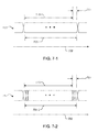
- FIGS. 7-1 and 7 - 2 are respective signal diagrams depicting respective exemplary embodiments of a transmitted or input (“input”) signal having a pulse width or pulse length or envelope length.
- a transmitter such as a host computer device (“host”) for example, sends a signal to an intermediary signal conditioning device while such intermediary signal conditioning device is in a receiver detection mode.
- a signal may have a pulse length that is effectively too short to be retransmitted while the intermediary signal conditioning device is in a receiver detection mode, namely too short to survive completion of a receiver detection mode or too much signal would be lost by waiting for completion of a receiver detection mode.
- an intermediary signal conditioning device While in a receiver detection mode, which prevented transmission by a host.
- such intermediary signal conditioning device would effectively block or not do anything with a host transmitted signal effectively preventing communication with a receiver.
- a host encountering such an unresponsive intermediary signal conditioning device, may determine that a communication link (“link”) between the host and the receiver is broken, and accordingly such host may attempt to reset the link, which may include the host sending a training signal, initiating a receiver detection mode of the host, or other protocol activities for resetting the link or “handshake.”
- FIG. 1 is a block/circuit diagram depicting an exemplary embodiment of a signal integrity or an intermediary signal conditioning device (“intermediary signal conditioning device”) 100 with an input adaptable detection mode.
- Intermediary signal conditioning device 100 has a control module 192 , an input module 193 , and an output module 194 .
- Intermediary signal conditioning device 100 may be a re-driver or a re-timer. For purposes of clarity by way of example and not limitation, it shall be assumed that intermediary signal conditioning device 100 is a re-driver.
- Input module 193 and control module 192 are coupled to receive an input signal via a transmitter-side input module or interface (“input interface”) 101 .
- input signal is a differential signal having a plus port 190 and a minus port 191 .
- input interface 101 is a differential current mode logic (“CML”) input.
- Control module 192 may include a differential amplifier 151
- input module 193 may include a differential amplifier 152
- Input module 193 may optionally include a filter block, such as equalizer 154 for example.
- Differential amplifier 151 may have an input port coupled to plus port 190 and another input port coupled to minus port 191 .
- differential amplifier 152 may have an input port coupled to plus port 190 and another input port coupled to minus port 191 .
- Output of differential amplifier 152 may be provided to equalizer 154
- output of equalizer 154 may be provided to a signal boosting block, such as limiting amplifier 156 for example.
- Output module 194 may include a differential driver 160 .
- output module 194 may include a limiting amplifier 156 .
- Output of limiting amplifier 156 may be provided as an input to differential driver 160 .
- Output of differential driver 160 may be provided as an output signal via a receiver-side output module or interface (“output interface”) 102 .
- Differential driver 160 includes a detection port 183 .
- Output of differential amplifier 151 may be provided as a control signal 182 to detection port 183 to differential driver 160 .
- differential amplifier 151 may act as a signal detector.
- Control signal 182 may be used to indicate when an input signal is received by input interface 101 .
- Output module 194 may be configured to provide a control signal 181 to control module 192 .
- Control signal 181 may be used to indicate when output module 194 is in a detection mode or a retransmission mode.
- intermediary signal conditioning device 100 may condition an input signal received via input interface 101 for retransmission as output signal via output interface 102 .
- intermediary signal conditioning device 100 may be in a detection mode, where such detection mode is an input adaptable detection mode as described below in further detail.
- control module 192 may be configured to interrupt output module 194 and transition from a detection mode to a retransmission mode within a short amount of time. Such short amount of time may be associated with a predetermined length of an input signal to allow loss of a portion of such input signal while still allowing a threshold amount of the remainder of such input signal to be output as an output signal from output module 194 .
- interruption of a detection mode it is generally meant that a detection mode may be suspended, halted, exited, put on hold, adjusted, or otherwise affected. Such interruption is used to allow intermediary signal conditioning device 100 to transition out of a detection mode to have an input signal, such as a transmitted signal, be retransmitted as an output signal, as described below in additional detail.
- a detection mode may be for the purpose of detecting the presence or absence of a receiver, a load, or any other electrical component coupled to output interface 102 .
- a specification may effectively state that at least 90 percent of an input signal must be made available, or, stated in other terms, at most 10 percent of an input signal state may be lost and still meet the specification threshold.
- a specification threshold level may be used.
- a predetermined signal length of an input signal may relate to a signal transmission or retransmission parameter of a specification.
- Such a specification may be related to a protocol. Examples of such protocols may include without limitation USB, PCIe, SAS, and SATA.
- a predetermined signal length of an input signal which may be lost may be associated with or within a duration of time for intermediary signal conditioning device 100 to go from a detection mode to a retransmission mode to output such input signal as an output signal.
- a minimum pulse width that may be passed as an output may be associated with such duration of time in which a portion of such pulse width may be lost.
- Such duration of time may be substantially less than a minimum pulse length of an input signal.
- duration of time may be less than approximately 10 percent of a minimum pulse length of an input signal.
- at least 90 percent of an input pulse length of an input signal may be provided for output as output signal.
- an interrupt time of intermediary signal conditioning device 100 for going from a detection mode to a retransmission mode may be equal to or less than an allowable amount of loss of an output length of an input signal.
- Control module 192 may be configured to interrupt output module 194 to allow a substantial portion of an input signal received during a detection mode to be retransmitted by intermediary signal conditioning device 100 as an output signal. For example, in response to receiving an input signal at input interface 101 , control module 192 may be cause suspension or exiting of a detection mode by output module 194 .
- a detection mode may be a receiver detection mode or a load detection mode.
- FIG. 2 is a block/circuit diagram depicting an exemplary embodiment of a re-driver conditioning device 200 with an interruptible detection mode.
- Re-driver conditioning device may be an embodiment of intermediary signal conditioning device 100 of FIG. 1 .
- intermediary signal conditioning device 100 of FIG. 1 As some description of re-driver conditioning device 200 is the same as corresponding description of intermediary signal conditioning device 100 of FIG. 1 , such same description is not repeated for clarity.
- Re-driver conditioning device 200 includes input interface 101 , differential amplifiers 151 and 152 , equalizer 154 , adder 155 , DC offset canceller 153 , limiting amplifier 156 , de-emphasis controller 168 , swing controller 170 , delay buffer 157 , buffer 158 , differential driver 160 , receiver detector 159 , resistors 161 , 162 , 164 and 165 , voltage regulator and power manager 130 , slumber mode and receiver detection controller (“control circuit”) 120 , and output interface 102 , as well as switches 186 through 189 .
- switches 186 through 189 may be digital switches implemented with transistors.
- re-driver conditioning device 200 When re-driver conditioning device 200 is ready to receive transmitted signals from a transmitter, input interface 101 is in a first state, and when re-driver conditioning device 200 is not ready to receive transmitted signals from a transmitter, input interface 101 is in a second state.
- re-driver conditioning device 200 supports various specifications or protocols in communications, computing, storage and other applications.
- re-driver conditioning device 200 can be used in USB 3.0, SAS, SATA, or PCIe applications, interfaces, systems, or networks; however, re-driver conditioning device 200 may be used in any of a variety of interfaces, applications, systems, or networks, including with any of a variety of specifications in computing, networking, communications, storage, and other areas.
- input interface 101 and output interface 102 may be configured to receive and send, respectively, signals in conformance with any of a variety of protocols and/or specifications.
- input interface 101 of intermediary signal conditioning device 100 may be at 50 ohms, and in a not ready to receive state, input interface 101 of intermediary signal conditioning device 100 may in a high impedance state, namely a “Hi-Z” state.
- an end of each of resistors 161 and 162 may respectively be coupled to a supply voltage via digital switches 186 and 187 , such as Vbias 163 for example, and other ends of resistors 161 and 162 may respectively be coupled to plus and minus ports of input interface 101 .
- a transmitter When in a ready to receive state, a transmitter, such as a USB3 interface of a host for example, may transmit a signal 111 to input interface 101 .
- signal 111 may be intended for conditioning and transmission by re-driver conditioning device 200 to a receiver, such as a USB3 peripheral device (“peripheral”) for example.
- a receiver such as a USB3 peripheral device (“peripheral”) for example.
- signal 111 may have a minimum signal or pulse length, as previously described and described below in additional detail.
- the example of USB3 is described herein for purposes of clarity by way of example and not limitation, as it should be understood that other protocols may be used.
- An example of input single 111 is further described below with reference to FIG. 7 .
- differential amplifier 151 in this embodiment is configured as an input threshold detector.
- differential amplifier 151 is configured to detect when and input signal 111 is present at input interface 101 .
- Differential amplifier 152 in this embodiment is configured as a CML input buffer.
- Output of differential amplifier 152 is provided to equalizer 154 .
- Output of equalizer 154 is provided to adder 155 for subtraction with an output of DC offset canceller 153 .
- Output of adder 155 is provided to limiting amplifier 156 .
- Output of limiting amplifier is provided to DC offset canceller 153 for a previously described feedback input, as well as provided to buffer 158 and delay buffer 157 .
- a de-emphasis control signal 169 may be provided to de-emphasis controller 168
- a swing control signal 170 may be provided to swing controller 167 .
- Outputs of de-emphasis controller 168 and swing controller 167 may be provided as control signal inputs to delay buffer 157 , buffer 158 and differential driver 160 .
- Buffered data from input signal 111 output from either buffer 158 or delay buffer 157 may be input to differential driver 160 for output as an output signal via output interface 102 .
- Differential driver 160 in this exemplary embodiment is a CML output buffer.
- An output of differential driver 160 is coupled to receiver detector 159 .
- Receiver detector 159 may be for checking for a load when re-driver conditioning device 200 is in a load or receiver detection mode.
- Outputs of differential driver 160 are respectively coupled to ends of resistors 164 and 165 , and other ends of resistors 164 and 165 are respectively coupled to Vbias 163 via digital switches 188 and 189 .
- output of differential driver 160 may be coupled for conditional pull-up to provide a low resistance state, such as approximately a 50-ohm impedance for example, or a Hi-Z state.
- Differential driver 160 may be coupled to receive output from differential amplifier 151 as a control signal 182 to terminate a detection mode in response to a threshold amount of input signal detected by differential amplifier 151 .
- Voltage regulator and power manager 130 may be coupled to receive a supply voltage 132 and provide a supply voltage 131 , such as for providing Vbias 163 for example. Voltage regulator and power manager 130 may be activated by assertion of a chip enable (“CE”) signal 133 .
- CE chip enable
- Re-driver conditioning device 200 may include control circuit 120 as part of control module 192 of FIG. 1 .
- Control circuit 120 may include a state machine 121 .
- Control circuit 120 may be configured to put re-driver conditioning device 200 into and out of a detection mode and a slumber mode.
- detection mode may be a receiver detection mode, such as part of “receiver detect control,” or such detection mode may be a load, such as a resistive load, detection mode.
- control circuit 120 may be a slumber mode and receiver detection controller.
- Control circuit may be coupled to receive a compliance test mode signal 134 and to assert or de-assert activation or enable signals 135 for other blocks of re-driver condition device 200 in accordance with the description herein.
- a receiver detection input or pin of control circuit 120 may be pulled high for example to activate an automatic receiver detection mode entry of re-driver conditioning device 200 .
- a receiver detection loop may become active if a corresponding channel's signal detector is idle for longer than a predetermined time. Such channel may move to an unplug mode if no load is detected or may return to a low power mode, namely a slumber mode, due to inactivity.
- re-driver conditioning device 200 may periodically enter into a receiver detection mode via control circuit 120 to determine whether a peripheral is still coupled to receiver-side output interface 102 , namely to determine whether a communication link or handshake with such peripheral is still present based on detection of a load.
- FIG. 3 is a flow diagram depicting an exemplary embodiment of an interruptible receiver detection mode process 300 .
- re-driver conditioning device 200 is operating in a receiver detection mode under control of control circuit 120 .
- a host may go into an idle mode or a power saving mode, during which time such host may not transmit any signal 111 .
- control circuit 120 may cause re-driver conditioning device 200 to go into a receiver detection mode or a load detection mode.
- control circuit 120 may put re-driver conditioning device 100 into a receiver detection mode. If after a receiver detection mode is completed and no load is detected as coupled to receiver-side output interface 102 , then transmitter-side input interface 101 may be put into a Hi-Z state.
- a host may interpret such Hi-Z state as an absence of load on an opposing end of a communication link, namely in this example the peripheral may no longer be attached.
- re-driver conditioning device 200 periodically verifies the continued presence of such peripheral in place of a host. In other words, if a host were directly connected to a peripheral without an intermediary signal conditioning device, then such host would employ a host receiver detection mode.
- re-driver conditioning device 200 may continue to persist in the existence of such communication link or channel by keeping transmitter-side input interface at approximately 50 ohms, namely in a ready to receive state, until no load is detected as a result of completion of a receiver detection mode.
- transmitter-side input interface at approximately 50 ohms, namely in a ready to receive state
- re-driver conditioning device 200 is operating in a receiver detection mode and such mode takes some amount of time, for example approximately 15 microseconds ( ⁇ s), to complete. Further assume that when in such receiver detection mode, at 302 a transmitted signal 111 to transmitter-side input interface 101 of re-driver conditioning device 200 is received. Furthermore, assume that duration of such receiver detection mode, namely completion of a cycle of such a mode, is longer than a predetermined signal length 110 .
- such predetermined signal length 110 may be a minimum pulse length 110 or other minimum or threshold limit for a transmitted signal 111 in accordance with the description herein.
- control circuit 120 may be configured to cause re-driver conditioning device 200 at 303 to interrupt a receiver detection mode, namely interrupt such receiver detection mode.
- control circuit 120 may be configured to cause re-driver conditioning device 200 to exit or suspend a receiver detection mode and enter into a retransmission mode within the duration of a predetermined pulse length 110 of transmitted signal 111 .
- predetermined pulse length 110 may be a minimum pulse length for a network protocol, as previously described. Further, for example, predetermined pulse length 110 may be a minimum pulse length for a network protocol for a transmission parameter, as previously described.
- control circuit 120 may vary from application-to-application. However, for purposes of clarity by way of example and not limitation, it shall be assumed that such transition from receiver detection mode to retransmission mode is on the order of approximately 20 nanosecond (“ns”).
- re-driver conditioning device 200 may be operating in a low power mode to conserve energy.
- control circuit 120 may cause re-driver conditioning device 200 to transition from such low power mode to a normal power mode for retransmission.
- the amount of time to perform such transition may be less than or equal to approximately 20 ns in the example, so, within a sufficiently short time, re-driver conditioning device 200 may be transitioned from a receiver detection mode to a retransmission mode to process a detected input signal from a host.
- transmitted signal 111 may be conditioned by re-driver conditioning device 200 for retransmission.
- transmitted signal 111 may be retransmitted by re-driver conditioning device 200 via receiver-side output interface 102 , as previously described herein.
- 20 ns, 15 ⁇ s, 5 ms, and 50 ohms have been used for purposes of clarity by way of example, it should be understood that these or any other values may be used in accordance with the above description.
- an insignificant amount of transmitted signal 111 may be lost due to transitioning from a detection mode to a retransmission mode, as previously described herein.
- FIG. 4 is a flow diagram depicting an exemplary embodiment of a state machine 121 .
- state machine 121 has four modes, namely a power down mode 402 , an unplugged mode 403 , a slumber mode 404 , and an active (operating) mode 405 .
- State machine 121 may go from power down mode 402 to unplugged mode 403 or to operating mode 405 .
- state machine 121 may go to slumber mode 404 , and from operating mode 405 , state machine may go to slumber mode 404 .
- state machine 121 may go either to unplugged mode 403 or operating mode 405 .
- Unplugged mode 403 does not necessarily mean that a host device or other device used to send a transmission to intermediary signal conditioning device 100 of FIG. 1 is actually unplugged, as such device may be idle for a sufficient time, as previously described, so as to allow intermediary signal conditioning device 100 to enter into a receiver detection mode 410 .
- intermediary signal conditioning device 100 may be in a slumber mode 404 or other low power mode, and thus go into a receiver detection mode 410 .
- FIG. 5 is a flow diagram depicting an exemplary embodiment of state machine 121 of FIG. 4 for an IC chip embodiment of re-driver conditioning device 200 of FIG. 2 .
- Intermediary signal conditioning device 100 may be provided as an IC having a plurality of pinouts or pads.
- One such pad may be for a receive detect activation, namely an _RxDet_EN pad, which may be used to activate a receiver detection mode, namely activate a receiver terminal detection for a channel.
- _RxDet_EN pad When such _RxDet_EN pad is set to a logic low level, a channel may effectively skip use of state machine 121 for such receiver termination detection.
- a receiver detection mode may be invoked to test a channel for presence of a load, as previously described herein.
- a receiver detection mode may be invoked by assertion of a power-on reset (“POR”), which is this embodiment is likewise a logic high, as likewise indicated at 501 .
- POR power-on reset
- a power down mode may be invoked. If a power down mode is invoked, resistances of input and output interfaces may be set for example to Hi-Z. For example, if an enable# signal and a POR signal are both equal to logic 0 and a receiver detector enable signal is a logic 1, then at 503 an unplugged mode may be invoked. For example, if an enable# signal and a POR signal are both equal to logic 0 and a receiver detector enable signal is a logic 0, then at 505 an operating mode may be invoked.
- conditions 513 may exist.
- Example conditions 513 are illustrated; however, these or other conditions may be used as may vary from implementation-to-implementation.
- a receiver detection evaluation 523 may be invoked within such an unplugged mode.
- Input 525 such as a receiver detection reset for example, may be used to influence one or more of conditions 513 .
- a return to conditions 513 or a transition to conditions 514 may occur.
- conditions 514 may exist.
- Example conditions 514 are illustrated; however, these or other conditions may be used as may vary from implementation-to-implementation.
- a receiver detection evaluation 523 may be invoked within such a slumber mode.
- any signal that is detected by differential amplifier 151 may cause re-driver conditioning device 200 go to conditions 515 at 505 within a predetermined time, such as 20 ns for example.
- a return to conditions 514 in slumber mode or a transition to conditions 513 in an unplugged mode may occur.
- conditions 515 may exist.
- Example conditions 515 are illustrated; however, these or other conditions may be used as may vary from implementation-to-implementation. From conditions 515 in an operating mode, a transition to conditions 514 in a slumber mode may occur.
- FIG. 6 is a perspective view depicting an exemplary embodiment of a system 600 .
- System 600 includes a peripheral 602 , a host computer 601 , a cable 603 , and a USB adapter 610 .
- USB adapter 610 and cable 603 are used to couple peripheral 602 and host computer 601 .
- host computer 601 is a notebook computer and peripheral 602 is an external hard drive; however, in other embodiments other types of host processing systems and other types of peripherals may be used.
- a tablet device, a desktop computer, a workstation, or the like may be coupled to an external hard drive, a projector, a display, or the like.
- USB adapter 610 includes a re-driver conditioning device 200 of FIG. 2 .
- FIGS. 7-1 and FIG. 7-2 where there are shown respective signal diagrams depicting respective exemplary embodiments of a transmitted or input (“input”) signal 111 respectively having a pulse width or length 703 - 1 and a high-speed input signal 111 with envelope length 703 - 2 .
- Input signal 111 may be specified to have a minimum pulse width or length 110 . Accordingly, there is a predetermined portion of pulse width or length 703 - 1 or envelope length 703 - 2 that may be lost, namely portion 701 . Pulse length and envelope length are used interchangeably herein.
- As input signal 111 may be thought to be moving along a time axis 702 , such predetermined portion may be associated with or related to an amount of time.
Abstract
Description
Claims (20)
Priority Applications (1)
| Application Number | Priority Date | Filing Date | Title |
|---|---|---|---|
| US13/766,647 US8804792B1 (en) | 2012-02-24 | 2013-02-13 | Intermediary signal conditioning device with interruptible detection mode |
Applications Claiming Priority (2)
| Application Number | Priority Date | Filing Date | Title |
|---|---|---|---|
| US201261602985P | 2012-02-24 | 2012-02-24 | |
| US13/766,647 US8804792B1 (en) | 2012-02-24 | 2013-02-13 | Intermediary signal conditioning device with interruptible detection mode |
Publications (1)
| Publication Number | Publication Date |
|---|---|
| US8804792B1 true US8804792B1 (en) | 2014-08-12 |
Family
ID=51267363
Family Applications (1)
| Application Number | Title | Priority Date | Filing Date |
|---|---|---|---|
| US13/766,647 Active US8804792B1 (en) | 2012-02-24 | 2013-02-13 | Intermediary signal conditioning device with interruptible detection mode |
Country Status (1)
| Country | Link |
|---|---|
| US (1) | US8804792B1 (en) |
Cited By (15)
| Publication number | Priority date | Publication date | Assignee | Title |
|---|---|---|---|---|
| US20160301472A1 (en) * | 2013-07-03 | 2016-10-13 | Cosemi Technologies, Inc. | Data communications cable with wireline capacitance compensation |
| US9979481B2 (en) | 2014-04-14 | 2018-05-22 | Cosemi Technologies, Inc. | Bidirectional data communications cable |
| US10326245B1 (en) | 2018-03-29 | 2019-06-18 | Cosemi Technologies, Inc. | Light illuminating data communication cable |
| US10425124B1 (en) * | 2018-03-14 | 2019-09-24 | Pericom Semiconductor Corporation | Repeaters with fast transitions from low-power standby to low-frequency signal transmission |
| US10734768B2 (en) | 2018-05-16 | 2020-08-04 | Cosemi Technologies, Inc. | Data communication cable assembly including electromagnetic shielding features |
| EP3748511A1 (en) * | 2019-06-07 | 2020-12-09 | Nxp B.V. | Redriver and resistive unit for a redriver |
| US11057074B2 (en) | 2019-07-18 | 2021-07-06 | Cosemi Technologies, Inc. | Data and power communication cable with galvanic isolation protection |
| CN113552818A (en) * | 2020-04-24 | 2021-10-26 | 京东方科技集团股份有限公司 | Communication module |
| US11165500B2 (en) | 2020-02-21 | 2021-11-02 | Mobix Labs, Inc. | Cascadable data communication cable assembly |
| US11175463B2 (en) | 2020-02-21 | 2021-11-16 | Mobix Labs, Inc. | Extendable optical-based data communication cable assembly |
| US11177855B2 (en) | 2020-02-21 | 2021-11-16 | Mobix Labs, Inc. | Extendable wire-based data communication cable assembly |
| US11194751B2 (en) * | 2019-07-16 | 2021-12-07 | Intel Corporation | Power management of re-driver devices |
| CN114245084A (en) * | 2022-02-24 | 2022-03-25 | 长芯盛(武汉)科技有限公司 | DP active optical cable and plug supporting high-speed signal link training |
| US20220374061A1 (en) * | 2021-05-21 | 2022-11-24 | Diodes Incorporated | Common-mode voltage control for high-speed transceivers |
| US20230079021A1 (en) * | 2021-09-14 | 2023-03-16 | Nxp Usa, Inc. | End of packet detection |
Citations (30)
| Publication number | Priority date | Publication date | Assignee | Title |
|---|---|---|---|---|
| US6452402B1 (en) | 1998-12-01 | 2002-09-17 | Nokia Mobile Phones Limited | Apparatus for determining the type of external device being connected |
| US6614206B1 (en) | 2002-05-23 | 2003-09-02 | Palm, Inc. | Universal USB charging accessory |
| USD484094S1 (en) | 2002-11-19 | 2003-12-23 | Hon Hai Precision Ind. Co., Ltd. | USB charger |
| US20040005009A1 (en) * | 2002-07-03 | 2004-01-08 | Karim-Thomas Taghizadeh-Kaschani | Method and transmission apparatus for transmitting a bivalent signal |
| US6798173B2 (en) | 2000-09-27 | 2004-09-28 | Benq Corporation | Automatic charging device via a universal serial bus and method of operating the same |
| US20040246341A1 (en) | 2003-06-03 | 2004-12-09 | Samsung Techwin Co., Ltd. | Battery charger using USB and digital camera having the same |
| US20050114570A1 (en) | 2003-11-21 | 2005-05-26 | Chi-Tung Chang | Portable data storage device |
| US20050174091A1 (en) | 2004-02-11 | 2005-08-11 | Tal Dayan | Method and system for sequential charging of multiple devices by a programmable power supply |
| US6936936B2 (en) | 2001-03-01 | 2005-08-30 | Research In Motion Limited | Multifunctional charger system and method |
| US6946817B2 (en) | 2001-03-01 | 2005-09-20 | Research In Motion Limited | System and method for powering and charging a mobile communication device |
| US6980204B1 (en) | 2000-09-21 | 2005-12-27 | Jeffrey Charles Hawkins | Charging and communication cable system for a mobile computer apparatus |
| US20060033474A1 (en) | 2004-08-11 | 2006-02-16 | Shum Kin E | USB battery charger |
| US7017055B1 (en) | 2004-12-08 | 2006-03-21 | Cyber Power System Inc. | Hub that can supply power actively |
| US20060170393A1 (en) | 2005-02-01 | 2006-08-03 | Fu-I Yang | Portable battery charger in shape of thumb |
| US20060181241A1 (en) | 2005-02-15 | 2006-08-17 | Dusan Veselic | Systems and methods for charging a chargeable USB device |
| US20070005840A1 (en) | 2005-06-29 | 2007-01-04 | Yi-Tsung Cheng | Cradle for connecting to portable electronic apparatus |
| US7170259B2 (en) | 2003-06-11 | 2007-01-30 | Research In Motion Limited | Universal serial bus charger for a mobile device |
| US20070024239A1 (en) | 2003-08-01 | 2007-02-01 | Pn Telecom.; Ltd | Data cable for detecting power source automatically |
| US20070088967A1 (en) | 2005-10-13 | 2007-04-19 | Runbo Fu | Apparatus and method to support USB enumeration of a bus powered handheld device |
| US7291041B1 (en) | 2006-09-08 | 2007-11-06 | Samya Technology Co., Ltd. | Dual purpose mini-charger |
| US7313423B2 (en) * | 2000-11-07 | 2007-12-25 | Research In Motion Limited | Communication device with multiple detachable communication modules |
| US20080042616A1 (en) | 2006-08-17 | 2008-02-21 | Monks Morgan H | System and Method for Rapidly Charging a USB Device |
| US7338328B2 (en) | 2005-04-01 | 2008-03-04 | The Black & Decker Corporation | Cigarette lighter adapter device that interfaces with an external device via a port interface |
| US7376846B2 (en) | 2001-10-14 | 2008-05-20 | Palm, Inc. | Charging and communication cable system for a mobile computer apparatus |
| US7426126B1 (en) | 2007-08-16 | 2008-09-16 | Li-Chun Lai | Charge apparatus of an extension cord plug |
| US20080278002A1 (en) | 2007-05-07 | 2008-11-13 | Stmicroelectronics S.R.L. | Power management unit for battery-operated devices |
| US20080303486A1 (en) | 2007-06-06 | 2008-12-11 | O2Micro, Inc. | Apparatuses and methods for detecting power source |
| US8059727B2 (en) * | 2005-01-28 | 2011-11-15 | Qualcomm Incorporated | Physical layer repeater configuration for increasing MIMO performance |
| US8237414B1 (en) | 2009-03-06 | 2012-08-07 | Pericom Semiconductor Corporation | Multi-mode charger device |
| US20120322366A1 (en) * | 2011-06-17 | 2012-12-20 | Airwave Solutions Limited | Communications System, Apparatus and Method |
-
2013
- 2013-02-13 US US13/766,647 patent/US8804792B1/en active Active
Patent Citations (33)
| Publication number | Priority date | Publication date | Assignee | Title |
|---|---|---|---|---|
| US6452402B1 (en) | 1998-12-01 | 2002-09-17 | Nokia Mobile Phones Limited | Apparatus for determining the type of external device being connected |
| US6980204B1 (en) | 2000-09-21 | 2005-12-27 | Jeffrey Charles Hawkins | Charging and communication cable system for a mobile computer apparatus |
| US6798173B2 (en) | 2000-09-27 | 2004-09-28 | Benq Corporation | Automatic charging device via a universal serial bus and method of operating the same |
| US7313423B2 (en) * | 2000-11-07 | 2007-12-25 | Research In Motion Limited | Communication device with multiple detachable communication modules |
| US6946817B2 (en) | 2001-03-01 | 2005-09-20 | Research In Motion Limited | System and method for powering and charging a mobile communication device |
| US7453233B2 (en) | 2001-03-01 | 2008-11-18 | Research In Motion Limited | Adapter system and method for powering a device |
| US6936936B2 (en) | 2001-03-01 | 2005-08-30 | Research In Motion Limited | Multifunctional charger system and method |
| US7239111B2 (en) | 2001-03-01 | 2007-07-03 | Research In Motion Limited | Universal serial bus adapter for a mobile device |
| US7376846B2 (en) | 2001-10-14 | 2008-05-20 | Palm, Inc. | Charging and communication cable system for a mobile computer apparatus |
| US6614206B1 (en) | 2002-05-23 | 2003-09-02 | Palm, Inc. | Universal USB charging accessory |
| US20040005009A1 (en) * | 2002-07-03 | 2004-01-08 | Karim-Thomas Taghizadeh-Kaschani | Method and transmission apparatus for transmitting a bivalent signal |
| USD484094S1 (en) | 2002-11-19 | 2003-12-23 | Hon Hai Precision Ind. Co., Ltd. | USB charger |
| US20040246341A1 (en) | 2003-06-03 | 2004-12-09 | Samsung Techwin Co., Ltd. | Battery charger using USB and digital camera having the same |
| US7170259B2 (en) | 2003-06-11 | 2007-01-30 | Research In Motion Limited | Universal serial bus charger for a mobile device |
| US7358703B2 (en) | 2003-06-11 | 2008-04-15 | Research In Motion Limited | Universal serial bus charger for a mobile device |
| US20070024239A1 (en) | 2003-08-01 | 2007-02-01 | Pn Telecom.; Ltd | Data cable for detecting power source automatically |
| US20050114570A1 (en) | 2003-11-21 | 2005-05-26 | Chi-Tung Chang | Portable data storage device |
| US20050174091A1 (en) | 2004-02-11 | 2005-08-11 | Tal Dayan | Method and system for sequential charging of multiple devices by a programmable power supply |
| US20060033474A1 (en) | 2004-08-11 | 2006-02-16 | Shum Kin E | USB battery charger |
| US7017055B1 (en) | 2004-12-08 | 2006-03-21 | Cyber Power System Inc. | Hub that can supply power actively |
| US8059727B2 (en) * | 2005-01-28 | 2011-11-15 | Qualcomm Incorporated | Physical layer repeater configuration for increasing MIMO performance |
| US20060170393A1 (en) | 2005-02-01 | 2006-08-03 | Fu-I Yang | Portable battery charger in shape of thumb |
| US20060181241A1 (en) | 2005-02-15 | 2006-08-17 | Dusan Veselic | Systems and methods for charging a chargeable USB device |
| US7338328B2 (en) | 2005-04-01 | 2008-03-04 | The Black & Decker Corporation | Cigarette lighter adapter device that interfaces with an external device via a port interface |
| US20070005840A1 (en) | 2005-06-29 | 2007-01-04 | Yi-Tsung Cheng | Cradle for connecting to portable electronic apparatus |
| US20070088967A1 (en) | 2005-10-13 | 2007-04-19 | Runbo Fu | Apparatus and method to support USB enumeration of a bus powered handheld device |
| US20080042616A1 (en) | 2006-08-17 | 2008-02-21 | Monks Morgan H | System and Method for Rapidly Charging a USB Device |
| US7291041B1 (en) | 2006-09-08 | 2007-11-06 | Samya Technology Co., Ltd. | Dual purpose mini-charger |
| US20080278002A1 (en) | 2007-05-07 | 2008-11-13 | Stmicroelectronics S.R.L. | Power management unit for battery-operated devices |
| US20080303486A1 (en) | 2007-06-06 | 2008-12-11 | O2Micro, Inc. | Apparatuses and methods for detecting power source |
| US7426126B1 (en) | 2007-08-16 | 2008-09-16 | Li-Chun Lai | Charge apparatus of an extension cord plug |
| US8237414B1 (en) | 2009-03-06 | 2012-08-07 | Pericom Semiconductor Corporation | Multi-mode charger device |
| US20120322366A1 (en) * | 2011-06-17 | 2012-12-20 | Airwave Solutions Limited | Communications System, Apparatus and Method |
Non-Patent Citations (1)
| Title |
|---|
| U.S. Appl. No. 13/540,515, "Multi-Mode Charger Device", filed Jul. 2, 2012. |
Cited By (21)
| Publication number | Priority date | Publication date | Assignee | Title |
|---|---|---|---|---|
| US20160301472A1 (en) * | 2013-07-03 | 2016-10-13 | Cosemi Technologies, Inc. | Data communications cable with wireline capacitance compensation |
| US9813153B2 (en) * | 2013-07-03 | 2017-11-07 | Cosemi Technologies, Inc. | Data communications cable with wireline capacitance compensation |
| US9979479B2 (en) | 2013-07-03 | 2018-05-22 | Cosemi Technologies, Inc. | Data communications cable with wireline capacitance compensation |
| US9979481B2 (en) | 2014-04-14 | 2018-05-22 | Cosemi Technologies, Inc. | Bidirectional data communications cable |
| US10425124B1 (en) * | 2018-03-14 | 2019-09-24 | Pericom Semiconductor Corporation | Repeaters with fast transitions from low-power standby to low-frequency signal transmission |
| US10326245B1 (en) | 2018-03-29 | 2019-06-18 | Cosemi Technologies, Inc. | Light illuminating data communication cable |
| US10734768B2 (en) | 2018-05-16 | 2020-08-04 | Cosemi Technologies, Inc. | Data communication cable assembly including electromagnetic shielding features |
| EP3748511A1 (en) * | 2019-06-07 | 2020-12-09 | Nxp B.V. | Redriver and resistive unit for a redriver |
| US11194751B2 (en) * | 2019-07-16 | 2021-12-07 | Intel Corporation | Power management of re-driver devices |
| US11057074B2 (en) | 2019-07-18 | 2021-07-06 | Cosemi Technologies, Inc. | Data and power communication cable with galvanic isolation protection |
| US11165500B2 (en) | 2020-02-21 | 2021-11-02 | Mobix Labs, Inc. | Cascadable data communication cable assembly |
| US11175463B2 (en) | 2020-02-21 | 2021-11-16 | Mobix Labs, Inc. | Extendable optical-based data communication cable assembly |
| US11177855B2 (en) | 2020-02-21 | 2021-11-16 | Mobix Labs, Inc. | Extendable wire-based data communication cable assembly |
| CN113552818A (en) * | 2020-04-24 | 2021-10-26 | 京东方科技集团股份有限公司 | Communication module |
| CN113552818B (en) * | 2020-04-24 | 2024-03-22 | 京东方科技集团股份有限公司 | Communication module |
| US20220374061A1 (en) * | 2021-05-21 | 2022-11-24 | Diodes Incorporated | Common-mode voltage control for high-speed transceivers |
| US11537185B2 (en) * | 2021-05-21 | 2022-12-27 | Diodes Incorporated | Common-mode voltage control for high-speed transceivers |
| US20230079021A1 (en) * | 2021-09-14 | 2023-03-16 | Nxp Usa, Inc. | End of packet detection |
| US11671289B2 (en) * | 2021-09-14 | 2023-06-06 | Nxp Usa, Inc. | End of packet detection |
| CN114245084A (en) * | 2022-02-24 | 2022-03-25 | 长芯盛(武汉)科技有限公司 | DP active optical cable and plug supporting high-speed signal link training |
| CN114245084B (en) * | 2022-02-24 | 2022-05-24 | 长芯盛(武汉)科技有限公司 | DP active optical cable and plug supporting high-speed signal link training |
Similar Documents
| Publication | Publication Date | Title |
|---|---|---|
| US8804792B1 (en) | Intermediary signal conditioning device with interruptible detection mode | |
| EP2530601B1 (en) | Redriver circuits with power saving modes | |
| TWI506446B (en) | A computing device, a universal serial bus port, and a method of operating a universal serial bus | |
| US7394282B2 (en) | Dynamic transmission line termination | |
| US6363085B1 (en) | Universal serial bus repeater | |
| JP6393695B2 (en) | Signal conditioner | |
| US10120436B2 (en) | Apparatuses, systems, and methods for USB high-speed chirp detection | |
| US20120290761A1 (en) | USB Converter and Related Method | |
| CN107688550B (en) | Device connection detection | |
| EP2534496B1 (en) | Determination of physical connectivity status of devices based on electrical measurement | |
| EP2867780A1 (en) | Device disconnect detection | |
| US20220206983A1 (en) | Low Power Embedded USB2 (eUSB2) Repeater | |
| US20110113178A1 (en) | Computer device and control method for the same | |
| US20130254440A1 (en) | Devices and methods for transmitting usb termination signals over extension media | |
| CN108920401B (en) | Multi-master multi-slave I2C communication method, system and node equipment | |
| TWI225732B (en) | Interface transceiver power management method and apparatus | |
| CN101247305B (en) | Bus system and data transmission method | |
| EP2798505B1 (en) | Power management for data ports | |
| US20140258584A1 (en) | Bus relay apparatus, integrated circuit apparatus, cable, connector, electronic appliance, and bus relay method | |
| US10909062B2 (en) | Circuit device and electronic apparatus | |
| EP2936760B1 (en) | Devices and methods for transmitting usb termination signals over extension media | |
| CN203827371U (en) | Automatic transceiver circuit | |
| CN217010863U (en) | High-speed transmission system and signal repeater | |
| CN114691576A (en) | Frame-based low power interface between devices with different I/O signals | |
| CN104009902A (en) | Automatic transceiving circuit |
Legal Events
| Date | Code | Title | Description |
|---|---|---|---|
| AS | Assignment |
Owner name: PERICOM SEMICONDUCTOR, INC., CALIFORNIA Free format text: ASSIGNMENT OF ASSIGNORS INTEREST;ASSIGNORS:CHEUNG, HUNG-YAN;ZHANG, MICHAEL YIMIN;SIGNING DATES FROM 20130211 TO 20130212;REEL/FRAME:029808/0867 |
|
| STCF | Information on status: patent grant |
Free format text: PATENTED CASE |
|
| AS | Assignment |
Owner name: BANK OF AMERICA, N.A., AS ADMINISTRATIVE AGENT, TE Free format text: SECURITY INTEREST;ASSIGNOR:PERICOM SEMICONDUCTOR CORPORATION, AS GRANTOR;REEL/FRAME:037255/0122 Effective date: 20151209 |
|
| AS | Assignment |
Owner name: DIODES INCORPORATED, TEXAS Free format text: ASSIGNMENT OF ASSIGNORS INTEREST;ASSIGNOR:PERICOM SEMICONDUCTOR CORPORATION;REEL/FRAME:044975/0554 Effective date: 20171222 |
|
| AS | Assignment |
Owner name: BANK OF AMERICA, N.A., AS ADMIN. AGENT, NORTH CAROLINA Free format text: SECURITY AGREEMENT;ASSIGNOR:DIODES INCORPORATED;REEL/FRAME:045195/0446 Effective date: 20180122 Owner name: BANK OF AMERICA, N.A., AS ADMIN. AGENT, NORTH CARO Free format text: SECURITY AGREEMENT;ASSIGNOR:DIODES INCORPORATED;REEL/FRAME:045195/0446 Effective date: 20180122 |
|
| MAFP | Maintenance fee payment |
Free format text: PAYMENT OF MAINTENANCE FEE, 4TH YEAR, LARGE ENTITY (ORIGINAL EVENT CODE: M1551) Year of fee payment: 4 |
|
| MAFP | Maintenance fee payment |
Free format text: PAYMENT OF MAINTENANCE FEE, 8TH YEAR, LARGE ENTITY (ORIGINAL EVENT CODE: M1552); ENTITY STATUS OF PATENT OWNER: LARGE ENTITY Year of fee payment: 8 |