US8725919B1 - Device configuration for multiprocessor systems - Google Patents
Device configuration for multiprocessor systems Download PDFInfo
- Publication number
- US8725919B1 US8725919B1 US13/164,319 US201113164319A US8725919B1 US 8725919 B1 US8725919 B1 US 8725919B1 US 201113164319 A US201113164319 A US 201113164319A US 8725919 B1 US8725919 B1 US 8725919B1
- Authority
- US
- United States
- Prior art keywords
- devices
- bus
- corresponds
- processor
- protocol
- Prior art date
- Legal status (The legal status is an assumption and is not a legal conclusion. Google has not performed a legal analysis and makes no representation as to the accuracy of the status listed.)
- Active, expires
Links
Images


Classifications
-
- G—PHYSICS
- G06—COMPUTING; CALCULATING OR COUNTING
- G06F—ELECTRIC DIGITAL DATA PROCESSING
- G06F9/00—Arrangements for program control, e.g. control units
- G06F9/06—Arrangements for program control, e.g. control units using stored programs, i.e. using an internal store of processing equipment to receive or retain programs
- G06F9/44—Arrangements for executing specific programs
- G06F9/4401—Bootstrapping
- G06F9/4411—Configuring for operating with peripheral devices; Loading of device drivers
-
- G—PHYSICS
- G06—COMPUTING; CALCULATING OR COUNTING
- G06F—ELECTRIC DIGITAL DATA PROCESSING
- G06F13/00—Interconnection of, or transfer of information or other signals between, memories, input/output devices or central processing units
- G06F13/10—Program control for peripheral devices
- G06F13/102—Program control for peripheral devices where the programme performs an interfacing function, e.g. device driver
-
- G—PHYSICS
- G06—COMPUTING; CALCULATING OR COUNTING
- G06F—ELECTRIC DIGITAL DATA PROCESSING
- G06F2213/00—Indexing scheme relating to interconnection of, or transfer of information or other signals between, memories, input/output devices or central processing units
- G06F2213/0026—PCI express
-
- G—PHYSICS
- G06—COMPUTING; CALCULATING OR COUNTING
- G06F—ELECTRIC DIGITAL DATA PROCESSING
- G06F2213/00—Indexing scheme relating to interconnection of, or transfer of information or other signals between, memories, input/output devices or central processing units
- G06F2213/0058—Bus-related hardware virtualisation
Definitions
- the present invention relates to multiprocessor systems, and more particularly, to device configurations for multiprocessor systems.
- Multiprocessor systems are systems that include multiple processors or CPUs (central processing units) that are linked together.
- CPUs central processing units
- a combination of hardware and operating-system software design considerations determines the operations that are permitted to occur in the multiprocessor system. For example, hardware or software considerations are considered to map out and execute how each of the CPUs will respond to hardware interrupts, how work in the system will be distributed among the CPUs, and/or how software code will be executed among and by the different CPUs.
- Many multiprocessor systems contain multiple CPUs that have access to centrally shared resources, or participate in a scheme that shares both local and shared resources.
- I/O devices that are supported by the different CPUs in a multiprocessor system, and many of these I/O devices have different levels of capabilities that need to be supported by the multiprocessor system.
- I/O devices may also be usable and sharable among the different processors in the multiprocessor system.
- PCIe is an example of a suitable standardized bus type that can be employed, where the devices for each processor node are represented as PCIe devices. Each of the attached devices appears to the system software as a PCIe device.
- a PCIe controller can then be used to access the device by referring to the appropriate device identifier. This permits any device to be accessed on any of the processor nodes, without requiring separate and individualized configurations or drivers for each separate processor node.
- FIG. 2 illustrates the example multiprocessor system having devices associated with each processor node.
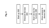
- FIG. 3 shows a flowchart of an approach for configuring devices for a multiprocessor system according to some embodiments.
- Some embodiments are directed to an improved approach for configuring devices for a multiprocessor system, where the devices pertaining to the different processors are viewed as connecting to a standardized common bus. Regardless of the specific processor to which a device is directly connected, that device can be generally identified and accessed along the standardized common bus. A common set of storage is employed to store the necessary information to utilize these devices via the common bus.
- the devices are configured as Peripheral Component Interconnect Express (PCIe) devices on a given processor chip.
- PCIe Peripheral Component Interconnect Express
- PCIe is an expansion card and interconnect bus standard that has been adopted to provide connectivity for hardware devices on a computer system.
- the PCIe bus serves as the primary motherboard-level interconnect that connects a host system processor with both integrated peripherals and add-on peripherals/expansion cards.
- the PCIe bus provides high-speed connectivity with shared address/data lines using a point-to-point topology.
- communications are encapsulated into packets, where the packetizing and depacketizing of data and status-message traffic is handled by the transaction layer of the PCIe port that is controlled by a PCIe controller.
- PCIe devices communicate via a logical connection (an interconnect or link), where the link is a point-to-point communication channel between two PCIe ports.
- PCIe standard can be found in the PCI Local Bus Specification Revision 2.2 and PCI Express 2.0 Base Specification , which are maintained by the PCI-SIG (PCI Special Interest Group) and are available at http://www.pcisig.com, both of which are hereby incorporated by reference in their entirety.
- FIG. 1 depicts an example processing system 100 having multiple processor chips/nodes 0 , 1 , 2 , and 3 (hereinafter nodes 0 , 1 , 2 , and 3 ) that are interconnected in a mesh.
- the processor nodes 0 , 1 , 2 , and 3 communicate over interchip links (also referred to as interchip coherency links) 140 and 141 . While there are four processors shown in system 100 , it is noted that this number of processors is merely illustrative, and that the inventive concepts disclosed herein may be applied to any number of processors.
- the interchip links 140 and 141 (“ICI”) allow processor nodes 0 , 1 , 2 , and 3 to be connected together through an interconnect mechanism.
- each processor has three ICI interfaces for connecting to the three other devices in a 4-processor configuration.
- the interchip communications block of the processor nodes contains register fields that define the number (e.g., the rank or order) of each processor in the multiprocessor configuration, as well as the number of each interchip bus within a particular processor.
- the associated control word contains the destination node number, as well as the ICI interface number to which the destination node is attached. Hardware then routes the data to the appropriate interface.
- FIG. 2 shows a more detailed illustration of a multiprocessor system having the four processor nodes 0 , 1 , 2 , and 3 , where the processor nodes are interconnected with coherent interchip links 240 .
- Each processor node is associated with multiple devices.
- each processor node is associated with a ROM 250 , DRAM 252 , PCIe port(s) 254 , USB controller(s) 256 , SGMII/RGMII device(s) 258 , and other peripheral 260 that may be connected to a processor node.
- FIG. 3 shows a flowchart of an approach for configuring devices in a multiprocessor system (e.g., the system of FIGS. 1 and 2 ) according to one embodiment of the invention.
- the multiprocessor system is powered up.
- one of the processor nodes is designated as the master, and the other processor nodes are designated as slave nodes.
- processor node 0 may be designated as the master node and processor nodes 1 , 2 , and 3 may be designated as the slave nodes.
- the master processor node will include an onboard and/or attached memory that contains start up software while the slave nodes do not include this memory.
- the master node uses the software in its onboard/attached memory to engage in a boot up process. During this process, the master node will communicate across the interchip links to identify and start up each of the slave nodes.
- each discovered device for each processor node is scanned to identify the function of that device. If there are devices across a bridge, then those devices are also scanned to identify their functions.
- the discovery process (e.g., 304 and 306 ) is performed to determine if a given device exists in the system. Once it is determined that the device (e.g., I/O or accelerator) exists, then information is obtained that is utilized to allow access to the device, e.g., information from PCIe registers. Such information includes, for example, an interrupt entry identifier, a bandwidth weight entry, and a message queue identifier.
- the discovered devices have assigned (e.g., pre-assigned) device identifiers.
- device identifiers are assigned to each of the discovered devices.
- the devices are identified using a data tuple composed of (a) bus number; (b) device number; and (c) function number.
- the bus number identifies the common bus on which the devices, which are all treated as PCIe devices, are resident.
- each of the devices that are shown as being attached to the processor cores will be associated with the same logical bus (e.g., “PCI Bus 0 ”). Since the devices are actually attached to different processor nodes, PCI Bus 0 is not a single physical bus. Instead, the internal devices on the processor chips within the multiprocessor system logically constitute PCI Bus 0 . It is this view of a common logical bus that permits the software to transparently view, configure and access any of the devices in the multiprocessor system, even though those devices are physically associated with different processor nodes.
- the device number portion of the device identifier specifies the specific device number for the (apparent) PCIe device.
- the multiprocessor system implements a PCIE Root Complex (RC) where the device internal to the processor chip maps to a PCIE Device Function on Bus 0 in the RC.
- each processor node implements up to eight (apparent) PCIE devices. Therefore, Device 0 -Device 7 would correspond to the first processor node (processor node 0 ), Device 8 -Device 15 would correspond to the second processor node (processor node 1 ), Device 16 -Device 23 would correspond to the third processor node (processor node 2 ), and Device 24 -Device 31 would correspond to the fourth processor node (processor node 3 ).
- RC PCIE Root Complex
- the function number is the identifier associated with the specific function of a given device. Each function for a device is tied to a specific and recognized function number.
- the PCIe device supports 4 functions ( 0 - 3 ), with one function per PCIe link. Function 0 corresponds to PCIe link 0 , while function 3 corresponds to PCIe link 3 .
- the PCIe controller can then be used to access the device by referring to the appropriate device identifier.
- FIG. 4 shows an example chart 402 of PCIe device functions that may be implemented for a multiprocessor system.
- all devices are associated with the same PCI bus 0 .
- This chart 402 includes a column 404 to identify the function number of a given entry in the chart 402 .
- the type column 406 identifies whether a device is an endpoint or a bridge.
- the Class column 408 identifies the class code for an entry, where the class code provides a defined class for a given type of device, e.g., based on PCIe standard defined classes.
- the description column 410 provides a brief description for each device entry in the chart 402 .
- Each device number is associated with a separate section of chart 402 .
- section 420 pertains to devices for the first device number for each processor node (e.g., device number 0 for node 0 , device number 8 for node 1 , device number 16 for node 2 , and device number 24 for node 3 ).
- section 422 pertains to devices for the second device number for each processor node, e.g., device number 1 for node 0 , device number 9 for node 1 , device number 17 for node 2 , and device number 25 for node 3 (as shown in portion 440 ).
- section 424 pertains to devices for the third device number for each processor node, e.g., device number 2 for node 0 , device number 10 for node 1 , device number 18 for node 2 , and device number 26 for node 3 (as shown in portion 444 ).
- Each of the other sections 426 , 428 , 430 , 432 , and 434 pertain to the fourth, fifth, sixth, seventh, and eighth device numbers, respectively, for the processor nodes, where the specific device numbers are shown in portions 444 , 446 , 448 , 450 , and 452 .
- This chart 402 assumes that each of the processor nodes will include similar devices to one another. Therefore, the chart 402 can be used to refer to all of the devices for all of the processor nodes, where the same device on each processor node has the same bus number and function number, but will be associated with a different device number.
- Entry 460 in chart 402 contains information that can be used to refer to both of these devices.
- the device identifier would include the combination of the bus number (Bus 0 ), the device number for this node (device 2 ), and the function number ( 1 ).
- the device identifier would include the combination of the bus number (Bus 0 ), the device number for this node (device 10 ), and the function number ( 1 ).
- the difference in the identifier between these two devices is in the device number, where the specific device number for each node can be found in portion 442 of the chart 402 .
- entry 462 corresponds to a device to implement a networking engine
- entry 464 corresponds to a device to implement a packet ordering engine
- entry 466 corresponds to a message station device
- entry 468 corresponds to a dynamic memory access (DMA) engine
- entry 470 corresponds to a security engine
- entry 472 corresponds to a compression/decompression engine.
- DMA dynamic memory access
- FIG. 5 visually illustrates how the combination of bus number, device number, and function number from chart 402 maps to PCIe devices for an example processor node.
- each device is viewed as a PCIe device on the PCI bus 0 , which can then be accessed according to its device identifier.
- the example of FIG. 5 illustrates the devices for processor node 0 , which pertains to device number 0 -device number 7 .
- a similar illustration can be drawn with the specific device numbers for those nodes.
- FIG. 6 illustrates an architectural model that results from the above approach of configuring devices in a multiprocessor system in accordance with some embodiments.
- This figure shows two of the processor nodes in an example system, e.g., processor node 0 and processor node 1 .
- Processor node 0 is represented on the left portion of this figure and processor node 1 is represented on the right side of this figure.
- Each of the devices for the processor nodes 0 and 1 is viewed as a PCIe device on the common virtual PCI bus (Bus 0 ).
- devices 660 a are represented as attached to the PCI bus 0 using the combination of the bus number (bus 0 ), function numbers 662 a , and the device numbers assigned to node 0 (device numbers 0 , 2 , and 3 for the devices shown in this figure).
- devices 660 b are represented as attached to the virtual PCI bus 0 using the combination of the bus number (bus 0 ), function numbers 662 b , and the device numbers assigned to node 1 (device numbers 8 , 10 , and 11 for the devices shown in this figure).
- these device numbers would correspond to coherent interchip ports for device number 0 , PCIe ports for device number 2 , and USB ports for device number 3 .
- each node includes its own host bus (or other interconnection) to communicate between the internal components of the processor nodes.
- host bus 608 a is used to provide internal communications for node 0 between the node 0 CPU(s) 602 a , node 0 cache 604 a , node 0 memory 606 a , and the node 0 PCIe RC.
- a first bridge 610 a and a second bridge 612 a are used to communicate between the host bus 608 a and the PCIe RC.
- host bus 608 b is used to provide internal communications for node 1 between the node 1 CPU(s) 602 b , node 1 cache 604 b , node 1 memory 606 b , and the node 1 PCIe RC.
- a first bridge 610 b and a second bridge 612 b are used to communicate between the host bus 608 b and the PCIe RC.
- the PCIe interface connects internally to the multiprocessor system through a station on the I/O interconnect and a station on a messaging network. Accesses are performed by either direct access or through a message-based access. With a direct access, the CPU reads or writes to a defined memory address space range. An internal memory bridge detects the read or write request, forwarding the transaction to the PCIe controller, which generates the appropriate PCIe signaling to the required destination.
- the message-based approach may also be used, where messaging is performed through the PCIe controllers to communicate across the interchip links to complete transactions to and from the PCIe devices.
- the interrupt behavior of the PCIe interface is integrated into the multiprocessor system's interrupt-handling system, which provides delivery to the different processor nodes and/or to specific cores/threads within the processor nodes.
- the PCIe controller reports interrupts detected by each link. Interrupts are signaled through the virtual wire concept of the PCIe, where in-band messages carry interrupt information or by assertion of dedicated PCIe interrupt pins.
- the device identifier is used to provide internal configuration register access, where the combination of the bus number, device number, and function number that identifies the PCIe controller's own configuration space results in an internal configuration register access.
- the read or write command effectively reads or writes the on-chip configuration registers.
- PCIe is a suitable standardized bus type that can be employed, where the devices for each processor node are represented as PCIe devices. Therefore, in this embodiment, each of the devices would appear to the system software as a PCIe device.
- a PCIe controller can then be used to access the device by referring to the appropriate device identifier. This permits any device to be accessed on any of the processor nodes, without requiring separate and individualized configurations or drivers for each separate processor node.
Abstract
Description
Claims (35)
Priority Applications (1)
| Application Number | Priority Date | Filing Date | Title |
|---|---|---|---|
| US13/164,319 US8725919B1 (en) | 2011-06-20 | 2011-06-20 | Device configuration for multiprocessor systems |
Applications Claiming Priority (1)
| Application Number | Priority Date | Filing Date | Title |
|---|---|---|---|
| US13/164,319 US8725919B1 (en) | 2011-06-20 | 2011-06-20 | Device configuration for multiprocessor systems |
Publications (1)
| Publication Number | Publication Date |
|---|---|
| US8725919B1 true US8725919B1 (en) | 2014-05-13 |
Family
ID=50635781
Family Applications (1)
| Application Number | Title | Priority Date | Filing Date |
|---|---|---|---|
| US13/164,319 Active 2031-10-30 US8725919B1 (en) | 2011-06-20 | 2011-06-20 | Device configuration for multiprocessor systems |
Country Status (1)
| Country | Link |
|---|---|
| US (1) | US8725919B1 (en) |
Cited By (10)
| Publication number | Priority date | Publication date | Assignee | Title |
|---|---|---|---|---|
| US20130151903A1 (en) * | 2011-12-08 | 2013-06-13 | Sharp Kabushiki Kaisha | Image forming apparatus |
| US20150052281A1 (en) * | 2013-08-19 | 2015-02-19 | International Business Machines Corporation | Function transfer using virtualized mapping |
| US20150362980A1 (en) * | 2014-06-16 | 2015-12-17 | Apple Inc. | Always-On Processor as a Coprocessor |
| WO2017023678A1 (en) * | 2015-08-03 | 2017-02-09 | Marvell World Trade Ltd. | Systems and methods for implementing topoloby-based identification process in a mochi environment |
| US20170039152A1 (en) * | 2015-08-03 | 2017-02-09 | Marvell World Trade Ltd. | Systems and methods for implementing topology-based identification process in a mochi environment |
| US20190306055A1 (en) * | 2018-03-29 | 2019-10-03 | Alibaba Group Holding Limited | Efficient and reliable message channel between a host system and an integrated circuit acceleration system |
| CN110462598A (en) * | 2017-04-07 | 2019-11-15 | 松下知识产权经营株式会社 | Information processing unit |
| US10705960B2 (en) | 2012-12-28 | 2020-07-07 | Intel Corporation | Processors having virtually clustered cores and cache slices |
| US20210349777A1 (en) * | 2019-01-25 | 2021-11-11 | Huawei Technologies Co., Ltd. | Fault processing method, related device, and computer storage medium |
| CN114880977A (en) * | 2022-05-11 | 2022-08-09 | 北京百度网讯科技有限公司 | Software and hardware joint simulation system, method, device, equipment and storage medium |
Citations (9)
| Publication number | Priority date | Publication date | Assignee | Title |
|---|---|---|---|---|
| US20020016877A1 (en) * | 1997-11-19 | 2002-02-07 | Porterfield A. Kent | Computer system having peer-to-peer bus bridges and shadow configuration registers |
| US20060272015A1 (en) * | 2005-05-26 | 2006-11-30 | Frank Charles W | Virtual devices and virtual bus tunnels, modules and methods |
| US20080016405A1 (en) * | 2006-07-13 | 2008-01-17 | Nec Computertechno, Ltd. | Computer system which controls closing of bus |
| US20080137676A1 (en) * | 2006-12-06 | 2008-06-12 | William T Boyd | Bus/device/function translation within and routing of communications packets in a pci switched-fabric in a multi-host environment environment utilizing a root switch |
| US20080209099A1 (en) * | 2007-02-28 | 2008-08-28 | Kloeppner John R | Apparatus and methods for clustering multiple independent pci express hierarchies |
| US20080288661A1 (en) * | 2007-05-16 | 2008-11-20 | Michael Galles | Method and system to map virtual i/o devices and resources to a standard i/o bus |
| US20090077297A1 (en) * | 2007-09-14 | 2009-03-19 | Hongxiao Zhao | Method and system for dynamically reconfiguring PCIe-cardbus controllers |
| US20110106981A1 (en) * | 2009-11-03 | 2011-05-05 | Sun Microsystems, Inc. | Configuration space compaction |
| US20110119423A1 (en) * | 2009-11-18 | 2011-05-19 | Kishore Karagada R | Assignment of Resources in an Input/Output (I/O) Virtualization System |
-
2011
- 2011-06-20 US US13/164,319 patent/US8725919B1/en active Active
Patent Citations (9)
| Publication number | Priority date | Publication date | Assignee | Title |
|---|---|---|---|---|
| US20020016877A1 (en) * | 1997-11-19 | 2002-02-07 | Porterfield A. Kent | Computer system having peer-to-peer bus bridges and shadow configuration registers |
| US20060272015A1 (en) * | 2005-05-26 | 2006-11-30 | Frank Charles W | Virtual devices and virtual bus tunnels, modules and methods |
| US20080016405A1 (en) * | 2006-07-13 | 2008-01-17 | Nec Computertechno, Ltd. | Computer system which controls closing of bus |
| US20080137676A1 (en) * | 2006-12-06 | 2008-06-12 | William T Boyd | Bus/device/function translation within and routing of communications packets in a pci switched-fabric in a multi-host environment environment utilizing a root switch |
| US20080209099A1 (en) * | 2007-02-28 | 2008-08-28 | Kloeppner John R | Apparatus and methods for clustering multiple independent pci express hierarchies |
| US20080288661A1 (en) * | 2007-05-16 | 2008-11-20 | Michael Galles | Method and system to map virtual i/o devices and resources to a standard i/o bus |
| US20090077297A1 (en) * | 2007-09-14 | 2009-03-19 | Hongxiao Zhao | Method and system for dynamically reconfiguring PCIe-cardbus controllers |
| US20110106981A1 (en) * | 2009-11-03 | 2011-05-05 | Sun Microsystems, Inc. | Configuration space compaction |
| US20110119423A1 (en) * | 2009-11-18 | 2011-05-19 | Kishore Karagada R | Assignment of Resources in an Input/Output (I/O) Virtualization System |
Non-Patent Citations (2)
| Title |
|---|
| PCI Express Base Specification Revision 2.1, PCI-SIG, pp. 1-704, Mar. 4, 2009. |
| PCI Local Bus Specification Revision 2.2, PCI Special Interest Group, pp. i-xx and 1-302, Dec. 18, 1998. |
Cited By (20)
| Publication number | Priority date | Publication date | Assignee | Title |
|---|---|---|---|---|
| US20130151903A1 (en) * | 2011-12-08 | 2013-06-13 | Sharp Kabushiki Kaisha | Image forming apparatus |
| US10705960B2 (en) | 2012-12-28 | 2020-07-07 | Intel Corporation | Processors having virtually clustered cores and cache slices |
| US10725919B2 (en) | 2012-12-28 | 2020-07-28 | Intel Corporation | Processors having virtually clustered cores and cache slices |
| US10725920B2 (en) * | 2012-12-28 | 2020-07-28 | Intel Corporation | Processors having virtually clustered cores and cache slices |
| US20150052281A1 (en) * | 2013-08-19 | 2015-02-19 | International Business Machines Corporation | Function transfer using virtualized mapping |
| US9032122B2 (en) * | 2013-08-19 | 2015-05-12 | International Business Machines Corporation | Function transfer using virtualized mapping |
| US9256559B2 (en) | 2013-08-19 | 2016-02-09 | International Business Machines Corporation | Function transfer using virtualized mapping |
| US20150362980A1 (en) * | 2014-06-16 | 2015-12-17 | Apple Inc. | Always-On Processor as a Coprocessor |
| WO2017023678A1 (en) * | 2015-08-03 | 2017-02-09 | Marvell World Trade Ltd. | Systems and methods for implementing topoloby-based identification process in a mochi environment |
| US10474597B2 (en) | 2015-08-03 | 2019-11-12 | Marvell World Trade Ltd. | Systems and methods for performing unknown address discovery in a MoChi space |
| US10552350B2 (en) | 2015-08-03 | 2020-02-04 | Marvell World Trade Ltd. | Systems and methods for aggregating data packets in a mochi system |
| TWI695262B (en) * | 2015-08-03 | 2020-06-01 | 巴貝多商馬維爾國際貿易有限公司 | Systems and methods for implementing topology-based identification process in a mochi environment |
| US10339077B2 (en) * | 2015-08-03 | 2019-07-02 | Marvell World Trade Ltd. | Systems and methods for implementing topology-based identification process in a MoChi environment |
| US20170039152A1 (en) * | 2015-08-03 | 2017-02-09 | Marvell World Trade Ltd. | Systems and methods for implementing topology-based identification process in a mochi environment |
| CN110462598A (en) * | 2017-04-07 | 2019-11-15 | 松下知识产权经营株式会社 | Information processing unit |
| CN110462598B (en) * | 2017-04-07 | 2023-08-18 | 松下知识产权经营株式会社 | Information processing apparatus |
| US20190306055A1 (en) * | 2018-03-29 | 2019-10-03 | Alibaba Group Holding Limited | Efficient and reliable message channel between a host system and an integrated circuit acceleration system |
| CN111936982A (en) * | 2018-03-29 | 2020-11-13 | 阿里巴巴集团控股有限公司 | Efficient and reliable message tunneling between host system and integrated circuit acceleration system |
| US20210349777A1 (en) * | 2019-01-25 | 2021-11-11 | Huawei Technologies Co., Ltd. | Fault processing method, related device, and computer storage medium |
| CN114880977A (en) * | 2022-05-11 | 2022-08-09 | 北京百度网讯科技有限公司 | Software and hardware joint simulation system, method, device, equipment and storage medium |
Similar Documents
| Publication | Publication Date | Title |
|---|---|---|
| US8725919B1 (en) | Device configuration for multiprocessor systems | |
| US8683110B2 (en) | I/O system and I/O control method | |
| US10210120B2 (en) | Method, apparatus and system to implement secondary bus functionality via a reconfigurable virtual switch | |
| KR101324844B1 (en) | System and method for transforming pcie sr-iov functions to appear as legacy functions | |
| US20070263642A1 (en) | Mechanism to flexibly support multiple device numbers on point-to-point interconnect upstream ports | |
| US20040015628A1 (en) | Interrupt handling in systems having multiple multi-processor clusters | |
| JP3807250B2 (en) | Cluster system, computer and program | |
| US8972611B2 (en) | Multi-server consolidated input/output (IO) device | |
| GB2460735A (en) | Bus Fabric for Embedded System Comprising Peer-to-Peer Communication Matrix | |
| US11829309B2 (en) | Data forwarding chip and server | |
| US20140173167A1 (en) | Pci express switch and computer system using the same | |
| US11714776B2 (en) | Enabling a multi-chip daisy chain topology using peripheral component interconnect express (PCIe) | |
| US11403250B2 (en) | Operation accelerator, switch, task scheduling method, and processing system | |
| US20220327080A1 (en) | PCIe DEVICE AND OPERATING METHOD THEREOF | |
| EP3716084A1 (en) | Apparatus and method for sharing a flash device among multiple masters of a computing platform | |
| US11928070B2 (en) | PCIe device | |
| US20220327081A1 (en) | PCIe DEVICE AND OPERATING METHOD THEREOF | |
| US11604742B2 (en) | Independent central processing unit (CPU) networking using an intermediate device | |
| TW200407712A (en) | Configurable multi-port multi-protocol network interface to support packet processing | |
| JP2004133942A (en) | Data bus system and inter-bus crossing accessing method | |
| US20130311699A1 (en) | Operations using direct memory access | |
| US20110138161A1 (en) | Input/output device including a host interface for processing function level reset requests in a specified time | |
| CN111190840A (en) | Multi-party central processing unit communication architecture based on field programmable gate array control | |
| KR20050080704A (en) | Apparatus and method of inter processor communication | |
| CN114915499A (en) | Data transmission method, related device, system and computer readable storage medium |
Legal Events
| Date | Code | Title | Description |
|---|---|---|---|
| AS | Assignment |
Owner name: NETLOGIC MICROSYSTEMS, INC., CALIFORNIA Free format text: ASSIGNMENT OF ASSIGNORS INTEREST;ASSIGNORS:ZHU, JULIANNE J.;HASS, DAVID T.;REEL/FRAME:026780/0980 Effective date: 20110808 |
|
| STCF | Information on status: patent grant |
Free format text: PATENTED CASE |
|
| AS | Assignment |
Owner name: NETLOGIC I LLC, DELAWARE Free format text: CHANGE OF NAME;ASSIGNOR:NETLOGIC MICROSYSTEMS, INC.;REEL/FRAME:035443/0824 Effective date: 20130123 Owner name: BROADCOM CORPORATION, CALIFORNIA Free format text: ASSIGNMENT OF ASSIGNORS INTEREST;ASSIGNOR:NETLOGIC I LLC;REEL/FRAME:035443/0763 Effective date: 20150327 |
|
| AS | Assignment |
Owner name: BANK OF AMERICA, N.A., AS COLLATERAL AGENT, NORTH CAROLINA Free format text: PATENT SECURITY AGREEMENT;ASSIGNOR:BROADCOM CORPORATION;REEL/FRAME:037806/0001 Effective date: 20160201 Owner name: BANK OF AMERICA, N.A., AS COLLATERAL AGENT, NORTH Free format text: PATENT SECURITY AGREEMENT;ASSIGNOR:BROADCOM CORPORATION;REEL/FRAME:037806/0001 Effective date: 20160201 |
|
| AS | Assignment |
Owner name: AVAGO TECHNOLOGIES GENERAL IP (SINGAPORE) PTE. LTD., SINGAPORE Free format text: ASSIGNMENT OF ASSIGNORS INTEREST;ASSIGNOR:BROADCOM CORPORATION;REEL/FRAME:041706/0001 Effective date: 20170120 Owner name: AVAGO TECHNOLOGIES GENERAL IP (SINGAPORE) PTE. LTD Free format text: ASSIGNMENT OF ASSIGNORS INTEREST;ASSIGNOR:BROADCOM CORPORATION;REEL/FRAME:041706/0001 Effective date: 20170120 |
|
| AS | Assignment |
Owner name: BROADCOM CORPORATION, CALIFORNIA Free format text: TERMINATION AND RELEASE OF SECURITY INTEREST IN PATENTS;ASSIGNOR:BANK OF AMERICA, N.A., AS COLLATERAL AGENT;REEL/FRAME:041712/0001 Effective date: 20170119 |
|
| MAFP | Maintenance fee payment |
Free format text: PAYMENT OF MAINTENANCE FEE, 4TH YEAR, LARGE ENTITY (ORIGINAL EVENT CODE: M1551) Year of fee payment: 4 |
|
| AS | Assignment |
Owner name: AVAGO TECHNOLOGIES INTERNATIONAL SALES PTE. LIMITE Free format text: MERGER;ASSIGNOR:AVAGO TECHNOLOGIES GENERAL IP (SINGAPORE) PTE. LTD.;REEL/FRAME:047230/0910 Effective date: 20180509 |
|
| AS | Assignment |
Owner name: AVAGO TECHNOLOGIES INTERNATIONAL SALES PTE. LIMITE Free format text: CORRECTIVE ASSIGNMENT TO CORRECT THE EFFECTIVE DATE OF THE MERGER PREVIOUSLY RECORDED AT REEL: 047230 FRAME: 0910. ASSIGNOR(S) HEREBY CONFIRMS THE MERGER;ASSIGNOR:AVAGO TECHNOLOGIES GENERAL IP (SINGAPORE) PTE. LTD.;REEL/FRAME:047351/0384 Effective date: 20180905 |
|
| AS | Assignment |
Owner name: AVAGO TECHNOLOGIES INTERNATIONAL SALES PTE. LIMITE Free format text: CORRECTIVE ASSIGNMENT TO CORRECT THE ERROR IN RECORDING THE MERGER IN THE INCORRECT US PATENT NO. 8,876,094 PREVIOUSLY RECORDED ON REEL 047351 FRAME 0384. ASSIGNOR(S) HEREBY CONFIRMS THE MERGER;ASSIGNOR:AVAGO TECHNOLOGIES GENERAL IP (SINGAPORE) PTE. LTD.;REEL/FRAME:049248/0558 Effective date: 20180905 |
|
| MAFP | Maintenance fee payment |
Free format text: PAYMENT OF MAINTENANCE FEE, 8TH YEAR, LARGE ENTITY (ORIGINAL EVENT CODE: M1552); ENTITY STATUS OF PATENT OWNER: LARGE ENTITY Year of fee payment: 8 |