US8724006B2 - Focal plane coding for digital imaging - Google Patents
Focal plane coding for digital imaging Download PDFInfo
- Publication number
- US8724006B2 US8724006B2 US10/784,472 US78447204A US8724006B2 US 8724006 B2 US8724006 B2 US 8724006B2 US 78447204 A US78447204 A US 78447204A US 8724006 B2 US8724006 B2 US 8724006B2
- Authority
- US
- United States
- Prior art keywords
- imaging system
- recited
- image
- lens
- pixel
- Prior art date
- Legal status (The legal status is an assumption and is not a legal conclusion. Google has not performed a legal analysis and makes no representation as to the accuracy of the status listed.)
- Expired - Fee Related, expires
Links
Images


Classifications
-
- H—ELECTRICITY
- H04—ELECTRIC COMMUNICATION TECHNIQUE
- H04N—PICTORIAL COMMUNICATION, e.g. TELEVISION
- H04N25/00—Circuitry of solid-state image sensors [SSIS]; Control thereof
- H04N25/48—Increasing resolution by shifting the sensor relative to the scene
Definitions
- ⁇ p / ⁇ ⁇ N.A.p/ ⁇ .
- the angular resolution is inversely proportional to f, meaning that the thicker the system, the better the angular resolution.
- the size and number of pixels determine the spatial resolution.
- Desired advances include reducing camera thickness, improving resolution and improving data efficiency.
- ICIS integrated computational imaging systems
- the design of ICIS simultaneously considers optics, optoelectronics and signal processing, rather than independently designing the optics.
- System performance for the ICIS is realized through joint optimization of optics, focal plane optoelectronics and post-detection algorithms.
- the computational imaging used to balance processing between optics and electronics are typically classified into three categories: wavefront encoding, multiplex imaging and feature extraction.
- Wavefront encoding involves modifying the wavefront phase at or near the pupil plane of an imaging system.
- multiplex imaging typically the optics introduce redundant information used in post-processing detection.
- feature extraction estimates are made of transform coefficients that are then used to make a decision. Often, all three categories are employed.
- ICIS use non-focal sensors, e.g., interferometric systems, wavefront coded systems.
- non-focal sensors e.g., interferometric systems, wavefront coded systems.
- the purposeful blurring attendant with such non-focal sensors which is then removed in post-processing, provides multiplexing in the optical field.
- this blurring does not exploit the point of high field entropy of the system.
- highest entropy is at the focal plane.
- the detectors of these systems are acting as pixel sensors rather than image sensors.
- At least one of the above and other features may be realized by applying ICIS at the focal plane of the imaging system.
- At least one of the above and other features may be realized by multiplexing in the electrical plane.
- At least one of the above and other features may be realized by providing an imaging system including an array of lenses, a plurality of sensor pixels for each lens, the sensor pixels being on an image plane of the imaging system, and a corresponding plurality of focal plane coding elements.
- a focal plane coding element for each sensor pixel has multiple sub-pixel resolution elements.
- the focal plane coding element being between the lens and each sensor pixel, wherein sub-pixel resolution elements over the plurality of focal plane coding elements represent a selected transform matrix having a non-zero determinant.
- the output of the plurality of sensor pixels being an image multiplied by this matrix.
- the filter may provide sub-pixel shifted multiple images on each sensor pixel.
- the focal plane coding element may be an apertured mask.
- the imaging system may include color filters, which may be integral with the focal plane coding element.
- a birefringent structure may be adjacent the focal plane coding element.
- a corresponding plurality of focusing lenses may be included between the focal plane encoding element and a corresponding sensor pixel.
- the selected transform matrix has fewer rows than columns. At least one sensor pixel receives light from more than one lens of the array of lenses.
- a processor receiving the outputs of the sensor pixels and multiplying the outputs by an inverse matrix may be included.
- the processor may reconstruct an image from the outputs, a number of image pixels in the image being greater than the plurality of sensor pixels.
- At least one of the above and other features may be realized by providing an imaging system including an array of lenses, a plurality of sensor pixels for each lens, a corresponding plurality of filters, and a processor.
- a filter for each sensor pixel has multiple sub-pixel resolution elements and provides a sub-pixel shifted multiple image on each sensor pixel.
- the processor receives outputs from each sensor pixel and reconstructs an image, a number of image pixels in the image being greater than the plurality of sensor pixels.
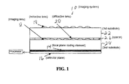
- FIG. 1 is a schematic side view of an array of micro-cameras according to an embodiment of the present invention
- FIG. 2 is an example of a mask to be used as a focal plane coding element in accordance with an embodiment of the present invention.
- FIG. 3 is a schematic side view of an array of micro-cameras according to another embodiment of the present invention.
- FIG. 1 illustrates a multiple aperture imaging system 10 .
- Each aperture includes an imaging lens 12 , a focal plane coding element 14 and a detector plane 16 .
- the detector plane 16 is located at or near the image plane of the system 10 .
- the detector plane 16 for each aperture includes a plurality of pixels in accordance with a size of an image at the image plane and the selected detector size.
- each aperture may include a plurality of substrates 22 , 24 , which may be separated by a spacer 26 .
- the spacer 26 may be integral with one of the substrates 22 , 24 or may be formed on a separate spacer substrate.
- a first refractive lens 18 is on a top surface of the substrate 22
- a diffractive lens is on a bottom surface of the substrate 22
- the imaging lens 12 is on a top surface of the substrate 24 .
- the diffractive lens 20 may correct for aberrations.
- the focal plane coding element 14 is provided on or adjacent to a bottom surface of the substrate 24 and the detector plane 16 is provided on or adjacent to the focal plane coding element 52 .
- Additional substrates providing additional surfaces with optical power therein may be provided in a similar fashion as dictated by the requirements of the system 10 .
- the substrates 22 and 24 may have surfaces parallel with one another and may be bonded together across the system 10 as shown in FIG. 1 .
- the focal plane coding element 14 samples and/or remaps the focused image for coded multiplexing at the optical-electronic interface.
- the outputs of the detector plane are provided to a processor 30 , which electrically process the information as discussed below.
- a processor 30 which electrically process the information as discussed below.
- there is no multiplexing of the optical field since the image is isomorphic and well focused at the focal plane. Rather, multiplexing occurs from the pixels sampling multiple optical resolution elements.
- the focal plane coding is to maintain the focal distribution while remapping sampling across the image plane to enable digital reconstruction of the image.
- a pixel measurement m may be modeled as in Equation (1):
- the pixel measurement is given by Equation (2): m ij ⁇ p ij ( r ) I ( r ) dr (2) where p ij (r) is the focal plane code in the focal plane coding element 14 for the i th pixel in the j th aperture of the multi-aperture system 10 .
- Compressive imaging uses focal plane coding to allow reconstruction of images having a higher spatial resolution than the number of pixels, i.e., detector elements, on the focal plane. In other words, if the number of image pixels is greater than the number of physical pixels.
- the rectangular transform may be non-local and non-convex. Different known rectangular transforms may be used, such as Hadamard, discrete cosine and quantized cosine, in which the discrete consine transform is rounded to correspond to a value in the set of the quantized cosine transform.
- transforms provide multiple lower resolution, i.e., pixel level, shifted with sub-pixel accuracy which are detected to recover a single higher resolution, i.e., sub-pixel level, image.
- the multiplexing is done at the electrical plane, since each detector samples multiple resolution elements.
- the outputs of the detector plane 16 to a processor or electrical plane 30 are not the image itself, but a matrix multiple of the image. Any appropriate matrix may be used, as long as the determinant of the matrix is not zero. Preferably, the matrix will allow as much power as possible on each pixel through to the detector plane 16 .
- the processor may then take the inverse matrix transform to retrieve the image.
- the focal plane coding element may be created having the focal plane code p ij (r) in accordance with H.
- An inverse transform H ⁇ 1 is applied by the processor 30 to the measurement m detected at the detecting plane 16 to get the estimated image.
- the difference between the estimated image and the real image is the noise of the system 10 .
- Different mechanisms may be used to realize physical implementation of the focal plane coding element 14 to provide multiple optical resolution elements for each detector.
- One such mechanism is coded masks created in accordance with the transform matrix selected. Such masks may include opaque amplitude patterns on optical transparent materials. These patterns may also be combined with surface relief structures to provide both phase and amplitude mapping. Breaking the image into sub-blocks, the transformation may be implemented on each sub-block.
- FIG. 2 An example of a mask pattern for a 4 ⁇ 4 sub-block is shown in FIG. 2 .
- the particular transform H in this example is a Hadamard-S matrix, which is a [0,1] matrix obtained by shifting the Hadamard matrix elementwise up by one and scaling it by half.
- a pixel filter 40 of the focal plane coding element 14 here a mask pattern, corresponding to each pixel is segmented into a 4 ⁇ 4 grid of optical resolution elements or apertures 42 , where a value of one is represented as white and a value of zero is represented as black.
- FIG. 2 shows the mask pattern for a particular matrix for Equation (3).
- Each 4 ⁇ 4 sub-pattern is placed over each pixel.
- each pixel receives a different portion of the image.
- each corresponding receives identical or nearly identical images.
- FIG. 2 shows the mask patterns on each of these corresponding pixels over the camera array. That is, each of these corresponding pixels in different micro-cameras, that receive near identical images, will be multiplied a different 4 ⁇ 4 sub-pattern. This may be most readily achieved by providing a same sub-pattern for each pixel in a given micro-camera. Over the array of micro-camera, each pixel may be multiplied by each 4 ⁇ 4 sub-pattern.
- each optical resolution element 42 will multiply the image with the matrix component for that optical resolution element 42 .
- the amount of power incident on each pixel should be maximized. This may be realized by examining the pixel with least amount of power thereon and altering the matrix to optimize this pixel while still keeping the determinant non-zero. Such optimization may be iterative.
- each pixel receives light from an area 40 including a plurality, here 4 ⁇ 4, optical resolution elements 42 . More generally, each pixel has a size p x p y , and each pixel filter 40 has a size d x d y with a plurality of m x m y optical resolution elements 42 of size q x q y . Normally, such a camera would have a resolution of 1/p x ⁇ 1/p y .
- the size of the pixel region 40 d x d y may be the same as or greater than the pixel size P x P y .
- the power incident on each pixel is equal to a summation, over all optical resolution elements 42 on the corresponding pixel filter 40 , of the power on each optical resolution elements 42 multiplied by the transmittance of the optical resolution elements 42 .
- the resolution of the camera may now be as low as 1/q x ⁇ 1/q y
- Additional distribution of the image onto the pixels may be combined with these masks to allow remapping of the image.
- separating of the image into vertical and horizontal polarization modes can be used to create coding elements that displace focal images across the image plane without diffraction.
- a suitable birefringent material is available in the wavelength region of interest, this material may be used for the mask. If this is not practical, subwavelength structures presenting different effective indices of refraction for the vertical and horizontal polarization states may be incorporated.
- Color images may be realized with the system 10 by placing different color filters in the path of different elements in the detection plane 16 .
- three color filters e.g. red, green and blue, are required, so each color filter may be in a path of a third of the macro-pixels. Since the eye is more sensitive to green, in many cases more green filters are used than red and blue, e.g. 25% of the pixels have blue and red filters and 75% have green filters
- color sensitive rather than binary absorption masks may be used as the coding elements in the focal plane coding element 16 . Since a color filter for a given wavelength will absorb most of the other wavelengths, this color filter can serve as providing a value of one (or high transmittance) for the design wavelength and a value of zero (or low transmittance) for other wavelengths.
- FIG. 3 Another imaging system 50 is shown in FIG. 3 .
- sensors in a detector plane 56 are too far from the focal plane coding element 14 to receive all of the light transmitted therefrom.
- another array of lenses 52 is provided for imaging the output of the focal plane coding element 14 onto the sensors in the detector plane 56 .
- compressive coding may also be used.
- compressive system design unimportant coefficients of the coefficient vector m are discarded, thus turning the corresponding row in the transform matrix H to 0. Therefore, fewer pixels may need to be employed, i.e., no physical implementation of these pixels for the discarded terms is required.
- the number of electronically generated image pixels is greater than the number of physical pixels.
- the compression ratio is defined by the number of rows to the number of columns in the transform matrix
- the above coding has assumed a transform matrix having elements from the set (1, 0).
- Transform matrices having elements from other sets, e.g., (1, ⁇ 1, 0) may be used.
- a threshold t is established. Any element having a value greater than t is set to 1, any element having a value less than ⁇ t is set to ⁇ 1 and all others are set to 0. Any threshold with an acceptable condition number for the matrix transform may be used.
- Such matrices may be implemented using photonic crystals or a combination of amplitude and phase masks.
- focal plane coding uses optical elements to encode digital imaging systems such that the spatial resolution of the reconstructed image exceeds the nominal spatial resolution of the electronic focal plane.
- Focal plane coding may be used to make cameras thinner than existing cameras while maintaining resolution and/or to improve resolution and data efficiency of digital imaging systems.
Abstract
Description
where A is the area of the pixel and I is the intensity.
m ij ∫p ij(r)I(r)dr (2)
where pij(r) is the focal plane code in the focal
m=Hs (3)
where s is the source or actual image and H is a rectangular transform. The rectangular transform may be non-local and non-convex. Different known rectangular transforms may be used, such as Hadamard, discrete cosine and quantized cosine, in which the discrete consine transform is rounded to correspond to a value in the set of the quantized cosine transform.
Claims (40)
Priority Applications (1)
| Application Number | Priority Date | Filing Date | Title |
|---|---|---|---|
| US10/784,472 US8724006B2 (en) | 2004-01-26 | 2004-02-24 | Focal plane coding for digital imaging |
Applications Claiming Priority (2)
| Application Number | Priority Date | Filing Date | Title |
|---|---|---|---|
| US53850604P | 2004-01-26 | 2004-01-26 | |
| US10/784,472 US8724006B2 (en) | 2004-01-26 | 2004-02-24 | Focal plane coding for digital imaging |
Publications (2)
| Publication Number | Publication Date |
|---|---|
| US20050162539A1 US20050162539A1 (en) | 2005-07-28 |
| US8724006B2 true US8724006B2 (en) | 2014-05-13 |
Family
ID=34798891
Family Applications (1)
| Application Number | Title | Priority Date | Filing Date |
|---|---|---|---|
| US10/784,472 Expired - Fee Related US8724006B2 (en) | 2004-01-26 | 2004-02-24 | Focal plane coding for digital imaging |
Country Status (1)
| Country | Link |
|---|---|
| US (1) | US8724006B2 (en) |
Cited By (3)
| Publication number | Priority date | Publication date | Assignee | Title |
|---|---|---|---|---|
| US20140191113A1 (en) * | 2013-01-04 | 2014-07-10 | California Institute Of Technology | System and method for color imaging with integrated plasmonic color filters |
| US11595575B2 (en) | 2020-05-11 | 2023-02-28 | Samsung Electronics Co., Ltd. | Image sensor |
| US11714987B2 (en) * | 2018-08-17 | 2023-08-01 | Fraunhofer-Gesellschaft zur Förderung der angewandten Forschung e.V. | Identification device, identification system and method for identifying an object |
Families Citing this family (6)
| Publication number | Priority date | Publication date | Assignee | Title |
|---|---|---|---|---|
| US20060057765A1 (en) * | 2004-09-13 | 2006-03-16 | Taiwan Semiconductor Manufacturing Company, Ltd. | Image sensor including multiple lenses and method of manufacture thereof |
| KR100821346B1 (en) * | 2006-08-02 | 2008-04-10 | 삼성전자주식회사 | Image sensor for improving the image quality and method of sensing the image for improving it |
| US7626150B2 (en) * | 2007-03-05 | 2009-12-01 | Raytheon Company | System and method for capturing image data over a wide field of view with high resolution |
| US20080219579A1 (en) * | 2007-03-05 | 2008-09-11 | Aksyuk Vladimir A | Methods and Apparatus for Compressed Imaging Using Modulation in Pupil Plane |
| EP2133726B1 (en) * | 2008-06-10 | 2011-06-01 | Thomson Licensing | Multi-image capture system with improved depth image resolution |
| RU2724151C1 (en) * | 2019-12-23 | 2020-06-22 | Олег Вадимович Смынтына | Method of increasing resolution of images obtained using matrix photodetectors |
Citations (36)
| Publication number | Priority date | Publication date | Assignee | Title |
|---|---|---|---|---|
| US4479143A (en) | 1980-12-16 | 1984-10-23 | Sharp Kabushiki Kaisha | Color imaging array and color imaging device |
| US4804249A (en) | 1986-12-24 | 1989-02-14 | Honeywell Inc. | Optical filter for incoherent imaging systems |
| US5355222A (en) * | 1992-05-15 | 1994-10-11 | Precision Tracking Fm, Inc. | Optical receiver for area location system |
| US5568197A (en) | 1991-04-08 | 1996-10-22 | Canon Kabushiki Kaisha | Camera apparatus having an optical low-pass filter |
| US5671073A (en) | 1995-02-15 | 1997-09-23 | California Institute Of Technology | Holographic storage using shift multiplexing |
| US5748371A (en) | 1995-02-03 | 1998-05-05 | The Regents Of The University Of Colorado | Extended depth of field optical systems |
| US5757423A (en) | 1993-10-22 | 1998-05-26 | Canon Kabushiki Kaisha | Image taking apparatus |
| US5760832A (en) | 1994-12-16 | 1998-06-02 | Minolta Co., Ltd. | Multiple imager with shutter control |
| US6069738A (en) | 1998-05-27 | 2000-05-30 | University Technology Corporation | Apparatus and methods for extending depth of field in image projection systems |
| US6137535A (en) * | 1996-11-04 | 2000-10-24 | Eastman Kodak Company | Compact digital camera with segmented fields of view |
| WO2001099431A2 (en) | 2000-06-16 | 2001-12-27 | University Technology Corporation | Method and apparatus for increasing resolution in digital imaging system by offsetting pixels |
| US6346969B1 (en) | 1996-12-30 | 2002-02-12 | Hyundai Electronics Industries Co., Ltd. | Color filter array and its color interpolation apparatus |
| US6366319B1 (en) * | 1997-07-03 | 2002-04-02 | Photronics Corp. | Subtractive color processing system for digital imaging |
| US6414296B1 (en) | 2000-09-21 | 2002-07-02 | Imation Corp. | Multiple pixel reading of holographic data including a position error calculation |
| US6417950B1 (en) | 2000-08-28 | 2002-07-09 | University Technology Corporation | Three-color imaging on each pixel for increased resolution |
| US20020089596A1 (en) | 2000-12-28 | 2002-07-11 | Yasuo Suda | Image sensing apparatus |
| WO2002077695A1 (en) | 2001-03-21 | 2002-10-03 | The Regents Of The University Of Colorado | High-speed confocal microscope |
| US20020163582A1 (en) | 2001-05-04 | 2002-11-07 | Gruber Michael A. | Self-calibrating, digital, large format camera with single or mulitiple detector arrays and single or multiple optical systems |
| US20020181126A1 (en) | 1998-06-30 | 2002-12-05 | Kimihiko Nishioka | Variable optical-property element |
| US20020181123A1 (en) | 2001-06-04 | 2002-12-05 | Xiaofeng Han | Astigmatism correcting optical coupler |
| WO2003024090A1 (en) | 2001-09-07 | 2003-03-20 | Koninklijke Philips Electronics N.V. | Image device having camera and image perspective correction and possibly rotation and staggering correction |
| US6541284B2 (en) | 2000-05-23 | 2003-04-01 | Atmel Corporation | Integrated IC chip package for electronic image sensor die |
| US6611289B1 (en) | 1999-01-15 | 2003-08-26 | Yanbin Yu | Digital cameras using multiple sensors with multiple lenses |
| US6632701B2 (en) | 2000-09-25 | 2003-10-14 | Foveon, Inc. | Vertical color filter detector group and array |
| US20050073603A1 (en) * | 2003-10-01 | 2005-04-07 | Digital Optics Corporation | Thin camera having sub-pixel resolution |
| US6882364B1 (en) | 1997-12-02 | 2005-04-19 | Fuji Photo Film Co., Ltd | Solid-state imaging apparatus and signal processing method for transforming image signals output from a honeycomb arrangement to high quality video signals |
| WO2005041561A1 (en) | 2003-10-27 | 2005-05-06 | Koninklijke Philips Electronics N.V. | Camera module and manufacturing method for such a camera module |
| US20050104991A1 (en) | 1999-09-03 | 2005-05-19 | Sony Corporation | Imaging element, imaging device, camera module and camera system |
| US20050128335A1 (en) | 2003-12-11 | 2005-06-16 | Timo Kolehmainen | Imaging device |
| US20050242410A1 (en) | 2002-07-18 | 2005-11-03 | Koninklijke Philips Electronics N.V. | Camera module, holder for use in a camera module, camera system and method of manufacturing a camera module |
| US20050248680A1 (en) | 2004-05-04 | 2005-11-10 | Tessera, Inc. | Compact lens turret assembly |
| US20050258350A1 (en) | 2002-09-09 | 2005-11-24 | Koninklijke Philips Electronics, N.V. | Optoelectronic semiconductor device and method of manufacturing such a device |
| US7003177B1 (en) * | 1999-03-30 | 2006-02-21 | Ramot At Tel-Aviv University Ltd. | Method and system for super resolution |
| US20060044450A1 (en) | 2002-09-17 | 2006-03-02 | Koninklijke Philips Electronics, N.C. | Camera device, method of manufacturing a camera device, wafer scale package |
| US7009652B1 (en) * | 1999-08-20 | 2006-03-07 | Minolta Co. Ltd | Image input apparatus |
| US7034866B1 (en) | 2000-11-22 | 2006-04-25 | Koninklijke Philips Electronics N.V. | Combined display-camera for an image processing system |
-
2004
- 2004-02-24 US US10/784,472 patent/US8724006B2/en not_active Expired - Fee Related
Patent Citations (36)
| Publication number | Priority date | Publication date | Assignee | Title |
|---|---|---|---|---|
| US4479143A (en) | 1980-12-16 | 1984-10-23 | Sharp Kabushiki Kaisha | Color imaging array and color imaging device |
| US4804249A (en) | 1986-12-24 | 1989-02-14 | Honeywell Inc. | Optical filter for incoherent imaging systems |
| US5568197A (en) | 1991-04-08 | 1996-10-22 | Canon Kabushiki Kaisha | Camera apparatus having an optical low-pass filter |
| US5355222A (en) * | 1992-05-15 | 1994-10-11 | Precision Tracking Fm, Inc. | Optical receiver for area location system |
| US5757423A (en) | 1993-10-22 | 1998-05-26 | Canon Kabushiki Kaisha | Image taking apparatus |
| US5760832A (en) | 1994-12-16 | 1998-06-02 | Minolta Co., Ltd. | Multiple imager with shutter control |
| US5748371A (en) | 1995-02-03 | 1998-05-05 | The Regents Of The University Of Colorado | Extended depth of field optical systems |
| US5671073A (en) | 1995-02-15 | 1997-09-23 | California Institute Of Technology | Holographic storage using shift multiplexing |
| US6137535A (en) * | 1996-11-04 | 2000-10-24 | Eastman Kodak Company | Compact digital camera with segmented fields of view |
| US6346969B1 (en) | 1996-12-30 | 2002-02-12 | Hyundai Electronics Industries Co., Ltd. | Color filter array and its color interpolation apparatus |
| US6366319B1 (en) * | 1997-07-03 | 2002-04-02 | Photronics Corp. | Subtractive color processing system for digital imaging |
| US6882364B1 (en) | 1997-12-02 | 2005-04-19 | Fuji Photo Film Co., Ltd | Solid-state imaging apparatus and signal processing method for transforming image signals output from a honeycomb arrangement to high quality video signals |
| US6069738A (en) | 1998-05-27 | 2000-05-30 | University Technology Corporation | Apparatus and methods for extending depth of field in image projection systems |
| US20020181126A1 (en) | 1998-06-30 | 2002-12-05 | Kimihiko Nishioka | Variable optical-property element |
| US6611289B1 (en) | 1999-01-15 | 2003-08-26 | Yanbin Yu | Digital cameras using multiple sensors with multiple lenses |
| US7003177B1 (en) * | 1999-03-30 | 2006-02-21 | Ramot At Tel-Aviv University Ltd. | Method and system for super resolution |
| US7009652B1 (en) * | 1999-08-20 | 2006-03-07 | Minolta Co. Ltd | Image input apparatus |
| US20050104991A1 (en) | 1999-09-03 | 2005-05-19 | Sony Corporation | Imaging element, imaging device, camera module and camera system |
| US6541284B2 (en) | 2000-05-23 | 2003-04-01 | Atmel Corporation | Integrated IC chip package for electronic image sensor die |
| WO2001099431A2 (en) | 2000-06-16 | 2001-12-27 | University Technology Corporation | Method and apparatus for increasing resolution in digital imaging system by offsetting pixels |
| US6417950B1 (en) | 2000-08-28 | 2002-07-09 | University Technology Corporation | Three-color imaging on each pixel for increased resolution |
| US6414296B1 (en) | 2000-09-21 | 2002-07-02 | Imation Corp. | Multiple pixel reading of holographic data including a position error calculation |
| US6632701B2 (en) | 2000-09-25 | 2003-10-14 | Foveon, Inc. | Vertical color filter detector group and array |
| US7034866B1 (en) | 2000-11-22 | 2006-04-25 | Koninklijke Philips Electronics N.V. | Combined display-camera for an image processing system |
| US20020089596A1 (en) | 2000-12-28 | 2002-07-11 | Yasuo Suda | Image sensing apparatus |
| WO2002077695A1 (en) | 2001-03-21 | 2002-10-03 | The Regents Of The University Of Colorado | High-speed confocal microscope |
| US20020163582A1 (en) | 2001-05-04 | 2002-11-07 | Gruber Michael A. | Self-calibrating, digital, large format camera with single or mulitiple detector arrays and single or multiple optical systems |
| US20020181123A1 (en) | 2001-06-04 | 2002-12-05 | Xiaofeng Han | Astigmatism correcting optical coupler |
| WO2003024090A1 (en) | 2001-09-07 | 2003-03-20 | Koninklijke Philips Electronics N.V. | Image device having camera and image perspective correction and possibly rotation and staggering correction |
| US20050242410A1 (en) | 2002-07-18 | 2005-11-03 | Koninklijke Philips Electronics N.V. | Camera module, holder for use in a camera module, camera system and method of manufacturing a camera module |
| US20050258350A1 (en) | 2002-09-09 | 2005-11-24 | Koninklijke Philips Electronics, N.V. | Optoelectronic semiconductor device and method of manufacturing such a device |
| US20060044450A1 (en) | 2002-09-17 | 2006-03-02 | Koninklijke Philips Electronics, N.C. | Camera device, method of manufacturing a camera device, wafer scale package |
| US20050073603A1 (en) * | 2003-10-01 | 2005-04-07 | Digital Optics Corporation | Thin camera having sub-pixel resolution |
| WO2005041561A1 (en) | 2003-10-27 | 2005-05-06 | Koninklijke Philips Electronics N.V. | Camera module and manufacturing method for such a camera module |
| US20050128335A1 (en) | 2003-12-11 | 2005-06-16 | Timo Kolehmainen | Imaging device |
| US20050248680A1 (en) | 2004-05-04 | 2005-11-10 | Tessera, Inc. | Compact lens turret assembly |
Non-Patent Citations (7)
| Title |
|---|
| Applied Optics, vol. 40, No. 11, Apr. 10, 2001, "Thin observation module by bound optics (TOMOBO) concept and experimental verification". * |
| Dowski, Jr., et al., "Aberration Invariant Optical/Digital Incoherent Optical Systems" Imaging Systems Laboratory, Dept of Electrical Engineering, U. Colorado, Boulder CO. [Publisher, Date-unknown]. |
| Dowski, Jr., et al., "Wavefront Coding: A modern method of achieving high performance and/or low cost imaging systems", [Publisher, Date-unknown]. |
| Kubala, et al., "Reducing complexity in computational imaging systems", Optical Society of America, copyright 2003. |
| Mait, et al, "Evolutionary paths in imaging and recent trends", Optics Express vol. 11, No. 18, pp. 2093-2101 (Sep. 8, 2003). |
| Optics Express, vol. 11, No. 18, Sep. 8, 2003, "Color imaging with an integrated compound imaging system". * |
| Potuluri, et al., "High depth of field microscopic imaging using an interferometric camera", Optics Express, vol. 8, No. 11, pp. 624-630 (May 21, 2001). |
Cited By (4)
| Publication number | Priority date | Publication date | Assignee | Title |
|---|---|---|---|---|
| US20140191113A1 (en) * | 2013-01-04 | 2014-07-10 | California Institute Of Technology | System and method for color imaging with integrated plasmonic color filters |
| US9627434B2 (en) * | 2013-01-04 | 2017-04-18 | California Institute Of Technology | System and method for color imaging with integrated plasmonic color filters |
| US11714987B2 (en) * | 2018-08-17 | 2023-08-01 | Fraunhofer-Gesellschaft zur Förderung der angewandten Forschung e.V. | Identification device, identification system and method for identifying an object |
| US11595575B2 (en) | 2020-05-11 | 2023-02-28 | Samsung Electronics Co., Ltd. | Image sensor |
Also Published As
| Publication number | Publication date |
|---|---|
| US20050162539A1 (en) | 2005-07-28 |
Similar Documents
| Publication | Publication Date | Title |
|---|---|---|
| KR102391632B1 (en) | Light field imaging device and depth acquisition and three-dimensional imaging method | |
| US10306158B2 (en) | Infrared imaging system and method of operating | |
| US8325266B2 (en) | Method of forming thin camera | |
| US9756228B2 (en) | Low profile camera and vision sensor | |
| US7835002B2 (en) | System for multi- and hyperspectral imaging | |
| US11300449B2 (en) | Imaging device with image dispersing to create a spatially coded image | |
| EP2315448B1 (en) | Thin camera having sub-pixel resolution | |
| CN202454558U (en) | Solid photographic device and photographic equipment | |
| Antipa et al. | Single-shot diffuser-encoded light field imaging | |
| US20150234102A1 (en) | Dynamically focusable multispectral light field imaging | |
| KR20100122058A (en) | Two-dimensional solid-state image capture device and polarization-light data processing method therefor | |
| US10212401B2 (en) | Image generation device and imaging device | |
| US8724006B2 (en) | Focal plane coding for digital imaging | |
| US9425229B2 (en) | Solid-state imaging element, imaging device, and signal processing method including a dispersing element array and microlens array | |
| Horstmeyer et al. | Modified light field architecture for reconfigurable multimode imaging | |
| Pitsianis et al. | Compressive imaging sensors | |
| CN109417590B (en) | Plenoptic aperture view shuffling with improved resolution | |
| CN109792511B (en) | Full photon aperture view slippage for richer color sampling | |
| Brady et al. | Compressive optical MONTAGE photography | |
| Brady | Focal plane coding for digital imaging | |
| Gruev et al. | Advances in integrated polarization image sensors | |
| Lam | Compact and thin multi-lens system for machine vision applications | |
| KR20230127277A (en) | Imaging device and optical element | |
| Nordin et al. | Polarization sensitive diffractive optics for integration with infrared photodetector arrays |
Legal Events
| Date | Code | Title | Description |
|---|---|---|---|
| AS | Assignment |
Owner name: DIGITAL OPTICS CORPORATION, NORTH CAROLINA Free format text: ASSIGNMENT OF ASSIGNORS INTEREST;ASSIGNORS:BRADY, DAVID;FELDMAN, MICHAEL;PITSIANIS, NIKOS P.;SIGNING DATES FROM 20040624 TO 20040723;REEL/FRAME:025207/0650 Owner name: DUKE UNIVERSITY, NORTH CAROLINA Free format text: ASSIGNMENT OF ASSIGNORS INTEREST;ASSIGNORS:BRADY, DAVID;FELDMAN, MICHAEL;PITSIANIS, NIKOS P.;SIGNING DATES FROM 20040624 TO 20040723;REEL/FRAME:025207/0650 |
|
| AS | Assignment |
Owner name: TESSERA NORTH AMERICA, INC, NORTH CAROLINA Free format text: CHANGE OF NAME;ASSIGNOR:DIGITAL OPTICS CORPORATION;REEL/FRAME:025651/0206 Effective date: 20070330 |
|
| AS | Assignment |
Owner name: DIGITALOPTICS CORPORATION EAST, NORTH CAROLINA Free format text: CHANGE OF NAME;ASSIGNOR:TESSERA NORTH AMERICA, INC.;REEL/FRAME:027262/0380 Effective date: 20110701 |
|
| AS | Assignment |
Owner name: FLIR SYSTEMS TRADING BELGIUM BVBA, BELGIUM Free format text: ASSIGNMENT OF ASSIGNORS INTEREST;ASSIGNOR:DIGITALOPTICS CORPORATION EAST;REEL/FRAME:032827/0362 Effective date: 20130808 |
|
| FEPP | Fee payment procedure |
Free format text: MAINTENANCE FEE REMINDER MAILED (ORIGINAL EVENT CODE: REM.) |
|
| LAPS | Lapse for failure to pay maintenance fees |
Free format text: PATENT EXPIRED FOR FAILURE TO PAY MAINTENANCE FEES (ORIGINAL EVENT CODE: EXP.) |
|
| STCH | Information on status: patent discontinuation |
Free format text: PATENT EXPIRED DUE TO NONPAYMENT OF MAINTENANCE FEES UNDER 37 CFR 1.362 |