US8623686B2 - Microelectromechanical device including an encapsulation layer of which a portion is removed to expose a substantially planar surface having a portion that is disposed outside and above a chamber and including a field region on which integrated circuits are formed, and methods for fabricating same - Google Patents
Microelectromechanical device including an encapsulation layer of which a portion is removed to expose a substantially planar surface having a portion that is disposed outside and above a chamber and including a field region on which integrated circuits are formed, and methods for fabricating same Download PDFInfo
- Publication number
- US8623686B2 US8623686B2 US13/829,393 US201313829393A US8623686B2 US 8623686 B2 US8623686 B2 US 8623686B2 US 201313829393 A US201313829393 A US 201313829393A US 8623686 B2 US8623686 B2 US 8623686B2
- Authority
- US
- United States
- Prior art keywords
- encapsulation layer
- silicon
- chamber
- layer
- mechanical structure
- Prior art date
- Legal status (The legal status is an assumption and is not a legal conclusion. Google has not performed a legal analysis and makes no representation as to the accuracy of the status listed.)
- Expired - Lifetime
Links
Images


Classifications
-
- B—PERFORMING OPERATIONS; TRANSPORTING
- B81—MICROSTRUCTURAL TECHNOLOGY
- B81B—MICROSTRUCTURAL DEVICES OR SYSTEMS, e.g. MICROMECHANICAL DEVICES
- B81B7/00—Microstructural systems; Auxiliary parts of microstructural devices or systems
- B81B7/02—Microstructural systems; Auxiliary parts of microstructural devices or systems containing distinct electrical or optical devices of particular relevance for their function, e.g. microelectro-mechanical systems [MEMS]
-
- B—PERFORMING OPERATIONS; TRANSPORTING
- B81—MICROSTRUCTURAL TECHNOLOGY
- B81C—PROCESSES OR APPARATUS SPECIALLY ADAPTED FOR THE MANUFACTURE OR TREATMENT OF MICROSTRUCTURAL DEVICES OR SYSTEMS
- B81C1/00—Manufacture or treatment of devices or systems in or on a substrate
- B81C1/00015—Manufacture or treatment of devices or systems in or on a substrate for manufacturing microsystems
- B81C1/00261—Processes for packaging MEMS devices
- B81C1/00301—Connecting electric signal lines from the MEMS device with external electrical signal lines, e.g. through vias
-
- H—ELECTRICITY
- H01—ELECTRIC ELEMENTS
- H01L—SEMICONDUCTOR DEVICES NOT COVERED BY CLASS H10
- H01L21/00—Processes or apparatus adapted for the manufacture or treatment of semiconductor or solid state devices or of parts thereof
- H01L21/02—Manufacture or treatment of semiconductor devices or of parts thereof
- H01L21/04—Manufacture or treatment of semiconductor devices or of parts thereof the devices having at least one potential-jump barrier or surface barrier, e.g. PN junction, depletion layer or carrier concentration layer
- H01L21/34—Manufacture or treatment of semiconductor devices or of parts thereof the devices having at least one potential-jump barrier or surface barrier, e.g. PN junction, depletion layer or carrier concentration layer the devices having semiconductor bodies not provided for in groups H01L21/0405, H01L21/0445, H01L21/06, H01L21/16 and H01L21/18 with or without impurities, e.g. doping materials
- H01L21/44—Manufacture of electrodes on semiconductor bodies using processes or apparatus not provided for in groups H01L21/38 - H01L21/428
-
- B—PERFORMING OPERATIONS; TRANSPORTING
- B81—MICROSTRUCTURAL TECHNOLOGY
- B81B—MICROSTRUCTURAL DEVICES OR SYSTEMS, e.g. MICROMECHANICAL DEVICES
- B81B2207/00—Microstructural systems or auxiliary parts thereof
- B81B2207/01—Microstructural systems or auxiliary parts thereof comprising a micromechanical device connected to control or processing electronics, i.e. Smart-MEMS
- B81B2207/015—Microstructural systems or auxiliary parts thereof comprising a micromechanical device connected to control or processing electronics, i.e. Smart-MEMS the micromechanical device and the control or processing electronics being integrated on the same substrate
-
- B—PERFORMING OPERATIONS; TRANSPORTING
- B81—MICROSTRUCTURAL TECHNOLOGY
- B81C—PROCESSES OR APPARATUS SPECIALLY ADAPTED FOR THE MANUFACTURE OR TREATMENT OF MICROSTRUCTURAL DEVICES OR SYSTEMS
- B81C2201/00—Manufacture or treatment of microstructural devices or systems
- B81C2201/01—Manufacture or treatment of microstructural devices or systems in or on a substrate
- B81C2201/0174—Manufacture or treatment of microstructural devices or systems in or on a substrate for making multi-layered devices, film deposition or growing
- B81C2201/0176—Chemical vapour Deposition
-
- B—PERFORMING OPERATIONS; TRANSPORTING
- B81—MICROSTRUCTURAL TECHNOLOGY
- B81C—PROCESSES OR APPARATUS SPECIALLY ADAPTED FOR THE MANUFACTURE OR TREATMENT OF MICROSTRUCTURAL DEVICES OR SYSTEMS
- B81C2203/00—Forming microstructural systems
- B81C2203/01—Packaging MEMS
- B81C2203/0136—Growing or depositing of a covering layer
-
- H—ELECTRICITY
- H01—ELECTRIC ELEMENTS
- H01L—SEMICONDUCTOR DEVICES NOT COVERED BY CLASS H10
- H01L2924/00—Indexing scheme for arrangements or methods for connecting or disconnecting semiconductor or solid-state bodies as covered by H01L24/00
- H01L2924/0001—Technical content checked by a classifier
- H01L2924/0002—Not covered by any one of groups H01L24/00, H01L24/00 and H01L2224/00
Definitions
- This invention relates to electromechanical systems and techniques for fabricating microelectromechanical and nanoelectromechanical systems; and more particularly, in one aspect, to fabricating or manufacturing microelectromechanical and nanoelectromechanical systems with high performance integrated circuits on a common substrate.
- the mechanical structures are typically sealed in a chamber.
- the delicate mechanical structure may be sealed in, for example, a hermetically sealed metal container (for example, a TO-8 “can”, see, for example, U.S. Pat. No. 6,307,815) or bonded to a semiconductor or glass-like substrate having a chamber to house, accommodate or cover the mechanical structure (see, for example, U.S. Pat. Nos. 6,146,917; 6,352,935; 6,477,901; and 6,507,082).
- the substrate on, or in which, the mechanical structure resides may be disposed in and affixed to the metal container.
- the hermetically sealed metal container also serves as a primary package as well.
- MEMS that employ a hermetically sealed metal container or a bonded semiconductor or glass-like substrate to protect the mechanical structures tend to be difficult to cost effectively integrate with high performance integrated circuitry on the same substrate.
- the additional processing required to integrate the high performance integrated circuitry tends to either damage or destroy the mechanical structures.
- the mechanical structure is encapsulated in a chamber using a conventional oxide (SiO.sub.2) deposited or formed using conventional techniques (i.e., oxidation using low temperature techniques (LTO), tetraethoxysilane (TEOS) or the like).
- LTO low temperature techniques
- TEOS tetraethoxysilane
- the mechanical structure is encapsulated prior to packaging and/or integration with integrated circuitry.
- a conventional oxide to encapsulate the mechanical structures of the MEMS may provide advantages relative to hermetically sealed metal container or a bonded semiconductor or glass-like substrate
- a conventional oxide deposited using conventional techniques, often exhibits high tensile stress at, for example, corners or steps (i.e., significant spatial transitions in the underlying surface(s)). Further, such an oxide is often formed or deposited in a manner that provides poor coverage of those areas where the underlying surface(s) exhibit significant spatial transitions.
- a conventional oxide deposited using conventional techniques
- a conventional oxide often provides an insufficient vacuum where a vacuum is desired as the environment in which the mechanical structures are encapsulated and designed to operate.
- a conventional oxide deposited using conventional techniques, may produce a film on the mechanical structures during the encapsulation process. This film may impact the integrity of the mechanical structures and, as such, the performance or operating characteristics of the MEMS (for example, the operating characteristics of a resonator).
- the present invention is a method of sealing a chamber of an electromechanical device having a mechanical structure disposed within the chamber.
- the method includes depositing a sacrificial layer over at least a portion of the mechanical structure and depositing a first encapsulation layer (for example, a polycrystalline silicon, amorphous silicon, germanium, silicon/germanium or gallium arsenide) over the sacrificial layer. At least one vent is formed through the first encapsulation layer, and at least a portion of the sacrificial layer is removed to form the chamber.
- a first encapsulation layer for example, a polycrystalline silicon, amorphous silicon, germanium, silicon/germanium or gallium arsenide
- the method may also include planarizing an exposed surface of the second encapsulation layer and removing a sufficient amount of the second encapsulation layer to thereby expose the first encapsulation layer and provide junction isolation.
- a first portion of the first encapsulation layer is comprised of a monocrystalline silicon and a second portion is comprised of a polycrystalline silicon.
- a surface of the second encapsulation layer may be planarized to expose the first portion of the first encapsulation. Thereafter, a monocrystalline silicon may be grown on the first portion of the first encapsulation.
- the present invention is a method of manufacturing an electromechanical device having a mechanical structure that resides in a chamber.
- the chamber may include a fluid having a pressure that provides mechanical damping for the mechanical structure.
- the method comprises depositing a first encapsulation layer (comprised of a semiconductor material, for example, polycrystalline silicon, amorphous silicon, silicon carbide, silicon/germanium, germanium, or gallium arsenide) over the mechanical structure. At least one vent is then formed in the first encapsulation layer and the chamber is formed.
- a second encapsulation layer (comprised of a semiconductor material, for example, polycrystalline silicon, porous polycrystalline silicon, amorphous silicon, silicon carbide, silicon/germanium, germanium, or gallium arsenide) is deposited over or in the vent to seal the chamber.
- a semiconductor material for example, polycrystalline silicon, porous polycrystalline silicon, amorphous silicon, silicon carbide, silicon/germanium, germanium, or gallium arsenide
- the first encapsulation layer is doped with a first impurity to provide a first region of a first conductivity type
- the second encapsulation layer is doped with a second impurity to provide a second region with a second conductivity type.
- the first conductivity type is opposite the second conductivity type.
- the first and second encapsulation layers may be deposited using an epitaxial or a CVD reactor.
- a first portion of the first encapsulation layer is comprised of a monocrystalline silicon and a second portion is comprised of a polycrystalline silicon.
- a surface of the second encapsulation layer may be planarized to expose the first portion of the first encapsulation. Thereafter, a monocrystalline silicon may be grown on the first portion of the first encapsulation.
- the present invention is an electromechanical device comprising a chamber including a first encapsulation layer (for example, polycrystalline silicon, porous polycrystalline silicon, amorphous silicon, germanium, silicon/germanium, gallium arsenide, silicon nitride or silicon carbide), having at least one vent, and a mechanical structure having at least a portion disposed in the chamber.
- the electromechanical device also includes a second encapsulation layer comprised of a semiconductor material (for example, polycrystalline silicon, porous polycrystalline silicon, amorphous silicon, silicon carbide, silicon/germanium, germanium, or gallium arsenide), deposited over or in the vent, to thereby seal the chamber.
- the device may also include a contact (i.e., a conductive region, such as the contact area and/or contact via, that is partially or wholly disposed outside of the chamber) disposed outside the chamber.
- a contact i.e., a conductive region, such as the contact area and/or contact via, that is partially or wholly disposed outside of the chamber.
- the contact may be a semiconductor that is doped with impurities to increase the conductivity of the area.
- the contact may be surrounded by the semiconductor of the first conductivity type and the semiconductor of the second conductivity type, which, in combination, forms a junction isolation.
- the device of this aspect of the present invention may include a first portion of the first encapsulation layer that is comprised of a monocrystalline silicon and a second portion is comprised of a polycrystalline silicon.
- the present invention may include a field region disposed outside and above the chamber wherein the field region is comprised of a monocrystalline silicon.
- the first portion of the first encapsulation layer may be comprised of a monocrystalline silicon and a second portion comprised of a porous or amorphous silicon.
- the second encapsulation layer overlying the second portion of the first encapsulation layer is a polycrystalline silicon.
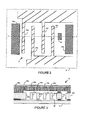
- FIG. 2 illustrates a top view of a portion of micromechanical structure, for example, or portion of the interdigitated or comb-like finger electrode arrays of an accelerometer, in conjunction with a contact area and field regions;
- FIG. 3 illustrates a cross-sectional view (sectioned along dotted line a-a of FIG. 2 ) of the portion of the interdigitated or comb-like finger electrode array and contact area and field regions of FIG. 2 , in accordance with certain aspects of the present invention
- FIGS. 5A-5C illustrate cross-sectional views of additional fabrication processes of the microstructure of FIG. 3 , according to certain aspects of the present invention
- FIGS. 6A-6F illustrate cross-sectional views of the fabrication of the microstructure, according to certain aspects of the present invention, at various stages of the process
- FIGS. 8A-8E illustrate cross-sectional views of the fabrication of the microstructure at various stages of an encapsulation process where the first encapsulation layer is a permeable material, according to certain aspects of the present invention
- FIG. 11A illustrates a cross-sectional view of a portion of a plurality of micromechanical structures, each having one or more electromechanical systems, which are monolithically integrated on or within the substrate of a MEMS, in accordance with certain aspect of the present invention
- FIG. 11B-11D illustrate cross-sectional views of a portion of a micromechanical structure, having a plurality of microstructures, which are monolithically integrated on or within the substrate of a MEMS, in accordance with certain aspect of the present invention
- FIG. 12A-12C illustrate cross-sectional views of MEMS, according to certain aspects of the present inventions, including a micromachined mechanical structure portion and an integrated circuit portion, both portions of which are disposed or integrated on a common substrate; and
- FIG. 13 illustrates a cross-sectional view of a portion of a micromachined micromechanical structure, having a microstructure, which includes a layer of the second encapsulation layer deposited thereon.
- the mechanical structures are encapsulated by a semiconductor material, for example, silicon (for example, monocrystalline silicon, polycrystalline silicon, amorphous silicon or porous polycrystalline silicon, whether doped or undoped), germanium, silicon-germanium, silicon carbide or gallium arsenide, or combinations thereof.
- a semiconductor material for example, silicon (for example, monocrystalline silicon, polycrystalline silicon, amorphous silicon or porous polycrystalline silicon, whether doped or undoped), germanium, silicon-germanium, silicon carbide or gallium arsenide, or combinations thereof.
- silicon for example, monocrystalline silicon, polycrystalline silicon, amorphous silicon or porous polycrystalline silicon, whether doped or undoped
- germanium silicon-germanium
- silicon carbide or gallium arsenide gallium arsenide
- a MEMS 10 includes a micromachined mechanical structure 12 that is disposed on substrate 14 , for example, an undoped semiconductor-like material, a glass-like material, or an insulator-like material.
- the MEMS 10 may also include data processing electronics 16 , to process and analyze information generated by, and/or control or monitor the micromachined mechanical structure 12 .
- MEMS 10 may also include interface circuitry 18 to provide the information from micromachined mechanical structure 12 and/or data processing electronics 16 to an external device (not illustrated), for example, a computer, indicator/display and/or sensor.
- the micromachined mechanical structure 12 may be an accelerometer, gyroscope or other transducer (for example, pressure sensor, strain sensor, tactile sensor, magnetic sensor and/or temperature sensor), or resonator.
- the micromachined mechanical structure 12 may also include mechanical structures of a plurality of transducers or sensors including one or more accelerometers, gyroscopes, pressure sensors, tactile sensors and temperature sensors.
- mechanical structures 20 a - d may be a portion of the interdigitated or comb-like finger electrode arrays that comprise the sensing features of the accelerometer (See, for example, U.S. Pat. No. 6,122,964).
- field regions 22 a and 22 b and contact area 24 are also disposed on or in substrate 14 .
- the field regions 22 may provide a substrate material for the electronic or electrical components or integrated circuits (for example, transistors, resistors, capacitors, inductors and other passive or active elements) of data processing electronics 16 and/or interface circuitry 18 .
- the contact area 24 may provide an electrical path between micromachined mechanical structure 12 and data processing electronics 16 , interface circuitry 18 and/or an external device (not illustrated).
- the field regions 22 and contact area 24 may be comprised of, for example, silicon, (whether doped or undoped), germanium, silicon/germanium, silicon carbide, and gallium arsenide.
- FIG. 3 illustrates a cross-sectional view of micromachined mechanical structure 12 , including mechanical structures 20 a - d , along dotted line a-a′, in accordance with one embodiment of the present invention.
- the mechanical structures 20 a - d are disposed within chamber 26 .
- chamber 26 is sealed or encapsulated via encapsulating layers 28 a and 28 b.
- the encapsulating layers 28 a and 28 b may be deposited, formed and/or grown using the same or different techniques.
- encapsulating layer 28 a may be a polycrystalline silicon deposited using a low pressure (“LP”) chemically vapor deposited (“CVD”) process (in a tube or EPI reactor) or plasma enhanced (“PE”) CVD process and encapsulating layer 28 b may be a doped polycrystalline silicon deposited using an atmospheric pressure (“AP”) CVD process.
- encapsulating layer 28 a may be a silicon germanium deposited using a LPCVD process and encapsulating layer 28 b may be doped polycrystalline silicon deposited using a PECVD process.
- LP low pressure
- CVD chemically vapor deposited
- PE plasma enhanced
- encapsulating layer 28 b may be a doped polycrystalline silicon deposited using an atmospheric pressure (“AP”) CVD process.
- encapsulating layer 28 a may be a silicon germanium deposited using a LPCVD process and en
- the mechanical structures of one or more transducers or sensors may be contained or reside in a single chamber and exposed to an environment within that chamber. Under this circumstance, the environment contained in chamber 26 provides a mechanical damping for the mechanical structures of one or more micromachined mechanical structures (for example, an accelerometer, a pressure sensor, a tactile sensor and/or temperature sensor).
- the mechanical structures of the one or more transducers or sensors may themselves include multiple layers that are vertically and/or laterally stacked or interconnected.
- the mechanical structures are fabricated using one or more processing steps to provide the vertically and/or laterally stacked and/or interconnected multiple layers.
- an exemplary method of fabricating or manufacturing a micromachined mechanical structure 12 may begin with a partially formed device including mechanical structures 20 a - d and contact area 24 disposed on first sacrificial layer 30 , for example, silicon dioxide or silicon nitride.
- Mechanical structures 20 a - d and contact area 24 may be formed using well-known deposition, lithographic, etching and/or doping techniques as well as from well-known materials (for example, semiconductors such as silicon, germanium, silicon-germanium or gallium-arsenide).
- field regions 22 a and 22 b and first sacrificial layer 30 may be formed using well-known silicon-on-insulator fabrication techniques ( FIG.
- field regions 22 a and 22 b , mechanical structures 20 and contact area 24 may be comprised of single or monocrystalline structures (for example, monocrystalline silicon) as illustrated in FIG. 4A , polycrystalline structures, or both monocrystalline and polycrystalline structures as illustrated in FIG. 4B (i.e., field regions 22 a and 22 b are comprised of single or monocrystalline structures, for example, monocrystalline silicon, and mechanical structures 20 and contact area 24 may be comprised of polycrystalline structures, for example, polycrystalline silicon.
- all techniques, materials and crystal structures for creating a partially formed device including mechanical structures 20 a - d and contact area 24 disposed on first sacrificial layer 30 are intended to be within the scope of the present invention.
- a second sacrificial layer 32 for example, silicon dioxide or silicon nitride, may be deposited and/or formed to secure, space and/or protect mechanical structures 20 a - d during subsequent processing, including the encapsulation process.
- an opening 34 may be etched or formed into second sacrificial layer 32 to provide for subsequent formation of an electrical contact.
- the opening 34 may be provided using, for example, well known masking techniques (such as a nitride mask) prior to and during deposition and/or formation of second sacrificial layer 32 , and/or well known lithographic and etching techniques after deposition and/or formation of second sacrificial layer 32 .
- well known masking techniques such as a nitride mask
- first encapsulation layer 28 a may be deposited, formed and/or grown on second sacrificial layer 32 (see, FIG. 4D ).
- the thickness of first encapsulation layer 28 a in the region overlying second sacrificial layer 32 may be between 1 ⁇ m and 25 ⁇ m.
- the external environmental stress on, and internal stress of first encapsulation layer 28 a after etching second sacrificial layer 32 may impact the thickness of first encapsulation layer 28 a .
- Slightly tensile films may self-support better than compressive films which may buckle.
- the first encapsulation layer 28 a may be etched to form passages or vents 36 (see, FIG. 4E ).
- the vents have a diameter or aperture size of between 0.1 ⁇ m to 2 ⁇ m.
- the vents 36 are intended to permit etching and/or removal of at least selected portions of first and second sacrificial layers 30 and 32 , respectively (see, FIG. 4F ).
- first and second sacrificial layers 30 and 32 are comprised of silicon dioxide
- selected portions of layers 32 and 32 may be removed/etched using well known wet etching techniques and buffered HF mixtures (i.e., a buffered oxide etch) or well known vapor etching techniques using vapor HF.
- Proper design of mechanical structures 20 a - d and sacrificial layers 30 and 32 , and control of the HF etching process parameters may permit the sacrificial layer 30 to be sufficiently etched to remove all or substantially all of layer 30 around mechanical elements 20 a - d and thereby release elements 20 a - d to permit proper operation of MEMS 10 .
- first and second sacrificial layers 30 and 32 are comprised of silicon nitride
- selected portions of layers 30 and 32 may be removed/etched using phosphoric acid.
- proper design of mechanical structures 20 a - d and sacrificial layers 30 and 32 , and control of the wet etching process parameters may permit the sacrificial layer 30 to be sufficiently etched to remove all or substantially all of sacrificial layer 30 around mechanical elements 20 a - d which will release mechanical elements 20 a - d.
- layers 30 and/or 32 there are: (1) many suitable materials for layers 30 and/or 32 (for example, silicon dioxide, silicon nitride, and doped and undoped glass-like materials, e.g., phosphosilicate (“PSG”) or borophosphosilicate (“BPSG”)) and spin on glass (“SOG”)), (2) many suitable/associated etchants (for example, a buffered oxide etch, phosphoric acid, and alkali hydroxides such as, for example, NaOH and KOH), and (3) many suitable etching or removal techniques (for example, wet, plasma, vapor or dry etching), to eliminate, remove and/or etch sacrificial layers 30 and/or 32 .
- suitable materials for layers 30 and/or 32 for example, silicon dioxide, silicon nitride, and doped and undoped glass-like materials, e.g., phosphosilicate (“PSG”) or borophosphosilicate (“BPSG”)) and spin on glass (“SOG”)
- PSG phosphos
- layers 30 and/or 32 may be a doped or undoped semiconductor (for example, polycrystalline silicon, silicon/germanium or germanium) in those instances where mechanical structures 20 a - d and contact area 24 are the same or similar semiconductors (i.e., processed, etched or removed similarly) provided that mechanical structures 20 a - d and contact area 24 are not adversely affected by the etching or removal processes (for example, where structures 20 a - d and area 24 are “protected” during the etch or removal process (e.g., an oxide layer protecting a silicon based structures 20 a - d ) or where structures 20 a - d and contact area 24 are comprised of a material that is adversely affected by the etching or removal process of layers 30 and/or 32 ). Accordingly, all materials, etchants and etch techniques, and permutations thereof, for eliminating, removing and/or etching, whether now known or later developed, are intended to be within the scope of the present invention.
- first encapsulation layer 28 a in addition to forming vents 36 , the etching process of first encapsulation layer 28 a also forms contact via 38 (see, FIG. 4F ) to facilitate electrical continuity from electrical contact area 24 to a level to or above first encapsulation layer 28 a .
- additional processing may be avoided, eliminated and/or minimized, for example, processing related to removal of the portion of first encapsulation layer 28 a overlying electrical contact area 24 and deposition, formation and/or growth of a suitable material (to provide adequate electrical contact between the various layers of MEMS 10 , for example, monocrystalline silicon).
- the resistivity or conductivity of contact via 38 may be adjusted (for example, resistivity reduced and/or conductivity enhanced) using well-known impurity implantation techniques.
- contact 24 may remain partially, substantially or entirely surrounded by first and second sacrificial layers 30 and/or 32 .
- first and second sacrificial layers 30 and/or 32 may be released from their respective underlying oxide columns, a column 40 of sacrificial layer 30 beneath or underlying electrical contact area 24 may provide additional physical support as well as electrical isolation for electrical contact area 24 .
- a second encapsulation layer 28 b may be deposited, formed and/or grown.
- the second encapsulation layer 28 b may be, for example, a silicon-based material (for example, a polycrystalline silicon or silicon-germanium), which is deposited using, for example, an epitaxial, a sputtering or a CVD-based reactor (for example, APCVD, LPCVD, or PECVD).
- the deposition, formation and/or growth may be by a conformal process or non-conformal process.
- the material may be the same as or different from first encapsulation layer 28 a .
- first and second encapsulation layers 28 a and 28 b may be advantageous to employ the same material to form first and second encapsulation layers 28 a and 28 b .
- the thermal expansion rates are the same and the boundaries between layers 28 a and 28 b may enhance the “seal” of chamber 26 .
- second encapsulation layer 28 b may be epitaxially deposited using an epitaxy reactor and conditions similar to conventional selective epitaxial silicon growth. This may be in a silane, dichlorosilane, or trichlorosilane process with H 2 , and/or HCl gases. These processes may typically be run from 600° C. to 1400° C.
- the thickness of second encapsulation layer 28 b in the region overlying second first encapsulation layer and elements 20 a - d may be between 1 ⁇ m and 10 ⁇ m.
- the suitable or necessary thicknesses of first encapsulation layer 28 a , second encapsulation layer 28 b and combination thereof are likely to change.
- a ratio of about 1:1 to 1:10 between thicknesses of first encapsulation layer 28 a and second encapsulation layer 28 b may be advantageous. It is noted, however, that other ratios and thicknesses are clearly suitable (see, for example, FIGS. 7A , 7 B, and 8 A-E).
- the second encapsulation layer 28 b may doped with impurities having an opposite conductivity relative to the impurities in first encapsulation layer 28 a .
- first encapsulation layer 28 a may be doped with boron and second encapsulation layer 28 b may be doped with phosphorous.
- junctions surrounding electrical contact area 24 are formed which electrically “isolate” contact area 24 from, for example, field region 22 b.
- portions of second encapsulation layer 28 b are disposed near, next to and/or around contact area 24 may also be subjected to ion implantation after deposition, formation and/or growth. In that way, the electrical “isolation” may be increased or enhanced. In those instances where second encapsulation layer 28 b is deposited and/or formed without impurity dopants, the ion implantation may provide primary, all or substantially all of the electrical isolation between contact area 24 and, for example, field region 22 b .
- second encapsulation layer 28 b extends over or between field regions (thereby providing electrical connection there between)
- the ion implantation of portions of second encapsulation layer 28 b (whether doping or counter-doping of a doped second encapsulation layer 28 b ) that are disposed near, next to and/or around contact area 24 may provide all or substantially all of the electrical isolation between contact area 24 and, for example, field region 22 b.
- micromachined mechanical structure 12 may be substantially planarized using, for example, polishing techniques (for example, chemical mechanical polishing (“CMP”)).
- polishing techniques for example, chemical mechanical polishing (“CMP”)
- CMP chemical mechanical polishing
- the planarization process removes a portion of second encapsulation layer 28 b to provide a “smooth” surface layer and/or (substantially) planar surface. It may be advantageous to remove a sufficient amount of second encapsulation layer 28 b so that contact via 38 is electrically isolated by oppositely doped semiconductor layer 28 b (See, FIG.
- This exposed planar surface may further provide a well-prepared base (in, for example, field regions 22 ) upon which integrated circuits (for example, CMOS transistors) and/or micromachined mechanical structure 12 may be fabricated on or in using well known fabrication techniques and equipment.
- integrated circuits for example, CMOS transistors
- micromachined mechanical structure 12 may be fabricated on or in using well known fabrication techniques and equipment.
- field regions 22 a and/or 22 b that are comprised of monocrystalline silicon in or on which such circuits may be fabricated.
- a portion of first encapsulation layer (i.e., 22 a 2 and 22 b 2 ) overlying field regions 22 a 1 and/or 22 b 1 may be recrystallized thereby “converting” or re-arranging the crystal structure of the polycrystalline material to that of a monocrystalline or substantially monocrystalline material.
- transistors or other components of, for example, data processing electronics 16 that are integrated in MEMS 10 may be fabricated in monocrystalline field regions.
- first encapsulation layer 28 a overlying field regions 22 a 1 and/or 22 b 1 may be removed, using conventional etching techniques, to expose field regions 22 a 1 and/or 22 b 1 . Thereafter, monocrystalline silicon may be grown on field regions 22 a 1 and/or 22 b 1 to thereby provide field regions 22 a 2 and/or 22 b 2 .
- first encapsulation layer 28 a overlying field regions 22 a , and/or 22 b may be etched to expose field regions 22 a 1 and/or 22 b 1 , which are comprised of monocrystalline silicon. Thereafter, transistors or other active components may be integrated in or on field regions 22 a and/or 22 b using well-known fabrication techniques.
- the monocrystalline field regions 22 a 2 and 22 b 2 may be grown before, concurrently (simultaneously) or shortly after deposition, formation and/or growth of first encapsulation layer 28 a .
- an epitaxially deposited encapsulation layer of monocrystalline silicon field regions 22 a 2 and 22 b 2 may be grown to a level that is above or exceeds second sacrificial layer 32 .
- monocrystalline silicon field regions 22 a 2 and 22 b 2 are not grown to a level that is above or exceeds second sacrificial layer 32 (not illustrated).
- first encapsulation layer 28 a may be deposited, formed and/or grown.
- the first encapsulation layer 28 a may be, for example, a silicon-based material (for example, silicon/germanium, silicon carbide, monocrystalline silicon, polycrystalline silicon or amorphous silicon, whether doped or undoped), germanium, and gallium arsenide (and combinations thereof, which is deposited and/or formed using, for example, an epitaxial, a sputtering or a CVD-based reactor (for example, APCVD, LPCVD, or PECVD).
- first encapsulation layer 28 a is comprised of a polycrystalline silicon material.
- micromachined mechanical structure 12 is substantially similar to that described above with respect to FIGS. 4E-4G .
- the discussion above with respect to micromachined mechanical structure 12 in conjunction with FIGS. 4E-4G , is entirely, fully and completely applicable to this set of embodiments. For the sake of brevity, that description will not be repeated but rather will be summarized.
- first encapsulation layer 28 a may be etched (see, FIG. 6C ) to form passages or vents 36 that are intended to permit etching and/or removal of at least selected portions of first and second sacrificial layers 30 and 32 , respectively (see, FIG. 6D ).
- first and second sacrificial layers 30 and 32 respectively
- proper design of mechanical structures 20 a - d and sacrificial layers 30 and 32 , and control of the etch process parameters may permit the sacrificial layer 30 to be sufficiently etched to remove all or substantially all of layer 30 around mechanical elements 20 a - d and thereby release mechanical elements 20 a - d to permit proper operation of MEMS 10 (see, FIG. 6D ).
- second encapsulation layer 28 b may be deposited, formed and/or grown (see, FIG. 6E ).
- the second encapsulation layer 28 b may be, for example, a silicon-based material (for example, a monocrystalline silicon, polycrystalline silicon and/or silicon-germanium), which is deposited using, for example, an epitaxial, a sputtering or a CVD-based reactor (for example, APCVD, CPCVD, or PECVD).
- the deposition, formation and/or growth may be by a conformal process or non-conformal process.
- the material may be the same as or different from first encapsulation layer 28 a . As mentioned above, however, it may be advantageous to employ the same material to form first and second encapsulation layers 28 a and 28 b in order to enhance the “seal” of chamber 26 .
- second encapsulation layer 28 b may initially determine the crystalline structure of the underlying material. For example, in an epitaxial environment having a predetermined set of parameters, the single/mono crystalline structure of encapsulation layers 28 a and/or 28 b may deposit, form and/or grow in a “retreating” manner (see, FIG. 7A ). In contrast, with another predetermined set of parameters, the single/mono crystalline structure of encapsulation layers 28 a and/or 28 b may deposit, form and/or grow in an “advancing” manner (see, FIG. 7B ).
- the structures and elements herein may be deposited, formed and/or grown in these or other manners. Accordingly, the single/mono crystalline structure (for example, field region 22 a 2 ) that is deposited, formed and/or grown on a material having single/mono crystalline structure (for example, field region 22 a 1 ) is illustrated schematically as depositing, forming and/or growing in the perpendicular direction (see, for example, FIG. 7C ) regardless of the manner or processes of employed.
- second encapsulation layer 28 b may deposit, form or grow over surfaces in chamber 26 (for example, the surfaces of mechanical structures 20 a - d ) as the chamber is sealed or encapsulated.
- care may need to be taken to preserve the desired integrity of the structures and/or surfaces within chamber 26 (see, for example, FIG. 13 ).
- second encapsulation layer 28 b is doped with impurities having an opposite conductivity relative to the impurities in first encapsulation layer 28 a .
- junctions surrounding electrical contact area 24 are formed which electrically “isolate” contact area 24 from, for example, field region 22 b.
- second encapsulation layer 28 b is deposited, formed and/or grown to a level that exceeds first encapsulation layer 28 a , it may be advantageous to substantially planarized the exposed surface using, for example, polishing techniques (for example, CMP).
- the planarization process removes a portion of second encapsulation layer 28 b to provide a “smooth” surface layer and/or (substantially) planar surface.
- the planarization process may remove a sufficient portion of second encapsulation layer 28 b so that contact via 38 is electrically isolated by a ring of oppositely doped semiconductor layer 28 b (See, FIG. 6F ).
- this exposed planar surface may further provide a well-prepared base upon which integrated circuits (for example, CMOS transistors) and/or micromachined mechanical structure 12 may be fabricated on or in using well known fabrication techniques and equipment.
- contact via 38 is comprised primarily of polycrystalline silicon rather than monocrystalline silicon. Moreover, as described above, contact via 38 may be doped with impurities to enhance the conductivity of the material comprising contact via 38 .
- first encapsulation layer 28 a may be a permeable or semi-permeable material (for example, an amorphous sputtered silicon or porous CVD and/or epitaxial deposited polycrystalline silicon).
- the process of etching or removing layers 30 and 32 may be performed through the permeable or semi-permeable material comprising layer 28 a .
- second encapsulation layer 28 b for example, polycrystalline silicon
- the material may migrate to, fill and/or occupy the pores of first encapsulation layer 28 a .
- chamber 26 may be “sealed” or encapsulated towards the upper surfaces of first encapsulation layer 28 a (i.e., the surface that are first exposed to the deposition, formation and/or growth process—see, for example, FIG. 8D ).
- the permeable or semi-permeable material is an amorphous sputtered silicon or porous CVD deposited polycrystalline silicon, having a thickness of between 0.1 ⁇ m and 2 ⁇ m.
- second encapsulation layer 28 b may be a thickness of between 5 ⁇ m and 25 ⁇ m.
- first encapsulation layer 28 a may also be densified and thereby “closed” and chamber 26 “sealed” using an annealing process. That is, in this embodiment, heat treating micromachined mechanical structure 12 , after etching first and second sacrificial layers 30 and 32 , may cause the material of layer 28 a to densify thereby sealing or encapsulating chamber 26 . As such, a second encapsulation layer 28 b may not be necessary to initially seal chamber 26 .
- the encapsulation process of chamber 26 may include three or more encapsulation layers.
- the second encapsulation layer 28 b and third encapsulation layer 28 C (or subsequent/additional layers) may be deposited, formed and/or grown to “seal” chamber 26 .
- second encapsulation layer 28 b may be, for example, a semiconductor material (for example, silicon, silicon carbide, silicon-germanium or germanium) or metal bearing material (for example, silicides or TiW), which is deposited using, for example, an epitaxial, a sputtering or a CVD-based reactor (for example, APCVD, LPCVD or PECVD).
- the deposition, formation and/or growth may be by a conformal process or non-conformal process.
- the material comprising encapsulation layer 28 b may be the same as or different from first encapsulation layer 28 a.
- third encapsulation layer 28 c may be deposited, formed and/or grown (see, FIG. 8E ).
- the third encapsulation layer 28 c may “seal” or close, or more fully “seal” or close chamber 26 .
- the deposition, formation and/or growth of third encapsulation layer 28 c may be the same as, substantially similar to, or different from that of encapsulation layers 28 a and/or 28 b .
- third encapsulation layer 28 c may be comprised of, for example, a semiconductor material, an insulator material (for example, silicon nitride or silicon oxide), plastic (for example, photo resist or low-K dielectric) or metal bearing material.
- the third encapsulation layer 28 c may be deposited and/or formed using, for example, an epitaxial, a sputtering or a CVD-based reactor (for example, APCVD, LPCVD or PECVD).
- the deposition, formation and/or growth process may be conformal or non-conformal.
- field region 22 a that is comprised of monocrystalline silicon in or on which such circuits may be fabricated.
- a portion of first encapsulation layer overlying field region 22 a may be recrystallized thereby “converting” or re-arranging the crystal structure of the amorphous sputtered silicon or porous CVD and/or epitaxial deposited polycrystalline silicon to that of a monocrystalline or substantially monocrystalline material.
- transistors or other components of, for example, data processing electronics 16 that are integrated in MEMS 10 may be fabricated in monocrystalline field regions 22 a and/or 22 b.
- first encapsulation layer 28 a (and/or second encapsulation layer 28 b ) overlying field region 22 a may be removed, using conventional etching techniques, to expose field region 22 a . Thereafter, monocrystalline silicon may be grown on field region 22 a .
- the portion of first encapsulation layer 28 a (and second encapsulation layer 28 b ) overlying field region 22 a may be etched to expose the single crystal material and, thereafter transistors or other active components may be integrated in or on field region 22 a using well-known fabrication techniques.
- encapsulation layer 28 c may be deposited, formed and/or grown to, for example, provide a more planar surface, an etch stop layer for subsequent processing, an insulation layer, a ground plane, a power plane, and/or enhance the “seal” of chamber 26 and thereby enhance the barrier to diffusion of fluid 42 .
- layer 28 c may be an insulation layer which, in addition (or in lieu thereof) facilitates suitable interconnection with contact area 24 and contact via or plug 38 (for example, using a highly doped polysilicon or metal layer). Thereafter (or currently therewith), layer 28 c is patterned to provide contact opening 44 ( FIG.
- a highly conductive (low electrical resistance) material for example, a heavily doped semiconductor and/or a metal such as aluminum, chromium, gold, silver, molybdenum, platinum, palladium, tungsten, titanium, and/or copper
- a highly conductive (low electrical resistance) material for example, a heavily doped semiconductor and/or a metal such as aluminum, chromium, gold, silver, molybdenum, platinum, palladium, tungsten, titanium, and/or copper
- a highly conductive (low electrical resistance) material for example, a heavily doped semiconductor and/or a metal such as aluminum, chromium, gold, silver, molybdenum, platinum, palladium, tungsten, titanium, and/or copper
- deposition, formation and/or growth of insulation layer 28 c and layer 46 may be two of the final process step in the “back-end” of the integrated circuit fabrication of MEMS 10 .
- processing is “combined” with the insulating and contact formation step of the “back-end” of the integrated circuit fabrication of MEMS 10 . In this way, fabrication costs may be reduced.
- encapsulation layer 28 c it may be, for example, a semiconductor material (for example, a polycrystalline silicon, silicon carbide, silicon/germanium or germanium), an insulator material (for example, silicon dioxide, silicon nitride, BPSG, PSG, or SOG) or metal bearing material (for example, silicides).
- the encapsulation layer 28 c may be, for example, deposited, formed or grown using, for example, an epitaxial, a sputtering or a CVD-based reactor (for example, APCVD, LPCVD or PECVD). The deposition, formation and/or growth may be by a conformal process or non-conformal process.
- the material comprising encapsulation layer 28 c may be the same as or different from the other encapsulation layers.
- second encapsulation layer 28 b may be comprised of metal (for example, aluminum, chromium, gold, silver, molybdenum, platinum, palladium, tungsten, titanium, and/or copper), metal oxide (for example, aluminum oxide, tantalum oxide, and/or indium oxide), metal alloy (for example, titanium-nitride, titanium-tungsten and/or Al—Si—Cu) and/or metal-silicon compound (for example, silicides such as tungsten silicide, titanium silicide, and/or nickel silicide) (hereinafter, collectively called “metal bearing material(s)”) deposited and/or formed using, for example, an epitaxial, a sputtering or a CVD-based reactor (for example, APCVD, LPCVD, or PECVD).
- metal for example, aluminum, chromium, gold, silver, molybdenum, platinum, palladium, tungsten, titanium, and/or copper
- metal oxide for example, aluminum oxide
- first encapsulation layer 28 a may be comprised of metal bearing material, semiconductor material or insulator material deposited and/or formed using, for example, an epitaxial, a sputtering or a CVD-based reactor (for example, APCVD, LPCVD, or PECVD).
- first encapsulation layer 28 a is deposited, grown and/or formed on second sacrificial layer 32 (see, FIG. 10A ) while selected portions of field region 22 and contact area 24 are protected via a mask or re-exposed by etching.
- the first encapsulation layer 28 a may be, for example, an insulator material (for example, a silicon nitride, silicon dioxide, PSG or BPSG), which is deposited using, for example, an epitaxial, a sputtering or a CVD-based reactor (for example, APCVD, LPCVD, or PECVD).
- deposition, formation and/or growth may be by a conformal process or non-conformal process. Indeed, deposition, formation and/or growth of first encapsulation layer 28 a may be a process step in the “back-end” of the integrated circuit fabrication of MEMS 10 .
- first encapsulation layer 28 a may be etched to form passages or vents 36 (see, FIG. 10B ). At least selected portions of first and second sacrificial layers 30 and 32 , respectively, (see, FIG. 10C ) which releases mechanical elements 20 a - d to permit proper operation of MEMS 10 .
- second encapsulation layer 28 b may be deposited, formed and/or grown (see, FIG. 10D ).
- second encapsulation layer 28 b is metal bearing material that is deposited using, for example, an epitaxial, a sputtering or a CVD-based reactor (for example, APCVD, LPCVD, or PECVD).
- the deposition and/or formation may be by a conformal process or non-conformal process.
- the deposition, formation and/or growth of second encapsulation layer 28 b may also be “combined” with the contact formation step of the “back-end” of the integrated circuit fabrication of MEMS 10 . In this way, fabrication costs may be reduced.
- second encapsulation layer 28 b is substantially planarized using, for example, polishing techniques (for example, CMP). The planarization process removes a sufficient portion of second encapsulation layer 28 b to electrically isolated contact area 24 (see, FIG. 10E ). In another embodiment, selected portions of second encapsulation layer 28 b may be etched (see, FIG. 10F ).
- second encapsulation layer 28 a overlying field region 22 may be removed, using conventional etching techniques, to expose field region 22 (see, FIG. 9E ). In this way, monocrystalline silicon may be grown and/or formed on field region 22 . Thereafter, transistors or other active components may be integrated in or on MEMS 10 using well-known fabrication techniques.
- first encapsulation layer 28 a is deposited, formed and/or grown over field region 22 and/or contact area 24 without the use of a mask, selected portions of first encapsulation layer 28 a that overlying field are 22 and/or contact area 24 may be etched to expose portions and the monocrystalline silicon. Thereafter, monocrystalline silicon may be grown permitting integration of transistors or other active components as described above.
- chamber 26 determines to some extent the mechanical damping for mechanical structures 20 a - d .
- chamber 26 includes fluid 42 that is “trapped”, “sealed” and/or contained within chamber 26 .
- the state of fluid 42 within chamber 26 may be determined using conventional techniques and/or using those techniques described and illustrated in non-provisional patent application entitled “Electromechanical System having a Controlled Atmosphere, and Method of Fabricating Same”, which was filed on Mar. 20, 2003 and assigned Ser. No. 10/392,528 (hereinafter “the Electromechanical System having a Controlled Atmosphere Patent Application”).
- the inventions described and illustrated in the Electromechanical System having a Controlled Atmosphere Patent Application may be implemented with any and all of the inventions described and illustrated in this application.
- the encapsulation techniques described above may be implemented with techniques described in the Electromechanical System having a Controlled Atmosphere Patent Application to trap and/or seal a fluid having a selected, desired and/or predetermined state within the chamber. In this way, the fluid provides a desired, predetermined, appropriate and/or selected mechanical damping for mechanical structures within the chamber.
- MEMS 10 includes a plurality of micromachined mechanical structures having one or more electromechanical systems (for example, gyroscopes, resonators, temperature sensors and/or accelerometers).
- MEMS 10 includes a plurality of micromachined mechanical structures 12 a - c that are monolithically integrated on or disposed within substrate 14 .
- Each micromachined mechanical structure 12 a - c includes one or more mechanical structures 20 a - p (for the sake of clarity only a portion of which are numbered) that are disposed in chambers 26 a - d.
- chambers 26 a - d are sealed or encapsulated using the techniques described above.
- the chambers 26 a - d may be sealed or encapsulated in the same or substantially the same manner or using differing techniques.
- the plurality of structures 12 a - d may be fabricated in ways that provide the same, substantially the same, different or substantially different desired, predetermined, appropriate and/or selected mechanical damping for mechanical structures 20 a - p.
- structure 12 c includes a plurality of chambers, namely chambers 26 c and 26 d , each containing fluid 42 c and 42 d , respectively.
- the chambers 22 c and 22 d may be sealed or encapsulated in a manner that fluids 42 c and 42 d , respectively, are maintained at the same or substantially the same selected, desired and/or predetermined states.
- fluids 42 c and 42 d may provide the same or substantially the same desired, predetermined, appropriate and/or selected mechanical damping for mechanical structures 20 h - k and 201 - p , respectively.
- chambers 26 c and 26 d may be sealed or encapsulated using different or differing techniques such that fluids 24 c and 24 d may be “trapped”, “sealed”, maintained and/or contained in chambers 26 c and 26 d , respectively, at different or substantially different selected, desired and/or predetermined states.
- chambers 26 c and 26 d may be “sealed” using different processing techniques, different processing conditions and/or different materials (for example, gases or gas vapors).
- fluids 42 c and 42 d provide different or substantially different mechanical damping characteristics for mechanical structures 20 h - k and 201 - p , respectively.
- micromachined mechanical structure 12 c may include different electromechanical systems (for example, gyroscopes, resonators, temperature sensors and accelerometers) that require different or substantially different mechanical damping characteristics for optimum, predetermined, desired operation.
- a monolithic structure may include mechanical structure 12 and data processing electronics 16 and/or interface circuitry 18 that are integrated on or in a common substrate.
- MEMS 10 includes micromachined mechanical structure 12 , having structures 20 a - 20 d and contact area 24 , as well as data processing electronics 16 , including integrated circuits 50 disposed in field region 22 b (and/or region 22 a —not illustrated).
- mechanical structures 20 a - 20 d (and contact 24 ) may be formed from, for example, a single crystalline material ( FIGS. 12A and 12B ) or a polycrystalline material ( FIG. 12C ).
- contact via or plug 38 may also be formed from, for example, primarily a single crystalline material ( FIG. 12B ) or a polycrystalline material ( FIGS. 12A and 12C ).
- mechanical structure 12 may be electrically connected to integrated circuits 50 via low resistance layer 46 .
- the integrated circuits 50 may be fabricated using conventional techniques.
- the insulation layer 48 may be deposited, formed and/or grown and patterned to provide or facilitate interconnection with contact area 24 . Thereafter, a low resistance layer 46 (for example, a heavily doped polysilicon or metal such as aluminum, chromium, gold, silver, molybdenum, platinum, palladium, tungsten, titanium, and/or copper) is formed.
- a low resistance layer 46 for example, a heavily doped polysilicon or metal such as aluminum, chromium, gold, silver, molybdenum, platinum, palladium, tungsten, titanium, and/or copper
- any and all of the embodiments illustrated and described herein may include multiple layers of mechanical structures, contacts areas and buried contacts that are vertically and/or laterally stacked or interconnected (see, for example, micromachined mechanical structure 12 of FIGS. 11B , 11 C and 11 D).
- single layer and multiple layers of mechanical structures may be themselves be vertically and/or laterally stacked or interconnected (see, for example, micromachined mechanical structure 12 b of FIG. 11A ).
- the resulting micromachined mechanical structure 12 may be integrated with integrated circuitry 50 on a common substrate 14 . Any vertical and/or lateral location of micromachined mechanical structure 12 , relative to integrated circuitry 50 , may be suitable.
- second encapsulation layer 28 b deposits, forms or grows over selected surfaces of the structures in chamber 26 (for example, the surfaces of mechanical structures 20 a - d and field areas 22 a and 22 b ) as chamber 26 is sealed or encapsulated
- the material comprising a second or subsequent encapsulation layer for example, second encapsulation layer 28 b
- deposits, forms or grows over selected surfaces of the structures in chamber 26 for example, the surfaces of mechanical structures 20 a - d and field areas 22 a and 22 b
- the thickness of the additional material 28 b ′ on the surfaces of mechanical structures 20 a - d may be approximately equal to the width or diameter of vent 36 .
- the design (for example, thickness, height, width and/or lateral and/or vertical relation to other structures in chamber 36 ) of mechanical structures 20 a - d incorporates therein such additional material 28 b ′ and the fabrication of mechanical structures 20 a - d to provide a final structure includes at least two steps.
- a first step which fabricates mechanical structures 20 a - d according to initial dimensions (for example, as described above with respect to FIGS. 4A and 4B ) and a second step that includes the deposition, formation or growth of material 28 b ′ as a result of deposition, formation or growth of at least one encapsulation layer, for example, second encapsulation layer 28 b and/or subsequent encapsulation layer.
- depositing and other forms (i.e., deposit, deposition and deposited) in the claims, means, among other things, depositing, creating, forming and/or growing a layer of material using, for example, a reactor (for example, an epitaxial, a sputtering or a CVD-based reactor (for example, APCVD, LPCVD, or PECVD)).
- a reactor for example, an epitaxial, a sputtering or a CVD-based reactor (for example, APCVD, LPCVD, or PECVD)).
- contact means a conductive region, partially or wholly disposed outside the chamber, for example, the contact area and/or contact via.
- the present inventions have been described in the context of microelectromechanical systems including micromechanical structures or elements, the present inventions are not limited in this regard. Rather, the inventions described herein are applicable to other electromechanical systems including, for example, nanoelectromechanical systems. Thus, the present inventions are pertinent to electromechanical systems, for example, gyroscopes, resonators, temperatures sensors and/or accelerometers, made in accordance with fabrication techniques, such as lithographic and other precision fabrication techniques, which reduce mechanical components to a scale that is generally comparable to microelectronics.
Abstract
There are many inventions described and illustrated herein. In one aspect, the present invention is directed to a MEMS device, and technique of fabricating or manufacturing a MEMS device, having mechanical structures encapsulated in a chamber prior to final packaging. The material that encapsulates the mechanical structures, when deposited, includes one or more of the following attributes: low tensile stress, good step coverage, maintains its integrity when subjected to subsequent processing, does not significantly and/or adversely impact the performance characteristics of the mechanical structures in the chamber (if coated with the material during deposition), and/or facilitates integration with high-performance integrated circuits. In one embodiment, the material that encapsulates the mechanical structures is, for example, silicon (polycrystalline, amorphous or porous, whether doped or undoped), silicon carbide, silicon-germanium, germanium, or gallium-arsenide.
Description
This application is a divisional application of, and claims priory under 35 U.S.C. §120 to, U.S. patent application Ser. No. 12/952,895, filed on Nov. 23, 2010, which is a continuation application of U.S. patent application Ser. No. 11/901,826, filed on Sep. 18, 2007, now U.S. Pat. No. 7,859,067, which is a continuation application of U.S. patent application Ser. No. 11/323,920, filed on Dec. 30, 2005, now U.S. Pat. No. 7,288,824, which is a divisional application of U.S. patent application Ser. No. 10/454,867, filed on Jun. 4, 2003, now U.S. Pat. No. 7,075,160 all of which are incorporated by reference in their entireties.
This invention relates to electromechanical systems and techniques for fabricating microelectromechanical and nanoelectromechanical systems; and more particularly, in one aspect, to fabricating or manufacturing microelectromechanical and nanoelectromechanical systems with high performance integrated circuits on a common substrate.
Microelectromechanical systems (“MEMS”), for example, gyroscopes, resonators and accelerometers, utilize micromachining techniques (i.e., lithographic and other precision fabrication techniques) to reduce mechanical components to a scale that is generally comparable to microelectronics. MEMS typically include a mechanical structure fabricated from or on, for example, a silicon substrate using micromachining techniques.
The mechanical structures are typically sealed in a chamber. The delicate mechanical structure may be sealed in, for example, a hermetically sealed metal container (for example, a TO-8 “can”, see, for example, U.S. Pat. No. 6,307,815) or bonded to a semiconductor or glass-like substrate having a chamber to house, accommodate or cover the mechanical structure (see, for example, U.S. Pat. Nos. 6,146,917; 6,352,935; 6,477,901; and 6,507,082). In the context of the hermetically sealed metal container, the substrate on, or in which, the mechanical structure resides may be disposed in and affixed to the metal container. The hermetically sealed metal container also serves as a primary package as well.
In the context of the semiconductor or glass-like substrate packaging technique, the substrate of the mechanical structure may be bonded to another substrate whereby the bonded substrates form a chamber within which the mechanical structure resides. In this way, the operating environment of the mechanical structure may be controlled and the structure itself protected from, for example, inadvertent contact. The two bonded substrates may or may not be the primary package for the MEMS as well.
MEMS that employ a hermetically sealed metal container or a bonded semiconductor or glass-like substrate to protect the mechanical structures tend to be difficult to cost effectively integrate with high performance integrated circuitry on the same substrate. In this regard, the additional processing required to integrate the high performance integrated circuitry, tends to either damage or destroy the mechanical structures.
Another technique for forming the chamber that protects the delicate mechanical structure employs micromachining techniques. (See, for example, International Published Patent Applications Nos. WO 01/77008 A1 and WO 01/77009 A1). In this regard, the mechanical structure is encapsulated in a chamber using a conventional oxide (SiO.sub.2) deposited or formed using conventional techniques (i.e., oxidation using low temperature techniques (LTO), tetraethoxysilane (TEOS) or the like). (See, for example, WO 01/77008 A1, FIGS. 2-4). When implementing this technique, the mechanical structure is encapsulated prior to packaging and/or integration with integrated circuitry.
While employing a conventional oxide to encapsulate the mechanical structures of the MEMS may provide advantages relative to hermetically sealed metal container or a bonded semiconductor or glass-like substrate, a conventional oxide, deposited using conventional techniques, often exhibits high tensile stress at, for example, corners or steps (i.e., significant spatial transitions in the underlying surface(s)). Further, such an oxide is often formed or deposited in a manner that provides poor coverage of those areas where the underlying surface(s) exhibit significant spatial transitions. In addition, a conventional oxide (deposited using conventional techniques) often provides an insufficient vacuum where a vacuum is desired as the environment in which the mechanical structures are encapsulated and designed to operate. These shortcomings may impact the integrity and/or performance of the MEMS.
Moreover, a conventional oxide, deposited using conventional techniques, may produce a film on the mechanical structures during the encapsulation process. This film may impact the integrity of the mechanical structures and, as such, the performance or operating characteristics of the MEMS (for example, the operating characteristics of a resonator).
There is a need for, among other things, MEMS (for example, gyroscopes, resonators, temperature sensors and/or accelerometers) that (1) overcome one, some or all of the shortcomings of the conventional materials and techniques and/or (2) may be efficiently integrated on a common substrate with high performance integrated circuits and/or additional MEMS.
There are many inventions described and illustrated herein. In a first principal aspect, the present invention is a method of sealing a chamber of an electromechanical device having a mechanical structure disposed within the chamber. The method includes depositing a sacrificial layer over at least a portion of the mechanical structure and depositing a first encapsulation layer (for example, a polycrystalline silicon, amorphous silicon, germanium, silicon/germanium or gallium arsenide) over the sacrificial layer. At least one vent is formed through the first encapsulation layer, and at least a portion of the sacrificial layer is removed to form the chamber. Thereafter, a second encapsulation layer is deposited over or in the vent to seal the chamber wherein the second encapsulation layer is a semiconductor material (for example, polycrystalline silicon, amorphous silicon, silicon carbide, silicon/germanium, germanium, or gallium arsenide).
In one embodiment of this aspect of the invention, the first encapsulation layer is a semiconductor material that is doped with a first impurity to provide a first region of a first conductivity type, and the second encapsulation layer is doped with a second impurity to provide a second region with a second conductivity type. The first conductivity type is opposite the second conductivity type. In one embodiment, the first and second encapsulation layers are deposited using an epitaxial or a CVD reactor.
The method may also include planarizing an exposed surface of the second encapsulation layer and removing a sufficient amount of the second encapsulation layer to thereby expose the first encapsulation layer and provide junction isolation.
In one embodiment, a first portion of the first encapsulation layer is comprised of a monocrystalline silicon and a second portion is comprised of a polycrystalline silicon. In this embodiment, a surface of the second encapsulation layer may be planarized to expose the first portion of the first encapsulation. Thereafter, a monocrystalline silicon may be grown on the first portion of the first encapsulation.
In another principal aspect, the present invention is a method of manufacturing an electromechanical device having a mechanical structure that resides in a chamber. The chamber may include a fluid having a pressure that provides mechanical damping for the mechanical structure. The method comprises depositing a first encapsulation layer (comprised of a semiconductor material, for example, polycrystalline silicon, amorphous silicon, silicon carbide, silicon/germanium, germanium, or gallium arsenide) over the mechanical structure. At least one vent is then formed in the first encapsulation layer and the chamber is formed. Thereafter, a second encapsulation layer (comprised of a semiconductor material, for example, polycrystalline silicon, porous polycrystalline silicon, amorphous silicon, silicon carbide, silicon/germanium, germanium, or gallium arsenide) is deposited over or in the vent to seal the chamber.
In one embodiment of this aspect of the invention, the first encapsulation layer is doped with a first impurity to provide a first region of a first conductivity type, and the second encapsulation layer is doped with a second impurity to provide a second region with a second conductivity type. The first conductivity type is opposite the second conductivity type. The first and second encapsulation layers may be deposited using an epitaxial or a CVD reactor.
In one embodiment, a first portion of the first encapsulation layer is comprised of a monocrystalline silicon and a second portion is comprised of a polycrystalline silicon. In this embodiment, a surface of the second encapsulation layer may be planarized to expose the first portion of the first encapsulation. Thereafter, a monocrystalline silicon may be grown on the first portion of the first encapsulation.
In another principal aspect, the present invention is an electromechanical device comprising a chamber including a first encapsulation layer (for example, polycrystalline silicon, porous polycrystalline silicon, amorphous silicon, germanium, silicon/germanium, gallium arsenide, silicon nitride or silicon carbide), having at least one vent, and a mechanical structure having at least a portion disposed in the chamber. The electromechanical device also includes a second encapsulation layer comprised of a semiconductor material (for example, polycrystalline silicon, porous polycrystalline silicon, amorphous silicon, silicon carbide, silicon/germanium, germanium, or gallium arsenide), deposited over or in the vent, to thereby seal the chamber.
In one embodiment, the first encapsulation layer is a semiconductor material that is doped with a first impurity to provide a first region of a first conductivity type. The second encapsulation layer is doped with a second impurity to provide a second region with a second conductivity type. The first conductivity type is opposite the second conductivity type.
The device may also include a contact (i.e., a conductive region, such as the contact area and/or contact via, that is partially or wholly disposed outside of the chamber) disposed outside the chamber. The contact may be a semiconductor that is doped with impurities to increase the conductivity of the area. The contact may be surrounded by the semiconductor of the first conductivity type and the semiconductor of the second conductivity type, which, in combination, forms a junction isolation.
The device of this aspect of the present invention may include a first portion of the first encapsulation layer that is comprised of a monocrystalline silicon and a second portion is comprised of a polycrystalline silicon. In addition, the present invention may include a field region disposed outside and above the chamber wherein the field region is comprised of a monocrystalline silicon.
In one embodiment, the first portion of the first encapsulation layer may be comprised of a monocrystalline silicon and a second portion comprised of a porous or amorphous silicon. In this embodiment, the second encapsulation layer overlying the second portion of the first encapsulation layer is a polycrystalline silicon.
In the course of the detailed description to follow, reference will be made to the attached drawings. These drawings show different aspects of the present invention and, where appropriate, reference numerals illustrating like structures, components, materials and/or elements in different figures are labeled similarly. It is understood that various combinations of the structures, components, materials and/or elements, other than those specifically shown, are contemplated and are within the scope of the present invention.
There are many inventions described and illustrated herein. In one aspect, the present invention is directed to a MEMS device, and technique of fabricating or manufacturing a MEMS device, having mechanical structures encapsulated in a chamber prior to final packaging and/or completion of the device. The material that encapsulates the mechanical structures may include one or more of the following attributes: low tensile stress, good step coverage, maintains integrity when subjected to subsequent processing, does not significantly and/or adversely affect the performance characteristics of the mechanical structures (if coated with the material during its deposition, formation and/or growth) within the chamber, maintains designed, appropriate and/or suitable encapsulation attributes over operating conditions and/or time, and/or facilitates integration with high-performance integrated circuits. In one embodiment, the mechanical structures are encapsulated by a semiconductor material, for example, silicon (for example, monocrystalline silicon, polycrystalline silicon, amorphous silicon or porous polycrystalline silicon, whether doped or undoped), germanium, silicon-germanium, silicon carbide or gallium arsenide, or combinations thereof. Such materials may maintain one or more of the following attributes over typical operating conditions and the lifetime of the MEMS.
With reference to FIG. 1 , in one exemplary embodiment, a MEMS 10 includes a micromachined mechanical structure 12 that is disposed on substrate 14, for example, an undoped semiconductor-like material, a glass-like material, or an insulator-like material. The MEMS 10 may also include data processing electronics 16, to process and analyze information generated by, and/or control or monitor the micromachined mechanical structure 12. In addition, MEMS 10 may also include interface circuitry 18 to provide the information from micromachined mechanical structure 12 and/or data processing electronics 16 to an external device (not illustrated), for example, a computer, indicator/display and/or sensor.
The data processing electronics 16 and/or interface circuitry 18 may be integrated in or on substrate 14. In this regard, MEMS 10 may be a monolithic structure including mechanical structure 12, data processing electronics 16 and interface circuitry 18. The data processing electronics 16 and/or interface circuitry 18 may also reside on a separate, discrete substrate that, after fabrication, is bonded to or on substrate 14.
With reference to FIG. 2 , in one embodiment, micromachined mechanical structure 12 includes mechanical structures 20 a-d disposed on, above and/or in substrate 14. The mechanical structures 20 a-20 d may be comprised of, for example, materials in column IV of the periodic table, for example silicon, germanium, carbon; also combinations of these, for example silicon germanium, or silicon carbide; also of III-V compounds for example gallium phosphide, aluminum gallium phosphide, or other III-V combinations; also combinations of III, IV, V, or VI materials, for example silicon nitride, silicon oxide, aluminum carbide, or aluminum oxide; also metallic silicides, germanides, and carbides, for example nickel silicide, cobalt silicide, tungsten carbide, or platinum germanium silicide; also doped variations including phosphorus, arsenic, antimony, boron, or aluminum doped silicon or germanium, carbon, or combinations like silicon germanium; also these materials with various crystal structures, including single crystalline, polycrystalline, nanocrystalline, or amorphous; also with combinations of crystal structures, for instance with regions of single crystalline and polycrystalline structure (whether doped or undoped).
Moreover, the micromachined mechanical structure 12 may be an accelerometer, gyroscope or other transducer (for example, pressure sensor, strain sensor, tactile sensor, magnetic sensor and/or temperature sensor), or resonator. The micromachined mechanical structure 12 may also include mechanical structures of a plurality of transducers or sensors including one or more accelerometers, gyroscopes, pressure sensors, tactile sensors and temperature sensors. Where micromachined mechanical structure 12 is an accelerometer, mechanical structures 20 a-d may be a portion of the interdigitated or comb-like finger electrode arrays that comprise the sensing features of the accelerometer (See, for example, U.S. Pat. No. 6,122,964).
With continued reference to FIG. 2 , field regions 22 a and 22 b and contact area 24 are also disposed on or in substrate 14. The field regions 22 may provide a substrate material for the electronic or electrical components or integrated circuits (for example, transistors, resistors, capacitors, inductors and other passive or active elements) of data processing electronics 16 and/or interface circuitry 18. The contact area 24 may provide an electrical path between micromachined mechanical structure 12 and data processing electronics 16, interface circuitry 18 and/or an external device (not illustrated). The field regions 22 and contact area 24 may be comprised of, for example, silicon, (whether doped or undoped), germanium, silicon/germanium, silicon carbide, and gallium arsenide.
The encapsulating layers 28 a and 28 b may be comprised of, for example, a semiconductor. In one embodiment, encapsulating layers 28 a and 28 b may contain silicon (for example, monocrystalline silicon, polycrystalline silicon, amorphous silicon or porous polycrystalline silicon, whether doped or undoped), germanium, silicon/germanium, silicon carbide, and gallium arsenide (and combinations thereof). The encapsulating layers 28 a and 28 b may be the same materials or different materials.
The encapsulating layers 28 a and 28 b may be deposited, formed and/or grown using the same or different techniques. For example, encapsulating layer 28 a may be a polycrystalline silicon deposited using a low pressure (“LP”) chemically vapor deposited (“CVD”) process (in a tube or EPI reactor) or plasma enhanced (“PE”) CVD process and encapsulating layer 28 b may be a doped polycrystalline silicon deposited using an atmospheric pressure (“AP”) CVD process. Alternatively, for example, encapsulating layer 28 a may be a silicon germanium deposited using a LPCVD process and encapsulating layer 28 b may be doped polycrystalline silicon deposited using a PECVD process. Indeed, all semiconductor materials and deposition techniques, and permutations thereof, for encapsulating chamber 26, whether now known or later developed, are intended to be within the scope of the present invention.
It should be noted that the mechanical structures of one or more transducers or sensors (for example, accelerometers, gyroscopes, pressure sensors, tactile sensors and/or temperature sensors) may be contained or reside in a single chamber and exposed to an environment within that chamber. Under this circumstance, the environment contained in chamber 26 provides a mechanical damping for the mechanical structures of one or more micromachined mechanical structures (for example, an accelerometer, a pressure sensor, a tactile sensor and/or temperature sensor).
Moreover, the mechanical structures of the one or more transducers or sensors may themselves include multiple layers that are vertically and/or laterally stacked or interconnected. (See, for example, micromachined mechanical structure 12 b of FIG. 11A ; mechanical structure 12 of FIGS. 11B and 11C ; and mechanical structures 20 a and 20 b, contact areas 24 a and 24 b, and buried contacts 24′ and 24″ of FIG. 11D ). Thus, under this circumstance, the mechanical structures are fabricated using one or more processing steps to provide the vertically and/or laterally stacked and/or interconnected multiple layers.
With reference to FIGS. 4A and 4B , an exemplary method of fabricating or manufacturing a micromachined mechanical structure 12 may begin with a partially formed device including mechanical structures 20 a-d and contact area 24 disposed on first sacrificial layer 30, for example, silicon dioxide or silicon nitride. Mechanical structures 20 a-d and contact area 24 may be formed using well-known deposition, lithographic, etching and/or doping techniques as well as from well-known materials (for example, semiconductors such as silicon, germanium, silicon-germanium or gallium-arsenide). Moreover, field regions 22 a and 22 b and first sacrificial layer 30 may be formed using well-known silicon-on-insulator fabrication techniques (FIG. 4A ) or well-known formation, lithographic, etching and/or deposition techniques using a standard or over-sized (“thick”) wafer (FIG. 4B ). Notably, field regions 22 a and 22 b, mechanical structures 20 and contact area 24 may be comprised of single or monocrystalline structures (for example, monocrystalline silicon) as illustrated in FIG. 4A , polycrystalline structures, or both monocrystalline and polycrystalline structures as illustrated in FIG. 4B (i.e., field regions 22 a and 22 b are comprised of single or monocrystalline structures, for example, monocrystalline silicon, and mechanical structures 20 and contact area 24 may be comprised of polycrystalline structures, for example, polycrystalline silicon. Indeed, all techniques, materials and crystal structures for creating a partially formed device including mechanical structures 20 a-d and contact area 24 disposed on first sacrificial layer 30, whether now known or later developed; are intended to be within the scope of the present invention.
With reference to FIG. 4C , following formation of mechanical structures 20 a-d and contact area 24, a second sacrificial layer 32, for example, silicon dioxide or silicon nitride, may be deposited and/or formed to secure, space and/or protect mechanical structures 20 a-d during subsequent processing, including the encapsulation process. In addition, an opening 34 may be etched or formed into second sacrificial layer 32 to provide for subsequent formation of an electrical contact. The opening 34 may be provided using, for example, well known masking techniques (such as a nitride mask) prior to and during deposition and/or formation of second sacrificial layer 32, and/or well known lithographic and etching techniques after deposition and/or formation of second sacrificial layer 32.
With reference to FIGS. 4D , 4E and 4F, thereafter, first encapsulation layer 28 a may be deposited, formed and/or grown on second sacrificial layer 32 (see, FIG. 4D ). In one embodiment, the thickness of first encapsulation layer 28 a in the region overlying second sacrificial layer 32 may be between 1 μm and 25 μm. The external environmental stress on, and internal stress of first encapsulation layer 28 a after etching second sacrificial layer 32 may impact the thickness of first encapsulation layer 28 a. Slightly tensile films may self-support better than compressive films which may buckle.
The first encapsulation layer 28 a may be etched to form passages or vents 36 (see, FIG. 4E ). In one exemplary embodiment, the vents have a diameter or aperture size of between 0.1 μm to 2 μm.
The vents 36 are intended to permit etching and/or removal of at least selected portions of first and second sacrificial layers 30 and 32, respectively (see, FIG. 4F ). For example, in one embodiment, where first and second sacrificial layers 30 and 32 are comprised of silicon dioxide, selected portions of layers 32 and 32 may be removed/etched using well known wet etching techniques and buffered HF mixtures (i.e., a buffered oxide etch) or well known vapor etching techniques using vapor HF. Proper design of mechanical structures 20 a-d and sacrificial layers 30 and 32, and control of the HF etching process parameters may permit the sacrificial layer 30 to be sufficiently etched to remove all or substantially all of layer 30 around mechanical elements 20 a-d and thereby release elements 20 a-d to permit proper operation of MEMS 10.
In another embodiment, where first and second sacrificial layers 30 and 32 are comprised of silicon nitride, selected portions of layers 30 and 32 may be removed/etched using phosphoric acid. Again, proper design of mechanical structures 20 a-d and sacrificial layers 30 and 32, and control of the wet etching process parameters may permit the sacrificial layer 30 to be sufficiently etched to remove all or substantially all of sacrificial layer 30 around mechanical elements 20 a-d which will release mechanical elements 20 a-d.
It should be noted that there are: (1) many suitable materials for layers 30 and/or 32 (for example, silicon dioxide, silicon nitride, and doped and undoped glass-like materials, e.g., phosphosilicate (“PSG”) or borophosphosilicate (“BPSG”)) and spin on glass (“SOG”)), (2) many suitable/associated etchants (for example, a buffered oxide etch, phosphoric acid, and alkali hydroxides such as, for example, NaOH and KOH), and (3) many suitable etching or removal techniques (for example, wet, plasma, vapor or dry etching), to eliminate, remove and/or etch sacrificial layers 30 and/or 32. Indeed, layers 30 and/or 32 may be a doped or undoped semiconductor (for example, polycrystalline silicon, silicon/germanium or germanium) in those instances where mechanical structures 20 a-d and contact area 24 are the same or similar semiconductors (i.e., processed, etched or removed similarly) provided that mechanical structures 20 a-d and contact area 24 are not adversely affected by the etching or removal processes (for example, where structures 20 a-d and area 24 are “protected” during the etch or removal process (e.g., an oxide layer protecting a silicon based structures 20 a-d) or where structures 20 a-d and contact area 24 are comprised of a material that is adversely affected by the etching or removal process of layers 30 and/or 32). Accordingly, all materials, etchants and etch techniques, and permutations thereof, for eliminating, removing and/or etching, whether now known or later developed, are intended to be within the scope of the present invention.
It should be further noted that, in certain embodiments, in addition to forming vents 36, the etching process of first encapsulation layer 28 a also forms contact via 38 (see, FIG. 4F ) to facilitate electrical continuity from electrical contact area 24 to a level to or above first encapsulation layer 28 a. In this way, additional processing may be avoided, eliminated and/or minimized, for example, processing related to removal of the portion of first encapsulation layer 28 a overlying electrical contact area 24 and deposition, formation and/or growth of a suitable material (to provide adequate electrical contact between the various layers of MEMS 10, for example, monocrystalline silicon). Indeed, the resistivity or conductivity of contact via 38 may be adjusted (for example, resistivity reduced and/or conductivity enhanced) using well-known impurity implantation techniques.
Moreover, contact 24 may remain partially, substantially or entirely surrounded by first and second sacrificial layers 30 and/or 32. For example, with reference to FIG. 4F , while mechanical structures 20 a-d are released from their respective underlying oxide columns, a column 40 of sacrificial layer 30 beneath or underlying electrical contact area 24 may provide additional physical support as well as electrical isolation for electrical contact area 24.
With reference to FIG. 4G , after releasing mechanical elements 20 a-d, a second encapsulation layer 28 b may be deposited, formed and/or grown. The second encapsulation layer 28 b may be, for example, a silicon-based material (for example, a polycrystalline silicon or silicon-germanium), which is deposited using, for example, an epitaxial, a sputtering or a CVD-based reactor (for example, APCVD, LPCVD, or PECVD). The deposition, formation and/or growth may be by a conformal process or non-conformal process. The material may be the same as or different from first encapsulation layer 28 a. However, it may be advantageous to employ the same material to form first and second encapsulation layers 28 a and 28 b. In this way, for example, the thermal expansion rates are the same and the boundaries between layers 28 a and 28 b may enhance the “seal” of chamber 26.
In one embodiment, second encapsulation layer 28 b may be epitaxially deposited using an epitaxy reactor and conditions similar to conventional selective epitaxial silicon growth. This may be in a silane, dichlorosilane, or trichlorosilane process with H2, and/or HCl gases. These processes may typically be run from 600° C. to 1400° C.
In one embodiment, the thickness of second encapsulation layer 28 b in the region overlying second first encapsulation layer and elements 20 a-d may be between 1 μm and 10 μm. Indeed, as MEMS 10, including mechanical structure 12, scale over time and various and/or different materials are implemented, the suitable or necessary thicknesses of first encapsulation layer 28 a, second encapsulation layer 28 b and combination thereof are likely to change. As such, a ratio of about 1:1 to 1:10 between thicknesses of first encapsulation layer 28 a and second encapsulation layer 28 b may be advantageous. It is noted, however, that other ratios and thicknesses are clearly suitable (see, for example, FIGS. 7A , 7B, and 8A-E).
The second encapsulation layer 28 b may doped with impurities having an opposite conductivity relative to the impurities in first encapsulation layer 28 a. For example, first encapsulation layer 28 a may be doped with boron and second encapsulation layer 28 b may be doped with phosphorous. In this way, upon completion of the sealing or encapsulation process, junctions surrounding electrical contact area 24 are formed which electrically “isolate” contact area 24 from, for example, field region 22 b.
It should be noted that portions of second encapsulation layer 28 b are disposed near, next to and/or around contact area 24 may also be subjected to ion implantation after deposition, formation and/or growth. In that way, the electrical “isolation” may be increased or enhanced. In those instances where second encapsulation layer 28 b is deposited and/or formed without impurity dopants, the ion implantation may provide primary, all or substantially all of the electrical isolation between contact area 24 and, for example, field region 22 b. Indeed, in those instances where second encapsulation layer 28 b extends over or between field regions (thereby providing electrical connection there between), the ion implantation of portions of second encapsulation layer 28 b (whether doping or counter-doping of a doped second encapsulation layer 28 b) that are disposed near, next to and/or around contact area 24 may provide all or substantially all of the electrical isolation between contact area 24 and, for example, field region 22 b.
With reference to FIG. 5A , in another set of embodiments, micromachined mechanical structure 12 may be substantially planarized using, for example, polishing techniques (for example, chemical mechanical polishing (“CMP”)). In this regard, where second encapsulation layer 28 b is deposited, formed and/or grown to a level that exceeds first encapsulation layer 28 a (see, for example, FIG. 4G ), the planarization process removes a portion of second encapsulation layer 28 b to provide a “smooth” surface layer and/or (substantially) planar surface. It may be advantageous to remove a sufficient amount of second encapsulation layer 28 b so that contact via 38 is electrically isolated by oppositely doped semiconductor layer 28 b (See, FIG. 5A ) relative to the first encapsulation layer 28 a. This exposed planar surface may further provide a well-prepared base (in, for example, field regions 22) upon which integrated circuits (for example, CMOS transistors) and/or micromachined mechanical structure 12 may be fabricated on or in using well known fabrication techniques and equipment.
To facilitate integration of high performance integrated circuits in MEMS 10, it may be advantageous to include field regions 22 a and/or 22 b that are comprised of monocrystalline silicon in or on which such circuits may be fabricated. In this regard, with reference to FIG. 5B , in one embodiment, a portion of first encapsulation layer (i.e., 22 a 2 and 22 b 2) overlying field regions 22 a 1 and/or 22 b 1 may be recrystallized thereby “converting” or re-arranging the crystal structure of the polycrystalline material to that of a monocrystalline or substantially monocrystalline material. In this way, transistors or other components of, for example, data processing electronics 16, that are integrated in MEMS 10 may be fabricated in monocrystalline field regions.
In another embodiment, the portion of first encapsulation layer 28 a overlying field regions 22 a 1 and/or 22 b 1 may be removed, using conventional etching techniques, to expose field regions 22 a 1 and/or 22 b 1. Thereafter, monocrystalline silicon may be grown on field regions 22 a 1 and/or 22 b 1 to thereby provide field regions 22 a 2 and/or 22 b 2.
In yet another embodiment, the portion of first encapsulation layer 28 a overlying field regions 22 a, and/or 22 b, may be etched to expose field regions 22 a 1 and/or 22 b 1, which are comprised of monocrystalline silicon. Thereafter, transistors or other active components may be integrated in or on field regions 22 a and/or 22 b using well-known fabrication techniques.
With reference to FIGS. 6A-F , in another set of embodiments, the monocrystalline field regions 22 a 2 and 22 b 2 may be grown before, concurrently (simultaneously) or shortly after deposition, formation and/or growth of first encapsulation layer 28 a. For example, with reference to FIG. 6A , before or after deposition or formation of second sacrificial layer 32, an epitaxially deposited encapsulation layer of monocrystalline silicon field regions 22 a 2 and 22 b 2 may be grown to a level that is above or exceeds second sacrificial layer 32. Alternatively, monocrystalline silicon field regions 22 a 2 and 22 b 2 are not grown to a level that is above or exceeds second sacrificial layer 32 (not illustrated).
With reference to FIG. 6B , in one embodiment, after growing monocrystalline silicon field regions 22 a 2 and 22 b 2 (and contact area 24), first encapsulation layer 28 a may be deposited, formed and/or grown. The first encapsulation layer 28 a may be, for example, a silicon-based material (for example, silicon/germanium, silicon carbide, monocrystalline silicon, polycrystalline silicon or amorphous silicon, whether doped or undoped), germanium, and gallium arsenide (and combinations thereof, which is deposited and/or formed using, for example, an epitaxial, a sputtering or a CVD-based reactor (for example, APCVD, LPCVD, or PECVD). The deposition, formation and/or growth may be by a conformal process or non-conformal process. The material may be the same as or different from first monocrystalline silicon field regions 22 a 2 and 22 b 2. In the illustrated embodiment, first encapsulation layer 28 a is comprised of a polycrystalline silicon material.
The subsequent processing of micromachined mechanical structure 12 is substantially similar to that described above with respect to FIGS. 4E-4G . As such, the discussion above with respect to micromachined mechanical structure 12, in conjunction with FIGS. 4E-4G , is entirely, fully and completely applicable to this set of embodiments. For the sake of brevity, that description will not be repeated but rather will be summarized.
Briefly, first encapsulation layer 28 a may be etched (see, FIG. 6C ) to form passages or vents 36 that are intended to permit etching and/or removal of at least selected portions of first and second sacrificial layers 30 and 32, respectively (see, FIG. 6D ). Again, proper design of mechanical structures 20 a-d and sacrificial layers 30 and 32, and control of the etch process parameters may permit the sacrificial layer 30 to be sufficiently etched to remove all or substantially all of layer 30 around mechanical elements 20 a-d and thereby release mechanical elements 20 a-d to permit proper operation of MEMS 10 (see, FIG. 6D ).
After releasing mechanical elements 20 a-d, second encapsulation layer 28 b may be deposited, formed and/or grown (see, FIG. 6E ). The second encapsulation layer 28 b may be, for example, a silicon-based material (for example, a monocrystalline silicon, polycrystalline silicon and/or silicon-germanium), which is deposited using, for example, an epitaxial, a sputtering or a CVD-based reactor (for example, APCVD, CPCVD, or PECVD). The deposition, formation and/or growth may be by a conformal process or non-conformal process. The material may be the same as or different from first encapsulation layer 28 a. As mentioned above, however, it may be advantageous to employ the same material to form first and second encapsulation layers 28 a and 28 b in order to enhance the “seal” of chamber 26.
It should be noted that the materials and/or surfaces underlying second encapsulation layer 28 b, as well as the techniques employed to deposit, form and/or grow first and second encapsulation layer 28 b, may initially determine the crystalline structure of the underlying material. For example, in an epitaxial environment having a predetermined set of parameters, the single/mono crystalline structure of encapsulation layers 28 a and/or 28 b may deposit, form and/or grow in a “retreating” manner (see, FIG. 7A ). In contrast, with another predetermined set of parameters, the single/mono crystalline structure of encapsulation layers 28 a and/or 28 b may deposit, form and/or grow in an “advancing” manner (see, FIG. 7B ). The structures and elements herein may be deposited, formed and/or grown in these or other manners. Accordingly, the single/mono crystalline structure (for example, field region 22 a 2) that is deposited, formed and/or grown on a material having single/mono crystalline structure (for example, field region 22 a 1) is illustrated schematically as depositing, forming and/or growing in the perpendicular direction (see, for example, FIG. 7C ) regardless of the manner or processes of employed.
It should be further noted that the material comprising second encapsulation layer 28 b may deposit, form or grow over surfaces in chamber 26 (for example, the surfaces of mechanical structures 20 a-d) as the chamber is sealed or encapsulated. When depositing, forming and/or growing second encapsulation layer 28 b, care may need to be taken to preserve the desired integrity of the structures and/or surfaces within chamber 26 (see, for example, FIG. 13 ).
As mentioned above, in certain embodiments, second encapsulation layer 28 b is doped with impurities having an opposite conductivity relative to the impurities in first encapsulation layer 28 a. In this way, upon completion of the sealing or encapsulation process, junctions surrounding electrical contact area 24 are formed which electrically “isolate” contact area 24 from, for example, field region 22 b.
Further, as mentioned above, in another set of embodiments, where second encapsulation layer 28 b is deposited, formed and/or grown to a level that exceeds first encapsulation layer 28 a, it may be advantageous to substantially planarized the exposed surface using, for example, polishing techniques (for example, CMP). The planarization process removes a portion of second encapsulation layer 28 b to provide a “smooth” surface layer and/or (substantially) planar surface. Indeed, the planarization process may remove a sufficient portion of second encapsulation layer 28 b so that contact via 38 is electrically isolated by a ring of oppositely doped semiconductor layer 28 b (See, FIG. 6F ). Again, as mentioned above, this exposed planar surface may further provide a well-prepared base upon which integrated circuits (for example, CMOS transistors) and/or micromachined mechanical structure 12 may be fabricated on or in using well known fabrication techniques and equipment.
As illustrated, monocrystalline silicon field region 22 b 2 grow on and above contact area 24. In another embodiment, field region 22 b 2 does not grow on or over contact area 24. In this embodiment, contact via 38 is comprised primarily of polycrystalline silicon rather than monocrystalline silicon. Moreover, as described above, contact via 38 may be doped with impurities to enhance the conductivity of the material comprising contact via 38.
With reference to FIGS. 8A-E , in another set of embodiments, first encapsulation layer 28 a may be a permeable or semi-permeable material (for example, an amorphous sputtered silicon or porous CVD and/or epitaxial deposited polycrystalline silicon). In this set of embodiments, the process of etching or removing layers 30 and 32 may be performed through the permeable or semi-permeable material comprising layer 28 a. Thereafter, when depositing, forming and/or growing second encapsulation layer 28 b (for example, polycrystalline silicon) on first encapsulation layer 28 a, the material may migrate to, fill and/or occupy the pores of first encapsulation layer 28 a. Under this circumstance, relatively little material may deposit on the surfaces of the structures within chamber 26 during deposition, formation and/or growth of second encapsulation layer 28 b. As such, chamber 26 may be “sealed” or encapsulated towards the upper surfaces of first encapsulation layer 28 a (i.e., the surface that are first exposed to the deposition, formation and/or growth process—see, for example, FIG. 8D ).
For example, in one embodiment, where the permeable or semi-permeable material is an amorphous sputtered silicon or porous CVD deposited polycrystalline silicon, having a thickness of between 0.1 μm and 2 μm. After etching and/or removal of layers 30 and 32, second encapsulation layer 28 b may be a thickness of between 5 μm and 25 μm.
With reference to FIG. 8C , the material comprised of first encapsulation layer 28 a may also be densified and thereby “closed” and chamber 26 “sealed” using an annealing process. That is, in this embodiment, heat treating micromachined mechanical structure 12, after etching first and second sacrificial layers 30 and 32, may cause the material of layer 28 a to densify thereby sealing or encapsulating chamber 26. As such, a second encapsulation layer 28 b may not be necessary to initially seal chamber 26.
With reference to FIG. 8E , in one embodiment, the encapsulation process of chamber 26 may include three or more encapsulation layers. The second encapsulation layer 28 b and third encapsulation layer 28C (or subsequent/additional layers) may be deposited, formed and/or grown to “seal” chamber 26. In particular, second encapsulation layer 28 b may be, for example, a semiconductor material (for example, silicon, silicon carbide, silicon-germanium or germanium) or metal bearing material (for example, silicides or TiW), which is deposited using, for example, an epitaxial, a sputtering or a CVD-based reactor (for example, APCVD, LPCVD or PECVD). The deposition, formation and/or growth may be by a conformal process or non-conformal process. The material comprising encapsulation layer 28 b may be the same as or different from first encapsulation layer 28 a.
Thereafter, third encapsulation layer 28 c may be deposited, formed and/or grown (see, FIG. 8E ). The third encapsulation layer 28 c may “seal” or close, or more fully “seal” or close chamber 26. The deposition, formation and/or growth of third encapsulation layer 28 c may be the same as, substantially similar to, or different from that of encapsulation layers 28 a and/or 28 b. In this regard, third encapsulation layer 28 c may be comprised of, for example, a semiconductor material, an insulator material (for example, silicon nitride or silicon oxide), plastic (for example, photo resist or low-K dielectric) or metal bearing material. The third encapsulation layer 28 c may be deposited and/or formed using, for example, an epitaxial, a sputtering or a CVD-based reactor (for example, APCVD, LPCVD or PECVD). The deposition, formation and/or growth process may be conformal or non-conformal.
It should be noted that the techniques described above to facilitate integration of high performance integrated circuits in MEMS 10, may be implemented with the embodiment illustrated in FIGS. 8A-8E . In this regard, it may be advantageous to include field region 22 a that is comprised of monocrystalline silicon in or on which such circuits may be fabricated. In one embodiment, a portion of first encapsulation layer overlying field region 22 a may be recrystallized thereby “converting” or re-arranging the crystal structure of the amorphous sputtered silicon or porous CVD and/or epitaxial deposited polycrystalline silicon to that of a monocrystalline or substantially monocrystalline material. In this way, transistors or other components of, for example, data processing electronics 16, that are integrated in MEMS 10 may be fabricated in monocrystalline field regions 22 a and/or 22 b.
In another embodiment, the portion of first encapsulation layer 28 a (and/or second encapsulation layer 28 b) overlying field region 22 a may be removed, using conventional etching techniques, to expose field region 22 a. Thereafter, monocrystalline silicon may be grown on field region 22 a. Alternatively, the portion of first encapsulation layer 28 a (and second encapsulation layer 28 b) overlying field region 22 a may be etched to expose the single crystal material and, thereafter transistors or other active components may be integrated in or on field region 22 a using well-known fabrication techniques.
It should be further noted that encapsulation layer 28 c (see, for example, FIG. 8E and FIG. 9A ) may be deposited, formed and/or grown to, for example, provide a more planar surface, an etch stop layer for subsequent processing, an insulation layer, a ground plane, a power plane, and/or enhance the “seal” of chamber 26 and thereby enhance the barrier to diffusion of fluid 42. For example, with reference to FIGS. 9A-C , layer 28 c may be an insulation layer which, in addition (or in lieu thereof) facilitates suitable interconnection with contact area 24 and contact via or plug 38 (for example, using a highly doped polysilicon or metal layer). Thereafter (or currently therewith), layer 28 c is patterned to provide contact opening 44 (FIG. 9B ). A highly conductive (low electrical resistance) material (for example, a heavily doped semiconductor and/or a metal such as aluminum, chromium, gold, silver, molybdenum, platinum, palladium, tungsten, titanium, and/or copper) may then be deposited to facilitate interconnection (FIG. 9C ).
It should be noted that deposition, formation and/or growth of insulation layer 28 c and layer 46 may be two of the final process step in the “back-end” of the integrated circuit fabrication of MEMS 10. In this regard, such processing is “combined” with the insulating and contact formation step of the “back-end” of the integrated circuit fabrication of MEMS 10. In this way, fabrication costs may be reduced.
Depending upon the purpose or function of encapsulation layer 28 c, it may be, for example, a semiconductor material (for example, a polycrystalline silicon, silicon carbide, silicon/germanium or germanium), an insulator material (for example, silicon dioxide, silicon nitride, BPSG, PSG, or SOG) or metal bearing material (for example, silicides). The encapsulation layer 28 c may be, for example, deposited, formed or grown using, for example, an epitaxial, a sputtering or a CVD-based reactor (for example, APCVD, LPCVD or PECVD). The deposition, formation and/or growth may be by a conformal process or non-conformal process. The material comprising encapsulation layer 28 c may be the same as or different from the other encapsulation layers.
In another set of embodiments, second encapsulation layer 28 b may be comprised of metal (for example, aluminum, chromium, gold, silver, molybdenum, platinum, palladium, tungsten, titanium, and/or copper), metal oxide (for example, aluminum oxide, tantalum oxide, and/or indium oxide), metal alloy (for example, titanium-nitride, titanium-tungsten and/or Al—Si—Cu) and/or metal-silicon compound (for example, silicides such as tungsten silicide, titanium silicide, and/or nickel silicide) (hereinafter, collectively called “metal bearing material(s)”) deposited and/or formed using, for example, an epitaxial, a sputtering or a CVD-based reactor (for example, APCVD, LPCVD, or PECVD). In this set of embodiments, first encapsulation layer 28 a may be comprised of metal bearing material, semiconductor material or insulator material deposited and/or formed using, for example, an epitaxial, a sputtering or a CVD-based reactor (for example, APCVD, LPCVD, or PECVD).
For example, with reference to FIG. 10A , after formation of the integrated circuit portion of MEMS 10 (if any), first encapsulation layer 28 a is deposited, grown and/or formed on second sacrificial layer 32 (see, FIG. 10A ) while selected portions of field region 22 and contact area 24 are protected via a mask or re-exposed by etching. The first encapsulation layer 28 a may be, for example, an insulator material (for example, a silicon nitride, silicon dioxide, PSG or BPSG), which is deposited using, for example, an epitaxial, a sputtering or a CVD-based reactor (for example, APCVD, LPCVD, or PECVD). The deposition, formation and/or growth may be by a conformal process or non-conformal process. Indeed, deposition, formation and/or growth of first encapsulation layer 28 a may be a process step in the “back-end” of the integrated circuit fabrication of MEMS 10.
Thereafter, first encapsulation layer 28 a may be etched to form passages or vents 36 (see, FIG. 10B ). At least selected portions of first and second sacrificial layers 30 and 32, respectively, (see, FIG. 10C ) which releases mechanical elements 20 a-d to permit proper operation of MEMS 10.
After releasing mechanical elements 20 a-d, second encapsulation layer 28 b may be deposited, formed and/or grown (see, FIG. 10D ). In this embodiment, second encapsulation layer 28 b is metal bearing material that is deposited using, for example, an epitaxial, a sputtering or a CVD-based reactor (for example, APCVD, LPCVD, or PECVD). The deposition and/or formation may be by a conformal process or non-conformal process. The deposition, formation and/or growth of second encapsulation layer 28 b may also be “combined” with the contact formation step of the “back-end” of the integrated circuit fabrication of MEMS 10. In this way, fabrication costs may be reduced.
Thereafter, it may be advantageous to electrically “isolate” contact area 24 from, for example, field region 22. In one embodiment, this is accomplished using a planarization technique. In this regard, the exposed surface of second encapsulation layer 28 b is substantially planarized using, for example, polishing techniques (for example, CMP). The planarization process removes a sufficient portion of second encapsulation layer 28 b to electrically isolated contact area 24 (see, FIG. 10E ). In another embodiment, selected portions of second encapsulation layer 28 b may be etched (see, FIG. 10F ).
It should be noted that the portion of second encapsulation layer 28 a overlying field region 22 may be removed, using conventional etching techniques, to expose field region 22 (see, FIG. 9E ). In this way, monocrystalline silicon may be grown and/or formed on field region 22. Thereafter, transistors or other active components may be integrated in or on MEMS 10 using well-known fabrication techniques.
Indeed, in those situations where first encapsulation layer 28 a is deposited, formed and/or grown over field region 22 and/or contact area 24 without the use of a mask, selected portions of first encapsulation layer 28 a that overlying field are 22 and/or contact area 24 may be etched to expose portions and the monocrystalline silicon. Thereafter, monocrystalline silicon may be grown permitting integration of transistors or other active components as described above.
It should be further noted that the environment (for example, the gas or gas vapor pressure) within chamber 26 determines to some extent the mechanical damping for mechanical structures 20 a-d. In this regard, chamber 26 includes fluid 42 that is “trapped”, “sealed” and/or contained within chamber 26. The state of fluid 42 within chamber 26 (for example, the pressure) may be determined using conventional techniques and/or using those techniques described and illustrated in non-provisional patent application entitled “Electromechanical System having a Controlled Atmosphere, and Method of Fabricating Same”, which was filed on Mar. 20, 2003 and assigned Ser. No. 10/392,528 (hereinafter “the Electromechanical System having a Controlled Atmosphere Patent Application”).
The inventions described and illustrated in the Electromechanical System having a Controlled Atmosphere Patent Application may be implemented with any and all of the inventions described and illustrated in this application. For example, the encapsulation techniques described above may be implemented with techniques described in the Electromechanical System having a Controlled Atmosphere Patent Application to trap and/or seal a fluid having a selected, desired and/or predetermined state within the chamber. In this way, the fluid provides a desired, predetermined, appropriate and/or selected mechanical damping for mechanical structures within the chamber.
As another example, the Electromechanical System having a Controlled Atmosphere Patent Application describes a MEMS that includes a plurality of monolithically integrated micromachined mechanical structures having one or more electromechanical systems (for example, gyroscopes, resonators, temperature sensors and/or accelerometers). With reference to FIG. 11A , in one embodiment, MEMS 10 includes a plurality of micromachined mechanical structures 12 a-c that are monolithically integrated on or disposed within substrate 14. Each micromachined mechanical structure 12 a-c includes one or more mechanical structures 20 a-p (for the sake of clarity only a portion of which are numbered) that are disposed in chambers 26 a-d.
In certain embodiments, chambers 26 a-d are sealed or encapsulated using the techniques described above. The chambers 26 a-d may be sealed or encapsulated in the same or substantially the same manner or using differing techniques. In this way, the plurality of structures 12 a-d may be fabricated in ways that provide the same, substantially the same, different or substantially different desired, predetermined, appropriate and/or selected mechanical damping for mechanical structures 20 a-p.
Indeed, in at least one embodiment, structure 12 c includes a plurality of chambers, namely chambers 26 c and 26 d, each containing fluid 42 c and 42 d, respectively. The chambers 22 c and 22 d may be sealed or encapsulated in a manner that fluids 42 c and 42 d, respectively, are maintained at the same or substantially the same selected, desired and/or predetermined states. As such, in this embodiment, fluids 42 c and 42 d may provide the same or substantially the same desired, predetermined, appropriate and/or selected mechanical damping for mechanical structures 20 h-k and 201-p, respectively.
Alternatively, in at least another embodiment, chambers 26 c and 26 d may be sealed or encapsulated using different or differing techniques such that fluids 24 c and 24 d may be “trapped”, “sealed”, maintained and/or contained in chambers 26 c and 26 d, respectively, at different or substantially different selected, desired and/or predetermined states. In this embodiment, chambers 26 c and 26 d may be “sealed” using different processing techniques, different processing conditions and/or different materials (for example, gases or gas vapors). As such, after encapsulation, fluids 42 c and 42 d provide different or substantially different mechanical damping characteristics for mechanical structures 20 h-k and 201-p, respectively. In this way, micromachined mechanical structure 12 c may include different electromechanical systems (for example, gyroscopes, resonators, temperature sensors and accelerometers) that require different or substantially different mechanical damping characteristics for optimum, predetermined, desired operation.
For the sake of brevity, all of the inventions described and illustrated in the Electromechanical System having a Controlled Atmosphere Patent Application will not be repeated here. It is expressly noted, however, that the entire contents of the Electromechanical System having a Controlled Atmosphere Patent Application, including for example, the features, attributes, alternatives, materials, techniques and advantages of all of the inventions, are incorporated by reference herein.
As mentioned above, in one set of embodiments, a monolithic structure may include mechanical structure 12 and data processing electronics 16 and/or interface circuitry 18 that are integrated on or in a common substrate. With reference to FIGS. 12A-12C , MEMS 10 includes micromachined mechanical structure 12, having structures 20 a-20 d and contact area 24, as well as data processing electronics 16, including integrated circuits 50 disposed in field region 22 b (and/or region 22 a—not illustrated). As mentioned above, mechanical structures 20 a-20 d (and contact 24) may be formed from, for example, a single crystalline material (FIGS. 12A and 12B ) or a polycrystalline material (FIG. 12C ). Moreover, contact via or plug 38 may also be formed from, for example, primarily a single crystalline material (FIG. 12B ) or a polycrystalline material (FIGS. 12A and 12C ).
It should be noted that mechanical structure 12 may be electrically connected to integrated circuits 50 via low resistance layer 46. The integrated circuits 50 may be fabricated using conventional techniques.
In particular, in those instances where contact 24 is accessed directly by integrated circuitry 50, it may be advantageous to provide a low resistance electrical path. The insulation layer 48 may be deposited, formed and/or grown and patterned to provide or facilitate interconnection with contact area 24. Thereafter, a low resistance layer 46 (for example, a heavily doped polysilicon or metal such as aluminum, chromium, gold, silver, molybdenum, platinum, palladium, tungsten, titanium, and/or copper) is formed.
There are many inventions described and illustrated herein. While certain embodiments, features, materials, configurations, attributes and advantages of the inventions have been described and illustrated, it should be understood that many other, as well as different and/or similar embodiments, features, materials, configurations, attributes, structures and advantages of the present inventions that are apparent from the description, illustration and claims. As such, the embodiments, features, materials, configurations, attributes, structures and advantages of the inventions described and illustrated herein are not exhaustive and it should be understood that such other, similar, as well as different, embodiments, features, materials, configurations, attributes, structures and advantages of the present inventions are within the scope of the present invention.
For example, any and all of the embodiments illustrated and described herein may include multiple layers of mechanical structures, contacts areas and buried contacts that are vertically and/or laterally stacked or interconnected (see, for example, micromachined mechanical structure 12 of FIGS. 11B , 11C and 11D). Moreover, single layer and multiple layers of mechanical structures may be themselves be vertically and/or laterally stacked or interconnected (see, for example, micromachined mechanical structure 12 b of FIG. 11A ). Further, the resulting micromachined mechanical structure 12 may be integrated with integrated circuitry 50 on a common substrate 14. Any vertical and/or lateral location of micromachined mechanical structure 12, relative to integrated circuitry 50, may be suitable.
Moreover, with reference to FIG. 13 , in those instances where the material comprising a second or subsequent encapsulation layer (for example, second encapsulation layer 28 b) deposits, forms or grows over selected surfaces of the structures in chamber 26 (for example, the surfaces of mechanical structures 20 a-d and field areas 22 a and 22 b) as chamber 26 is sealed or encapsulated, it may be advantageous to design and fabricate mechanical structures 20 a-d to account for the deposition, formation or growth of the additional material. The thickness of the additional material 28 b′ on the surfaces of mechanical structures 20 a-d may be approximately equal to the width or diameter of vent 36. Accordingly, in one set of embodiments, the design (for example, thickness, height, width and/or lateral and/or vertical relation to other structures in chamber 36) of mechanical structures 20 a-d incorporates therein such additional material 28 b′ and the fabrication of mechanical structures 20 a-d to provide a final structure includes at least two steps. A first step which fabricates mechanical structures 20 a-d according to initial dimensions (for example, as described above with respect to FIGS. 4A and 4B ) and a second step that includes the deposition, formation or growth of material 28 b′ as a result of deposition, formation or growth of at least one encapsulation layer, for example, second encapsulation layer 28 b and/or subsequent encapsulation layer.
The term “depositing” and other forms (i.e., deposit, deposition and deposited) in the claims, means, among other things, depositing, creating, forming and/or growing a layer of material using, for example, a reactor (for example, an epitaxial, a sputtering or a CVD-based reactor (for example, APCVD, LPCVD, or PECVD)).
Further, in the claims, the term “contact” means a conductive region, partially or wholly disposed outside the chamber, for example, the contact area and/or contact via.
Finally, it should be further noted that while the present inventions have been described in the context of microelectromechanical systems including micromechanical structures or elements, the present inventions are not limited in this regard. Rather, the inventions described herein are applicable to other electromechanical systems including, for example, nanoelectromechanical systems. Thus, the present inventions are pertinent to electromechanical systems, for example, gyroscopes, resonators, temperatures sensors and/or accelerometers, made in accordance with fabrication techniques, such as lithographic and other precision fabrication techniques, which reduce mechanical components to a scale that is generally comparable to microelectronics.
Claims (12)
1. A method of manufacturing a microelectromechanical device, the method comprising:
forming a micromachined mechanical structure on top of a substrate;
providing a sacrificial layer over the micromachined mechanical structure;
disposing a first encapsulation layer over at least a portion of the sacrificial layer, at least a portion of the micromachined mechanical structure, and at least a portion of the substrate;
forming a plurality of vents in the first encapsulation layer;
removing the sacrificial layer through the plurality of vents to release at least a portion of the micromachined mechanical structure, thereby forming a chamber, wherein:
a surface of the first encapsulation layer forms a wall of the chamber,
at least a portion of the micromachined mechanical structure is disposed in the chamber, and
after the sacrificial layer is removed, no intervening layers reside between the micromachined mechanical structure and the first encapsulation layer; and
disposing a second encapsulation layer over the first encapsulation layer to fill the plurality of vents, thereby sealing the chamber, wherein:
no intervening layers reside between the first encapsulation layer and the second encapsulation layer, and
the first encapsulation layer and the second encapsulation layer comprise the same material.
2. The method of claim 1 , wherein the micromachined mechanical structure is disposed over the substrate or formed from at least a portion of the substrate.
3. The method of claim 1 , wherein the first encapsulation layer comprises a semiconductor material.
4. The method of claim 3 , further comprising the step of removing a portion of the second encapsulation layer to expose a substantially planar surface, wherein the substantially planar surface is adapted to provide a base upon which integrated circuits are formed.
5. The method of claim 4 , wherein chemical mechanical polishing technique is used to remove the portion of the second encapsulation layer to expose a substantially planar surface.
6. The method of claim 4 , wherein a first portion of the substantially planar surface is disposed outside and above the chamber and includes a field region upon which the integrated circuits are formed.
7. The method of claim 6 , wherein the field region comprises a monocrystalline semiconductor material.
8. The method of claim 7 , wherein the integrated circuits comprise data processing electronics.
9. The method of claim 6 , further comprising the step of forming a contact to electrically couple the micromachined mechanical structure to the integrated circuits, interface circuitry, or external devices, wherein the contact is at least partially disposed outside the chamber.
10. The method of claim 9 , wherein the contact comprises a semiconductor material, and further comprising the step of doping the semiconductor material of the contact with an impurity to provide increased electrical conductivity.
11. The method of claim 9 , further comprising the steps of:
disposing an insulation layer on at least a portion of the second encapsulation layer;
forming an opening in the insulation layer over the contact; and
disposing an electrically conductive material within the opening over the contact and on at least a portion of the insulation layer.
12. The method of claim 1 , wherein the first encapsulation layer and the second encapsulation layer comprise polycrystalline silicon, porous polycrystalline silicon, amorphous silicon, germanium, silicon/germanium, silicon carbide, or gallium arsenide.
Priority Applications (1)
| Application Number | Priority Date | Filing Date | Title |
|---|---|---|---|
| US13/829,393 US8623686B2 (en) | 2003-06-04 | 2013-03-14 | Microelectromechanical device including an encapsulation layer of which a portion is removed to expose a substantially planar surface having a portion that is disposed outside and above a chamber and including a field region on which integrated circuits are formed, and methods for fabricating same |
Applications Claiming Priority (5)
| Application Number | Priority Date | Filing Date | Title |
|---|---|---|---|
| US10/454,867 US7075160B2 (en) | 2003-06-04 | 2003-06-04 | Microelectromechanical systems and devices having thin film encapsulated mechanical structures |
| US11/323,920 US7288824B2 (en) | 2003-06-04 | 2005-12-30 | Microelectromechanical systems, and devices having thin film encapsulated mechanical structures |
| US11/901,826 US7859067B2 (en) | 2003-06-04 | 2007-09-18 | Microelectromechanical device including an encapsulation layer of which a portion is removed to expose a substantially planar surface having a portion that is disposed outside and above a chamber and including a field region on which integrated circuits are formed and methods for fabricating same |
| US12/952,895 US8421167B2 (en) | 2003-06-04 | 2010-11-23 | Microelectromechanical device including an encapsulation layer of which a portion is removed to expose a substantially planar surface having a portion that is disposed outside and above a chamber and including a field region on which integrated circuits are formed, and methods for fabricating same |
| US13/829,393 US8623686B2 (en) | 2003-06-04 | 2013-03-14 | Microelectromechanical device including an encapsulation layer of which a portion is removed to expose a substantially planar surface having a portion that is disposed outside and above a chamber and including a field region on which integrated circuits are formed, and methods for fabricating same |
Related Parent Applications (1)
| Application Number | Title | Priority Date | Filing Date |
|---|---|---|---|
| US12/952,895 Division US8421167B2 (en) | 2003-06-04 | 2010-11-23 | Microelectromechanical device including an encapsulation layer of which a portion is removed to expose a substantially planar surface having a portion that is disposed outside and above a chamber and including a field region on which integrated circuits are formed, and methods for fabricating same |
Publications (2)
| Publication Number | Publication Date |
|---|---|
| US20130280842A1 US20130280842A1 (en) | 2013-10-24 |
| US8623686B2 true US8623686B2 (en) | 2014-01-07 |
Family
ID=33489810
Family Applications (5)
| Application Number | Title | Priority Date | Filing Date |
|---|---|---|---|
| US10/454,867 Expired - Lifetime US7075160B2 (en) | 2003-06-04 | 2003-06-04 | Microelectromechanical systems and devices having thin film encapsulated mechanical structures |
| US11/323,920 Expired - Lifetime US7288824B2 (en) | 2003-06-04 | 2005-12-30 | Microelectromechanical systems, and devices having thin film encapsulated mechanical structures |
| US11/901,826 Expired - Lifetime US7859067B2 (en) | 2003-06-04 | 2007-09-18 | Microelectromechanical device including an encapsulation layer of which a portion is removed to expose a substantially planar surface having a portion that is disposed outside and above a chamber and including a field region on which integrated circuits are formed and methods for fabricating same |
| US12/952,895 Expired - Lifetime US8421167B2 (en) | 2003-06-04 | 2010-11-23 | Microelectromechanical device including an encapsulation layer of which a portion is removed to expose a substantially planar surface having a portion that is disposed outside and above a chamber and including a field region on which integrated circuits are formed, and methods for fabricating same |
| US13/829,393 Expired - Lifetime US8623686B2 (en) | 2003-06-04 | 2013-03-14 | Microelectromechanical device including an encapsulation layer of which a portion is removed to expose a substantially planar surface having a portion that is disposed outside and above a chamber and including a field region on which integrated circuits are formed, and methods for fabricating same |
Family Applications Before (4)
| Application Number | Title | Priority Date | Filing Date |
|---|---|---|---|
| US10/454,867 Expired - Lifetime US7075160B2 (en) | 2003-06-04 | 2003-06-04 | Microelectromechanical systems and devices having thin film encapsulated mechanical structures |
| US11/323,920 Expired - Lifetime US7288824B2 (en) | 2003-06-04 | 2005-12-30 | Microelectromechanical systems, and devices having thin film encapsulated mechanical structures |
| US11/901,826 Expired - Lifetime US7859067B2 (en) | 2003-06-04 | 2007-09-18 | Microelectromechanical device including an encapsulation layer of which a portion is removed to expose a substantially planar surface having a portion that is disposed outside and above a chamber and including a field region on which integrated circuits are formed and methods for fabricating same |
| US12/952,895 Expired - Lifetime US8421167B2 (en) | 2003-06-04 | 2010-11-23 | Microelectromechanical device including an encapsulation layer of which a portion is removed to expose a substantially planar surface having a portion that is disposed outside and above a chamber and including a field region on which integrated circuits are formed, and methods for fabricating same |
Country Status (6)
| Country | Link |
|---|---|
| US (5) | US7075160B2 (en) |
| EP (2) | EP3498662A1 (en) |
| JP (2) | JP4908202B2 (en) |
| KR (2) | KR20060015633A (en) |
| ES (1) | ES2768223T3 (en) |
| WO (1) | WO2004109769A2 (en) |
Families Citing this family (118)
| Publication number | Priority date | Publication date | Assignee | Title |
|---|---|---|---|---|
| DE10017976A1 (en) * | 2000-04-11 | 2001-10-18 | Bosch Gmbh Robert | Micromechanical component and corresponding manufacturing method |
| US7138694B2 (en) * | 2004-03-02 | 2006-11-21 | Analog Devices, Inc. | Single crystal silicon sensor with additional layer and method of producing the same |
| SG118264A1 (en) * | 2004-06-29 | 2006-01-27 | Sony Corp | A magnetic material and a MEMS device using the magnetic material |
| US7916103B2 (en) * | 2004-09-27 | 2011-03-29 | Qualcomm Mems Technologies, Inc. | System and method for display device with end-of-life phenomena |
| DE102005002967B4 (en) * | 2005-01-21 | 2011-03-31 | Fraunhofer-Gesellschaft zur Förderung der angewandten Forschung e.V. | Method for producing a component with a movable section |
| AU2006235474A1 (en) * | 2005-04-12 | 2006-10-19 | Cardiomems, Inc. | Electromagnetically coupled hermetic chamber |
| US7956428B2 (en) * | 2005-08-16 | 2011-06-07 | Robert Bosch Gmbh | Microelectromechanical devices and fabrication methods |
| JP2009516346A (en) * | 2005-11-17 | 2009-04-16 | コーニンクレッカ フィリップス エレクトロニクス エヌ ヴィ | Electronic device having MEMS element |
| US7825567B2 (en) * | 2006-01-20 | 2010-11-02 | Panasonic Corporation | Three-dimensional structure and its manufacturing method |
| US20070170528A1 (en) | 2006-01-20 | 2007-07-26 | Aaron Partridge | Wafer encapsulated microelectromechanical structure and method of manufacturing same |
| DE102006004209B3 (en) * | 2006-01-30 | 2007-09-06 | Infineon Technologies Ag | Micromechanical component and method for producing a micromechanical component |
| FR2897196B1 (en) * | 2006-02-08 | 2008-07-18 | Commissariat Energie Atomique | METHOD FOR LOW TEMPERATURE SEALING OF A VACUUM CAVITY OR IN A CONTROLLED ATMOSPHERE |
| JP2007210083A (en) * | 2006-02-13 | 2007-08-23 | Hitachi Ltd | Mems element and its manufacturing method |
| JP2007216308A (en) * | 2006-02-14 | 2007-08-30 | Seiko Epson Corp | Electronic device and its manufacturing method |
| US7824943B2 (en) | 2006-06-04 | 2010-11-02 | Akustica, Inc. | Methods for trapping charge in a microelectromechanical system and microelectromechanical system employing same |
| US8022554B2 (en) | 2006-06-15 | 2011-09-20 | Sitime Corporation | Stacked die package for MEMS resonator system |
| DE102006032195A1 (en) * | 2006-07-12 | 2008-01-24 | Robert Bosch Gmbh | Process for the preparation of MEMS structures |
| US7563633B2 (en) * | 2006-08-25 | 2009-07-21 | Robert Bosch Gmbh | Microelectromechanical systems encapsulation process |
| DE102006049259A1 (en) | 2006-10-19 | 2008-04-30 | Robert Bosch Gmbh | Method for producing a micromechanical component with a thin-film capping |
| US7671515B2 (en) * | 2006-11-07 | 2010-03-02 | Robert Bosch, Gmbh | Microelectromechanical devices and fabrication methods |
| US20080119002A1 (en) * | 2006-11-17 | 2008-05-22 | Charles Grosjean | Substrate contact for a MEMS device |
| KR100777927B1 (en) * | 2006-12-05 | 2007-11-21 | 동부일렉트로닉스 주식회사 | Method for forming fine patten of semiconductor device |
| CN101578687A (en) * | 2007-01-05 | 2009-11-11 | 明锐有限公司 | Methods and systems for wafer level packaging of MEMS structures |
| US7736929B1 (en) | 2007-03-09 | 2010-06-15 | Silicon Clocks, Inc. | Thin film microshells incorporating a getter layer |
| US7659150B1 (en) | 2007-03-09 | 2010-02-09 | Silicon Clocks, Inc. | Microshells for multi-level vacuum cavities |
| US7595209B1 (en) | 2007-03-09 | 2009-09-29 | Silicon Clocks, Inc. | Low stress thin film microshells |
| US7923790B1 (en) * | 2007-03-09 | 2011-04-12 | Silicon Laboratories Inc. | Planar microshells for vacuum encapsulated devices and damascene method of manufacture |
| US20080290494A1 (en) * | 2007-05-21 | 2008-11-27 | Markus Lutz | Backside release and/or encapsulation of microelectromechanical structures and method of manufacturing same |
| DE102007025880A1 (en) | 2007-06-01 | 2008-12-04 | Robert Bosch Gmbh | Micromechanical component and method for producing a micromechanical component with a thin-film cap |
| US7605466B2 (en) * | 2007-10-15 | 2009-10-20 | General Electric Company | Sealed wafer packaging of microelectromechanical systems |
| TW200919593A (en) * | 2007-10-18 | 2009-05-01 | Asia Pacific Microsystems Inc | Elements and modules with micro caps and wafer level packaging method thereof |
| TW200938479A (en) | 2007-10-22 | 2009-09-16 | Toshiba Kk | Micromachine device and method of manufacturing the same |
| US7915696B2 (en) * | 2007-10-24 | 2011-03-29 | General Electric Company | Electrical connection through a substrate to a microelectromechanical device |
| US8159056B1 (en) | 2008-01-15 | 2012-04-17 | Rf Micro Devices, Inc. | Package for an electronic device |
| JP4581011B2 (en) | 2008-01-25 | 2010-11-17 | 株式会社東芝 | Electrical parts and manufacturing method |
| US8153501B2 (en) * | 2008-03-06 | 2012-04-10 | Toshiba America Electronic Components, Inc. | Maskless selective boron-doped epitaxial growth |
| US8552464B2 (en) * | 2008-04-12 | 2013-10-08 | Long-Sheng Fan | CMOS-compatible movable microstructure based devices |
| WO2009130681A2 (en) * | 2008-04-23 | 2009-10-29 | Nxp B.V. | Semiconductor device and method of manufacturing a semiconductor device |
| US8273653B2 (en) * | 2008-06-06 | 2012-09-25 | Taiwan Semiconductor Manufacturing Company, Ltd. | Microscopic structure packaging method and device with packaged microscopic structure |
| JP5374077B2 (en) | 2008-06-16 | 2013-12-25 | ローム株式会社 | MEMS sensor |
| US7800190B2 (en) * | 2008-06-16 | 2010-09-21 | Honeywell International Inc. | Getter on die in an upper sense plate designed system |
| US8658452B2 (en) * | 2008-07-09 | 2014-02-25 | The Royal Institution For The Advancement Of Learning / Mcgill University | Low temperature ceramic microelectromechanical structures |
| DE102008040758B4 (en) * | 2008-07-28 | 2017-05-18 | Robert Bosch Gmbh | Micromechanical structures and methods for producing micromechanical structures |
| DE102008040851A1 (en) | 2008-07-30 | 2010-02-04 | Robert Bosch Gmbh | Method for capping a MEMS wafer and MEMS wafer |
| JP2010098518A (en) * | 2008-10-16 | 2010-04-30 | Rohm Co Ltd | Method of manufacturing mems sensor, and mems sensor |
| US7875482B2 (en) * | 2009-03-19 | 2011-01-25 | Robert Bosch Gmbh | Substrate with multiple encapsulated pressures |
| US8877648B2 (en) * | 2009-03-26 | 2014-11-04 | Semprius, Inc. | Methods of forming printable integrated circuit devices by selective etching to suspend the devices from a handling substrate and devices formed thereby |
| ES2342872B1 (en) * | 2009-05-20 | 2011-05-30 | Baolab Microsystems S.L. | CHIP THAT INCLUDES A MEMS PROVIDED IN AN INTEGRATED CIRCUIT AND CORRESPONDING MANUFACTURING PROCEDURE. |
| JP2010280035A (en) * | 2009-06-04 | 2010-12-16 | Toshiba Corp | Mems device and method for manufacturing the same |
| FR2946636B1 (en) * | 2009-06-15 | 2012-03-23 | Commissariat Energie Atomique | METHOD FOR THE IMPROVED RELEASE OF THE SUSPENDED STRUCTURE OF AN NEMS AND / OR MEMS COMPONENT |
| US8347729B2 (en) * | 2009-11-12 | 2013-01-08 | International Business Machines Corporation | Piezoresistive strain sensor based nanowire mechanical oscillator |
| US8709264B2 (en) | 2010-06-25 | 2014-04-29 | International Business Machines Corporation | Planar cavity MEMS and related structures, methods of manufacture and design structures |
| WO2012066178A2 (en) * | 2010-11-19 | 2012-05-24 | Baolab Microsystems Sl | Methods and systems for fabrication of mems cmos devices in lower node designs |
| US9174835B2 (en) * | 2010-12-27 | 2015-11-03 | Stmicroelectronics, Inc. | Microstructure and electronic device |
| US20120211805A1 (en) | 2011-02-22 | 2012-08-23 | Bernhard Winkler | Cavity structures for mems devices |
| US8232614B1 (en) * | 2011-03-08 | 2012-07-31 | Taiwan Semiconductor Manufacturing Company, Ltd. | Package systems having a conductive element through a substrate thereof and manufacturing methods of the same |
| DE102011006517A1 (en) * | 2011-03-31 | 2012-10-04 | Endress + Hauser Gmbh + Co. Kg | Flameproof encapsulated differential pressure sensor |
| US8673756B2 (en) * | 2011-04-14 | 2014-03-18 | Robert Bosch Gmbh | Out-of-plane spacer defined electrode |
| CN102815662A (en) * | 2011-06-08 | 2012-12-12 | 无锡华润上华半导体有限公司 | Method for preparing cavity in semiconductor substrate |
| US8470628B2 (en) | 2011-06-20 | 2013-06-25 | International Business Machines Corporation | Methods to fabricate silicide micromechanical device |
| US9452925B2 (en) | 2011-06-27 | 2016-09-27 | Invensense, Inc. | Method of increasing MEMS enclosure pressure using outgassing material |
| US9718679B2 (en) | 2011-06-27 | 2017-08-01 | Invensense, Inc. | Integrated heater for gettering or outgassing activation |
| US9540230B2 (en) | 2011-06-27 | 2017-01-10 | Invensense, Inc. | Methods for CMOS-MEMS integrated devices with multiple sealed cavities maintained at various pressures |
| US20130001710A1 (en) * | 2011-06-29 | 2013-01-03 | Invensense, Inc. | Process for a sealed mems device with a portion exposed to the environment |
| US9022644B1 (en) | 2011-09-09 | 2015-05-05 | Sitime Corporation | Micromachined thermistor and temperature measurement circuitry, and method of manufacturing and operating same |
| US20130087903A1 (en) * | 2011-10-06 | 2013-04-11 | Schlumberger Technology Corporation | Electronics Packaging For High Temperature Downhole Applications |
| US8749000B2 (en) | 2012-02-15 | 2014-06-10 | Robert Bosch Gmbh | Pressure sensor with doped electrode |
| DE102012206531B4 (en) | 2012-04-17 | 2015-09-10 | Infineon Technologies Ag | Method for producing a cavity within a semiconductor substrate |
| CN103373698B (en) * | 2012-04-26 | 2015-09-16 | 张家港丽恒光微电子科技有限公司 | Make method and the MEMS inertial sensor of MEMS inertial sensor |
| US9738512B2 (en) | 2012-06-27 | 2017-08-22 | Invensense, Inc. | CMOS-MEMS integrated device including multiple cavities at different controlled pressures and methods of manufacture |
| US8350346B1 (en) | 2012-07-03 | 2013-01-08 | Invensense, Inc. | Integrated MEMS devices with controlled pressure environments by means of enclosed volumes |
| DE102012213313B4 (en) * | 2012-07-30 | 2020-11-12 | Robert Bosch Gmbh | Micromechanical structure |
| US9455353B2 (en) | 2012-07-31 | 2016-09-27 | Robert Bosch Gmbh | Substrate with multiple encapsulated devices |
| JP6095308B2 (en) * | 2012-09-25 | 2017-03-15 | 株式会社東芝 | Semiconductor device and manufacturing method thereof |
| DE102012219605B4 (en) | 2012-10-26 | 2021-09-23 | Robert Bosch Gmbh | Micromechanical component |
| US20140147955A1 (en) * | 2012-11-29 | 2014-05-29 | Agency For Science, Technology And Research | Method of encapsulating a micro-electromechanical (mems) device |
| FR2999335B1 (en) * | 2012-12-06 | 2016-03-11 | Commissariat Energie Atomique | IMPROVED METHOD FOR PRODUCING A SUSPENDED STRUCTURE COMPONENT AND A CO-INTEGRATED TRANSISTOR ON THE SAME SUBSTRATE |
| FR3002219B1 (en) | 2013-02-19 | 2015-04-10 | Commissariat Energie Atomique | METHOD FOR MANUFACTURING A MICROMECHANICAL AND / OR NANOMECHANICAL STRUCTURE COMPRISING A POROUS SURFACE |
| US20140264655A1 (en) * | 2013-03-13 | 2014-09-18 | Invensense, Inc. | Surface roughening to reduce adhesion in an integrated mems device |
| US9041213B2 (en) * | 2013-03-14 | 2015-05-26 | Freescale Semiconductor Inc. | Microelectromechanical system devices having through substrate vias and methods for the fabrication thereof |
| DE102013204475A1 (en) | 2013-03-14 | 2014-09-18 | Robert Bosch Gmbh | Production method for a micromechanical component and corresponding micromechanical component |
| US9469522B2 (en) | 2013-03-15 | 2016-10-18 | Robert Bosch Gmbh | Epi-poly etch stop for out of plane spacer defined electrode |
| US9810843B2 (en) | 2013-06-10 | 2017-11-07 | Nxp Usa, Inc. | Optical backplane mirror |
| US9261556B2 (en) | 2013-06-10 | 2016-02-16 | Freescale Semiconductor, Inc. | Optical wafer and die probe testing |
| US9766409B2 (en) | 2013-06-10 | 2017-09-19 | Nxp Usa, Inc. | Optical redundancy |
| US9435952B2 (en) | 2013-06-10 | 2016-09-06 | Freescale Semiconductor, Inc. | Integration of a MEMS beam with optical waveguide and deflection in two dimensions |
| US9442254B2 (en) | 2013-06-10 | 2016-09-13 | Freescale Semiconductor, Inc. | Method and apparatus for beam control with optical MEMS beam waveguide |
| US9094135B2 (en) | 2013-06-10 | 2015-07-28 | Freescale Semiconductor, Inc. | Die stack with optical TSVs |
| US10230458B2 (en) * | 2013-06-10 | 2019-03-12 | Nxp Usa, Inc. | Optical die test interface with separate voltages for adjacent electrodes |
| US9091820B2 (en) | 2013-06-10 | 2015-07-28 | Freescale Semiconductor, Inc. | Communication system die stack |
| CN104280160B (en) | 2013-07-03 | 2016-10-05 | 中芯国际集成电路制造(上海)有限公司 | Pressure sensor and forming method thereof |
| US9646874B1 (en) * | 2013-08-05 | 2017-05-09 | Sandia Corporation | Thermally-isolated silicon-based integrated circuits and related methods |
| US8786130B1 (en) * | 2013-08-23 | 2014-07-22 | Inoso, Llc | Method of forming an electromechanical power switch for controlling power to integrated circuit devices and related devices |
| US9695515B2 (en) * | 2013-08-30 | 2017-07-04 | Hewlett-Packard Development Company, L.P. | Substrate etch |
| US9136136B2 (en) | 2013-09-19 | 2015-09-15 | Infineon Technologies Dresden Gmbh | Method and structure for creating cavities with extreme aspect ratios |
| US9102512B2 (en) | 2013-10-04 | 2015-08-11 | Analog Devices, Inc. | Sealed MEMS devices with multiple chamber pressures |
| FR3011835B1 (en) | 2013-10-16 | 2015-12-25 | Commissariat Energie Atomique | METHOD FOR ELECTROCHEMICALLY PRODUCING AT LEAST ONE POROUS AREA OF A MICRO AND / OR NANOELECTRONIC STRUCTURE |
| US9764946B2 (en) | 2013-10-24 | 2017-09-19 | Analog Devices, Inc. | MEMs device with outgassing shield |
| US9505612B2 (en) * | 2013-12-19 | 2016-11-29 | Agency For Science, Technology And Research | Method for thin film encapsulation (TFE) of a microelectromechanical system (MEMS) device and the MEMS device encapsulated thereof |
| US9637375B2 (en) * | 2014-04-15 | 2017-05-02 | Taiwan Semiconductor Manufacturing Company Limited | MEMS device having a getter structure and method of forming the same |
| US9481567B2 (en) * | 2014-06-12 | 2016-11-01 | Taiwan Semiconductor Manufacturing Co., Ltd. | MEMS structure, cap substrate and method of fabricating the same |
| CN106687407B (en) * | 2014-06-16 | 2019-06-18 | 埃普科斯股份有限公司 | The method of microelectronics Packaging and manufacture microelectronics Packaging |
| US9798132B2 (en) * | 2014-06-17 | 2017-10-24 | Infineon Technologies Ag | Membrane structures for microelectromechanical pixel and display devices and systems, and methods for forming membrane structures and related devices |
| US9422149B2 (en) | 2014-07-25 | 2016-08-23 | Semiconductor Manufacturing International (Shanghai) Corporation | Trapped sacrificial structures and methods of manufacturing same using thin-film encapsulation |
| US10081533B2 (en) | 2014-07-31 | 2018-09-25 | Infineon Technologies Ag | Micromechanical structure and method for fabricating the same |
| US20160039664A1 (en) * | 2014-08-06 | 2016-02-11 | Honeywell International Inc. | Monolithic integration of stress isolation feautures in a microelectromechanical system (mems) structure |
| US10246325B2 (en) * | 2014-09-03 | 2019-04-02 | Infineon Technologies Ag | MEMS device and method for manufacturing a MEMS device |
| US10131535B2 (en) | 2015-05-22 | 2018-11-20 | Honeywell International Inc. | Monolithic fabrication of thermally isolated microelectromechanical system (MEMS) devices |
| US11078075B2 (en) * | 2015-12-31 | 2021-08-03 | Taiwan Semiconductor Manufacturing Company Ltd. | Packaging method and associated packaging structure |
| CN106932138B (en) * | 2015-12-31 | 2019-09-27 | 中芯国际集成电路制造(上海)有限公司 | A kind of MEMS pressure sensor and preparation method thereof, electronic device |
| DE102016200494A1 (en) * | 2016-01-15 | 2017-07-20 | Robert Bosch Gmbh | Method for producing a multilayer MEMS device and corresponding multilayer MEMS device |
| US10273141B2 (en) * | 2016-04-26 | 2019-04-30 | Taiwan Semiconductor Manufacturing Co., Ltd. | Rough layer for better anti-stiction deposition |
| US10192850B1 (en) | 2016-09-19 | 2019-01-29 | Sitime Corporation | Bonding process with inhibited oxide formation |
| DE102017208357A1 (en) * | 2017-05-18 | 2018-11-22 | Robert Bosch Gmbh | Microelectromechanical component |
| DE102017119568B4 (en) | 2017-08-25 | 2024-01-04 | Infineon Technologies Ag | Silicon carbide components and method for producing silicon carbide components |
| DE102018211280B4 (en) * | 2018-07-09 | 2020-09-24 | Robert Bosch Gmbh | MEMS sensor and method for manufacturing a MEMS sensor |
| IT202000006001A1 (en) * | 2020-03-20 | 2021-09-20 | St Microelectronics Srl | METHOD OF MANUFACTURING A SILICON FLOW SENSOR DEVICE BASED ON CORIOLIS FORCE, FLOW SENSOR DEVICE BASED ON CORIOLIS FORCE, AND SYSTEM FOR MEASURING A PROPERTY OF A FLUID |
| CN117069054B (en) * | 2023-10-13 | 2024-01-23 | 苏州敏芯微电子技术股份有限公司 | MEMS chip packaging structure and manufacturing method thereof |
Citations (176)
| Publication number | Priority date | Publication date | Assignee | Title |
|---|---|---|---|---|
| US4665610A (en) | 1985-04-22 | 1987-05-19 | Stanford University | Method of making a semiconductor transducer having multiple level diaphragm structure |
| US4674319A (en) | 1985-03-20 | 1987-06-23 | The Regents Of The University Of California | Integrated circuit sensor |
| US4766666A (en) | 1985-09-30 | 1988-08-30 | Kabushiki Kaisha Toyota Chuo Kenkyusho | Semiconductor pressure sensor and method of manufacturing the same |
| US4849071A (en) | 1986-12-13 | 1989-07-18 | Spectrol Reliance Limited | Method of forming a sealed diaphragm on a substrate |
| US4945769A (en) | 1989-03-06 | 1990-08-07 | Delco Electronics Corporation | Semiconductive structure useful as a pressure sensor |
| US4990462A (en) | 1989-04-12 | 1991-02-05 | Advanced Micro Devices, Inc. | Method for coplanar integration of semiconductor ic devices |
| US5042049A (en) | 1989-01-10 | 1991-08-20 | Hitachi, Ltd. | Semiconductor optical device |
| US5075253A (en) | 1989-04-12 | 1991-12-24 | Advanced Micro Devices, Inc. | Method of coplanar integration of semiconductor IC devices |
| US5095401A (en) | 1989-01-13 | 1992-03-10 | Kopin Corporation | SOI diaphragm sensor |
| US5139624A (en) | 1990-12-06 | 1992-08-18 | Sri International | Method for making porous semiconductor membranes |
| US5156903A (en) | 1989-12-21 | 1992-10-20 | Sumitomo Metal Ceramics Inc. | Multilayer ceramic substrate and manufacture thereof |
| US5161066A (en) | 1989-12-25 | 1992-11-03 | Asahi Kogaku Kogyo Kabushiki Kaisha | Engaging mechanism of roller and guide groove in optical element |
| US5242863A (en) | 1990-06-02 | 1993-09-07 | Xiang Zheng Tu | Silicon diaphragm piezoresistive pressure sensor and fabrication method of the same |
| US5338416A (en) | 1993-02-05 | 1994-08-16 | Massachusetts Institute Of Technology | Electrochemical etching process |
| EP0451992B1 (en) | 1990-04-11 | 1995-07-12 | Wisconsin Alumni Research Foundation | Detection of vibrations of a microbeam through a shell |
| US5445991A (en) | 1993-12-24 | 1995-08-29 | Kyungdook National University Sensor Technology Research Center | Method for fabricating a semiconductor device using a porous silicon region |
| US5455547A (en) | 1992-12-11 | 1995-10-03 | The Regents Of The University Of California | Microelectromechanical signal processors |
| US5461916A (en) | 1992-08-21 | 1995-10-31 | Nippondenso Co., Ltd. | Mechanical force sensing semiconductor device |
| US5470797A (en) | 1993-04-05 | 1995-11-28 | Ford Motor Company | Method for producing a silicon-on-insulator capacitive surface micromachined absolute pressure sensor |
| US5491604A (en) | 1992-12-11 | 1996-02-13 | The Regents Of The University Of California | Q-controlled microresonators and tunable electronic filters using such resonators |
| US5504026A (en) | 1995-04-14 | 1996-04-02 | Analog Devices, Inc. | Methods for planarization and encapsulation of micromechanical devices in semiconductor processes |
| US5510156A (en) | 1994-08-23 | 1996-04-23 | Analog Devices, Inc. | Micromechanical structure with textured surface and method for making same |
| US5517123A (en) | 1994-08-26 | 1996-05-14 | Analog Devices, Inc. | High sensitivity integrated micromechanical electrostatic potential sensor |
| US5540095A (en) | 1990-08-17 | 1996-07-30 | Analog Devices, Inc. | Monolithic accelerometer |
| US5583290A (en) | 1994-12-20 | 1996-12-10 | Analog Devices, Inc. | Micromechanical apparatus with limited actuation bandwidth |
| US5604312A (en) | 1994-11-25 | 1997-02-18 | Robert Bosch Gmbh | Rate-of-rotation sensor |
| US5613611A (en) | 1994-07-29 | 1997-03-25 | Analog Devices, Inc. | Carrier for integrated circuit package |
| US5616514A (en) | 1993-06-03 | 1997-04-01 | Robert Bosch Gmbh | Method of fabricating a micromechanical sensor |
| US5620931A (en) | 1990-08-17 | 1997-04-15 | Analog Devices, Inc. | Methods for fabricating monolithic device containing circuitry and suspended microstructure |
| US5627317A (en) | 1994-06-07 | 1997-05-06 | Robert Bosch Gmbh | Acceleration sensor |
| US5631422A (en) | 1995-02-02 | 1997-05-20 | Robert Bosch Gmbh | Sensor comprising multilayer substrate |
| US5640039A (en) | 1994-12-01 | 1997-06-17 | Analog Devices, Inc. | Conductive plane beneath suspended microstructure |
| US5683591A (en) | 1993-05-25 | 1997-11-04 | Robert Bosch Gmbh | Process for producing surface micromechanical structures |
| US5703293A (en) | 1995-05-27 | 1997-12-30 | Robert Bosch Gmbh | Rotational rate sensor with two acceleration sensors |
| US5721377A (en) | 1995-07-22 | 1998-02-24 | Robert Bosch Gmbh | Angular velocity sensor with built-in limit stops |
| US5723353A (en) | 1995-02-10 | 1998-03-03 | Robert Bosch Gmbh | Process for manufacturing a sensor |
| US5728936A (en) | 1995-08-16 | 1998-03-17 | Robert Bosch Gmbh | Rotary speed sensor |
| US5751041A (en) | 1995-10-23 | 1998-05-12 | Denso Corporataion | Semiconductor integrated circuit device |
| US5760455A (en) | 1995-03-17 | 1998-06-02 | Siemens Aktiengesellschaft | Micromechanical semiconductor component and manufacturing method therefor |
| US5761957A (en) | 1996-02-08 | 1998-06-09 | Denso Corporation | Semiconductor pressure sensor that suppresses non-linear temperature characteristics |
| US5804083A (en) | 1995-06-28 | 1998-09-08 | Sharp Kabushiki Kaisha | Method of forming a microstructure |
| US5818227A (en) | 1996-02-22 | 1998-10-06 | Analog Devices, Inc. | Rotatable micromachined device for sensing magnetic fields |
| US5839062A (en) | 1994-03-18 | 1998-11-17 | The Regents Of The University Of California | Mixing, modulation and demodulation via electromechanical resonators |
| US5847280A (en) | 1990-08-17 | 1998-12-08 | Analog Devices, Inc. | Monolithic micromechanical apparatus with suspended microstructure |
| US5880369A (en) | 1996-03-15 | 1999-03-09 | Analog Devices, Inc. | Micromachined device with enhanced dimensional control |
| US5889207A (en) | 1996-05-03 | 1999-03-30 | Robert Bosch Gmbh | Micromechanical rate of rotation sensor having ring with drive element and detection element |
| US5898218A (en) | 1996-04-26 | 1999-04-27 | Denso Corporation | Structure for mounting electronic components and method for mounting the same |
| US5919364A (en) | 1996-06-24 | 1999-07-06 | Regents Of The University Of California | Microfabricated filter and shell constructed with a permeable membrane |
| US5922212A (en) | 1995-06-08 | 1999-07-13 | Nippondenso Co., Ltd | Semiconductor sensor having suspended thin-film structure and method for fabricating thin-film structure body |
| US5937275A (en) | 1995-07-21 | 1999-08-10 | Robert Bosch Gmbh | Method of producing acceleration sensors |
| US5948991A (en) | 1996-12-09 | 1999-09-07 | Denso Corporation | Semiconductor physical quantity sensor device having semiconductor sensor chip integrated with semiconductor circuit chip |
| US5969249A (en) | 1997-05-07 | 1999-10-19 | The Regents Of The University Of California | Resonant accelerometer with flexural lever leverage system |
| US5986316A (en) | 1997-11-26 | 1999-11-16 | Denso Corporation | Semiconductor type physical quantity sensor |
| US5987989A (en) | 1996-02-05 | 1999-11-23 | Denso Corporation | Semiconductor physical quantity sensor |
| US5992233A (en) | 1996-05-31 | 1999-11-30 | The Regents Of The University Of California | Micromachined Z-axis vibratory rate gyroscope |
| US6028332A (en) | 1997-06-30 | 2000-02-22 | Denso Corporation | Semiconductor type yaw rate sensor |
| US6035714A (en) | 1997-09-08 | 2000-03-14 | The Regents Of The University Of Michigan | Microelectromechanical capacitive accelerometer and method of making same |
| US6048774A (en) | 1997-06-26 | 2000-04-11 | Denso Corporation | Method of manufacturing dynamic amount semiconductor sensor |
| JP2000124469A (en) | 1998-10-13 | 2000-04-28 | Toyota Central Res & Dev Lab Inc | Fine airtight container and its manufacture |
| JP2000138381A (en) | 1998-11-02 | 2000-05-16 | Toyota Central Res & Dev Lab Inc | Sealed container and its manufacture |
| US6065341A (en) | 1998-02-18 | 2000-05-23 | Denso Corporation | Semiconductor physical quantity sensor with stopper portion |
| US6090718A (en) | 1996-12-17 | 2000-07-18 | Denso Corporation | Dry etching method for semiconductor substrate |
| US6100108A (en) | 1997-02-17 | 2000-08-08 | Denso Corporation | Method of fabricating electronic circuit device |
| US6106735A (en) | 1997-01-11 | 2000-08-22 | Robert Bosch Gmbh | Wafer stack and method of producing sensors |
| US6117701A (en) | 1996-08-09 | 2000-09-12 | Robert Bosch Gmbh | Method for manufacturing a rate-of-rotation sensor |
| US6119518A (en) | 1996-08-05 | 2000-09-19 | Nippon Soken, Inc. | Angular velocity sensor |
| US6122964A (en) | 1998-02-28 | 2000-09-26 | Robert Bosch Gmbh | Micromechanical comb structure |
| US6125700A (en) | 1997-06-13 | 2000-10-03 | Mitsubishi Denki Kabushiki Kaisha | Vibrating type angular velocity sensor |
| US6140709A (en) | 1998-05-09 | 2000-10-31 | Robert Bosch Gmbh | Bonding pad structure and method for manufacturing the bonding pad structure |
| US6142358A (en) | 1997-05-31 | 2000-11-07 | The Regents Of The University Of California | Wafer-to-wafer transfer of microstructures using break-away tethers |
| US6147756A (en) | 1992-01-22 | 2000-11-14 | Northeastern University | Microspectrometer with sacrificial layer integrated with integrated circuit on the same substrate |
| US6146917A (en) | 1997-03-03 | 2000-11-14 | Ford Motor Company | Fabrication method for encapsulated micromachined structures |
| US6149190A (en) | 1993-05-26 | 2000-11-21 | Kionix, Inc. | Micromechanical accelerometer for automotive applications |
| US6151966A (en) | 1998-05-11 | 2000-11-28 | Denso Corporation | Semiconductor dynamical quantity sensor device having electrodes in Rahmen structure |
| US6153839A (en) | 1998-10-22 | 2000-11-28 | Northeastern University | Micromechanical switching devices |
| US6156652A (en) | 1998-10-09 | 2000-12-05 | The United States Of America As Represented By The Secretary Of The Air Force | Post-process metallization interconnects for microelectromechanical systems |
| US6163643A (en) | 1998-08-12 | 2000-12-19 | Lucent Technologies Inc. | Micro-mechanical variable optical attenuator |
| US6171881B1 (en) | 1992-04-27 | 2001-01-09 | Denso Corporation | Acceleration sensor and process for the production thereof |
| US6170332B1 (en) | 1993-05-26 | 2001-01-09 | Cornell Research Foundation, Inc. | Micromechanical accelerometer for automotive applications |
| US6187210B1 (en) | 1997-06-30 | 2001-02-13 | The Regents Of The University Of California | Epidermal abrasion device with isotropically etched tips, and method of fabricating such a device |
| US6187607B1 (en) | 1998-04-18 | 2001-02-13 | Robert Bosch Gmbh | Manufacturing method for micromechanical component |
| US6191007B1 (en) | 1997-04-28 | 2001-02-20 | Denso Corporation | Method for manufacturing a semiconductor substrate |
| US6199430B1 (en) | 1997-06-17 | 2001-03-13 | Denso Corporation | Acceleration sensor with ring-shaped movable electrode |
| US6204085B1 (en) | 1998-09-15 | 2001-03-20 | Texas Instruments Incorporated | Reduced deformation of micromechanical devices through thermal stabilization |
| US6210988B1 (en) | 1999-01-15 | 2001-04-03 | The Regents Of The University Of California | Polycrystalline silicon germanium films for forming micro-electromechanical systems |
| US6214243B1 (en) | 1995-10-20 | 2001-04-10 | Robert Bosch Gmbh | Process for producing a speed of rotation coriolis sensor |
| US6218717B1 (en) | 1998-01-16 | 2001-04-17 | Denso Corporation | Semiconductor pressure sensor and manufacturing method therefof |
| US6230567B1 (en) | 1999-08-03 | 2001-05-15 | The Charles Stark Draper Laboratory, Inc. | Low thermal strain flexure support for a micromechanical device |
| US6240782B1 (en) | 1998-02-12 | 2001-06-05 | Denso Corporation | Semiconductor physical quantity sensor and production method thereof |
| US6245593B1 (en) | 1998-11-27 | 2001-06-12 | Denso Corporation | Semiconductor device with flat protective adhesive sheet and method of manufacturing the same |
| US6249073B1 (en) | 1999-01-14 | 2001-06-19 | The Regents Of The University Of Michigan | Device including a micromechanical resonator having an operating frequency and method of extending same |
| US6250156B1 (en) | 1996-05-31 | 2001-06-26 | The Regents Of The University Of California | Dual-mass micromachined vibratory rate gyroscope |
| US6250165B1 (en) | 1998-02-02 | 2001-06-26 | Denso Corporation | Semiconductor physical quantity sensor |
| US6251754B1 (en) | 1997-05-09 | 2001-06-26 | Denso Corporation | Semiconductor substrate manufacturing method |
| US6255741B1 (en) | 1998-03-17 | 2001-07-03 | Denso Corporation | Semiconductor device with a protective sheet to affix a semiconductor chip |
| US6264363B1 (en) | 1998-07-24 | 2001-07-24 | Denso Corporation | Temperature sensor and method of manufacturing thereof |
| US6275034B1 (en) | 1998-03-11 | 2001-08-14 | Analog Devices Inc. | Micromachined semiconductor magnetic sensor |
| US6274452B1 (en) | 1996-11-06 | 2001-08-14 | Denso Corporation | Semiconductor device having multilayer interconnection structure and method for manufacturing the same |
| DE10005555A1 (en) | 2000-02-09 | 2001-08-16 | Bosch Gmbh Robert | Micromechanical component and corresponding manufacturing method |
| US6276207B1 (en) | 1998-11-13 | 2001-08-21 | Denso Corporation | Semiconductor physical quantity sensor having movable portion and fixed portion confronted each other and method of manufacturing the same |
| US6279585B1 (en) | 1998-09-09 | 2001-08-28 | Denso Corporation | Etching method and method for manufacturing semiconductor device using the same |
| US6284670B1 (en) | 1997-07-23 | 2001-09-04 | Denso Corporation | Method of etching silicon wafer and silicon wafer |
| US6287885B1 (en) | 1998-05-08 | 2001-09-11 | Denso Corporation | Method for manufacturing semiconductor dynamic quantity sensor |
| US6291315B1 (en) | 1996-07-11 | 2001-09-18 | Denso Corporation | Method for etching trench in manufacturing semiconductor devices |
| US6291875B1 (en) | 1998-06-24 | 2001-09-18 | Analog Devices Imi, Inc. | Microfabricated structures with electrical isolation and interconnections |
| US6297072B1 (en) | 1998-04-17 | 2001-10-02 | Interuniversitair Micro-Elktronica Centrum (Imec Vzw) | Method of fabrication of a microstructure having an internal cavity |
| US6300294B1 (en) | 1998-11-16 | 2001-10-09 | Texas Instruments Incorporated | Lubricant delivery for micromechanical devices |
| US6307815B1 (en) | 1998-07-23 | 2001-10-23 | Sandia Corporation | Microelectromechanical timer |
| US20010034076A1 (en) | 2000-02-01 | 2001-10-25 | Analog Devices, Inc. | Process for wafer level treatment to reduce stiction and passivate micromachined surfaces and compounds used therefor |
| US6308567B1 (en) | 1998-12-10 | 2001-10-30 | Denso Corporation | Angular velocity sensor |
| US6311555B1 (en) | 1999-11-17 | 2001-11-06 | American Gnc Corporation | Angular rate producer with microelectromechanical system technology |
| US6315062B1 (en) | 1999-09-24 | 2001-11-13 | Vermeer Manufacturing Company | Horizontal directional drilling machine employing inertial navigation control system and method |
| US6323550B1 (en) | 1995-06-06 | 2001-11-27 | Analog Devices, Inc. | Package for sealing an integrated circuit die |
| US6325886B1 (en) | 2000-02-14 | 2001-12-04 | Redwood Microsystems, Inc. | Method for attaching a micromechanical device to a manifold, and fluid control system produced thereby |
| US20020016058A1 (en) | 2000-06-15 | 2002-02-07 | Bin Zhao | Microelectronic air-gap structures and methods of forming the same |
| US6352935B1 (en) | 2000-01-18 | 2002-03-05 | Analog Devices, Inc. | Method of forming a cover cap for semiconductor wafer devices |
| US6373007B1 (en) | 2000-04-19 | 2002-04-16 | The United States Of America As Represented By The Secretary Of The Air Force | Series and shunt mems RF switch |
| US6378989B1 (en) | 1998-10-16 | 2002-04-30 | Silverbrook Research Pty Ltd | Micromechanical device with ribbed bend actuator |
| US6388279B1 (en) | 1997-06-11 | 2002-05-14 | Denso Corporation | Semiconductor substrate manufacturing method, semiconductor pressure sensor and manufacturing method thereof |
| US6386032B1 (en) | 1999-08-26 | 2002-05-14 | Analog Devices Imi, Inc. | Micro-machined accelerometer with improved transfer characteristics |
| US6389903B1 (en) | 1998-08-04 | 2002-05-21 | Denso Corporation | Pressure-detecting device coupling member with interchangeable connector part |
| US6392144B1 (en) | 2000-03-01 | 2002-05-21 | Sandia Corporation | Micromechanical die attachment surcharge |
| US6389899B1 (en) | 1998-06-09 | 2002-05-21 | The Board Of Trustees Of The Leland Stanford Junior University | In-plane micromachined accelerometer and bridge circuit having same |
| US6396711B1 (en) | 2000-06-06 | 2002-05-28 | Agere Systems Guardian Corp. | Interconnecting micromechanical devices |
| US6416831B1 (en) | 1996-12-19 | 2002-07-09 | Murata Manufacturing Co., Ltd. | Evacuated package and a method of producing the same |
| US6424074B2 (en) | 1999-01-14 | 2002-07-23 | The Regents Of The University Of Michigan | Method and apparatus for upconverting and filtering an information signal utilizing a vibrating micromechanical device |
| US6429056B1 (en) | 1999-11-22 | 2002-08-06 | International Business Machines Corporation | Dynamic threshold voltage devices with low gate to substrate resistance |
| US6429755B2 (en) | 1999-08-17 | 2002-08-06 | International Business Machines Corporation | Method for constructing an encapsulated MEMS band-pass filter for integrated circuits |
| US6433411B1 (en) | 2000-05-22 | 2002-08-13 | Agere Systems Guardian Corp. | Packaging micromechanical devices |
| US6433401B1 (en) | 1999-04-06 | 2002-08-13 | Analog Devices Imi, Inc. | Microfabricated structures with trench-isolation using bonded-substrates and cavities |
| US6437551B1 (en) | 1999-11-02 | 2002-08-20 | The Regents Of The University Of California | Microfabricated AC impedance sensor |
| US6440766B1 (en) | 2000-02-16 | 2002-08-27 | Analog Devices Imi, Inc. | Microfabrication using germanium-based release masks |
| US6441481B1 (en) | 2000-04-10 | 2002-08-27 | Analog Devices, Inc. | Hermetically sealed microstructure package |
| US6444543B2 (en) | 2000-06-27 | 2002-09-03 | Denso Corporation | Semiconductor sensor device and method of manufacturing the same |
| US6443008B1 (en) | 2000-02-19 | 2002-09-03 | Robert Bosch Gmbh | Decoupled multi-disk gyroscope |
| US6448109B1 (en) | 2000-11-15 | 2002-09-10 | Analog Devices, Inc. | Wafer level method of capping multiple MEMS elements |
| US6448604B1 (en) | 2000-09-12 | 2002-09-10 | Robert Bosch Gmbh | Integrated adjustable capacitor |
| US6449406B1 (en) | 1999-05-28 | 2002-09-10 | Omm, Inc. | Micromachined optomechanical switching devices |
| US6460234B1 (en) | 1998-08-19 | 2002-10-08 | Wisconsin Alumni Research Foundation | Method of forming micromachined sealed capacitive pressure sensors |
| US6462566B1 (en) | 1997-09-12 | 2002-10-08 | Robert Bosch Gmbh | Sensor element |
| US6465281B1 (en) | 2000-09-08 | 2002-10-15 | Motorola, Inc. | Method of manufacturing a semiconductor wafer level package |
| US6472290B2 (en) | 2000-01-13 | 2002-10-29 | Chromux Technologies, Inc. | Isolation in micromachined single crystal silicon using deep trench insulation |
| US6477901B1 (en) | 1999-12-21 | 2002-11-12 | Integrated Sensing Systems, Inc. | Micromachined fluidic apparatus |
| US6483957B1 (en) | 2001-01-29 | 2002-11-19 | 3M Innovative Properties Company | MEMS-based polarization mode dispersion compensator |
| US6495389B2 (en) | 2000-09-05 | 2002-12-17 | Denso Corporation | Method for manufacturing semiconductor pressure sensor having reference pressure chamber |
| US6507082B2 (en) | 2000-02-22 | 2003-01-14 | Texas Instruments Incorporated | Flip-chip assembly of protected micromechanical devices |
| US6507044B1 (en) | 1999-03-25 | 2003-01-14 | Advanced Micro Devices, Inc. | Position-selective and material-selective silicon etching to form measurement structures for semiconductor fabrication |
| US6508561B1 (en) | 2001-10-17 | 2003-01-21 | Analog Devices, Inc. | Optical mirror coatings for high-temperature diffusion barriers and mirror shaping |
| US6508124B1 (en) | 1999-09-10 | 2003-01-21 | Stmicroelectronics S.R.L. | Microelectromechanical structure insensitive to mechanical stresses |
| US6508126B2 (en) | 2000-07-21 | 2003-01-21 | Denso Corporation | Dynamic quantity sensor having movable and fixed electrodes with high rigidity |
| US6512255B2 (en) | 1999-09-17 | 2003-01-28 | Denso Corporation | Semiconductor pressure sensor device having sensor chip covered with protective member |
| US6521965B1 (en) | 2000-09-12 | 2003-02-18 | Robert Bosch Gmbh | Integrated pressure sensor |
| US6522052B2 (en) | 2000-12-28 | 2003-02-18 | Denso Corporation | Multilayer-type piezoelectric actuator |
| US6521508B1 (en) | 1999-12-31 | 2003-02-18 | Hyundai Electronics Industries Co., Ltd. | Method of manufacturing a contact plug in a semiconductor device using selective epitaxial growth of silicon process |
| US6524890B2 (en) | 1999-11-17 | 2003-02-25 | Denso Corporation | Method for manufacturing semiconductor device having element isolation structure |
| US6531767B2 (en) | 2001-04-09 | 2003-03-11 | Analog Devices Inc. | Critically aligned optical MEMS dies for large packaged substrate arrays and method of manufacture |
| US20030049878A1 (en) | 2000-04-11 | 2003-03-13 | Michael Offenberg | Micromechanical component and corresponding production method |
| US6534340B1 (en) | 1998-11-18 | 2003-03-18 | Analog Devices, Inc. | Cover cap for semiconductor wafer devices |
| US6552404B1 (en) | 2001-04-17 | 2003-04-22 | Analog Devices, Inc. | Integratable transducer structure |
| US6551853B2 (en) | 2000-05-12 | 2003-04-22 | Denso Corporation | Sensor having membrane structure and method for manufacturing the same |
| US6550339B1 (en) | 1999-05-06 | 2003-04-22 | Denso Corporation | Pressure sensor for detecting differential pressure between two spaces |
| US6555901B1 (en) | 1996-10-04 | 2003-04-29 | Denso Corporation | Semiconductor device including eutectic bonding portion and method for manufacturing the same |
| US6555904B1 (en) | 2001-03-05 | 2003-04-29 | Analog Devices, Inc. | Electrically shielded glass lid for a packaged device |
| US6555417B2 (en) | 2000-12-05 | 2003-04-29 | Analog Devices, Inc. | Method and device for protecting micro electromechanical system structures during dicing of a wafer |
| US20030141561A1 (en) | 2000-02-10 | 2003-07-31 | Frank Fischer | Method for producing a micromechanical component, and a component produced according to said method |
| US6621134B1 (en) | 2002-02-07 | 2003-09-16 | Shayne Zurn | Vacuum sealed RF/microwave microresonator |
| US6624726B2 (en) | 2001-08-31 | 2003-09-23 | Motorola, Inc. | High Q factor MEMS resonators |
| US6635509B1 (en) | 2002-04-12 | 2003-10-21 | Dalsa Semiconductor Inc. | Wafer-level MEMS packaging |
| US20040016989A1 (en) | 2000-10-12 | 2004-01-29 | Qing Ma | MEMS device integrated chip package, and method of making same |
| US20040065932A1 (en) | 1999-12-21 | 2004-04-08 | Frank Reichenbach | Sensor with at least one micromechanical structure and method for production thereof |
| EP1460038A2 (en) | 2003-03-20 | 2004-09-22 | Robert Bosch Gmbh | Electromechanical system having a controlled atmosphere, and method of fabricating same |
| US6808954B2 (en) | 2001-09-07 | 2004-10-26 | Intel Corporation | Vacuum-cavity MEMS resonator |
| US20050176179A1 (en) | 2002-12-27 | 2005-08-11 | Kimiya Ikushima | Electronic device and method of manufacturing the same |
| JP2007524514A (en) | 2003-02-25 | 2007-08-30 | アイシー メカニクス インコーポレイテッド | Micromachined assembly having a multilayer cap forming a cavity |
| EP1217735B1 (en) | 2000-12-21 | 2007-11-14 | ETA SA Manufacture Horlogère Suisse | Time base comprising an integrated micromechanical tuning fork resonator |
| EP1464615B1 (en) | 2003-03-31 | 2009-07-08 | Robert Bosch Gmbh | Method for protecting encapsulated sensor structures using stack packaging |
Family Cites Families (9)
| Publication number | Priority date | Publication date | Assignee | Title |
|---|---|---|---|---|
| US645281A (en) * | 1896-08-07 | 1900-03-13 | Willis C Vajen | Fireman's helmet. |
| JPH0628320B2 (en) * | 1987-06-26 | 1994-04-13 | 横河電機株式会社 | Vibration transducer manufacturing method |
| JPH07101748B2 (en) * | 1988-04-08 | 1995-11-01 | 横河電機株式会社 | Vibratory Transducer Manufacturing Method |
| JP3189259B2 (en) * | 1993-07-08 | 2001-07-16 | 横河電機株式会社 | Vibration transducer and method of manufacturing the same |
| GB9408872D0 (en) * | 1994-05-03 | 1994-06-22 | Zeneca Ltd | Heterocyclic compounds |
| JP4151164B2 (en) | 1999-03-19 | 2008-09-17 | 株式会社デンソー | Manufacturing method of semiconductor device |
| DE10017422A1 (en) | 2000-04-07 | 2001-10-11 | Bosch Gmbh Robert | Micromechanical component and corresponding manufacturing process |
| US6930364B2 (en) * | 2001-09-13 | 2005-08-16 | Silicon Light Machines Corporation | Microelectronic mechanical system and methods |
| US6936491B2 (en) * | 2003-06-04 | 2005-08-30 | Robert Bosch Gmbh | Method of fabricating microelectromechanical systems and devices having trench isolated contacts |
-
2003
- 2003-06-04 US US10/454,867 patent/US7075160B2/en not_active Expired - Lifetime
-
2004
- 2004-03-30 KR KR1020057023053A patent/KR20060015633A/en active Search and Examination
- 2004-03-30 EP EP19151215.1A patent/EP3498662A1/en not_active Withdrawn
- 2004-03-30 WO PCT/US2004/009492 patent/WO2004109769A2/en active Application Filing
- 2004-03-30 JP JP2006509406A patent/JP4908202B2/en not_active Expired - Lifetime
- 2004-03-30 EP EP04785661.2A patent/EP1634328B1/en not_active Expired - Lifetime
- 2004-03-30 ES ES04785661T patent/ES2768223T3/en not_active Expired - Lifetime
- 2004-03-30 KR KR1020117008540A patent/KR101145095B1/en active IP Right Grant
-
2005
- 2005-12-30 US US11/323,920 patent/US7288824B2/en not_active Expired - Lifetime
-
2007
- 2007-09-18 US US11/901,826 patent/US7859067B2/en not_active Expired - Lifetime
-
2010
- 2010-11-23 US US12/952,895 patent/US8421167B2/en not_active Expired - Lifetime
-
2011
- 2011-08-25 JP JP2011183879A patent/JP5281682B2/en not_active Expired - Lifetime
-
2013
- 2013-03-14 US US13/829,393 patent/US8623686B2/en not_active Expired - Lifetime
Patent Citations (212)
| Publication number | Priority date | Publication date | Assignee | Title |
|---|---|---|---|---|
| US4674319A (en) | 1985-03-20 | 1987-06-23 | The Regents Of The University Of California | Integrated circuit sensor |
| US4665610A (en) | 1985-04-22 | 1987-05-19 | Stanford University | Method of making a semiconductor transducer having multiple level diaphragm structure |
| US4766666A (en) | 1985-09-30 | 1988-08-30 | Kabushiki Kaisha Toyota Chuo Kenkyusho | Semiconductor pressure sensor and method of manufacturing the same |
| US4849071A (en) | 1986-12-13 | 1989-07-18 | Spectrol Reliance Limited | Method of forming a sealed diaphragm on a substrate |
| GB2198611B (en) | 1986-12-13 | 1990-04-04 | Spectrol Reliance Ltd | Method of forming a sealed diaphragm on a substrate |
| US5042049A (en) | 1989-01-10 | 1991-08-20 | Hitachi, Ltd. | Semiconductor optical device |
| US5095401A (en) | 1989-01-13 | 1992-03-10 | Kopin Corporation | SOI diaphragm sensor |
| US4945769A (en) | 1989-03-06 | 1990-08-07 | Delco Electronics Corporation | Semiconductive structure useful as a pressure sensor |
| US4990462A (en) | 1989-04-12 | 1991-02-05 | Advanced Micro Devices, Inc. | Method for coplanar integration of semiconductor ic devices |
| US5075253A (en) | 1989-04-12 | 1991-12-24 | Advanced Micro Devices, Inc. | Method of coplanar integration of semiconductor IC devices |
| US5156903A (en) | 1989-12-21 | 1992-10-20 | Sumitomo Metal Ceramics Inc. | Multilayer ceramic substrate and manufacture thereof |
| US5161066A (en) | 1989-12-25 | 1992-11-03 | Asahi Kogaku Kogyo Kabushiki Kaisha | Engaging mechanism of roller and guide groove in optical element |
| EP0451992B1 (en) | 1990-04-11 | 1995-07-12 | Wisconsin Alumni Research Foundation | Detection of vibrations of a microbeam through a shell |
| US5242863A (en) | 1990-06-02 | 1993-09-07 | Xiang Zheng Tu | Silicon diaphragm piezoresistive pressure sensor and fabrication method of the same |
| US5540095A (en) | 1990-08-17 | 1996-07-30 | Analog Devices, Inc. | Monolithic accelerometer |
| US6009753A (en) | 1990-08-17 | 2000-01-04 | Analog Devices, Inc. | Monolithic micromechanical apparatus with suspended microstructure |
| US5847280A (en) | 1990-08-17 | 1998-12-08 | Analog Devices, Inc. | Monolithic micromechanical apparatus with suspended microstructure |
| US6192757B1 (en) | 1990-08-17 | 2001-02-27 | Analog Devices, Inc. | Monolithic micromechanical apparatus with suspended microstructure |
| US5620931A (en) | 1990-08-17 | 1997-04-15 | Analog Devices, Inc. | Methods for fabricating monolithic device containing circuitry and suspended microstructure |
| US5139624A (en) | 1990-12-06 | 1992-08-18 | Sri International | Method for making porous semiconductor membranes |
| US6147756A (en) | 1992-01-22 | 2000-11-14 | Northeastern University | Microspectrometer with sacrificial layer integrated with integrated circuit on the same substrate |
| US6244112B1 (en) | 1992-04-27 | 2001-06-12 | Denso Corporation | Acceleration sensor and process for the production thereof |
| US6227049B1 (en) | 1992-04-27 | 2001-05-08 | Denso Corporation | Acceleration sensor and process for the production thereof |
| US6171881B1 (en) | 1992-04-27 | 2001-01-09 | Denso Corporation | Acceleration sensor and process for the production thereof |
| US6227050B1 (en) | 1992-08-21 | 2001-05-08 | Nippondense Co., Ltd. | Semiconductor mechanical sensor and method of manufacture |
| US5627318A (en) | 1992-08-21 | 1997-05-06 | Nippondenso Co., Ltd. | Mechanical force sensing semiconductor device |
| US20010001931A1 (en) | 1992-08-21 | 2001-05-31 | Denso Corporation | Semiconductor mechanical sensor |
| US5461916A (en) | 1992-08-21 | 1995-10-31 | Nippondenso Co., Ltd. | Mechanical force sensing semiconductor device |
| US6463803B2 (en) | 1992-08-21 | 2002-10-15 | Nippon Denso Co., Ltd. | Semiconductor mechanical sensor |
| US6422078B2 (en) | 1992-08-21 | 2002-07-23 | Denso Corporation | Semiconductor mechanical sensor |
| US6550331B2 (en) | 1992-08-21 | 2003-04-22 | Denso Corporation | Semiconductor mechanical sensor |
| US5872024A (en) | 1992-08-21 | 1999-02-16 | Nippondenso Co., Ltd. | Method for manufacturing a mechanical force sensing semiconductor device |
| US20010009110A1 (en) | 1992-08-21 | 2001-07-26 | Denso Corporation | Semiconductor mechanical sensor |
| US5491604A (en) | 1992-12-11 | 1996-02-13 | The Regents Of The University Of California | Q-controlled microresonators and tunable electronic filters using such resonators |
| US5455547A (en) | 1992-12-11 | 1995-10-03 | The Regents Of The University Of California | Microelectromechanical signal processors |
| US5589082A (en) | 1992-12-11 | 1996-12-31 | The Regents Of The University Of California | Microelectromechanical signal processor fabrication |
| US5955932A (en) | 1992-12-11 | 1999-09-21 | The Regents Of The University Of California | Q-controlled microresonators and tunable electric filters using such resonators |
| US6236281B1 (en) | 1992-12-11 | 2001-05-22 | The Regents Of The University Of California | Q-controlled microresonators and tunable electronic filters using such resonators |
| US5537083A (en) | 1992-12-11 | 1996-07-16 | Regents Of The University Of California | Microelectromechanical signal processors |
| US5338416A (en) | 1993-02-05 | 1994-08-16 | Massachusetts Institute Of Technology | Electrochemical etching process |
| US5470797A (en) | 1993-04-05 | 1995-11-28 | Ford Motor Company | Method for producing a silicon-on-insulator capacitive surface micromachined absolute pressure sensor |
| US5683591A (en) | 1993-05-25 | 1997-11-04 | Robert Bosch Gmbh | Process for producing surface micromechanical structures |
| US6199874B1 (en) | 1993-05-26 | 2001-03-13 | Cornell Research Foundation Inc. | Microelectromechanical accelerometer for automotive applications |
| US6170332B1 (en) | 1993-05-26 | 2001-01-09 | Cornell Research Foundation, Inc. | Micromechanical accelerometer for automotive applications |
| US6149190A (en) | 1993-05-26 | 2000-11-21 | Kionix, Inc. | Micromechanical accelerometer for automotive applications |
| US6318175B1 (en) | 1993-06-03 | 2001-11-20 | Robert Bosch Gmbh | Micromechanical sensor and method for the manufacture thereof |
| US5616514A (en) | 1993-06-03 | 1997-04-01 | Robert Bosch Gmbh | Method of fabricating a micromechanical sensor |
| US5445991A (en) | 1993-12-24 | 1995-08-29 | Kyungdook National University Sensor Technology Research Center | Method for fabricating a semiconductor device using a porous silicon region |
| US5839062A (en) | 1994-03-18 | 1998-11-17 | The Regents Of The University Of California | Mixing, modulation and demodulation via electromechanical resonators |
| US5627317A (en) | 1994-06-07 | 1997-05-06 | Robert Bosch Gmbh | Acceleration sensor |
| US5613611A (en) | 1994-07-29 | 1997-03-25 | Analog Devices, Inc. | Carrier for integrated circuit package |
| US5679436A (en) | 1994-08-23 | 1997-10-21 | Analog Devices, Inc. | Micromechanical structure with textured surface and method for making same |
| US5510156A (en) | 1994-08-23 | 1996-04-23 | Analog Devices, Inc. | Micromechanical structure with textured surface and method for making same |
| US5517123A (en) | 1994-08-26 | 1996-05-14 | Analog Devices, Inc. | High sensitivity integrated micromechanical electrostatic potential sensor |
| US5604312A (en) | 1994-11-25 | 1997-02-18 | Robert Bosch Gmbh | Rate-of-rotation sensor |
| US5858809A (en) | 1994-12-01 | 1999-01-12 | Analog Devices | Conductive plane beneath suspended microstructure |
| US5640039A (en) | 1994-12-01 | 1997-06-17 | Analog Devices, Inc. | Conductive plane beneath suspended microstructure |
| US5583290A (en) | 1994-12-20 | 1996-12-10 | Analog Devices, Inc. | Micromechanical apparatus with limited actuation bandwidth |
| US5631422A (en) | 1995-02-02 | 1997-05-20 | Robert Bosch Gmbh | Sensor comprising multilayer substrate |
| US5959208A (en) | 1995-02-08 | 1999-09-28 | Robert Bosch GmbH | Acceleration sensor |
| US5723353A (en) | 1995-02-10 | 1998-03-03 | Robert Bosch Gmbh | Process for manufacturing a sensor |
| US6055858A (en) | 1995-02-10 | 2000-05-02 | Robert Bosch Gmbh | Acceleration sensor |
| US5760455A (en) | 1995-03-17 | 1998-06-02 | Siemens Aktiengesellschaft | Micromechanical semiconductor component and manufacturing method therefor |
| US5504026A (en) | 1995-04-14 | 1996-04-02 | Analog Devices, Inc. | Methods for planarization and encapsulation of micromechanical devices in semiconductor processes |
| US5703293A (en) | 1995-05-27 | 1997-12-30 | Robert Bosch Gmbh | Rotational rate sensor with two acceleration sensors |
| US6323550B1 (en) | 1995-06-06 | 2001-11-27 | Analog Devices, Inc. | Package for sealing an integrated circuit die |
| US5922212A (en) | 1995-06-08 | 1999-07-13 | Nippondenso Co., Ltd | Semiconductor sensor having suspended thin-film structure and method for fabricating thin-film structure body |
| US5804083A (en) | 1995-06-28 | 1998-09-08 | Sharp Kabushiki Kaisha | Method of forming a microstructure |
| US5937275A (en) | 1995-07-21 | 1999-08-10 | Robert Bosch Gmbh | Method of producing acceleration sensors |
| US5721377A (en) | 1995-07-22 | 1998-02-24 | Robert Bosch Gmbh | Angular velocity sensor with built-in limit stops |
| US5728936A (en) | 1995-08-16 | 1998-03-17 | Robert Bosch Gmbh | Rotary speed sensor |
| US6214243B1 (en) | 1995-10-20 | 2001-04-10 | Robert Bosch Gmbh | Process for producing a speed of rotation coriolis sensor |
| US5751041A (en) | 1995-10-23 | 1998-05-12 | Denso Corporataion | Semiconductor integrated circuit device |
| US5987989A (en) | 1996-02-05 | 1999-11-23 | Denso Corporation | Semiconductor physical quantity sensor |
| US5761957A (en) | 1996-02-08 | 1998-06-09 | Denso Corporation | Semiconductor pressure sensor that suppresses non-linear temperature characteristics |
| US6233811B1 (en) | 1996-02-22 | 2001-05-22 | Analog Devices, Inc. | Rotatable micromachined device for sensing magnetic fields |
| US5818227A (en) | 1996-02-22 | 1998-10-06 | Analog Devices, Inc. | Rotatable micromachined device for sensing magnetic fields |
| US5880369A (en) | 1996-03-15 | 1999-03-09 | Analog Devices, Inc. | Micromachined device with enhanced dimensional control |
| US6282960B1 (en) | 1996-03-15 | 2001-09-04 | Analog Devices, Inc. | Micromachined device with enhanced dimensional control |
| US5898218A (en) | 1996-04-26 | 1999-04-27 | Denso Corporation | Structure for mounting electronic components and method for mounting the same |
| US5889207A (en) | 1996-05-03 | 1999-03-30 | Robert Bosch Gmbh | Micromechanical rate of rotation sensor having ring with drive element and detection element |
| US5992233A (en) | 1996-05-31 | 1999-11-30 | The Regents Of The University Of California | Micromachined Z-axis vibratory rate gyroscope |
| US6250156B1 (en) | 1996-05-31 | 2001-06-26 | The Regents Of The University Of California | Dual-mass micromachined vibratory rate gyroscope |
| US6296779B1 (en) | 1996-05-31 | 2001-10-02 | The Regents Of The University Of California | Method of fabricating a sensor |
| US6067858A (en) | 1996-05-31 | 2000-05-30 | The Regents Of The University Of California | Micromachined vibratory rate gyroscope |
| US6478974B1 (en) | 1996-06-24 | 2002-11-12 | The Regents Of The University Of California | Microfabricated filter and shell constructed with a permeable membrane |
| US5919364A (en) | 1996-06-24 | 1999-07-06 | Regents Of The University Of California | Microfabricated filter and shell constructed with a permeable membrane |
| US6291315B1 (en) | 1996-07-11 | 2001-09-18 | Denso Corporation | Method for etching trench in manufacturing semiconductor devices |
| US6119518A (en) | 1996-08-05 | 2000-09-19 | Nippon Soken, Inc. | Angular velocity sensor |
| US6117701A (en) | 1996-08-09 | 2000-09-12 | Robert Bosch Gmbh | Method for manufacturing a rate-of-rotation sensor |
| US6555901B1 (en) | 1996-10-04 | 2003-04-29 | Denso Corporation | Semiconductor device including eutectic bonding portion and method for manufacturing the same |
| US6274452B1 (en) | 1996-11-06 | 2001-08-14 | Denso Corporation | Semiconductor device having multilayer interconnection structure and method for manufacturing the same |
| US5948991A (en) | 1996-12-09 | 1999-09-07 | Denso Corporation | Semiconductor physical quantity sensor device having semiconductor sensor chip integrated with semiconductor circuit chip |
| US6090718A (en) | 1996-12-17 | 2000-07-18 | Denso Corporation | Dry etching method for semiconductor substrate |
| US6416831B1 (en) | 1996-12-19 | 2002-07-09 | Murata Manufacturing Co., Ltd. | Evacuated package and a method of producing the same |
| US6106735A (en) | 1997-01-11 | 2000-08-22 | Robert Bosch Gmbh | Wafer stack and method of producing sensors |
| US6100108A (en) | 1997-02-17 | 2000-08-08 | Denso Corporation | Method of fabricating electronic circuit device |
| US6146917A (en) | 1997-03-03 | 2000-11-14 | Ford Motor Company | Fabrication method for encapsulated micromachined structures |
| US6191007B1 (en) | 1997-04-28 | 2001-02-20 | Denso Corporation | Method for manufacturing a semiconductor substrate |
| US5969249A (en) | 1997-05-07 | 1999-10-19 | The Regents Of The University Of California | Resonant accelerometer with flexural lever leverage system |
| US6251754B1 (en) | 1997-05-09 | 2001-06-26 | Denso Corporation | Semiconductor substrate manufacturing method |
| US6142358A (en) | 1997-05-31 | 2000-11-07 | The Regents Of The University Of California | Wafer-to-wafer transfer of microstructures using break-away tethers |
| US6388279B1 (en) | 1997-06-11 | 2002-05-14 | Denso Corporation | Semiconductor substrate manufacturing method, semiconductor pressure sensor and manufacturing method thereof |
| US6125700A (en) | 1997-06-13 | 2000-10-03 | Mitsubishi Denki Kabushiki Kaisha | Vibrating type angular velocity sensor |
| US6199430B1 (en) | 1997-06-17 | 2001-03-13 | Denso Corporation | Acceleration sensor with ring-shaped movable electrode |
| US6048774A (en) | 1997-06-26 | 2000-04-11 | Denso Corporation | Method of manufacturing dynamic amount semiconductor sensor |
| US6187210B1 (en) | 1997-06-30 | 2001-02-13 | The Regents Of The University Of California | Epidermal abrasion device with isotropically etched tips, and method of fabricating such a device |
| US6028332A (en) | 1997-06-30 | 2000-02-22 | Denso Corporation | Semiconductor type yaw rate sensor |
| US6284670B1 (en) | 1997-07-23 | 2001-09-04 | Denso Corporation | Method of etching silicon wafer and silicon wafer |
| US6402968B1 (en) | 1997-09-08 | 2002-06-11 | Navid Yazdi | Microelectromechanical capactive accelerometer and method of making same |
| US6035714A (en) | 1997-09-08 | 2000-03-14 | The Regents Of The University Of Michigan | Microelectromechanical capacitive accelerometer and method of making same |
| US6462566B1 (en) | 1997-09-12 | 2002-10-08 | Robert Bosch Gmbh | Sensor element |
| US5986316A (en) | 1997-11-26 | 1999-11-16 | Denso Corporation | Semiconductor type physical quantity sensor |
| US6218717B1 (en) | 1998-01-16 | 2001-04-17 | Denso Corporation | Semiconductor pressure sensor and manufacturing method therefof |
| US6250165B1 (en) | 1998-02-02 | 2001-06-26 | Denso Corporation | Semiconductor physical quantity sensor |
| US6240782B1 (en) | 1998-02-12 | 2001-06-05 | Denso Corporation | Semiconductor physical quantity sensor and production method thereof |
| US6065341A (en) | 1998-02-18 | 2000-05-23 | Denso Corporation | Semiconductor physical quantity sensor with stopper portion |
| US6122964A (en) | 1998-02-28 | 2000-09-26 | Robert Bosch Gmbh | Micromechanical comb structure |
| US6275034B1 (en) | 1998-03-11 | 2001-08-14 | Analog Devices Inc. | Micromachined semiconductor magnetic sensor |
| US6255741B1 (en) | 1998-03-17 | 2001-07-03 | Denso Corporation | Semiconductor device with a protective sheet to affix a semiconductor chip |
| US6297072B1 (en) | 1998-04-17 | 2001-10-02 | Interuniversitair Micro-Elktronica Centrum (Imec Vzw) | Method of fabrication of a microstructure having an internal cavity |
| US6187607B1 (en) | 1998-04-18 | 2001-02-13 | Robert Bosch Gmbh | Manufacturing method for micromechanical component |
| US6423563B2 (en) | 1998-05-08 | 2002-07-23 | Denso Corporation | Method for manufacturing semiconductor dynamic quantity sensor |
| US6287885B1 (en) | 1998-05-08 | 2001-09-11 | Denso Corporation | Method for manufacturing semiconductor dynamic quantity sensor |
| US6140709A (en) | 1998-05-09 | 2000-10-31 | Robert Bosch Gmbh | Bonding pad structure and method for manufacturing the bonding pad structure |
| US6151966A (en) | 1998-05-11 | 2000-11-28 | Denso Corporation | Semiconductor dynamical quantity sensor device having electrodes in Rahmen structure |
| US6389899B1 (en) | 1998-06-09 | 2002-05-21 | The Board Of Trustees Of The Leland Stanford Junior University | In-plane micromachined accelerometer and bridge circuit having same |
| US6291875B1 (en) | 1998-06-24 | 2001-09-18 | Analog Devices Imi, Inc. | Microfabricated structures with electrical isolation and interconnections |
| US6307815B1 (en) | 1998-07-23 | 2001-10-23 | Sandia Corporation | Microelectromechanical timer |
| US6264363B1 (en) | 1998-07-24 | 2001-07-24 | Denso Corporation | Temperature sensor and method of manufacturing thereof |
| US6389903B1 (en) | 1998-08-04 | 2002-05-21 | Denso Corporation | Pressure-detecting device coupling member with interchangeable connector part |
| US6163643A (en) | 1998-08-12 | 2000-12-19 | Lucent Technologies Inc. | Micro-mechanical variable optical attenuator |
| US6460234B1 (en) | 1998-08-19 | 2002-10-08 | Wisconsin Alumni Research Foundation | Method of forming micromachined sealed capacitive pressure sensors |
| US6279585B1 (en) | 1998-09-09 | 2001-08-28 | Denso Corporation | Etching method and method for manufacturing semiconductor device using the same |
| US6204085B1 (en) | 1998-09-15 | 2001-03-20 | Texas Instruments Incorporated | Reduced deformation of micromechanical devices through thermal stabilization |
| US6156652A (en) | 1998-10-09 | 2000-12-05 | The United States Of America As Represented By The Secretary Of The Air Force | Post-process metallization interconnects for microelectromechanical systems |
| JP2000124469A (en) | 1998-10-13 | 2000-04-28 | Toyota Central Res & Dev Lab Inc | Fine airtight container and its manufacture |
| US6378989B1 (en) | 1998-10-16 | 2002-04-30 | Silverbrook Research Pty Ltd | Micromechanical device with ribbed bend actuator |
| US6153839A (en) | 1998-10-22 | 2000-11-28 | Northeastern University | Micromechanical switching devices |
| JP2000138381A (en) | 1998-11-02 | 2000-05-16 | Toyota Central Res & Dev Lab Inc | Sealed container and its manufacture |
| US6276207B1 (en) | 1998-11-13 | 2001-08-21 | Denso Corporation | Semiconductor physical quantity sensor having movable portion and fixed portion confronted each other and method of manufacturing the same |
| US6300294B1 (en) | 1998-11-16 | 2001-10-09 | Texas Instruments Incorporated | Lubricant delivery for micromechanical devices |
| US6534340B1 (en) | 1998-11-18 | 2003-03-18 | Analog Devices, Inc. | Cover cap for semiconductor wafer devices |
| US6245593B1 (en) | 1998-11-27 | 2001-06-12 | Denso Corporation | Semiconductor device with flat protective adhesive sheet and method of manufacturing the same |
| US6308567B1 (en) | 1998-12-10 | 2001-10-30 | Denso Corporation | Angular velocity sensor |
| US6249073B1 (en) | 1999-01-14 | 2001-06-19 | The Regents Of The University Of Michigan | Device including a micromechanical resonator having an operating frequency and method of extending same |
| US6424074B2 (en) | 1999-01-14 | 2002-07-23 | The Regents Of The University Of Michigan | Method and apparatus for upconverting and filtering an information signal utilizing a vibrating micromechanical device |
| US6210988B1 (en) | 1999-01-15 | 2001-04-03 | The Regents Of The University Of California | Polycrystalline silicon germanium films for forming micro-electromechanical systems |
| US6448622B1 (en) | 1999-01-15 | 2002-09-10 | The Regents Of The University Of California | Polycrystalline silicon-germanium films for micro-electromechanical systems application |
| US6507044B1 (en) | 1999-03-25 | 2003-01-14 | Advanced Micro Devices, Inc. | Position-selective and material-selective silicon etching to form measurement structures for semiconductor fabrication |
| US6433401B1 (en) | 1999-04-06 | 2002-08-13 | Analog Devices Imi, Inc. | Microfabricated structures with trench-isolation using bonded-substrates and cavities |
| US6550339B1 (en) | 1999-05-06 | 2003-04-22 | Denso Corporation | Pressure sensor for detecting differential pressure between two spaces |
| US6449406B1 (en) | 1999-05-28 | 2002-09-10 | Omm, Inc. | Micromachined optomechanical switching devices |
| US6230567B1 (en) | 1999-08-03 | 2001-05-15 | The Charles Stark Draper Laboratory, Inc. | Low thermal strain flexure support for a micromechanical device |
| US6429755B2 (en) | 1999-08-17 | 2002-08-06 | International Business Machines Corporation | Method for constructing an encapsulated MEMS band-pass filter for integrated circuits |
| US6386032B1 (en) | 1999-08-26 | 2002-05-14 | Analog Devices Imi, Inc. | Micro-machined accelerometer with improved transfer characteristics |
| US6508124B1 (en) | 1999-09-10 | 2003-01-21 | Stmicroelectronics S.R.L. | Microelectromechanical structure insensitive to mechanical stresses |
| US6512255B2 (en) | 1999-09-17 | 2003-01-28 | Denso Corporation | Semiconductor pressure sensor device having sensor chip covered with protective member |
| US6315062B1 (en) | 1999-09-24 | 2001-11-13 | Vermeer Manufacturing Company | Horizontal directional drilling machine employing inertial navigation control system and method |
| US6437551B1 (en) | 1999-11-02 | 2002-08-20 | The Regents Of The University Of California | Microfabricated AC impedance sensor |
| US6524890B2 (en) | 1999-11-17 | 2003-02-25 | Denso Corporation | Method for manufacturing semiconductor device having element isolation structure |
| US6311555B1 (en) | 1999-11-17 | 2001-11-06 | American Gnc Corporation | Angular rate producer with microelectromechanical system technology |
| US6429056B1 (en) | 1999-11-22 | 2002-08-06 | International Business Machines Corporation | Dynamic threshold voltage devices with low gate to substrate resistance |
| US6477901B1 (en) | 1999-12-21 | 2002-11-12 | Integrated Sensing Systems, Inc. | Micromachined fluidic apparatus |
| US20040065932A1 (en) | 1999-12-21 | 2004-04-08 | Frank Reichenbach | Sensor with at least one micromechanical structure and method for production thereof |
| US6521508B1 (en) | 1999-12-31 | 2003-02-18 | Hyundai Electronics Industries Co., Ltd. | Method of manufacturing a contact plug in a semiconductor device using selective epitaxial growth of silicon process |
| US6472290B2 (en) | 2000-01-13 | 2002-10-29 | Chromux Technologies, Inc. | Isolation in micromachined single crystal silicon using deep trench insulation |
| US6352935B1 (en) | 2000-01-18 | 2002-03-05 | Analog Devices, Inc. | Method of forming a cover cap for semiconductor wafer devices |
| US20010034076A1 (en) | 2000-02-01 | 2001-10-25 | Analog Devices, Inc. | Process for wafer level treatment to reduce stiction and passivate micromachined surfaces and compounds used therefor |
| DE10005555A1 (en) | 2000-02-09 | 2001-08-16 | Bosch Gmbh Robert | Micromechanical component and corresponding manufacturing method |
| US20030141561A1 (en) | 2000-02-10 | 2003-07-31 | Frank Fischer | Method for producing a micromechanical component, and a component produced according to said method |
| US6951824B2 (en) | 2000-02-10 | 2005-10-04 | Robert Bosch Gmbh | Method for manufacturing a micromechanical component and a component that is manufactured in accordance with the method |
| US6325886B1 (en) | 2000-02-14 | 2001-12-04 | Redwood Microsystems, Inc. | Method for attaching a micromechanical device to a manifold, and fluid control system produced thereby |
| US6440766B1 (en) | 2000-02-16 | 2002-08-27 | Analog Devices Imi, Inc. | Microfabrication using germanium-based release masks |
| US6443008B1 (en) | 2000-02-19 | 2002-09-03 | Robert Bosch Gmbh | Decoupled multi-disk gyroscope |
| US6507082B2 (en) | 2000-02-22 | 2003-01-14 | Texas Instruments Incorporated | Flip-chip assembly of protected micromechanical devices |
| US6392144B1 (en) | 2000-03-01 | 2002-05-21 | Sandia Corporation | Micromechanical die attachment surcharge |
| US6441481B1 (en) | 2000-04-10 | 2002-08-27 | Analog Devices, Inc. | Hermetically sealed microstructure package |
| US20030049878A1 (en) | 2000-04-11 | 2003-03-13 | Michael Offenberg | Micromechanical component and corresponding production method |
| US6373007B1 (en) | 2000-04-19 | 2002-04-16 | The United States Of America As Represented By The Secretary Of The Air Force | Series and shunt mems RF switch |
| US6551853B2 (en) | 2000-05-12 | 2003-04-22 | Denso Corporation | Sensor having membrane structure and method for manufacturing the same |
| US6433411B1 (en) | 2000-05-22 | 2002-08-13 | Agere Systems Guardian Corp. | Packaging micromechanical devices |
| US6396711B1 (en) | 2000-06-06 | 2002-05-28 | Agere Systems Guardian Corp. | Interconnecting micromechanical devices |
| US20020016058A1 (en) | 2000-06-15 | 2002-02-07 | Bin Zhao | Microelectronic air-gap structures and methods of forming the same |
| US6444543B2 (en) | 2000-06-27 | 2002-09-03 | Denso Corporation | Semiconductor sensor device and method of manufacturing the same |
| US6508126B2 (en) | 2000-07-21 | 2003-01-21 | Denso Corporation | Dynamic quantity sensor having movable and fixed electrodes with high rigidity |
| US6495389B2 (en) | 2000-09-05 | 2002-12-17 | Denso Corporation | Method for manufacturing semiconductor pressure sensor having reference pressure chamber |
| US6465281B1 (en) | 2000-09-08 | 2002-10-15 | Motorola, Inc. | Method of manufacturing a semiconductor wafer level package |
| US6521965B1 (en) | 2000-09-12 | 2003-02-18 | Robert Bosch Gmbh | Integrated pressure sensor |
| US20020135047A1 (en) | 2000-09-12 | 2002-09-26 | Karsten Funk | Integrated adjustable capacitor |
| US6448604B1 (en) | 2000-09-12 | 2002-09-10 | Robert Bosch Gmbh | Integrated adjustable capacitor |
| US20040016989A1 (en) | 2000-10-12 | 2004-01-29 | Qing Ma | MEMS device integrated chip package, and method of making same |
| US6448109B1 (en) | 2000-11-15 | 2002-09-10 | Analog Devices, Inc. | Wafer level method of capping multiple MEMS elements |
| US6555417B2 (en) | 2000-12-05 | 2003-04-29 | Analog Devices, Inc. | Method and device for protecting micro electromechanical system structures during dicing of a wafer |
| EP1217735B1 (en) | 2000-12-21 | 2007-11-14 | ETA SA Manufacture Horlogère Suisse | Time base comprising an integrated micromechanical tuning fork resonator |
| US6522052B2 (en) | 2000-12-28 | 2003-02-18 | Denso Corporation | Multilayer-type piezoelectric actuator |
| US6483957B1 (en) | 2001-01-29 | 2002-11-19 | 3M Innovative Properties Company | MEMS-based polarization mode dispersion compensator |
| US6555904B1 (en) | 2001-03-05 | 2003-04-29 | Analog Devices, Inc. | Electrically shielded glass lid for a packaged device |
| US6531767B2 (en) | 2001-04-09 | 2003-03-11 | Analog Devices Inc. | Critically aligned optical MEMS dies for large packaged substrate arrays and method of manufacture |
| US6558976B2 (en) | 2001-04-09 | 2003-05-06 | Analog Devices, Inc. | Critically aligned optical MEMS dies for large packaged substrate arrays and method of manufacture |
| US6552404B1 (en) | 2001-04-17 | 2003-04-22 | Analog Devices, Inc. | Integratable transducer structure |
| US6624726B2 (en) | 2001-08-31 | 2003-09-23 | Motorola, Inc. | High Q factor MEMS resonators |
| US6808954B2 (en) | 2001-09-07 | 2004-10-26 | Intel Corporation | Vacuum-cavity MEMS resonator |
| US6508561B1 (en) | 2001-10-17 | 2003-01-21 | Analog Devices, Inc. | Optical mirror coatings for high-temperature diffusion barriers and mirror shaping |
| US6621134B1 (en) | 2002-02-07 | 2003-09-16 | Shayne Zurn | Vacuum sealed RF/microwave microresonator |
| US6635509B1 (en) | 2002-04-12 | 2003-10-21 | Dalsa Semiconductor Inc. | Wafer-level MEMS packaging |
| US20050176179A1 (en) | 2002-12-27 | 2005-08-11 | Kimiya Ikushima | Electronic device and method of manufacturing the same |
| JP2007524514A (en) | 2003-02-25 | 2007-08-30 | アイシー メカニクス インコーポレイテッド | Micromachined assembly having a multilayer cap forming a cavity |
| EP1460038A2 (en) | 2003-03-20 | 2004-09-22 | Robert Bosch Gmbh | Electromechanical system having a controlled atmosphere, and method of fabricating same |
| US20040183214A1 (en) | 2003-03-20 | 2004-09-23 | Aaron Partridge | Electromechanical system having a controlled atmosphere, and method of fabricating same |
| JP2004314292A (en) | 2003-03-20 | 2004-11-11 | Robert Bosch Gmbh | Electromechanical system having controlled atmosphere. and method of manufacturing same |
| EP1464615B1 (en) | 2003-03-31 | 2009-07-08 | Robert Bosch Gmbh | Method for protecting encapsulated sensor structures using stack packaging |
Non-Patent Citations (22)
| Title |
|---|
| Anderson et al., "Laterally Grown Porous Polycrystalline Silicon: A New Material for Transducer Applications," (1991) IEEE, pp. 747-750. |
| Anderson et al., "Porous Polycrystaline Silicon: A New Material for MEMS," Journal of Microelectromechanical Systems, Mar. 1994, vol. 3, No. 1, pp. 10-18. |
| Bartek et al., "Vaccum Sealing of Microcavities Using Metal Evaporation," Sensors and Actuators A 61, (1997) pp. 364-368. |
| Candler et al., "Water Scale Encapsulation of a High-Q Micromechanical Resonator," Hilton Head Island, open Poster, 2002. |
| Cheng et al., "A Hermetic Glass-Silicon Package Formed Using Localized Aliminum/Silicon-Glass Bonding," Journal of Microelectromechanical Systems, Sep. 2001, vol. 10(3), pp. 392-399. |
| Cheng et al., "Localized Bonding with PSG or Indium Solder as Intermediate Layer," MEMS 1999, 12th IEEEE International Conference, pp. 285-289. |
| Cheng et al., "Localized Silicon Fusion and Eutectic Bonding for MEMS Fabrication and Packaging," Journal of Microelectromechanical Systems, vol. 9(1), Mar. 2000, pp. 3-8. |
| Cheng et al., "Vacuum Packaging Technology Using Localized Aluminum/Silicon-to-Glass Bonding," IEEE Journal of Microelectromechanical Systems, Oct. 2002, vol. 11, No. 5, pp. 556-565. |
| Cheng et al., "Vacuum Packaging Technology Using Localized Aluminum/Silicon-to-Glass Bonding," MEMS 2001, 14th IEEE International Conference, pp. 18-21. |
| Kenny et al., "An Integrated Water-Scale Pacakging Process for MEMS," Proceedings of IMECE2002, ASME International Mechanical Engineering Congress & Exposition, Nov. 17-22, 2002, New Orleans, Louisiana, pp. 51-54. |
| Lebouitz et al., "Vaccum Encapsulation of Resonant Devices Using Permeable Polysilicon," (1999) IEEE, pp. 470-475. |
| Lebouitz, K.S. et al., "Permeable Polysilicon Etch-Access Windows for Microshell Fabrication," International Conference on Solid-State Sensors and Actuators and Eurosensors, Jun. 25, 1995, pp. 224-227. |
| Lin, "MEMS Post-Packaging by Localized Heating and Bonding," IEEE Transactions on Advanced Packaging, vol. 23(4) Nov. 2000, pp. 608-616. |
| Liu and Tai, "Sealing of Micromachined Cavities Using Chemical Vapor Deposition Methods: Characterization and Optimization," IEEE Journal of Microelectromechanical Systems, Jun. 1999, vol. 8(2), pp. 135-145. |
| Lund et al., "A Low Temperature Bi-CMOS Compatible Process for MEMS RF Resonators and Filters," Solid-State Sensor, Actuator and Microsystems Workshop, Hilton Head Island, South Carolina, Jun. 2-6, 2002, pp. 38-41. |
| Mastrangelo et al, "Vacuum-sealed silicon micromachined incandescent light source," IEDM, 1989, pp. 503-506. |
| Mastrangelo et al., "Electrical and optical characteristics of vacuum-sealed polysilicon microlamps," IEEE Transactions on Electron Devices, vol. 39(6), Jun. 1992, pp. 1363-1375. |
| Offenberg et al., "Novel Process for a Monolithic Integrated Accelerometer," The 8th International Conference on Solid-State Sensors and Actuators, and Eurosensors IX, Sweden, Jun. 25-29, 1995, pp. 589-592. |
| Partridge et al., "New Thin Film Epitaxial Polysilicon Encapsulation for Piezoresistive Accelerometers," IEEE, 2001, pp. 54-59. |
| Tsuchiya et al. "Polysilicon Vibrating Gyroscope Vacuum-Encapsulated in an on-chip Micro Chamber," Sensors and Actuators A 90 (2001), pp. 49-55. |
| Van Sant, P., Microchip Fabrication, 2000, McGraw-Hill, pp. 32-33. |
| Zurn et al., "Sealed Vacuum Electronic Devices by Surface Micromachining," IEEE IEDM 91, Sep. 1991, pp. 205-208. |
Also Published As
| Publication number | Publication date |
|---|---|
| US8421167B2 (en) | 2013-04-16 |
| EP1634328A2 (en) | 2006-03-15 |
| WO2004109769A3 (en) | 2005-12-29 |
| US20110221013A1 (en) | 2011-09-15 |
| US7859067B2 (en) | 2010-12-28 |
| EP1634328B1 (en) | 2019-12-04 |
| JP2006526509A (en) | 2006-11-24 |
| JP2011245620A (en) | 2011-12-08 |
| JP5281682B2 (en) | 2013-09-04 |
| US7075160B2 (en) | 2006-07-11 |
| US7288824B2 (en) | 2007-10-30 |
| EP3498662A1 (en) | 2019-06-19 |
| US20060108652A1 (en) | 2006-05-25 |
| KR101145095B1 (en) | 2012-05-11 |
| US20130280842A1 (en) | 2013-10-24 |
| KR20060015633A (en) | 2006-02-17 |
| ES2768223T3 (en) | 2020-06-22 |
| KR20110042392A (en) | 2011-04-26 |
| WO2004109769A2 (en) | 2004-12-16 |
| JP4908202B2 (en) | 2012-04-04 |
| US20040248344A1 (en) | 2004-12-09 |
| EP1634328A4 (en) | 2011-07-06 |
| US20080237756A1 (en) | 2008-10-02 |
Similar Documents
| Publication | Publication Date | Title |
|---|---|---|
| US8623686B2 (en) | Microelectromechanical device including an encapsulation layer of which a portion is removed to expose a substantially planar surface having a portion that is disposed outside and above a chamber and including a field region on which integrated circuits are formed, and methods for fabricating same | |
| US6936491B2 (en) | Method of fabricating microelectromechanical systems and devices having trench isolated contacts | |
| US7956428B2 (en) | Microelectromechanical devices and fabrication methods | |
| US7671515B2 (en) | Microelectromechanical devices and fabrication methods | |
| US7579206B2 (en) | Anchors for microelectromechanical systems having an SOI substrate, and method of fabricating same |
Legal Events
| Date | Code | Title | Description |
|---|---|---|---|
| STCF | Information on status: patent grant |
Free format text: PATENTED CASE |
|
| FPAY | Fee payment |
Year of fee payment: 4 |
|
| MAFP | Maintenance fee payment |
Free format text: PAYMENT OF MAINTENANCE FEE, 8TH YEAR, LARGE ENTITY (ORIGINAL EVENT CODE: M1552); ENTITY STATUS OF PATENT OWNER: LARGE ENTITY Year of fee payment: 8 |