US8570669B2 - Multi-layer polymer lens and method of making same - Google Patents
Multi-layer polymer lens and method of making same Download PDFInfo
- Publication number
- US8570669B2 US8570669B2 US13/356,328 US201213356328A US8570669B2 US 8570669 B2 US8570669 B2 US 8570669B2 US 201213356328 A US201213356328 A US 201213356328A US 8570669 B2 US8570669 B2 US 8570669B2
- Authority
- US
- United States
- Prior art keywords
- cavity
- polymer layer
- polymer
- lens
- forming
- Prior art date
- Legal status (The legal status is an assumption and is not a legal conclusion. Google has not performed a legal analysis and makes no representation as to the accuracy of the status listed.)
- Active, expires
Links
- 229920000642 polymer Polymers 0.000 title claims abstract description 156
- 238000004519 manufacturing process Methods 0.000 title description 6
- 239000000758 substrate Substances 0.000 claims abstract description 22
- 239000000203 mixture Substances 0.000 claims abstract description 9
- 239000000463 material Substances 0.000 claims description 45
- 238000000034 method Methods 0.000 claims description 44
- 239000010410 layer Substances 0.000 description 132
- 230000003287 optical effect Effects 0.000 description 16
- 238000005530 etching Methods 0.000 description 9
- 239000004593 Epoxy Substances 0.000 description 8
- 239000011248 coating agent Substances 0.000 description 7
- 238000000576 coating method Methods 0.000 description 7
- 239000003795 chemical substances by application Substances 0.000 description 6
- 238000000206 photolithography Methods 0.000 description 5
- 230000015572 biosynthetic process Effects 0.000 description 4
- 238000000151 deposition Methods 0.000 description 4
- 238000005755 formation reaction Methods 0.000 description 4
- 239000011347 resin Substances 0.000 description 4
- 229920005989 resin Polymers 0.000 description 4
- LIVNPJMFVYWSIS-UHFFFAOYSA-N silicon monoxide Chemical compound [Si-]#[O+] LIVNPJMFVYWSIS-UHFFFAOYSA-N 0.000 description 4
- PXHVJJICTQNCMI-UHFFFAOYSA-N Nickel Chemical compound [Ni] PXHVJJICTQNCMI-UHFFFAOYSA-N 0.000 description 3
- 238000000347 anisotropic wet etching Methods 0.000 description 3
- 230000008021 deposition Effects 0.000 description 3
- 229910052751 metal Inorganic materials 0.000 description 3
- 239000002184 metal Substances 0.000 description 3
- 238000001020 plasma etching Methods 0.000 description 3
- 239000000243 solution Substances 0.000 description 3
- 239000000853 adhesive Substances 0.000 description 2
- 230000001070 adhesive effect Effects 0.000 description 2
- 239000010949 copper Substances 0.000 description 2
- 238000013461 design Methods 0.000 description 2
- 230000000694 effects Effects 0.000 description 2
- 238000001746 injection moulding Methods 0.000 description 2
- CPLXHLVBOLITMK-UHFFFAOYSA-N magnesium oxide Inorganic materials [Mg]=O CPLXHLVBOLITMK-UHFFFAOYSA-N 0.000 description 2
- 239000000395 magnesium oxide Substances 0.000 description 2
- AXZKOIWUVFPNLO-UHFFFAOYSA-N magnesium;oxygen(2-) Chemical compound [O-2].[Mg+2] AXZKOIWUVFPNLO-UHFFFAOYSA-N 0.000 description 2
- 238000000465 moulding Methods 0.000 description 2
- 238000005498 polishing Methods 0.000 description 2
- 239000002861 polymer material Substances 0.000 description 2
- 238000005507 spraying Methods 0.000 description 2
- CVOFKRWYWCSDMA-UHFFFAOYSA-N 2-chloro-n-(2,6-diethylphenyl)-n-(methoxymethyl)acetamide;2,6-dinitro-n,n-dipropyl-4-(trifluoromethyl)aniline Chemical compound CCC1=CC=CC(CC)=C1N(COC)C(=O)CCl.CCCN(CCC)C1=C([N+]([O-])=O)C=C(C(F)(F)F)C=C1[N+]([O-])=O CVOFKRWYWCSDMA-UHFFFAOYSA-N 0.000 description 1
- RYGMFSIKBFXOCR-UHFFFAOYSA-N Copper Chemical compound [Cu] RYGMFSIKBFXOCR-UHFFFAOYSA-N 0.000 description 1
- BQCADISMDOOEFD-UHFFFAOYSA-N Silver Chemical compound [Ag] BQCADISMDOOEFD-UHFFFAOYSA-N 0.000 description 1
- 239000004809 Teflon Substances 0.000 description 1
- 229920006362 Teflon® Polymers 0.000 description 1
- GWEVSGVZZGPLCZ-UHFFFAOYSA-N Titan oxide Chemical compound O=[Ti]=O GWEVSGVZZGPLCZ-UHFFFAOYSA-N 0.000 description 1
- QCWXUUIWCKQGHC-UHFFFAOYSA-N Zirconium Chemical compound [Zr] QCWXUUIWCKQGHC-UHFFFAOYSA-N 0.000 description 1
- 230000000712 assembly Effects 0.000 description 1
- 238000000429 assembly Methods 0.000 description 1
- 150000001875 compounds Chemical class 0.000 description 1
- 229910052802 copper Inorganic materials 0.000 description 1
- 238000005137 deposition process Methods 0.000 description 1
- 238000011161 development Methods 0.000 description 1
- 239000012530 fluid Substances 0.000 description 1
- 239000011521 glass Substances 0.000 description 1
- PCHJSUWPFVWCPO-UHFFFAOYSA-N gold Chemical compound [Au] PCHJSUWPFVWCPO-UHFFFAOYSA-N 0.000 description 1
- 229910052737 gold Inorganic materials 0.000 description 1
- 239000010931 gold Substances 0.000 description 1
- CJNBYAVZURUTKZ-UHFFFAOYSA-N hafnium(iv) oxide Chemical compound O=[Hf]=O CJNBYAVZURUTKZ-UHFFFAOYSA-N 0.000 description 1
- AMGQUBHHOARCQH-UHFFFAOYSA-N indium;oxotin Chemical compound [In].[Sn]=O AMGQUBHHOARCQH-UHFFFAOYSA-N 0.000 description 1
- 238000002347 injection Methods 0.000 description 1
- 239000007924 injection Substances 0.000 description 1
- 239000007788 liquid Substances 0.000 description 1
- 239000000178 monomer Substances 0.000 description 1
- 229910052759 nickel Inorganic materials 0.000 description 1
- BPUBBGLMJRNUCC-UHFFFAOYSA-N oxygen(2-);tantalum(5+) Chemical compound [O-2].[O-2].[O-2].[O-2].[O-2].[Ta+5].[Ta+5] BPUBBGLMJRNUCC-UHFFFAOYSA-N 0.000 description 1
- 239000003973 paint Substances 0.000 description 1
- 239000004033 plastic Substances 0.000 description 1
- 229920003023 plastic Polymers 0.000 description 1
- 229920003229 poly(methyl methacrylate) Polymers 0.000 description 1
- 229920000058 polyacrylate Polymers 0.000 description 1
- 239000004926 polymethyl methacrylate Substances 0.000 description 1
- 229920001296 polysiloxane Polymers 0.000 description 1
- 230000001902 propagating effect Effects 0.000 description 1
- 238000012552 review Methods 0.000 description 1
- 229910052709 silver Inorganic materials 0.000 description 1
- 239000004332 silver Substances 0.000 description 1
- 239000002356 single layer Substances 0.000 description 1
- 229910000679 solder Inorganic materials 0.000 description 1
- 238000004528 spin coating Methods 0.000 description 1
- -1 tape Substances 0.000 description 1
- 238000001721 transfer moulding Methods 0.000 description 1
- 239000012780 transparent material Substances 0.000 description 1
- 229910052726 zirconium Inorganic materials 0.000 description 1
Images


Classifications
-
- G—PHYSICS
- G02—OPTICS
- G02B—OPTICAL ELEMENTS, SYSTEMS OR APPARATUS
- G02B7/00—Mountings, adjusting means, or light-tight connections, for optical elements
- G02B7/02—Mountings, adjusting means, or light-tight connections, for optical elements for lenses
- G02B7/025—Mountings, adjusting means, or light-tight connections, for optical elements for lenses using glue
-
- G—PHYSICS
- G02—OPTICS
- G02B—OPTICAL ELEMENTS, SYSTEMS OR APPARATUS
- G02B3/00—Simple or compound lenses
- G02B3/0006—Arrays
- G02B3/0012—Arrays characterised by the manufacturing method
-
- B—PERFORMING OPERATIONS; TRANSPORTING
- B29—WORKING OF PLASTICS; WORKING OF SUBSTANCES IN A PLASTIC STATE IN GENERAL
- B29D—PRODUCING PARTICULAR ARTICLES FROM PLASTICS OR FROM SUBSTANCES IN A PLASTIC STATE
- B29D11/00—Producing optical elements, e.g. lenses or prisms
- B29D11/00009—Production of simple or compound lenses
- B29D11/00278—Lenticular sheets
-
- B—PERFORMING OPERATIONS; TRANSPORTING
- B29—WORKING OF PLASTICS; WORKING OF SUBSTANCES IN A PLASTIC STATE IN GENERAL
- B29D—PRODUCING PARTICULAR ARTICLES FROM PLASTICS OR FROM SUBSTANCES IN A PLASTIC STATE
- B29D11/00—Producing optical elements, e.g. lenses or prisms
- B29D11/0073—Optical laminates
-
- G—PHYSICS
- G02—OPTICS
- G02B—OPTICAL ELEMENTS, SYSTEMS OR APPARATUS
- G02B13/00—Optical objectives specially designed for the purposes specified below
- G02B13/001—Miniaturised objectives for electronic devices, e.g. portable telephones, webcams, PDAs, small digital cameras
- G02B13/0085—Miniaturised objectives for electronic devices, e.g. portable telephones, webcams, PDAs, small digital cameras employing wafer level optics
-
- G—PHYSICS
- G02—OPTICS
- G02B—OPTICAL ELEMENTS, SYSTEMS OR APPARATUS
- G02B7/00—Mountings, adjusting means, or light-tight connections, for optical elements
- G02B7/02—Mountings, adjusting means, or light-tight connections, for optical elements for lenses
-
- H—ELECTRICITY
- H01—ELECTRIC ELEMENTS
- H01L—SEMICONDUCTOR DEVICES NOT COVERED BY CLASS H10
- H01L24/00—Arrangements for connecting or disconnecting semiconductor or solid-state bodies; Methods or apparatus related thereto
- H01L24/01—Means for bonding being attached to, or being formed on, the surface to be connected, e.g. chip-to-package, die-attach, "first-level" interconnects; Manufacturing methods related thereto
- H01L24/02—Bonding areas ; Manufacturing methods related thereto
- H01L24/04—Structure, shape, material or disposition of the bonding areas prior to the connecting process
- H01L24/05—Structure, shape, material or disposition of the bonding areas prior to the connecting process of an individual bonding area
-
- H—ELECTRICITY
- H01—ELECTRIC ELEMENTS
- H01L—SEMICONDUCTOR DEVICES NOT COVERED BY CLASS H10
- H01L27/00—Devices consisting of a plurality of semiconductor or other solid-state components formed in or on a common substrate
- H01L27/14—Devices consisting of a plurality of semiconductor or other solid-state components formed in or on a common substrate including semiconductor components sensitive to infrared radiation, light, electromagnetic radiation of shorter wavelength or corpuscular radiation and specially adapted either for the conversion of the energy of such radiation into electrical energy or for the control of electrical energy by such radiation
- H01L27/144—Devices controlled by radiation
- H01L27/146—Imager structures
- H01L27/14601—Structural or functional details thereof
- H01L27/14618—Containers
-
- H—ELECTRICITY
- H01—ELECTRIC ELEMENTS
- H01L—SEMICONDUCTOR DEVICES NOT COVERED BY CLASS H10
- H01L2224/00—Indexing scheme for arrangements for connecting or disconnecting semiconductor or solid-state bodies and methods related thereto as covered by H01L24/00
- H01L2224/01—Means for bonding being attached to, or being formed on, the surface to be connected, e.g. chip-to-package, die-attach, "first-level" interconnects; Manufacturing methods related thereto
- H01L2224/02—Bonding areas; Manufacturing methods related thereto
- H01L2224/04—Structure, shape, material or disposition of the bonding areas prior to the connecting process
- H01L2224/04042—Bonding areas specifically adapted for wire connectors, e.g. wirebond pads
-
- H—ELECTRICITY
- H01—ELECTRIC ELEMENTS
- H01L—SEMICONDUCTOR DEVICES NOT COVERED BY CLASS H10
- H01L2224/00—Indexing scheme for arrangements for connecting or disconnecting semiconductor or solid-state bodies and methods related thereto as covered by H01L24/00
- H01L2224/01—Means for bonding being attached to, or being formed on, the surface to be connected, e.g. chip-to-package, die-attach, "first-level" interconnects; Manufacturing methods related thereto
- H01L2224/42—Wire connectors; Manufacturing methods related thereto
- H01L2224/47—Structure, shape, material or disposition of the wire connectors after the connecting process
- H01L2224/48—Structure, shape, material or disposition of the wire connectors after the connecting process of an individual wire connector
- H01L2224/4805—Shape
- H01L2224/4809—Loop shape
- H01L2224/48091—Arched
-
- H—ELECTRICITY
- H01—ELECTRIC ELEMENTS
- H01L—SEMICONDUCTOR DEVICES NOT COVERED BY CLASS H10
- H01L2224/00—Indexing scheme for arrangements for connecting or disconnecting semiconductor or solid-state bodies and methods related thereto as covered by H01L24/00
- H01L2224/01—Means for bonding being attached to, or being formed on, the surface to be connected, e.g. chip-to-package, die-attach, "first-level" interconnects; Manufacturing methods related thereto
- H01L2224/42—Wire connectors; Manufacturing methods related thereto
- H01L2224/47—Structure, shape, material or disposition of the wire connectors after the connecting process
- H01L2224/48—Structure, shape, material or disposition of the wire connectors after the connecting process of an individual wire connector
- H01L2224/484—Connecting portions
- H01L2224/48463—Connecting portions the connecting portion on the bonding area of the semiconductor or solid-state body being a ball bond
- H01L2224/48464—Connecting portions the connecting portion on the bonding area of the semiconductor or solid-state body being a ball bond the other connecting portion not on the bonding area also being a ball bond, i.e. ball-to-ball
-
- H—ELECTRICITY
- H01—ELECTRIC ELEMENTS
- H01L—SEMICONDUCTOR DEVICES NOT COVERED BY CLASS H10
- H01L2924/00—Indexing scheme for arrangements or methods for connecting or disconnecting semiconductor or solid-state bodies as covered by H01L24/00
- H01L2924/10—Details of semiconductor or other solid state devices to be connected
- H01L2924/11—Device type
- H01L2924/12—Passive devices, e.g. 2 terminal devices
- H01L2924/1204—Optical Diode
- H01L2924/12042—LASER
Definitions
- the present invention relates to lenses, and more particularly to lenses used in mobile devices such as cell phone cameras.
- CMOS image sensor chips are typically used in mobile devices such as cell phone cameras to capture images (e.g. cell phone camera or video functionality). These image sensors are usually very small and compact, given the limited size and weight requirements for mobile devices.
- the image sensor chip includes one or more lenses that are used to focus the incoming light onto a light sensor. The light sensor converts the incoming light into electronic signals that represent the image formed by the incoming light.
- Lenses are often made of glass or polymer, and are typically made using a molding process.
- polymer lenses are typically manufactured using molding techniques such as stamping, injection molding and transfer molding.
- Injection molding for example, involves injecting polymer in a liquid state into a mold cavity. The polymer is then cooled so that it solidifies in the shape of the mold. The polymer is then removed from the mold in the form of a lens.
- Molded lenses are easily mass-produced. For example, pluralities of molds are simultaneously injected with fluid state material, then cooled, resulting in simultaneous formations of lenses.
- the quality of lenses needs to be high and consistent. However, as lenses get smaller and smaller, it has become harder to maintain quality with molded lenses because of the difficulty in forming multiple molds with exactly the same dimensions. Additionally, molds can fatigue over time and thus can produce lenses with declining quality over time.
- injection molded lenses are monolithic, meaning that the possible optical properties achieved from molded lenses are limited. Multiple monolithic lenses can be stacked to achieve more varies optical properties, but with incrementally larger overall sizes and cost.
- a multi-layered lens that includes a substrate having opposing first and second surfaces (wherein the substrate is formed of a plurality of discrete polymer layers), and a cavity formed into the first surface and including a non-planar cavity surface in the substrate, wherein the cavity extends into each of the plurality of polymer layers.
- a method of forming a lens includes forming a first polymer layer, forming a first cavity into a top surface of the first polymer layer, forming a second polymer layer on the top surface of the first polymer layer, and forming a second cavity into a top surface of the second polymer layer that extends through the second polymer layer to the first cavity, wherein the first and second cavities together include a non-planar cavity surface.
- a method of forming a lens includes forming a first polymer layer, forming a first cavity into a top surface of the first polymer layer, altering a shape of a sidewall of the first cavity, forming a second polymer layer on the top surface of the first polymer layer, forming a second cavity into a top surface of the second polymer layer, and altering a shape of a sidewall of the second cavity, wherein the second cavity includes a first non-planar cavity surface.
- a lens assembly includes a plurality of lenses and a layer of material.
- Each of the plurality of lenses includes a substrate having opposing first and second surfaces and an outer edge, wherein the substrate is formed of a plurality of discrete polymer layers, and a cavity formed into the first surface and including a non-planar cavity surface in the substrate, wherein the cavity extends into each of the plurality of polymer layers.
- the plurality of lenses are stacked together such that adjacent ones of the plurality of lenses are affixed to each other by a bonding material.
- the layer of material extends around and between the outer edges of the substrates.
- FIGS. 1A-1K are cross sectional side views showing in sequence the steps in forming the multi-layered lens.
- FIGS. 2A-2N are cross sectional side views showing in sequence the steps in forming an alternate embodiment of the multi-layered lens.
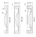
- FIGS. 3-4 are cross sectional side views of a lens assembly of a plurality of stacked multi-layered lenses.
- FIG. 5 is a cross sectional side view of the lens assembly (of a plurality of stacked multi-layered lenses) mounted on an image sensor assembly.
- the present invention is a multi-layer lens, and the method of manufacturing the same.
- the number of layers, and the composition of each layer, can be varied to achieve the desired optical properties of the lens.
- FIGS. 1A-1K illustrate the sequence of steps for manufacturing a multi-layer lens.
- the resulting lens will comprise three layers of material.
- the process begins by providing a smooth carrier 10 (e.g. Teflon), which is used as a lens carrier during the manufacturing process.
- carrier 10 can be round (6 to 12 inches in diameter), with sidewalls 12 extending up from its upper surface 14 to contain the lens materials on the upper surface 14 , as illustrated in FIG. 1A . While preferably a plurality of lenses are formed on carrier 10 simultaneously, for simplicity, the remaining figures illustrate the formation of a single lens on just a portion of carrier 10 .
- a first polymer layer 16 is formed on surface 10 .
- polymer formation is done by spray coating deposition, due to its even coating property.
- Polymer deposition is followed by a curing process.
- Polymer layer 16 can be epoxy silicone monomer, cycloaliphatic epoxy compounds, UV curable polymers, acrylate polymer, PMMA, COP, PC, ORNOCOMP or any other well-known optical polymer with desirable optical properties.
- a photo-resist layer 18 is formed over polymer layer 16 , for example, by spray coating, spin coating or any other photo-resist deposition process (which are known in the art).
- the photo-resist layer is then patterned using a photo-lithography exposure and development process (which are all well known in the art), leaving portions of the polymer layer 16 exposed.
- FIG. 1B The resulting structure is shown in FIG. 1B .
- An isotropic etch process is next performed to selectively etch the exposed portions of polymer layer 16 .
- a wet isotropic etching process involving a wet bath of etch agent for the polymer of layer 16 can be used, which dissolves unprotected portions of layer 16 to create cavity 20 formed into the upper surface of layer 16 in the form of a ring around the optical area), as illustrated in FIG. 1C .
- the curvature of cavity 20 can be controlled by the pattern of photo-resist 18 and the etching solution used.
- photo-resist 18 is removed, the cavity 20 is filled with photo-resist 22 .
- a second polymer layer 24 is then formed over polymer layer 16 (and photo-resist 22 ).
- Polymer layer 24 can be formed with the same material(s) or different material(s) (and same or different thickness) as polymer layer 16 , depending upon the desired optical properties provided by itself and/or in combination of the other polymer layers.
- a photo-resist layer 26 is then formed over polymer layer 24 , and patterned to expose portions of polymer layer 24 (in this example those portions disposed over photo-resist 22 ), as illustrated in FIG. 1D . Photo-resist 26 is different from (i.e. etch selective relative to) photo-resist 22 .
- An isotropic etch process is next performed to selectively etch the exposed portions of polymer layer 24 .
- a wet isotropic etching process involving a wet bath of etch agent for the polymer of layer 24 can be used, which dissolves unprotected portions of layer 24 such that cavity 20 extends up through layer 24 , as illustrated in FIG. 1E .
- the curvature and angle of the walls of cavity 20 as they extend through layer 24 can be controlled by the thickness of polymer layer 24 , the pattern of photo-resist 26 and the etching solution used.
- Photo-resist 26 is removed, the cavity 20 (as expanded through layer 24 ) is filled with photo-resist 22 .
- a third polymer layer 28 is then formed over polymer layer 24 (and photo-resist 22 ).
- Polymer layer 28 can be formed with the same material(s) or different material(s) (and same or different thickness) as polymer layers 16 and/or 24 , depending upon the desired optical properties provided by itself and/or in combination of the other polymer layers.
- a photo-resist layer 30 is then formed over polymer layer 28 , and patterned to expose portions of polymer layer 28 that are disposed over photo-resist 22 , as illustrated in FIG. 1F . Photo-resist 30 is different from (i.e. etch selective relative to) photo-resist 22 .
- An isotropic etch process is next performed to selectively etch the exposed portions of polymer layer 28 .
- a wet isotropic etching process involving a wet bath of etch agent for the polymer of layer 28 can be used, which dissolves unprotected portions of layer 28 (i.e. leaving cavity 20 extending up through layer 28 ).
- the curvature and angle of the walls of cavity 20 as they extend through layer 28 can be controlled by the thickness of polymer layer 28 , the pattern of photo-resist 30 and the etching solution used. Photo-resist 30 and 22 are then removed, leaving the structure illustrated in FIG. 1G .
- cavity 20 is no longer in the shape of a ring, but is now circular with a non-planar cavity surface 20 a that extends through (i.e. is defined by) all three polymer layers 16 , 24 and 28 .
- the cavity surface 20 a defines the lens surface as further explained below.
- a soft isotropic etch can be performed to smooth out any roughness on the cavity surface 20 a , as well as any steps or gaps between polymer layers 16 / 24 / 28 along the cavity surface 20 a .
- a similar optional surface polishing may be performed on the lens backside (i.e. the bottom surface of polymer layer 16 abutting carrier 10 after removal from the carrier 10 ).
- Surface 20 a can be optionally coated with an IR coating, which can include Copper (Cu), Gold, Hafnium Oxide (HfO2), ITO (Indium Tin Oxide), Magnesium Oxide (MgO), Nickel (Ni), Silicon Monoxide (SiO), Silver, Titanium Dioxide (TiO2), Tantalum Oxide (Ta2O5), Zirconium Oxideany and/or any other appropriate IR coating material.
- the IR coating can be applied using standard deposition techniques which are well known in the art.
- the back surface i.e. bottom surface of polymer layer 16 abutting the carrier 10
- an AR coating after removal from the carrier 10 ) using antireflection materials that are well known in the art.
- Alignment marks are then formed on or in the top surface of polymer layer 28 . If the alignment marks 32 are formed on the polymer layer 28 top surface (as shown in FIG. 1H ), they can be formed with a polymer, an epoxy, a resin, a metal, etc. as a protrusion that preferably extends from the polymer layer 28 top surface with a height of at least 3 ⁇ m. If the alignment marks 32 are formed into the polymer layer 28 top surface (as shown in FIG. 1I ), they can be formed as a cavity or trench using a laser preferably having a depth of at least 3 ⁇ m. Alignment marks can have any desired shape, such as for example circular, rectangular, cross shaped, T-shaped, etc. Alignment marks 32 can additionally or alternately be formed on or in the bottom surface of polymer layer 16 .
- the carrier 10 is then removed, and the structure is then diced along dicing lines 34 as illustrated in FIG. 1J to separate each individual lenses 36 .
- the final lens 36 is illustrated in FIG. 1K .
- Lens 36 is a substrate formed of discrete layers of polymer material.
- Lens 36 includes a lens surface 20 a having a very specific shape in order to produce the desired optical focusing for light passing through lens 36 .
- the shape of lens surface 20 a can be consistently and precisely controlled using the polymer deposition, photo-lithography and etch processes described above. By varying the compositions of the three layers 16 , 24 and 28 relative to each other, as well as optionally continuing to add additional discrete layers to the three described above in a similar manner, more complex and diverse optical focusing performance can be achieved.
- FIGS. 2A-2N illustrate the sequence of steps for manufacturing an alternate embodiment multi-layer lens.
- the process begins with the structure of FIG. 1B , except for the relative locations of the exposed portions of polymer layer 16 , as illustrated in FIG. 2A .
- An anisotropic etch is then performed to selectively etch the exposed portions of polymer layer 16 .
- a plasma or wet anisotropic etching process removes portions of layer 16 to form an annular trench-shaped cavity 40 into the upper surface of layer 16 (i.e. in the form of a ring around the optical area).
- the photo-resist 18 is then removed, leaving the structure illustrated in FIG. 2B .
- a photo-resist layer 42 is deposited over the structure (including inside cavity 40 ).
- a photolithography process is used to remove selective portions of photo-resist layer 42 (along the inner sidewall of cavity 40 , and that portion on the upper surface of polymer layer 16 that is adjacent the inner sidewall of cavity 40 ), as illustrated in FIG. 2C .
- An isotropic etching process such as a wet bath of polymer etch agent, is used to dissolve exposed portions of polymer layer 16 , creating a curved shaped to the inner-sidewall 40 a of cavity 40 .
- the resulting structure is illustrated in FIG. 2D (after photo-resist 42 is removed).
- the curvature and angle of the inner-sidewall 40 a of cavity 40 can be controlled by the thickness of polymer layer 16 , the pattern of photo-resist 42 and the etch material.
- a second polymer layer 44 is next formed over polymer layer 16 (filling cavity 40 ).
- Polymer layer 44 can be formed with the same material(s) or different material(s) (and same or different thickness) as polymer layer 16 , depending upon the desired optical properties provided by itself and/or in combination of the other polymer layers.
- a photo-resist layer 46 is then formed over polymer layer 44 , and patterned to expose portions of polymer layer 44 , as illustrated in FIG. 2E .
- An anisotropic etch is then performed to selectively etch the exposed portions of polymer layer 44 .
- a plasma or wet anisotropic etching process removes portions of layer 44 to form an annular trench-shaped cavity 48 into the upper surface of layer 44 (i.e. in the form of a ring around the optical area).
- a photo-resist layer 50 is deposited over the structure (including inside cavity 48 ).
- a photolithography process is used to remove selective portions of photo-resist layer 50 (along the inner sidewall of cavity 48 , and that portion on the upper surface of polymer layer 44 that is adjacent the inner sidewall of cavity 48 ), as illustrated in FIG. 2F .
- An isotropic etching process such as a wet bath of polymer etch agent, is used to dissolve exposed portions of polymer layer 44 , creating a curved inner-sidewall 48 a to cavity 48 .
- the resulting structure is illustrated in FIG. 2G (after photo-resist 50 is removed).
- the curvature and angle of inner-sidewall 48 a of cavity 48 can be controlled by the thickness of polymer layer 44 , the pattern of photo-resist 50 , and the etch material.
- a third polymer layer 52 is next formed over polymer layer 44 (filling cavity 48 ).
- Polymer layer 52 can be formed with the same material(s) or different material(s) (and same or different thicknesses) as polymer layers 16 and 44 , depending upon the desired optical properties provided by itself and/or in combination of the other polymer layers.
- a photo-resist layer 54 is then formed over polymer layer 52 , and patterned to expose portions of polymer layer 52 , as illustrated in FIG. 2H .
- An anisotropic etch is then performed to selectively etch the exposed portions of polymer layer 52 .
- a plasma or wet anisotropic etching process removes portions of layer 52 to form an annular trench-shaped cavity 56 into the upper surface of layer 44 (i.e. in the form of a ring around the optical area).
- a photo-resist layer 58 is deposited over the structure (including inside cavity 56 ).
- a photolithography process is used to remove selective portions of photo-resist layer 56 (along the inner sidewall of cavity 56 , and that portion on the upper surface of polymer layer 52 that is adjacent the inner sidewall of cavity 56 ), as illustrated in FIG. 2I .
- An isotropic etching process such as a wet bath of polymer etch agent, is used to dissolve exposed portions of polymer layer 52 , creating a curved inner-sidewall 56 a to cavity 56 .
- the resulting structure is illustrated in FIG. 2J (after photo-resist 58 is removed).
- the curvature and angle of the inner-sidewall 56 a of cavity 56 can be controlled by the thickness of polymer layer 52 , the pattern of photo-resist 58 , and the etch material.
- Surface 56 a defines the lens surface.
- a soft isotropic etch can be performed to smooth out any roughness on surface 56 a , as well as any steps or gaps between polymer layers 16 / 44 / 52 .
- a similar surface polishing may be (i.e. optional) performed on the lens backside (i.e. the bottom surface of polymer layer 16 abutting carrier 10 after removal from the carrier 10 ).
- Alignment marks 32 can be formed on or in the top surface of polymer layer 52 as described above, and shown in FIGS. 2K and 2L . Alignment marks 32 could additionally or alternately be formed on or in the bottom surface of polymer layer 16 .
- lens 60 is a substrate formed of discrete layers of polymer material. Not only can non-planar lens surface 56 a be precisely shaped and formed to provide the desired focusing effects, but the abutting non-planar surfaces of discretely formed layers 16 and 44 , and the abutting non-planar surfaces of discretely formed layers 44 and 52 , can provide additional light focusing effects when the layers 16 , 44 and/or 52 are formed of different materials with different light propagating properties (e.g. different effective indices of refraction).
- Lens assemblies can be formed by stacking a plurality of lenses of similar or dissimilar design to achieve the light focusing performance required for the particular application.
- FIG. 3 illustrates five lenses 62 a - 62 e stacked together using bonding material 64 to form a lens assembly 66 .
- the number of lenses 62 and lens shapes can vary depending upon the performance requirements of the design.
- Bonding material 64 can be a polymer, epoxy based, a resin, a metal or any other appropriate bonding material.
- epoxy based adhesive 64 is applied to the non-alignment mark side of lenses 62 a - 62 e .
- a stacking tool with an alignment camera can be used to align the alignment marks 32 before bonding the lenses 62 a - 62 e together.
- a light shielding layer 68 is deposited on the lens stack sidewalls (i.e. extending around and between the outer edges of the lenses), as illustrated in FIG. 4 (i.e. for lenses having a round outer edge, layer 68 would be in the form of a cylinder).
- Light shielding layer 68 can be polymer, epoxy based, resin, paint, tape, metal, plastic/metallic enclosure or any other non-transparent material(s).
- light shielding layer 68 is at least 5 ⁇ m in thickness and made of polymer based material such as black solder mask.
- FIG. 5 illustrates the lens assembly 66 bonded to a CMOS image sensor assembly 70 via bond joints 71 .
- Bond joints 71 can be a polymer, epoxy based, resin, metallic or any other bonding material.
- bond joints 71 are an epoxy based adhesive that is deposited on the bottom side of lens module 66 , where the lens module 66 is then picked up and placed on the CMOS image sensor assembly 70 for bonding.
- Image sensor assembly 70 generally includes photo detectors 72 , circuitry 74 , color filters 76 , microlenses 78 , contact pads 80 , wires 82 , contact pads 84 and a circuit board 86 .
- a more detailed discussion of image sensor assembly 70 can be found in co-pending U.S. patent application Ser. No. 13/343,682, which is incorporated herein by reference for all purposes.
- lens 36 / 60 are shown and described with three polymer layers, they can contain N polymer layers, where N is any integer 2 or greater.
- references to the present invention herein are not intended to limit the scope of any claim or claim term, but instead merely make reference to one or more features that may be covered by one or more of the claims. Materials, processes and numerical examples described above are exemplary only, and should not be deemed to limit the claims.
- the term “adjacent” includes “directly adjacent” (no intermediate materials, elements or space disposed therebetween) and “indirectly adjacent” (intermediate materials, elements or space disposed there between), “mounted to” includes “directly mounted to” (no intermediate materials, elements or space disposed there between) and “indirectly mounted to” (intermediate materials, elements or spaced disposed there between), and “electrically coupled” includes “directly electrically coupled to” (no intermediate materials or elements there between that electrically connect the elements together) and “indirectly electrically coupled to” (intermediate materials or elements there between that electrically connect the elements together).
- forming an element “over a substrate” can include forming the element directly on the substrate with no intermediate materials/elements therebetween, as well as forming the element indirectly on the substrate with one or more intermediate materials/elements therebetween.
Abstract
Description
Claims (32)
Priority Applications (4)
| Application Number | Priority Date | Filing Date | Title |
|---|---|---|---|
| US13/356,328 US8570669B2 (en) | 2012-01-23 | 2012-01-23 | Multi-layer polymer lens and method of making same |
| CN201210043599.8A CN103219343B (en) | 2012-01-23 | 2012-02-24 | Multiple layer polymer lens and manufacture method thereof |
| TW101142826A TWI501864B (en) | 2012-01-23 | 2012-11-16 | Multi-layer polymer lens and method of making same |
| KR1020130006551A KR101445022B1 (en) | 2012-01-23 | 2013-01-21 | Multi-layer polymer lens, method of making same and lens assembly |
Applications Claiming Priority (1)
| Application Number | Priority Date | Filing Date | Title |
|---|---|---|---|
| US13/356,328 US8570669B2 (en) | 2012-01-23 | 2012-01-23 | Multi-layer polymer lens and method of making same |
Publications (2)
| Publication Number | Publication Date |
|---|---|
| US20130188267A1 US20130188267A1 (en) | 2013-07-25 |
| US8570669B2 true US8570669B2 (en) | 2013-10-29 |
Family
ID=48797004
Family Applications (1)
| Application Number | Title | Priority Date | Filing Date |
|---|---|---|---|
| US13/356,328 Active 2032-05-27 US8570669B2 (en) | 2012-01-23 | 2012-01-23 | Multi-layer polymer lens and method of making same |
Country Status (4)
| Country | Link |
|---|---|
| US (1) | US8570669B2 (en) |
| KR (1) | KR101445022B1 (en) |
| CN (1) | CN103219343B (en) |
| TW (1) | TWI501864B (en) |
Cited By (6)
| Publication number | Priority date | Publication date | Assignee | Title |
|---|---|---|---|---|
| US9853079B2 (en) | 2015-02-24 | 2017-12-26 | Optiz, Inc. | Method of forming a stress released image sensor package structure |
| US9893213B2 (en) | 2014-08-18 | 2018-02-13 | Optiz, Inc. | Method of forming a wire bond sensor package |
| US9893218B2 (en) | 2013-12-05 | 2018-02-13 | Optiz, Inc. | Sensor package with cooling feature |
| US9996725B2 (en) | 2016-11-03 | 2018-06-12 | Optiz, Inc. | Under screen sensor assembly |
| US10741613B2 (en) * | 2014-10-14 | 2020-08-11 | Ams Sensors Singapore Pte. Ltd. | Optical element stack assemblies |
| US11408589B2 (en) | 2019-12-05 | 2022-08-09 | Optiz, Inc. | Monolithic multi-focus light source device |
Families Citing this family (7)
| Publication number | Priority date | Publication date | Assignee | Title |
|---|---|---|---|---|
| US9496247B2 (en) * | 2013-08-26 | 2016-11-15 | Optiz, Inc. | Integrated camera module and method of making same |
| CN103486536A (en) * | 2013-09-09 | 2014-01-01 | 苏州金科信汇光电科技有限公司 | Combined-type lens and manufacturing method thereof |
| US9461190B2 (en) | 2013-09-24 | 2016-10-04 | Optiz, Inc. | Low profile sensor package with cooling feature and method of making same |
| TWI600125B (en) * | 2015-05-01 | 2017-09-21 | 精材科技股份有限公司 | Chip package and manufacturing method thereof |
| CN108700721B (en) * | 2015-11-12 | 2021-12-31 | 赫普塔冈微光有限公司 | Optical element stack assembly |
| JP7449042B2 (en) * | 2019-02-28 | 2024-03-13 | 日本ルメンタム株式会社 | Photoelectric conversion element, optical subassembly, and method for manufacturing photoelectric conversion element |
| CN111048542B (en) * | 2019-12-25 | 2023-09-05 | 上海集成电路研发中心有限公司 | Manufacturing method of inner lens |
Citations (32)
| Publication number | Priority date | Publication date | Assignee | Title |
|---|---|---|---|---|
| US6777767B2 (en) | 1999-12-10 | 2004-08-17 | Shellcase Ltd. | Methods for producing packaged integrated circuit devices & packaged integrated circuit devices produced thereby |
| US20040251525A1 (en) | 2003-06-16 | 2004-12-16 | Shellcase Ltd. | Methods and apparatus for packaging integrated circuit devices |
| US20050104179A1 (en) | 2003-07-03 | 2005-05-19 | Shellcase Ltd. | Methods and apparatus for packaging integrated circuit devices |
| US7033664B2 (en) | 2002-10-22 | 2006-04-25 | Tessera Technologies Hungary Kft | Methods for producing packaged integrated circuit devices and packaged integrated circuit devices produced thereby |
| US7157742B2 (en) | 1998-02-06 | 2007-01-02 | Tessera Technologies Hungary Kft. | Integrated circuit device |
| US20070190691A1 (en) | 2006-01-23 | 2007-08-16 | Tessera Technologies Hungary Kft. | Wafer level chip packaging |
| US20070190747A1 (en) | 2006-01-23 | 2007-08-16 | Tessera Technologies Hungary Kft. | Wafer level packaging to lidded chips |
| US20080083977A1 (en) | 2006-10-10 | 2008-04-10 | Tessera, Inc. | Edge connect wafer level stacking |
| US20080083976A1 (en) | 2006-10-10 | 2008-04-10 | Tessera, Inc. | Edge connect wafer level stacking |
| US20080099907A1 (en) | 2006-10-31 | 2008-05-01 | Tessera Technologies Hungary Kft. | Wafer-level fabrication of lidded chips with electrodeposited dielectric coating |
| US20080099900A1 (en) | 2006-10-31 | 2008-05-01 | Tessera Technologies Hungary Kft. | Wafer-level fabrication of lidded chips with electrodeposited dielectric coating |
| US20080116544A1 (en) | 2006-11-22 | 2008-05-22 | Tessera, Inc. | Packaged semiconductor chips with array |
| US20080116545A1 (en) | 2006-11-22 | 2008-05-22 | Tessera, Inc. | Packaged semiconductor chips |
| US20080150121A1 (en) | 2006-12-20 | 2008-06-26 | Tessera Technologies Hungary Kft. | Microelectronic assemblies having compliancy and methods therefor |
| US20080246136A1 (en) | 2007-03-05 | 2008-10-09 | Tessera, Inc. | Chips having rear contacts connected by through vias to front contacts |
| US20090115047A1 (en) | 2007-10-10 | 2009-05-07 | Tessera, Inc. | Robust multi-layer wiring elements and assemblies with embedded microelectronic elements |
| US20090160065A1 (en) | 2006-10-10 | 2009-06-25 | Tessera, Inc. | Reconstituted Wafer Level Stacking |
| US20090212381A1 (en) | 2008-02-26 | 2009-08-27 | Tessera, Inc. | Wafer level packages for rear-face illuminated solid state image sensors |
| US20100053407A1 (en) | 2008-02-26 | 2010-03-04 | Tessera, Inc. | Wafer level compliant packages for rear-face illuminated solid state image sensors |
| US20100237452A1 (en) | 2009-03-18 | 2010-09-23 | Kenichiro Hagiwara | Semiconductor device and backside illumination solid-state imaging device |
| US7859033B2 (en) | 2008-07-09 | 2010-12-28 | Eastman Kodak Company | Wafer level processing for backside illuminated sensors |
| US20120018868A1 (en) | 2010-07-23 | 2012-01-26 | Tessera Research Llc | Microelectronic elements having metallic pads overlying vias |
| US20120018863A1 (en) | 2010-07-23 | 2012-01-26 | Tessera Research Llc | Microelectronic elements with rear contacts connected with via first or via middle structures |
| US20120018894A1 (en) | 2010-07-23 | 2012-01-26 | Tessera Research Llc | Non-lithographic formation of three-dimensional conductive elements |
| US20120018893A1 (en) | 2010-07-23 | 2012-01-26 | Tessera Research Llc | Methods of forming semiconductor elements using micro-abrasive particle stream |
| US20120018895A1 (en) | 2010-07-23 | 2012-01-26 | Tessera Research Llc | Active chip on carrier or laminated chip having microelectronic element embedded therein |
| US20120020026A1 (en) | 2010-07-23 | 2012-01-26 | Tessera Research Llc | Microelectronic elements with post-assembly planarization |
| US20120068327A1 (en) | 2010-09-17 | 2012-03-22 | Tessera Research Llc | Multi-function and shielded 3d interconnects |
| US20120068330A1 (en) | 2010-09-17 | 2012-03-22 | Tessera Research Llc | Staged via formation from both sides of chip |
| US20120068352A1 (en) | 2010-09-16 | 2012-03-22 | Tessera Research Llc | Stacked chip assembly having vertical vias |
| US20120068351A1 (en) | 2010-09-16 | 2012-03-22 | Tessera Research Llc | Chip assembly having via interconnects joined by plating |
| US20120182623A1 (en) * | 2009-12-21 | 2012-07-19 | Frank Wippermann | Method for Manufacturing a Structure, Optical Component, Optical Layer Stack |
Family Cites Families (6)
| Publication number | Priority date | Publication date | Assignee | Title |
|---|---|---|---|---|
| JP2007503609A (en) * | 2003-08-23 | 2007-02-22 | コーニンクレッカ フィリップス エレクトロニクス エヌ ヴィ | Color display device manufacturing method and color display device |
| KR100652379B1 (en) * | 2004-09-11 | 2006-12-01 | 삼성전자주식회사 | CMOS image sensor and manufacturing method thereof |
| US7029944B1 (en) * | 2004-09-30 | 2006-04-18 | Sharp Laboratories Of America, Inc. | Methods of forming a microlens array over a substrate employing a CMP stop |
| JP4510613B2 (en) * | 2004-12-28 | 2010-07-28 | パナソニック株式会社 | Method for manufacturing solid-state imaging device |
| NO326372B1 (en) * | 2006-09-21 | 2008-11-17 | Polight As | Polymer Lens |
| JP4891214B2 (en) * | 2007-12-13 | 2012-03-07 | シャープ株式会社 | Electronic element wafer module, electronic element module, sensor wafer module, sensor module, lens array plate, sensor module manufacturing method, and electronic information device |
-
2012
- 2012-01-23 US US13/356,328 patent/US8570669B2/en active Active
- 2012-02-24 CN CN201210043599.8A patent/CN103219343B/en active Active
- 2012-11-16 TW TW101142826A patent/TWI501864B/en active
-
2013
- 2013-01-21 KR KR1020130006551A patent/KR101445022B1/en active IP Right Grant
Patent Citations (48)
| Publication number | Priority date | Publication date | Assignee | Title |
|---|---|---|---|---|
| US7157742B2 (en) | 1998-02-06 | 2007-01-02 | Tessera Technologies Hungary Kft. | Integrated circuit device |
| US6777767B2 (en) | 1999-12-10 | 2004-08-17 | Shellcase Ltd. | Methods for producing packaged integrated circuit devices & packaged integrated circuit devices produced thereby |
| US7033664B2 (en) | 2002-10-22 | 2006-04-25 | Tessera Technologies Hungary Kft | Methods for producing packaged integrated circuit devices and packaged integrated circuit devices produced thereby |
| US20080012115A1 (en) | 2003-06-16 | 2008-01-17 | Tessera Technologies Hungary Kft. | Methods and apparatus for packaging integrated circuit devices |
| US6972480B2 (en) | 2003-06-16 | 2005-12-06 | Shellcase Ltd. | Methods and apparatus for packaging integrated circuit devices |
| US20050205977A1 (en) | 2003-06-16 | 2005-09-22 | Shellcase Ltd. | Methods and apparatus for packaging integrated circuit devices |
| US7265440B2 (en) | 2003-06-16 | 2007-09-04 | Tessera Technologies Hungary Kft. | Methods and apparatus for packaging integrated circuit devices |
| US7642629B2 (en) | 2003-06-16 | 2010-01-05 | Tessera Technologies Hungary Kft. | Methods and apparatus for packaging integrated circuit devices |
| US20040251525A1 (en) | 2003-06-16 | 2004-12-16 | Shellcase Ltd. | Methods and apparatus for packaging integrated circuit devices |
| US20050104179A1 (en) | 2003-07-03 | 2005-05-19 | Shellcase Ltd. | Methods and apparatus for packaging integrated circuit devices |
| US7192796B2 (en) | 2003-07-03 | 2007-03-20 | Tessera Technologies Hungary Kft. | Methods and apparatus for packaging integrated circuit devices |
| US20070138498A1 (en) | 2003-07-03 | 2007-06-21 | Tessera Technologies Hungary Kft. | Methods and apparatus for packaging integrated circuit devices |
| US7495341B2 (en) | 2003-07-03 | 2009-02-24 | Tessera Technologies Hungary Kft. | Methods and apparatus for packaging integrated circuit devices |
| US20080017879A1 (en) | 2003-07-03 | 2008-01-24 | Tessera Technologies Hungary Kft. | Methods and apparatus for packaging integrated circuit devices |
| US20070190691A1 (en) | 2006-01-23 | 2007-08-16 | Tessera Technologies Hungary Kft. | Wafer level chip packaging |
| US20070190747A1 (en) | 2006-01-23 | 2007-08-16 | Tessera Technologies Hungary Kft. | Wafer level packaging to lidded chips |
| US20090160065A1 (en) | 2006-10-10 | 2009-06-25 | Tessera, Inc. | Reconstituted Wafer Level Stacking |
| US20080083977A1 (en) | 2006-10-10 | 2008-04-10 | Tessera, Inc. | Edge connect wafer level stacking |
| US20110187007A1 (en) | 2006-10-10 | 2011-08-04 | Tessera, Inc. | Edge connect wafer level stacking |
| US20110031629A1 (en) | 2006-10-10 | 2011-02-10 | Tessera, Inc. | Edge connect wafer level stacking |
| US20080083976A1 (en) | 2006-10-10 | 2008-04-10 | Tessera, Inc. | Edge connect wafer level stacking |
| US20110049696A1 (en) | 2006-10-10 | 2011-03-03 | Tessera, Inc. | Off-chip vias in stacked chips |
| US20110033979A1 (en) | 2006-10-10 | 2011-02-10 | Tessera, Inc. | Edge connect wafer level stacking |
| US20080099907A1 (en) | 2006-10-31 | 2008-05-01 | Tessera Technologies Hungary Kft. | Wafer-level fabrication of lidded chips with electrodeposited dielectric coating |
| US20080099900A1 (en) | 2006-10-31 | 2008-05-01 | Tessera Technologies Hungary Kft. | Wafer-level fabrication of lidded chips with electrodeposited dielectric coating |
| US20080116545A1 (en) | 2006-11-22 | 2008-05-22 | Tessera, Inc. | Packaged semiconductor chips |
| US20080116544A1 (en) | 2006-11-22 | 2008-05-22 | Tessera, Inc. | Packaged semiconductor chips with array |
| US20110012259A1 (en) | 2006-11-22 | 2011-01-20 | Tessera, Inc. | Packaged semiconductor chips |
| US20080150121A1 (en) | 2006-12-20 | 2008-06-26 | Tessera Technologies Hungary Kft. | Microelectronic assemblies having compliancy and methods therefor |
| US20100230812A1 (en) | 2006-12-20 | 2010-09-16 | Tessera, Inc. | Microelectronic Assemblies Having Compliancy and Methods Therefor |
| US20080246136A1 (en) | 2007-03-05 | 2008-10-09 | Tessera, Inc. | Chips having rear contacts connected by through vias to front contacts |
| US20100225006A1 (en) | 2007-03-05 | 2010-09-09 | Tessera, Inc. | Chips having rear contacts connected by through vias to front contacts |
| US20090115047A1 (en) | 2007-10-10 | 2009-05-07 | Tessera, Inc. | Robust multi-layer wiring elements and assemblies with embedded microelectronic elements |
| US20100053407A1 (en) | 2008-02-26 | 2010-03-04 | Tessera, Inc. | Wafer level compliant packages for rear-face illuminated solid state image sensors |
| US20090212381A1 (en) | 2008-02-26 | 2009-08-27 | Tessera, Inc. | Wafer level packages for rear-face illuminated solid state image sensors |
| US7859033B2 (en) | 2008-07-09 | 2010-12-28 | Eastman Kodak Company | Wafer level processing for backside illuminated sensors |
| US20100237452A1 (en) | 2009-03-18 | 2010-09-23 | Kenichiro Hagiwara | Semiconductor device and backside illumination solid-state imaging device |
| US20120182623A1 (en) * | 2009-12-21 | 2012-07-19 | Frank Wippermann | Method for Manufacturing a Structure, Optical Component, Optical Layer Stack |
| US20120018868A1 (en) | 2010-07-23 | 2012-01-26 | Tessera Research Llc | Microelectronic elements having metallic pads overlying vias |
| US20120018863A1 (en) | 2010-07-23 | 2012-01-26 | Tessera Research Llc | Microelectronic elements with rear contacts connected with via first or via middle structures |
| US20120018894A1 (en) | 2010-07-23 | 2012-01-26 | Tessera Research Llc | Non-lithographic formation of three-dimensional conductive elements |
| US20120018893A1 (en) | 2010-07-23 | 2012-01-26 | Tessera Research Llc | Methods of forming semiconductor elements using micro-abrasive particle stream |
| US20120018895A1 (en) | 2010-07-23 | 2012-01-26 | Tessera Research Llc | Active chip on carrier or laminated chip having microelectronic element embedded therein |
| US20120020026A1 (en) | 2010-07-23 | 2012-01-26 | Tessera Research Llc | Microelectronic elements with post-assembly planarization |
| US20120068352A1 (en) | 2010-09-16 | 2012-03-22 | Tessera Research Llc | Stacked chip assembly having vertical vias |
| US20120068351A1 (en) | 2010-09-16 | 2012-03-22 | Tessera Research Llc | Chip assembly having via interconnects joined by plating |
| US20120068327A1 (en) | 2010-09-17 | 2012-03-22 | Tessera Research Llc | Multi-function and shielded 3d interconnects |
| US20120068330A1 (en) | 2010-09-17 | 2012-03-22 | Tessera Research Llc | Staged via formation from both sides of chip |
Non-Patent Citations (13)
| Title |
|---|
| U.S. Appl. No. 13/157,193, filed Jun. 9, 2011, Oganesian, Vage. |
| U.S. Appl. No. 13/157,202, filed Jun. 9, 2011, Oganesian, Vage. |
| U.S. Appl. No. 13/157,207, filed Jun. 9, 2011, Oganesian, Vage. |
| U.S. Appl. No. 13/186,357, filed Jul. 19, 2011, Oganesian, Vage. |
| U.S. Appl. No. 13/225,092, filed Sep. 2, 2011, Oganesian, Vage. |
| U.S. Appl. No. 13/301,683, filed Nov. 21, 2011, Oganesian, Vage. |
| U.S. Appl. No. 13/312,826, filed Dec. 6, 2011, Oganesian, Vage. |
| U.S. Appl. No. 13/343,682, filed Jan. 4, 2012, Oganesian, Vage. |
| U.S. Appl. No. 13/423,045, filed Mar. 16, 2012, Oganesian, Vage. |
| U.S. Appl. No. 13/427,604, filed Mar. 22, 2012, Oganesian, Vage. |
| U.S. Appl. No. 13/468,632, filed May 10, 2012, Oganesian, Vage. |
| U.S. Appl. No. 13/559,510, filed Jul. 26, 2012, Oganesian, Vage. |
| U.S. Appl. No. 13/609,002, filed Sep. 10, 2012, Oganesian, Vage. |
Cited By (8)
| Publication number | Priority date | Publication date | Assignee | Title |
|---|---|---|---|---|
| US9893218B2 (en) | 2013-12-05 | 2018-02-13 | Optiz, Inc. | Sensor package with cooling feature |
| US9972730B2 (en) | 2013-12-05 | 2018-05-15 | Optiz, Inc. | Method of making a sensor package with cooling feature |
| US10199519B2 (en) | 2013-12-05 | 2019-02-05 | Optiz, Inc. | Method of making a sensor package with cooling feature |
| US9893213B2 (en) | 2014-08-18 | 2018-02-13 | Optiz, Inc. | Method of forming a wire bond sensor package |
| US10741613B2 (en) * | 2014-10-14 | 2020-08-11 | Ams Sensors Singapore Pte. Ltd. | Optical element stack assemblies |
| US9853079B2 (en) | 2015-02-24 | 2017-12-26 | Optiz, Inc. | Method of forming a stress released image sensor package structure |
| US9996725B2 (en) | 2016-11-03 | 2018-06-12 | Optiz, Inc. | Under screen sensor assembly |
| US11408589B2 (en) | 2019-12-05 | 2022-08-09 | Optiz, Inc. | Monolithic multi-focus light source device |
Also Published As
| Publication number | Publication date |
|---|---|
| TW201332754A (en) | 2013-08-16 |
| CN103219343B (en) | 2016-04-27 |
| KR101445022B1 (en) | 2014-09-26 |
| KR20130086175A (en) | 2013-07-31 |
| US20130188267A1 (en) | 2013-07-25 |
| TWI501864B (en) | 2015-10-01 |
| CN103219343A (en) | 2013-07-24 |
Similar Documents
| Publication | Publication Date | Title |
|---|---|---|
| US8570669B2 (en) | Multi-layer polymer lens and method of making same | |
| US9029759B2 (en) | Compact camera modules with features for reducing Z-height and facilitating lens alignment and methods for manufacturing the same | |
| EP3007228B1 (en) | Monolithic integration of plenoptic lenses on photosensor substrates | |
| US8675118B2 (en) | Image sensor | |
| US9634051B2 (en) | Optical devices, in particular computational cameras, and methods for manufacturing the same | |
| US20090321861A1 (en) | Microelectronic imagers with stacked lens assemblies and processes for wafer-level packaging of microelectronic imagers | |
| US9502461B2 (en) | Methods of fabricating camera module and spacer of a lens structure in the camera module | |
| WO2017090437A1 (en) | Camera module and electronic device | |
| JP6619174B2 (en) | Manufacturing apparatus and method | |
| JP2010118397A (en) | Camera module and process of manufacturing the same | |
| US20110292271A1 (en) | Camera module and fabrication method thereof | |
| US20070292127A1 (en) | Small form factor camera module with lens barrel and image sensor | |
| JP6670565B2 (en) | Manufacturing method and mold for laminated lens structure | |
| US10236314B2 (en) | Optical devices and opto-electronic modules and methods for manufacturing the same | |
| JP6660115B2 (en) | Substrate with lens and method of manufacturing laminated lens structure | |
| TWI625541B (en) | Trenched-substrate based lens manufacturing methods, and associated lens systems | |
| TWI594021B (en) | Wafer level optical elements and applications thereof | |
| Matthias et al. | CMOS image sensor wafer-level packaging | |
| US20070230948A1 (en) | Lens structure for an imaging device and method making same | |
| US10069018B1 (en) | Camera assembly with embedded components and redistribution layer interconnects | |
| KR101003636B1 (en) | Wafer lens and manufacturing method thereof and camera module having the wafer lens |
Legal Events
| Date | Code | Title | Description |
|---|---|---|---|
| AS | Assignment |
Owner name: CHINA WLCSP US, INC., CALIFORNIA Free format text: ASSIGNMENT OF ASSIGNORS INTEREST;ASSIGNOR:OGANESIAN, VAGE;REEL/FRAME:027975/0104 Effective date: 20120319 |
|
| AS | Assignment |
Owner name: OPTIZ, INC., CALIFORNIA Free format text: CHANGE OF NAME;ASSIGNOR:CHINA WLCSP US, INC.;REEL/FRAME:028406/0571 Effective date: 20120330 |
|
| STCF | Information on status: patent grant |
Free format text: PATENTED CASE |
|
| SULP | Surcharge for late payment | ||
| FEPP | Fee payment procedure |
Free format text: PAT HOLDER NO LONGER CLAIMS SMALL ENTITY STATUS, ENTITY STATUS SET TO UNDISCOUNTED (ORIGINAL EVENT CODE: STOL); ENTITY STATUS OF PATENT OWNER: LARGE ENTITY |
|
| FPAY | Fee payment |
Year of fee payment: 4 |
|
| MAFP | Maintenance fee payment |
Free format text: PAYMENT OF MAINTENANCE FEE, 8TH YEAR, LARGE ENTITY (ORIGINAL EVENT CODE: M1552); ENTITY STATUS OF PATENT OWNER: LARGE ENTITY Year of fee payment: 8 |