US8507924B2 - Light emitting diode with high aspect ratio submicron roughness for light extraction and methods of forming - Google Patents
Light emitting diode with high aspect ratio submicron roughness for light extraction and methods of forming Download PDFInfo
- Publication number
- US8507924B2 US8507924B2 US13/045,246 US201113045246A US8507924B2 US 8507924 B2 US8507924 B2 US 8507924B2 US 201113045246 A US201113045246 A US 201113045246A US 8507924 B2 US8507924 B2 US 8507924B2
- Authority
- US
- United States
- Prior art keywords
- light emitting
- submicron
- emitting diode
- mask
- template
- Prior art date
- Legal status (The legal status is an assumption and is not a legal conclusion. Google has not performed a legal analysis and makes no representation as to the accuracy of the status listed.)
- Active
Links
Images


Classifications
-
- H—ELECTRICITY
- H01—ELECTRIC ELEMENTS
- H01L—SEMICONDUCTOR DEVICES NOT COVERED BY CLASS H10
- H01L33/00—Semiconductor devices with at least one potential-jump barrier or surface barrier specially adapted for light emission; Processes or apparatus specially adapted for the manufacture or treatment thereof or of parts thereof; Details thereof
- H01L33/02—Semiconductor devices with at least one potential-jump barrier or surface barrier specially adapted for light emission; Processes or apparatus specially adapted for the manufacture or treatment thereof or of parts thereof; Details thereof characterised by the semiconductor bodies
- H01L33/20—Semiconductor devices with at least one potential-jump barrier or surface barrier specially adapted for light emission; Processes or apparatus specially adapted for the manufacture or treatment thereof or of parts thereof; Details thereof characterised by the semiconductor bodies with a particular shape, e.g. curved or truncated substrate
- H01L33/22—Roughened surfaces, e.g. at the interface between epitaxial layers
-
- H—ELECTRICITY
- H01—ELECTRIC ELEMENTS
- H01L—SEMICONDUCTOR DEVICES NOT COVERED BY CLASS H10
- H01L2224/00—Indexing scheme for arrangements for connecting or disconnecting semiconductor or solid-state bodies and methods related thereto as covered by H01L24/00
- H01L2224/01—Means for bonding being attached to, or being formed on, the surface to be connected, e.g. chip-to-package, die-attach, "first-level" interconnects; Manufacturing methods related thereto
- H01L2224/10—Bump connectors; Manufacturing methods related thereto
- H01L2224/12—Structure, shape, material or disposition of the bump connectors prior to the connecting process
- H01L2224/13—Structure, shape, material or disposition of the bump connectors prior to the connecting process of an individual bump connector
-
- H—ELECTRICITY
- H01—ELECTRIC ELEMENTS
- H01L—SEMICONDUCTOR DEVICES NOT COVERED BY CLASS H10
- H01L2924/00—Indexing scheme for arrangements or methods for connecting or disconnecting semiconductor or solid-state bodies as covered by H01L24/00
- H01L2924/0001—Technical content checked by a classifier
- H01L2924/00011—Not relevant to the scope of the group, the symbol of which is combined with the symbol of this group
-
- H—ELECTRICITY
- H01—ELECTRIC ELEMENTS
- H01L—SEMICONDUCTOR DEVICES NOT COVERED BY CLASS H10
- H01L2924/00—Indexing scheme for arrangements or methods for connecting or disconnecting semiconductor or solid-state bodies as covered by H01L24/00
- H01L2924/0001—Technical content checked by a classifier
- H01L2924/00014—Technical content checked by a classifier the subject-matter covered by the group, the symbol of which is combined with the symbol of this group, being disclosed without further technical details
-
- H—ELECTRICITY
- H01—ELECTRIC ELEMENTS
- H01L—SEMICONDUCTOR DEVICES NOT COVERED BY CLASS H10
- H01L2924/00—Indexing scheme for arrangements or methods for connecting or disconnecting semiconductor or solid-state bodies as covered by H01L24/00
- H01L2924/10—Details of semiconductor or other solid state devices to be connected
- H01L2924/1015—Shape
- H01L2924/10155—Shape being other than a cuboid
- H01L2924/10158—Shape being other than a cuboid at the passive surface
-
- H—ELECTRICITY
- H01—ELECTRIC ELEMENTS
- H01L—SEMICONDUCTOR DEVICES NOT COVERED BY CLASS H10
- H01L33/00—Semiconductor devices with at least one potential-jump barrier or surface barrier specially adapted for light emission; Processes or apparatus specially adapted for the manufacture or treatment thereof or of parts thereof; Details thereof
- H01L33/005—Processes
- H01L33/0095—Post-treatment of devices, e.g. annealing, recrystallisation or short-circuit elimination
Definitions
- This invention relates to light emitting diodes (LEDs) and more particularly to new surface morphologies for enhancing the extraction of light from LEDs and methods of manufacturing LEDs having such surfaces.
- LEDs Light emitting diodes
- LEDs are an important class of solid state devices that convert electric energy to light and generally comprise an active layer of semiconductor material sandwiched between two oppositely doped layers. When a bias is applied across the doped layers, holes and electrons are injected into the active layer where they recombine to generate light. Light is emitted omnidirectionally from the active layer and from all surfaces of the LED.
- LEDs formed of Group-III nitride based material systems because of their unique combination of material characteristics including high breakdown fields, wide bandgaps (3.36 eV for gallium nitride (GaN) at room temperature), large conduction band offset, and high saturated electron drift velocity.
- the doped and active layers are typically formed on a substrate that can be made of different materials such as silicon (Si), silicon carbide (SiC), and sapphire (Al.sub.2O.sub.3).
- SiC wafers are often preferred because they have a much closer crystal lattice match to Group-III nitrides, which results in Group III nitride films of higher quality.
- SiC also has a very high thermal conductivity so that the total output power of Group III nitride devices on SiC is not limited by the thermal resistance of the wafer (as is the case with some devices formed on sapphire or Si). Also, the availability of semi-insulating SiC wafers provides the capacity for device isolation and reduced parasitic capacitance that make commercial devices possible.
- SiC substrates are optical elements formed in an array. The optical elements have many different shapes, such as hemispheres and pyramids, and may be located on the surface of, or within, various layers of the LED. The elements provide surfaces from which light refracts or scatters.
- Surface texturing increases the light's escape probability by providing a scattering surface morphology that allows photons multiple opportunities to find an escape cone. Light that does not find an escape cone continues to experience TIR, and reflects off the textured surface at different angles until it finds an escape cone.
- the benefits of surface texturing have been discussed in several articles. [See Windisch et al., Impact of Texture-Enhanced Transmission on High-Efficiency Surface Textured Light Emitting Diodes, Appl. Phys. Lett., Vol. 79, No. 15, October 2001, Pgs. 2316-2317; Schnitzer et al.
- Nano-patterning techniques have been used to generate modified surfaces containing submicron structures, and thin film metal-hard masks generally show a superior available from Cree, Inc., of Durham, N.C. and methods for producing them are set forth in the scientific literature as well as in U.S. Pat. No. Re. 34,861; U.S. Pat. Nos. 4,946,547; and 5,200,022.
- TIR total internal reflection
- LEDs with SiC substrates have relatively low light extraction efficiencies because the high index of refraction of SiC (approximately 2.7) compared to the index of refraction for the surrounding material, such as epoxy (approximately 1.5). This difference results in a small escape cone from which light rays from the active area can transmit from the SiC substrate into the epoxy and ultimately escape from the LED package.
- U.S. Pat. No. 6,410,942 discloses an LED structure that includes an array of electrically interconnected micro LEDs formed between first and second spreading layers. When a bias is applied across the spreaders, the micro LEDs emit light. Light from each of the micro LEDs reaches a surface after traveling only a short distance, thereby reducing TIR.
- U.S. Pat. No. 6,657,236 discloses structures for enhancing light extraction in LEDs through the use of internal and external dry etch selectivity to nitrides and most other semiconductors.
- the invention is directed to semiconductor devices such as light emitting diodes (LEDs) formed by processes that allow for the creation of textured surfaces and methods for forming the textured surfaces.
- LEDs light emitting diodes
- the invention is particularly applicable to LEDs where these textured surfaces can provide enhanced light extraction.
- One embodiment of a method of fabricating a light emitting diode having a modified light emitting surface comprises transferring a metal hard-mask having submicron patterns to the light emitting surface, wherein the mask is attached to a nano-patterned template and the submicron patterns were formed using the template. Removing the template from the mask and applying an etch process to at least one portion of the light emitting surface comprising the mask, wherein the process is applied for a time duration sufficient to change the morphology of the surface in the at least one portion of the surface covered by the mask.
- Another method according to the present invention comprises fabricating a metal hard-mask comprising submicron patterns, comprising providing a nano-patterned template comprising at least one porous material, wherein the nano-pattern is an inherent property of the at least one material. Depositing a thin layer of metal on the template.
- One embodiment of a semiconductor device comprises a plurality of semiconductor layers at least one of which has an exposed surface. At least a portion of the exposed surface having a high aspect ratio submicron roughness.
- the invention is particularly applicable to LEDs wherein the exposed surface is a light emitting surface, and the high aspect ratio surface roughness enhances light extraction.
- FIG. 1 is a flow chart of one embodiment of a method according to the present invention for fabricating a textured light emitting surface in an LED;
- FIG. 2A is a schematic cross sectional view of one embodiment of the a surface of a semiconductor light emitter and a template containing a mask according to the present invention
- FIG. 2B is a schematic cross sectional view of the embodiment shown in FIG. 2A after bonding the surface to the mask;
- FIG. 2C is a schematic cross sectional view of the embodiment shown in FIG. 2B after removal of a template and sacrificial layer;
- FIG. 2D is a schematic cross sectional view of the embodiment shown in FIG. 2C during dry etch processing
- FIG. 2E is a schematic cross sectional view of the embodiment shown in FIG. 2D during dry etch processing of a dielectric layer
- FIG. 2F is a schematic cross sectional view of the embodiment shown in FIG. 2E after dry etch processing of the light emitter's surface;
- FIG. 3 is a scanning electron microscope image of the top side of a polished template showing an exemplary nano-pattern
- FIG. 4 is a scanning electron microscope image of a cross section taken through a textured light emitting surface layer showing the etch depth and high aspect ratio submicron roughness of the surface.
- the present invention provides surface morphology to one or more surfaces of a semiconductor device and in particular to light emitting diodes to improve light extraction.
- a particular type of textured surface morphology is added to one or more surfaces of an LED.
- the surface morphology can be created in the surface through one or more additional steps in the LED fabrication process.
- the morphology of the textured surface allows light that would otherwise be trapped in the LED by total internal reflection (TIR) to escape from the device to enhance emission, thereby increasing the emission efficiency of the LED.
- TIR total internal reflection
- the present invention uses a mask having submicron patterns for dry etch to achieve submicron roughness in a surface of the LED, with a preferred mask being a metal hard-mask.
- the metal hard-mask can be formed from a template having inherent submicron (nano-pattern) features and may be transferred to the light emitting surface while bound to the template containing the submicron (nano-pattern) features.
- the submicron roughness provided by this approach can have a deep etch depth ( ⁇ 1 ⁇ m) and non-symmetrical, multi-faceted projections on the external surface of LED chips, leading to improved light extraction.
- a thin-film metal hard-mask having submicron features to fabricate a surface having high aspect ratio submicron roughness.
- This surface is preferably a surface through which LED light passes to contribute to overall LED emission, or emission of an emitter package utilizing the LED.
- the metal hard-mask can be transferred to the surface from a pre-defined template used to pattern the mask.
- the mask can be patterned using low-cost, commercially available templates, providing an inexpensive approach to achieve deep, submicron roughness on nitrides for light extraction, an approach that can potentially be used to fabricate any type of LED chip.
- the invention relates to a method of fabricating an LED having a modified light emitting surface.
- the method includes transferring a template-bound metal hard-mask having submicron patterns to a light emitting surface of an LED, and applying a reactive ion etch (RIE) process to the masked surface for a time duration sufficient to change the morphology of the surface.
- RIE reactive ion etch
- the invention in another aspect, relates to a cost-effective method for fabricating a metal hard-mask having submicron patterns.
- the method includes depositing a thin metal layer on a template containing an inherent nano-pattern.
- the template may contain a sacrificial or mold release layer to facilitate its removal in a subsequent processing step.
- the term “adjacent to” when referring to a layer or coating on a particular surface does not necessarily mean that the layer or coating is immediately next to the surface. There may or may not be another contiguous or non-contiguous layer, coating, or material present between the layer or coating described and the surface, and the surface itself can be another layer or coating.
- the phrase “high aspect ratio” when used to describe surface roughness is intended to mean that the average ratio of height to width for the structures on the surface is greater than about 2.
- the term “pitch” when referring a porous template or hard-mask structure is intended to mean the center-to-center distance between neighboring pores in the template or mask.
- the term “roughness” or “roughened” when referring to a surface is intended to mean the surface is marked by non-symmetrical surface structures, including without limitation irregular or multi-faceted projections containing inequalities, ridges, or multifaceted features, including without limitation numerous and random edges or angles.
- the phrase “submicron roughness” when referring to a roughened surface is intended to mean the dimensions of the structures on the surface are less than about one micron (1000 nm), including without limitation the height and width of the structures.
- FIG. 1 shows a flow chart of one embodiment of a method according to the present invention for forming the submicron roughness in the surface of a semiconductor material.
- the process steps in the method are adapted for forming high aspect ratio submicron roughness in a surface of an LED using an RIE process in the presence of a metal hard-mask according to one embodiment of the invention.
- a surface of an LED is fabricated ( 1 a ) using known semiconductor fabrication processes.
- the surface is preferably an emitting surface, i.e. a layer though which LED is designed to pass to contribute to emission.
- the LED can be first fabricated on a suitable substrate, after which the substrate may be removed.
- One of the LED's emitting surfaces suitable for submicron roughness is the one exposed by the removal of the substrate, and is referred to as “back surface” or “backside” of the LED.
- An optional dielectric layer may then be deposited on the back side of the light emitting surface ( 1 b ) (i.e. the surface of the light emitting layer from which the substrate was removed).
- a suitable binder material can then be deposited on the dielectric layer ( 1 c ).
- the metal hard-mask in this embodiment can be prepared by first prepping and polishing (e.g. smoothing) a suitable nano-patterned template ( 2 a ) such as a porous membrane.
- a suitable nano-patterned template 2 a
- An optional sacrificial layer may then be applied to the polished top surface of the template ( 2 b ) to facilitate separation of the metal layer from the template in a later process step.
- Other types of release layers including without limitation a mold release layer, could also be used for this purpose.
- a thin metal layer can then be deposited on the sacrificial layer ( 2 c ), forming a thin film metal hard-mask bearing essentially the same porous pattern as the template.
- the metal hard-mask on the template can then be bonded to the light emitting surface ( 3 ), after which the template may be removed ( 4 ).
- the submicron roughness on the light emitting surface can then be formed by a series of dry etch steps through the thin metal film hard-mask to remove the binder material ( 5 ) and texture the surface ( 7 ).
- the optional dry etch step in this embodiment ( 6 ) generates an intermediate mask on, and ultimately removes, the dielectric layer ( 6 ). Any metal residual on the roughened surface may be subsequently removed by an additional step ( 8 ) such as wet etch, if necessary.
- the light emitting surface of the LED should then be ready for further processing ( 9 ).
- the roughened light emitting surface generated by this method can have many different dimensions, with a suitable surface having submicron dimensions.
- Such dimensions include without limitation a deep etch depth of about 500 nm to 1000 nm and surface projections/structures having a high aspect ratio of about 5 to about 10 and an average diameter of about 100 nm to about 200 nm.
- the structures on the roughened surface should be high relative to the wavelength of light generated by the LED.
- the height of the projections etched into the surface are at least about twice the wavelength of the light emitted by the LED, although other projection heights can also be used.
- the submicron projections can be rough and non-symmetrical, thereby increasing the number and type of edges or angles presented on the surface for enhancing light extraction.
- the surface opposite the back side of the diode can be bonded to a carrier wafer before the substrate is removed from the back side of the diode.
- Suitable techniques for binding the top surface of the diode to a carrier wafer include without limitation a metal-based bonding process.
- a number of different processes can be used to remove the carrier wafer or substrate, including without limitation mechanical grinding, plasma etching, or combinations thereof.
- Many types of materials can be used as substrates or carrier wafer for the invention, including without limitation Si and SiC.
- the template material can be chosen from a variety of materials depending on the type of nano-pattern desired, as long as the dimensions of the substructures within the template material are small relative to the wavelength of light within the device.
- a variety of commercially available filter membranes can be used as templates, including without limitation porous membranes composed of organic or inorganic polymers.
- the nano-pattern in such templates is based on their inherent porosity and no further patterning of the template should be required.
- Anodic aluminum oxide (AAO) is a non-limiting example of a suitable inorganic membrane that can be used as a template.
- the pitch size of the template material ranges from about 100 nm to about 1 ⁇ m.
- the optional sacrificial layer in the template may be composed of a variety of materials, including without limitation resist, polymer, and dielectrics such as silicon dioxide (SiO 2 ) or silicon nitride (Si 3 N 4 , “SiN”).
- a suitable optional mold release layer can be chosen from a variety of materials, including without limitation low surface energy polymers such as Teflon® AF, can be used.
- the average diameter of the pores in the template may range from about 50 nm to about 500 nm and the average pitch size may range from about 1 to about 200 ⁇ m, depending upon the material chosen. Preferably, the average pitch size is about double the average pore size. Preparation of the template may require additional chemical or physical/mechanical process (prepping) steps in order to produce a smoothed top surface for optimal bonding including, without limitation, mechanical polishing or plasma etch.
- the type of metal used for the metal hard-mask can vary according to the requirements of the process, including without limitation any noble metal such as platinum (Pt), palladium (Pd), aluminum (Al) gold (Au), or combination thereof.
- Metal deposition can be achieved by any number of known techniques, including without limitation electron beam evaporation, thermal evaporation, and sputtering.
- the thickness of the metal layer should be less than about 200 nm (2000 ⁇ ).
- the light emitting surface can be in an LED made from a number of materials, including without limitation GaN and GaN on SiC (“GaN/SiC”). Additional layers for enhancing etch selectivity may also be present on the light emitting surface, including without limitation a dielectric layer.
- a dielectric layer can be deposited onto the exposed light emitting surface prior to deposition of the binder material. The presence of the dielectric layer can enhance etch selectivity when a targeted etch depth is required in the light emitting surface.
- Dielectric materials useful for the invention include without limitation SiO.sub.2 and SiN, although other materials can also be used.
- the thickness of the dielectric layer can vary, with a suitable thickness being less than approximately 1000 nm.
- binder materials are suitable for the invention, including without limitation polymer resist such as polymethyl methacrylate (PMMA).
- PMMA polymethyl methacrylate
- the metal hard-mask side of the template can be bonded to the resist layer on the light emitting surface using a variety of techniques, including without limitation resist bonding.
- the template can be separated from the metal hard-mask and removed using known techniques.
- a template such as AAO in the presence or absence of a sacrificial layer can be removed using appropriate wet etch technologies, including without limitation processes using either basic or acidic solutions.
- suitable bases or acids for wet etch solutions include potassium hydroxide (KOH) and nitric acid (HNO 3 ) or hydrofluoric acid (HF), respectively.
- KOH potassium hydroxide
- HNO 3 nitric acid
- HF hydrofluoric acid
- a template having a sacrificial layer such as SiO 2 can be removed using a solution of buffered HF, for example, which etches the sacrificial layer and thus separates the template from the metal layer.
- the template in embodiments containing a mold release layer, can be physically separated at the mold release layer/template interface using a number of techniques, including without limitation the aid of a shearing force from a thin metal blade.
- Such template-release layers may be beneficial in situations where the extended time periods required for wet etch processes result in metal defects such as peeling.
- dry etching the light emitting surface can be achieved using a reactive ion etch (RIE) process and, more particularly, an inductively coupled plasma reactive ion etch (ICP-RIE) process.
- RIE reactive ion etch
- ICP-RIE inductively coupled plasma reactive ion etch
- This process can create high aspect ratio surface features on a microscopic (submicron) scale in the light emitting surface.
- An oxygen-based plasma etch process can, for example, be used to remove the binder, followed by a chlorine-based plasma process to etch the light emitting surface.
- the metal hard-mask is typically sputtered away by the end of the second dry etch step. If any metal residue remains after dry etch processing, it can be readily removed by a subsequent wet etch process such as, for example, a wet etch using buffered HF.
- the dry etch process is typically applied for a time period ranging from about 15 minutes to about 180 minutes.
- a separate etch step may be required to transfer the metal hard-mask pattern into the dielectric layer prior to dry etching the light emitting surface.
- a separate etch step is fluorine-based plasma etch process.
- the dielectric layer can be at least partially removed during the subsequent dry etch processing of the light emitting layer, and any residue remaining can then be removed by a subsequent etch process such as, for example, a wet etch using buffered HF.
- FIGS. 2A-2E are schematic diagrams showing one embodiment of semiconductor device during the process described above and shown in FIG. 1 .
- the semiconductor device ( 10 ) shown in FIG. 2A comprises a layer ( 11 ) having a surface ( 11 a ) for submicron roughness.
- the device ( 10 ) is preferably an LED and the layer ( 11 ) is preferably part of an LED and the surface ( 11 a ) is preferably a light emitting surface.
- the light emitting surface ( 11 a ) can be covered by a layers of dielectric material ( 12 ) and binder material ( 13 ), respectively.
- FIG. 2A contains a metal layer ( 21 ), a sacrificial layer ( 22 ) and porous template material ( 23 ) as described above.
- FIG. 2B shows the template-surface structure in this embodiment after bonding the metal hard-mask ( 21 ) on the pre-bonded template ( 20 ) to the binder material ( 13 ) on the light emitting surface ( 10 ).
- FIG. 2C is a schematic diagram showing the configuration in FIG. 2B after removal of the sacrificial layer ( 22 ) and template ( 23 ).
- the submicron roughness on the light emitting surface is then formed by dry etching through the thin film metal hard-mask ( 21 ).
- a first dry etch step can be performed to pattern or partially remove the binder material ( 13 ) as shown in FIG. 2D .
- a second etch step may then be used partially or completely transfer the metal hard-mask pattern to the dielectric layer ( 12 ), as shown in FIG. 2E . In embodiments not having the dielectric layer this process step is not performed.
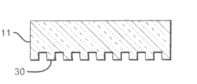
- Further dry etch processing can remove the metal hard-mask ( 21 ), binder layer ( 13 ) and dielectric layer ( 12 ), and results in a light emitting layer ( 11 ) having a surface ( 11 a ) with a high aspect ratio submicron roughness which is shown schematically in FIG. 2F as projections ( 30 ) on the surface ( 11 a ).
- the projections shown in FIG. 2F are portrayed as being symmetric in nature, but in reality the roughened surface provides non-symmetric projections, irregular, or multifaceted projections. After cleaning up any residual metal, dielectric, or binder material on the surface as needed, regular LED processing can continue.
- a 2 cm ⁇ 2 cm AnoporeTM AAO membrane (Whatman Inc., Florham Park, N.J.) template having a nominal pore size of 0.1 ⁇ M was prepared by mechanical polishing.
- a 30 nm (300 ⁇ ) gold on aluminum (“Au/Al”) metal bilayer was deposited on the polished surface of the template by electron beam evaporation or sputtering.
- the average pitch size of the resulting AAO-Au template was 200 nm and the average diameter of the pores was 100 nm.
- FIG. 3 is a scanning electron microscope (SEM) image of an AAO template prepared according Example 1.
- SEM scanning electron microscope
- the average diameter of the pores in the template is about 100 nm.
- the thickness of the metal layer is about 30 nm (300 ⁇ ).
- the surface of the template prior to metal deposition is essentially identical.
- the SEM image shown in FIG. 3 was obtained on a FEI Sirion SEM tool under an acceleration voltage of 5 kV.
- a 2 nm thick layer of GaN-based LED structure was grown on a SiC substrate wafer (CREE, Inc., Durham, N.C.) by metalorganic chemical vapor deposition (MOCVD). After the exposed p-type GaN surface (top surface) was bonded to a SiC carrier wafer through a metal-based bonding process, the SiC substrate was removed by mechanical grinding or plasma etching. A 200 nm thick layer of binder material (PMMA) was then deposited onto the n-type GaN.
- MOCVD metalorganic chemical vapor deposition
- An AAO-Au template prepared according to Example 1 was then placed on top of the layer of binder material, metal side down, using a uniformly applied pressure and bonded to the GaN layer by heating at 160° C. in a Nanonex NX-2000 tool for about 2 minutes.
- the AAO template was subsequently removed through a wet chemical etch process using either a base (e.g. KOH) solution or an acid (e.g. HNO 3 ) solution.
- An oxygen-based plasma etch process was then used to remove the binder and the final GaN etch step achieved using a chlorine-based plasma.
- a wet etch step (e.g. using aqua-regia) can be used after the GaN etch to clean up residual Au particles.
- FIG. 4 is a SEM image taken from a GaN surface, modified according to the method described in Example 2, showing the roughness and deep etch depth (approximately 1 ⁇ m) achieved using RIE in the presence of a metal hard-mask formed on the AAO template shown in FIG. 3 .
- the aspect ratio of the etched projections on the surface is about 5 and their dimensions are irregular, non-symmetrical, and multi-faceted.
- the SEM image in FIG. 4 was obtained using, a FEI Sirion SEM tool with 5 kV electron acceleration voltage and 25000 ⁇ magnification.
Landscapes
- Engineering & Computer Science (AREA)
- Manufacturing & Machinery (AREA)
- Computer Hardware Design (AREA)
- Microelectronics & Electronic Packaging (AREA)
- Power Engineering (AREA)
- Led Devices (AREA)
- Drying Of Semiconductors (AREA)
Abstract
Description
Claims (15)
Priority Applications (1)
| Application Number | Priority Date | Filing Date | Title |
|---|---|---|---|
| US13/045,246 US8507924B2 (en) | 2004-07-02 | 2011-03-10 | Light emitting diode with high aspect ratio submicron roughness for light extraction and methods of forming |
Applications Claiming Priority (4)
| Application Number | Priority Date | Filing Date | Title |
|---|---|---|---|
| US58532604P | 2004-07-02 | 2004-07-02 | |
| US11/083,460 US7534633B2 (en) | 2004-07-02 | 2005-03-17 | LED with substrate modifications for enhanced light extraction and method of making same |
| US11/498,418 US7932106B2 (en) | 2004-07-02 | 2006-08-02 | Light emitting diode with high aspect ratio submicron roughness for light extraction and methods of forming |
| US13/045,246 US8507924B2 (en) | 2004-07-02 | 2011-03-10 | Light emitting diode with high aspect ratio submicron roughness for light extraction and methods of forming |
Related Parent Applications (1)
| Application Number | Title | Priority Date | Filing Date |
|---|---|---|---|
| US11/498,418 Division US7932106B2 (en) | 2004-07-02 | 2006-08-02 | Light emitting diode with high aspect ratio submicron roughness for light extraction and methods of forming |
Publications (2)
| Publication Number | Publication Date |
|---|---|
| US20110169030A1 US20110169030A1 (en) | 2011-07-14 |
| US8507924B2 true US8507924B2 (en) | 2013-08-13 |
Family
ID=35004287
Family Applications (6)
| Application Number | Title | Priority Date | Filing Date |
|---|---|---|---|
| US11/083,460 Active US7534633B2 (en) | 2004-07-02 | 2005-03-17 | LED with substrate modifications for enhanced light extraction and method of making same |
| US11/210,713 Active US7759682B2 (en) | 2004-07-02 | 2005-08-23 | LED with substrate modifications for enhanced light extraction and method of making same |
| US11/498,418 Active 2025-11-02 US7932106B2 (en) | 2004-07-02 | 2006-08-02 | Light emitting diode with high aspect ratio submicron roughness for light extraction and methods of forming |
| US12/384,277 Active US8617909B2 (en) | 2004-07-02 | 2009-04-01 | LED with substrate modifications for enhanced light extraction and method of making same |
| US12/821,069 Active US8034647B2 (en) | 2004-07-02 | 2010-06-22 | LED with substrate modifications for enhanced light extraction and method of making same |
| US13/045,246 Active US8507924B2 (en) | 2004-07-02 | 2011-03-10 | Light emitting diode with high aspect ratio submicron roughness for light extraction and methods of forming |
Family Applications Before (5)
| Application Number | Title | Priority Date | Filing Date |
|---|---|---|---|
| US11/083,460 Active US7534633B2 (en) | 2004-07-02 | 2005-03-17 | LED with substrate modifications for enhanced light extraction and method of making same |
| US11/210,713 Active US7759682B2 (en) | 2004-07-02 | 2005-08-23 | LED with substrate modifications for enhanced light extraction and method of making same |
| US11/498,418 Active 2025-11-02 US7932106B2 (en) | 2004-07-02 | 2006-08-02 | Light emitting diode with high aspect ratio submicron roughness for light extraction and methods of forming |
| US12/384,277 Active US8617909B2 (en) | 2004-07-02 | 2009-04-01 | LED with substrate modifications for enhanced light extraction and method of making same |
| US12/821,069 Active US8034647B2 (en) | 2004-07-02 | 2010-06-22 | LED with substrate modifications for enhanced light extraction and method of making same |
Country Status (5)
| Country | Link |
|---|---|
| US (6) | US7534633B2 (en) |
| EP (1) | EP1787335B1 (en) |
| JP (1) | JP5570697B2 (en) |
| TW (1) | TWI449160B (en) |
| WO (1) | WO2006016955A1 (en) |
Cited By (1)
| Publication number | Priority date | Publication date | Assignee | Title |
|---|---|---|---|---|
| US20170271557A1 (en) * | 2014-11-24 | 2017-09-21 | Oculus Vr, Llc | Micro-LED Device |
Families Citing this family (129)
| Publication number | Priority date | Publication date | Assignee | Title |
|---|---|---|---|---|
| US7638346B2 (en) | 2001-12-24 | 2009-12-29 | Crystal Is, Inc. | Nitride semiconductor heterostructures and related methods |
| US20060005763A1 (en) | 2001-12-24 | 2006-01-12 | Crystal Is, Inc. | Method and apparatus for producing large, single-crystals of aluminum nitride |
| US8545629B2 (en) | 2001-12-24 | 2013-10-01 | Crystal Is, Inc. | Method and apparatus for producing large, single-crystals of aluminum nitride |
| US7915085B2 (en) | 2003-09-18 | 2011-03-29 | Cree, Inc. | Molded chip fabrication method |
| US7217583B2 (en) | 2004-09-21 | 2007-05-15 | Cree, Inc. | Methods of coating semiconductor light emitting elements by evaporating solvent from a suspension |
| US7265374B2 (en) * | 2005-06-10 | 2007-09-04 | Arima Computer Corporation | Light emitting semiconductor device |
| US8674375B2 (en) * | 2005-07-21 | 2014-03-18 | Cree, Inc. | Roughened high refractive index layer/LED for high light extraction |
| WO2007065018A2 (en) | 2005-12-02 | 2007-06-07 | Crystal Is, Inc. | Doped aluminum nitride crystals and methods of making them |
| JP2007165613A (en) * | 2005-12-14 | 2007-06-28 | Showa Denko Kk | Gallium-nitride compound semiconductor light emitting element, and its fabrication process |
| TWI421438B (en) * | 2005-12-21 | 2014-01-01 | 克里公司 | Lighting device |
| KR100844722B1 (en) | 2006-03-07 | 2008-07-07 | 엘지전자 주식회사 | Growth method of nanocone and Fabricating method of light emitting diode using the same |
| CN101454487B (en) | 2006-03-30 | 2013-01-23 | 晶体公司 | Methods for controllable doping of aluminum nitride bulk crystals |
| US9034103B2 (en) | 2006-03-30 | 2015-05-19 | Crystal Is, Inc. | Aluminum nitride bulk crystals having high transparency to ultraviolet light and methods of forming them |
| US8969908B2 (en) * | 2006-04-04 | 2015-03-03 | Cree, Inc. | Uniform emission LED package |
| US7943952B2 (en) | 2006-07-31 | 2011-05-17 | Cree, Inc. | Method of uniform phosphor chip coating and LED package fabricated using method |
| CN101606246B (en) | 2006-10-05 | 2012-07-04 | 三菱化学株式会社 | Light emitting device using gan led chip |
| TWI338380B (en) * | 2006-10-11 | 2011-03-01 | Chuan Yu Hung | Light emitting diode incorporating high refractive index material |
| US10295147B2 (en) | 2006-11-09 | 2019-05-21 | Cree, Inc. | LED array and method for fabricating same |
| JP5372766B2 (en) * | 2006-11-15 | 2013-12-18 | ザ リージェンツ オブ ザ ユニバーシティ オブ カリフォルニア | Spherical LED with high light extraction efficiency |
| US9318327B2 (en) * | 2006-11-28 | 2016-04-19 | Cree, Inc. | Semiconductor devices having low threading dislocations and improved light extraction and methods of making the same |
| US9771666B2 (en) | 2007-01-17 | 2017-09-26 | Crystal Is, Inc. | Defect reduction in seeded aluminum nitride crystal growth |
| US8323406B2 (en) * | 2007-01-17 | 2012-12-04 | Crystal Is, Inc. | Defect reduction in seeded aluminum nitride crystal growth |
| US8232564B2 (en) | 2007-01-22 | 2012-07-31 | Cree, Inc. | Wafer level phosphor coating technique for warm light emitting diodes |
| US9159888B2 (en) * | 2007-01-22 | 2015-10-13 | Cree, Inc. | Wafer level phosphor coating method and devices fabricated utilizing method |
| US9024349B2 (en) * | 2007-01-22 | 2015-05-05 | Cree, Inc. | Wafer level phosphor coating method and devices fabricated utilizing method |
| US8080833B2 (en) | 2007-01-26 | 2011-12-20 | Crystal Is, Inc. | Thick pseudomorphic nitride epitaxial layers |
| WO2008094464A2 (en) | 2007-01-26 | 2008-08-07 | Crystal Is, Inc. | Thick pseudomorphic nitride epitaxial layers |
| US8088220B2 (en) | 2007-05-24 | 2012-01-03 | Crystal Is, Inc. | Deep-eutectic melt growth of nitride crystals |
| US10505083B2 (en) * | 2007-07-11 | 2019-12-10 | Cree, Inc. | Coating method utilizing phosphor containment structure and devices fabricated using same |
| US9401461B2 (en) * | 2007-07-11 | 2016-07-26 | Cree, Inc. | LED chip design for white conversion |
| TWI492412B (en) * | 2007-09-07 | 2015-07-11 | Cree Inc | Wafer level phosphor coating method and devices fabricated utilizing method |
| US20100283074A1 (en) * | 2007-10-08 | 2010-11-11 | Kelley Tommie W | Light emitting diode with bonded semiconductor wavelength converter |
| DE102007057756B4 (en) * | 2007-11-30 | 2022-03-10 | OSRAM Opto Semiconductors Gesellschaft mit beschränkter Haftung | Process for producing an optoelectronic semiconductor body |
| TWI452726B (en) | 2007-11-30 | 2014-09-11 | Univ California | High light extraction efficiency nitride based light emitting diode by surface roughening |
| US20100295075A1 (en) * | 2007-12-10 | 2010-11-25 | 3M Innovative Properties Company | Down-converted light emitting diode with simplified light extraction |
| US9041285B2 (en) | 2007-12-14 | 2015-05-26 | Cree, Inc. | Phosphor distribution in LED lamps using centrifugal force |
| US8167674B2 (en) | 2007-12-14 | 2012-05-01 | Cree, Inc. | Phosphor distribution in LED lamps using centrifugal force |
| EP2234182B1 (en) * | 2007-12-28 | 2016-11-09 | Nichia Corporation | Semiconductor light emitting element and method for manufacturing the same |
| US8878219B2 (en) * | 2008-01-11 | 2014-11-04 | Cree, Inc. | Flip-chip phosphor coating method and devices fabricated utilizing method |
| US8637883B2 (en) | 2008-03-19 | 2014-01-28 | Cree, Inc. | Low index spacer layer in LED devices |
| US8877524B2 (en) * | 2008-03-31 | 2014-11-04 | Cree, Inc. | Emission tuning methods and devices fabricated utilizing methods |
| JP5167974B2 (en) * | 2008-06-16 | 2013-03-21 | 豊田合成株式会社 | Group III nitride compound semiconductor light emitting device and method of manufacturing the same |
| US8240875B2 (en) | 2008-06-25 | 2012-08-14 | Cree, Inc. | Solid state linear array modules for general illumination |
| JP5282503B2 (en) * | 2008-09-19 | 2013-09-04 | 日亜化学工業株式会社 | Semiconductor light emitting device |
| KR101363022B1 (en) * | 2008-12-23 | 2014-02-14 | 삼성디스플레이 주식회사 | Organic light emitting diode display |
| CN101800274B (en) * | 2009-02-11 | 2011-11-09 | 晶发光电股份有限公司 | Method for manufacturing semiconductor element with concave-convex base plate |
| CN101877377B (en) * | 2009-04-30 | 2011-12-14 | 比亚迪股份有限公司 | Epitaxial wafer of discrete light-emitting diode and manufacturing method thereof |
| EP2427924A1 (en) | 2009-05-05 | 2012-03-14 | 3M Innovative Properties Company | Re-emitting semiconductor carrier devices for use with leds and methods of manufacture |
| US8994071B2 (en) | 2009-05-05 | 2015-03-31 | 3M Innovative Properties Company | Semiconductor devices grown on indium-containing substrates utilizing indium depletion mechanisms |
| WO2010129412A1 (en) | 2009-05-05 | 2010-11-11 | 3M Innovative Properties Company | Re-emitting semiconductor construction with enhanced extraction efficiency |
| US8434883B2 (en) | 2009-05-11 | 2013-05-07 | SemiOptoelectronics Co., Ltd. | LLB bulb having light extracting rough surface pattern (LERSP) and method of fabrication |
| US8299341B2 (en) * | 2009-05-13 | 2012-10-30 | The California Institute Of Technology | Fabrication of vertically aligned metallic nanopillars |
| US7977123B2 (en) * | 2009-05-22 | 2011-07-12 | Lam Research Corporation | Arrangements and methods for improving bevel etch repeatability among substrates |
| CN102473817A (en) | 2009-06-30 | 2012-05-23 | 3M创新有限公司 | Cadmium-free re-emitting semiconductor construction |
| WO2011008474A1 (en) | 2009-06-30 | 2011-01-20 | 3M Innovative Properties Company | Electroluminescent devices with color adjustment based on current crowding |
| EP2449856A1 (en) | 2009-06-30 | 2012-05-09 | 3M Innovative Properties Company | White light electroluminescent devices with adjustable color temperature |
| EP2282360A1 (en) * | 2009-08-06 | 2011-02-09 | Nederlandse Organisatie voor toegepast -natuurwetenschappelijk onderzoek TNO | Opto-electric device and method for manufacturing the same |
| KR101114047B1 (en) * | 2009-10-22 | 2012-03-09 | 엘지이노텍 주식회사 | Light emitting device and method for fabricating the same |
| CN102598314A (en) * | 2009-11-03 | 2012-07-18 | 加利福尼亚大学董事会 | Superluminescent diodes by crystallographic etching |
| DE102010008603A1 (en) | 2010-02-19 | 2011-08-25 | OSRAM Opto Semiconductors GmbH, 93055 | Electrical resistance element |
| US8349626B2 (en) * | 2010-03-23 | 2013-01-08 | Gtat Corporation | Creation of low-relief texture for a photovoltaic cell |
| US9263612B2 (en) | 2010-03-23 | 2016-02-16 | California Institute Of Technology | Heterojunction wire array solar cells |
| US8538224B2 (en) | 2010-04-22 | 2013-09-17 | 3M Innovative Properties Company | OLED light extraction films having internal nanostructures and external microstructures |
| JP5806734B2 (en) | 2010-06-30 | 2015-11-10 | クリスタル アイエス, インコーポレーテッドCrystal Is, Inc. | Large single crystal growth of aluminum nitride by thermal gradient control |
| US10546846B2 (en) | 2010-07-23 | 2020-01-28 | Cree, Inc. | Light transmission control for masking appearance of solid state light sources |
| EP2641277A4 (en) | 2010-11-18 | 2016-06-15 | 3M Innovative Properties Co | Light emitting diode component comprising polysilazane bonding layer |
| US8482020B2 (en) | 2010-12-08 | 2013-07-09 | Bridgelux, Inc. | System for wafer-level phosphor deposition |
| US8841145B2 (en) | 2010-12-08 | 2014-09-23 | Bridgelux, Inc. | System for wafer-level phosphor deposition |
| JP5758116B2 (en) * | 2010-12-16 | 2015-08-05 | 株式会社ディスコ | Split method |
| US9166126B2 (en) | 2011-01-31 | 2015-10-20 | Cree, Inc. | Conformally coated light emitting devices and methods for providing the same |
| TWI426624B (en) * | 2011-02-14 | 2014-02-11 | 私立中原大學 | Method for manufacturing high efficient led |
| KR101781438B1 (en) * | 2011-06-14 | 2017-09-25 | 삼성전자주식회사 | Fabrication method of semiconductor light emitting device |
| US9337387B2 (en) | 2011-06-15 | 2016-05-10 | Sensor Electronic Technology, Inc. | Emitting device with improved extraction |
| US10522714B2 (en) | 2011-06-15 | 2019-12-31 | Sensor Electronic Technology, Inc. | Device with inverted large scale light extraction structures |
| US9142741B2 (en) | 2011-06-15 | 2015-09-22 | Sensor Electronic Technology, Inc. | Emitting device with improved extraction |
| US9741899B2 (en) | 2011-06-15 | 2017-08-22 | Sensor Electronic Technology, Inc. | Device with inverted large scale light extraction structures |
| US10319881B2 (en) | 2011-06-15 | 2019-06-11 | Sensor Electronic Technology, Inc. | Device including transparent layer with profiled surface for improved extraction |
| US9048378B2 (en) | 2011-06-15 | 2015-06-02 | Sensor Electronic Technology, Inc. | Device with inverted large scale light extraction structures |
| US10170668B2 (en) | 2011-06-21 | 2019-01-01 | Micron Technology, Inc. | Solid state lighting devices with improved current spreading and light extraction and associated methods |
| US8274091B1 (en) * | 2011-07-07 | 2012-09-25 | Yuan Ze University | Light emitting device with light extraction layer and fabricating method thereof |
| US8962359B2 (en) | 2011-07-19 | 2015-02-24 | Crystal Is, Inc. | Photon extraction from nitride ultraviolet light-emitting devices |
| CA2843415C (en) | 2011-07-29 | 2019-12-31 | University Of Saskatchewan | Polymer-based resonator antennas |
| KR101772588B1 (en) * | 2011-08-22 | 2017-09-13 | 한국전자통신연구원 | MIT device molded by Clear compound epoxy and fire detecting device including the MIT device |
| US9324560B2 (en) | 2011-09-06 | 2016-04-26 | Sensor Electronic Technology, Inc. | Patterned substrate design for layer growth |
| WO2013033841A1 (en) | 2011-09-06 | 2013-03-14 | Trilogy Environmental Systems Inc. | Hybrid desalination system |
| US10032956B2 (en) | 2011-09-06 | 2018-07-24 | Sensor Electronic Technology, Inc. | Patterned substrate design for layer growth |
| US8957440B2 (en) | 2011-10-04 | 2015-02-17 | Cree, Inc. | Light emitting devices with low packaging factor |
| CN104040735B (en) | 2011-10-06 | 2017-08-25 | 皇家飞利浦有限公司 | The surface treatment of light emitting semiconductor device |
| EP2613367A3 (en) * | 2012-01-06 | 2013-09-04 | Imec | Method for producing a led device . |
| WO2013126432A1 (en) | 2012-02-21 | 2013-08-29 | California Institute Of Technology | Axially-integrated epitaxially-grown tandem wire arrays |
| US9947816B2 (en) | 2012-04-03 | 2018-04-17 | California Institute Of Technology | Semiconductor structures for fuel generation |
| CN103378223B (en) * | 2012-04-25 | 2016-07-06 | 清华大学 | The preparation method of epitaxial structure |
| EP2870641B1 (en) * | 2012-07-05 | 2020-05-13 | Lumileds Holding B.V. | Phosphor separated from led by transparent spacer |
| EP2896077B1 (en) * | 2012-09-17 | 2019-01-16 | Lumileds Holding B.V. | Light emitting device including shaped substrate |
| CN109979925B (en) * | 2012-12-06 | 2024-03-01 | 首尔伟傲世有限公司 | Light emitting diode |
| US9536924B2 (en) * | 2012-12-06 | 2017-01-03 | Seoul Viosys Co., Ltd. | Light-emitting diode and application therefor |
| US9553223B2 (en) | 2013-01-24 | 2017-01-24 | California Institute Of Technology | Method for alignment of microwires |
| CA2899236C (en) * | 2013-01-31 | 2023-02-14 | Atabak RASHIDIAN | Meta-material resonator antennas |
| CN108511567A (en) | 2013-03-15 | 2018-09-07 | 晶体公司 | With the counterfeit plane contact with electronics and photoelectric device |
| FR3009428B1 (en) * | 2013-08-05 | 2015-08-07 | Commissariat Energie Atomique | METHOD FOR MANUFACTURING SEMICONDUCTOR STRUCTURE WITH TEMPORARY COLLAGE VIA METAL LAYERS |
| US10784583B2 (en) | 2013-12-20 | 2020-09-22 | University Of Saskatchewan | Dielectric resonator antenna arrays |
| CN103794688B (en) * | 2014-02-13 | 2016-11-09 | 厦门大学 | A kind of preparation method of GaN-based LED with photonic crystal structure |
| US10147854B2 (en) | 2014-05-10 | 2018-12-04 | Sensor Electronic Technology, Inc. | Packaging for ultraviolet optoelectronic device |
| US20160064631A1 (en) * | 2014-05-10 | 2016-03-03 | Sensor Electronic Technology, Inc. | Packaging for Ultraviolet Optoelectronic Device |
| US9263653B2 (en) | 2014-05-15 | 2016-02-16 | Empire Technology Development Llc | Light-emissive devices and light-emissive displays |
| US9633883B2 (en) | 2015-03-20 | 2017-04-25 | Rohinni, LLC | Apparatus for transfer of semiconductor devices |
| KR101729683B1 (en) * | 2015-09-16 | 2017-04-25 | 한국기계연구원 | Manufacturing method of wire grid polarizer |
| US10400322B2 (en) | 2015-12-04 | 2019-09-03 | The University Of Florida Research Foundation, Inc. | Fabrication of thermally stable nanocavities and particle-in-cavity nanostructures |
| US10461221B2 (en) | 2016-01-18 | 2019-10-29 | Sensor Electronic Technology, Inc. | Semiconductor device with improved light propagation |
| JP6690814B2 (en) | 2016-01-27 | 2020-04-28 | エルジー・ケム・リミテッド | Film mask, method for manufacturing the same, and pattern forming method using the same |
| EP3410215B1 (en) | 2016-01-27 | 2020-06-17 | LG Chem, Ltd. | Film mask, method for manufacturing same, and method for forming pattern using film mask and pattern formed thereby |
| US11029596B2 (en) | 2016-01-27 | 2021-06-08 | Lg Chem, Ltd. | Film mask, method for manufacturing same, and method for forming pattern using film mask and pattern formed thereby |
| WO2018038927A1 (en) | 2016-08-26 | 2018-03-01 | The Penn State Research Foundation | High light-extraction efficiency (lee) light-emitting diode (led) |
| JP6871706B2 (en) * | 2016-09-30 | 2021-05-12 | 日機装株式会社 | Manufacturing method of semiconductor light emitting device |
| US10141215B2 (en) | 2016-11-03 | 2018-11-27 | Rohinni, LLC | Compliant needle for direct transfer of semiconductor devices |
| US10504767B2 (en) | 2016-11-23 | 2019-12-10 | Rohinni, LLC | Direct transfer apparatus for a pattern array of semiconductor device die |
| US10471545B2 (en) | 2016-11-23 | 2019-11-12 | Rohinni, LLC | Top-side laser for direct transfer of semiconductor devices |
| US10062588B2 (en) | 2017-01-18 | 2018-08-28 | Rohinni, LLC | Flexible support substrate for transfer of semiconductor devices |
| WO2019083729A1 (en) * | 2017-10-23 | 2019-05-02 | Trustees Of Boston University | Enhanced thermal transport across interfaces |
| US10410905B1 (en) | 2018-05-12 | 2019-09-10 | Rohinni, LLC | Method and apparatus for direct transfer of multiple semiconductor devices |
| US11094571B2 (en) | 2018-09-28 | 2021-08-17 | Rohinni, LLC | Apparatus to increase transferspeed of semiconductor devices with micro-adjustment |
| CN109585685B (en) * | 2018-12-07 | 2021-06-01 | 纳晶科技股份有限公司 | Light extraction structure, manufacturing method thereof and light emitting device |
| WO2020146318A1 (en) | 2019-01-07 | 2020-07-16 | Glint Photonics, Inc. | Antireflective structures for light emitting diodes |
| CN112864296B (en) * | 2019-01-29 | 2022-06-28 | 泉州三安半导体科技有限公司 | LED packaging device |
| DE102019114169A1 (en) * | 2019-05-27 | 2020-12-03 | OSRAM Opto Semiconductors Gesellschaft mit beschränkter Haftung | OPTOELECTRONIC SEMICONDUCTOR COMPONENT WITH CONNECTING AREAS AND METHOD FOR MANUFACTURING THE OPTOELECTRONIC SEMICONDUCTOR COMPONENT |
| CN110600598B (en) * | 2019-08-21 | 2021-02-05 | 苏州紫灿科技有限公司 | Inverted ultraviolet LED with double-layer nano array structure and preparation method |
| JP2021170595A (en) | 2020-04-15 | 2021-10-28 | 国立大学法人東海国立大学機構 | Gallium nitride semiconductor device and manufacturing method thereof |
| US11088093B1 (en) * | 2020-05-28 | 2021-08-10 | X-Celeprint Limited | Micro-component anti-stiction structures |
| FR3132593A1 (en) * | 2022-02-08 | 2023-08-11 | Centre National De La Recherche Scientifique - Cnrs - | CREATING A RADIATION OUTPUT WINDOW FOR A PHOTOEMITTING COMPONENT |
Citations (119)
| Publication number | Priority date | Publication date | Assignee | Title |
|---|---|---|---|---|
| US3896479A (en) | 1973-09-24 | 1975-07-22 | Bell Telephone Labor Inc | Reduced stresses in iii-v semiconductor devices |
| US4152044A (en) | 1977-06-17 | 1979-05-01 | International Telephone And Telegraph Corporation | Galium aluminum arsenide graded index waveguide |
| FR2586844A1 (en) | 1985-08-27 | 1987-03-06 | Sofrela Sa | Signalling device using light-emitting diodes |
| US4675575A (en) | 1984-07-13 | 1987-06-23 | E & G Enterprises | Light-emitting diode assemblies and systems therefore |
| EP0272985A2 (en) | 1986-12-20 | 1988-06-29 | Fujitsu Limited | Constant current semiconductor device |
| JPS63288061A (en) | 1987-05-20 | 1988-11-25 | Fujitsu Ltd | Semiconductor negative resistance element |
| US4946547A (en) | 1989-10-13 | 1990-08-07 | Cree Research, Inc. | Method of preparing silicon carbide surfaces for crystal growth |
| US4963948A (en) | 1986-12-20 | 1990-10-16 | Fujitsu Limited | Semiconductor device having level shift diode |
| US5034783A (en) | 1990-07-27 | 1991-07-23 | At&T Bell Laboratories | Semiconductor device including cascadable polarization independent heterostructure |
| JPH0575101A (en) | 1991-09-10 | 1993-03-26 | Sanken Electric Co Ltd | Semiconductor device having schottky barrier |
| US5200022A (en) | 1990-10-03 | 1993-04-06 | Cree Research, Inc. | Method of improving mechanically prepared substrate surfaces of alpha silicon carbide for deposition of beta silicon carbide thereon and resulting product |
| JPH05283672A (en) | 1992-03-30 | 1993-10-29 | Murata Mfg Co Ltd | Schottky barrier semiconductor device |
| JPH06268257A (en) | 1993-03-12 | 1994-09-22 | Nichia Chem Ind Ltd | Gallium nitride compound semiconductor light emitting element |
| USRE34861E (en) | 1987-10-26 | 1995-02-14 | North Carolina State University | Sublimation of silicon carbide to produce large, device quality single crystals of silicon carbide |
| JPH07162038A (en) | 1993-12-10 | 1995-06-23 | Nichia Chem Ind Ltd | Gallium nitride compound semiconductor light emitting diode |
| JPH07176826A (en) | 1993-12-17 | 1995-07-14 | Nichia Chem Ind Ltd | Gallium nitride compound semiconductor laser element |
| US5477436A (en) | 1992-08-29 | 1995-12-19 | Robert Bosch Gmbh | Illuminating device for motor vehicles |
| JPH08162671A (en) | 1994-10-07 | 1996-06-21 | Nichia Chem Ind Ltd | Nitride semiconductor light emitting diode |
| JPH08274414A (en) | 1995-01-31 | 1996-10-18 | Nichia Chem Ind Ltd | Nitride semiconductor laser element |
| US5612567A (en) | 1996-05-13 | 1997-03-18 | North Carolina State University | Schottky barrier rectifiers and methods of forming same |
| US5628917A (en) | 1995-02-03 | 1997-05-13 | Cornell Research Foundation, Inc. | Masking process for fabricating ultra-high aspect ratio, wafer-free micro-opto-electromechanical structures |
| JPH09148678A (en) | 1995-11-24 | 1997-06-06 | Nichia Chem Ind Ltd | Nitride semiconductor light emitting element |
| JPH09153642A (en) | 1995-09-29 | 1997-06-10 | Nichia Chem Ind Ltd | Nitride semiconductor light emitting element |
| JPH09162444A (en) | 1995-12-11 | 1997-06-20 | Nichia Chem Ind Ltd | Nitride semiconductor multi-color light emitting device and its production |
| JPH09219556A (en) | 1995-11-24 | 1997-08-19 | Nichia Chem Ind Ltd | Nitride semiconductor laser element |
| JPH09330630A (en) | 1996-06-12 | 1997-12-22 | Nec Corp | Lighting switch |
| US5705321A (en) * | 1993-09-30 | 1998-01-06 | The University Of New Mexico | Method for manufacture of quantum sized periodic structures in Si materials |
| WO1998031055A1 (en) | 1997-01-09 | 1998-07-16 | Nichia Chemical Industries, Ltd. | Nitride semiconductor device |
| FR2759188A1 (en) | 1997-01-31 | 1998-08-07 | Thery Hindrick | Signal light used for controlling road traffic |
| WO1998037585A1 (en) | 1997-02-24 | 1998-08-27 | Minnesota Mining And Manufacturing Company | Passivation capping layer for ohmic contact in ii-vi semiconductor light transducing device |
| EP0881666A2 (en) | 1997-05-26 | 1998-12-02 | Sony Corporation | P-type nitrogen compound semiconductor and method of manufacturing same |
| WO1999005728A1 (en) | 1997-07-25 | 1999-02-04 | Nichia Chemical Industries, Ltd. | Nitride semiconductor device |
| JPH1140850A (en) | 1997-07-23 | 1999-02-12 | Toyoda Gosei Co Ltd | Manufacture of iii nitride compound semiconductor element |
| EP0936682A1 (en) | 1996-07-29 | 1999-08-18 | Nichia Chemical Industries, Ltd. | Light emitting device and display device |
| WO1999046822A1 (en) | 1998-03-12 | 1999-09-16 | Nichia Chemical Industries, Ltd. | Nitride semiconductor device |
| JPH11330552A (en) | 1998-05-18 | 1999-11-30 | Nichia Chem Ind Ltd | Nitride semiconductor light-emitting element and light-emitting device |
| JP2000049363A (en) | 1998-07-31 | 2000-02-18 | Denso Corp | Schottky diode and its manufacture |
| JP2000068594A (en) | 1997-09-01 | 2000-03-03 | Nichia Chem Ind Ltd | Nitride semiconductor element |
| US6046464A (en) | 1995-03-29 | 2000-04-04 | North Carolina State University | Integrated heterostructures of group III-V nitride semiconductor materials including epitaxial ohmic contact comprising multiple quantum well |
| JP2000133883A (en) | 1998-10-22 | 2000-05-12 | Nichia Chem Ind Ltd | Nitride semiconductor element |
| US6063699A (en) * | 1998-08-19 | 2000-05-16 | International Business Machines Corporation | Methods for making high-aspect ratio holes in semiconductor and its application to a gate damascene process for sub- 0.05 micron mosfets |
| JP2000150920A (en) | 1998-11-12 | 2000-05-30 | Nippon Telegr & Teleph Corp <Ntt> | Manufacture of schottky junction semiconductor diode device |
| JP2000150956A (en) | 1998-11-18 | 2000-05-30 | Nichia Chem Ind Ltd | Nitride semiconductor light emitting element |
| JP2000244072A (en) | 1998-10-06 | 2000-09-08 | Nichia Chem Ind Ltd | Nitride semiconductor element |
| JP2000307149A (en) | 1999-04-21 | 2000-11-02 | Nichia Chem Ind Ltd | Nitride semiconductor element |
| US6150672A (en) | 1997-01-16 | 2000-11-21 | Agilent Technologies | P-type group III-nitride semiconductor device |
| WO2000076004A1 (en) | 1999-06-07 | 2000-12-14 | Nichia Corporation | Nitride semiconductor device |
| JP2001168471A (en) | 1998-12-15 | 2001-06-22 | Nichia Chem Ind Ltd | Nitride semiconductor light-emitting element |
| JP2001332770A (en) | 2000-05-23 | 2001-11-30 | Koha Co Ltd | Resin-sealing method of led chip |
| US6330111B1 (en) | 2000-06-13 | 2001-12-11 | Kenneth J. Myers, Edward Greenberg | Lighting elements including light emitting diodes, microprism sheet, reflector, and diffusing agent |
| US6331915B1 (en) | 2000-06-13 | 2001-12-18 | Kenneth J. Myers | Lighting element including light emitting diodes, microprism sheet, reflector, and diffusing agent |
| US6331944B1 (en) | 2000-04-13 | 2001-12-18 | International Business Machines Corporation | Magnetic random access memory using a series tunnel element select mechanism |
| WO2002005399A1 (en) | 2000-07-07 | 2002-01-17 | Nichia Corporation | Nitride semiconductor device |
| WO2002011212A1 (en) | 2000-07-27 | 2002-02-07 | Caldus Semiconductor, Inc. | W/wc/tac ohmic and rectifying contacts on sic |
| US20020015013A1 (en) | 2000-06-28 | 2002-02-07 | Larry Ragle | Integrated color LED chip |
| FR2814220A1 (en) | 2000-09-18 | 2002-03-22 | Koito Mfg Co Ltd | VEHICLE LAMP COMPRISING SEVERAL PHOTOEMISSIVE DIODES |
| US20020054495A1 (en) | 2000-09-18 | 2002-05-09 | Koito Manufacturing Co., Ltd. | Vehicle lamp |
| US6389051B1 (en) | 1999-04-09 | 2002-05-14 | Xerox Corporation | Structure and method for asymmetric waveguide nitride laser diode |
| US6410942B1 (en) | 1999-12-03 | 2002-06-25 | Cree Lighting Company | Enhanced light extraction through the use of micro-LED arrays |
| US6482711B1 (en) | 1999-10-28 | 2002-11-19 | Hrl Laboratories, Llc | InPSb/InAs BJT device and method of making |
| JP2002543594A (en) | 1999-04-22 | 2002-12-17 | オスラム オプト セミコンダクターズ ゲゼルシャフト ミット ベシュレンクテル ハフツング | LED light source with lens |
| US6504179B1 (en) | 2000-05-29 | 2003-01-07 | Patent-Treuhand-Gesellschaft Fur Elektrische Gluhlampen Mbh | Led-based white-emitting illumination unit |
| US20030015708A1 (en) | 2001-07-23 | 2003-01-23 | Primit Parikh | Gallium nitride based diodes with low forward voltage and low reverse current operation |
| US20030020069A1 (en) | 2001-07-25 | 2003-01-30 | Motorola, Inc. | Structure and method for optimizing transmission media through dielectric layering and doping in semiconductor structures and devices utilizing the formation of a compliant substrate |
| US6526082B1 (en) | 2000-06-02 | 2003-02-25 | Lumileds Lighting U.S., Llc | P-contact for GaN-based semiconductors utilizing a reverse-biased tunnel junction |
| US20030085409A1 (en) | 2001-11-02 | 2003-05-08 | Yu-Chen Shen | Indium gallium nitride separate confinement heterostructure light emitting devices |
| US20030165169A1 (en) | 2002-03-01 | 2003-09-04 | Opnext Japan, Inc. | Semiconductor laser diode and optical module |
| JP2003258313A (en) | 2002-03-05 | 2003-09-12 | Rohm Co Ltd | Structure of light emitting device using led chip and its manufacturing method |
| EP1349202A2 (en) | 2002-03-28 | 2003-10-01 | Rohm Co., Ltd. | Semiconductor device and method of manufacturing the same |
| WO2003080763A1 (en) | 2002-03-25 | 2003-10-02 | Philips Intellectual Property & Standards Gmbh | Tri-color white light led lamp |
| JP2003318449A (en) | 2003-05-20 | 2003-11-07 | Sanyo Electric Co Ltd | Led light source and its fabricating method |
| US20030218183A1 (en) | 2001-12-06 | 2003-11-27 | Miroslav Micovic | High power-low noise microwave GaN heterojunction field effet transistor |
| US6657236B1 (en) | 1999-12-03 | 2003-12-02 | Cree Lighting Company | Enhanced light extraction in LEDs through the use of internal and external optical elements |
| US6693357B1 (en) * | 2003-03-13 | 2004-02-17 | Texas Instruments Incorporated | Methods and semiconductor devices with wiring layer fill structures to improve planarization uniformity |
| US6746889B1 (en) | 2001-03-27 | 2004-06-08 | Emcore Corporation | Optoelectronic device with improved light extraction |
| US6784463B2 (en) | 1997-06-03 | 2004-08-31 | Lumileds Lighting U.S., Llc | III-Phospide and III-Arsenide flip chip light-emitting devices |
| WO2004084316A2 (en) | 2003-03-20 | 2004-09-30 | Acol Technologies S.A. | Light emitting diode package providing phosphor amount control |
| US20040207313A1 (en) | 2003-04-21 | 2004-10-21 | Sharp Kabushiki Kaisha | LED device and portable telephone, digital camera and LCD apparatus using the same |
| US20040206966A1 (en) | 2003-03-24 | 2004-10-21 | Kabushiki Kaisha Toshiba | Group-III nitride semiconductor stack, method of manufacturing the same, and group-III nitride semiconductor device |
| US6878634B2 (en) | 2002-04-10 | 2005-04-12 | Canon Kabushiki Kaisha | Structure having recesses and projections, method of manufacturing structure, and functional device |
| US6878975B2 (en) | 2002-02-08 | 2005-04-12 | Agilent Technologies, Inc. | Polarization field enhanced tunnel structures |
| US20050077535A1 (en) | 2003-10-08 | 2005-04-14 | Joinscan Electronics Co., Ltd | LED and its manufacturing process |
| US6882051B2 (en) | 2001-03-30 | 2005-04-19 | The Regents Of The University Of California | Nanowires, nanostructures and devices fabricated therefrom |
| US6884647B2 (en) | 2000-09-22 | 2005-04-26 | Shiro Sakai | Method for roughening semiconductor surface |
| US20050117320A1 (en) | 2003-11-14 | 2005-06-02 | Hon Hai Precision Industry Co., Ltd. | Light-emitting diode and backlight system using the same |
| US20050152127A1 (en) | 2003-12-19 | 2005-07-14 | Takayuki Kamiya | LED lamp apparatus |
| US20050158637A1 (en) | 2004-01-15 | 2005-07-21 | Samsung Electronics Co., Ltd. | Template, method of forming the template and method of forming a pattern on a semiconductor device using the template |
| US20050173728A1 (en) | 2004-02-05 | 2005-08-11 | Saxler Adam W. | Nitride heterojunction transistors having charge-transfer induced energy barriers and methods of fabricating the same |
| US20050173692A1 (en) | 2002-12-27 | 2005-08-11 | Park Young H. | Vertical GaN light emitting diode and method for manufacturing the same |
| US6932497B1 (en) | 2003-12-17 | 2005-08-23 | Jean-San Huang | Signal light and rear-view mirror arrangement |
| JP2005228833A (en) | 2004-02-12 | 2005-08-25 | Mitsubishi Cable Ind Ltd | Light-emitting device, illumination device, and display device |
| US20050219668A1 (en) | 2002-05-24 | 2005-10-06 | Heriot-Watt University | Synthetic colour hologram |
| US20050224829A1 (en) | 2004-04-06 | 2005-10-13 | Negley Gerald H | Light-emitting devices having multiple encapsulation layers with at least one of the encapsulation layers including nanoparticles and methods of forming the same |
| WO2005098976A2 (en) | 2004-03-31 | 2005-10-20 | Cree, Inc. | Semiconductor light emitting devices including a luminescent conversion element and methods for packaging the same |
| US20060034576A1 (en) | 2004-08-16 | 2006-02-16 | Merritt Scott A | Superluminescent diodes having high output power and reduced internal reflections |
| US20060081862A1 (en) | 2004-10-14 | 2006-04-20 | Chua Janet B Y | Device and method for emitting output light using quantum dots and non-quantum fluorescent material |
| EP1653255A2 (en) | 2004-10-29 | 2006-05-03 | Pentair Water Pool and Spa, Inc. | Selectable beam lens for underwater light |
| US20060113638A1 (en) * | 2003-05-02 | 2006-06-01 | Maaskant Pleun P | Light emitting diodes and the manufacture thereof |
| EP1681509A1 (en) | 2005-01-17 | 2006-07-19 | Omron Corporation | Luminescent light source and luminescent source array |
| US7083490B2 (en) | 2002-06-07 | 2006-08-01 | Philips Lumileds Lighting Company, Llc | Light-emitting devices utilizing nanoparticles |
| US7087936B2 (en) | 2003-04-30 | 2006-08-08 | Cree, Inc. | Methods of forming light-emitting devices having an antireflective layer that has a graded index of refraction |
| US20060220046A1 (en) | 2005-03-04 | 2006-10-05 | Chuan-Pei Yu | Led |
| US20060267031A1 (en) | 2000-12-28 | 2006-11-30 | Stefan Tasch | Light source with a light-emitting element |
| US20070007558A1 (en) | 2005-06-27 | 2007-01-11 | Mazzochette Joseph B | Light emitting diode package and method for making same |
| US20070025231A1 (en) | 2005-07-29 | 2007-02-01 | Masanao Ochiai | Semiconductor laser device |
| JP2007036010A (en) | 2005-07-28 | 2007-02-08 | Toshiba Corp | Schottky barrier diode equipment and its manufacturing method |
| US20070041101A1 (en) | 2005-08-22 | 2007-02-22 | Eastman Kodak Company | Zoom lens system having variable power element |
| US7194170B2 (en) | 2004-11-04 | 2007-03-20 | Palo Alto Research Center Incorporated | Elastic microchannel collimating arrays and method of fabrication |
| US7214626B2 (en) | 2005-08-24 | 2007-05-08 | United Microelectronics Corp. | Etching process for decreasing mask defect |
| US20070164487A1 (en) | 2004-05-07 | 2007-07-19 | Marc Beck | Method for imprint lithography at constant temperature |
| US20070268694A1 (en) | 2006-04-18 | 2007-11-22 | Lamina Ceramics, Inc. | Optical devices for controlled color mixing |
| US20080036364A1 (en) | 2006-08-10 | 2008-02-14 | Intematix Corporation | Two-phase yellow phosphor with self-adjusting emission wavelength |
| US20080074032A1 (en) | 2004-04-19 | 2008-03-27 | Tadashi Yano | Method for Fabricating Led Illumination Light Source and Led Illumination Light Source |
| US7374968B2 (en) | 2005-01-28 | 2008-05-20 | Hewlett-Packard Development Company, L.P. | Method of utilizing a contact printing stamp |
| JP2007189239A5 (en) | 2007-02-01 | 2008-06-05 | ||
| US7491626B2 (en) | 2005-06-20 | 2009-02-17 | Sensor Electronic Technology, Inc. | Layer growth using metal film and/or islands |
| EP2048718A1 (en) | 2007-10-10 | 2009-04-15 | Cree, Inc. | Multiple conversion material light emitting diode package and method of fabricating same |
| US7662544B2 (en) * | 2004-04-23 | 2010-02-16 | Schott Ag | Method for manufacturing a master, master, method for manufacturing optical elements and optical element |
| US20110193057A1 (en) | 2007-11-30 | 2011-08-11 | Osram Opto Semiconductors Gmbh | LED Having Current Spreading Layer |
Family Cites Families (199)
| Publication number | Priority date | Publication date | Assignee | Title |
|---|---|---|---|---|
| JPS508494Y1 (en) | 1970-11-13 | 1975-03-14 | ||
| JPS5722581Y2 (en) * | 1979-08-21 | 1982-05-17 | ||
| US4476620A (en) * | 1979-10-19 | 1984-10-16 | Matsushita Electric Industrial Co., Ltd. | Method of making a gallium nitride light-emitting diode |
| DE3128187A1 (en) | 1981-07-16 | 1983-02-03 | Joachim 8068 Pfaffenhofen Sieg | OPTO-ELECTRONIC COMPONENT |
| JPS6159886A (en) | 1984-08-31 | 1986-03-27 | Fujitsu Ltd | Manufacture of photosemiconductor device |
| US4981551A (en) | 1987-11-03 | 1991-01-01 | North Carolina State University | Dry etching of silicon carbide |
| US4865685A (en) * | 1987-11-03 | 1989-09-12 | North Carolina State University | Dry etching of silicon carbide |
| JPH0770755B2 (en) * | 1988-01-21 | 1995-07-31 | 三菱化学株式会社 | High brightness LED epitaxial substrate and method of manufacturing the same |
| US4912532A (en) * | 1988-08-26 | 1990-03-27 | Hewlett-Packard Company | Electro-optical device with inverted transparent substrate and method for making same |
| EP0405757A3 (en) * | 1989-06-27 | 1991-01-30 | Hewlett-Packard Company | High efficiency light-emitting diode |
| US5087949A (en) * | 1989-06-27 | 1992-02-11 | Hewlett-Packard Company | Light-emitting diode with diagonal faces |
| US5103271A (en) * | 1989-09-28 | 1992-04-07 | Kabushiki Kaisha Toshiba | Semiconductor light emitting device and method of fabricating the same |
| JPH0644567B2 (en) * | 1989-12-18 | 1994-06-08 | 株式会社日立製作所 | Semiconductor shape improvement method |
| JP2765256B2 (en) * | 1991-04-10 | 1998-06-11 | 日立電線株式会社 | Light emitting diode |
| FR2679253B1 (en) * | 1991-07-15 | 1994-09-02 | Pasteur Institut | CYCLOHEXIMIDE RESISTANCE PROTEINS. USE AS A SELECTION MARKER FOR EXAMPLE TO CONTROL THE TRANSFER OF NUCLEIC ACIDS. |
| US5198390A (en) * | 1992-01-16 | 1993-03-30 | Cornell Research Foundation, Inc. | RIE process for fabricating submicron, silicon electromechanical structures |
| US5298767A (en) | 1992-10-06 | 1994-03-29 | Kulite Semiconductor Products, Inc. | Porous silicon carbide (SiC) semiconductor device |
| US5376580A (en) * | 1993-03-19 | 1994-12-27 | Hewlett-Packard Company | Wafer bonding of light emitting diode layers |
| GB9320291D0 (en) | 1993-10-01 | 1993-11-17 | Brown John H | Optical directing devices for light emitting diodes |
| US5656832A (en) * | 1994-03-09 | 1997-08-12 | Kabushiki Kaisha Toshiba | Semiconductor heterojunction device with ALN buffer layer of 3nm-10nm average film thickness |
| JPH08148280A (en) | 1994-04-14 | 1996-06-07 | Toshiba Corp | Semiconductor device and manufacture therefor |
| JP2994219B2 (en) | 1994-05-24 | 1999-12-27 | シャープ株式会社 | Method for manufacturing semiconductor device |
| US5614734A (en) | 1995-03-15 | 1997-03-25 | Yale University | High efficency LED structure |
| US5900650A (en) * | 1995-08-31 | 1999-05-04 | Kabushiki Kaisha Toshiba | Semiconductor device and method of manufacturing the same |
| US5779924A (en) * | 1996-03-22 | 1998-07-14 | Hewlett-Packard Company | Ordered interface texturing for a light emitting device |
| US5985687A (en) | 1996-04-12 | 1999-11-16 | The Regents Of The University Of California | Method for making cleaved facets for lasers fabricated with gallium nitride and other noncubic materials |
| US5803579A (en) | 1996-06-13 | 1998-09-08 | Gentex Corporation | Illuminator assembly incorporating light emitting diodes |
| US20040239243A1 (en) | 1996-06-13 | 2004-12-02 | Roberts John K. | Light emitting assembly |
| US6550949B1 (en) | 1996-06-13 | 2003-04-22 | Gentex Corporation | Systems and components for enhancing rear vision from a vehicle |
| US6030848A (en) * | 1996-06-28 | 2000-02-29 | Kabushiki Kaisha Toshiba | Method for manufacturing a GaN-based compound semiconductor light emitting device |
| DE19640594B4 (en) * | 1996-10-01 | 2016-08-04 | Osram Gmbh | module |
| JPH10163535A (en) | 1996-11-27 | 1998-06-19 | Kasei Optonix Co Ltd | White light-emitting element |
| EP0960353B1 (en) | 1997-02-13 | 2010-04-14 | Honeywell International Inc. | Illumination system with light recycling to enhance brightness |
| US5939732A (en) | 1997-05-22 | 1999-08-17 | Kulite Semiconductor Products, Inc. | Vertical cavity-emitting porous silicon carbide light-emitting diode device and preparation thereof |
| DE19723176C1 (en) | 1997-06-03 | 1998-08-27 | Daimler Benz Ag | Semiconductor device with alternate p-n and Schottky junctions |
| US5888886A (en) * | 1997-06-30 | 1999-03-30 | Sdl, Inc. | Method of doping gan layers p-type for device fabrication |
| US7014336B1 (en) | 1999-11-18 | 2006-03-21 | Color Kinetics Incorporated | Systems and methods for generating and modulating illumination conditions |
| US6071795A (en) * | 1998-01-23 | 2000-06-06 | The Regents Of The University Of California | Separation of thin films from transparent substrates by selective optical processing |
| JPH11238913A (en) | 1998-02-20 | 1999-08-31 | Namiki Precision Jewel Co Ltd | Semiconductor light-emitting device chip |
| DE19813269A1 (en) * | 1998-03-25 | 1999-09-30 | Hoechst Diafoil Gmbh | Sealable polyester film with high oxygen barrier, process for its production and its use |
| DE19829197C2 (en) | 1998-06-30 | 2002-06-20 | Siemens Ag | Component emitting and / or receiving radiation |
| US6225647B1 (en) | 1998-07-27 | 2001-05-01 | Kulite Semiconductor Products, Inc. | Passivation of porous semiconductors for improved optoelectronic device performance and light-emitting diode based on same |
| US5959316A (en) | 1998-09-01 | 1999-09-28 | Hewlett-Packard Company | Multiple encapsulation of phosphor-LED devices |
| EP1115163A4 (en) | 1998-09-10 | 2001-12-05 | Rohm Co Ltd | Semiconductor light-emitting device and method for manufacturing the same |
| JP3525061B2 (en) * | 1998-09-25 | 2004-05-10 | 株式会社東芝 | Method for manufacturing semiconductor light emitting device |
| WO2000019546A1 (en) | 1998-09-28 | 2000-04-06 | Koninklijke Philips Electronics N.V. | Lighting system |
| US6274924B1 (en) * | 1998-11-05 | 2001-08-14 | Lumileds Lighting, U.S. Llc | Surface mountable LED package |
| US6429583B1 (en) | 1998-11-30 | 2002-08-06 | General Electric Company | Light emitting device with ba2mgsi2o7:eu2+, ba2sio4:eu2+, or (srxcay ba1-x-y)(a1zga1-z)2sr:eu2+phosphors |
| US6744800B1 (en) * | 1998-12-30 | 2004-06-01 | Xerox Corporation | Method and structure for nitride based laser diode arrays on an insulating substrate |
| US6212213B1 (en) | 1999-01-29 | 2001-04-03 | Agilent Technologies, Inc. | Projector light source utilizing a solid state green light source |
| US6320206B1 (en) * | 1999-02-05 | 2001-11-20 | Lumileds Lighting, U.S., Llc | Light emitting devices having wafer bonded aluminum gallium indium nitride structures and mirror stacks |
| US20010042866A1 (en) * | 1999-02-05 | 2001-11-22 | Carrie Carter Coman | Inxalygazn optical emitters fabricated via substrate removal |
| US6258699B1 (en) * | 1999-05-10 | 2001-07-10 | Visual Photonics Epitaxy Co., Ltd. | Light emitting diode with a permanent subtrate of transparent glass or quartz and the method for manufacturing the same |
| EP1059668A3 (en) | 1999-06-09 | 2007-07-18 | Sanyo Electric Co., Ltd. | Hybrid integrated circuit device |
| US6489637B1 (en) | 1999-06-09 | 2002-12-03 | Sanyo Electric Co., Ltd. | Hybrid integrated circuit device |
| JP2000353826A (en) | 1999-06-09 | 2000-12-19 | Sanyo Electric Co Ltd | Hybrid integrated circuit device and light irradiating device |
| DE60042187D1 (en) * | 1999-06-09 | 2009-06-25 | Toshiba Kawasaki Kk | Bond-type semiconductor substrate, semiconductor light-emitting device, and manufacturing method |
| JP2000357820A (en) * | 1999-06-15 | 2000-12-26 | Pioneer Electronic Corp | Gallium nitride semiconductor light emitting element and its manufacture |
| KR100425566B1 (en) | 1999-06-23 | 2004-04-01 | 가부시키가이샤 시티즌 덴시 | Light emitting diode |
| DE19931689A1 (en) | 1999-07-08 | 2001-01-11 | Patent Treuhand Ges Fuer Elektrische Gluehlampen Mbh | Planar LED assembly on thermally-conductive board, increases cooling, component packing density and life, whilst permitting active device integration to form display- or illumination panel in or on e.g. vehicle |
| JP4055303B2 (en) * | 1999-10-12 | 2008-03-05 | 豊田合成株式会社 | Gallium nitride compound semiconductor and semiconductor device |
| DE19952932C1 (en) | 1999-11-03 | 2001-05-03 | Osram Opto Semiconductors Gmbh | LED white light source with broadband excitation |
| US6513949B1 (en) | 1999-12-02 | 2003-02-04 | Koninklijke Philips Electronics N.V. | LED/phosphor-LED hybrid lighting systems |
| US6350041B1 (en) | 1999-12-03 | 2002-02-26 | Cree Lighting Company | High output radial dispersing lamp using a solid state light source |
| US6646292B2 (en) | 1999-12-22 | 2003-11-11 | Lumileds Lighting, U.S., Llc | Semiconductor light emitting device and method |
| US6573537B1 (en) | 1999-12-22 | 2003-06-03 | Lumileds Lighting, U.S., Llc | Highly reflective ohmic contacts to III-nitride flip-chip LEDs |
| JP2000315826A (en) | 2000-01-01 | 2000-11-14 | Nichia Chem Ind Ltd | Light emitting device, formation thereof, gun type light emitting diode, chip type led |
| TW465123B (en) | 2000-02-02 | 2001-11-21 | Ind Tech Res Inst | High power white light LED |
| WO2001059851A1 (en) | 2000-02-09 | 2001-08-16 | Nippon Leiz Corporation | Light source |
| DE10008583A1 (en) * | 2000-02-24 | 2001-09-13 | Osram Opto Semiconductors Gmbh | Production of an optically transparent substrate comprises epitaxially growing a substrate layer on a substrate, connecting the substrate layer to the side with an optically transparent layer, and removing the substrate |
| US6538371B1 (en) | 2000-03-27 | 2003-03-25 | The General Electric Company | White light illumination system with improved color output |
| JP4060511B2 (en) * | 2000-03-28 | 2008-03-12 | パイオニア株式会社 | Method for separating nitride semiconductor device |
| JP2003533030A (en) | 2000-04-26 | 2003-11-05 | オスラム オプト セミコンダクターズ ゲゼルシャフト ミット ベシュレンクテル ハフツング | Manufacturing method of light emitting diode chip and light emitting diode structure element based on GaN |
| US6534346B2 (en) | 2000-05-16 | 2003-03-18 | Nippon Electric Glass Co., Ltd. | Glass and glass tube for encapsulating semiconductors |
| JP4386693B2 (en) | 2000-05-31 | 2009-12-16 | パナソニック株式会社 | LED lamp and lamp unit |
| US6577073B2 (en) | 2000-05-31 | 2003-06-10 | Matsushita Electric Industrial Co., Ltd. | Led lamp |
| JP2001345485A (en) | 2000-06-02 | 2001-12-14 | Toyoda Gosei Co Ltd | Light emitting device |
| US6562648B1 (en) * | 2000-08-23 | 2003-05-13 | Xerox Corporation | Structure and method for separation and transfer of semiconductor thin films onto dissimilar substrate materials |
| DE10042947A1 (en) * | 2000-08-31 | 2002-03-21 | Osram Opto Semiconductors Gmbh | Radiation-emitting semiconductor component based on GaN |
| US6429460B1 (en) * | 2000-09-28 | 2002-08-06 | United Epitaxy Company, Ltd. | Highly luminous light emitting device |
| US6998281B2 (en) | 2000-10-12 | 2006-02-14 | General Electric Company | Solid state lighting device with reduced form factor including LED with directional emission and package with microoptics |
| JP3938908B2 (en) | 2000-10-20 | 2007-06-27 | 仗祐 中田 | Light-emitting or light-receiving semiconductor device and manufacturing method thereof |
| JP4091261B2 (en) * | 2000-10-31 | 2008-05-28 | 株式会社東芝 | Semiconductor light emitting device and manufacturing method thereof |
| WO2002041364A2 (en) * | 2000-11-16 | 2002-05-23 | Emcore Corporation | Led packages having improved light extraction |
| NL1016779C2 (en) * | 2000-12-02 | 2002-06-04 | Cornelis Johannes Maria V Rijn | Mold, method for manufacturing precision products with the aid of a mold, as well as precision products, in particular microsieves and membrane filters, manufactured with such a mold. |
| US6930737B2 (en) | 2001-01-16 | 2005-08-16 | Visteon Global Technologies, Inc. | LED backlighting system |
| MY131962A (en) | 2001-01-24 | 2007-09-28 | Nichia Corp | Light emitting diode, optical semiconductor device, epoxy resin composition suited for optical semiconductor device, and method for manufacturing the same |
| US6791119B2 (en) | 2001-02-01 | 2004-09-14 | Cree, Inc. | Light emitting diodes including modifications for light extraction |
| JP3830083B2 (en) | 2001-03-07 | 2006-10-04 | スタンレー電気株式会社 | Semiconductor device and manufacturing method thereof |
| US6468824B2 (en) * | 2001-03-22 | 2002-10-22 | Uni Light Technology Inc. | Method for forming a semiconductor device having a metallic substrate |
| JP2003115204A (en) | 2001-10-04 | 2003-04-18 | Toyoda Gosei Co Ltd | Shading reflection type device and light source |
| US6833566B2 (en) | 2001-03-28 | 2004-12-21 | Toyoda Gosei Co., Ltd. | Light emitting diode with heat sink |
| JP2002299699A (en) | 2001-03-30 | 2002-10-11 | Sumitomo Electric Ind Ltd | Light-emitting device and method of manufacturing the same |
| JP4101468B2 (en) | 2001-04-09 | 2008-06-18 | 豊田合成株式会社 | Method for manufacturing light emitting device |
| US6686676B2 (en) | 2001-04-30 | 2004-02-03 | General Electric Company | UV reflectors and UV-based light sources having reduced UV radiation leakage incorporating the same |
| US6616862B2 (en) | 2001-05-21 | 2003-09-09 | General Electric Company | Yellow light-emitting halophosphate phosphors and light sources incorporating the same |
| JP3940596B2 (en) | 2001-05-24 | 2007-07-04 | 松下電器産業株式会社 | Illumination light source |
| US6946788B2 (en) | 2001-05-29 | 2005-09-20 | Toyoda Gosei Co., Ltd. | Light-emitting element |
| JP3767420B2 (en) * | 2001-05-29 | 2006-04-19 | 豊田合成株式会社 | Light emitting element |
| JP4789350B2 (en) | 2001-06-11 | 2011-10-12 | シチズン電子株式会社 | Manufacturing method of light emitting diode |
| JP4098568B2 (en) * | 2001-06-25 | 2008-06-11 | 株式会社東芝 | Semiconductor light emitting device and manufacturing method thereof |
| JP3548735B2 (en) | 2001-06-29 | 2004-07-28 | 士郎 酒井 | Method of manufacturing gallium nitride based compound semiconductor |
| DE10131698A1 (en) | 2001-06-29 | 2003-01-30 | Osram Opto Semiconductors Gmbh | Surface-mountable radiation-emitting component and method for its production |
| TW552726B (en) | 2001-07-26 | 2003-09-11 | Matsushita Electric Works Ltd | Light emitting device in use of LED |
| US20030030063A1 (en) | 2001-07-27 | 2003-02-13 | Krzysztof Sosniak | Mixed color leds for auto vanity mirrors and other applications where color differentiation is critical |
| JP2003046117A (en) * | 2001-07-30 | 2003-02-14 | Kyocera Corp | Method for manufacturing semiconductor light-emitting element |
| JP4147755B2 (en) | 2001-07-31 | 2008-09-10 | 日亜化学工業株式会社 | Light emitting device and manufacturing method thereof |
| TW506145B (en) * | 2001-10-04 | 2002-10-11 | United Epitaxy Co Ltd | High Luminescence LED having transparent substrate flip-chip type LED die |
| US6498355B1 (en) | 2001-10-09 | 2002-12-24 | Lumileds Lighting, U.S., Llc | High flux LED array |
| JP3905343B2 (en) | 2001-10-09 | 2007-04-18 | シチズン電子株式会社 | Light emitting diode |
| WO2003044870A1 (en) | 2001-11-22 | 2003-05-30 | Mireille Georges | Light-emitting diode illuminating optical device |
| US6552495B1 (en) | 2001-12-19 | 2003-04-22 | Koninklijke Philips Electronics N.V. | Adaptive control system and method with spatial uniform color metric for RGB LED based white light illumination |
| JP4077312B2 (en) * | 2001-12-28 | 2008-04-16 | 株式会社東芝 | LIGHT EMITTING DEVICE MANUFACTURING METHOD AND LIGHT EMITTING DEVICE |
| TW520616B (en) * | 2001-12-31 | 2003-02-11 | Ritdisplay Corp | Manufacturing method of organic surface light emitting device |
| US6480389B1 (en) | 2002-01-04 | 2002-11-12 | Opto Tech Corporation | Heat dissipation structure for solid-state light emitting device package |
| JP3802424B2 (en) | 2002-01-15 | 2006-07-26 | 株式会社東芝 | Semiconductor light emitting device and manufacturing method thereof |
| JP3782357B2 (en) | 2002-01-18 | 2006-06-07 | 株式会社東芝 | Manufacturing method of semiconductor light emitting device |
| JP4207781B2 (en) | 2002-01-28 | 2009-01-14 | 日亜化学工業株式会社 | Nitride semiconductor device having supporting substrate and method for manufacturing the same |
| JP2003234509A (en) | 2002-02-08 | 2003-08-22 | Citizen Electronics Co Ltd | Light emitting diode |
| KR200277135Y1 (en) | 2002-03-04 | 2002-05-30 | 주식회사 토우그린 | Laser fog light |
| US6716654B2 (en) * | 2002-03-12 | 2004-04-06 | Opto Tech Corporation | Light-emitting diode with enhanced brightness and method for fabricating the same |
| SG173925A1 (en) | 2002-03-22 | 2011-09-29 | Nichia Corp | Nitride phosphor and production process thereof, and light emitting device |
| JP2003298115A (en) * | 2002-04-05 | 2003-10-17 | Citizen Electronics Co Ltd | Light emitting diode |
| JP2003347601A (en) | 2002-05-28 | 2003-12-05 | Matsushita Electric Works Ltd | Light emitting diode illuminator |
| JP2004031856A (en) * | 2002-06-28 | 2004-01-29 | Sumitomo Electric Ind Ltd | ZnSe-BASED LIGHT EMITTING DEVICE AND ITS MANUFACTURING METHOD |
| US7244965B2 (en) | 2002-09-04 | 2007-07-17 | Cree Inc, | Power surface mount light emitting die package |
| JP4349782B2 (en) | 2002-09-11 | 2009-10-21 | 東芝ライテック株式会社 | LED lighting device |
| TW546859B (en) * | 2002-09-20 | 2003-08-11 | Formosa Epitaxy Inc | Structure and manufacturing method of GaN light emitting diode |
| JP2004119839A (en) * | 2002-09-27 | 2004-04-15 | Toshiba Corp | Optical semiconductor device and its manufacturing method |
| JP2004127988A (en) | 2002-09-30 | 2004-04-22 | Toyoda Gosei Co Ltd | White light emitting device |
| TW569479B (en) | 2002-12-20 | 2004-01-01 | Ind Tech Res Inst | White-light LED applying omnidirectional reflector |
| US7091653B2 (en) | 2003-01-27 | 2006-08-15 | 3M Innovative Properties Company | Phosphor based light sources having a non-planar long pass reflector |
| US6786390B2 (en) * | 2003-02-04 | 2004-09-07 | United Epitaxy Company Ltd. | LED stack manufacturing method and its structure thereof |
| US6936857B2 (en) | 2003-02-18 | 2005-08-30 | Gelcore, Llc | White light LED device |
| US6964507B2 (en) | 2003-04-25 | 2005-11-15 | Everbrite, Llc | Sign illumination system |
| US7005679B2 (en) | 2003-05-01 | 2006-02-28 | Cree, Inc. | Multiple component solid state white light |
| US6869812B1 (en) | 2003-05-13 | 2005-03-22 | Heng Liu | High power AllnGaN based multi-chip light emitting diode |
| JP2004356116A (en) | 2003-05-26 | 2004-12-16 | Citizen Electronics Co Ltd | Light emitting diode |
| US6923002B2 (en) | 2003-08-28 | 2005-08-02 | General Electric Company | Combustion liner cap assembly for combustion dynamics reduction |
| US20050173724A1 (en) * | 2004-02-11 | 2005-08-11 | Heng Liu | Group III-nitride based LED having a transparent current spreading layer |
| US6806112B1 (en) * | 2003-09-22 | 2004-10-19 | National Chung-Hsing University | High brightness light emitting diode |
| US6972438B2 (en) * | 2003-09-30 | 2005-12-06 | Cree, Inc. | Light emitting diode with porous SiC substrate and method for fabricating |
| KR20050034936A (en) | 2003-10-10 | 2005-04-15 | 삼성전기주식회사 | Wavelength - converted light emitting diode package using phosphor and manufacturing method |
| US20050082562A1 (en) * | 2003-10-15 | 2005-04-21 | Epistar Corporation | High efficiency nitride based light emitting device |
| JP4458804B2 (en) | 2003-10-17 | 2010-04-28 | シチズン電子株式会社 | White LED |
| US6841804B1 (en) | 2003-10-27 | 2005-01-11 | Formosa Epitaxy Incorporation | Device of white light-emitting diode |
| JP4590905B2 (en) | 2003-10-31 | 2010-12-01 | 豊田合成株式会社 | Light emitting element and light emitting device |
| JP2005142311A (en) | 2003-11-06 | 2005-06-02 | Tzu-Chi Cheng | Light-emitting device |
| JP4124102B2 (en) | 2003-11-12 | 2008-07-23 | 松下電工株式会社 | Light emitting device having multiple antireflection structure and method of manufacturing |
| CN100459189C (en) | 2003-11-19 | 2009-02-04 | 日亚化学工业株式会社 | Semiconductor element and manufacturing method for the same |
| JP2005166937A (en) | 2003-12-02 | 2005-06-23 | Toyoda Gosei Co Ltd | Light emitting device |
| JP2005167079A (en) | 2003-12-04 | 2005-06-23 | Toyoda Gosei Co Ltd | Light emitting device |
| US7095056B2 (en) | 2003-12-10 | 2006-08-22 | Sensor Electronic Technology, Inc. | White light emitting device and method |
| JP4289144B2 (en) | 2003-12-15 | 2009-07-01 | シチズン電子株式会社 | Light emitting diode |
| US7066623B2 (en) | 2003-12-19 | 2006-06-27 | Soo Ghee Lee | Method and apparatus for producing untainted white light using off-white light emitting diodes |
| JP4637478B2 (en) | 2003-12-26 | 2011-02-23 | 日本パイオニクス株式会社 | Vapor growth equipment |
| JP4363215B2 (en) | 2004-02-19 | 2009-11-11 | 日亜化学工業株式会社 | Alkaline earth metal aluminate phosphor and light emitting device using the same |
| JP2005266124A (en) | 2004-03-17 | 2005-09-29 | Sharp Corp | Powder discharging apparatus and image forming apparatus |
| US7009285B2 (en) | 2004-03-19 | 2006-03-07 | Lite-On Technology Corporation | Optoelectronic semiconductor component |
| US7419912B2 (en) * | 2004-04-01 | 2008-09-02 | Cree, Inc. | Laser patterning of light emitting devices |
| JP2005294736A (en) | 2004-04-05 | 2005-10-20 | Stanley Electric Co Ltd | Manufacturing method for semiconductor light emitting device |
| JP4128564B2 (en) | 2004-04-27 | 2008-07-30 | 松下電器産業株式会社 | Light emitting device |
| KR100658700B1 (en) | 2004-05-13 | 2006-12-15 | 서울옵토디바이스주식회사 | Light emitting device with RGB diodes and phosphor converter |
| JP4996463B2 (en) * | 2004-06-30 | 2012-08-08 | クリー インコーポレイテッド | Chip scale method for packaging light emitting device and light emitting device packaged on chip scale |
| US7795623B2 (en) | 2004-06-30 | 2010-09-14 | Cree, Inc. | Light emitting devices having current reducing structures and methods of forming light emitting devices having current reducing structures |
| US7375380B2 (en) | 2004-07-12 | 2008-05-20 | Rohm Co., Ltd. | Semiconductor light emitting device |
| TWI274209B (en) | 2004-07-16 | 2007-02-21 | Chi Lin Technology Co Ltd | Light emitting diode and backlight module having light emitting diode |
| KR100524098B1 (en) | 2004-09-10 | 2005-10-26 | 럭스피아 주식회사 | Semiconductor device capable of emitting light and the menufacturing mehtod of the same |
| US7217583B2 (en) | 2004-09-21 | 2007-05-15 | Cree, Inc. | Methods of coating semiconductor light emitting elements by evaporating solvent from a suspension |
| US8513686B2 (en) | 2004-09-22 | 2013-08-20 | Cree, Inc. | High output small area group III nitride LEDs |
| US8174037B2 (en) | 2004-09-22 | 2012-05-08 | Cree, Inc. | High efficiency group III nitride LED with lenticular surface |
| WO2006035664A1 (en) | 2004-09-27 | 2006-04-06 | Matsushita Electric Industrial Co., Ltd. | Semiconductor light emitting element, manufacturing method and mounting method of the same and light emitting device |
| US7419839B2 (en) | 2004-11-12 | 2008-09-02 | Philips Lumileds Lighting Company, Llc | Bonding an optical element to a light emitting device |
| US7462502B2 (en) | 2004-11-12 | 2008-12-09 | Philips Lumileds Lighting Company, Llc | Color control by alteration of wavelength converting element |
| US7858408B2 (en) | 2004-11-15 | 2010-12-28 | Koninklijke Philips Electronics N.V. | LED with phosphor tile and overmolded phosphor in lens |
| US7344902B2 (en) | 2004-11-15 | 2008-03-18 | Philips Lumileds Lighting Company, Llc | Overmolded lens over LED die |
| US7413918B2 (en) | 2005-01-11 | 2008-08-19 | Semileds Corporation | Method of making a light emitting diode |
| US20080296589A1 (en) * | 2005-03-24 | 2008-12-04 | Ingo Speier | Solid-State Lighting Device Package |
| US8101498B2 (en) | 2005-04-21 | 2012-01-24 | Pinnington Thomas Henry | Bonded intermediate substrate and method of making same |
| KR100682874B1 (en) | 2005-05-02 | 2007-02-15 | 삼성전기주식회사 | White light emitting device |
| TWM277882U (en) | 2005-05-31 | 2005-10-11 | Sheng-Li Yang | Diffusion type light source structure |
| US7348212B2 (en) | 2005-09-13 | 2008-03-25 | Philips Lumileds Lighting Company Llc | Interconnects for semiconductor light emitting devices |
| EP1902466A4 (en) | 2005-07-05 | 2010-09-08 | Int Rectifier Corp | Schottky diode with improved surge capability |
| JP4857735B2 (en) | 2005-11-28 | 2012-01-18 | 日亜化学工業株式会社 | Light emitting device |
| US7514721B2 (en) | 2005-11-29 | 2009-04-07 | Koninklijke Philips Electronics N.V. | Luminescent ceramic element for a light emitting device |
| US7213940B1 (en) | 2005-12-21 | 2007-05-08 | Led Lighting Fixtures, Inc. | Lighting device and lighting method |
| JP2009527071A (en) | 2005-12-22 | 2009-07-23 | クリー エル イー ディー ライティング ソリューションズ インコーポレイテッド | Lighting device |
| US7682850B2 (en) | 2006-03-17 | 2010-03-23 | Philips Lumileds Lighting Company, Llc | White LED for backlight with phosphor plates |
| US7364338B2 (en) | 2006-03-29 | 2008-04-29 | Tpo Displays Corp. | Systems for providing backlight module with stacked light source |
| CN102437152A (en) | 2006-04-24 | 2012-05-02 | 克利公司 | Side-view surface mount white LED |
| US7626210B2 (en) | 2006-06-09 | 2009-12-01 | Philips Lumileds Lighting Company, Llc | Low profile side emitting LED |
| US8080828B2 (en) | 2006-06-09 | 2011-12-20 | Philips Lumileds Lighting Company, Llc | Low profile side emitting LED with window layer and phosphor layer |
| US20070295968A1 (en) * | 2006-06-27 | 2007-12-27 | Kheng Leng Tan | Electroluminescent device with high refractive index and UV-resistant encapsulant |
| US7999283B2 (en) * | 2007-06-14 | 2011-08-16 | Cree, Inc. | Encapsulant with scatterer to tailor spatial emission pattern and color uniformity in light emitting diodes |
| DE102007046743A1 (en) | 2007-09-28 | 2009-04-02 | Osram Opto Semiconductors Gmbh | Optoelectronic component and method for its production |
| US20090173958A1 (en) | 2008-01-04 | 2009-07-09 | Cree, Inc. | Light emitting devices with high efficiency phospor structures |
| JP5388666B2 (en) | 2008-04-21 | 2014-01-15 | キヤノン株式会社 | Surface emitting laser |
| JP5371375B2 (en) | 2008-10-30 | 2013-12-18 | 三菱レイヨン・テキスタイル株式会社 | Wiping fabric |
| US20110018013A1 (en) | 2009-07-21 | 2011-01-27 | Koninklijke Philips Electronics N.V. | Thin-film flip-chip series connected leds |
-
2005
- 2005-03-17 US US11/083,460 patent/US7534633B2/en active Active
- 2005-06-09 WO PCT/US2005/020603 patent/WO2006016955A1/en active Search and Examination
- 2005-06-09 JP JP2007520314A patent/JP5570697B2/en active Active
- 2005-06-09 EP EP05761972.8A patent/EP1787335B1/en active Active
- 2005-06-24 TW TW094121086A patent/TWI449160B/en active
- 2005-08-23 US US11/210,713 patent/US7759682B2/en active Active
-
2006
- 2006-08-02 US US11/498,418 patent/US7932106B2/en active Active
-
2009
- 2009-04-01 US US12/384,277 patent/US8617909B2/en active Active
-
2010
- 2010-06-22 US US12/821,069 patent/US8034647B2/en active Active
-
2011
- 2011-03-10 US US13/045,246 patent/US8507924B2/en active Active
Patent Citations (130)
| Publication number | Priority date | Publication date | Assignee | Title |
|---|---|---|---|---|
| US3896479A (en) | 1973-09-24 | 1975-07-22 | Bell Telephone Labor Inc | Reduced stresses in iii-v semiconductor devices |
| US4152044A (en) | 1977-06-17 | 1979-05-01 | International Telephone And Telegraph Corporation | Galium aluminum arsenide graded index waveguide |
| US4675575A (en) | 1984-07-13 | 1987-06-23 | E & G Enterprises | Light-emitting diode assemblies and systems therefore |
| FR2586844A1 (en) | 1985-08-27 | 1987-03-06 | Sofrela Sa | Signalling device using light-emitting diodes |
| EP0272985A2 (en) | 1986-12-20 | 1988-06-29 | Fujitsu Limited | Constant current semiconductor device |
| US4914489A (en) | 1986-12-20 | 1990-04-03 | Fujitsu Limited | Constant current semiconductor device |
| US4963948A (en) | 1986-12-20 | 1990-10-16 | Fujitsu Limited | Semiconductor device having level shift diode |
| JPS63288061A (en) | 1987-05-20 | 1988-11-25 | Fujitsu Ltd | Semiconductor negative resistance element |
| USRE34861E (en) | 1987-10-26 | 1995-02-14 | North Carolina State University | Sublimation of silicon carbide to produce large, device quality single crystals of silicon carbide |
| US4946547A (en) | 1989-10-13 | 1990-08-07 | Cree Research, Inc. | Method of preparing silicon carbide surfaces for crystal growth |
| US5034783A (en) | 1990-07-27 | 1991-07-23 | At&T Bell Laboratories | Semiconductor device including cascadable polarization independent heterostructure |
| US5200022A (en) | 1990-10-03 | 1993-04-06 | Cree Research, Inc. | Method of improving mechanically prepared substrate surfaces of alpha silicon carbide for deposition of beta silicon carbide thereon and resulting product |
| JPH0575101A (en) | 1991-09-10 | 1993-03-26 | Sanken Electric Co Ltd | Semiconductor device having schottky barrier |
| JPH05283672A (en) | 1992-03-30 | 1993-10-29 | Murata Mfg Co Ltd | Schottky barrier semiconductor device |
| US5477436A (en) | 1992-08-29 | 1995-12-19 | Robert Bosch Gmbh | Illuminating device for motor vehicles |
| JPH06268257A (en) | 1993-03-12 | 1994-09-22 | Nichia Chem Ind Ltd | Gallium nitride compound semiconductor light emitting element |
| US5705321A (en) * | 1993-09-30 | 1998-01-06 | The University Of New Mexico | Method for manufacture of quantum sized periodic structures in Si materials |
| JPH07162038A (en) | 1993-12-10 | 1995-06-23 | Nichia Chem Ind Ltd | Gallium nitride compound semiconductor light emitting diode |
| JPH07176826A (en) | 1993-12-17 | 1995-07-14 | Nichia Chem Ind Ltd | Gallium nitride compound semiconductor laser element |
| JPH08162671A (en) | 1994-10-07 | 1996-06-21 | Nichia Chem Ind Ltd | Nitride semiconductor light emitting diode |
| JPH08274414A (en) | 1995-01-31 | 1996-10-18 | Nichia Chem Ind Ltd | Nitride semiconductor laser element |
| US5628917A (en) | 1995-02-03 | 1997-05-13 | Cornell Research Foundation, Inc. | Masking process for fabricating ultra-high aspect ratio, wafer-free micro-opto-electromechanical structures |
| US6046464A (en) | 1995-03-29 | 2000-04-04 | North Carolina State University | Integrated heterostructures of group III-V nitride semiconductor materials including epitaxial ohmic contact comprising multiple quantum well |
| JPH09153642A (en) | 1995-09-29 | 1997-06-10 | Nichia Chem Ind Ltd | Nitride semiconductor light emitting element |
| JPH09219556A (en) | 1995-11-24 | 1997-08-19 | Nichia Chem Ind Ltd | Nitride semiconductor laser element |
| JPH09148678A (en) | 1995-11-24 | 1997-06-06 | Nichia Chem Ind Ltd | Nitride semiconductor light emitting element |
| JPH09162444A (en) | 1995-12-11 | 1997-06-20 | Nichia Chem Ind Ltd | Nitride semiconductor multi-color light emitting device and its production |
| US5612567A (en) | 1996-05-13 | 1997-03-18 | North Carolina State University | Schottky barrier rectifiers and methods of forming same |
| JPH09330630A (en) | 1996-06-12 | 1997-12-22 | Nec Corp | Lighting switch |
| EP0936682A1 (en) | 1996-07-29 | 1999-08-18 | Nichia Chemical Industries, Ltd. | Light emitting device and display device |
| WO1998031055A1 (en) | 1997-01-09 | 1998-07-16 | Nichia Chemical Industries, Ltd. | Nitride semiconductor device |
| US6150672A (en) | 1997-01-16 | 2000-11-21 | Agilent Technologies | P-type group III-nitride semiconductor device |
| FR2759188A1 (en) | 1997-01-31 | 1998-08-07 | Thery Hindrick | Signal light used for controlling road traffic |
| WO1998037585A1 (en) | 1997-02-24 | 1998-08-27 | Minnesota Mining And Manufacturing Company | Passivation capping layer for ohmic contact in ii-vi semiconductor light transducing device |
| EP0881666A2 (en) | 1997-05-26 | 1998-12-02 | Sony Corporation | P-type nitrogen compound semiconductor and method of manufacturing same |
| US6784463B2 (en) | 1997-06-03 | 2004-08-31 | Lumileds Lighting U.S., Llc | III-Phospide and III-Arsenide flip chip light-emitting devices |
| JPH1140850A (en) | 1997-07-23 | 1999-02-12 | Toyoda Gosei Co Ltd | Manufacture of iii nitride compound semiconductor element |
| WO1999005728A1 (en) | 1997-07-25 | 1999-02-04 | Nichia Chemical Industries, Ltd. | Nitride semiconductor device |
| JP2000068594A (en) | 1997-09-01 | 2000-03-03 | Nichia Chem Ind Ltd | Nitride semiconductor element |
| WO1999046822A1 (en) | 1998-03-12 | 1999-09-16 | Nichia Chemical Industries, Ltd. | Nitride semiconductor device |
| EP1063711A1 (en) | 1998-03-12 | 2000-12-27 | Nichia Chemical Industries, Ltd. | Turntable device and manufacturing method thereof |
| JPH11330552A (en) | 1998-05-18 | 1999-11-30 | Nichia Chem Ind Ltd | Nitride semiconductor light-emitting element and light-emitting device |
| JP2000049363A (en) | 1998-07-31 | 2000-02-18 | Denso Corp | Schottky diode and its manufacture |
| US6063699A (en) * | 1998-08-19 | 2000-05-16 | International Business Machines Corporation | Methods for making high-aspect ratio holes in semiconductor and its application to a gate damascene process for sub- 0.05 micron mosfets |
| JP2000244072A (en) | 1998-10-06 | 2000-09-08 | Nichia Chem Ind Ltd | Nitride semiconductor element |
| JP2000133883A (en) | 1998-10-22 | 2000-05-12 | Nichia Chem Ind Ltd | Nitride semiconductor element |
| JP2000150920A (en) | 1998-11-12 | 2000-05-30 | Nippon Telegr & Teleph Corp <Ntt> | Manufacture of schottky junction semiconductor diode device |
| JP2000150956A (en) | 1998-11-18 | 2000-05-30 | Nichia Chem Ind Ltd | Nitride semiconductor light emitting element |
| JP2001168471A (en) | 1998-12-15 | 2001-06-22 | Nichia Chem Ind Ltd | Nitride semiconductor light-emitting element |
| US6389051B1 (en) | 1999-04-09 | 2002-05-14 | Xerox Corporation | Structure and method for asymmetric waveguide nitride laser diode |
| JP2000307149A (en) | 1999-04-21 | 2000-11-02 | Nichia Chem Ind Ltd | Nitride semiconductor element |
| JP2002543594A (en) | 1999-04-22 | 2002-12-17 | オスラム オプト セミコンダクターズ ゲゼルシャフト ミット ベシュレンクテル ハフツング | LED light source with lens |
| WO2000076004A1 (en) | 1999-06-07 | 2000-12-14 | Nichia Corporation | Nitride semiconductor device |
| EP1189289A1 (en) | 1999-06-07 | 2002-03-20 | Nichia Corporation | Nitride semiconductor device |
| US6482711B1 (en) | 1999-10-28 | 2002-11-19 | Hrl Laboratories, Llc | InPSb/InAs BJT device and method of making |
| US6657236B1 (en) | 1999-12-03 | 2003-12-02 | Cree Lighting Company | Enhanced light extraction in LEDs through the use of internal and external optical elements |
| US6410942B1 (en) | 1999-12-03 | 2002-06-25 | Cree Lighting Company | Enhanced light extraction through the use of micro-LED arrays |
| US6331944B1 (en) | 2000-04-13 | 2001-12-18 | International Business Machines Corporation | Magnetic random access memory using a series tunnel element select mechanism |
| JP2001332770A (en) | 2000-05-23 | 2001-11-30 | Koha Co Ltd | Resin-sealing method of led chip |
| US6504179B1 (en) | 2000-05-29 | 2003-01-07 | Patent-Treuhand-Gesellschaft Fur Elektrische Gluhlampen Mbh | Led-based white-emitting illumination unit |
| US6526082B1 (en) | 2000-06-02 | 2003-02-25 | Lumileds Lighting U.S., Llc | P-contact for GaN-based semiconductors utilizing a reverse-biased tunnel junction |
| US6331915B1 (en) | 2000-06-13 | 2001-12-18 | Kenneth J. Myers | Lighting element including light emitting diodes, microprism sheet, reflector, and diffusing agent |
| US6330111B1 (en) | 2000-06-13 | 2001-12-11 | Kenneth J. Myers, Edward Greenberg | Lighting elements including light emitting diodes, microprism sheet, reflector, and diffusing agent |
| US20020015013A1 (en) | 2000-06-28 | 2002-02-07 | Larry Ragle | Integrated color LED chip |
| WO2002005399A1 (en) | 2000-07-07 | 2002-01-17 | Nichia Corporation | Nitride semiconductor device |
| EP1313187A1 (en) | 2000-07-07 | 2003-05-21 | Nichia Corporation | Nitride semiconductor device |
| WO2002011212A1 (en) | 2000-07-27 | 2002-02-07 | Caldus Semiconductor, Inc. | W/wc/tac ohmic and rectifying contacts on sic |
| FR2814220A1 (en) | 2000-09-18 | 2002-03-22 | Koito Mfg Co Ltd | VEHICLE LAMP COMPRISING SEVERAL PHOTOEMISSIVE DIODES |
| US6657393B2 (en) | 2000-09-18 | 2003-12-02 | Koito Manufacturing Co., Ltd. | Vehicle lamp having light sources with LEDs arranged in two groups |
| US20020054495A1 (en) | 2000-09-18 | 2002-05-09 | Koito Manufacturing Co., Ltd. | Vehicle lamp |
| US6884647B2 (en) | 2000-09-22 | 2005-04-26 | Shiro Sakai | Method for roughening semiconductor surface |
| US20070090383A1 (en) | 2000-12-28 | 2007-04-26 | Toyoda Gosei Co., Ltd. | Light emitting device |
| JP2007189239A (en) | 2000-12-28 | 2007-07-26 | Toyoda Gosei Co Ltd | Light source having light-emitting device |
| US20060267031A1 (en) | 2000-12-28 | 2006-11-30 | Stefan Tasch | Light source with a light-emitting element |
| US6746889B1 (en) | 2001-03-27 | 2004-06-08 | Emcore Corporation | Optoelectronic device with improved light extraction |
| US6882051B2 (en) | 2001-03-30 | 2005-04-19 | The Regents Of The University Of California | Nanowires, nanostructures and devices fabricated therefrom |
| US6949774B2 (en) | 2001-07-23 | 2005-09-27 | Cree, Inc. | Gallium nitride based diodes with low forward voltage and low reverse current operation |
| US20030015708A1 (en) | 2001-07-23 | 2003-01-23 | Primit Parikh | Gallium nitride based diodes with low forward voltage and low reverse current operation |
| US20030020069A1 (en) | 2001-07-25 | 2003-01-30 | Motorola, Inc. | Structure and method for optimizing transmission media through dielectric layering and doping in semiconductor structures and devices utilizing the formation of a compliant substrate |
| JP2003152219A (en) | 2001-11-02 | 2003-05-23 | Lumileds Lighting Us Llc | Indium gallium nitride separate confinement heterostructure light emitting device |
| US20030085409A1 (en) | 2001-11-02 | 2003-05-08 | Yu-Chen Shen | Indium gallium nitride separate confinement heterostructure light emitting devices |
| US20030218183A1 (en) | 2001-12-06 | 2003-11-27 | Miroslav Micovic | High power-low noise microwave GaN heterojunction field effet transistor |
| US6878975B2 (en) | 2002-02-08 | 2005-04-12 | Agilent Technologies, Inc. | Polarization field enhanced tunnel structures |
| US20030165169A1 (en) | 2002-03-01 | 2003-09-04 | Opnext Japan, Inc. | Semiconductor laser diode and optical module |
| JP2003258313A (en) | 2002-03-05 | 2003-09-12 | Rohm Co Ltd | Structure of light emitting device using led chip and its manufacturing method |
| WO2003080763A1 (en) | 2002-03-25 | 2003-10-02 | Philips Intellectual Property & Standards Gmbh | Tri-color white light led lamp |
| EP1349202A2 (en) | 2002-03-28 | 2003-10-01 | Rohm Co., Ltd. | Semiconductor device and method of manufacturing the same |
| US6878634B2 (en) | 2002-04-10 | 2005-04-12 | Canon Kabushiki Kaisha | Structure having recesses and projections, method of manufacturing structure, and functional device |
| US20050219668A1 (en) | 2002-05-24 | 2005-10-06 | Heriot-Watt University | Synthetic colour hologram |
| US7083490B2 (en) | 2002-06-07 | 2006-08-01 | Philips Lumileds Lighting Company, Llc | Light-emitting devices utilizing nanoparticles |
| US20050173692A1 (en) | 2002-12-27 | 2005-08-11 | Park Young H. | Vertical GaN light emitting diode and method for manufacturing the same |
| US6693357B1 (en) * | 2003-03-13 | 2004-02-17 | Texas Instruments Incorporated | Methods and semiconductor devices with wiring layer fill structures to improve planarization uniformity |
| WO2004084316A2 (en) | 2003-03-20 | 2004-09-30 | Acol Technologies S.A. | Light emitting diode package providing phosphor amount control |
| US20040206966A1 (en) | 2003-03-24 | 2004-10-21 | Kabushiki Kaisha Toshiba | Group-III nitride semiconductor stack, method of manufacturing the same, and group-III nitride semiconductor device |
| US20040207313A1 (en) | 2003-04-21 | 2004-10-21 | Sharp Kabushiki Kaisha | LED device and portable telephone, digital camera and LCD apparatus using the same |
| US7087936B2 (en) | 2003-04-30 | 2006-08-08 | Cree, Inc. | Methods of forming light-emitting devices having an antireflective layer that has a graded index of refraction |
| US20060113638A1 (en) * | 2003-05-02 | 2006-06-01 | Maaskant Pleun P | Light emitting diodes and the manufacture thereof |
| JP2003318449A (en) | 2003-05-20 | 2003-11-07 | Sanyo Electric Co Ltd | Led light source and its fabricating method |
| US20050077535A1 (en) | 2003-10-08 | 2005-04-14 | Joinscan Electronics Co., Ltd | LED and its manufacturing process |
| US20050117320A1 (en) | 2003-11-14 | 2005-06-02 | Hon Hai Precision Industry Co., Ltd. | Light-emitting diode and backlight system using the same |
| US6932497B1 (en) | 2003-12-17 | 2005-08-23 | Jean-San Huang | Signal light and rear-view mirror arrangement |
| US20050152127A1 (en) | 2003-12-19 | 2005-07-14 | Takayuki Kamiya | LED lamp apparatus |
| US20050158637A1 (en) | 2004-01-15 | 2005-07-21 | Samsung Electronics Co., Ltd. | Template, method of forming the template and method of forming a pattern on a semiconductor device using the template |
| US20050173728A1 (en) | 2004-02-05 | 2005-08-11 | Saxler Adam W. | Nitride heterojunction transistors having charge-transfer induced energy barriers and methods of fabricating the same |
| JP2005228833A (en) | 2004-02-12 | 2005-08-25 | Mitsubishi Cable Ind Ltd | Light-emitting device, illumination device, and display device |
| WO2005098976A2 (en) | 2004-03-31 | 2005-10-20 | Cree, Inc. | Semiconductor light emitting devices including a luminescent conversion element and methods for packaging the same |
| US20050224829A1 (en) | 2004-04-06 | 2005-10-13 | Negley Gerald H | Light-emitting devices having multiple encapsulation layers with at least one of the encapsulation layers including nanoparticles and methods of forming the same |
| US20080074032A1 (en) | 2004-04-19 | 2008-03-27 | Tadashi Yano | Method for Fabricating Led Illumination Light Source and Led Illumination Light Source |
| US7662544B2 (en) * | 2004-04-23 | 2010-02-16 | Schott Ag | Method for manufacturing a master, master, method for manufacturing optical elements and optical element |
| US20070164487A1 (en) | 2004-05-07 | 2007-07-19 | Marc Beck | Method for imprint lithography at constant temperature |
| US20060034576A1 (en) | 2004-08-16 | 2006-02-16 | Merritt Scott A | Superluminescent diodes having high output power and reduced internal reflections |
| US20060081862A1 (en) | 2004-10-14 | 2006-04-20 | Chua Janet B Y | Device and method for emitting output light using quantum dots and non-quantum fluorescent material |
| EP1653255A2 (en) | 2004-10-29 | 2006-05-03 | Pentair Water Pool and Spa, Inc. | Selectable beam lens for underwater light |
| US7194170B2 (en) | 2004-11-04 | 2007-03-20 | Palo Alto Research Center Incorporated | Elastic microchannel collimating arrays and method of fabrication |
| EP1681509A1 (en) | 2005-01-17 | 2006-07-19 | Omron Corporation | Luminescent light source and luminescent source array |
| US20060158899A1 (en) | 2005-01-17 | 2006-07-20 | Omron Corporation | Luminescent light source and luminescent light source array |
| US7374968B2 (en) | 2005-01-28 | 2008-05-20 | Hewlett-Packard Development Company, L.P. | Method of utilizing a contact printing stamp |
| US20060220046A1 (en) | 2005-03-04 | 2006-10-05 | Chuan-Pei Yu | Led |
| US7491626B2 (en) | 2005-06-20 | 2009-02-17 | Sensor Electronic Technology, Inc. | Layer growth using metal film and/or islands |
| US20070007558A1 (en) | 2005-06-27 | 2007-01-11 | Mazzochette Joseph B | Light emitting diode package and method for making same |
| JP2007036010A (en) | 2005-07-28 | 2007-02-08 | Toshiba Corp | Schottky barrier diode equipment and its manufacturing method |
| US20070025231A1 (en) | 2005-07-29 | 2007-02-01 | Masanao Ochiai | Semiconductor laser device |
| US20070041101A1 (en) | 2005-08-22 | 2007-02-22 | Eastman Kodak Company | Zoom lens system having variable power element |
| US7214626B2 (en) | 2005-08-24 | 2007-05-08 | United Microelectronics Corp. | Etching process for decreasing mask defect |
| US20070268694A1 (en) | 2006-04-18 | 2007-11-22 | Lamina Ceramics, Inc. | Optical devices for controlled color mixing |
| US20080036364A1 (en) | 2006-08-10 | 2008-02-14 | Intematix Corporation | Two-phase yellow phosphor with self-adjusting emission wavelength |
| JP2007189239A5 (en) | 2007-02-01 | 2008-06-05 | ||
| EP2048718A1 (en) | 2007-10-10 | 2009-04-15 | Cree, Inc. | Multiple conversion material light emitting diode package and method of fabricating same |
| JP2009094517A (en) | 2007-10-10 | 2009-04-30 | Cree Inc | Multiple conversion material light emitting diode package, and method of manufacturing the same |
| US20110193057A1 (en) | 2007-11-30 | 2011-08-11 | Osram Opto Semiconductors Gmbh | LED Having Current Spreading Layer |
Non-Patent Citations (120)
| Title |
|---|
| "Effects of periodic delta—doping on the properties of GaN:Si films grown on Si (111) substrates" L.S. Wang, et al, Applied Physics Letters, vol. 85, No. 34, Dec. 13, 2004, pp. 5881-5884. |
| "III-nitride ultraviolet light-emitting diodes with delta doping", K.H, Kim, et al, Applied Physics Letters, vol. 83. No. 3, Jul. 21, 2003, pp. 566-568. |
| "Properties of Delta Doped A10.25Ga0.75N and GaN Epitaxial Layers", Jeffrey S. Flynn, et al. Materials Research Society, 1 page. |
| "The American Heritage Dictionary", Library of Congress, New College Ed., 1976, pp. 867. |
| "The effect of periodic silane burst on the properties of GaN on Si (111) substrates", Zang Keyan, et al, Singapore-MIT Alliance, E4-04-10 & Dept. of Materials Science and Engineering 4 pages. |
| Appeal Board's Questioning from Japanese Patent Application No. 2008-262602, dated Dec. 14. 2012. |
| Asbeck et al."Enhancement of Base Conductivity Via the Piezoelectric Effect in AlGaN/GaN HBTs", Solid State Electronics, Elsevier Science Pub. Barking GB, vol. 44, No. 2, Feb. 1, 2000 pp. 211-219, XP004186190. |
| Canadian Patent Application No. 2,454,310 Office Action Dated: Feb. 9, 2010. |
| Copending U.S. Appl. No. 11/443,741, date: Jun. 14, 2007. |
| Copending U.S. Appl. No. 11/685,761, date: Mar. 13, 2007. |
| Copending U.S. Appl. No. 11/939,059, date: Nov. 13, 2007. |
| Decision for Grant for Japanese Patent Application No. 2008-182592, dated Jul. 3, 2012. |
| Decision of Rejection and Decision of Dismissal of Amendment from Japanese Patent Application No. 2007-143451, dated Nov. 13, 2012. |
| Epitaxial Growth and Characterisation of Silicon Delta-Doped GaAs, AlAs and AlxGal-xAs , B. Sciana, et al, Crystal Res. Technol. 36 2001 8-10, pp. 1145-1154. |
| European Communication from related European Appl. 02 798 906.0-1235, Dated Feb. 6, 2009. |
| European Search Report from related European Application No. 07254498.4, received on Feb. 11, 2010. |
| European Search Report, EP 03 07 8515, dated: Feb. 2, 2004. |
| European Search Report, Feb. 24, 2009, re related European Application No. EP 08253301. |
| Examination of European Patent Application No. 08 253 301.9-2222, dated Apr. 24, 2012. |
| Examination Report from European Patent Application No. 07254498.4 dated Jan. 1, 2012. |
| Examiners interview in response to Office Action from U.S. Appl. No. 11/173,035 dated:Feb. 16, 2011. |
| Examiner's Report to the Board (Summary) from Japanese Patent Application No. 2003-529535, Appeal Filing No. 2009-007421 dated Dec. 7, 2010. |
| Extended European Search Report for Application No. 08160129.6-2222, dated: Dec. 15, 2008. |
| Extended European Search Report for Application No. 08253301.9-2222, dated: Feb. 24, 2009. |
| Extended Search Report for European Patent Application No. 11154411.0 dated May 30, 2011. |
| Hsu, et al "Using NI Masks in Inductively Coupled Plasma Etching of High Density Hole in Patterns in GaN", Journal of Vacuum Science & Technology, B 23(4), Jul./Aug. 2005, pp. 1611-1614. |
| International Search Report for PCT/US2008/004453, Date: Sep. 9, 2008. |
| Invitation to Submit Applicant's Opinion (Summary) from Japanese Patent Application No. 2003-529535, Appeal Filing No. 2009-007421 dated Dec. 7, 2010. |
| Johnson et al."New UV Light Emitter Based on AlGaN Heterostructures with Graded Electron and Hole Injectors", Materials Research Society Symposium-Proceedings 2002 Materials Research Society US, vol. 743, 2002, pp. 481-486. |
| Kim J K et al. "Strongly Enhanced Phosphor Efficiency in GaInN White Light-Emitting Diodes Using Remote Phosphor Configuration and Diffuse Reflector Cup", Japanese Journal of Applied Physics, Japan Society of Applied Physics, Tokyo, JP, vol. 44, No. 20-23, January 1, 2005, XP-001236966. |
| M.A.L. Johnson, et al., New UV Light Emitter Based on A1GaN Heterostructures with Graded Electron and Hole Injectors, Mat. Res. Soc. Symp. Proc. vol. 743, 2003, pp. 481-486. |
| Non-final Rejection, Korean Appl. No. 10-2003-7012710, dated: Aug. 8, 2008. |
| Non-final Rejection, Korean Appl. No. 10-2008-7026427, dated: Jan. 23, 2009. |
| Notice of Allowance for U.S. Appl. No. 11/498,418, mailed Dec. 23, 2010. |
| Notice of First Office Action from related China Patent Application No. 200710142217.6, dated: Jun. 22, 2009. |
| Notice of Reasons for Rejection for Japanese Patent Application No. 2007-143451, dated Jul. 31, 2012. |
| Notice of Reasons for Rejection for Japanese Patent Application No. JP 2007-143451 dated May 10, 2011. |
| Notice Requesting Submission of Opinion re related Korean Application No. 10-2004-7001033, dated: Mar. 9, 2009. |
| Notification of National Application Upon the Preliminary Examination of Patent Application from Chinese Patent Application No. 200880100370.5 dated Jun. 1, 2010. |
| Notification on Publication and Entry into Procedure of Substantive Examination of Invention Patent Application from Chinese Patent Application No. 200880100370.5 dated Aug. 18, 2010. |
| Office Action for Canadian Patent Application No. 2,454,310 dated Aug. 30, 2011. |
| Office Action for U.S. Appl. No. 11/498,418, mailed Apr. 29, 2009. |
| Office Action for U.S. Appl. No. 11/498,418, mailed Dec. 16, 2009. |
| Office Action for U.S. Appl. No. 11/498,418, mailed May 4, 2010. |
| Office Action for U.S. Appl. No. 11/498,418, mailed Sep. 15, 2010. |
| Office Action from related Application No. 11/600,617, dated: Dec. 22, 2009. |
| Office Action from related U.S. Appl. No. 11/600,617, dated: Dec. 22, 2009. |
| Office Action from U.S. Appl. No. 11/173,035, dated: Apr. 1, 2010. |
| Office Action from U.S. Appl. No. 11/173,035, dated: Oct. 6, 2010. |
| Office Action from U.S. Appl. No. 11/818,818, dated: May 11, 2010. |
| Office Action from U.S. Appl. No. 11/900,952, dated: Feb. 26, 2010. |
| Office Action from U.S. Appl. No. 11/900,952, dated: Jul. 23, 2010. |
| Office Action from U.S. Appl. No. 11/900,952, Dated: May 26, 2011. |
| Office Action from U.S. Appl. No. 11/974,431, dated Feb. 16, 2011. |
| Office Action from U.S. Appl. No. 11/974,431, dated: Apr. 14, 2010. |
| Office Action from U.S. Appl. No. 11/974,431, dated: Sep. 22, 2010. |
| Office Action from U.S. Appl. No. 11/982,275, dated Jan. 13, 2011. |
| Office Action from U.S. Appl. No. 11/982,275, dated: Aug. 20, 2010. |
| Office Action from U.S. Appl. No. 12/151,089, dated May 11, 2010. |
| Official Communication from the EPO regarding related European Application 08253301.9, dated: Nov. 17, 2009. |
| Official Notice of Final Decision of Rejection re related Japanese Patent Appl. No. 2003-529535, Dated: Jan. 6, 2009. |
| Panda A.K. et al., "DC and High-Frequency Characteristics of GaN Based Impatts", IEEE Transactions on Electron Devices, IEEE Service Center, Pisacataway, NJ, US vol. 48, No. 4, Apr. 1, 2001, pp. 820-823. |
| Partial European Search Report, EP 09 15 7557, dated: May 28, 2009. |
| PCT Search Report and Written Opinion PCT/US2007/086237, date: May 8, 2008 in related application. |
| PCT Search Report and Written Opinion PCT/US2007/086242, Date: Mar. 4, 2008. |
| PCT Search Report and Written Opinion PCT/US2007/12403, Date: Aug. 6, 2008. |
| Reduction of threading edge dislocation density in n-type GaN by Si delta-doping , Y.B. Pan, et al, Journal of Crystal Growth 286 (2006) 255-258. |
| Response to Office Action from U.S. Appl. No. 11/173,035, filed Jun. 1, 2010. |
| Response to Office Action from U.S. Appl. No. 11/818,818, filed Oct. 19, 2010. |
| Response to Office Action from U.S. Appl. No. 11/900,952, filed Dec. 22, 2010. |
| Response to Office Action from U.S. Appl. No. 11/900,952, filed May 26, 2010. |
| Response to Office Action from U.S. Appl. No. 11/974,431, filed Jul. 6, 2010. |
| Response to Office Action from U.S. Appl. No. 11/974,431, filed Nov. 9, 2010. |
| Response to Office Action from U.S. Appl. No. 11/982,275, filed Nov. 9, 2010. |
| Response to Office Action from U.S. Appl. No. 12/151,089, filed Oct. 11, 2010. |
| Response to Office Action U.S. Appl. No. 11/498,418, filed Apr. 16, 2010. |
| Response to Office Action U.S. Appl. No. 11/498,418, filed Aug. 2, 2010. |
| Response to Office Action U.S. Appl. No. 11/498,418, filed Aug. 31, 2009. |
| Response to Office Action U.S. Appl. No. 11/498,418, filed Dec. 13, 2010. |
| Sakai et al., "Experimental Investigation of Dependence of Electrical Characteristics on Device Parameters in Trench MOS Barrier Shottky Diodes", Proceedings of 1998 International Symposium on Power Semiconductor Devices & ICs, Kyoto, pp. 293-296, Jun. 1998. |
| Schnitzer, et al "30% External Quantum Efficiency From Surface Textured, Thin-Film Light-Emitting Diodes", Appl. Phsy. Lett., vol. 64, No. 16, Oct. 1993, pp. 2174-2176. |
| Second Office Action from related Chinese Application No. 200710142217.6, dated: Nov. 6, 2009. |
| Simon et al. "Polarization-Induced 3-Dimensional Electron Slabs in Graded AlGaN Layers", Materials Research Society Symposium Proceedings 2006 Materials Research Society US, vol. 892, Nov. 28, 2005, pp. 417-422. |
| Simon, John, et al., Polarization-Induced 3-Dimension Electron Slabs in Graded A1GaN Layers, Material Res. Soc. Symp. vol. 892, 2006, pp. 417-422. |
| Singh Madhusudan, et al., "Examination of Tunnel Junctions in the AlGaN/GaN System: Consequences of Polarization Charge", Applied Physics Letters, AIP, American Institute of Physics, Melville, NY, vol. 77, No. 12, Sep. 18, 2000, pp. 1867-1969. |
| Streubel et al, "High Brightness AlGaInP Light-Emitting Diodes", IEEE Journal on Selected Topics in Quantum Electronics, vol. 8, No. Mar./Apr. 2002, pp. 321-332. |
| Summary of Decision of Rejection from Japanese Patent Application No. 2008-262602, dated May 8, 2012. |
| Summary of Notice of Reasons for Rejection for counterpart Japanese Patent Application No. JP 2007-292302 mailed Jan. 24, 2012. |
| Summary of Notice of Reasons for Rejection for Japanese Patent Application No. 2008-182592 mailed Nov. 22, 2011. |
| Summary of Notice of Reasons for Rejection for Japanese Patent Application No. 2008-262602 mailed Jul. 12, 2011. |
| Summary of Notice of Reasons for Rejection for Japanese Patent Application No. 2008-264568 mailed Nov. 15, 2011. |
| Summary of Notice of Reasons for Rejection for Japanese Patent Application No. JP 2007-292302 dated Oct. 4, 2011. |
| U.S. Appl. No. 11/613,692, filed Dec. 20, 2006. |
| U.S. Appl. No. 11/614,180, filed Dec. 21, 2006. |
| U.S. Appl. No. 11/624,811, filed Jan. 19, 2007. |
| U.S. Appl. No. 11/736,799, filed Apr. 18, 2007. |
| U.S. Appl. No. 11/743,754, filed May 3, 2007. |
| U.S. Appl. No. 11/751,982, filed May 22, 2007. |
| U.S. Appl. No. 11/751,990, filed May 22, 2007. |
| U.S. Appl. No. 11/753,103, filed May 24, 2007. |
| U.S. Appl. No. 11/755,153, filed May 30, 2007. |
| U.S. Appl. No. 11/818,818, filed Jun. 14, 2007. |
| U.S. Appl. No. 11/843,243, filed Aug. 22, 2007. |
| U.S. Appl. No. 11/856,421, filed Sep. 17, 2007. |
| U.S. Appl. No. 11/859,048, filed Sep. 21, 2007. |
| U.S. Appl. No. 11/870,679, filed Oct. 11, 2007. |
| U.S. Appl. No. 11/877,038, filed Oct. 23, 2007. |
| U.S. Appl. No. 11/936,163, filed Nov. 7, 2007. |
| U.S. Appl. No. 11/939,047, filed Nov. 13, 2007. |
| U.S. Appl. No. 11/939,052, filed Nov. 13, 2007. |
| U.S. Appl. No. 11/948,041, filed Nov. 30, 2007. |
| U.S. Appl. No. 11/949,222, filed Dec. 3, 2007. |
| U.S. Appl. No. 12/002,429, filed Dec. 4, 2007. |
| U.S. Appl. No. 12/045,729, filed Mar. 11, 2008. |
| U.S. Appl. No. 12/174,053, filed Jul. 16, 2008. |
| Wang, et al "High Optical Quality GaN Nanopillar Arrays", Applied Physics Letters, vol. 86, 071917 (2005). |
| Windisch, et al "Impact of Texture-Enhanced Transmission on High-Effieciency Surface-Textured Light-Emitting Diodes", Appl. Phys. Lett., vol. 79, No. 15, Oct. 2001, pp. 2315-2317. |
| Windisch, et al "Light Extraction Mechanisums in High-Efficiency Surface Textured Light Emitting Diodes", IEEE Journal on Selected Topics in Quantum Electronics, vol. 8, No. 2, Mar./Apr. 2002, pp. 248-255. |
| Written Opinion for PCT/US2008/004453, Date: Sep. 9, 2008. |
| Zhang AP et al, "Comparison of Gan P-I-N and Schottky Rectifier Performance" IEEE Transactions on Electron Devices, IEEE Inc. New York, US, vol. 48, No. 3, pp. 407-411, Mar. 2001. |
Cited By (4)
| Publication number | Priority date | Publication date | Assignee | Title |
|---|---|---|---|---|
| US20170271557A1 (en) * | 2014-11-24 | 2017-09-21 | Oculus Vr, Llc | Micro-LED Device |
| US10074774B2 (en) * | 2014-11-24 | 2018-09-11 | Oculus Vr, Llc | Micro-LED device |
| US10490699B2 (en) * | 2014-11-24 | 2019-11-26 | Facebook Technologies, Llc | Micro-LED device |
| US10854782B2 (en) | 2014-11-24 | 2020-12-01 | Facebook Technologies, Llc | Micro-LED device |
Also Published As
| Publication number | Publication date |
|---|---|
| EP1787335B1 (en) | 2019-10-16 |
| WO2006016955A1 (en) | 2006-02-16 |
| JP2008505507A (en) | 2008-02-21 |
| US20060267029A1 (en) | 2006-11-30 |
| TWI449160B (en) | 2014-08-11 |
| JP5570697B2 (en) | 2014-08-13 |
| US20090233394A1 (en) | 2009-09-17 |
| US20110169030A1 (en) | 2011-07-14 |
| US20100273280A1 (en) | 2010-10-28 |
| US7932106B2 (en) | 2011-04-26 |
| US8617909B2 (en) | 2013-12-31 |
| US7759682B2 (en) | 2010-07-20 |
| TW200616206A (en) | 2006-05-16 |
| US20060001046A1 (en) | 2006-01-05 |
| US8034647B2 (en) | 2011-10-11 |
| US20060001056A1 (en) | 2006-01-05 |
| EP1787335A1 (en) | 2007-05-23 |
| US7534633B2 (en) | 2009-05-19 |
Similar Documents
| Publication | Publication Date | Title |
|---|---|---|
| US8507924B2 (en) | Light emitting diode with high aspect ratio submicron roughness for light extraction and methods of forming | |
| US6821804B2 (en) | Enhanced light extraction in LEDs through the use of internal and external optical elements | |
| US9018665B2 (en) | Semiconductor light emitting device and method for manufacturing the same | |
| US8211321B2 (en) | Method for fabricating micro and nano structures | |
| US9461198B2 (en) | Backside transparent substrate roughening for UV light emitting diode | |
| TW201104920A (en) | Improved external extraction light emitting diode based upon crystallographic faceted surfaces | |
| TW200534510A (en) | Laser patterning of light emitting devices and patterned light emitting devices | |
| US20130009167A1 (en) | Light emitting diode with patterned structures and method of making the same | |
| US20100019263A1 (en) | Rough structure of optoelectronic device and fabrication thereof | |
| CN105185883A (en) | Coarsened-sidewall AlGaInP-base LED and manufacture method thereof | |
| JP2004508720A (en) | Method of manufacturing a radiation emitting semiconductor chip based on III-V nitride semiconductor and radiation emitting semiconductor chip | |
| US10090437B2 (en) | LED having etched light emitting surface for increased light extraction | |
| JP2010258455A (en) | Sapphire substrate with periodical structure | |
| TWI511183B (en) | Method for producing a thin film semiconductor body and said thin- film semiconductor body | |
| WO2017219817A1 (en) | Upside-down light-emitting diode and manufacturing method therefor | |
| JP2007123446A (en) | Method of manufacturing semiconductor light emitting element | |
| CN110350060B (en) | Light emitting diode chip and manufacturing method thereof | |
| TW200913326A (en) | Separation of semiconductor devices | |
| CN216288494U (en) | Deep ultraviolet light emitting diode | |
| Melanson et al. | Investigation of plasma etching for interlayer dielectric planarization in high-efficiency deep-ultraviolet nanowire LEDs | |
| KR100785494B1 (en) | Fabrication method of si based light emitting diode and light emitting diode | |
| TW202038299A (en) | Process for fabricating collectively a plurality of semiconductor structures | |
| TW200905915A (en) | LED element and method of making the same | |
| Dai et al. | GaN-based light emitting diodes with large area surface nano-structures patterned by anodic aluminum oxide templates | |
| TW201517303A (en) | Method for manufacturing vertical-feedthrough LED |
Legal Events
| Date | Code | Title | Description |
|---|---|---|---|
| STCF | Information on status: patent grant |
Free format text: PATENTED CASE |
|
| FPAY | Fee payment |
Year of fee payment: 4 |
|
| MAFP | Maintenance fee payment |
Free format text: PAYMENT OF MAINTENANCE FEE, 8TH YEAR, LARGE ENTITY (ORIGINAL EVENT CODE: M1552); ENTITY STATUS OF PATENT OWNER: LARGE ENTITY Year of fee payment: 8 |
|
| AS | Assignment |
Owner name: CREE, INC., NORTH CAROLINA Free format text: ASSIGNMENT OF ASSIGNORS INTEREST;ASSIGNOR:LI, TING;REEL/FRAME:056928/0486 Effective date: 20060731 |
|
| AS | Assignment |
Owner name: CREELED, INC., NORTH CAROLINA Free format text: ASSIGNMENT OF ASSIGNORS INTEREST;ASSIGNOR:CREE, INC.;REEL/FRAME:057017/0311 Effective date: 20210301 |
|
| AS | Assignment |
Owner name: CITIZENS BANK, N.A., MASSACHUSETTS Free format text: SECURITY INTEREST;ASSIGNORS:SMART MODULAR TECHNOLOGIES, INC.;SMART HIGH RELIABILITY SOLUTIONS, LLC;SMART EMBEDDED COMPUTING, INC.;AND OTHERS;REEL/FRAME:058983/0001 Effective date: 20220207 |