US8421968B2 - Liquid crystal display apparatus and electronic apparatus - Google Patents
Liquid crystal display apparatus and electronic apparatus Download PDFInfo
- Publication number
- US8421968B2 US8421968B2 US11/850,323 US85032307A US8421968B2 US 8421968 B2 US8421968 B2 US 8421968B2 US 85032307 A US85032307 A US 85032307A US 8421968 B2 US8421968 B2 US 8421968B2
- Authority
- US
- United States
- Prior art keywords
- liquid crystal
- insulating film
- display apparatus
- crystal display
- interlayer insulating
- Prior art date
- Legal status (The legal status is an assumption and is not a legal conclusion. Google has not performed a legal analysis and makes no representation as to the accuracy of the status listed.)
- Expired - Fee Related, expires
Links
Images


Classifications
-
- G—PHYSICS
- G02—OPTICS
- G02F—OPTICAL DEVICES OR ARRANGEMENTS FOR THE CONTROL OF LIGHT BY MODIFICATION OF THE OPTICAL PROPERTIES OF THE MEDIA OF THE ELEMENTS INVOLVED THEREIN; NON-LINEAR OPTICS; FREQUENCY-CHANGING OF LIGHT; OPTICAL LOGIC ELEMENTS; OPTICAL ANALOGUE/DIGITAL CONVERTERS
- G02F1/00—Devices or arrangements for the control of the intensity, colour, phase, polarisation or direction of light arriving from an independent light source, e.g. switching, gating or modulating; Non-linear optics
- G02F1/01—Devices or arrangements for the control of the intensity, colour, phase, polarisation or direction of light arriving from an independent light source, e.g. switching, gating or modulating; Non-linear optics for the control of the intensity, phase, polarisation or colour
- G02F1/13—Devices or arrangements for the control of the intensity, colour, phase, polarisation or direction of light arriving from an independent light source, e.g. switching, gating or modulating; Non-linear optics for the control of the intensity, phase, polarisation or colour based on liquid crystals, e.g. single liquid crystal display cells
- G02F1/133—Constructional arrangements; Operation of liquid crystal cells; Circuit arrangements
- G02F1/1333—Constructional arrangements; Manufacturing methods
- G02F1/1335—Structural association of cells with optical devices, e.g. polarisers or reflectors
- G02F1/133553—Reflecting elements
- G02F1/133555—Transflectors
Definitions
- the present invention contains subject matter related to Japanese Patent Application JP 2006-241355, filed in the Japan Patent Office on Sep. 6, 2006, the entire contents of which being incorporated herein by reference.
- This invention relates to a liquid crystal display apparatus and an electronic apparatus wherein, for example, both of reflective type display and transmissive type display are used.
- a liquid crystal display apparatus is used as a display apparatus for various electronic apparatus making the most of the characteristics of a small thickness and lower power consumption.
- a liquid crystal display apparatus is used, for example, as a display apparatus of a notebook type personal computer or a car navigation system or employed in various other electronic apparatus such as a portable digital assistant (PDA), a portable telephone set, a digital camera or a video camera.
- PDA portable digital assistant
- Liquid crystal apparatus are roughly divided into two types including a transmissive type and a reflective type.
- a liquid crystal display apparatus of the transmissive type light from an internal light source called backlight is controlled between transmission and interception by a liquid crystal panel to display an image.
- a liquid crystal display apparatus of the reflective type external light such as sunlight is reflected by a reflecting plate or the like and the reflected light is controlled between transmission and interception by a liquid crystal panel to display an image.
- the backlight consumes power by more than 50% the total power consumption of the apparatus, and it is difficult to reduce the power consumption.
- the transmissive type liquid crystal display apparatus has a problem also in that, where the surroundings are light, the display looks dark and therefore the visibility is low.
- liquid crystal display apparatus of the reflective and transmissive type which implements both of transmissive type display and reflective type display using a single liquid crystal panel has been proposed.
- the reflective and transmissive type liquid crystal display apparatus makes use of reflection of ambient light for display when the surroundings are light, but makes use of light of a backlight for display when the surroundings are dark.
- Patent Document 1 Japanese Patent Laid-open Nos. 2002-229032
- Patent Document 2 2001-42366
- Patent Document 3 2005-338256
- Patent Document 4 2005-338264
- Patent Document 5 2006-71977
- Patent Document 6 2005-524115
- liquid crystal display apparatus of a transreflective type which can act as an apparatus of both of the transmissive type and the reflective type has many subjects
- a representative one of the subjects is to make the driving voltages for liquid crystal in a transmission region and a reflection region equal to each other.
- Vlcd ⁇ L/D ⁇ square root over ( ) ⁇ ( K/ ⁇ lcd ) (1)
- Vlcd is the driving voltage for the liquid crystal
- L the interlayer insulating film thickness or line distance
- D liquid crystal thickness (gap)
- K the viscosity constant of the liquid crystal
- ⁇ lcd the relative dielectric constant of the liquid crystal
- the liquid crystal display apparatus disclosed in Patent Documents 1 and 2 adopt a structure that a reflector is provided below a substrate for pixel electrodes and counter electrodes of the FFS structure.
- the liquid crystal display apparatus are not designed for use as a display apparatus of the transmissive type, they cannot be structured for use as a display apparatus of both of the transmissive type and the reflective type.
- the liquid crystal display apparatus disclosed in Patent Document 3 is of the transmissive and reflective type which utilizes both of transmission and reflection and uses a built-in phase plate.
- the liquid crystal display apparatus does not include measures for adjusting the driving voltage for the transmissive type and the driving voltage for the reflective type. Therefore, the driving voltage cannot be optimized between transmission and reflection.
- the liquid crystal display apparatus disclosed in Patent Document 4 makes the electrode pattern different between the reflection region and the transmission region to generate a phase difference direction of ⁇ /4 to carry out display in the transmission mode and the reflection mode.
- the liquid crystal display apparatus of Patent Document 4 does not include measures for adjusting the driving voltages for the reflection and the transmission. Therefore, the driving voltage cannot be optimized for both of transmission and reflection.
- the liquid crystal display apparatus disclosed in Patent Documents 5 and 6 are of the transmissive and reflective type which utilizes both of transmission and reflection. However, the liquid crystal display apparatus do not include measures for adjusting the driving voltage between transmission and reflection.
- liquid crystal display apparatus and an electronic apparatus wherein liquid crystal is driven by a single driving voltage without requiring a complicated driving method or driving circuit.
- a liquid crystal display apparatus wherein a transmission region and a reflection region are disposed in parallel.
- the apparatus includes a first substrate, a second substrate, and a liquid crystal layer disposed between the first and second substrates.
- the second substrate has at least a counter electrode, an interlayer insulating film and a pixel electrode configured to form a fringe field for driving molecules of the liquid crystal.
- At least one parameter relating to the interlayer insulating film formed on the second substrate is different between the transmission region side interlayer insulating film and the reflection region side interlayer insulating film so that driving voltages for the transmission region and the reflection region are substantially equal to each other.
- an electronic apparatus includes a liquid crystal display apparatus wherein a transmission region and a reflection region are disposed in parallel.
- the liquid crystal display apparatus includes a first substrate, a second substrate, and a liquid crystal layer disposed between the first and second substrates.
- the second substrate has at least a counter electrode, an interlayer insulating film and a pixel electrode configured to form a fringe field for driving molecules of the liquid crystal.
- At least one parameter relating to the interlayer insulating film formed on the second substrate is different between the transmission region side interlayer insulating film and the reflection region side interlayer insulating film so that driving voltages for the transmission region and the reflection region are substantially equal to each other.
- the parameter of the interlayer insulating film on the second substrate side such as the film thickness or the relative dielectric constant with which the driving voltages for the transmission region and the reflection region become substantially equal to each other is set so as to be different between the transmission region and the reflection region.
- liquid crystal display apparatus With the liquid crystal display apparatus and the electronic apparatus, a single driving voltage for liquid crystal can be used for the transmission region and the reflection region without using a complicated driving method or driving circuit.
- FIG. 1 is a block diagram showing an example of a configuration of a liquid crystal display apparatus to which the present invention is applied;
- FIG. 2 is a schematic sectional view showing a TFT of a bottom gate structure
- FIG. 3 is a schematic sectional view showing a TFT of a top gate structure
- FIG. 4 is a schematic plan view showing a layout of a liquid crystal display apparatus of the reflective and transmissive type according to a first embodiment of the present invention
- FIG. 5 is a cross sectional view of the liquid crystal display apparatus of the reflective and transmissive type of FIG. 4 ;
- FIG. 6 is a table illustrating liquid crystal driving voltages and parameters used in the liquid crystal display apparatus of FIG. 4 ;
- FIG. 7 is a diagram illustrating a relationship between an interlayer insulating film and the liquid crystal driving voltage in the liquid crystal display apparatus of FIG. 4 ;
- FIGS. 8 , 9 , 10 , 11 and 12 are cross sectional views showing liquid crystal display apparatus of the reflective and transmissive type according to second to sixth embodiments of the present invention, respectively;
- FIG. 13 is a table illustrating an example of particular numerical values used in the liquid crystal display apparatus of FIG. 12 ;
- FIG. 14 is a plan view showing a layout of a liquid crystal display apparatus of the reflective and transmissive type according to a seventh embodiment of the present invention.
- FIG. 15 is a cross sectional view of the liquid crystal display apparatus of the reflective and transmissive type of FIG. 14 ;
- FIG. 16 is a table illustrating an example of particular numerical values used in the liquid crystal display apparatus of FIG. 14 ;
- FIG. 17 is a plan view showing a layout of a liquid crystal display apparatus of the reflective and transmissive type according to an eighth embodiment of the present invention.
- FIG. 18 is a cross sectional view of the liquid crystal display apparatus of the reflective and transmissive type of FIG. 17 ;
- FIG. 19 is a plan view showing a layout of a liquid crystal display apparatus of the reflective and transmissive type according to a ninth embodiment of the present invention.
- FIG. 20 is a cross sectional view of the liquid crystal display apparatus of the reflective and transmissive type of FIG. 19 ;
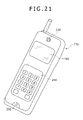
- FIG. 21 is a schematic view of an electronic apparatus as a portable terminal in the form of a portable telephone set to which the present invention is applied.
- liquid crystal display apparatus Before liquid crystal display apparatus according to preferred embodiments of the present invention are described, a basic configuration and functions of a liquid crystal display apparatus to which the present invention is applied are described in order to facilitate understanding of the present invention.
- FIG. 1 shows an example of a configuration of a liquid crystal display apparatus to which the present invention is applied.
- the liquid crystal display apparatus 1 shown includes an effective pixel region section 2 , a vertical driving circuit (VDRV) 3 and a horizontal driving circuit (HDRV) 4 .
- VDRV vertical driving circuit
- HDRV horizontal driving circuit
- the effective pixel region section 2 includes a plurality of pixel sections 2 PXL disposed in a matrix.
- Each pixel section 2 PXL includes a thin film transistor (TFT) 21 serving as a switching element, a liquid crystal cell LC 21 having a pixel electrode connected to the drain electrode or the source electrode of the TFT 21 , and a holding capacitor Cs 21 having an electrode connected to the drain electrode of the TFT 21 .
- TFT thin film transistor
- Scanning lines 5 - 1 to 5 - m extend in a pixel array direction along different rows while signal lines 6 - 1 to 6 - n extend in another pixel array direction along different columns of the pixel sections 2 PXL.
- the gate electrodes of the TFTs 21 of the pixel sections 2 PXL are connected to the same one of the scanning lines (gate lines) 5 - 1 to 5 - m in a unit of a row. Meanwhile, the source electrodes or the drain electrodes of the pixel sections 2 PXL are connected to the same one of the signal lines 6 - 1 to 6 - n in a unit of a column.
- a holding capacitor wiring line Cs is wired independently, and a holding capacitor Cs 21 is connected between the holding capacitor wiring line Cs and a connection electrode.
- a predetermined dc voltage is applied as a common voltage VCOM to the counter electrode of the liquid crystal cell LC 21 and the other electrode of the holding capacitor Cs 21 of the pixel section 2 PXL through a common wiring line 7 .
- a common voltage VCOM whose polarity reverses, for example, after each one horizontal scanning period ( 1 H) is applied to the counter electrode of the liquid crystal cell LC 21 and the other electrode of the holding capacitor Cs 21 of each pixel section 2 PXL.
- the scanning lines 5 - 1 to 5 - m are driven by the vertical driving circuit 3
- the signal lines 6 - 1 to 6 - n are driven by the horizontal driving circuit 4 .
- the TFT 21 is a switching element for selecting a pixel to be used for display and supplying a display signal to a display region of the pixel.
- the TFT 21 has, for example, such a bottom gate structure as shown in FIG. 2 or such a top gate structure as shown in FIG. 3 .
- the TFT 21 A of the bottom gate structure shown includes a gate electrode 203 formed on a transparent insulating substrate 201 , which may be a glass substrate, and covered with a gate insulating film 202 .
- the gate electrode 203 is connected to a scanning line (gate line) 5 such that a scanning signal is inputted from the scanning line 5 to the gate electrode 203 so that the TFT 21 A is turned on or off in response to the scanning signal.
- the gate electrode is formed by such a method as, for example, sputtering or the like of a metal or an alloy of molybdenum (Mo) or tantalum (Ta).
- the TFT 21 A includes a semiconductor film (channel formation region) 204 formed on the gate insulating film 202 and further includes a pair of n + diffused layers 205 and 206 formed across the semiconductor film 204 .
- An interlayer insulating film 207 is formed on the semiconductor film 204 , and another interlayer insulating film 208 is formed in such a manner as to cover the transparent insulating substrate 201 , gate insulating film 202 , n + diffused layers 205 and 206 and interlayer insulating film 207 .
- a source electrode 210 is connected to the n + diffused layer 205 through a contact hole 209 a formed in the interlayer insulating film 208 , and a drain electrode 211 is connected to the n + diffused layer 206 through another contact hole 209 b formed in the interlayer insulating film 208 .
- the source electrode 210 and the drain electrode 211 are formed, for example, by patterning aluminum (Al).
- a signal line 6 is connected to the source electrode 210 , and the drain electrode 211 is connected to the pixel region (pixel electrode) through a connection electrode not shown.
- the TFT 21 B of the top gate structure includes a semiconductor film (channel formation region) 222 formed on a transparent insulating substrate 221 which may be a glass substrate.
- the TFT 21 B further includes a pair of n + diffused layers 223 and 224 formed on the transparent insulating substrate 221 across the semiconductor film 222 .
- a gate insulating film 225 is formed in such a manner as to cover the semiconductor film 222 and the n + diffused layers 223 and 224
- a gate electrode 226 is formed on the gate insulating film 225 in an opposing relationship to the semiconductor film 222 .
- another interlayer insulating film 227 is formed so as to cover the transparent insulating substrate 221 , gate insulating film 225 and gate electrode 226 .
- a source electrode 229 is connected to the n + diffused layer 223 through a contact hole 228 a formed in the interlayer insulating film 227 and the gate insulating film 225 .
- a drain electrode 230 is connected to the n + diffused layer 224 through another contact hole 228 b formed in the interlayer insulating film 227 and the gate insulating film 225 .
- the vertical driving circuit 3 receives a vertical start signal VST, a vertical clock VCK and an enable signal ENB and performs processing of scanning in a vertical direction (column direction) for each one-field period to successively select the pixel sections 2 PXL connected to the scanning lines 5 - 1 to 5 - m in a unit of a row.
- scanning pulse SP 1 when a scanning pulse SP 1 is applied from the vertical driving circuit 3 to the scanning line 5 - 1 , then the pixels in the columns in the first row are selected, but when another scanning pulse SP 2 is applied to the scanning line 5 - 2 , the pixels in the columns in the second row are selected. Thereafter, scanning pulses SP 3 , . . . , SPm are successively applied to the scanning lines 5 - 3 , . . . , 5 - m in a similar manner, respectively.
- the horizontal driving circuit 4 receives a horizontal start pulse HST produced by a clock generator not shown for triggering horizontal scanning and horizontal clocks HCK and HCKX of the opposite phases to each other for serving as a reference to horizontal scanning to produce a sampling pulse. Further, the horizontal driving circuit 4 successively samples image data R (red), G (green) and B (blue) inputted thereto in response to the sampling pulse produced thereby and supplies the sampled data as data signals to be written into the pixel sections 2 PXL to the signal lines 6 - 1 to 6 - n.
- a horizontal start pulse HST produced by a clock generator not shown for triggering horizontal scanning and horizontal clocks HCK and HCKX of the opposite phases to each other for serving as a reference to horizontal scanning to produce a sampling pulse. Further, the horizontal driving circuit 4 successively samples image data R (red), G (green) and B (blue) inputted thereto in response to the sampling pulse produced thereby and supplies the sampled data as data signals to be written into the pixel sections 2 PXL to the signal lines
- the TFT 21 of the pixel sections 2 PXL is formed from a transistor of a semiconductor thin film of amorphous silicon (a-Si) or polycrystalline silicon.
- the liquid crystal display apparatus 1 having such a configuration as described above is formed as a liquid crystal display apparatus which is configured as an apparatus of the reflective and transmissive type and has a FFS (Fringe Field Switching) structure in order to assure a wide angular field of view.
- FFS Frringe Field Switching
- the effective pixel region section 2 has a particular structure described below in order that it can be driven by a single driving voltage for liquid crystal without employing a complicated driving method or driving circuit.
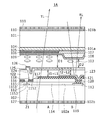
- FIG. 4 shows a layout of a liquid crystal display apparatus of the reflective and transmissive type according to a first embodiment of the present invention
- FIG. 5 shows a cross section of the liquid crystal display apparatus of the reflective and transmissive type.
- the liquid crystal display apparatus 1 A includes a liquid crystal layer 103 including a plurality of liquid crystal molecules and disposed between a first transparent substrate (upper transparent substrate) 101 and a second transparent substrate (lower transparent substrate) 102 .
- the liquid crystal layer 103 is held between and by the first transparent substrate 101 and the second transparent substrate 102 .
- the liquid crystal display apparatus 1 A has a transmission region A and a reflection region B formed in parallel to each other.
- the thickness (first liquid crystal thickness: first substrate gap) of the liquid crystal layer 103 in the transmission region A is set to D 1
- the thickness (second liquid crystal thickness: second substrate gap) of the liquid crystal layer 103 in the reflection region B is set to D 2 .
- the thicknesses D 1 and D 2 are set so as to satisfy a relationship D 1 >D 2 as seen in FIG. 5 .
- the first transparent substrate 101 and the second transparent substrate 102 are formed from a transparent insulating substrate of, for example, glass.
- the first transparent substrate 101 has a color filter 104 formed on a first face 101 a thereof which opposes to the liquid crystal layer 103 , and an orientation film 105 is formed on the color filter 104 .
- a non-phase difference film 106 and a phase difference film 107 are formed in parallel to each other on the orientation film 105 .
- the non-phase difference film 106 is formed on the transmission region A, and the phase difference film 107 is formed on the reflection region B.
- the non-phase difference film 106 is formed by selective exposure which may be UV exposure after, for example, a phase difference film is formed (applied).
- transmission light TL passes only once, and no phase difference adjustment is required. Therefore, the non-phase difference film 106 is disposed.
- phase difference film 107 is disposed.
- the reflection region B must selectively implement circularly polarized light. Therefore, the reflection region B requires a phase difference plate for establishing a circular polarization mode.
- phase difference plate in the form of a film for each pixel of the micron order on the outer side of the first transparent substrate 101 adjacent a light emerging side polarizing plate 111 if elongation and so forth of the film are taken into consideration.
- the phase difference film 107 is selectively formed in the liquid crystal cells to form the reflection region B as of the FFS type.
- phase difference film 107 in the reflection region B while the transmission region A passes linearly polarized light.
- the phase difference film 107 is formed on the first transparent substrate 101 to form an offset structure.
- the built-in phase difference film 107 applies retardation (circular polarization) of a 1 ⁇ 2 wavelength to vertically polarized light in the transmission region A.
- the retardation of the liquid crystal layer 103 in the reflection region B is a 1 ⁇ 4 wavelength.
- the reflection region B of the liquid crystal display apparatus 1 A light comes in from the polarizing plate 111 on the upper face of the liquid crystal display apparatus 1 A and is reflected by the reflecting film 121 in the liquid crystal panel. Thereafter, the light passes through the light emerging side polarizing plate 111 on the upper face of the apparatus gain. Consequently, the light can be recognized by an observer.
- the phases of the light which is to make dark display from a reflection region B and a transmission region A exhibit a phase difference of a 1 ⁇ 4 wavelength.
- a phase difference canceling portion (film) for shifting the wavelength of light through the reflection region B by a 1 ⁇ 4 wavelength is required.
- a flattening film 108 by which the gap D 2 of the liquid crystal layer 103 in the reflection region B can be adjusted is formed on the phase difference film 107 .
- a vertical orientation film (first orientation film) 109 is formed on the non-phase difference film 106 , phase difference film 107 and flattening film 108 .
- the light emerging side polarizing plate 111 is formed on a second face 101 b on the light emerging side of the first transparent substrate 101 with a pressure sensitive adhesive 110 interposed therebetween.
- a scanning wiring line 112 (corresponding to the scanning line (gate line) 5 of FIG. 1 ) which corresponds to the gate electrode of the TFT 21 is formed on the transmission region A side, and, for example, a VCOM common wiring line 113 (corresponding to the common wiring line 7 of FIG. 1 ) is formed on the reflection region B side.
- the scanning wiring line 112 may be formed by forming a film of a metal or an alloy, for example, of molybdenum (Mo) or tantalum (Ta).
- An insulating film 114 which functions as a gate insulating film is formed in such a manner as to cover the scanning wiring line 112 , VCOM common wiring line 113 and first face 102 a of the second transparent substrate 102 .
- n-type semiconductor layer 115 is formed in a region of the insulating film 114 opposing to the scanning wiring line (gate electrode) 112 .
- the semiconductor (thin film) layer 115 includes a source electrode portion (S) 1151 and a drain electrode portion (D) 1152 each in the form of a+diffusion layer, and a channel formation region 1153 .
- the semiconductor thin film layer 115 is formed from a thin film of low temperature polycrystalline silicon obtained, for example, by a CVD method or the like.
- the TFT 21 of FIG. 1 is formed from the scanning wiring line (gate electrode) 112 , semiconductor thin film layer 115 and so forth.
- the TFT 21 has a bottom gate structure.
- An interlayer insulating film 118 is formed on the semiconductor thin film layer 115 , signal wiring line 116 , conducting portion 117 and insulating film 114 .
- a contact hole 119 is formed in the insulating film 114 and the interlayer insulating film 118 on the VCOM common wiring line 113 such that it extends to the VCOM common wiring line 113 .
- a transparent counter electrode 120 made of, for example, ITO is formed on the interlayer insulating film 118 in the transmission region A and the reflection region B, in the contact hole 119 and on the VCOM common wiring line 113 in the contact hole 119 .
- the reflecting film 121 of metal having a high reflection factor is formed on the counter electrode 120 in the reflection region B.
- a transparent region side interlayer insulating film (first interlayer insulating film) 122 is formed on the interlayer insulating film 118 and the counter electrode 120 in the TFT regions and the transmission region A, and a reflection region side interlayer insulating film (second interlayer insulating film) 123 is formed on the reflecting film 121 in the reflection region B.
- the thickness L 1 of the first interlayer insulating film 122 and the thickness L 2 of the second interlayer insulating film 123 in the transmission region A are different from each other.
- the thickness L 1 and the thickness L 2 have a relationship of L 1 (t 1 )>L 2 (t 2 ).
- a contact hole 124 is formed in the interlayer insulating film 118 and the first interlayer insulating film 122 above the conducting portion 117 formed on the drain electrode portion 1152 of the semiconductor thin film layer 115 such that it extends to the conducting portion 117 .
- a transparent pixel electrode 125 made of, for example, ITO is formed on the first interlayer insulating film 122 and the second interlayer insulating film 123 , in the contact hole 124 and on the conducting portion 117 in the contact hole 124 .
- Pixel electrode blanked portions 1251 each in the form of a slit are formed as a fringe pattern on the pixel electrode 125 as seen in FIGS. 4 and 5 .
- a horizontal orientation film 126 having a predetermined rubbing axis is formed on the first interlayer insulating film 122 , second interlayer insulating film 123 and pixel electrode 125 .
- the polarizing plate 127 is formed on a second face 102 b side of the second transparent substrate 102 .
- L represents also electric lines of force (electric field strength)
- Vlcd is the driving voltage for the liquid crystal
- L the interlayer insulating film thickness or line distance
- D the liquid crystal thickness (gap)
- K the viscosity constant of the liquid crystal
- ⁇ lcd the relative dielectric constant of the liquid crystal.
- the gap is designed so as to be comparatively great, but if the electric lines of force are weak, then the gap is described so as to be comparatively small.
- the film thickness L 1 (t 1 ) of the first interlayer insulating film 122 is set to twice or more the thickness L 2 (t 2 ) of the second interlayer insulating film 123 so that the gap decreased by the reflection region B, that is, 1 ⁇ 2, is cancelled so that the driving voltages for the transmission region A and the reflection region B may be equal to each other.
- the first interlayer insulating film 122 and the second interlayer insulating film 123 have an equal relative dielectric constant.
- FIG. 6 illustrates a table of liquid crystal driving voltages and parameters used in the present embodiment.
- FIG. 7 illustrates a relationship between the interlayer insulation film and the liquid crystal driving voltage in the present embodiment.
- the axis of abscissa indicates the interlayer insulating film L
- the axis of abscissa indicates the liquid crystal driving voltage.
- a straight line denoted by ⁇ 1> illustrates a relationship between the interlayer insulating film and the liquid crystal driving voltage where the liquid crystal cell gap (liquid crystal thickness) D is 1 ⁇ m.
- Another straight line denoted by ⁇ 2> illustrates a relationship between the interlayer insulating film and the liquid crystal driving voltage where the liquid crystal cell gap (liquid crystal thickness) D is 2.25 ⁇ m.
- a further straight line denoted by ⁇ 3> illustrates a relationship between the interlayer insulating film and the liquid crystal driving voltage where the liquid crystal cell gap (liquid crystal thickness) D is 4.5 ⁇ m.
- a still further straight line denoted by ⁇ 4> illustrates a relationship between the interlayer insulating film and the liquid crystal driving voltage where the liquid crystal cell gap (liquid crystal thickness) D is 7 ⁇ m.
- the film thickness of the interlayer insulating film is indicated by L of the expression (1).
- liquid crystal display required time: ⁇ rise+ ⁇ fall ⁇ 33 ms is required.
- the necessary liquid crystal cell gap D is 1 ⁇ m or more.
- the interlayer insulating film is preferably equal to or greater than 0.15 ⁇ m.
- the condition in applications (driving voltage 3 V) to a mobile apparatus and a portable telephone set is 1/7(0.15) ⁇ L 2 /L 1 ⁇ 1.
- the interlayer insulating film thickness is not less than 0.15 ⁇ m but not more than 1 ⁇ m.
- the condition in an application (driving voltage 4.5 V) to a mobile apparatus or a notebook PC is 1 ⁇ 5 ⁇ L 2 /L 1 ⁇ 1.
- the interlayer insulating film thickness is not less than 0.2 ⁇ m but not more than 1 ⁇ m.
- the condition in an application (driving voltage 7.5 V) to a monitor PC is 1 ⁇ 3 ⁇ L 2 /L 1 ⁇ 1.
- the interlayer insulating film thickness is not less than 0.35 ⁇ m but not more than 1 ⁇ m.
- the condition in an application to a television set is 1 ⁇ 2 ⁇ L 2 /L 1 ⁇ 1.
- the interlayer insulating film thickness is more than 0.5 ⁇ m but less than 1 ⁇ m.
- the liquid crystal display apparatus 1 A having such a structure as described above has both of transmission and reflection functions of the FFS type.
- a single driving voltage can be used for both of transmission and reflection, the number of power supply voltages can be reduced and a level shifter circuit in the driving circuit can be configured in a simple circuit configuration.
- a complicated pixel layout in transmission and reflection regions of the pixel section can be simplified. Therefore, a pixel layout of a high transmission factor and a high reflection factor can be achieved.
- the driving circuits are handled with a simple power supply, the number of driving circuits can be reduced and the liquid crystal display apparatus can be fabricated at a reduced cost.
- FIG. 8 shows a liquid crystal display apparatus of the reflective and transmissive type according to a second embodiment of the present invention.
- the liquid crystal display apparatus 1 B of the second embodiment is a modification to the liquid crystal display apparatus 1 A of the first embodiment but is different in the following points.
- the liquid crystal display apparatus 1 B of the second embodiment is different in that the film thickness t 1 of the first interlayer insulating film 122 B between the pixel electrode 125 and the counter electrode 120 in the transmission region A and the film thickness t 2 of the second interlayer insulating film 123 B between the pixel electrode 125 and the counter electrode 120 in the reflection region B are set equal to each other so that the first interlayer insulating film 122 B and the second interlayer insulating film 123 B may have different relative dielectric constants from each other.
- the gap is determined relatively depending upon the transmission region A and the reflection region B, it is necessary to contrive the second transparent substrate 102 (TFT substrate) to adjust the driving voltages.
- the relative dielectric constant ⁇ 1 of the first interlayer insulating film 122 B is set to equal to or less than one half with respect to the relative dielectric constant ⁇ 2 of the second interlayer insulating film 123 B so that the gap reduced to one half in the reflection region is canceled to make the driving voltages for the transmission region A and the reflection region B equal to each other.
- the first interlayer insulating film 122 B and the second interlayer insulating film 123 B have an equal film thickness.
- interlayer insulating films 122 B and 123 B can be formed from an organic film of acrylic polyimide or the like.
- the liquid crystal display apparatus 1 B according to the present second embodiment has both of transmission and reflection functions of the FFS type and the IPS type similarly to the liquid crystal display apparatus 1 A of the first embodiment described hereinabove.
- a single driving voltage can be used for both of transmission and reflection, the number of power supply voltages can be reduced and a level shifter circuit in the driving circuit can be configured in a simple circuit configuration.
- a complicated pixel layout in transmission and reflection regions of the pixel section can be simplified. Therefore, a pixel layout of a high transmission factor and a high reflection factor can be achieved.
- the driving circuits are handled with a simple power supply, the number of driving circuits can be reduced and the liquid crystal display apparatus can be fabricated at a reduced cost.
- FIG. 9 shows a liquid crystal display apparatus of the reflective and transmissive type according to a third embodiment of the present invention.
- the liquid crystal display apparatus 1 C of the third embodiment is a modification to the liquid crystal display apparatus 1 B of the second embodiment but is different in the following points.
- the liquid crystal display apparatus 1 C of the third embodiment is different in that the liquid crystal layer thickness (gap thickness) D 1 in the transmission region A is set to equal or more than twice the liquid crystal layer thickness (gap thickness) D 2 in the reflection region B.
- the phase difference film 107 in the liquid crystal cells disposed in the reflection region B are located on the first transparent substrate 101 side.
- the reflection region B must selectively implement circularly polarized light. Therefore, the reflection region B requires a phase difference plate for establishing a circular polarization mode.
- phase difference plate in the form of a film for each pixel of the micron order on the outer side of the first transparent substrate 101 adjacent the light emerging side polarizing plate 111 if elongation and so forth of the film are taken into consideration.
- the phase difference film 107 is selectively formed in the liquid crystal cells to form the reflection region B as of the FFS type.
- phase difference film 107 in the reflection region B while the transmission region A passes linearly polarized light.
- the phase difference film 107 is formed on the first transparent substrate 101 to form an offset structure.
- the built-in phase difference film 107 applies retardation (circular polarization) of a 1 ⁇ 2 wavelength to vertically polarized light in the transmission region A.
- the retardation of the liquid crystal layer 103 in the reflection region B is a 1 ⁇ 4 wavelength.
- the phases of the light which is to make dark display from a reflection region B and a transmission region A exhibit a phase difference of a 1 ⁇ 4 wavelength.
- a phase difference canceling portion (film) for shifting the wavelength of light through the reflection region B by a 1 ⁇ 4 wavelength is required.
- FIG. 10 shows a liquid crystal display apparatus of the reflective and transmissive type according to a fourth embodiment of the present invention.
- the liquid crystal display apparatus 1 D of the fourth embodiment is a modification to the liquid crystal display apparatus 1 B of the second embodiment but is different in the following points.
- the liquid crystal display apparatus 1 D of the fourth embodiment is different in that the first interlayer insulating film 122 D in the transmission region A is formed so as to be covered with the second interlayer insulating film 123 D in the reflection region B and the relative dielectric constant ⁇ 1 in the transmission region A and the relative dielectric constant ⁇ 2 are made different from each other so as to satisfy ⁇ 1 ⁇ 2 ⁇ 6 ⁇ 1 or ⁇ 2 ⁇ 2 ⁇ 1
- the thickness of the interlayer insulating film in the transmission region A is t 1 +t 2
- the thickness of the interlayer insulating film in the reflection region B is t 2 . Consequently, the relationship of t 1 +t 2 >t 2 is satisfied.
- FIG. 11 shows a liquid crystal display apparatus of the reflective and transmissive type according to a fifth embodiment of the present invention.
- the liquid crystal display apparatus 1 E of the fifth embodiment is a modification to the liquid crystal display apparatus 1 B of the second embodiment but is different in the following points.
- the liquid crystal display apparatus 1 E of the fifth embodiment is different in that the first interlayer insulating film 122 E in the transmission region A is formed so as to cover the second interlayer insulating film 123 E in the reflection region B and the relative dielectric constant ⁇ 1 in the transmission region A and the relative dielectric constant ⁇ 2 in the reflection region B are made different from each other so as to satisfy the requirement of ⁇ 1 ⁇ 2 ⁇ 6 ⁇ 1 or ⁇ 2 ⁇ 2 ⁇ 1 .
- the thickness of the interlayer insulating film in the transmission region A is t 1 and the thickness of the interlayer insulating film in the reflection region B is t 1 +t 2 . Therefore, the relationship of t 1 ⁇ t 1 +t 2 is satisfied.
- FIG. 12 shows a liquid crystal display apparatus of the reflective and transmissive type according to a sixth embodiment of the present invention.
- the liquid crystal display apparatus 1 F of the sixth embodiment is a modification to the liquid crystal display apparatus 1 B of the second embodiment but is different in the following points.
- the liquid crystal display apparatus 1 F of the sixth embodiment is different in that the relative dielectric constant ⁇ 1 of the first interlayer insulating film 122 F is different from the relative dielectric constant ⁇ 2 of the second interlayer insulating film 123 F and besides the first interlayer insulating film 122 F and the second interlayer insulating film 123 F have different film thicknesses from each other.
- the interlayer insulating film in the transmission region A and the reflection region B have different relative dielectric constants from each other.
- the first interlayer insulating film 122 F in the transmission region A and the second interlayer insulating film 123 F in the reflection region B which have different relative dielectric constants from each other are formed (t 1 >t 2 ).
- the relative dielectric constant ⁇ 1 of the first interlayer insulating film 122 F in the transmission region A and the relative dielectric constant ⁇ 2 of the second interlayer insulating film 123 F in the reflection region B are made different from each other.
- the first interlayer insulating film 122 F is made of SiN and has a relative dielectric constant of 7.5 while the second interlayer insulating film 123 F is made of SiO 2 and has another relative dielectric constant of 3.9.
- the film thickness of the first interlayer insulating film 122 F is 1 ⁇ m
- the film thickness of the second interlayer insulating film 123 F is 0.7 ⁇ m.
- the driving voltage in the transmission region A having the first interlayer insulating film 122 F is 3.34 V while the driving voltage in the reflection region B having the second interlayer insulating film 123 F is 3.24 V. Consequently, the driving voltages for transmission and reception can be made substantially equal to each other.
- FIGS. 14 and 15 show a liquid crystal display apparatus of the reflective and transmissive type according to a seventh embodiment of the present invention.
- the liquid crystal display apparatus 1 G of the seventh embodiment is a modification to the liquid crystal display apparatus 1 F of the sixth embodiment but is different in the following points.
- the liquid crystal display apparatus 1 G of the seventh embodiment is different in that the film thickness t 2 of the second interlayer insulating film 123 G is set greater than the film thickness t 1 of the first interlayer insulating film 122 G to form the gap D 2 in the reflection region B.
- the flattening film on the first transparent substrate 101 side is unnecessary.
- the film thickness t 2 of the second interlayer insulating film 123 G in the reflection region B is set greater than the film thickness t 1 of the first interlayer insulating film 122 G in the transmission region A and besides the effective pixel region section 2 in the reflection region B is used so as to serve also as an offset portion for the multi-gaps in the reflection region B.
- the relative dielectric constant ⁇ 1 of the first interlayer insulating film 122 G in the transmission region A is made different from the relative dielectric constant ⁇ 2 of the second interlayer insulating film 123 G in the reflection region B.
- the effective pixel region section 2 is formed as an offset portion for obtaining multi-gaps in the reflection region B.
- the first interlayer insulating film 122 G is made of SiO 2 and has a relative dielectric constant of 3.9 while the second interlayer insulating film 123 G is made of TaO 2 and has another relative dielectric constant of 22.
- the first interlayer insulating film 122 G is 0.5 ⁇ m
- the second interlayer insulating film 123 G is 1 ⁇ m.
- the driving voltage in the transmission region A having the first interlayer insulating film 122 G becomes 3.49 V
- the driving voltage in the reflection region B having the second interlayer insulating film 123 G becomes 4.39. Consequently, the driving voltages for transmission and reflection can be made substantially equal to each other.
- the liquid crystal layer thickness (substrate gap) D 1 in the transmission region A can be set to 3 ⁇ m
- the gap (substrate gap) D 2 in the reflection region B can be set to 2 ⁇ m. Consequently, an offset portion can be formed from the interlayer insulating film in the reflection region B.
- the present invention can be applied also where the material of the second interlayer insulating film 123 G in the reflection region B is SIN.
- the counter electrode overhangs (has an overlapping relationship with) the signal line and the gate line in transmissive and reflective type liquid crystal display as seen in FIG. 14 .
- the counter electrode 120 made of ITO or the like is disposed immediately above the signal wiring line 116 and the scanning wiring line (gate line) 112 , jumping of a voltage variation from the signal wiring line 116 and the scanning wiring line (gate line) 112 into the counter electrode 120 can be prevented. Consequently, the variation at the signal wiring line 116 to the pixel electrode 125 disposed above the counter electrode 120 and the pixel electrode (ITO) 125 from the scanning wiring line (gate line) 112 by jumping in of the voltage variation can be suppressed. As a result, deterioration of the picture quality by flickering by horizontal and vertical crosstalk which appears in the liquid crystal display apparatus can be prevented.
- FIGS. 17 and 18 show a liquid crystal display apparatus of the reflective and transmissive type according to an eighth embodiment of the present invention.
- the liquid crystal display apparatus 1 H of the eighth embodiment is characterized in that, in transmission liquid crystal display and transmission and reflection liquid crystal display, a counter electrode overhangs (has an overlapping relationship with) a signal line and a gate line.
- the liquid crystal display apparatus 1 H of the eighth embodiment is a modification to the liquid crystal display apparatus 1 A of the first embodiment but is different in the following points.
- an orientation film 105 is formed on the color filter 104 .
- the reflecting film 121 is not formed and no multi-gap structure is provided.
- the counter electrode 120 made of ITO or the like is disposed immediately above the signal wiring line 116 and the scanning wiring line (gate line) 112 . Therefore, jumping of a voltage variation from the signal wiring line 116 and the scanning wiring line (gate line) 112 into the counter electrode 120 can be prevented. Consequently, the variation at the signal wiring line 116 to the pixel electrode 125 disposed above the counter electrode 120 and the pixel electrode (ITO) 125 from the scanning wiring line (gate line) 112 by jumping in of the voltage variation can be suppressed. As a result, deterioration of the picture quality by flickering by horizontal and vertical crosstalk which appears in the liquid crystal display apparatus can be prevented.
- FIGS. 19 and 20 show a liquid crystal display apparatus of the reflective and transmissive type according to a ninth embodiment of the present invention.
- the liquid crystal display apparatus 1 I of the ninth embodiment is a modification to the liquid crystal display apparatus 1 A of the first embodiment but is different in that it is formed not as that of the FFS type but as that of the IPS type.
- a flattening film 108 I is formed on the color filter 104 , and a non-phase difference film 106 and a phase difference film 107 are formed in parallel on the flattening film 108 I. Further, an orientation film 109 is formed on the non-phase difference film 106 and the phase difference film 107 .
- a reflecting film 121 is formed on the insulating film 114 in the reflection region B, and a counter electrode 120 I and a pixel electrode 125 I are formed in a comb-like shape on the first interlayer insulating film 122 I and the second interlayer insulating film 123 I such that they are opposed to each other.
- the line distance between the pixel electrode 125 I and the counter electrode 120 I is made different between the transmission region A and the reflection region B.
- the thickness L 1 of the first interlayer insulating film 122 I and the thickness L 2 of the second interlayer insulating film 123 I satisfy a relationship of L 2 ⁇ 1 ⁇ 2 ⁇ L 1 .
- a liquid crystal display apparatus can be formed which has both functions of transmission and reception while it is of the IPS type.
- a single driving voltage can be used for both of transmission and reflection, the number of power supply voltages can be reduced and a level shifter circuit in the driving circuit can be configured in a simple circuit configuration.
- a complicated pixel layout in transmission and reflection regions of the pixel section can be simplified. Therefore, a pixel layout of a high transmission factor and a high reflection factor can be achieved.
- the driving circuits are handled with a simple power supply, the number of driving circuits can be reduced and the liquid crystal display apparatus can be fabricated at a reduced cost.
- an active matrix type display apparatus represented by the active matrix type liquid crystal display apparatus according to the embodiments described above is used as a display apparatus for OA apparatus such as a personal computer or a word processor and a television receiver. Further, the active matrix type display apparatus can be suitably used as a display section for a portable telephone set or a PDA with regard to which miniaturization and compaction particularly of an apparatus body are being proceeded.
- FIG. 21 shows an outline of a configuration of an electronic apparatus such as, for example, a portable telephone set to which any of the liquid crystal display apparatus according to the embodiments described hereinabove can be applied.
- the portable telephone set 200 shown includes a speaker section 220 , a display section 260 , an operation section 240 and a microphone section 250 disposed in order from above on a front face of an apparatus housing 270 .
- a liquid crystal display apparatus is used for the display section 260 , and any of the active matrix type liquid crystal display apparatus according to the embodiments of the present invention described hereinabove is applied as the liquid crystal display apparatus.
- the active matrix type liquid crystal display apparatus according to any of the embodiments described hereinabove is used as the display section 260 in the portable terminal such as the portable telephone set
- the dispersion of the output frequency of an oscillator which has some frequency dispersion can be suppressed so as to be within a predetermined certain guaranteed range.
- a circuit block which is independent and does not rely upon the voltage or the frequency of an interface can be configured and controlled. Therefore, a circuit-integrated type liquid crystal display apparatus compatible with a low voltage and a high frequency of the interface can be implemented.
Abstract
Description
Vlcd=π·L/D√{square root over ( )}(K/∈lcd) (1)
where Vlcd is the driving voltage for the liquid crystal, L the interlayer insulating film thickness or line distance, D the liquid crystal thickness (gap), K the viscosity constant of the liquid crystal, and ∈lcd the relative dielectric constant of the liquid crystal.
Vlcd=n·L/D√{square root over ( )}(K/∈lcd) (1)
where Vlcd is the driving voltage for the liquid crystal, L the interlayer insulating film thickness or line distance, D the liquid crystal thickness (gap), K the viscosity constant of the liquid crystal, and ∈lcd the relative dielectric constant of the liquid crystal.
Claims (9)
Applications Claiming Priority (2)
| Application Number | Priority Date | Filing Date | Title |
|---|---|---|---|
| JP2006-241355 | 2006-09-06 | ||
| JP2006241355A JP4285516B2 (en) | 2006-09-06 | 2006-09-06 | Liquid crystal display device and electronic device |
Publications (2)
| Publication Number | Publication Date |
|---|---|
| US20080055526A1 US20080055526A1 (en) | 2008-03-06 |
| US8421968B2 true US8421968B2 (en) | 2013-04-16 |
Family
ID=39150979
Family Applications (1)
| Application Number | Title | Priority Date | Filing Date |
|---|---|---|---|
| US11/850,323 Expired - Fee Related US8421968B2 (en) | 2006-09-06 | 2007-09-05 | Liquid crystal display apparatus and electronic apparatus |
Country Status (5)
| Country | Link |
|---|---|
| US (1) | US8421968B2 (en) |
| JP (1) | JP4285516B2 (en) |
| KR (1) | KR101456902B1 (en) |
| CN (1) | CN101140399B (en) |
| TW (1) | TWI395010B (en) |
Cited By (1)
| Publication number | Priority date | Publication date | Assignee | Title |
|---|---|---|---|---|
| US20120236243A1 (en) * | 2005-09-15 | 2012-09-20 | Ong Hiap L | Liquid Crystal Displays Having Pixels with Embedded Fringe Field Amplifiers |
Families Citing this family (20)
| Publication number | Priority date | Publication date | Assignee | Title |
|---|---|---|---|---|
| KR101215027B1 (en) * | 2005-12-21 | 2012-12-26 | 삼성디스플레이 주식회사 | Transreflective liquid crystal display and driving method thereof |
| JP2008170501A (en) * | 2007-01-09 | 2008-07-24 | Hitachi Displays Ltd | Liquid crystal display device and its manufacturing method |
| KR101427584B1 (en) * | 2008-01-22 | 2014-08-08 | 삼성디스플레이 주식회사 | Display device |
| JP4618336B2 (en) * | 2008-06-16 | 2011-01-26 | ソニー株式会社 | Liquid crystal display device |
| JP5207947B2 (en) * | 2008-12-16 | 2013-06-12 | 株式会社ジャパンディスプレイウェスト | Liquid crystal display device and manufacturing method thereof |
| CN102422206A (en) * | 2009-03-09 | 2012-04-18 | 奇像素公司 | Normally black transflective liquid crystal displays |
| US8698716B2 (en) | 2010-05-18 | 2014-04-15 | Pixel Qi Corporation | Low power consumption transflective liquid crystal displays |
| US8830426B2 (en) | 2010-11-17 | 2014-09-09 | Pixel Qi Corporation | Color shift reduction in transflective liquid crystal displays |
| WO2013168566A1 (en) * | 2012-05-10 | 2013-11-14 | シャープ株式会社 | Liquid crystal display device |
| JP6072522B2 (en) * | 2012-11-29 | 2017-02-01 | 三菱電機株式会社 | Liquid crystal display panel and manufacturing method thereof |
| CN103268041B (en) * | 2013-05-17 | 2015-11-25 | 京东方科技集团股份有限公司 | Display panels and driving method thereof |
| CN103984141B (en) * | 2014-05-04 | 2015-05-06 | 京东方科技集团股份有限公司 | Liquid crystal display (LCD) panel and LCD device |
| CN104730784B (en) * | 2015-04-14 | 2017-12-08 | 京东方科技集团股份有限公司 | Array base palte and its manufacture method, display panel and display device |
| KR102390441B1 (en) * | 2015-10-15 | 2022-04-26 | 삼성디스플레이 주식회사 | Organic light emitting display device |
| JP6651859B2 (en) * | 2016-01-12 | 2020-02-19 | 凸版印刷株式会社 | Thin film transistor array and reflective display device |
| CN107861295A (en) * | 2017-11-24 | 2018-03-30 | 深圳市华星光电技术有限公司 | A kind of array base palte and preparation method thereof, display panel |
| JP7109924B2 (en) * | 2018-01-12 | 2022-08-01 | 株式会社ジャパンディスプレイ | Display device |
| US11428982B2 (en) * | 2018-07-04 | 2022-08-30 | Sony Corporation | Electrode structure, method for manufacturing electrode structure, liquid crystal display element, method for driving liquid crystal display element, and electronic equipment |
| CN109884833B (en) * | 2019-05-09 | 2019-09-03 | 南京中电熊猫平板显示科技有限公司 | A kind of Demultiplexing circuitry, liquid crystal display device and pixel compensation method |
| KR102361863B1 (en) | 2021-07-15 | 2022-02-14 | 주식회사 비츠로브이엠 | Gate valve with gas prevention stopper |
Citations (19)
| Publication number | Priority date | Publication date | Assignee | Title |
|---|---|---|---|---|
| JPH0990424A (en) | 1995-09-19 | 1997-04-04 | Sony Corp | Thin-film semiconductor device |
| JPH10213808A (en) | 1997-01-31 | 1998-08-11 | Sharp Corp | Liquid crystal display device |
| JP2001042366A (en) | 1999-06-29 | 2001-02-16 | Hyundai Electronics Ind Co Ltd | Reflection type fringe field switching mode liquid crystal display device |
| US20010052948A1 (en) * | 1997-12-26 | 2001-12-20 | Sharp Kabushiki Kaisha | Liquid crystal display |
| JP2002229032A (en) | 2000-12-05 | 2002-08-14 | Hyundai Display Technology Inc | Reflection type fringe-field switching mode liquid crystal display |
| WO2005006068A1 (en) | 2003-07-14 | 2005-01-20 | Hitachi Displays, Ltd. | Display unit |
| US20050128389A1 (en) * | 2003-12-12 | 2005-06-16 | Innolux Display Corp. | Transflective fringe field switching liquid crystal display |
| JP2005524115A (en) | 2002-04-30 | 2005-08-11 | ユニバーシティ・オブ・セントラル・フロリダ | Transflective liquid crystal display with partial switching function |
| US20050190324A1 (en) * | 2004-02-27 | 2005-09-01 | Innolux Display Corp. | In-plane field type transflective liquid crystal display device |
| JP2005338264A (en) | 2004-05-25 | 2005-12-08 | Hitachi Displays Ltd | Liquid crystal display |
| JP2006003808A (en) | 2004-06-21 | 2006-01-05 | Seiko Epson Corp | Liquid crystal apparatus and electronic device |
| JP2006003908A (en) | 2005-07-06 | 2006-01-05 | Sumitomo Chemical Co Ltd | Method of manufacturing phase difference film |
| JP2006071977A (en) | 2004-09-02 | 2006-03-16 | Sony Corp | Liquid crystal display device and method for manufacturing the same |
| JP2006091930A (en) | 1997-12-26 | 2006-04-06 | Sharp Corp | Liquid crystal display |
| JP2006276110A (en) | 2005-03-28 | 2006-10-12 | Sanyo Epson Imaging Devices Corp | Liquid crystal device and electronic apparatus |
| US20060256268A1 (en) * | 2005-05-11 | 2006-11-16 | Boe Hydis Technology Co., Ltd. | Fringe field switching mode transflective liquid crystal display |
| US20060279677A1 (en) * | 2005-06-09 | 2006-12-14 | Sanyo Epson Imaging Devices Corporation | Liquid crystal device and electronic apparatus |
| US20070146591A1 (en) * | 2005-12-05 | 2007-06-28 | Semiconductor Energy Laboratory Co., Ltd. | Liquid crystal display device |
| US20070263148A1 (en) * | 2006-05-15 | 2007-11-15 | Masahiro Teramoto | Liquid Crystal Display Device |
Family Cites Families (2)
| Publication number | Priority date | Publication date | Assignee | Title |
|---|---|---|---|---|
| TWI300148B (en) * | 2004-01-09 | 2008-08-21 | Innolux Display Corp | Liquid crystal display device |
| KR100713892B1 (en) * | 2005-02-17 | 2007-05-04 | 비오이 하이디스 테크놀로지 주식회사 | Transflective fringe field switching mode liquid crystal display |
-
2006
- 2006-09-06 JP JP2006241355A patent/JP4285516B2/en active Active
-
2007
- 2007-07-26 TW TW096127327A patent/TWI395010B/en not_active IP Right Cessation
- 2007-08-29 KR KR1020070087010A patent/KR101456902B1/en not_active IP Right Cessation
- 2007-09-05 US US11/850,323 patent/US8421968B2/en not_active Expired - Fee Related
- 2007-09-06 CN CN2007101487081A patent/CN101140399B/en not_active Expired - Fee Related
Patent Citations (20)
| Publication number | Priority date | Publication date | Assignee | Title |
|---|---|---|---|---|
| JPH0990424A (en) | 1995-09-19 | 1997-04-04 | Sony Corp | Thin-film semiconductor device |
| JPH10213808A (en) | 1997-01-31 | 1998-08-11 | Sharp Corp | Liquid crystal display device |
| JP2006091930A (en) | 1997-12-26 | 2006-04-06 | Sharp Corp | Liquid crystal display |
| US20010052948A1 (en) * | 1997-12-26 | 2001-12-20 | Sharp Kabushiki Kaisha | Liquid crystal display |
| JP2001042366A (en) | 1999-06-29 | 2001-02-16 | Hyundai Electronics Ind Co Ltd | Reflection type fringe field switching mode liquid crystal display device |
| JP2002229032A (en) | 2000-12-05 | 2002-08-14 | Hyundai Display Technology Inc | Reflection type fringe-field switching mode liquid crystal display |
| JP2005524115A (en) | 2002-04-30 | 2005-08-11 | ユニバーシティ・オブ・セントラル・フロリダ | Transflective liquid crystal display with partial switching function |
| WO2005006068A1 (en) | 2003-07-14 | 2005-01-20 | Hitachi Displays, Ltd. | Display unit |
| US20050128389A1 (en) * | 2003-12-12 | 2005-06-16 | Innolux Display Corp. | Transflective fringe field switching liquid crystal display |
| US20050190324A1 (en) * | 2004-02-27 | 2005-09-01 | Innolux Display Corp. | In-plane field type transflective liquid crystal display device |
| JP2005338264A (en) | 2004-05-25 | 2005-12-08 | Hitachi Displays Ltd | Liquid crystal display |
| JP2006003808A (en) | 2004-06-21 | 2006-01-05 | Seiko Epson Corp | Liquid crystal apparatus and electronic device |
| JP2006071977A (en) | 2004-09-02 | 2006-03-16 | Sony Corp | Liquid crystal display device and method for manufacturing the same |
| JP2006276110A (en) | 2005-03-28 | 2006-10-12 | Sanyo Epson Imaging Devices Corp | Liquid crystal device and electronic apparatus |
| US20060256268A1 (en) * | 2005-05-11 | 2006-11-16 | Boe Hydis Technology Co., Ltd. | Fringe field switching mode transflective liquid crystal display |
| US20060279677A1 (en) * | 2005-06-09 | 2006-12-14 | Sanyo Epson Imaging Devices Corporation | Liquid crystal device and electronic apparatus |
| JP2007017943A (en) | 2005-06-09 | 2007-01-25 | Sanyo Epson Imaging Devices Corp | Liquid crystal device and electronic apparatus |
| JP2006003908A (en) | 2005-07-06 | 2006-01-05 | Sumitomo Chemical Co Ltd | Method of manufacturing phase difference film |
| US20070146591A1 (en) * | 2005-12-05 | 2007-06-28 | Semiconductor Energy Laboratory Co., Ltd. | Liquid crystal display device |
| US20070263148A1 (en) * | 2006-05-15 | 2007-11-15 | Masahiro Teramoto | Liquid Crystal Display Device |
Non-Patent Citations (2)
| Title |
|---|
| Japanese Office Action dated Jul. 1, 2008 for Application No. 2006-241355. |
| Japanese Office Action issued on May 10, 2011 in connection with counterpart JP Application No. 2008-223165. |
Cited By (2)
| Publication number | Priority date | Publication date | Assignee | Title |
|---|---|---|---|---|
| US20120236243A1 (en) * | 2005-09-15 | 2012-09-20 | Ong Hiap L | Liquid Crystal Displays Having Pixels with Embedded Fringe Field Amplifiers |
| US9443483B2 (en) * | 2005-09-15 | 2016-09-13 | Hiap L. Ong and Kyoritsu Optronics, Co., Ltd. | Liquid crystal displays having pixels with embedded fringe field amplifiers |
Also Published As
| Publication number | Publication date |
|---|---|
| CN101140399A (en) | 2008-03-12 |
| TWI395010B (en) | 2013-05-01 |
| TW200823536A (en) | 2008-06-01 |
| JP2008064947A (en) | 2008-03-21 |
| US20080055526A1 (en) | 2008-03-06 |
| JP4285516B2 (en) | 2009-06-24 |
| KR101456902B1 (en) | 2014-10-31 |
| KR20080022502A (en) | 2008-03-11 |
| CN101140399B (en) | 2010-06-23 |
Similar Documents
| Publication | Publication Date | Title |
|---|---|---|
| US8421968B2 (en) | Liquid crystal display apparatus and electronic apparatus | |
| US10151952B2 (en) | Display device and electronic apparatus | |
| KR100816145B1 (en) | Liquid crystal device and electronic apparatus | |
| JP4111203B2 (en) | Liquid crystal device and electronic device | |
| US7321409B2 (en) | Transflective liquid crystal device and electronic apparatus using the same | |
| US20090128757A1 (en) | Liquid crystal device and electronic apparatus | |
| US20080111779A1 (en) | Liquid-crystal display, method for producing liquid-crystal display, and electronic device | |
| US7663716B2 (en) | Liquid crystal display device and electronic apparatus | |
| KR20080023164A (en) | Liquid crystal display device and eletronic equipment | |
| WO2004017132A1 (en) | A ocb mode liquid crystal display and a driving method of the same | |
| US7483099B2 (en) | Liquid crystal device and electronic apparatus | |
| US7907240B2 (en) | Transflective liquid crystal device and electronic apparatus having a liquid crystal layer of varying thickness | |
| JP4887745B2 (en) | Liquid crystal device and electronic device | |
| JP2003270627A (en) | Transflective liquid crystal device and electronic device using the same | |
| US20090091679A1 (en) | Liquid crystal display | |
| JP2009075421A (en) | Liquid crystal device and electronic equipment | |
| US20080186420A1 (en) | Liquid crystal display device and electronic apparatus including the same | |
| JP5271639B2 (en) | Liquid crystal display device and electronic device | |
| JP4858081B2 (en) | Electro-optical device and manufacturing method thereof | |
| EP1890185A1 (en) | Transflective pixel structure in lcd panel and method for fabricating the same | |
| JP2008197129A (en) | Liquid crystal device and electronic apparatus | |
| JP2008033371A (en) | Transflective liquid crystal device and electronic equipment using the same | |
| KR20060120884A (en) | Liquid crystal display |
Legal Events
| Date | Code | Title | Description |
|---|---|---|---|
| AS | Assignment |
Owner name: SONY CORPORATION, JAPAN Free format text: ASSIGNMENT OF ASSIGNORS INTEREST;ASSIGNOR:INO, MASUMITSU;REEL/FRAME:019788/0899 Effective date: 20070720 |
|
| STCF | Information on status: patent grant |
Free format text: PATENTED CASE |
|
| AS | Assignment |
Owner name: JAPAN DISPLAY WEST INC., JAPAN Free format text: ASSIGNMENT OF ASSIGNORS INTEREST;ASSIGNOR:SONY CORPORATION;REEL/FRAME:030192/0347 Effective date: 20130325 |
|
| FEPP | Fee payment procedure |
Free format text: PAYOR NUMBER ASSIGNED (ORIGINAL EVENT CODE: ASPN); ENTITY STATUS OF PATENT OWNER: LARGE ENTITY |
|
| FPAY | Fee payment |
Year of fee payment: 4 |
|
| FEPP | Fee payment procedure |
Free format text: MAINTENANCE FEE REMINDER MAILED (ORIGINAL EVENT CODE: REM.); ENTITY STATUS OF PATENT OWNER: LARGE ENTITY |
|
| LAPS | Lapse for failure to pay maintenance fees |
Free format text: PATENT EXPIRED FOR FAILURE TO PAY MAINTENANCE FEES (ORIGINAL EVENT CODE: EXP.); ENTITY STATUS OF PATENT OWNER: LARGE ENTITY |
|
| STCH | Information on status: patent discontinuation |
Free format text: PATENT EXPIRED DUE TO NONPAYMENT OF MAINTENANCE FEES UNDER 37 CFR 1.362 |
|
| FP | Lapsed due to failure to pay maintenance fee |
Effective date: 20210416 |