US8409902B1 - Ablation of film stacks in solar cell fabrication processes - Google Patents
Ablation of film stacks in solar cell fabrication processes Download PDFInfo
- Publication number
- US8409902B1 US8409902B1 US13/486,095 US201213486095A US8409902B1 US 8409902 B1 US8409902 B1 US 8409902B1 US 201213486095 A US201213486095 A US 201213486095A US 8409902 B1 US8409902 B1 US 8409902B1
- Authority
- US
- United States
- Prior art keywords
- film
- laser
- pulse
- solar cell
- laser pulse
- Prior art date
- Legal status (The legal status is an assumption and is not a legal conclusion. Google has not performed a legal analysis and makes no representation as to the accuracy of the status listed.)
- Active
Links
- 238000000034 method Methods 0.000 title claims description 28
- 238000004519 manufacturing process Methods 0.000 title claims description 9
- 238000002679 ablation Methods 0.000 title abstract description 28
- 238000009792 diffusion process Methods 0.000 claims description 16
- 239000000758 substrate Substances 0.000 claims description 11
- 229910052581 Si3N4 Inorganic materials 0.000 claims description 10
- 229910052710 silicon Inorganic materials 0.000 claims description 10
- 239000010703 silicon Substances 0.000 claims description 10
- HQVNEWCFYHHQES-UHFFFAOYSA-N silicon nitride Chemical compound N12[Si]34N5[Si]62N3[Si]51N64 HQVNEWCFYHHQES-UHFFFAOYSA-N 0.000 claims description 10
- XUIMIQQOPSSXEZ-UHFFFAOYSA-N Silicon Chemical compound [Si] XUIMIQQOPSSXEZ-UHFFFAOYSA-N 0.000 claims description 9
- 238000010304 firing Methods 0.000 claims description 6
- 239000000463 material Substances 0.000 abstract description 10
- 239000010408 film Substances 0.000 description 58
- 229910021417 amorphous silicon Inorganic materials 0.000 description 12
- 239000004065 semiconductor Substances 0.000 description 8
- 239000002184 metal Substances 0.000 description 5
- 229910021420 polycrystalline silicon Inorganic materials 0.000 description 5
- 229920005591 polysilicon Polymers 0.000 description 5
- 238000012360 testing method Methods 0.000 description 5
- 239000010409 thin film Substances 0.000 description 5
- 230000005855 radiation Effects 0.000 description 3
- 230000006798 recombination Effects 0.000 description 3
- 238000005215 recombination Methods 0.000 description 3
- VYPSYNLAJGMNEJ-UHFFFAOYSA-N Silicium dioxide Chemical compound O=[Si]=O VYPSYNLAJGMNEJ-UHFFFAOYSA-N 0.000 description 2
- 238000010521 absorption reaction Methods 0.000 description 2
- 230000001939 inductive effect Effects 0.000 description 2
- 230000003287 optical effect Effects 0.000 description 2
- 238000012545 processing Methods 0.000 description 2
- 230000003667 anti-reflective effect Effects 0.000 description 1
- 230000009286 beneficial effect Effects 0.000 description 1
- 230000015572 biosynthetic process Effects 0.000 description 1
- 230000015556 catabolic process Effects 0.000 description 1
- 230000007547 defect Effects 0.000 description 1
- 238000006731 degradation reaction Methods 0.000 description 1
- 238000011161 development Methods 0.000 description 1
- 238000005553 drilling Methods 0.000 description 1
- 238000005516 engineering process Methods 0.000 description 1
- 238000000608 laser ablation Methods 0.000 description 1
- 238000002161 passivation Methods 0.000 description 1
- 230000037361 pathway Effects 0.000 description 1
- 230000010287 polarization Effects 0.000 description 1
- 238000011160 research Methods 0.000 description 1
- 235000012239 silicon dioxide Nutrition 0.000 description 1
- 239000000377 silicon dioxide Substances 0.000 description 1
Images


Classifications
-
- B—PERFORMING OPERATIONS; TRANSPORTING
- B23—MACHINE TOOLS; METAL-WORKING NOT OTHERWISE PROVIDED FOR
- B23K—SOLDERING OR UNSOLDERING; WELDING; CLADDING OR PLATING BY SOLDERING OR WELDING; CUTTING BY APPLYING HEAT LOCALLY, e.g. FLAME CUTTING; WORKING BY LASER BEAM
- B23K26/00—Working by laser beam, e.g. welding, cutting or boring
- B23K26/02—Positioning or observing the workpiece, e.g. with respect to the point of impact; Aligning, aiming or focusing the laser beam
- B23K26/06—Shaping the laser beam, e.g. by masks or multi-focusing
- B23K26/062—Shaping the laser beam, e.g. by masks or multi-focusing by direct control of the laser beam
- B23K26/0622—Shaping the laser beam, e.g. by masks or multi-focusing by direct control of the laser beam by shaping pulses
-
- B—PERFORMING OPERATIONS; TRANSPORTING
- B23—MACHINE TOOLS; METAL-WORKING NOT OTHERWISE PROVIDED FOR
- B23K—SOLDERING OR UNSOLDERING; WELDING; CLADDING OR PLATING BY SOLDERING OR WELDING; CUTTING BY APPLYING HEAT LOCALLY, e.g. FLAME CUTTING; WORKING BY LASER BEAM
- B23K26/00—Working by laser beam, e.g. welding, cutting or boring
- B23K26/36—Removing material
- B23K26/38—Removing material by boring or cutting
- B23K26/382—Removing material by boring or cutting by boring
- B23K26/384—Removing material by boring or cutting by boring of specially shaped holes
-
- B—PERFORMING OPERATIONS; TRANSPORTING
- B23—MACHINE TOOLS; METAL-WORKING NOT OTHERWISE PROVIDED FOR
- B23K—SOLDERING OR UNSOLDERING; WELDING; CLADDING OR PLATING BY SOLDERING OR WELDING; CUTTING BY APPLYING HEAT LOCALLY, e.g. FLAME CUTTING; WORKING BY LASER BEAM
- B23K26/00—Working by laser beam, e.g. welding, cutting or boring
- B23K26/36—Removing material
- B23K26/40—Removing material taking account of the properties of the material involved
- B23K26/402—Removing material taking account of the properties of the material involved involving non-metallic material, e.g. isolators
-
- H—ELECTRICITY
- H01—ELECTRIC ELEMENTS
- H01L—SEMICONDUCTOR DEVICES NOT COVERED BY CLASS H10
- H01L31/00—Semiconductor devices sensitive to infrared radiation, light, electromagnetic radiation of shorter wavelength or corpuscular radiation and specially adapted either for the conversion of the energy of such radiation into electrical energy or for the control of electrical energy by such radiation; Processes or apparatus specially adapted for the manufacture or treatment thereof or of parts thereof; Details thereof
- H01L31/02—Details
- H01L31/0216—Coatings
- H01L31/02161—Coatings for devices characterised by at least one potential jump barrier or surface barrier
- H01L31/02167—Coatings for devices characterised by at least one potential jump barrier or surface barrier for solar cells
-
- H—ELECTRICITY
- H01—ELECTRIC ELEMENTS
- H01L—SEMICONDUCTOR DEVICES NOT COVERED BY CLASS H10
- H01L31/00—Semiconductor devices sensitive to infrared radiation, light, electromagnetic radiation of shorter wavelength or corpuscular radiation and specially adapted either for the conversion of the energy of such radiation into electrical energy or for the control of electrical energy by such radiation; Processes or apparatus specially adapted for the manufacture or treatment thereof or of parts thereof; Details thereof
- H01L31/04—Semiconductor devices sensitive to infrared radiation, light, electromagnetic radiation of shorter wavelength or corpuscular radiation and specially adapted either for the conversion of the energy of such radiation into electrical energy or for the control of electrical energy by such radiation; Processes or apparatus specially adapted for the manufacture or treatment thereof or of parts thereof; Details thereof adapted as photovoltaic [PV] conversion devices
- H01L31/06—Semiconductor devices sensitive to infrared radiation, light, electromagnetic radiation of shorter wavelength or corpuscular radiation and specially adapted either for the conversion of the energy of such radiation into electrical energy or for the control of electrical energy by such radiation; Processes or apparatus specially adapted for the manufacture or treatment thereof or of parts thereof; Details thereof adapted as photovoltaic [PV] conversion devices characterised by at least one potential-jump barrier or surface barrier
- H01L31/068—Semiconductor devices sensitive to infrared radiation, light, electromagnetic radiation of shorter wavelength or corpuscular radiation and specially adapted either for the conversion of the energy of such radiation into electrical energy or for the control of electrical energy by such radiation; Processes or apparatus specially adapted for the manufacture or treatment thereof or of parts thereof; Details thereof adapted as photovoltaic [PV] conversion devices characterised by at least one potential-jump barrier or surface barrier the potential barriers being only of the PN homojunction type, e.g. bulk silicon PN homojunction solar cells or thin film polycrystalline silicon PN homojunction solar cells
- H01L31/0682—Semiconductor devices sensitive to infrared radiation, light, electromagnetic radiation of shorter wavelength or corpuscular radiation and specially adapted either for the conversion of the energy of such radiation into electrical energy or for the control of electrical energy by such radiation; Processes or apparatus specially adapted for the manufacture or treatment thereof or of parts thereof; Details thereof adapted as photovoltaic [PV] conversion devices characterised by at least one potential-jump barrier or surface barrier the potential barriers being only of the PN homojunction type, e.g. bulk silicon PN homojunction solar cells or thin film polycrystalline silicon PN homojunction solar cells back-junction, i.e. rearside emitter, solar cells, e.g. interdigitated base-emitter regions back-junction cells
-
- H—ELECTRICITY
- H01—ELECTRIC ELEMENTS
- H01L—SEMICONDUCTOR DEVICES NOT COVERED BY CLASS H10
- H01L31/00—Semiconductor devices sensitive to infrared radiation, light, electromagnetic radiation of shorter wavelength or corpuscular radiation and specially adapted either for the conversion of the energy of such radiation into electrical energy or for the control of electrical energy by such radiation; Processes or apparatus specially adapted for the manufacture or treatment thereof or of parts thereof; Details thereof
- H01L31/18—Processes or apparatus specially adapted for the manufacture or treatment of these devices or of parts thereof
-
- B—PERFORMING OPERATIONS; TRANSPORTING
- B23—MACHINE TOOLS; METAL-WORKING NOT OTHERWISE PROVIDED FOR
- B23K—SOLDERING OR UNSOLDERING; WELDING; CLADDING OR PLATING BY SOLDERING OR WELDING; CUTTING BY APPLYING HEAT LOCALLY, e.g. FLAME CUTTING; WORKING BY LASER BEAM
- B23K2103/00—Materials to be soldered, welded or cut
- B23K2103/16—Composite materials, e.g. fibre reinforced
- B23K2103/166—Multilayered materials
- B23K2103/172—Multilayered materials wherein at least one of the layers is non-metallic
-
- B—PERFORMING OPERATIONS; TRANSPORTING
- B23—MACHINE TOOLS; METAL-WORKING NOT OTHERWISE PROVIDED FOR
- B23K—SOLDERING OR UNSOLDERING; WELDING; CLADDING OR PLATING BY SOLDERING OR WELDING; CUTTING BY APPLYING HEAT LOCALLY, e.g. FLAME CUTTING; WORKING BY LASER BEAM
- B23K2103/00—Materials to be soldered, welded or cut
- B23K2103/50—Inorganic material, e.g. metals, not provided for in B23K2103/02 – B23K2103/26
-
- Y—GENERAL TAGGING OF NEW TECHNOLOGICAL DEVELOPMENTS; GENERAL TAGGING OF CROSS-SECTIONAL TECHNOLOGIES SPANNING OVER SEVERAL SECTIONS OF THE IPC; TECHNICAL SUBJECTS COVERED BY FORMER USPC CROSS-REFERENCE ART COLLECTIONS [XRACs] AND DIGESTS
- Y02—TECHNOLOGIES OR APPLICATIONS FOR MITIGATION OR ADAPTATION AGAINST CLIMATE CHANGE
- Y02E—REDUCTION OF GREENHOUSE GAS [GHG] EMISSIONS, RELATED TO ENERGY GENERATION, TRANSMISSION OR DISTRIBUTION
- Y02E10/00—Energy generation through renewable energy sources
- Y02E10/50—Photovoltaic [PV] energy
- Y02E10/547—Monocrystalline silicon PV cells
-
- Y—GENERAL TAGGING OF NEW TECHNOLOGICAL DEVELOPMENTS; GENERAL TAGGING OF CROSS-SECTIONAL TECHNOLOGIES SPANNING OVER SEVERAL SECTIONS OF THE IPC; TECHNICAL SUBJECTS COVERED BY FORMER USPC CROSS-REFERENCE ART COLLECTIONS [XRACs] AND DIGESTS
- Y10—TECHNICAL SUBJECTS COVERED BY FORMER USPC
- Y10S—TECHNICAL SUBJECTS COVERED BY FORMER USPC CROSS-REFERENCE ART COLLECTIONS [XRACs] AND DIGESTS
- Y10S438/00—Semiconductor device manufacturing: process
- Y10S438/94—Laser ablative material removal
Abstract
A dielectric film stack of a solar cell is ablated using a laser. The dielectric film stack includes a layer that is absorptive in a wavelength of operation of the laser source. The laser source, which fires laser pulses at a pulse repetition rate, is configured to ablate the film stack to expose an underlying layer of material. The laser source may be configured to fire a burst of two laser pulses or a single temporally asymmetric laser pulse within a single pulse repetition to achieve complete ablation in a single step.
Description
This application is a continuation of U.S. application Ser. No. 12/795,526, filed on Jun. 7, 2010, which is incorporated herein by reference in its entirety.
This disclosure was made with Government support under Contract No. DEFC36-07GO17043 awarded by the United States Department of Energy.
1. Field of the Invention
The present invention relates generally to solar cells, and more particularly but not exclusively to solar cell fabrication processes and structures.
2. Description of the Background Art
Solar cells are well known devices for converting solar radiation to electrical energy. They may be fabricated on a semiconductor wafer using semiconductor processing technology. A solar cell includes P-type and N-type diffusion regions. Solar radiation impinging on the solar cell creates electrons and holes that migrate to the diffusion regions, thereby creating voltage differentials between the diffusion regions. In a backside contact solar cell, both the diffusion regions and the metal contact fingers coupled to them are on the backside of the solar cell. The contact fingers allow an external electrical circuit to be coupled to and be powered by the solar cell.
Solar cell dielectric films may include multiple layers of various properties to satisfy fabrication and operating requirements. These layers are removed during fabrication to form metal contacts to the diffusion regions of the solar cell. The properties of these layers impact and may complicate removal of these layers.
In one embodiment, a dielectric film stack of a solar cell is ablated using a laser. The dielectric film stack includes a layer that is absorptive in a wavelength of operation of the laser source. The laser source, which fires laser pulses at a pulse repetition rate, is configured to ablate the film stack to expose an underlying layer of material. The laser source may be configured to fire a burst of two laser pulses or a single temporally asymmetric laser pulse within a single pulse repetition to achieve complete ablation in a single step.
These and other features of the present invention will be readily apparent to persons of ordinary skill in the art upon reading the entirety of this disclosure, which includes the accompanying drawings and claims.
The use of the same reference label in different drawings indicates the same or like components. The drawings are not drawn to scale.
In the present disclosure, numerous specific details are provided, such as examples of apparatus, process parameters, materials, process steps, and structures, to provide a thorough understanding of embodiments of the invention. Persons of ordinary skill in the art will recognize, however, that the invention can be practiced without one or more of the specific details. In other instances, well-known details are not shown or described to avoid obscuring aspects of the invention.
In one embodiment, the layer 202 comprises polysilicon formed to a thickness of about 2000 angstroms. A P-type diffusion region 203 and an N-type diffusion region 204 are formed in the layer 214. There are several diffusion regions in a solar cell but only one of each conductivity type is shown in FIG. 2 for clarity of illustration. The solar cell 105 is an example of a backside contact solar cell in that the diffusion regions 203 and 204, including metal contacts electrically coupled to them (see FIG. 4 ), are formed on the backside of the solar cell over the backside of the substrate 201. The front side of the solar cell 105, which faces the sun to collect solar radiation during normal operation, is opposite the backside. In the example of FIG. 2 , the front side surface of the substrate 201 is textured with random pyramids 230. An anti-reflective layer 231 comprising silicon nitride is formed on the textured surface on the front side.
The amorphous silicon film 212 prevents HV degradation, and provides UV stability, among other advantageous functions. The amorphous silicon also enhances conductivity of the film stack 210 to provide a lateral conductive path for preventing harmful polarization. The use of amorphous silicon in solar cells is also disclosed in commonly-owned U.S. patent application Ser. No. 12/750,320, titled Leakage Pathway Layer for Solar Cell, filed on Mar. 30, 2010.
Generally speaking, a typical solar cell includes semiconductor material that is absorbing in the UV-IR range, with a transparent dielectric film stack for passivation and reliability. For low damage ablation of dielectric films on high-efficiency semiconductor devices, lasers with short pulse lengths and long wavelengths are desired to minimize thermal and optical absorption. This type of ablation of a transparent film stack is known as indirectly induced ablation, of the non-thermal type, whereby the laser energy passes through the film stack, is absorbed in the semiconductor, causing ablation. This results in ablation force breaking through the dielectric film and is achievable within a single pulse.
In other solar cells, such as the solar cell 105, a thin, absorbing film in the dielectric film stack enhances conductivity or other electrical properties beneficial to the solar cell. If the thin film is absorptive enough in the wavelength of the laser used in the ablation, it is possible that the ablation process of the thin film becomes directly induced, which means that the thin film will ablate first, and may thus interfere with and prevent the ablation of any remaining layers between the thin film and the semiconductor. This results in incomplete ablation, requiring either a post-laser step to remove the remaining layer, another ablation step, or switching to a laser with a different wavelength. These solutions require additional processing steps and/or additional equipment, which increase fabrication costs.
Using a laser wavelength that is transparent to all layers in the film stack is a desirable potential solution. However, if the absorptive material in the film stack is similar to the semiconductor substrate, e.g., amorphous silicon and silicon as in the solar cell 105, a wavelength that is transparent to the thin film will also be transparent to the semiconductor substrate. This makes occurrence of indirect ablation difficult to achieve without damaging the substrate material, i.e., inducing emitter recombination. While this may be acceptable in lower efficiency solar cell structures that have other forms of recombination, optical and thermal absorption need to be minimized in high-efficiency solar cells.
One possible solution to the incomplete ablation problem is to use multiple laser pulses to drill through the layers of the film stack. However, drilling the wafer is relatively difficult to do without either increasing the throughput by adding multiple passes, or by keeping the laser fixed over a specific point. This is especially difficult to do on a galvanometer based system because the laser pulse needs to occur in the same location, and moving the laser beam at high speed is required for high throughput. Furthermore, when using multiple pulses, thermal budget must be well managed to prevent any recombination defects and mechanical damage to the substrate.
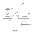
In the example of FIG. 2 , the ablation system 100 of FIG. 1 is employed to ablate the silicon nitride film 211, the amorphous silicon film 212, and the oxide film 213 to form a hole through them and expose the diffusion regions 203 and 204. The ablation process is illustrated in FIG. 3 , where the ablation step formed holes 220 exposing the diffusion regions 203 and 204. This allows for formation of metal contacts 221 to be formed in the holes 220, as illustrated in FIG. 4 . The metal contacts 221 allow external electrical circuits to make electrical connection to the diffusion regions 203 and 204.
In one embodiment, the amorphous silicon film 212 is absorptive in the wavelength of the laser generated by the laser source 102. That is, the amorphous silicon film 212 absorbs the energy of the laser pulses 103 at the wavelength of operation of the laser source 102, making it relatively difficult to achieve complete ablation of the oxide film 213 using a single laser pulse within one repetition. In one embodiment, the laser source 102 is a 532 nm laser in that it generates laser beam at a wavelength of 532 nm.
In one embodiment, the laser source 102 is configured to fire a burst of laser pulses in a single pulse repetition to form the holes 220 in a single ablation step. FIG. 5 schematically illustrates a burst of laser pulses fired by the laser source 102 in accordance with an embodiment of the present invention. In the example of FIG. 5 , a burst of laser pulses 510 and 511 are fired by the laser source 102 one after the other. The laser source 102 is configured to fire the laser pulses 510 and 511 at a repetition rate. Each pulse repetition is labeled as 501 (i.e., 501-1, 501-2, etc.) in FIG. 5 . Note that while two repetitions are shown in FIGS. 5 and 6 , embodiments of the present invention allow for complete ablation of the film stack in one repetition. Within a single repetition 501, the laser pulse 511 is fired a time delay (labeled as 502) after the laser pulse 510. The delay time 502 may be between 1 ns and 1 μs, for example. In general, the delay time between the laser pulses 510 and 511 is selected such that the laser pulses 510 and 511 are not noticeably separated on the ablation point on the solar cell due to the relatively slower motion of the laser scanner 104. The amplitude of the laser pulse 511 is lower than that of the laser pulse 510. That is, the laser pulse 511 has less pulse energy (e.g., about 37% to 50% less energy) than the laser pulse 510. The laser pulse 510 ablates the silicon nitride film 211 and the amorphous silicon film 212 to form a hole through them. The laser pulse 511, after a delay time 502 in the same repetition, ablates the oxide film 213 to complete the hole through the film stack 210 and thereby exposes the polysilicon layer 202. The lesser energy of the laser pulse 511 minimizes damage to material under the oxide film 213. Depending on the application, the energy of the laser pulse 511 may also be equal or less than the energy of the laser pulse 510.
The pulse energies of the laser pulses 510 and 511 may be varied depending on the type and thicknesses of the films being ablated. In one embodiment, the pulse energy of the laser pulse 510 is 10 μJ in a case where the thickness of the silicon nitride film 211 is 300 angstroms, the thickness of the amorphous silicon film 212 is 40 angstroms, and the thickness of the oxide film 213 is 120 angstroms. The pulse energy of the laser pulse 511 is set to approximately 37% of that of the laser pulse 510 in that example.
Still referring to FIG. 5 , the laser pulse 510 has a pulse width 503 and the laser pulse 511 has a pulse width 504. The laser pulses 510 and 503 are “burst” in that they are fired relatively close to each other. A commercially available laser 103 with burst mode is available from Lumera Laser GmbH of Germany. In one embodiment, the pulse width 503 is 14 ps and the pulse width 504 is also 14 ps, with a delay 502 of 20 ns, at a pulse repetition rate of 200 kHz (spacing for 501-1).
In another embodiment, the laser source 102 is configured to fire a single temporally asymmetric laser pulse in a single pulse repetition to form the holes 220 in a single ablation step. This embodiment is schematically shown in FIG. 6 , where the laser source 102 firing at a pulse repetition rate fires a single temporally asymmetric laser pulse 610 within a single pulse repetition 601 (i.e., 601-1, 601-2, etc.). As its name implies, the laser pulse 610 is asymmetric in time, having a first peak 605 in the earlier part of the laser pulse 610 and a second peak 606 in the later part of the pulse. In general, as shown in FIG. 6 , the earlier time portion of the laser pulse 610 is configured to have higher intensity compared to the later time portion of the laser pulse 610. The relative intensities between the two portions of the laser pulse 610 is controlled such that residue after the earlier portion is removed during the later portion to achieve complete laser ablation without inducing laser damage. Because the laser energy is continuously maintained during the ablation, the residue left form the earlier portion is still in the elevated temperature and can be removed at lower fluence than in room temperature ablation. An example laser source 102 that may be configured to generate a single temporally asymmetric pulse per repetition is commercially available from SPI Lasers.
In one embodiment, the peak 605 ablates the silicon nitride film 211 and the amorphous silicon film 212 to form a hole through them, and the peak 606 ablates the oxide film 213 to complete the hole through the film stack 210 and thereby exposes the polysilicon layer 202. The lesser intensity of the peak 606 minimizes damage to material under the oxide film 213. In one embodiment, the laser pulse 610 has a wavelength of 532 nm.
The intensities of peaks 605 and 606 may be varied depending on the type and thicknesses of the films being ablated. In one embodiment, the intensity of the peak 605 is 10 μJ and the intensity of the peak 606 is 3 μJ in a case where the thickness of the silicon nitride film 211 is 300 angstroms, the thickness of the amorphous silicon film 212 is 40 angstroms, and the thickness of the oxide film 213 is 120 angstroms. The pulse 610 has a pulse width 604, with the peak 605 having a width 602 and the peak 606 having a width 603. In the just mentioned example, the pulse width 604 is 20 ns the pulse width 602 is 10 ps and the pulse width 603 is 20 ns at a pulse repetition rate of 200 kHz.
Techniques for ablating film stacks in solar cell fabrication processes have been disclosed. While specific embodiments of the present invention have been provided, it is to be understood that these embodiments are for illustration purposes and not limiting. Many additional embodiments will be apparent to persons of ordinary skill in the art reading this disclosure.
Claims (20)
1. A method of fabricating a solar cell, the method comprising:
providing a film stack comprising a first film and a second film, the first film being formed over the second film, the first film comprising silicon, the first film and the second film being over a silicon substrate; and
in a single pulse repetition of a laser source firing at a pulse repetition rate, forming a hole through the first film and the second film.
2. The method of claim 1 wherein the first film comprises silicon nitride.
3. The method of claim 1 wherein a first laser pulse and a second laser pulse are fired within the single pulse repetition, the second laser pulse being fired after a delay time after firing the first laser pulse.
4. The method of claim 3 wherein the first laser pulse has a higher energy than the second laser pulse.
5. The method of claim 3 wherein the first laser pulse forms the hole through the first film and the second film, and the second laser pulse forms the hole through a third film that is between the second film and the silicon substrate.
6. The method of claim 1 wherein the second film comprises an oxide.
7. The method of claim 1 wherein the hole exposes a diffusion region of the solar cell.
8. The method of claim 1 wherein a temporally asymmetric laser pulse having a first peak and a second peak is fired within the single pulse repetition, the first peak having an energy higher than that of the second peak.
9. A method of fabricating a solar cell, the method comprising:
firing one laser pulse within a single repetition of a laser source that is firing laser pulses at a repetition rate, the one laser pulse being temporally asymmetric and having a first peak and a second peak, the first peak occurring first in time relative to the second peak in the single repetition, the first peak having an energy higher than that of the second peak; and
ablating a first film and a second film of a film stack with the one laser pulse within the single repetition, the first film comprising silicon, the film stack being over a silicon substrate.
10. The method of claim 9 wherein the first film comprises silicon nitride.
11. The method of claim 9 further comprising:
ablating a third film of the film stack with the one laser pulse within the single repetition.
12. The method of claim 11 wherein the first peak ablates the first film and the second film.
13. The method of claim 9 wherein the second film comprises an oxide.
14. The method of claim 9 wherein the hole exposes a diffusion region of the solar cell.
15. A method of fabricating a solar cell, the method comprising:
firing laser pulses from a laser source that fires at a pulse repetition rate; and
forming a hole through a first film and a second film of a film stack in a single pulse repetition of the laser source, the first film comprising silicon, the film stack being over a silicon substrate.
16. The method of claim 15 wherein the first film comprises silicon nitride.
17. The method of claim 15 wherein the second film comprises an oxide.
18. The method of claim 15 wherein a first laser pulse and a second laser pulse are fired by the laser source in the single pulse repetition.
19. The method of claim 18 wherein the first laser pulse forms the hole through the first film and the second film.
20. The method of claim 15 wherein the hole exposes a diffusion region of the solar cell.
Priority Applications (1)
| Application Number | Priority Date | Filing Date | Title |
|---|---|---|---|
| US13/486,095 US8409902B1 (en) | 2010-06-07 | 2012-06-01 | Ablation of film stacks in solar cell fabrication processes |
Applications Claiming Priority (2)
| Application Number | Priority Date | Filing Date | Title |
|---|---|---|---|
| US12/795,526 US8211731B2 (en) | 2010-06-07 | 2010-06-07 | Ablation of film stacks in solar cell fabrication processes |
| US13/486,095 US8409902B1 (en) | 2010-06-07 | 2012-06-01 | Ablation of film stacks in solar cell fabrication processes |
Related Parent Applications (1)
| Application Number | Title | Priority Date | Filing Date |
|---|---|---|---|
| US12/795,526 Continuation US8211731B2 (en) | 2010-06-07 | 2010-06-07 | Ablation of film stacks in solar cell fabrication processes |
Publications (1)
| Publication Number | Publication Date |
|---|---|
| US8409902B1 true US8409902B1 (en) | 2013-04-02 |
Family
ID=45064778
Family Applications (2)
| Application Number | Title | Priority Date | Filing Date |
|---|---|---|---|
| US12/795,526 Active US8211731B2 (en) | 2010-06-07 | 2010-06-07 | Ablation of film stacks in solar cell fabrication processes |
| US13/486,095 Active US8409902B1 (en) | 2010-06-07 | 2012-06-01 | Ablation of film stacks in solar cell fabrication processes |
Family Applications Before (1)
| Application Number | Title | Priority Date | Filing Date |
|---|---|---|---|
| US12/795,526 Active US8211731B2 (en) | 2010-06-07 | 2010-06-07 | Ablation of film stacks in solar cell fabrication processes |
Country Status (6)
| Country | Link |
|---|---|
| US (2) | US8211731B2 (en) |
| EP (1) | EP2576128A4 (en) |
| JP (3) | JP5647340B2 (en) |
| KR (1) | KR101877071B1 (en) |
| CN (1) | CN102939183B (en) |
| WO (1) | WO2011156043A1 (en) |
Cited By (12)
| Publication number | Priority date | Publication date | Assignee | Title |
|---|---|---|---|---|
| US20120276685A1 (en) * | 2008-12-04 | 2012-11-01 | Smith David D | Backside contact solar cell with formed polysilicon doped regions |
| USD822890S1 (en) | 2016-09-07 | 2018-07-10 | Felxtronics Ap, Llc | Lighting apparatus |
| USD832494S1 (en) | 2017-08-09 | 2018-10-30 | Flex Ltd. | Lighting module heatsink |
| USD832495S1 (en) | 2017-08-18 | 2018-10-30 | Flex Ltd. | Lighting module locking mechanism |
| USD833061S1 (en) | 2017-08-09 | 2018-11-06 | Flex Ltd. | Lighting module locking endcap |
| USD846793S1 (en) | 2017-08-09 | 2019-04-23 | Flex Ltd. | Lighting module locking mechanism |
| USD862777S1 (en) | 2017-08-09 | 2019-10-08 | Flex Ltd. | Lighting module wide distribution lens |
| USD862778S1 (en) | 2017-08-22 | 2019-10-08 | Flex Ltd | Lighting module lens |
| USD872319S1 (en) | 2017-08-09 | 2020-01-07 | Flex Ltd. | Lighting module LED light board |
| USD877964S1 (en) | 2017-08-09 | 2020-03-10 | Flex Ltd. | Lighting module |
| USD888323S1 (en) | 2017-09-07 | 2020-06-23 | Flex Ltd | Lighting module wire guard |
| US10775030B2 (en) | 2017-05-05 | 2020-09-15 | Flex Ltd. | Light fixture device including rotatable light modules |
Families Citing this family (17)
| Publication number | Priority date | Publication date | Assignee | Title |
|---|---|---|---|---|
| US9508886B2 (en) | 2007-10-06 | 2016-11-29 | Solexel, Inc. | Method for making a crystalline silicon solar cell substrate utilizing flat top laser beam |
| US9455362B2 (en) | 2007-10-06 | 2016-09-27 | Solexel, Inc. | Laser irradiation aluminum doping for monocrystalline silicon substrates |
| JP5473414B2 (en) * | 2009-06-10 | 2014-04-16 | 株式会社ディスコ | Laser processing equipment |
| US20120318776A1 (en) * | 2009-09-24 | 2012-12-20 | Electro Scientific Industries, Inc. | Method and apparatus for machining a workpiece |
| US8211731B2 (en) | 2010-06-07 | 2012-07-03 | Sunpower Corporation | Ablation of film stacks in solar cell fabrication processes |
| US8263899B2 (en) | 2010-07-01 | 2012-09-11 | Sunpower Corporation | High throughput solar cell ablation system |
| US8586403B2 (en) * | 2011-02-15 | 2013-11-19 | Sunpower Corporation | Process and structures for fabrication of solar cells with laser ablation steps to form contact holes |
| US8692111B2 (en) * | 2011-08-23 | 2014-04-08 | Sunpower Corporation | High throughput laser ablation processes and structures for forming contact holes in solar cells |
| JP6383291B2 (en) * | 2011-12-26 | 2018-08-29 | ソレクセル、インコーポレイテッド | System and method for improving light capture of solar cells |
| US8513045B1 (en) | 2012-01-31 | 2013-08-20 | Sunpower Corporation | Laser system with multiple laser pulses for fabrication of solar cells |
| JP6334675B2 (en) * | 2013-03-15 | 2018-05-30 | サンパワー コーポレイション | Solar cell and manufacturing method thereof |
| EP3206233A1 (en) * | 2016-02-12 | 2017-08-16 | Lg Electronics Inc. | Solar cell and method of manufacturing the same |
| CN106271089B (en) * | 2016-09-30 | 2019-01-25 | 英诺激光科技股份有限公司 | A kind of laser film etching device and method |
| GB2572608A (en) * | 2018-04-03 | 2019-10-09 | Ilika Tech Ltd | Laser processing method for thin film structures |
| GB2575786B (en) * | 2018-07-20 | 2021-11-03 | Dyson Technology Ltd | Stack for an energy storage device |
| US10615044B1 (en) * | 2018-10-18 | 2020-04-07 | Asm Technology Singapore Pte Ltd | Material cutting using laser pulses |
| KR102214451B1 (en) * | 2019-03-15 | 2021-02-09 | 한국과학기술연구원 | Method of forming local back surface field of solar cell using pulsed laser and solar cell including local back surface field formed thereby |
Citations (20)
| Publication number | Priority date | Publication date | Assignee | Title |
|---|---|---|---|---|
| US4322571A (en) | 1980-07-17 | 1982-03-30 | The Boeing Company | Solar cells and methods for manufacture thereof |
| US5432015A (en) | 1992-05-08 | 1995-07-11 | Westaim Technologies, Inc. | Electroluminescent laminate with thick film dielectric |
| US5738731A (en) | 1993-11-19 | 1998-04-14 | Mega Chips Corporation | Photovoltaic device |
| US5821590A (en) | 1995-07-24 | 1998-10-13 | Samsung Electronics Co., Ltd. | Semiconductor interconnection device with both n- and p-doped regions |
| US20060060238A1 (en) | 2004-02-05 | 2006-03-23 | Advent Solar, Inc. | Process and fabrication methods for emitter wrap through back contact solar cells |
| US20060196535A1 (en) | 2005-03-03 | 2006-09-07 | Swanson Richard M | Preventing harmful polarization of solar cells |
| US7175706B2 (en) * | 2002-02-28 | 2007-02-13 | Canon Kabushiki Kaisha | Process of producing multicrystalline silicon substrate and solar cell |
| US20080035198A1 (en) | 2004-10-14 | 2008-02-14 | Institut Fur Solarenergieforschung Gmbh | Method for the Contact Separation of Electrically-Conducting Layers on the Back Contacts of Solar Cells and Corresponding Solar Cells |
| US20080157283A1 (en) | 2006-10-09 | 2008-07-03 | Mehrdad Moslehi | Template for three-dimensional thin-film solar cell manufacturing and methods of use |
| US20080299297A1 (en) | 2007-05-29 | 2008-12-04 | Peter John Cousins | Array of small contacts for solar cell fabrication |
| US20090107545A1 (en) | 2006-10-09 | 2009-04-30 | Soltaix, Inc. | Template for pyramidal three-dimensional thin-film solar cell manufacturing and methods of use |
| US20090151784A1 (en) | 2007-12-14 | 2009-06-18 | Hsin-Chiao Luan | Anti-Reflective Coating With High Optical Absorption Layer For Backside Contact Solar Cells |
| US20090188553A1 (en) | 2008-01-25 | 2009-07-30 | Emat Technology, Llc | Methods of fabricating solar-cell structures and resulting solar-cell structures |
| US20090239331A1 (en) | 2008-03-24 | 2009-09-24 | Palo Alto Research Center Incorporated | Methods for forming multiple-layer electrode structures for silicon photovoltaic cells |
| US20090308457A1 (en) | 2008-06-12 | 2009-12-17 | Smith David D | Trench Process And Structure For Backside Contact Solar Cells With Polysilicon Doped Regions |
| US20100062560A1 (en) | 2008-09-10 | 2010-03-11 | Stion Corporation | Application specific solar cell and method for manufacture using thin film photovoltaic materials |
| US20100276405A1 (en) | 2008-03-31 | 2010-11-04 | Electro Scientific Industries, Inc. | Laser systems and methods using triangular-shaped tailored laser pulses for selected target classes |
| US20100304522A1 (en) | 2009-05-05 | 2010-12-02 | Solexel, Inc. | Ion implantation fabrication process for thin-film crystalline silicon solar cells |
| US20120028399A1 (en) | 2007-10-06 | 2012-02-02 | Solexel, Inc. | Laser processing for high-efficiency thin crystalline silicon solar cell fabrication |
| US8211731B2 (en) | 2010-06-07 | 2012-07-03 | Sunpower Corporation | Ablation of film stacks in solar cell fabrication processes |
Family Cites Families (18)
| Publication number | Priority date | Publication date | Assignee | Title |
|---|---|---|---|---|
| US5841099A (en) * | 1994-07-18 | 1998-11-24 | Electro Scientific Industries, Inc. | Method employing UV laser pulses of varied energy density to form depthwise self-limiting blind vias in multilayered targets |
| JP2000301369A (en) * | 1999-04-16 | 2000-10-31 | Hitachi Ltd | Laser texturing method, device therefor and substrate for magnetic disk |
| US7838794B2 (en) | 1999-12-28 | 2010-11-23 | Gsi Group Corporation | Laser-based method and system for removing one or more target link structures |
| WO2001074529A2 (en) * | 2000-03-30 | 2001-10-11 | Electro Scientific Industries, Inc. | Laser system and method for single pass micromachining of multilayer workpieces |
| DE10125397B4 (en) * | 2001-05-23 | 2005-03-03 | Siemens Ag | Method for drilling microholes with a laser beam |
| ATE311736T1 (en) * | 2001-09-01 | 2005-12-15 | Trumpf Lasertechnik Gmbh | METHOD FOR MAKING HOLES IN A MULTI-LAYER CIRCUIT BOARD |
| US7388147B2 (en) * | 2003-04-10 | 2008-06-17 | Sunpower Corporation | Metal contact structure for solar cell and method of manufacture |
| WO2005018064A2 (en) * | 2003-08-19 | 2005-02-24 | Electro Scientific Industries, Inc | Generating sets of tailored laser pulses |
| US7173212B1 (en) * | 2004-02-13 | 2007-02-06 | Semak Vladimir V | Method and apparatus for laser cutting and drilling of semiconductor materials and glass |
| US7491909B2 (en) * | 2004-03-31 | 2009-02-17 | Imra America, Inc. | Pulsed laser processing with controlled thermal and physical alterations |
| US7396706B2 (en) * | 2004-12-09 | 2008-07-08 | Electro Scientific Industries, Inc. | Synchronization technique for forming a substantially stable laser output pulse profile having different wavelength peaks |
| EP1763086A1 (en) * | 2005-09-09 | 2007-03-14 | Interuniversitair Micro-Elektronica Centrum | Photovoltaic cell with thick silicon oxide and silicon nitride passivation and fabrication method |
| US20070169806A1 (en) | 2006-01-20 | 2007-07-26 | Palo Alto Research Center Incorporated | Solar cell production using non-contact patterning and direct-write metallization |
| US20080029152A1 (en) * | 2006-08-04 | 2008-02-07 | Erel Milshtein | Laser scribing apparatus, systems, and methods |
| EP2239788A4 (en) * | 2008-01-30 | 2017-07-12 | Kyocera Corporation | Solar battery element and solar battery element manufacturing method |
| JP4964186B2 (en) * | 2008-04-28 | 2012-06-27 | 三菱電機株式会社 | Method for manufacturing photovoltaic device |
| JP2012501249A (en) * | 2008-08-26 | 2012-01-19 | アプライド マテリアルズ インコーポレイテッド | Laser material removal method and apparatus |
| US20100071765A1 (en) * | 2008-09-19 | 2010-03-25 | Peter Cousins | Method for fabricating a solar cell using a direct-pattern pin-hole-free masking layer |
-
2010
- 2010-06-07 US US12/795,526 patent/US8211731B2/en active Active
-
2011
- 2011-03-24 CN CN201180028121.1A patent/CN102939183B/en active Active
- 2011-03-24 KR KR1020127034342A patent/KR101877071B1/en active IP Right Grant
- 2011-03-24 JP JP2013514168A patent/JP5647340B2/en active Active
- 2011-03-24 WO PCT/US2011/029741 patent/WO2011156043A1/en active Application Filing
- 2011-03-24 EP EP11792819.2A patent/EP2576128A4/en active Pending
-
2012
- 2012-06-01 US US13/486,095 patent/US8409902B1/en active Active
-
2014
- 2014-11-06 JP JP2014226071A patent/JP5902791B2/en active Active
-
2016
- 2016-03-10 JP JP2016047147A patent/JP6352964B2/en active Active
Patent Citations (21)
| Publication number | Priority date | Publication date | Assignee | Title |
|---|---|---|---|---|
| US4322571A (en) | 1980-07-17 | 1982-03-30 | The Boeing Company | Solar cells and methods for manufacture thereof |
| US5432015A (en) | 1992-05-08 | 1995-07-11 | Westaim Technologies, Inc. | Electroluminescent laminate with thick film dielectric |
| US5738731A (en) | 1993-11-19 | 1998-04-14 | Mega Chips Corporation | Photovoltaic device |
| US5821590A (en) | 1995-07-24 | 1998-10-13 | Samsung Electronics Co., Ltd. | Semiconductor interconnection device with both n- and p-doped regions |
| US7175706B2 (en) * | 2002-02-28 | 2007-02-13 | Canon Kabushiki Kaisha | Process of producing multicrystalline silicon substrate and solar cell |
| US20060060238A1 (en) | 2004-02-05 | 2006-03-23 | Advent Solar, Inc. | Process and fabrication methods for emitter wrap through back contact solar cells |
| US20080035198A1 (en) | 2004-10-14 | 2008-02-14 | Institut Fur Solarenergieforschung Gmbh | Method for the Contact Separation of Electrically-Conducting Layers on the Back Contacts of Solar Cells and Corresponding Solar Cells |
| US20060196535A1 (en) | 2005-03-03 | 2006-09-07 | Swanson Richard M | Preventing harmful polarization of solar cells |
| US20090107545A1 (en) | 2006-10-09 | 2009-04-30 | Soltaix, Inc. | Template for pyramidal three-dimensional thin-film solar cell manufacturing and methods of use |
| US20080157283A1 (en) | 2006-10-09 | 2008-07-03 | Mehrdad Moslehi | Template for three-dimensional thin-film solar cell manufacturing and methods of use |
| US8129822B2 (en) | 2006-10-09 | 2012-03-06 | Solexel, Inc. | Template for three-dimensional thin-film solar cell manufacturing and methods of use |
| US20080299297A1 (en) | 2007-05-29 | 2008-12-04 | Peter John Cousins | Array of small contacts for solar cell fabrication |
| US20120028399A1 (en) | 2007-10-06 | 2012-02-02 | Solexel, Inc. | Laser processing for high-efficiency thin crystalline silicon solar cell fabrication |
| US20090151784A1 (en) | 2007-12-14 | 2009-06-18 | Hsin-Chiao Luan | Anti-Reflective Coating With High Optical Absorption Layer For Backside Contact Solar Cells |
| US20090188553A1 (en) | 2008-01-25 | 2009-07-30 | Emat Technology, Llc | Methods of fabricating solar-cell structures and resulting solar-cell structures |
| US20090239331A1 (en) | 2008-03-24 | 2009-09-24 | Palo Alto Research Center Incorporated | Methods for forming multiple-layer electrode structures for silicon photovoltaic cells |
| US20100276405A1 (en) | 2008-03-31 | 2010-11-04 | Electro Scientific Industries, Inc. | Laser systems and methods using triangular-shaped tailored laser pulses for selected target classes |
| US20090308457A1 (en) | 2008-06-12 | 2009-12-17 | Smith David D | Trench Process And Structure For Backside Contact Solar Cells With Polysilicon Doped Regions |
| US20100062560A1 (en) | 2008-09-10 | 2010-03-11 | Stion Corporation | Application specific solar cell and method for manufacture using thin film photovoltaic materials |
| US20100304522A1 (en) | 2009-05-05 | 2010-12-02 | Solexel, Inc. | Ion implantation fabrication process for thin-film crystalline silicon solar cells |
| US8211731B2 (en) | 2010-06-07 | 2012-07-03 | Sunpower Corporation | Ablation of film stacks in solar cell fabrication processes |
Non-Patent Citations (2)
| Title |
|---|
| Overview: Lumera Laser Products, Jan. 2009, pp. 1-12. |
| Unitek Miyachi Lasers Connections, "Understanding Laser Parameters for Weld Development" Technical Application Brief, 2003, 2 sheets, vol. 1/No. 3. |
Cited By (20)
| Publication number | Priority date | Publication date | Assignee | Title |
|---|---|---|---|---|
| US20120276685A1 (en) * | 2008-12-04 | 2012-11-01 | Smith David D | Backside contact solar cell with formed polysilicon doped regions |
| US8647911B2 (en) * | 2008-12-04 | 2014-02-11 | Sunpower Corporation | Backside contact solar cell with formed polysilicon doped regions |
| USD822890S1 (en) | 2016-09-07 | 2018-07-10 | Felxtronics Ap, Llc | Lighting apparatus |
| US10775030B2 (en) | 2017-05-05 | 2020-09-15 | Flex Ltd. | Light fixture device including rotatable light modules |
| USD853629S1 (en) | 2017-08-09 | 2019-07-09 | Flex Ltd | Lighting module locking mechanism |
| USD877964S1 (en) | 2017-08-09 | 2020-03-10 | Flex Ltd. | Lighting module |
| USD846793S1 (en) | 2017-08-09 | 2019-04-23 | Flex Ltd. | Lighting module locking mechanism |
| USD853625S1 (en) | 2017-08-09 | 2019-07-09 | Flex Ltd | Lighting module heatsink |
| USD1010915S1 (en) | 2017-08-09 | 2024-01-09 | Linmore Labs Led, Inc. | Lighting module |
| USD853627S1 (en) | 2017-08-09 | 2019-07-09 | Flex Ltd | Lighting module locking endcap |
| USD905325S1 (en) | 2017-08-09 | 2020-12-15 | Flex Ltd | Lighting module |
| USD862777S1 (en) | 2017-08-09 | 2019-10-08 | Flex Ltd. | Lighting module wide distribution lens |
| USD832494S1 (en) | 2017-08-09 | 2018-10-30 | Flex Ltd. | Lighting module heatsink |
| USD872319S1 (en) | 2017-08-09 | 2020-01-07 | Flex Ltd. | Lighting module LED light board |
| USD833061S1 (en) | 2017-08-09 | 2018-11-06 | Flex Ltd. | Lighting module locking endcap |
| USD885615S1 (en) | 2017-08-09 | 2020-05-26 | Flex Ltd. | Lighting module LED light board |
| USD832495S1 (en) | 2017-08-18 | 2018-10-30 | Flex Ltd. | Lighting module locking mechanism |
| USD853628S1 (en) | 2017-08-18 | 2019-07-09 | Flex Ltd. | Lighting module locking mechanism |
| USD862778S1 (en) | 2017-08-22 | 2019-10-08 | Flex Ltd | Lighting module lens |
| USD888323S1 (en) | 2017-09-07 | 2020-06-23 | Flex Ltd | Lighting module wire guard |
Also Published As
| Publication number | Publication date |
|---|---|
| JP6352964B2 (en) | 2018-07-04 |
| EP2576128A1 (en) | 2013-04-10 |
| CN102939183B (en) | 2015-11-25 |
| KR20130086302A (en) | 2013-08-01 |
| EP2576128A4 (en) | 2018-01-17 |
| JP5902791B2 (en) | 2016-04-13 |
| US20110300665A1 (en) | 2011-12-08 |
| JP5647340B2 (en) | 2014-12-24 |
| JP2013528326A (en) | 2013-07-08 |
| JP2016129256A (en) | 2016-07-14 |
| US8211731B2 (en) | 2012-07-03 |
| JP2015062242A (en) | 2015-04-02 |
| WO2011156043A1 (en) | 2011-12-15 |
| KR101877071B1 (en) | 2018-07-10 |
| CN102939183A (en) | 2013-02-20 |
Similar Documents
| Publication | Publication Date | Title |
|---|---|---|
| US8409902B1 (en) | Ablation of film stacks in solar cell fabrication processes | |
| US11437528B2 (en) | Process and structures for fabrication of solar cells | |
| JP6111249B2 (en) | High throughput laser ablation process and structure for forming contact holes in solar cells | |
| US10199521B2 (en) | Thick damage buffer for foil-based metallization of solar cells |
Legal Events
| Date | Code | Title | Description |
|---|---|---|---|
| STCF | Information on status: patent grant |
Free format text: PATENTED CASE |
|
| FPAY | Fee payment |
Year of fee payment: 4 |
|
| MAFP | Maintenance fee payment |
Free format text: PAYMENT OF MAINTENANCE FEE, 8TH YEAR, LARGE ENTITY (ORIGINAL EVENT CODE: M1552); ENTITY STATUS OF PATENT OWNER: LARGE ENTITY Year of fee payment: 8 |
|
| AS | Assignment |
Owner name: MAXEON SOLAR PTE. LTD., SINGAPORE Free format text: ASSIGNMENT OF ASSIGNORS INTEREST;ASSIGNOR:SUNPOWER CORPORATION;REEL/FRAME:062490/0742 Effective date: 20221214 |