US8118585B2 - Pattern formation method and a method for manufacturing a semiconductor device - Google Patents
Pattern formation method and a method for manufacturing a semiconductor device Download PDFInfo
- Publication number
- US8118585B2 US8118585B2 US12/882,944 US88294410A US8118585B2 US 8118585 B2 US8118585 B2 US 8118585B2 US 88294410 A US88294410 A US 88294410A US 8118585 B2 US8118585 B2 US 8118585B2
- Authority
- US
- United States
- Prior art keywords
- template
- pattern
- projection
- workpiece substrate
- pattern formation
- Prior art date
- Legal status (The legal status is an assumption and is not a legal conclusion. Google has not performed a legal analysis and makes no representation as to the accuracy of the status listed.)
- Active
Links
Images


Classifications
-
- G—PHYSICS
- G03—PHOTOGRAPHY; CINEMATOGRAPHY; ANALOGOUS TECHNIQUES USING WAVES OTHER THAN OPTICAL WAVES; ELECTROGRAPHY; HOLOGRAPHY
- G03F—PHOTOMECHANICAL PRODUCTION OF TEXTURED OR PATTERNED SURFACES, e.g. FOR PRINTING, FOR PROCESSING OF SEMICONDUCTOR DEVICES; MATERIALS THEREFOR; ORIGINALS THEREFOR; APPARATUS SPECIALLY ADAPTED THEREFOR
- G03F7/00—Photomechanical, e.g. photolithographic, production of textured or patterned surfaces, e.g. printing surfaces; Materials therefor, e.g. comprising photoresists; Apparatus specially adapted therefor
- G03F7/0002—Lithographic processes using patterning methods other than those involving the exposure to radiation, e.g. by stamping
-
- B—PERFORMING OPERATIONS; TRANSPORTING
- B82—NANOTECHNOLOGY
- B82Y—SPECIFIC USES OR APPLICATIONS OF NANOSTRUCTURES; MEASUREMENT OR ANALYSIS OF NANOSTRUCTURES; MANUFACTURE OR TREATMENT OF NANOSTRUCTURES
- B82Y10/00—Nanotechnology for information processing, storage or transmission, e.g. quantum computing or single electron logic
-
- B—PERFORMING OPERATIONS; TRANSPORTING
- B82—NANOTECHNOLOGY
- B82Y—SPECIFIC USES OR APPLICATIONS OF NANOSTRUCTURES; MEASUREMENT OR ANALYSIS OF NANOSTRUCTURES; MANUFACTURE OR TREATMENT OF NANOSTRUCTURES
- B82Y40/00—Manufacture or treatment of nanostructures
-
- G—PHYSICS
- G03—PHOTOGRAPHY; CINEMATOGRAPHY; ANALOGOUS TECHNIQUES USING WAVES OTHER THAN OPTICAL WAVES; ELECTROGRAPHY; HOLOGRAPHY
- G03F—PHOTOMECHANICAL PRODUCTION OF TEXTURED OR PATTERNED SURFACES, e.g. FOR PRINTING, FOR PROCESSING OF SEMICONDUCTOR DEVICES; MATERIALS THEREFOR; ORIGINALS THEREFOR; APPARATUS SPECIALLY ADAPTED THEREFOR
- G03F9/00—Registration or positioning of originals, masks, frames, photographic sheets or textured or patterned surfaces, e.g. automatically
Definitions
- Embodiments described herein relate generally to a pattern formation method and a method for manufacturing a semiconductor device.
- a fine circuit pattern is formed on the surface of a semiconductor wafer.
- a circuit pattern has been formed by a photolithography process. More specifically, a resist film is formed on the wafer. This resist film is exposed to light through a photomask, and then developed. Thus, the pattern formed on the photomask is transferred to the resist film to form a resist pattern. This resist pattern is used as a mask to process the wafer, thereby forming a circuit pattern.
- the cost related to the exposure apparatus used in such a photolithography process significantly increases with the miniaturization of the circuit pattern.
- One reason for this is that the cost of the exposure apparatus itself exponentially increases.
- various contrivances are needed in the photomask to obtain resolution comparable to the wavelength of light used.
- the cost of the photomask is also rapidly increasing.
- the nanoimprint lithography As a pattern formation technique to solve this problem, the nanoimprint lithography has been proposed.
- a pattern to be formed on a wafer is formed beforehand on a template.
- the template is pressed against a liquid resin material dropped on the wafer. With the template pressed, the resin material is cured.
- the pattern made of the resin material is formed (see, e.g., JP-A 2008-194980 (Kokai)). That is, the nanoimprint lithography is a one-to-one transfer technique.
- the pattern on the template is typically formed by performing EB writing and etching on a template substrate.
- the aforementioned nanoimprint lithography is broadly divided into a thermal nanoimprint lithography and an UV-nanoimprint lithography.
- a resin material is melted by heating.
- a template is pressed against the melted resin material.
- the resin material is cured by cooling.
- a transparent template made of e.g. glass is pressed against a liquid photocurable resin material. Then, this resin material is cured by ultraviolet irradiation.
- residual layer thickness The thickness of the layer of this remaining resin material (residual layer) is referred to as residual layer thickness (RLT).
- the residual layer thickness depends on various conditions, such as the amount of unevenness of the pattern formed on the template, the amount and location of the resist material dropped on the wafer, and the spread state of the resin material pressed by the template. In other words, the residual layer thickness is determined by circumstances.
- variation in the residual layer thickness involves variation in the condition for subsequent processing on the wafer. This makes it difficult to perform accurate processing on the wafer.
- FIG. 1 is a bottom view illustrating a template used in a first embodiment
- FIG. 2 is a cross-sectional view taken along line A-A′ shown in FIG. 1 ;
- FIGS. 3A to 3D are process cross-sectional views illustrating a method for fabricating a template of the first embodiment
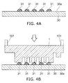
- FIGS. 4A and 4B are process cross-sectional views illustrating a pattern formation method according to the first embodiment
- FIG. 5 is a process cross-sectional view illustrating the pattern formation method according to the first embodiment
- FIGS. 6A to 6C are process cross-sectional views illustrating the pattern formation method according to the first embodiment
- FIG. 7 is a cross-sectional view illustrating a template used in a second embodiment
- FIG. 8 is a bottom view illustrating a template used in a third embodiment
- FIG. 9 is a bottom view illustrating a template used in a fourth embodiment.
- FIGS. 10A and 10B are process cross-sectional views illustrating a pattern formation method according to a fifth embodiment.
- FIGS. 11A and 11B are process cross-sectional views illustrating a pattern formation method according to a sixth embodiment.
- a pattern formation method can place a liquid resin material on a workpiece substrate.
- the method can press a template against the resin material and measuring distance between a lower surface of a projection of the template and an upper surface of the workpiece substrate.
- the template includes a pattern formation region and a circumferential region around the pattern formation region.
- a pattern for circuit pattern formation is formed in the pattern formation region and the projection is formed in the circumferential region.
- the method can form a resin pattern by curing the resin material in a state of pressing the template.
- the method can separate the template from the resin pattern.
- FIG. 1 is a bottom view illustrating the template used in this embodiment.
- FIG. 2 is a cross-sectional view taken along line A-A′ shown in FIG. 1 .
- a template 1 used in this embodiment is made of e.g. quartz.
- the template 1 is shaped like a rectangular plate.
- the central portion of the template 1 constitutes a pattern formation region Rp, which is surrounded by a circumferential region Rc.
- the pattern formation region Rp is shaped like a rectangle.
- the circumferential region Rc is shaped like a frame.
- the circumferential region Rc is recessed relative to the pattern formation region Rp. That is, in the lower surface of the template 1 , the region Sc located in the circumferential region Rc is placed above the region Sp located in the pattern formation region Rp.
- a pattern 11 for forming a circuit pattern of a semiconductor device is formed in the pattern formation region Rp.
- the lower surface of the template 1 is recessed to form trenches 12 .
- the portion between the trenches 12 constitutes a protrusion 13 .
- the pattern 11 is not shown.
- a projection 15 is formed at one position on the lower surface of the template 1 .
- the projection 15 is shaped like a rectangular solid, for instance.
- the lower surface 15 a of the projection 15 is flat.
- the lower surface 15 a of the projection 15 is located at the same height as the bottom surface 12 a of the trench 12 .
- the lower surface 15 a is located above the lower surface 13 a of the protrusion 13 .
- the width of the protrusion 13 is approximately 30 nm.
- the height of the protrusion 13 i.e., the depth of the trench 12 , is approximately 70 to 80 nm.
- FIGS. 3A to 3D are process cross-sectional views illustrating a method for fabricating a template of this embodiment.
- a substrate 20 made of quartz is prepared.
- the substrate 20 is shaped like a rectangular plate.
- a pattern formation region Rp and a circumferential region Rc are defined.
- an electron beam sensitive resist film is formed on the lower surface of the substrate 20 .
- This resist film is subjected to EB writing, and then developed to form a resist pattern 22 .
- the resist pattern 22 is used as a mask to perform dry etching.
- trenches 12 are formed in the pattern formation region Rp.
- a depression 21 is formed in a region intended for forming a projection 15 (see FIG. 2 ) in the circumferential region Rc.
- the remaining portion between the trenches 12 constitutes a protrusion 13 .
- a pattern 11 is formed.
- the depression 21 is formed by the same dry etching as the trench 12 , the depression 21 has the same depth as the trench 12 .
- the bottom surface 12 a of the trench 12 and the bottom surface 21 a of the depression 21 are flat. Subsequently, the resist pattern 22 is removed.
- a resist film 23 is formed so as to cover the overall pattern formation region Rp and the depression 21 in the circumferential region Rc.
- the resist film 23 is used as a mask to perform wet etching.
- the portion except the depression 21 in the circumferential region Rc is recessed.
- the recess depth at this time is made deeper than the depth of the trench 12 and the depression 21 .
- the region Sc located in the circumferential region Rc on the lower surface of the substrate 20 is located above the bottom surface 12 a of the trench 12 and the bottom surface 21 a of the depression 21 .
- the bottom surface 21 a protrudes downward relative to the region Sc. Consequently, a projection 15 is formed at the position where the depression 21 has been formed.
- the bottom surface 21 a of the depression 21 constitutes the lower surface 15 a of the projection 15 .
- the resist film 23 is removed.
- the vertical distance Xa between the lower surface 13 a of the protrusion 13 and the lower surface 15 a of the projection 15 is measured.
- the template 1 is fabricated.
- FIGS. 4A , 4 B, 5 , 6 A to 6 C are process cross-sectional views illustrating a pattern formation method according to this embodiment.
- the workpiece substrate 30 may be, for instance, a semiconductor wafer such as a silicon wafer, a semiconductor wafer with a conductive film such as a polysilicon film formed thereon, or a semiconductor wafer with an interlayer insulating film formed thereon.
- a liquid resin material 31 is dropped on the upper surface 30 a of the workpiece substrate 30 .
- the resin material 31 is a photocurable resin material which is cured by ultraviolet irradiation.
- droplets of the resin material 31 are placed at a plurality of positions on the workpiece substrate 30 .
- “liquid” refers to a state of fluidity enough to enable molding by the nanoimprint lithography, and includes the semi-liquid state.
- a moving unit 101 holds the template 1 , places the template 1 immediately above the workpiece substrate 30 , and lowers the template 1 until the template 1 is brought into contact with the droplets of the resin material 31 .
- the template 1 is pressed against the workpiece substrate 30 .
- the liquid resin material 31 is spread on the workpiece substrate 30 , and the trenches 12 are filled therewith.
- the resin material 31 remains as a residual layer 32 between the lower surface 13 a of the protrusion 13 and the upper surface 30 a of the workpiece substrate 30 .
- the layer thickness of this residual layer 32 i.e., the distance between the lower surface 13 a of the protrusion 13 and the upper surface 30 a of the workpiece substrate 30 , is the residual layer thickness RLT.
- the residual layer thickness RLT is determined by the spread state of the resin material 31 .
- the spread state of the resin material 31 depends on the dropped amount and placement of the resin material 31 . Hence, even if the template 1 is pressed with the same pressing force, the residual layer thickness RLT varies due to variation in the dropped amount and variation in the dropped position of the resin material 31 .
- the distance Xb between the lower surface 15 a of the projection 15 and the upper surface 30 a of the workpiece substrate 30 is measured.
- the template 1 is irradiated with laser light L from above.
- the laser light L is injected vertically downward into the template 1 from the upper surface of the template 1 immediately above the projection 15 .
- the laser light L is transmitted in the template 1 , and partly reflected at the lower surface 15 a of the projection 15 back to the laser interferometer 102 .
- the rest passes through the lower surface 15 a to the upper surface 30 a of the workpiece substrate 30 and is reflected at the upper surface 30 a .
- the laser interferometer 102 detects interference between the reflected light from the lower surface 15 a of the projection 15 and the reflected light from the upper surface 30 a of the workpiece substrate 30 to measure the distance Xb.
- the residual layer thickness RLT is calculated by the following equation (1).
- RLT Xb ⁇ Xa (1)
- the calculated value of the residual layer thickness RLT is fed back to the moving unit 101 for the template 1 .
- the moving unit 101 stops lowering the template 1 when the residual layer thickness RLT reaches the target value.
- the residual layer thickness RLT is made close to the target value.
- the target value of the residual layer thickness RLT is e.g. 10 nm.
- the template 1 is irradiated with ultraviolet radiation UV from above.
- the ultraviolet radiation UV is transmitted through the template 1 to the resin material 31 , and cures the resin material 31 .
- a resin pattern 33 made of the solid resin material 31 is formed on the workpiece substrate 30 .
- the resin pattern 33 is a transferred pattern of the pattern 11 of the template 1 .
- the moving unit 101 moves the template 1 upward and separates the template 1 from the resin pattern 33 .
- the resin pattern 33 is used as a mask to process the workpiece substrate 30 .
- the resin pattern 33 is used as a mask to etch the workpiece substrate 30 to process the semiconductor wafer, conductive film, or interlayer insulating film.
- the resin pattern 33 is used as a mask to implant impurity into the workpiece substrate 30 to form an impurity diffusion layer in the semiconductor wafer. Such processing is repeated to manufacture a semiconductor device.
- the template 1 is provided with a projection 15 .
- the vertical distance Xa between the lower surface 15 a of the projection 15 and the lower surface 13 a of the protrusion 13 is measured beforehand.
- the distance Xb between the lower surface 15 a of the projection 15 and the upper surface 30 a of the workpiece substrate 30 is measured.
- the residual layer thickness RLT can be calculated by the aforementioned equation (1).
- the calculated value of the residual layer thickness RLT is fed back to the moving unit 101 , so that the residual layer thickness RLT can be controlled. Consequently, variation in the residual layer thickness RLT can be suppressed.
- FIG. 6C variation in the condition for processing such as etching can be suppressed.
- accurate processing can be performed on the workpiece substrate 30 .
- a fine semiconductor device can be stably manufactured.
- the following may be considered as a different approach.
- the position of the upper surface (non-pressing surface) of the template is measured when the template is pressed against the resin material 31 .
- the distance between the upper surface of the template and the upper surface 30 a of the workpiece substrate 30 is determined.
- the residual layer thickness RLT is determined by subtracting the thickness of the template from this distance.
- the thickness of the template has a tolerance on the micron order.
- the residual layer thickness RLT is approximately 10 nm. Hence, it is extremely difficult to determine the residual layer thickness RLT based on the position of the upper surface of the template.
- the following may be considered as another different approach.
- the distance between the region Sc of the lower surface of the template located in the circumferential region Rc and the upper surface 30 a of the workpiece substrate 30 is measured by a laser interferometer, for instance.
- the residual layer thickness RLT is determined by subtracting the recessed amount of the circumferential region Rc from this distance.
- the recessing of the circumferential region Rc is performed by wet etching, the recessed amount has large variation.
- the region Sc is exposed to wet etching, the region Sc has large surface roughness. Thus, this approach is also impractical.
- the lower surface 15 a of the projection 15 is formed as the bottom surface 21 a of the depression 21 in the process shown in FIG. 3B .
- the depression 21 has the same depth as the trench 12 , such as approximately 70 to 80 nm. Hence, the depth of the depression 21 is considerably smaller than the overall thickness of the template 1 , and less prone to errors. Thus, variation in the distance Xa is small.
- the projection 15 protrudes downward, the distance Xb between the lower surface 15 a of the projection 15 and the upper surface 30 a of the workpiece substrate 30 is small. Hence, the measurement of the distance Xb is also less prone to errors.
- the depression 21 is formed by dry etching, the bottom surface 21 a of the depression 21 , i.e., the lower surface 15 a of the projection 15 , has high flatness. For these reasons, the distance Xb can be accurately measured. Consequently, the residual layer thickness RLT can be accurately determined.
- the lower surface 15 a of the projection 15 is located above the lower surface 13 a of the protrusion 13 .
- the projection 15 does not crush down the resin pattern 33 already formed in the adjacent chip region.
- the measurement value of the residual layer thickness RLT is fed back to the moving unit 101 for the template 1 .
- the invention is not limited thereto.
- the content and condition for the processing on the workpiece substrate 30 shown in FIG. 6C can be adjusted based on the measurement value of the residual layer thickness RLT of the resultant residual layer 32 .
- the etching time may be adjusted based on the residual layer thickness RLT, or the residual layer portion of the resin pattern 33 may be removed before etching.
- the acceleration voltage may be adjusted based on the residual layer thickness RLT.
- FIG. 7 is a cross-sectional view illustrating a template used in this embodiment.
- a template 2 in this embodiment is different from the template 1 (see FIG. 2 ) in that the projection 15 is replaced by a projection 25 .
- the projection 25 has a larger amount of protrusion than the projection 15 .
- the lower surface 25 a of the projection 25 is located below the bottom surface 12 a of the trench 12 , and above the lower surface 13 a of the protrusion 13 .
- Such a template 2 can be fabricated by forming the trenches 12 and the depression 21 by different etching processes in the process shown in FIG. 3B .
- the position of the lower surface 25 a of the projection 25 is lower, and the vertical distance Xa between the lower surface 25 a and the lower surface 13 a is smaller. Hence, the distance Xb can be measured more accurately. Consequently, the residual layer thickness RLT can be determined more accurately.
- the configuration and effect of this embodiment other than the foregoing are similar to those of the above first embodiment.
- FIG. 8 is a bottom view illustrating a template used in this embodiment.
- projections 35 a , 35 b , and 35 c are provided at three positions in the circumferential region Rc.
- the projections 35 a , 35 b , and 35 c are located at non-collinear positions.
- the lower surfaces of the projections 35 a , 35 b , and 35 c are located at an equal height, and are each flat. That is, the lower surfaces of the projections 35 a , 35 b , and 35 c constitute part of the same imaginary plane.
- the distance Xb is measured for each of the projections 35 a to 35 c .
- the direction and degree of the inclination of the template 3 with respect to the upper surface 30 a of the workpiece substrate 30 can be calculated.
- the pitch and roll of the template 3 can be detected to realize triaxial control.
- the projections may be formed at four or more positions in the circumferential region Rc.
- FIG. 9 is a bottom view illustrating a template used in this embodiment.
- a frame-shaped projection 45 is formed in the circumferential region Rc so as to surround the pattern formation region Rp.
- the lower surface 45 a of the projection 45 is flat, and parallel to the lower surface of the pattern formation region Rp.
- the distance Xb can be measured at an arbitrary position of the projection 45 , allowing multi-axial control.
- FIGS. 10A and 10B are process cross-sectional views illustrating a pattern formation method according to this embodiment.
- a through hole 51 penetrating through the template 5 is formed at the position corresponding to the projection 15 .
- the lower end of the through hole 51 opens at the lower surface 15 a of the projection 15 .
- the upper end of the through hole 51 opens at the upper surface of the template 5 immediately above the projection 15 .
- the distance Xb is measured using helium gas instead of the laser interferometer. More specifically, helium gas is passed into the through hole 51 to supply helium gas from above the template 5 into the space between the template 5 and the workpiece substrate 30 . Then, the flow resistance of helium gas is evaluated. For instance, with the supply pressure of helium gas kept constant, the flow amount of helium gas is measured.
- the distance Xb between the template 5 and the workpiece substrate 30 decreases, the resistance to the flow of helium gas increases, and the flow amount of helium gas decreases.
- the distance Xb can be estimated by measuring the flow amount of helium gas.
- the distance between the lower end of the through hole 51 and the workpiece substrate 30 is made shorter, and the flow resistance is made more sensitive to the distance Xb.
- helium gas is likely to remain in the trench 12 when the template 5 is pressed against the resin material 31 to fill the trench 12 with the resin material 31 .
- Helium gas has a small molecular size, and is easily diffused in the resin material 31 . Hence, as compared with the case where the resin material 31 is surrounded by the ambient atmosphere, air bubbles are less likely to remain in the trench 12 .
- the configuration and effect of this embodiment other than the foregoing are similar to those of the above first embodiment.
- other gases may be used to measure the distance Xb.
- FIGS. 11A and 11B are process cross-sectional views illustrating a pattern formation method according to this embodiment.
- this embodiment also uses the template 5 with the through hole 51 formed therein.
- the atmosphere gas is ejected upward.
- the atmosphere gas may be either ambient air or helium gas.
- the flow resistance of the gas flowing in the through hole 51 is evaluated. For instance, with the exhaust pressure kept constant, the flow amount of the gas flowing in the through hole 51 is measured. Also in this case, as in the above fifth embodiment, the distance Xb can be estimated based on the flow resistance of the gas. Furthermore, if the pressure around the resin material 31 is reduced to a vacuum, air bubbles are less likely to remain in the trench 12 .
- the configuration and effect of this embodiment other than the foregoing are similar to those of the above fifth embodiment.
- the resin material 31 is a photocurable resin material
- the template is formed from quartz.
- the resin material may be a thermosetting resin material.
- the template is formed from a metal, for instance.
- the distance Xb cannot be measured by a laser interferometer as in the above first embodiment.
- the distance Xb can be measured by evaluating the flow resistance of a gas.
- the methods based on a laser interferometer and the methods based on the flow resistance of a gas are used to measure the distance Xb.
- the invention is not limited thereto.
- the above embodiments can realize a pattern formation method capable of performing accurate processing on a workpiece substrate and a method for manufacturing a semiconductor device.
Abstract
Description
RLT=Xb−Xa (1)
Claims (18)
Applications Claiming Priority (2)
| Application Number | Priority Date | Filing Date | Title |
|---|---|---|---|
| JP2009-245411 | 2009-10-26 | ||
| JP2009245411A JP5419634B2 (en) | 2009-10-26 | 2009-10-26 | Pattern formation method |
Publications (2)
| Publication Number | Publication Date |
|---|---|
| US20110097827A1 US20110097827A1 (en) | 2011-04-28 |
| US8118585B2 true US8118585B2 (en) | 2012-02-21 |
Family
ID=43898779
Family Applications (1)
| Application Number | Title | Priority Date | Filing Date |
|---|---|---|---|
| US12/882,944 Active US8118585B2 (en) | 2009-10-26 | 2010-09-15 | Pattern formation method and a method for manufacturing a semiconductor device |
Country Status (2)
| Country | Link |
|---|---|
| US (1) | US8118585B2 (en) |
| JP (1) | JP5419634B2 (en) |
Families Citing this family (8)
| Publication number | Priority date | Publication date | Assignee | Title |
|---|---|---|---|---|
| JP5693488B2 (en) | 2012-02-20 | 2015-04-01 | 株式会社東芝 | Pattern forming method, pattern forming apparatus, and semiconductor device manufacturing method |
| JP6302287B2 (en) | 2014-03-04 | 2018-03-28 | 東芝メモリ株式会社 | Imprint apparatus and pattern forming method |
| FR3030875B1 (en) | 2014-12-22 | 2022-10-14 | Commissariat Energie Atomique | METHOD FOR OBTAINING PATTERNS IN A LAYER |
| US10578965B2 (en) * | 2016-03-31 | 2020-03-03 | Canon Kabushiki Kaisha | Pattern forming method |
| JP7149284B2 (en) * | 2017-03-16 | 2022-10-06 | モレキュラー インプリンツ, インコーポレイテッド | Optical polymer film and method of casting same |
| EP3697588B1 (en) | 2017-10-17 | 2024-04-03 | Magic Leap, Inc. | A system for molding a photocurable material into a planar object |
| JP7077754B2 (en) * | 2018-05-08 | 2022-05-31 | 大日本印刷株式会社 | Imprint mold substrate, imprint mold and their manufacturing method |
| EP3867677A4 (en) | 2018-10-16 | 2021-12-22 | Magic Leap, Inc. | Methods and apparatuses for casting polymer products |
Citations (11)
| Publication number | Priority date | Publication date | Assignee | Title |
|---|---|---|---|---|
| US20060192320A1 (en) * | 2005-02-28 | 2006-08-31 | Toshinobu Tokita | Pattern transferring mold, pattern transferring apparatus and device manufacturing method using the same |
| US20060266244A1 (en) * | 2005-05-31 | 2006-11-30 | Asml Netherlands B.V. | Imprint lithography |
| JP2007027361A (en) | 2005-07-15 | 2007-02-01 | Toppan Printing Co Ltd | Mold for imprint |
| US20070151328A1 (en) * | 2005-12-30 | 2007-07-05 | Asml Holding N.V. | Vacuum driven proximity sensor |
| US7247843B1 (en) * | 2006-05-11 | 2007-07-24 | Massachusetts Institute Of Technology | Long-range gap detection with interferometric sensitivity using spatial phase of interference patterns |
| JP2008078550A (en) | 2006-09-25 | 2008-04-03 | Toppan Printing Co Ltd | Imprint mold, its manufacturing method, and pattern formation method |
| US20080090170A1 (en) * | 2006-10-04 | 2008-04-17 | Ikuo Yoneda | Pattern forming template and pattern forming method |
| JP2008194980A (en) | 2007-02-14 | 2008-08-28 | Toshiba Mach Co Ltd | Transfer device and transfer method |
| US20090001634A1 (en) * | 2007-06-28 | 2009-01-01 | Elpida Memory, Inc. | Fine resist pattern forming method and nanoimprint mold structure |
| US20090023288A1 (en) * | 2007-07-19 | 2009-01-22 | Electronics And Telecommunications Research Institute | Method of manufacturing nanoelectrode lines using nanoimprint lithography process |
| US20090101037A1 (en) * | 2006-05-31 | 2009-04-23 | Canon Kabushiki Kaisha | Gap measuring method, imprint method, and imprint apparatus |
Family Cites Families (9)
| Publication number | Priority date | Publication date | Assignee | Title |
|---|---|---|---|---|
| JPS61241614A (en) * | 1985-04-19 | 1986-10-27 | Hitachi Ltd | Displacement detecting mechanism |
| JPH0330813Y2 (en) * | 1985-08-22 | 1991-06-28 | ||
| JP2000323461A (en) * | 1999-05-11 | 2000-11-24 | Nec Corp | Fine pattern forming device, its manufacture, and method of forming the same |
| JP4217551B2 (en) * | 2003-07-02 | 2009-02-04 | キヤノン株式会社 | Fine processing method and fine processing apparatus |
| JP5268239B2 (en) * | 2005-10-18 | 2013-08-21 | キヤノン株式会社 | Pattern forming apparatus and pattern forming method |
| JP2007173614A (en) * | 2005-12-22 | 2007-07-05 | Ricoh Co Ltd | Micro fabricating device |
| US7462028B2 (en) * | 2006-04-03 | 2008-12-09 | Molecular Imprints, Inc. | Partial vacuum environment imprinting |
| JP2008008889A (en) * | 2006-05-31 | 2008-01-17 | Canon Inc | Gap measuring method, imprinting method, and imprinting system |
| US8945444B2 (en) * | 2007-12-04 | 2015-02-03 | Canon Nanotechnologies, Inc. | High throughput imprint based on contact line motion tracking control |
-
2009
- 2009-10-26 JP JP2009245411A patent/JP5419634B2/en not_active Expired - Fee Related
-
2010
- 2010-09-15 US US12/882,944 patent/US8118585B2/en active Active
Patent Citations (11)
| Publication number | Priority date | Publication date | Assignee | Title |
|---|---|---|---|---|
| US20060192320A1 (en) * | 2005-02-28 | 2006-08-31 | Toshinobu Tokita | Pattern transferring mold, pattern transferring apparatus and device manufacturing method using the same |
| US20060266244A1 (en) * | 2005-05-31 | 2006-11-30 | Asml Netherlands B.V. | Imprint lithography |
| JP2007027361A (en) | 2005-07-15 | 2007-02-01 | Toppan Printing Co Ltd | Mold for imprint |
| US20070151328A1 (en) * | 2005-12-30 | 2007-07-05 | Asml Holding N.V. | Vacuum driven proximity sensor |
| US7247843B1 (en) * | 2006-05-11 | 2007-07-24 | Massachusetts Institute Of Technology | Long-range gap detection with interferometric sensitivity using spatial phase of interference patterns |
| US20090101037A1 (en) * | 2006-05-31 | 2009-04-23 | Canon Kabushiki Kaisha | Gap measuring method, imprint method, and imprint apparatus |
| JP2008078550A (en) | 2006-09-25 | 2008-04-03 | Toppan Printing Co Ltd | Imprint mold, its manufacturing method, and pattern formation method |
| US20080090170A1 (en) * | 2006-10-04 | 2008-04-17 | Ikuo Yoneda | Pattern forming template and pattern forming method |
| JP2008194980A (en) | 2007-02-14 | 2008-08-28 | Toshiba Mach Co Ltd | Transfer device and transfer method |
| US20090001634A1 (en) * | 2007-06-28 | 2009-01-01 | Elpida Memory, Inc. | Fine resist pattern forming method and nanoimprint mold structure |
| US20090023288A1 (en) * | 2007-07-19 | 2009-01-22 | Electronics And Telecommunications Research Institute | Method of manufacturing nanoelectrode lines using nanoimprint lithography process |
Non-Patent Citations (1)
| Title |
|---|
| Hatano, "Method of Forming a Template, and Method of Manufacturing a Semiconductor Device Using the Template," U.S. Appl. No. 12/718,370, filed Mar. 5, 2010. |
Also Published As
| Publication number | Publication date |
|---|---|
| JP5419634B2 (en) | 2014-02-19 |
| US20110097827A1 (en) | 2011-04-28 |
| JP2011091307A (en) | 2011-05-06 |
Similar Documents
| Publication | Publication Date | Title |
|---|---|---|
| US8118585B2 (en) | Pattern formation method and a method for manufacturing a semiconductor device | |
| JP4892026B2 (en) | Pattern formation method | |
| US20120009791A1 (en) | Pattern formation method | |
| US20080090170A1 (en) | Pattern forming template and pattern forming method | |
| US20110143271A1 (en) | Pattern generating method and process determining method | |
| KR101354742B1 (en) | Template substrate and method for manufacturing same | |
| KR102240078B1 (en) | Imprint apparatus and method of imprinting to correct for a distortion within an imprint system | |
| US20110111593A1 (en) | Pattern formation method, pattern formation system, and method for manufacturing semiconductor device | |
| US9437414B2 (en) | Pattern forming device and semiconductor device manufacturing method | |
| US20110012297A1 (en) | Pattern transfer method | |
| US11260577B2 (en) | Imprint apparatus, planarized layer forming apparatus, forming apparatus, control method, and method of manufacturing article | |
| US8973494B2 (en) | Imprint method and imprint apparatus | |
| US11584063B2 (en) | Imprint method, imprint apparatus, and article manufacturing method | |
| US8772179B2 (en) | Pattern forming method, pattern forming apparatus, and method for manufacturing semiconductor device | |
| JP2013069921A (en) | Imprint method | |
| US20120090489A1 (en) | Nanoimprint method | |
| KR102468655B1 (en) | Imprint method, imprint apparatus, mold manufacturing method, and article manufacturing method | |
| JP2012019222A (en) | Pattern formation method | |
| JP2020008841A (en) | Information processor, program, lithography device, lithography system, and method for manufacturing article | |
| US20160056036A1 (en) | Template, template forming method, and semiconductor device manufacturing method | |
| US20220063175A1 (en) | Substrate processing method, substrate holding apparatus, molding apparatus, and article manufacturing method | |
| US8206895B2 (en) | Method for forming pattern and method for manufacturing semiconductor device | |
| US20120248065A1 (en) | Method for forming a pattern | |
| US20230149982A1 (en) | Particle removal method, particle removal apparatus, and method for manufacturing article | |
| US20230112924A1 (en) | Substrate conveyance method, substrate conveyance apparatus, molding method, and article manufacturing method |
Legal Events
| Date | Code | Title | Description |
|---|---|---|---|
| AS | Assignment |
Owner name: KABUSHIKI KAISHA TOSHIBA, JAPAN Free format text: ASSIGNMENT OF ASSIGNORS INTEREST;ASSIGNORS:HATANO, MASAYUKI;KYOH, SUIGEN;NAKASUGI, TETSURO;SIGNING DATES FROM 20100906 TO 20100907;REEL/FRAME:024994/0875 |
|
| STCF | Information on status: patent grant |
Free format text: PATENTED CASE |
|
| FEPP | Fee payment procedure |
Free format text: PAYOR NUMBER ASSIGNED (ORIGINAL EVENT CODE: ASPN); ENTITY STATUS OF PATENT OWNER: LARGE ENTITY |
|
| FPAY | Fee payment |
Year of fee payment: 4 |
|
| AS | Assignment |
Owner name: TOSHIBA MEMORY CORPORATION, JAPAN Free format text: ASSIGNMENT OF ASSIGNORS INTEREST;ASSIGNOR:KABUSHIKI KAISHA TOSHIBA;REEL/FRAME:043709/0035 Effective date: 20170706 |
|
| MAFP | Maintenance fee payment |
Free format text: PAYMENT OF MAINTENANCE FEE, 8TH YEAR, LARGE ENTITY (ORIGINAL EVENT CODE: M1552); ENTITY STATUS OF PATENT OWNER: LARGE ENTITY Year of fee payment: 8 |
|
| AS | Assignment |
Owner name: K.K. PANGEA, JAPAN Free format text: MERGER;ASSIGNOR:TOSHIBA MEMORY CORPORATION;REEL/FRAME:055659/0471 Effective date: 20180801 Owner name: KIOXIA CORPORATION, JAPAN Free format text: CHANGE OF NAME AND ADDRESS;ASSIGNOR:TOSHIBA MEMORY CORPORATION;REEL/FRAME:055669/0001 Effective date: 20191001 Owner name: TOSHIBA MEMORY CORPORATION, JAPAN Free format text: CHANGE OF NAME AND ADDRESS;ASSIGNOR:K.K. PANGEA;REEL/FRAME:055669/0401 Effective date: 20180801 |
|
| MAFP | Maintenance fee payment |
Free format text: PAYMENT OF MAINTENANCE FEE, 12TH YEAR, LARGE ENTITY (ORIGINAL EVENT CODE: M1553); ENTITY STATUS OF PATENT OWNER: LARGE ENTITY Year of fee payment: 12 |