US8093692B2 - Semiconductor device packaging including a power semiconductor element - Google Patents
Semiconductor device packaging including a power semiconductor element Download PDFInfo
- Publication number
- US8093692B2 US8093692B2 US13/007,286 US201113007286A US8093692B2 US 8093692 B2 US8093692 B2 US 8093692B2 US 201113007286 A US201113007286 A US 201113007286A US 8093692 B2 US8093692 B2 US 8093692B2
- Authority
- US
- United States
- Prior art keywords
- semiconductor chip
- semiconductor device
- resin
- semiconductor
- mounting member
- Prior art date
- Legal status (The legal status is an assumption and is not a legal conclusion. Google has not performed a legal analysis and makes no representation as to the accuracy of the status listed.)
- Active
Links
Images


Classifications
-
- H—ELECTRICITY
- H01—ELECTRIC ELEMENTS
- H01L—SEMICONDUCTOR DEVICES NOT COVERED BY CLASS H10
- H01L23/00—Details of semiconductor or other solid state devices
- H01L23/48—Arrangements for conducting electric current to or from the solid state body in operation, e.g. leads, terminal arrangements ; Selection of materials therefor
- H01L23/488—Arrangements for conducting electric current to or from the solid state body in operation, e.g. leads, terminal arrangements ; Selection of materials therefor consisting of soldered or bonded constructions
- H01L23/498—Leads, i.e. metallisations or lead-frames on insulating substrates, e.g. chip carriers
- H01L23/49861—Lead-frames fixed on or encapsulated in insulating substrates
-
- H—ELECTRICITY
- H01—ELECTRIC ELEMENTS
- H01L—SEMICONDUCTOR DEVICES NOT COVERED BY CLASS H10
- H01L21/00—Processes or apparatus adapted for the manufacture or treatment of semiconductor or solid state devices or of parts thereof
- H01L21/02—Manufacture or treatment of semiconductor devices or of parts thereof
- H01L21/04—Manufacture or treatment of semiconductor devices or of parts thereof the devices having at least one potential-jump barrier or surface barrier, e.g. PN junction, depletion layer or carrier concentration layer
- H01L21/50—Assembly of semiconductor devices using processes or apparatus not provided for in a single one of the subgroups H01L21/06 - H01L21/326, e.g. sealing of a cap to a base of a container
- H01L21/56—Encapsulations, e.g. encapsulation layers, coatings
-
- H—ELECTRICITY
- H01—ELECTRIC ELEMENTS
- H01L—SEMICONDUCTOR DEVICES NOT COVERED BY CLASS H10
- H01L23/00—Details of semiconductor or other solid state devices
- H01L23/34—Arrangements for cooling, heating, ventilating or temperature compensation ; Temperature sensing arrangements
- H01L23/36—Selection of materials, or shaping, to facilitate cooling or heating, e.g. heatsinks
-
- H—ELECTRICITY
- H01—ELECTRIC ELEMENTS
- H01L—SEMICONDUCTOR DEVICES NOT COVERED BY CLASS H10
- H01L23/00—Details of semiconductor or other solid state devices
- H01L23/48—Arrangements for conducting electric current to or from the solid state body in operation, e.g. leads, terminal arrangements ; Selection of materials therefor
-
- H—ELECTRICITY
- H01—ELECTRIC ELEMENTS
- H01L—SEMICONDUCTOR DEVICES NOT COVERED BY CLASS H10
- H01L2224/00—Indexing scheme for arrangements for connecting or disconnecting semiconductor or solid-state bodies and methods related thereto as covered by H01L24/00
- H01L2224/01—Means for bonding being attached to, or being formed on, the surface to be connected, e.g. chip-to-package, die-attach, "first-level" interconnects; Manufacturing methods related thereto
- H01L2224/26—Layer connectors, e.g. plate connectors, solder or adhesive layers; Manufacturing methods related thereto
- H01L2224/28—Structure, shape, material or disposition of the layer connectors prior to the connecting process
- H01L2224/29—Structure, shape, material or disposition of the layer connectors prior to the connecting process of an individual layer connector
- H01L2224/29001—Core members of the layer connector
- H01L2224/29099—Material
- H01L2224/291—Material with a principal constituent of the material being a metal or a metalloid, e.g. boron [B], silicon [Si], germanium [Ge], arsenic [As], antimony [Sb], tellurium [Te] and polonium [Po], and alloys thereof
-
- H—ELECTRICITY
- H01—ELECTRIC ELEMENTS
- H01L—SEMICONDUCTOR DEVICES NOT COVERED BY CLASS H10
- H01L2224/00—Indexing scheme for arrangements for connecting or disconnecting semiconductor or solid-state bodies and methods related thereto as covered by H01L24/00
- H01L2224/01—Means for bonding being attached to, or being formed on, the surface to be connected, e.g. chip-to-package, die-attach, "first-level" interconnects; Manufacturing methods related thereto
- H01L2224/26—Layer connectors, e.g. plate connectors, solder or adhesive layers; Manufacturing methods related thereto
- H01L2224/31—Structure, shape, material or disposition of the layer connectors after the connecting process
- H01L2224/32—Structure, shape, material or disposition of the layer connectors after the connecting process of an individual layer connector
- H01L2224/321—Disposition
- H01L2224/32151—Disposition the layer connector connecting between a semiconductor or solid-state body and an item not being a semiconductor or solid-state body, e.g. chip-to-substrate, chip-to-passive
- H01L2224/32221—Disposition the layer connector connecting between a semiconductor or solid-state body and an item not being a semiconductor or solid-state body, e.g. chip-to-substrate, chip-to-passive the body and the item being stacked
- H01L2224/32225—Disposition the layer connector connecting between a semiconductor or solid-state body and an item not being a semiconductor or solid-state body, e.g. chip-to-substrate, chip-to-passive the body and the item being stacked the item being non-metallic, e.g. insulating substrate with or without metallisation
-
- H—ELECTRICITY
- H01—ELECTRIC ELEMENTS
- H01L—SEMICONDUCTOR DEVICES NOT COVERED BY CLASS H10
- H01L2224/00—Indexing scheme for arrangements for connecting or disconnecting semiconductor or solid-state bodies and methods related thereto as covered by H01L24/00
- H01L2224/01—Means for bonding being attached to, or being formed on, the surface to be connected, e.g. chip-to-package, die-attach, "first-level" interconnects; Manufacturing methods related thereto
- H01L2224/42—Wire connectors; Manufacturing methods related thereto
- H01L2224/44—Structure, shape, material or disposition of the wire connectors prior to the connecting process
- H01L2224/45—Structure, shape, material or disposition of the wire connectors prior to the connecting process of an individual wire connector
- H01L2224/45001—Core members of the connector
- H01L2224/45099—Material
- H01L2224/451—Material with a principal constituent of the material being a metal or a metalloid, e.g. boron (B), silicon (Si), germanium (Ge), arsenic (As), antimony (Sb), tellurium (Te) and polonium (Po), and alloys thereof
- H01L2224/45117—Material with a principal constituent of the material being a metal or a metalloid, e.g. boron (B), silicon (Si), germanium (Ge), arsenic (As), antimony (Sb), tellurium (Te) and polonium (Po), and alloys thereof the principal constituent melting at a temperature of greater than or equal to 400°C and less than 950°C
- H01L2224/45124—Aluminium (Al) as principal constituent
-
- H—ELECTRICITY
- H01—ELECTRIC ELEMENTS
- H01L—SEMICONDUCTOR DEVICES NOT COVERED BY CLASS H10
- H01L2224/00—Indexing scheme for arrangements for connecting or disconnecting semiconductor or solid-state bodies and methods related thereto as covered by H01L24/00
- H01L2224/01—Means for bonding being attached to, or being formed on, the surface to be connected, e.g. chip-to-package, die-attach, "first-level" interconnects; Manufacturing methods related thereto
- H01L2224/42—Wire connectors; Manufacturing methods related thereto
- H01L2224/47—Structure, shape, material or disposition of the wire connectors after the connecting process
- H01L2224/48—Structure, shape, material or disposition of the wire connectors after the connecting process of an individual wire connector
- H01L2224/4805—Shape
- H01L2224/4809—Loop shape
- H01L2224/48091—Arched
-
- H—ELECTRICITY
- H01—ELECTRIC ELEMENTS
- H01L—SEMICONDUCTOR DEVICES NOT COVERED BY CLASS H10
- H01L2224/00—Indexing scheme for arrangements for connecting or disconnecting semiconductor or solid-state bodies and methods related thereto as covered by H01L24/00
- H01L2224/01—Means for bonding being attached to, or being formed on, the surface to be connected, e.g. chip-to-package, die-attach, "first-level" interconnects; Manufacturing methods related thereto
- H01L2224/42—Wire connectors; Manufacturing methods related thereto
- H01L2224/47—Structure, shape, material or disposition of the wire connectors after the connecting process
- H01L2224/48—Structure, shape, material or disposition of the wire connectors after the connecting process of an individual wire connector
- H01L2224/481—Disposition
- H01L2224/48135—Connecting between different semiconductor or solid-state bodies, i.e. chip-to-chip
- H01L2224/48137—Connecting between different semiconductor or solid-state bodies, i.e. chip-to-chip the bodies being arranged next to each other, e.g. on a common substrate
-
- H—ELECTRICITY
- H01—ELECTRIC ELEMENTS
- H01L—SEMICONDUCTOR DEVICES NOT COVERED BY CLASS H10
- H01L2224/00—Indexing scheme for arrangements for connecting or disconnecting semiconductor or solid-state bodies and methods related thereto as covered by H01L24/00
- H01L2224/01—Means for bonding being attached to, or being formed on, the surface to be connected, e.g. chip-to-package, die-attach, "first-level" interconnects; Manufacturing methods related thereto
- H01L2224/42—Wire connectors; Manufacturing methods related thereto
- H01L2224/47—Structure, shape, material or disposition of the wire connectors after the connecting process
- H01L2224/48—Structure, shape, material or disposition of the wire connectors after the connecting process of an individual wire connector
- H01L2224/481—Disposition
- H01L2224/48151—Connecting between a semiconductor or solid-state body and an item not being a semiconductor or solid-state body, e.g. chip-to-substrate, chip-to-passive
- H01L2224/48221—Connecting between a semiconductor or solid-state body and an item not being a semiconductor or solid-state body, e.g. chip-to-substrate, chip-to-passive the body and the item being stacked
- H01L2224/48225—Connecting between a semiconductor or solid-state body and an item not being a semiconductor or solid-state body, e.g. chip-to-substrate, chip-to-passive the body and the item being stacked the item being non-metallic, e.g. insulating substrate with or without metallisation
- H01L2224/48227—Connecting between a semiconductor or solid-state body and an item not being a semiconductor or solid-state body, e.g. chip-to-substrate, chip-to-passive the body and the item being stacked the item being non-metallic, e.g. insulating substrate with or without metallisation connecting the wire to a bond pad of the item
-
- H—ELECTRICITY
- H01—ELECTRIC ELEMENTS
- H01L—SEMICONDUCTOR DEVICES NOT COVERED BY CLASS H10
- H01L2224/00—Indexing scheme for arrangements for connecting or disconnecting semiconductor or solid-state bodies and methods related thereto as covered by H01L24/00
- H01L2224/01—Means for bonding being attached to, or being formed on, the surface to be connected, e.g. chip-to-package, die-attach, "first-level" interconnects; Manufacturing methods related thereto
- H01L2224/42—Wire connectors; Manufacturing methods related thereto
- H01L2224/47—Structure, shape, material or disposition of the wire connectors after the connecting process
- H01L2224/48—Structure, shape, material or disposition of the wire connectors after the connecting process of an individual wire connector
- H01L2224/484—Connecting portions
- H01L2224/4847—Connecting portions the connecting portion on the bonding area of the semiconductor or solid-state body being a wedge bond
- H01L2224/48472—Connecting portions the connecting portion on the bonding area of the semiconductor or solid-state body being a wedge bond the other connecting portion not on the bonding area also being a wedge bond, i.e. wedge-to-wedge
-
- H—ELECTRICITY
- H01—ELECTRIC ELEMENTS
- H01L—SEMICONDUCTOR DEVICES NOT COVERED BY CLASS H10
- H01L2224/00—Indexing scheme for arrangements for connecting or disconnecting semiconductor or solid-state bodies and methods related thereto as covered by H01L24/00
- H01L2224/01—Means for bonding being attached to, or being formed on, the surface to be connected, e.g. chip-to-package, die-attach, "first-level" interconnects; Manufacturing methods related thereto
- H01L2224/42—Wire connectors; Manufacturing methods related thereto
- H01L2224/47—Structure, shape, material or disposition of the wire connectors after the connecting process
- H01L2224/49—Structure, shape, material or disposition of the wire connectors after the connecting process of a plurality of wire connectors
- H01L2224/491—Disposition
- H01L2224/4911—Disposition the connectors being bonded to at least one common bonding area, e.g. daisy chain
- H01L2224/49111—Disposition the connectors being bonded to at least one common bonding area, e.g. daisy chain the connectors connecting two common bonding areas, e.g. Litz or braid wires
-
- H—ELECTRICITY
- H01—ELECTRIC ELEMENTS
- H01L—SEMICONDUCTOR DEVICES NOT COVERED BY CLASS H10
- H01L2224/00—Indexing scheme for arrangements for connecting or disconnecting semiconductor or solid-state bodies and methods related thereto as covered by H01L24/00
- H01L2224/01—Means for bonding being attached to, or being formed on, the surface to be connected, e.g. chip-to-package, die-attach, "first-level" interconnects; Manufacturing methods related thereto
- H01L2224/42—Wire connectors; Manufacturing methods related thereto
- H01L2224/47—Structure, shape, material or disposition of the wire connectors after the connecting process
- H01L2224/49—Structure, shape, material or disposition of the wire connectors after the connecting process of a plurality of wire connectors
- H01L2224/491—Disposition
- H01L2224/4911—Disposition the connectors being bonded to at least one common bonding area, e.g. daisy chain
- H01L2224/49113—Disposition the connectors being bonded to at least one common bonding area, e.g. daisy chain the connectors connecting different bonding areas on the semiconductor or solid-state body to a common bonding area outside the body, e.g. converging wires
-
- H—ELECTRICITY
- H01—ELECTRIC ELEMENTS
- H01L—SEMICONDUCTOR DEVICES NOT COVERED BY CLASS H10
- H01L2224/00—Indexing scheme for arrangements for connecting or disconnecting semiconductor or solid-state bodies and methods related thereto as covered by H01L24/00
- H01L2224/01—Means for bonding being attached to, or being formed on, the surface to be connected, e.g. chip-to-package, die-attach, "first-level" interconnects; Manufacturing methods related thereto
- H01L2224/42—Wire connectors; Manufacturing methods related thereto
- H01L2224/47—Structure, shape, material or disposition of the wire connectors after the connecting process
- H01L2224/49—Structure, shape, material or disposition of the wire connectors after the connecting process of a plurality of wire connectors
- H01L2224/491—Disposition
- H01L2224/4912—Layout
- H01L2224/49175—Parallel arrangements
-
- H—ELECTRICITY
- H01—ELECTRIC ELEMENTS
- H01L—SEMICONDUCTOR DEVICES NOT COVERED BY CLASS H10
- H01L2224/00—Indexing scheme for arrangements for connecting or disconnecting semiconductor or solid-state bodies and methods related thereto as covered by H01L24/00
- H01L2224/73—Means for bonding being of different types provided for in two or more of groups H01L2224/10, H01L2224/18, H01L2224/26, H01L2224/34, H01L2224/42, H01L2224/50, H01L2224/63, H01L2224/71
- H01L2224/732—Location after the connecting process
- H01L2224/73251—Location after the connecting process on different surfaces
- H01L2224/73265—Layer and wire connectors
-
- H—ELECTRICITY
- H01—ELECTRIC ELEMENTS
- H01L—SEMICONDUCTOR DEVICES NOT COVERED BY CLASS H10
- H01L2224/00—Indexing scheme for arrangements for connecting or disconnecting semiconductor or solid-state bodies and methods related thereto as covered by H01L24/00
- H01L2224/80—Methods for connecting semiconductor or other solid state bodies using means for bonding being attached to, or being formed on, the surface to be connected
- H01L2224/83—Methods for connecting semiconductor or other solid state bodies using means for bonding being attached to, or being formed on, the surface to be connected using a layer connector
- H01L2224/838—Bonding techniques
- H01L2224/83801—Soldering or alloying
-
- H—ELECTRICITY
- H01—ELECTRIC ELEMENTS
- H01L—SEMICONDUCTOR DEVICES NOT COVERED BY CLASS H10
- H01L2224/00—Indexing scheme for arrangements for connecting or disconnecting semiconductor or solid-state bodies and methods related thereto as covered by H01L24/00
- H01L2224/80—Methods for connecting semiconductor or other solid state bodies using means for bonding being attached to, or being formed on, the surface to be connected
- H01L2224/85—Methods for connecting semiconductor or other solid state bodies using means for bonding being attached to, or being formed on, the surface to be connected using a wire connector
-
- H—ELECTRICITY
- H01—ELECTRIC ELEMENTS
- H01L—SEMICONDUCTOR DEVICES NOT COVERED BY CLASS H10
- H01L2224/00—Indexing scheme for arrangements for connecting or disconnecting semiconductor or solid-state bodies and methods related thereto as covered by H01L24/00
- H01L2224/91—Methods for connecting semiconductor or solid state bodies including different methods provided for in two or more of groups H01L2224/80 - H01L2224/90
- H01L2224/92—Specific sequence of method steps
- H01L2224/922—Connecting different surfaces of the semiconductor or solid-state body with connectors of different types
- H01L2224/9222—Sequential connecting processes
- H01L2224/92242—Sequential connecting processes the first connecting process involving a layer connector
- H01L2224/92247—Sequential connecting processes the first connecting process involving a layer connector the second connecting process involving a wire connector
-
- H—ELECTRICITY
- H01—ELECTRIC ELEMENTS
- H01L—SEMICONDUCTOR DEVICES NOT COVERED BY CLASS H10
- H01L24/00—Arrangements for connecting or disconnecting semiconductor or solid-state bodies; Methods or apparatus related thereto
- H01L24/01—Means for bonding being attached to, or being formed on, the surface to be connected, e.g. chip-to-package, die-attach, "first-level" interconnects; Manufacturing methods related thereto
- H01L24/42—Wire connectors; Manufacturing methods related thereto
- H01L24/44—Structure, shape, material or disposition of the wire connectors prior to the connecting process
- H01L24/45—Structure, shape, material or disposition of the wire connectors prior to the connecting process of an individual wire connector
-
- H—ELECTRICITY
- H01—ELECTRIC ELEMENTS
- H01L—SEMICONDUCTOR DEVICES NOT COVERED BY CLASS H10
- H01L24/00—Arrangements for connecting or disconnecting semiconductor or solid-state bodies; Methods or apparatus related thereto
- H01L24/01—Means for bonding being attached to, or being formed on, the surface to be connected, e.g. chip-to-package, die-attach, "first-level" interconnects; Manufacturing methods related thereto
- H01L24/42—Wire connectors; Manufacturing methods related thereto
- H01L24/47—Structure, shape, material or disposition of the wire connectors after the connecting process
- H01L24/48—Structure, shape, material or disposition of the wire connectors after the connecting process of an individual wire connector
-
- H—ELECTRICITY
- H01—ELECTRIC ELEMENTS
- H01L—SEMICONDUCTOR DEVICES NOT COVERED BY CLASS H10
- H01L24/00—Arrangements for connecting or disconnecting semiconductor or solid-state bodies; Methods or apparatus related thereto
- H01L24/01—Means for bonding being attached to, or being formed on, the surface to be connected, e.g. chip-to-package, die-attach, "first-level" interconnects; Manufacturing methods related thereto
- H01L24/42—Wire connectors; Manufacturing methods related thereto
- H01L24/47—Structure, shape, material or disposition of the wire connectors after the connecting process
- H01L24/49—Structure, shape, material or disposition of the wire connectors after the connecting process of a plurality of wire connectors
-
- H—ELECTRICITY
- H01—ELECTRIC ELEMENTS
- H01L—SEMICONDUCTOR DEVICES NOT COVERED BY CLASS H10
- H01L24/00—Arrangements for connecting or disconnecting semiconductor or solid-state bodies; Methods or apparatus related thereto
- H01L24/80—Methods for connecting semiconductor or other solid state bodies using means for bonding being attached to, or being formed on, the surface to be connected
- H01L24/83—Methods for connecting semiconductor or other solid state bodies using means for bonding being attached to, or being formed on, the surface to be connected using a layer connector
-
- H—ELECTRICITY
- H01—ELECTRIC ELEMENTS
- H01L—SEMICONDUCTOR DEVICES NOT COVERED BY CLASS H10
- H01L24/00—Arrangements for connecting or disconnecting semiconductor or solid-state bodies; Methods or apparatus related thereto
- H01L24/80—Methods for connecting semiconductor or other solid state bodies using means for bonding being attached to, or being formed on, the surface to be connected
- H01L24/85—Methods for connecting semiconductor or other solid state bodies using means for bonding being attached to, or being formed on, the surface to be connected using a wire connector
-
- H—ELECTRICITY
- H01—ELECTRIC ELEMENTS
- H01L—SEMICONDUCTOR DEVICES NOT COVERED BY CLASS H10
- H01L25/00—Assemblies consisting of a plurality of individual semiconductor or other solid state devices ; Multistep manufacturing processes thereof
- H01L25/03—Assemblies consisting of a plurality of individual semiconductor or other solid state devices ; Multistep manufacturing processes thereof all the devices being of a type provided for in the same subgroup of groups H01L27/00 - H01L33/00, or in a single subclass of H10K, H10N, e.g. assemblies of rectifier diodes
- H01L25/04—Assemblies consisting of a plurality of individual semiconductor or other solid state devices ; Multistep manufacturing processes thereof all the devices being of a type provided for in the same subgroup of groups H01L27/00 - H01L33/00, or in a single subclass of H10K, H10N, e.g. assemblies of rectifier diodes the devices not having separate containers
- H01L25/07—Assemblies consisting of a plurality of individual semiconductor or other solid state devices ; Multistep manufacturing processes thereof all the devices being of a type provided for in the same subgroup of groups H01L27/00 - H01L33/00, or in a single subclass of H10K, H10N, e.g. assemblies of rectifier diodes the devices not having separate containers the devices being of a type provided for in group H01L29/00
- H01L25/072—Assemblies consisting of a plurality of individual semiconductor or other solid state devices ; Multistep manufacturing processes thereof all the devices being of a type provided for in the same subgroup of groups H01L27/00 - H01L33/00, or in a single subclass of H10K, H10N, e.g. assemblies of rectifier diodes the devices not having separate containers the devices being of a type provided for in group H01L29/00 the devices being arranged next to each other
-
- H—ELECTRICITY
- H01—ELECTRIC ELEMENTS
- H01L—SEMICONDUCTOR DEVICES NOT COVERED BY CLASS H10
- H01L2924/00—Indexing scheme for arrangements or methods for connecting or disconnecting semiconductor or solid-state bodies as covered by H01L24/00
- H01L2924/01—Chemical elements
- H01L2924/01013—Aluminum [Al]
-
- H—ELECTRICITY
- H01—ELECTRIC ELEMENTS
- H01L—SEMICONDUCTOR DEVICES NOT COVERED BY CLASS H10
- H01L2924/00—Indexing scheme for arrangements or methods for connecting or disconnecting semiconductor or solid-state bodies as covered by H01L24/00
- H01L2924/10—Details of semiconductor or other solid state devices to be connected
- H01L2924/11—Device type
- H01L2924/13—Discrete devices, e.g. 3 terminal devices
- H01L2924/1304—Transistor
- H01L2924/1305—Bipolar Junction Transistor [BJT]
- H01L2924/13055—Insulated gate bipolar transistor [IGBT]
-
- H—ELECTRICITY
- H01—ELECTRIC ELEMENTS
- H01L—SEMICONDUCTOR DEVICES NOT COVERED BY CLASS H10
- H01L2924/00—Indexing scheme for arrangements or methods for connecting or disconnecting semiconductor or solid-state bodies as covered by H01L24/00
- H01L2924/10—Details of semiconductor or other solid state devices to be connected
- H01L2924/11—Device type
- H01L2924/14—Integrated circuits
-
- H—ELECTRICITY
- H01—ELECTRIC ELEMENTS
- H01L—SEMICONDUCTOR DEVICES NOT COVERED BY CLASS H10
- H01L2924/00—Indexing scheme for arrangements or methods for connecting or disconnecting semiconductor or solid-state bodies as covered by H01L24/00
- H01L2924/15—Details of package parts other than the semiconductor or other solid state devices to be connected
- H01L2924/151—Die mounting substrate
- H01L2924/156—Material
- H01L2924/15786—Material with a principal constituent of the material being a non metallic, non metalloid inorganic material
- H01L2924/15787—Ceramics, e.g. crystalline carbides, nitrides or oxides
-
- H—ELECTRICITY
- H01—ELECTRIC ELEMENTS
- H01L—SEMICONDUCTOR DEVICES NOT COVERED BY CLASS H10
- H01L2924/00—Indexing scheme for arrangements or methods for connecting or disconnecting semiconductor or solid-state bodies as covered by H01L24/00
- H01L2924/15—Details of package parts other than the semiconductor or other solid state devices to be connected
- H01L2924/181—Encapsulation
-
- H—ELECTRICITY
- H01—ELECTRIC ELEMENTS
- H01L—SEMICONDUCTOR DEVICES NOT COVERED BY CLASS H10
- H01L2924/00—Indexing scheme for arrangements or methods for connecting or disconnecting semiconductor or solid-state bodies as covered by H01L24/00
- H01L2924/19—Details of hybrid assemblies other than the semiconductor or other solid state devices to be connected
- H01L2924/191—Disposition
- H01L2924/19101—Disposition of discrete passive components
- H01L2924/19107—Disposition of discrete passive components off-chip wires
Definitions
- the present invention relates to a semiconductor device and manufacturing method thereof and, more specifically, to a semiconductor device including a power semiconductor element and to a method of manufacturing the same.
- a switching element such as an IGBT (Insulated Gate Bipolar Transistor) is applied to a semiconductor device used, for example, for driving an inverter of industrial equipment.
- a switching element is mounted as a semiconductor chip on a prescribed ceramic substrate.
- the ceramic substrate having such a semiconductor chip mounted thereon is placed on a heat-radiating plate for radiating heat generated from the semiconductor chip.
- an insert case is arranged to surround the ceramic substrate.
- the insert case is formed of resin such as PET-PBT (PolyEthylene Terephetalate)-(PolyButylene Terephtalate), PBT or PPS (PolyPhenylene Sulfide).
- a terminal base for connecting the semiconductor device to external equipment is provided on the insert case.
- the terminal base has a portion provided for supporting (fixing) a nut and a main electrode terminal extending from the ceramic substrate.
- a terminal such as a bus bar connected to the external equipment is to be fixed by a bolt or the like.
- a semiconductor device of this type is disclosed, for example, in Japanese Patent Laying-Open No. 2002-314038.
- the conventional semiconductor device has the following problem. While reduction in manufacturing cost of the semiconductor devices has been demanded, the insert case of the semiconductor device described above is relatively expensive, and it is one factor that hinders reduction of manufacturing cost.
- the present invention was made to solve the above-described problem, and an object of the invention is to provide a semiconductor device of which manufacturing cost can be reduced, and another object is to provide a method of manufacturing such a semiconductor device.
- the semiconductor device in accordance with the present invention includes an element-mounting member, a semiconductor chip, a connecting terminal and a sealing resin.
- a prescribed semiconductor element is mounted on the element-mounting member.
- the semiconductor chip is mounted on a prescribed position of the element-mounting member, and includes a prescribed power element as the semiconductor element.
- the connecting terminal is erected upward at a prescribed position of the semiconductor chip, and is electrically connected to the semiconductor chip.
- the sealing resin covers, at least from above, the element-mounting member and the semiconductor chip as a whole, and seals the element-mounting member and the semiconductor chip with the erected connecting terminal protruded at the portion covered from above.
- the method of manufacturing the semiconductor device in accordance with the present invention includes the following steps of: preparing an element-mounting member on which a semiconductor element is mounted; preparing a lead frame including a pattern that is to be a connecting terminal; mounting a semiconductor chip including a prescribed power element as the semiconductor element on the element-mounting member; connecting the semiconductor chip and the connecting terminal by a prescribed metal wire; processing the lead frame such that the connecting terminal is erected upward at a prescribed position on the semiconductor chip; in a prescribed metal mold to which a prescribed sealing resin is to be introduced for sealing the element-mounting member and the semiconductor chip, setting the lead frame and the element-mounting member in such a manner that the element-mounting member and the semiconductor chip as a whole are covered at least from above and the erected connecting terminal is protruded at the portion covered from above; introducing the sealing resin to the metal mold; and taking out the semiconductor chip sealed with the sealing resin, from the metal mold.
- the element-mounting member and the semiconductor chip as a whole are covered at least from above, and the erected connecting terminal is protruded at the portion covered from above with the sealing resin.
- the lead frame and the element-mounting member are set such that the element-mounting member and the semiconductor chip as a whole are covered with the sealing resin at least from above and the erected connecting terminal is protruded at the portion covered from above, the sealing resin is introduced to the metal mold in this state, and the element-mounting member and the lead frame are sealed.
- FIG. 1 is a perspective view showing a step of manufacturing a semiconductor device in accordance with Embodiment 1 of the present invention.
- FIG. 2 is a plan view of the step shown in FIG. 1 of Embodiment 1.
- FIG. 3 is a cross-sectional view taken along the line III-III of FIG. 2 of Embodiment 1.
- FIG. 4 is a perspective view showing a step performed after the steps shown in FIGS. 1 to 3 of Embodiment 1.
- FIG. 5 is a plan view of the step shown in FIG. 4 of Embodiment 1.
- FIG. 6 is a cross-sectional view taken along the line VI-VI shown in FIG. 5 of Embodiment 1.
- FIG. 7 is a perspective view showing a step performed after the steps shown in FIGS. 4 to 6 of Embodiment 1.
- FIG. 8 is a plan view of the step shown in FIG. 7 of Embodiment 1.
- FIG. 9 is a cross-sectional view taken along the line IX-IX shown in FIG. 8 of Embodiment 1.
- FIG. 10 is a perspective view showing a step performed after the steps shown in FIGS. 7 to 9 of Embodiment 1.
- FIG. 11 is a plan view of the step shown in FIG. 10 of Embodiment 1.
- FIG. 12 is a cross-sectional view taken along the line XII-XII shown in FIG. 11 of Embodiment 1.
- FIG. 13 is a cross-sectional view taken along the line XIII-XIII shown in FIG. 11 of Embodiment 1.
- FIG. 14 is a perspective view showing a step performed after the steps shown in FIGS. 10 to 13 of Embodiment 1.
- FIG. 15 is a plan view of the step shown in FIG. 14 of Embodiment 1.
- FIG. 16 is a cross-sectional view taken along the line XVI-XVI shown in FIG. 15 of Embodiment 1.
- FIG. 17 is a cross-sectional view taken along the line XVII-XVII shown in FIG. 15 of Embodiment 1.
- FIG. 18 is a cross sectional view corresponding to the line XVI-XVI of FIG. 15 , showing a step performed after the steps of FIGS. 14 to 17 of Embodiment 1.
- FIG. 19 is a cross sectional view corresponding to the line XIX-XIX of FIG. 15 showing the step of FIG. 18 of Embodiment 1.
- FIG. 20 is a perspective view showing a step performed after the steps of FIGS. 18 and 19 of Embodiment 1.
- FIG. 21 is a perspective view showing a step performed after the step of FIG. 20 of Embodiment 1.
- FIG. 22 is a plan view of the step shown in FIG. 21 of Embodiment 1.
- FIG. 23 is a cross-sectional view taken along the line XXIII-XXIII shown in FIG. 22 of Embodiment 1.
- FIG. 24 is a cross-sectional view corresponding to the line XXIII-XXIII shown in FIG. 22 , of a semiconductor device of a modification of Embodiment 1.
- FIG. 25 is a cross-sectional view corresponding to the line XXIII-XXIII shown in FIG. 22 , of a semiconductor device of another modification of Embodiment 1.
- FIG. 26 is a perspective view showing a step of manufacturing a semiconductor device in accordance with Embodiment 2 of the present invention.
- FIG. 27 is a plan view of the step shown in FIG. 26 of Embodiment 2.
- FIG. 28 is a perspective view showing a step performed after the steps of FIGS. 26 and 27 of Embodiment 2.
- FIG. 29 is a perspective view showing a step performed after the step of FIG. 28 of Embodiment 2.
- FIG. 30 is a perspective view showing a method of manufacturing a semiconductor device in accordance with a modification of Embodiment 2.
- FIG. 31 is a plan view of the step shown in FIG. 30 of Embodiment 2.
- FIG. 32 is a perspective view showing a step performed after the steps shown in FIGS. 30 and 31 of Embodiment 2.
- FIG. 33 is a perspective view showing a step performed after the step shown in FIG. 32 of Embodiment 2.
- FIG. 34 is a partially enlarged perspective view showing a heat-radiating plate of the semiconductor device in accordance with another modification of Embodiment 2.
- FIG. 35 is a partially enlarged perspective view showing a heat-radiating plate of the semiconductor device in accordance with a further modification of Embodiment 2.
- FIG. 36 is a perspective view showing a step of manufacturing a semiconductor device in accordance with Embodiment 3 of the present invention.
- FIG. 37 is a cross-sectional view taken along the line XXXVII-XXXVII shown in FIG. 36 of Embodiment 3.
- FIG. 38 is a perspective view showing a step performed after the steps shown in FIGS. 36 and 37 of Embodiment 3.
- FIG. 39 is a perspective view showing a step performed after the step shown in FIG. 38 of Embodiment 3.
- FIG. 40 is a cross-sectional view taken along the line XL-XL shown in FIG. 39 of Embodiment 3.
- FIG. 41 is a perspective view showing a step of manufacturing a semiconductor device in accordance with a modification of Embodiment 3.
- FIG. 42 is a cross-sectional view taken along the line XLII-XLII shown in FIG. 41 of Embodiment 3.
- FIG. 43 is a perspective view showing a step performed after the steps shown in FIGS. 41 and 42 of Embodiment 3.
- FIG. 44 is a perspective view showing a step performed after the step shown in FIG. 43 of Embodiment 3.
- FIG. 45 is a cross-sectional view taken along the line XLV-XLV shown in FIG. 44 of Embodiment 3.
- FIG. 46 is a perspective view showing a step of manufacturing a semiconductor device in accordance with Embodiment 4 of the present invention.
- FIG. 47 is a plan view of the step shown in FIG. 46 of Embodiment 4.
- FIG. 48 is a cross-sectional view taken along the line XLVIII-XLVIII shown in FIG. 47 of Embodiment 4.
- FIG. 49 is a perspective view showing a step performed after the steps shown in FIGS. 46 to 48 of Embodiment 4.
- FIG. 50 is a plan view of the step shown in FIG. 49 of Embodiment 4.
- FIG. 51 is a cross-sectional view taken along the line LI-LI shown in FIG. 50 of Embodiment 4.
- FIG. 52 is a perspective view showing a step performed after the steps shown in FIGS. 49 to 51 of Embodiment 4.
- FIG. 53 is a plan view of the step shown in FIG. 52 of Embodiment 4.
- FIG. 54 is a cross-sectional view taken along the line LIV-LIV shown in FIG. 53 of Embodiment 4.
- FIG. 55 is a perspective view showing a step performed after the steps shown in FIGS. 52 to 54 of Embodiment 4.
- FIG. 56 is a plan view of the step shown in FIG. 55 of Embodiment 4.
- FIG. 57 is a cross-sectional view taken along the line LVII-LVII shown in FIG. 56 of Embodiment 4.
- FIG. 58 is a cross-sectional view taken along the line LVIII-LVIII shown in FIG. 56 of Embodiment 4.
- FIG. 59 is a perspective view showing a step performed after the steps shown in FIGS. 55 to 58 of Embodiment 4.
- FIG. 60 is a plan view of the step shown in FIG. 59 of Embodiment 4.
- FIG. 61 is a cross-sectional view taken along the line LXI-LXI shown in FIG. 60 of Embodiment 4.
- FIG. 62 is a cross-sectional view taken along the line LXII-LXII shown in FIG. 60 of Embodiment 4.
- FIG. 63 is a cross-sectional view corresponding to the line LXI-LXI shown in FIG. 60 , performed after the steps shown in FIGS. 59 to 62 of Embodiment 4.
- FIG. 64 is a cross-sectional view corresponding to the line LXIV-LXIV shown in FIG. 60 , of the step shown in FIG. 63 of Embodiment 4.
- FIG. 65 is a perspective view showing a step performed after the steps shown in FIGS. 63 and 64 of Embodiment 4.
- FIG. 66 is a perspective view showing a step performed after the step shown in FIG. 65 of Embodiment 4.
- FIG. 67 is a plan view of the step shown in FIG. 66 of Embodiment 4.
- FIG. 68 is a cross-sectional view taken along the line LXVIII-LXVIII shown in FIG. 67 of Embodiment 4.
- a lead frame 2 as an element-mounting member is prepared.
- Lead frame 2 is formed, for example, of a thin plate of copper (Cu), and punched out to a prescribed pattern to provide a portion of frame body 3 on which a semiconductor chip is mounted, a portion to be a lead terminal 4 , and a portion to be a main electrode terminal 5 . These portions are connected to each other by a tie bar 6 .
- Lead frame 2 as such is bent such that the portion to be lead terminal 4 and the portion to be main electrode terminal 5 are erected upward from frame body 3 , at prescribed positions.
- the portion of frame body 3 of lead frame 2 is fixed on a surface of a heat-radiating plate 7 formed, for example, of copper (Cu), with a resin sheet 10 having high thermal conductivity interposed.
- a semiconductor chip 11 such as an IGBT or a diode is adhered with solder (not shown) at a prescribed position of frame body 3 (die-bonding).
- solder not shown
- a prescribed electrode of die-bonded semiconductor chip 11 and a corresponding lead terminal 4 or the like are electrically connected by a prescribed wire, for example, of aluminum (wire-bonding).
- tie bar 6 is removed by cutting a prescribed portion (dotted line 30 ) of lead frame 2 .
- the order of bending the lead frame, die-bonding and wire-bonding the semiconductor chip it is a general method of die-bonding the semiconductor chip to the frame body before bending the lead frame, and then performing wire-bonding.
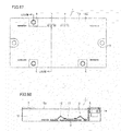
- lead frame 2 with semiconductor chip 11 mounted is set in a recessed portion 21 d of a first metal mold 21 , with a rear surface of heat-radiating plate 7 facing upward.
- lead frame 2 is set in such a manner that semiconductor chip 11 is covered with resin from above, or from the side on which semiconductor chip 11 is mounted.
- First metal mold 21 has a gate 21 a formed therein, for feeding resin to the recessed portion 21 d . Tip end portion of each lead terminal 4 and tip end portion of main electrode terminal 5 are inserted to reception openings 21 b provided in first metal mold 21 .
- a second metal mold 22 is mounted on the first metal mold 21 such that lead frame 2 set in recessed portion 21 d of first metal mold 21 is enclosed in recessed portion 21 d .
- resin 13 is introduced through gate 21 a , and recessed portion 21 d containing frame body 3 and the like therein is filled with resin 13 .
- a thermoplastic resin such as PPS (Poly Phenylene Sulfide) is used as the resin.
- second metal mold 22 is separated from first metal mold 21 .
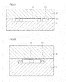
- a semiconductor device having semiconductor chip 11 and frame body 3 and the like (see FIG. 7 ) sealed with resin 13 as shown in FIG. 20 is taken out.
- a surface 13 a of resin 13 corresponding to the upper surface of the semiconductor device that is, the surface 13 a of resin 13 of that portion which covers semiconductor chip 11 from above, tip portions of lead terminal 4 and main electrode terminal 5 are exposed.
- a nut 14 for fixing a bus bar (not shown) or the like with a bolt is provided on the surface 13 a of resin 13 .
- main electrode terminal 5 and lead terminal 4 are exposed at surface 13 a of resin 13 , and lead terminal and the like are not exposed on any side surface.
- a surface (lower surface) of heat-radiating plate 7 is exposed.
- lead frame 2 (frame body 3 ) and semiconductor chip 11 as a whole mounted on the upper surface of heat-radiating plate 7 are covered with resin 13 from above, and sealed with resin 13 .
- main electrode terminal 5 and lead terminal 4 are not exposed at the side surface of resin 13 , and exposed at upper surface 13 a of resin 13 opposite to heat-radiating plate 7 . If lead terminal 4 and the like are protruded and exposed at the side surface of resin 13 , it would be necessary to ensure sufficient distance between the exposed portion of lead terminal 4 and the like and the exposed portion (lower surface) of heat-radiating plate 7 formed of metal, in order to prevent creeping discharge between these portions. Therefore, in that case, resin 13 must have a prescribed thickness.
- semiconductor chip 11 such as an IGBT or a diode has been described as an exemplary semiconductor chip to be mounted on frame body 3 of lead frame 2 . Specifically, only power semiconductors are described as examples.
- a control circuit chip 19 having a control circuit for controlling an operation of semiconductor device 1 formed thereon, may be mounted.
- control circuit (IC (Integrated Circuit)) chip 19 is sealed with resin, control circuit chip 19 is protected, and hence, reliability of driving semiconductor device 1 can be improved.
- a printed board 20 having an interconnection pattern allowing electrical connection with lead terminal 4 may be arranged at a prescribed position of an upper surface of resin 13 such as a portion where a recessed portion 13 b is formed, and on printed board 20 , a packaged control circuit (IC) 19 p or other electronic component may be mounted as shown in FIG. 25 .
- a lead terminal (pin) 26 for external connection, allowing signal input/output to/from control circuit (IC) 19 p or the like may be provided on printed board 20 , and for protection of printed board 20 or the like, printed board 20 or the like may be covered with a lid 25 or with resin (not shown).
- heat-radiating plate 7 As shown in FIGS. 26 and 27 , as a heat-radiating plate, heat-radiating plate 7 having openings 8 formed at opposite ends along the longitudinal direction is prepared. Then, through the similar method as described above, semiconductor chip 11 of IGBT or diode is adhered (die-bonded) to frame body 3 . Next, a prescribed electrode of the die-bonded semiconductor chip 11 and a corresponding lead terminal 4 or the like are electrically connected by a wire. Then, the tie bar portion is cut.
- lead frame 2 having semiconductor chip 11 mounted thereon is set with the rear surface of heat-radiating plate 7 facing upward, in recessed portion 21 d of first metal mold 21 .
- a second metal mold 22 is mounted on the first metal mold 21 such that lead frame 2 set in recessed portion 21 d of first metal mold 21 is enclosed in recessed portion 21 d .
- resin 13 is introduced through gate 21 a , and recessed portion 21 d containing frame body 3 and the like therein is filled with thermoplastic resin 13 (see, for example, FIG. 18 ).
- second metal mold 22 is separated from first metal mold 21 .
- main electrode terminal 5 is bent to be parallel to the upper surface 13 a of resin 13 .
- semiconductor device 1 is finished.
- heat-radiating plate 7 is provided with openings 8 , and resin 13 enters the openings 8 at the time of sealing with resin 13 .
- adhesion between resin 13 and heat-radiating plate 7 can be improved. Consequently, moisture resistance of semiconductor device 1 can be improved, and hence, reliability can further be improved.
- heat-radiating plate 7 having an openings formed at prescribed positions has been described as an example.
- heat-radiating plate 7 one having a trench may be used, besides the openings 8 .
- FIGS. 30 and 31 a heat-radiating plate 7 having trenches 9 formed at opposite ends along the longitudinal direction is prepared. Trenches 9 extend along the direction of introducing the resin.
- Lead frame 2 and semiconductor chip 11 are mounted on heat-radiating plate 7 , thereafter, as shown in FIG. 32 , lead frame 2 is set in recessed portion 21 d of first metal mold 21 , and second metal mold 22 is mounted on the first metal mold 21 .
- resin 13 (see, for example, FIG. 18 ) is introduced through gate 21 a , and recessed portion 21 d containing frame body 3 and the like therein is filled with thermoplastic resin 13 .
- resin 13 is introduced, trenches 9 formed along the direction of introduction are surely filled with resin.
- second metal mold 22 is separated from the first metal mold 21 , and the semiconductor device having semiconductor chip 11 , frame body 3 and the like sealed with resin 13 is taken out.
- main electrode terminal 5 is bent to be parallel to the upper surface 13 a of resin 13 as shown in FIG. 33 , and semiconductor device 1 is finished.
- trenches 9 are formed in heat-radiating plate 7 along the direction of introducing resin 13 . Therefore, the trenches can more reliably be filled with resin 13 when the resin is introduced, and hence, adhesion between resin 13 and heat-radiating plate 7 can be improved as in the case of openings 8 .
- an opening with a taper 8 a of which cross-sectional area is increased gradually from the front surface side to the rear surface side of heat-radiating plate 7 , such as shown in FIG. 34 , may be used.
- a trench 9 with a similar taper 9 a such as shown in FIG. 35 , may be used.
- Ceramic substrate 15 includes a ceramic substrate body 16 and a prescribed copper pattern 17 .
- the prescribed copper pattern 17 is formed both on a front surface and a rear surface of ceramic substrate body 16 .
- copper pattern 17 As to copper pattern 17 , on the surface of ceramic substrate body 16 on which the semiconductor chip is to be mounted (front surface), a copper pattern 17 a corresponding to arrangements of the semiconductor chip, lead terminal and the like is formed. On a prescribed position of copper pattern 17 a , semiconductor chip 11 is mounted (die-bonded) using solder 18 . On a rear surface of ceramic substrate body 16 , a copper pattern 17 b is formed, and fixed by solder 18 to a surface of heat-radiating plate 7 .
- lead frame 2 is attached such that lead terminal 4 and main electrode terminal 5 are connected to the corresponding copper pattern 17 a .
- Lead terminal 4 and main electrode terminal 5 are connected by solder to the corresponding copper pattern 17 a .
- semiconductor device 1 having semiconductor chip 11 and ceramic substrate 15 sealed with resin 13 is formed, as shown in FIGS. 39 and 40 .
- thermoplastic resin 13 thermoplastic resin 13
- main electrode terminal 5 and lead terminal 4 are exposed only at the upper surface 13 a of resin 13 opposite to heat-radiating plate 7 . Accordingly, thickness of resin 13 can be reduced as described above, which contributes to reduction in size of semiconductor device 1 . Further, as the ceramic substrate is used, semiconductor device 1 comes to have good heat-radiating property.
- a semiconductor device having a ceramic substrate fixed on a heat-radiating plate has been described as an example.
- the device may not include a heat-radiating plate.
- semiconductor chip 11 is mounted (die-bonded) using solder 18 .
- copper pattern 17 b on the rear surface of ceramic substrate 16 no heat-radiating plate is fixed, and copper pattern 17 b is exposed.
- lead frame 2 is attached such that lead terminal 4 and main electrode terminal 5 are connected to corresponding copper pattern 17 a .
- Lead terminal 4 and main electrode terminal 5 are connected by solder to the corresponding copper pattern 17 a .
- semiconductor device 1 having semiconductor chip 11 and ceramic substrate 15 (see FIG. 43 ) sealed with resin 13 is formed, as shown in FIGS. 44 and 45 .
- lead frame 2 as the element-mounting member is prepared.
- Lead frame 2 is punched out to a prescribed pattern to provide a portion of frame body 3 on which a semiconductor chip is mounted, a portion to be a lead terminal 4 , and a portion to be a main electrode terminal 5 . These portions are connected to each other by a tie bar 6 .
- a semiconductor chip 11 such as an IGBT or a diode is adhered with solder at a prescribed position of frame body 3 (die-bonding).
- a prescribed electrode of die-bonded semiconductor chip 11 and a corresponding lead terminal 4 or the like are electrically connected by a prescribed wire 12 (wire-bonding).
- portions to be lead terminal 4 and main electrode terminal 5 of lead frame 2 are bent upward with respect to frame body 3 .
- lead frame 2 is set in a recessed portion 21 d of a first metal mold 21 , with a rear surface of frame body 3 , having semiconductor chip 11 mounted, facing upward.
- tip end portions of lead terminal 4 and main electrode terminal 5 are inserted to reception openings 21 b provided in first metal mold 21 .
- first metal mold 21 lead terminals 4 are tied by tie bar 6 , and therefore, there is provided an opening 21 c to which a prescribed sliding mold 23 is inserted to prevent the flow of resin.
- a similar opening (not shown) corresponding to the shape of lead frame 2 is formed also on a side surface opposite to the side surface having opening 21 c formed therein, and the corresponding sliding mold (not shown) is inserted to the opening.
- second metal mold 22 is mounted on the first metal mold 21 such that lead frame 2 set in recessed portion of first metal mold 21 is enclosed in recessed portion 21 d . Then, sliding mold 23 is inserted to opening 21 c of the first metal mold 21 .
- thermoplastic resin 31 is introduced through gate 21 a , and recessed portion 21 d containing frame body 3 and the like is filled with resin 13 .
- the second metal mold 22 is separated from the first metal mold 21 .
- semiconductor device 1 having semiconductor chip 11 , frame body 3 and the like sealed with resin 13 is taken out, as shown in FIG. 65 . From the surface 13 a of resin 13 that corresponds to the upper surface of semiconductor device 1 , lead terminal 4 , main electrode terminal 5 and tie bar 6 connecting these are exposed.
- tie bar 6 is cut, and as shown in FIGS. 66 , 67 and 68 , main electrode terminal 5 is bent to be parallel to the upper surface of resin 13 , whereby semiconductor device 1 is finished.
- main electrode terminal 5 and lead terminal 4 are exposed at the surface of resin 13 , and the lead terminal and the like are not exposed at the side surface of resin 13 .
- cross sections of cut tie bar 6 are exposed at the surface 13 a of resin 13 .
- the semiconductor device according to the present invention may be effectively utilized as a semiconductor device for driving an inverter of industrial equipment and the like.
Abstract
Description
Claims (3)
Priority Applications (1)
| Application Number | Priority Date | Filing Date | Title |
|---|---|---|---|
| US13/007,286 US8093692B2 (en) | 2007-03-26 | 2011-01-14 | Semiconductor device packaging including a power semiconductor element |
Applications Claiming Priority (4)
| Application Number | Priority Date | Filing Date | Title |
|---|---|---|---|
| JP2007-079684 | 2007-03-26 | ||
| JP2007079684A JP5252819B2 (en) | 2007-03-26 | 2007-03-26 | Semiconductor device and manufacturing method thereof |
| US11/834,902 US7892893B2 (en) | 2007-03-26 | 2007-08-07 | Semiconductor device and manufacturing method thereof |
| US13/007,286 US8093692B2 (en) | 2007-03-26 | 2011-01-14 | Semiconductor device packaging including a power semiconductor element |
Related Parent Applications (1)
| Application Number | Title | Priority Date | Filing Date |
|---|---|---|---|
| US11/834,902 Division US7892893B2 (en) | 2007-03-26 | 2007-08-07 | Semiconductor device and manufacturing method thereof |
Publications (2)
| Publication Number | Publication Date |
|---|---|
| US20110108964A1 US20110108964A1 (en) | 2011-05-12 |
| US8093692B2 true US8093692B2 (en) | 2012-01-10 |
Family
ID=39914980
Family Applications (2)
| Application Number | Title | Priority Date | Filing Date |
|---|---|---|---|
| US11/834,902 Active 2029-02-27 US7892893B2 (en) | 2007-03-26 | 2007-08-07 | Semiconductor device and manufacturing method thereof |
| US13/007,286 Active US8093692B2 (en) | 2007-03-26 | 2011-01-14 | Semiconductor device packaging including a power semiconductor element |
Family Applications Before (1)
| Application Number | Title | Priority Date | Filing Date |
|---|---|---|---|
| US11/834,902 Active 2029-02-27 US7892893B2 (en) | 2007-03-26 | 2007-08-07 | Semiconductor device and manufacturing method thereof |
Country Status (4)
| Country | Link |
|---|---|
| US (2) | US7892893B2 (en) |
| JP (1) | JP5252819B2 (en) |
| KR (1) | KR100909060B1 (en) |
| CN (1) | CN101276799B (en) |
Cited By (7)
| Publication number | Priority date | Publication date | Assignee | Title |
|---|---|---|---|---|
| US20130221516A1 (en) * | 2011-02-09 | 2013-08-29 | Mitsubishi Electric Corporation | Power semiconductor module |
| US20140313675A1 (en) * | 2013-04-19 | 2014-10-23 | Hyundai Autron Co., Ltd. | Electronic control apparatus for vehicle using overmolding and manufacturing method thereof |
| US20150009629A1 (en) * | 2013-07-05 | 2015-01-08 | Hyundai Autron Co., Ltd. | Electronic control apparatus for vehicle using radiation board and manufacturing method thereof |
| USD731491S1 (en) * | 2014-02-07 | 2015-06-09 | NimbeLink L.L.C. | Embedded cellular modem |
| USD759604S1 (en) * | 2015-06-17 | 2016-06-21 | Mitsubishi Electric Corporation | Semiconductor device |
| USD761746S1 (en) * | 2014-11-04 | 2016-07-19 | Sumitomo Electric Industries, Ltd. | Semiconductor module for power conversion |
| US9497570B2 (en) | 2014-02-06 | 2016-11-15 | Nimbelink Corp. | Embedded wireless modem |
Families Citing this family (30)
| Publication number | Priority date | Publication date | Assignee | Title |
|---|---|---|---|---|
| EP2120263A4 (en) * | 2007-11-30 | 2010-10-13 | Panasonic Corp | Heat dissipating structure base board, module using heat dissipating structure base board, and method for manufacturing heat dissipating structure base board |
| JP5106519B2 (en) | 2009-11-19 | 2012-12-26 | Necアクセステクニカ株式会社 | Thermally conductive substrate and electronic component mounting method thereof |
| JP4947135B2 (en) * | 2009-12-04 | 2012-06-06 | 株式会社デンソー | Semiconductor package and manufacturing method thereof |
| JP5500718B2 (en) * | 2010-03-05 | 2014-05-21 | 株式会社ケーヒン | Semiconductor device |
| JP5319601B2 (en) | 2010-05-10 | 2013-10-16 | 株式会社東芝 | Semiconductor device and power semiconductor device |
| JP5253455B2 (en) * | 2010-06-01 | 2013-07-31 | 三菱電機株式会社 | Power semiconductor device |
| JP5936310B2 (en) * | 2011-03-17 | 2016-06-22 | 三菱電機株式会社 | Power semiconductor module and its mounting structure |
| ITMI20111208A1 (en) | 2011-06-30 | 2012-12-31 | St Microelectronics Srl | SYSTEM WITH STABILIZED HEAT SINK |
| ITMI20111217A1 (en) | 2011-06-30 | 2012-12-31 | St Microelectronics Srl | CONTAINER / SINK SYSTEM FOR ELECTRONIC COMPONENT |
| ITMI20111213A1 (en) | 2011-06-30 | 2012-12-31 | St Microelectronics Srl | SEMI-BRIDGE ELECTRONIC DEVICE WITH COMMON AUXILIARY HEAT SINK |
| ITMI20111214A1 (en) | 2011-06-30 | 2012-12-31 | St Microelectronics Srl | POWER REDUCED THICKNESS DEVICE |
| ITMI20111218A1 (en) | 2011-06-30 | 2012-12-31 | St Microelectronics Srl | HIGH SPEED POWER DEVICE? OF SWITCHING |
| ITMI20111219A1 (en) * | 2011-06-30 | 2012-12-31 | St Microelectronics Srl | SYSTEM WITH SHARED HEAT SINK |
| ITMI20111216A1 (en) | 2011-06-30 | 2012-12-31 | St Microelectronics Srl | ELECTRONIC POWER DEVICE WITH HIGH HEAT DISSIPATION AND STABILITY? |
| DE102012215656B4 (en) * | 2012-09-04 | 2015-05-21 | Semikron Elektronik Gmbh & Co. Kg | Method for producing a power semiconductor module |
| JP2014056982A (en) * | 2012-09-13 | 2014-03-27 | Mitsubishi Electric Corp | Power semiconductor device and manufacturing method of the same |
| JP6368646B2 (en) | 2012-09-20 | 2018-08-01 | ローム株式会社 | Power module semiconductor device, inverter device, power module semiconductor device manufacturing method, and mold |
| DE102012222959B4 (en) * | 2012-12-12 | 2015-04-02 | Semikron Elektronik Gmbh & Co. Kg | Power component device |
| JP2014146704A (en) * | 2013-01-29 | 2014-08-14 | Fuji Electric Co Ltd | Semiconductor device |
| WO2015045648A1 (en) * | 2013-09-30 | 2015-04-02 | 富士電機株式会社 | Semiconductor device, method for assembling semiconductor device, component for semiconductor devices and unit module |
| JP2015179690A (en) * | 2014-03-18 | 2015-10-08 | 三菱電機株式会社 | Transistor chip and semiconductor apparatus |
| CN112652543B (en) * | 2015-10-06 | 2023-12-26 | 三菱电机株式会社 | Method for manufacturing semiconductor device |
| US10438865B2 (en) * | 2016-02-04 | 2019-10-08 | Mitsubishi Electric Corporation | Semiconductor device |
| JP6673012B2 (en) * | 2016-05-26 | 2020-03-25 | 三菱電機株式会社 | Semiconductor device and manufacturing method thereof |
| US10074590B1 (en) * | 2017-07-02 | 2018-09-11 | Infineon Technologies Ag | Molded package with chip carrier comprising brazed electrically conductive layers |
| EP3703118B1 (en) * | 2017-10-26 | 2022-05-18 | Shindengen Electric Manufacturing Co., Ltd. | Semiconductor device |
| DE102020207686A1 (en) | 2020-06-22 | 2021-12-23 | Zf Friedrichshafen Ag | Power module for operating an electric vehicle drive with optimized cooling and contacting |
| JP7352753B2 (en) | 2020-10-14 | 2023-09-28 | ローム株式会社 | semiconductor module |
| WO2022080122A1 (en) | 2020-10-14 | 2022-04-21 | ローム株式会社 | Semiconductor module |
| DE202021004370U1 (en) | 2020-10-14 | 2023-12-12 | Rohm Co., Ltd. | Semiconductor module |
Citations (32)
| Publication number | Priority date | Publication date | Assignee | Title |
|---|---|---|---|---|
| US4639759A (en) * | 1982-11-10 | 1987-01-27 | Brown, Boveri & Cie., Ag | Power transistor module |
| US4942455A (en) | 1986-10-13 | 1990-07-17 | Mitsubishi Denki Kabushiki Kaisha | Lead frame for a semiconductor device and a method for manufacturing a semiconductor device using the lead frame |
| US5519252A (en) * | 1992-07-24 | 1996-05-21 | Fuji Electric Co., Ltd. | Power semiconductor device employing pin block connection arrangement for facilitated and economized manufacture |
| US5559374A (en) * | 1993-03-25 | 1996-09-24 | Sanyo Electric Co., Ltd. | Hybrid integrated circuit |
| JPH09232512A (en) | 1996-02-22 | 1997-09-05 | Hitachi Ltd | Power semiconductor module |
| US5666003A (en) | 1994-10-24 | 1997-09-09 | Rohm Co. Ltd. | Packaged semiconductor device incorporating heat sink plate |
| US5698898A (en) * | 1995-12-21 | 1997-12-16 | Mitsubishi Denki Kabushiki Kaisha | Semiconductor apparatus with a multiple element electrode structure |
| JPH1022435A (en) | 1996-07-02 | 1998-01-23 | Hitachi Ltd | Semiconductor device and manufacture thereof |
| JPH10135380A (en) | 1996-10-31 | 1998-05-22 | Hitachi Ltd | Semiconductor device |
| US5763946A (en) | 1995-07-26 | 1998-06-09 | Kabushiki Kaisha Toshiba | Semiconductor device with bent electrode terminal |
| KR19980021184A (en) | 1996-09-13 | 1998-06-25 | 김광호 | Semiconductor chip package with heat sink |
| US5825085A (en) * | 1995-09-01 | 1998-10-20 | Mitsubishi Denki Kabushiki Kaisha | Power semiconductor device, armoring case thereof and method for manufacturing the same |
| JP2000323646A (en) | 1999-05-14 | 2000-11-24 | Mitsubishi Electric Corp | Insulating material case and semiconductor device |
| US6291880B1 (en) | 1998-02-12 | 2001-09-18 | Hitachi, Ltd. | Semiconductor device including an integrally molded lead frame |
| US6313598B1 (en) | 1998-09-11 | 2001-11-06 | Hitachi, Ltd. | Power semiconductor module and motor drive system |
| US20010052639A1 (en) | 2000-06-13 | 2001-12-20 | Fairchild Korea Semiconductor Ltd. | Power module package having insulator type heat sink attached to rear surface of lead frame and manufacturing method thereof |
| US6369411B2 (en) * | 1999-05-11 | 2002-04-09 | Mitsubishi Denki Kabushiki Kaisha | Semiconductor device for controlling high-power electricity with improved heat dissipation |
| KR20020036007A (en) | 2000-11-07 | 2002-05-16 | 김덕중 | Power module package having improved heat transfer performance |
| US20020145195A1 (en) | 1999-03-16 | 2002-10-10 | Kazutaka Okamoto | Composite material, and manufacturing method and uses of same |
| JP2002314038A (en) | 2001-04-18 | 2002-10-25 | Hitachi Ltd | Power semiconductor module |
| US20020190374A1 (en) | 2001-06-19 | 2002-12-19 | Mitsubishi Denki Kabushiki Kaisha | Semiconductor device |
| US6521983B1 (en) * | 2000-08-29 | 2003-02-18 | Mitsubishi Denki Kabushiki Kaisha | Semiconductor device for electric power |
| US6597063B1 (en) | 1997-12-08 | 2003-07-22 | Kabushiki Kaisha Toshiba | Package for semiconductor power device and method for assembling the same |
| US6727585B2 (en) | 2001-05-04 | 2004-04-27 | Ixys Corporation | Power device with a plastic molded package and direct bonded substrate |
| US6809410B2 (en) * | 2000-11-30 | 2004-10-26 | Mitsubishi Denki Kabushiki Kaisha | Power semiconductor module |
| US20040227231A1 (en) | 2003-05-16 | 2004-11-18 | Ballard Power Systems Corporation | Power module with voltage overshoot limiting |
| US6873042B2 (en) | 2001-04-02 | 2005-03-29 | Mitsubishi Denki Kabushiki Kaisha | Plurality of power elements with gate interconnections having equal lengths |
| US20050199999A1 (en) | 2004-03-09 | 2005-09-15 | Mitsubishi Denki Kabushiki Kaisha | Semiconductor device |
| US6979843B2 (en) * | 2002-03-08 | 2005-12-27 | Mitsubishi Denki Kabushiki Kaisha | Power semiconductor device |
| US7074654B1 (en) | 2004-04-21 | 2006-07-11 | Amkor Technology, Inc. | Tape supported memory card leadframe structure |
| US20070138624A1 (en) * | 2005-12-19 | 2007-06-21 | Mitsubishi Electric Corporation | Semiconductor device |
| US20070215999A1 (en) | 2006-03-03 | 2007-09-20 | Mitsubishi Electric Corporation | Semiconductor device |
Family Cites Families (5)
| Publication number | Priority date | Publication date | Assignee | Title |
|---|---|---|---|---|
| JPH04277660A (en) * | 1991-03-06 | 1992-10-02 | Nec Corp | Integrated circuit package |
| JP3345241B2 (en) * | 1995-11-30 | 2002-11-18 | 三菱電機株式会社 | Semiconductor device |
| JP3491481B2 (en) * | 1996-08-20 | 2004-01-26 | 株式会社日立製作所 | Semiconductor device and manufacturing method thereof |
| KR100246587B1 (en) * | 1997-09-19 | 2000-03-15 | 유무성 | Ball grid array semiconductor package |
| JP4722415B2 (en) * | 2004-06-14 | 2011-07-13 | 三菱電機株式会社 | Semiconductor device and manufacturing method thereof |
-
2007
- 2007-03-26 JP JP2007079684A patent/JP5252819B2/en active Active
- 2007-08-07 US US11/834,902 patent/US7892893B2/en active Active
- 2007-10-05 KR KR1020070100285A patent/KR100909060B1/en active IP Right Grant
- 2007-10-15 CN CN2007101524945A patent/CN101276799B/en active Active
-
2011
- 2011-01-14 US US13/007,286 patent/US8093692B2/en active Active
Patent Citations (35)
| Publication number | Priority date | Publication date | Assignee | Title |
|---|---|---|---|---|
| US4639759A (en) * | 1982-11-10 | 1987-01-27 | Brown, Boveri & Cie., Ag | Power transistor module |
| US4942455A (en) | 1986-10-13 | 1990-07-17 | Mitsubishi Denki Kabushiki Kaisha | Lead frame for a semiconductor device and a method for manufacturing a semiconductor device using the lead frame |
| US5519252A (en) * | 1992-07-24 | 1996-05-21 | Fuji Electric Co., Ltd. | Power semiconductor device employing pin block connection arrangement for facilitated and economized manufacture |
| US5559374A (en) * | 1993-03-25 | 1996-09-24 | Sanyo Electric Co., Ltd. | Hybrid integrated circuit |
| US5666003A (en) | 1994-10-24 | 1997-09-09 | Rohm Co. Ltd. | Packaged semiconductor device incorporating heat sink plate |
| US5763946A (en) | 1995-07-26 | 1998-06-09 | Kabushiki Kaisha Toshiba | Semiconductor device with bent electrode terminal |
| US5825085A (en) * | 1995-09-01 | 1998-10-20 | Mitsubishi Denki Kabushiki Kaisha | Power semiconductor device, armoring case thereof and method for manufacturing the same |
| US5698898A (en) * | 1995-12-21 | 1997-12-16 | Mitsubishi Denki Kabushiki Kaisha | Semiconductor apparatus with a multiple element electrode structure |
| US5920119A (en) * | 1996-02-22 | 1999-07-06 | Hitachi, Ltd. | Power semiconductor module employing metal based molded case and screw fastening type terminals for high reliability |
| JPH09232512A (en) | 1996-02-22 | 1997-09-05 | Hitachi Ltd | Power semiconductor module |
| JPH1022435A (en) | 1996-07-02 | 1998-01-23 | Hitachi Ltd | Semiconductor device and manufacture thereof |
| KR19980021184A (en) | 1996-09-13 | 1998-06-25 | 김광호 | Semiconductor chip package with heat sink |
| JPH10135380A (en) | 1996-10-31 | 1998-05-22 | Hitachi Ltd | Semiconductor device |
| US6597063B1 (en) | 1997-12-08 | 2003-07-22 | Kabushiki Kaisha Toshiba | Package for semiconductor power device and method for assembling the same |
| US6291880B1 (en) | 1998-02-12 | 2001-09-18 | Hitachi, Ltd. | Semiconductor device including an integrally molded lead frame |
| US6313598B1 (en) | 1998-09-11 | 2001-11-06 | Hitachi, Ltd. | Power semiconductor module and motor drive system |
| US20020145195A1 (en) | 1999-03-16 | 2002-10-10 | Kazutaka Okamoto | Composite material, and manufacturing method and uses of same |
| US6369411B2 (en) * | 1999-05-11 | 2002-04-09 | Mitsubishi Denki Kabushiki Kaisha | Semiconductor device for controlling high-power electricity with improved heat dissipation |
| JP2000323646A (en) | 1999-05-14 | 2000-11-24 | Mitsubishi Electric Corp | Insulating material case and semiconductor device |
| US20010052639A1 (en) | 2000-06-13 | 2001-12-20 | Fairchild Korea Semiconductor Ltd. | Power module package having insulator type heat sink attached to rear surface of lead frame and manufacturing method thereof |
| US6521983B1 (en) * | 2000-08-29 | 2003-02-18 | Mitsubishi Denki Kabushiki Kaisha | Semiconductor device for electric power |
| KR20020036007A (en) | 2000-11-07 | 2002-05-16 | 김덕중 | Power module package having improved heat transfer performance |
| US6809410B2 (en) * | 2000-11-30 | 2004-10-26 | Mitsubishi Denki Kabushiki Kaisha | Power semiconductor module |
| US6873042B2 (en) | 2001-04-02 | 2005-03-29 | Mitsubishi Denki Kabushiki Kaisha | Plurality of power elements with gate interconnections having equal lengths |
| JP2002314038A (en) | 2001-04-18 | 2002-10-25 | Hitachi Ltd | Power semiconductor module |
| US6727585B2 (en) | 2001-05-04 | 2004-04-27 | Ixys Corporation | Power device with a plastic molded package and direct bonded substrate |
| US20020190374A1 (en) | 2001-06-19 | 2002-12-19 | Mitsubishi Denki Kabushiki Kaisha | Semiconductor device |
| US6700194B2 (en) * | 2001-06-19 | 2004-03-02 | Mitsubishi Denki Kabushiki Kaisha | Semiconductor device |
| US6979843B2 (en) * | 2002-03-08 | 2005-12-27 | Mitsubishi Denki Kabushiki Kaisha | Power semiconductor device |
| US20040227231A1 (en) | 2003-05-16 | 2004-11-18 | Ballard Power Systems Corporation | Power module with voltage overshoot limiting |
| US20050199999A1 (en) | 2004-03-09 | 2005-09-15 | Mitsubishi Denki Kabushiki Kaisha | Semiconductor device |
| US7074654B1 (en) | 2004-04-21 | 2006-07-11 | Amkor Technology, Inc. | Tape supported memory card leadframe structure |
| US20070138624A1 (en) * | 2005-12-19 | 2007-06-21 | Mitsubishi Electric Corporation | Semiconductor device |
| US20070215999A1 (en) | 2006-03-03 | 2007-09-20 | Mitsubishi Electric Corporation | Semiconductor device |
| US7589412B2 (en) * | 2006-03-03 | 2009-09-15 | Mitsubishi Electric Corporation | Semiconductor device |
Cited By (10)
| Publication number | Priority date | Publication date | Assignee | Title |
|---|---|---|---|---|
| US20130221516A1 (en) * | 2011-02-09 | 2013-08-29 | Mitsubishi Electric Corporation | Power semiconductor module |
| US9129949B2 (en) * | 2011-02-09 | 2015-09-08 | Mitsubishi Electric Corporation | Power semiconductor module |
| US20140313675A1 (en) * | 2013-04-19 | 2014-10-23 | Hyundai Autron Co., Ltd. | Electronic control apparatus for vehicle using overmolding and manufacturing method thereof |
| US9313932B2 (en) * | 2013-04-19 | 2016-04-12 | Hyundai Autron Co., Ltd. | Electronic control apparatus for vehicle using overmolding and manufacturing method thereof |
| US20150009629A1 (en) * | 2013-07-05 | 2015-01-08 | Hyundai Autron Co., Ltd. | Electronic control apparatus for vehicle using radiation board and manufacturing method thereof |
| US9185831B2 (en) * | 2013-07-05 | 2015-11-10 | Hyundai Autron Co., Ltd. | Electronic control apparatus for vehicle using radiation board and manufacturing method thereof |
| US9497570B2 (en) | 2014-02-06 | 2016-11-15 | Nimbelink Corp. | Embedded wireless modem |
| USD731491S1 (en) * | 2014-02-07 | 2015-06-09 | NimbeLink L.L.C. | Embedded cellular modem |
| USD761746S1 (en) * | 2014-11-04 | 2016-07-19 | Sumitomo Electric Industries, Ltd. | Semiconductor module for power conversion |
| USD759604S1 (en) * | 2015-06-17 | 2016-06-21 | Mitsubishi Electric Corporation | Semiconductor device |
Also Published As
| Publication number | Publication date |
|---|---|
| CN101276799B (en) | 2010-06-02 |
| KR100909060B1 (en) | 2009-07-23 |
| JP5252819B2 (en) | 2013-07-31 |
| US7892893B2 (en) | 2011-02-22 |
| KR20080087632A (en) | 2008-10-01 |
| US20110108964A1 (en) | 2011-05-12 |
| JP2008243970A (en) | 2008-10-09 |
| CN101276799A (en) | 2008-10-01 |
| US20080283983A1 (en) | 2008-11-20 |
Similar Documents
| Publication | Publication Date | Title |
|---|---|---|
| US8093692B2 (en) | Semiconductor device packaging including a power semiconductor element | |
| US5703399A (en) | Semiconductor power module | |
| EP2605276B1 (en) | Packaged leadless semiconductor device | |
| KR100403608B1 (en) | Stacked intelligent power module package and manufacturing method thereof | |
| US5172214A (en) | Leadless semiconductor device and method for making the same | |
| US5616957A (en) | Plastic package type semiconductor device | |
| US10950516B2 (en) | Resin encapsulated power semiconductor module with exposed terminal areas | |
| US8198712B2 (en) | Hermetically sealed semiconductor device module | |
| US20100013070A1 (en) | Power module package having excellent heat sink emission capability and method for manufacturing the same | |
| US20030113954A1 (en) | Method of making a semiconductor package having exposed metal strap | |
| US6710439B2 (en) | Three-dimensional power semiconductor module and method of manufacturing the same | |
| US5309322A (en) | Leadframe strip for semiconductor packages and method | |
| EP3577684B1 (en) | Power semiconductor module | |
| KR101555300B1 (en) | Semiconductor power module package having external boding area | |
| US7745257B2 (en) | High power MCM package with improved planarity and heat dissipation | |
| US7808088B2 (en) | Semiconductor device with improved high current performance | |
| CN115443531A (en) | Power module, manufacturing method thereof, converter and electronic equipment | |
| US20230027138A1 (en) | Power module | |
| JP2003197828A (en) | Resin-sealing semiconductor device | |
| KR100195511B1 (en) | Ball grid array package using leadframe | |
| KR101016715B1 (en) | Semiconductor device | |
| KR0134816Y1 (en) | Multiside package | |
| JPH08255853A (en) | Electronic component mounting device | |
| KR19980025623A (en) | Semiconductor package | |
| KR20180049415A (en) | Power module and the method of packaging of the same |
Legal Events
| Date | Code | Title | Description |
|---|---|---|---|
| FEPP | Fee payment procedure |
Free format text: PAYOR NUMBER ASSIGNED (ORIGINAL EVENT CODE: ASPN); ENTITY STATUS OF PATENT OWNER: LARGE ENTITY |
|
| STCF | Information on status: patent grant |
Free format text: PATENTED CASE |
|
| FPAY | Fee payment |
Year of fee payment: 4 |
|
| MAFP | Maintenance fee payment |
Free format text: PAYMENT OF MAINTENANCE FEE, 8TH YEAR, LARGE ENTITY (ORIGINAL EVENT CODE: M1552); ENTITY STATUS OF PATENT OWNER: LARGE ENTITY Year of fee payment: 8 |
|
| MAFP | Maintenance fee payment |
Free format text: PAYMENT OF MAINTENANCE FEE, 12TH YEAR, LARGE ENTITY (ORIGINAL EVENT CODE: M1553); ENTITY STATUS OF PATENT OWNER: LARGE ENTITY Year of fee payment: 12 |