US8068622B2 - Method and apparatus for controlling a selectable voltage audio power output stage - Google Patents
Method and apparatus for controlling a selectable voltage audio power output stage Download PDFInfo
- Publication number
- US8068622B2 US8068622B2 US11/611,069 US61106906A US8068622B2 US 8068622 B2 US8068622 B2 US 8068622B2 US 61106906 A US61106906 A US 61106906A US 8068622 B2 US8068622 B2 US 8068622B2
- Authority
- US
- United States
- Prior art keywords
- signal
- power supply
- audio
- magnitude
- supply voltage
- Prior art date
- Legal status (The legal status is an assumption and is not a legal conclusion. Google has not performed a legal analysis and makes no representation as to the accuracy of the status listed.)
- Active, expires
Links
Images


Classifications
-
- H—ELECTRICITY
- H03—ELECTRONIC CIRCUITRY
- H03F—AMPLIFIERS
- H03F1/00—Details of amplifiers with only discharge tubes, only semiconductor devices or only unspecified devices as amplifying elements
- H03F1/02—Modifications of amplifiers to raise the efficiency, e.g. gliding Class A stages, use of an auxiliary oscillation
- H03F1/0205—Modifications of amplifiers to raise the efficiency, e.g. gliding Class A stages, use of an auxiliary oscillation in transistor amplifiers
- H03F1/0211—Modifications of amplifiers to raise the efficiency, e.g. gliding Class A stages, use of an auxiliary oscillation in transistor amplifiers with control of the supply voltage or current
- H03F1/0244—Stepped control
- H03F1/025—Stepped control by using a signal derived from the input signal
Definitions
- the present invention relates generally to consumer device audio power output stages, and more specifically, to a control circuit for selecting the power supply voltage of an audio power stage.
- the power amplifier output which is generally utilized to drive a pair of headphones or a speaker can be the primary consumer of battery power.
- power is wasted during low signal level outputs, since the voltage drop across the active output transistor plus the output voltage will be equal to the constant power supply rail voltage. Even though the current in the transducer is reduced at low signal amplitudes, more power is still wasted by dissipation in the output transistors than is delivered to the load.
- Battery power is typically only reduced in linear amplifier circuits by lowering the power supply voltage, which limits the available output power and also may not be possible in some applications in which the power amplifier output also serves as a line output signal that must provide a specified signal level at full signal level, for example +5 dBm (15 dB over ⁇ 10 dBm) as referenced into a 600 ohm load, which requires a signal swing of 3 V p-p .
- the power amplifier circuit includes a power supply that has a selectable power supply output voltage, so that the amplifier power supply rail voltage can be lowered to reduce power consumption and decrease power dissipation when the maximum power supply voltage is not needed to amplify an audio signal.
- the power supply voltage is selected in conformity with an indication of magnitude of the audio signal.
- a control circuit that selects the power supply output voltage controls the volume of the signal as well, either with an audio compressor that is enabled until the power supply voltage has stabilized at a higher voltage level, or by delaying an increase in volume due to a volume control setting.
- the control circuit provides the indication of magnitude from an upstream source of the audio signal such as a decoder or filter, such that the indication of magnitude is provided in sufficient advance of peaks in the audio signal at the amplifier so that the power supply can stabilize at a higher operating voltage before arrival of the peaks at the amplifier.
- FIG. 1 is a schematic diagram depicting an audio output stage of a consumer audio device in accordance with an embodiment of the invention.
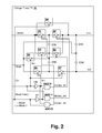
- FIG. 2 is a schematic diagram depicting charge-pump power supply 10 of FIG. 1 .
- FIGS. 3A-3D are schematic diagrams depicting the individual charge-pump clock phases for each operating mode of the charge-pump power supply circuit of FIG. 2 .
- FIG. 4 is a schematic diagram depicting an amplifier control circuit in accordance with an embodiment of the invention.
- FIG. 5 is a schematic diagram depicting amplifier power supply control mechanisms in accordance with an embodiment of the invention.
- the present invention encompasses a control method and apparatus for selecting a power supply voltage supplied to an audio power amplifier.
- the voltage of the power supply provided to the final power amplifier stage is selectable and is set in conformity with either an expected or actual signal level of the audio signal being amplified, so that at signal amplitudes that do not require the maximum power supply voltage, the power supply voltage is reduced to conserve power. For example, when amplifying a signal having typical maximum amplitude ⁇ 6 dB below occasional peaks referenced at 0 dB, the power supply voltage of the final amplifier stage can be reduced by a factor of two during intervals between the above-described peaks, without causing clipping.
- the result is a potential reduction in power consumption by a factor of four and a reduction in power dissipation by at least that factor over that of an amplifier that does not have a selectable power supply.
- the control mechanism that select the power supply voltage either delays or suppresses increases in signal volume until a higher selected power supply voltage has stabilized, or receives signal amplitude information from an upstream source in sufficient advance that the power supply has time to stabilize at the higher voltage value before signal peaks arrive.
- a digital-to-analog converter (DAC) 14 supplies an analog signal to a first amplifier stage A 2 that is operated from a fixed voltage power supply.
- the input to DAC 14 may optionally be provided by a decoder 13 , that decodes a file or stream data source such as an MP3 encoded data stream.
- the signal at the output of first amplifier stage A 2 is provided to an attenuator 16 that receives a volume control signal and attenuates the signal accordingly.
- Attenuator 16 may be a digital potentiometer having control provided from a microcontroller or other digital control circuit responsive to a user interface, volume knob encoder or program command, or attenuator 16 may be an analog potentiometer that provides the volume control signal as an output indication from a secondary deck (separate potentiometer circuit coupled to the common shaft or other mechanism) for use in the power supply control algorithms described below. While an attenuator 16 is shown as the volume control mechanism, it is understood that an equivalent volume control may be provided by a programmable resistor in the feedback of amplifier A 2 or another amplifier stage in the signal path.
- a final power amplifier stage A 2 amplifies the signal received from attenuator 16 and provides an audio output signal, which may operate a speaker, headphone transducer, and/or a line level signal output.
- a capacitor C 1 may be utilized to couple the output signal to the transducer or line level output, particularly if amplifier A 1 is operated from a unipolar power supply having a quiescent voltage substantially differing from ground.
- the volume control signal is also supplied to a mode control circuit 12 for controlling the output power supply voltage supplied to the power supply rails of power amplifier A 1 in conformity with an expected range of signal levels at the output of power amplifier A 1 , so that power amplifier A 1 will not clip for high (peak) signal levels, but will have a reduced power supply voltage when high (peak) signal levels are not present.
- the output of amplifier A 2 is also provided to mode control circuit 12 so that actual signal levels can be measured by mode control circuit 12 and the power supply voltage of power amplifier A 1 adjusted in conformity with the actual signal level that will be reproduced at the output power amplifier A 1 .
- the volume control since the volume control is applied after the signal level measurement taken from the output of amplifier A 2 , the volume information is needed even if the signal level is detected by mode control circuit 12 , since mode control circuit must also receive information relating to the amount of gain/attenuation that will be applied to the signal prior to amplification by power amplifier A 1 .
- an output of decoder 13 if present, may provide an advance notification to mode control circuit 12 that a peak in signal amplitude will be arriving at DAC 14 and thus provide an early indication that the operating mode needs to be changed if the lower voltage/power operating mode of charge pump power supply 10 is selected.
- Charge pump power supply 10 provides the power supply rail inputs of amplifier A 1 and receives a power supply input, generally from a battery or other power supply, depicted as battery terminal connections Vbatt+ and Vbatt ⁇ .
- Mode control circuit 12 supplies a Mode Select signal to charge pump power supply 10 , that selects an operating mode of charge pump power supply 10 .
- Charge pump power supply 10 provides output power supply rail connections out+ and out ⁇ that will have a “full” (maximum) voltage in a first operating mode and a voltage that is a rational fraction of the full voltage in a second operating mode, as selected by mode control circuit, when the audio signal level is low enough or expected to be low enough that clipping will not occur at the output of power amplifier A 1 .
- FIG. 2 and additionally with reference to FIGS. 3A-3D , details of charge pump power supply 10 are shown.
- Mode 1 When the first operating mode (Mode 1 ) is selected, the Mode Select signal is in the logical high (“1”) state, and switch S 8 is closed, to apply the Vbatt+ voltage directly to the out+ terminal.
- FIG. 3A and FIG. 3B show the circuit connection arrangement for Mode 1 in the first and second clock phases, respectively, omitting open switches and inactive circuit components.
- Switches S 1 , S 2 and S 4 are open and not activated in the first operating mode, as logical AND gates AND 10 and AND 11 disable the control signals to switches S 1 , S 2 and S 4 , as the inverted Mode Select signal provided by inverter I 10 is in a logical low (“0”) state.
- capacitors C 12 -C 13 , switches S 3 , S 6 and switch S 7 are omitted.
- the positive power supply voltage at terminal out+ is supplied directly from the positive input terminal Vbatt+.
- the input voltage provided between input terminals Vbatt+ and Vbatt ⁇ is inverted by a voltage inverter.
- switch S 3 is closed and switch S 6 is closed, which charges capacitor C 12 by connection across input terminals Vbatt+ and Vbatt ⁇ , as illustrated in FIG. 3A .
- FIGS. 3A-3D show polarized capacitors C 10 -C 13 for purposes of clarity, it is understood that polarized capacitors are not required and that non-polarized capacitors can be utilized for capacitors C 10 -C 13 .
- phase two ( ⁇ 2 ) of mode 1 switch S 3 and switch S 6 are opened and switch S 5 and switch S 7 are closed, which reverses the terminal of capacitor C 12 applied to the Vbatt ⁇ input terminal.
- Switch S 7 applies the terminal of capacitor C 12 that was applied to the Vbatt ⁇ input terminal in phase one, to the negative output terminal out ⁇ , as further illustrated by FIG. 3B .
- the switching action described above provides a negative voltage at the out ⁇ terminal with respect to the Vbatt ⁇ terminal that is substantially equal to the magnitude of the voltage between the out+ terminal and the Vbatt ⁇ terminal, which acts as the reference midpoint voltage (ground) at the junction between output capacitors C 11 and C 13 .
- switch S 8 In the second operating mode (Mode 2 ), which is active when the Mode Select signal is in the logical low (“0”) state, switch S 8 is opened. In phase one ( ⁇ 1 ) of Mode 2 , switches S 1 and S 4 are closed, which apply capacitor C 10 in series with output capacitor C 11 across the Vbatt+ and Vbatt ⁇ terminals, as further illustrated in FIG. 3C . In phase two ( ⁇ 2 ) of Mode 2 , switches S 1 and S 4 are opened and switches S 2 and S 5 are closed, which connect capacitor C 10 in parallel with capacitor C 11 as further illustrated in FIG. 3D .
- the stable operating point of the circuit is such that the input voltage between the Vbatt+ and Vbatt ⁇ terminals will be split equally during the charging phase, irrespective of the relative capacitance of C 10 and C 11 .
- the voltage at the out+ output terminal in Mode 2 will be half of the voltage across the Vbatt+ and Vbatt ⁇ terminals.
- Other ratios can be constructed by switching more capacitors in series with capacitors C 10 and C 11 during phase one, and connecting them all in parallel during phase two. For example, a voltage of one third of the input battery voltage may be produced by using three capacitors connected alternatively in series across the battery terminals and parallel between the out+ terminal and the Vbatt ⁇ terminal.
- the negative supply in the second operating mode (Mode 2 ) is provided in a manner similar to that of the first operating mode and the connections of capacitor C 12 are shown in FIG. 3B and FIG. 3D , as being the same.
- FIG. 3C since switch S 8 is open in the second operating mode, during phase one of Mode 2 , capacitor C 12 is charged from the out+terminal rather than the Vbatt+ terminal as was shown in FIG. 3A for Mode 1 .
- Switch S 4 performs the operation of connecting capacitor C 12 to the out+ terminal, as illustrated in FIG.
- switch S 3C along with the above-described operation of applying capacitor C 10 in series with capacitor C 11 in phase one for the positive power supply and therefore the relative phases between the voltage inverter supplying the out ⁇ voltage and the circuit supplying the out+ voltage must be maintained in the depicted configuration. Otherwise, eight switches may be utilized and the common connection between capacitor C 10 and C 12 broken. The additional switch would be provided between capacitor C 12 and the out+ terminal, and would be active in Mode 2 , phase 1 . It is also possible to further reduce the number of switches from seven to six, by removing switch S 3 and controlling switch S 4 with the unqualified ( ⁇ 1 ) signal. However, the inclusion of switch S 3 reduces the impedance of the power supply path in the first operating mode, which is the highest voltage/current operating mode. Therefore, it is generally advantageous to include switch S 3 in the circuit.
- a signal level detector 30 which may be an analog peak detection circuit or the output of a digital circuit that indicates the magnitude of the analog signal at some point in the audio signal path, is optionally combined with downstream volume control information, using a multiplier 31 . (If the volume control and signal information are both logarithmic, multiplier 31 is replaced with an adder).
- a comparator K 1 (or equivalent digital domain comparison), determines whether or not the signal level exceeds a threshold V ref and if the threshold is exceeded, then the mode control select signal is set to a high logic level to enable operating mode 1 of the charge pump, providing a higher power supply to power amplifier A 1 .
- Suitable time constants can be provided for signal level detector 30 and hysteresis provided within comparator so that mode 2 is not selected unless the peak level of signal has fallen below the threshold for a predetermined time period and/or voltage hysteresis guard band, to prevent excessive changing of the power supply voltage control.
- signal level detector 30 can be omitted, and the volume control level can be directly compared to a threshold value, to determine the power supply operating mode and thereby the power amplifier supply rail operating voltage. Since the volume control level is a predictor of the expected peak levels that will need to be reproduced by power amplifier A 1 , such control will be sufficient in some applications, in particular, applications in which the maximum signal (peak) level is known a priori, such as when the audio signal is supplied from a digital-to-analog converter integrated within the system.
- An optional circuit that is responsive to voltage peaks when the power supply circuit is in operating mode 2 is provided by a set-reset latch 33 , a delay 32 , and a signal compressor 34 .
- set-reset latch 33 When the mode control signal transitions from a logical low level (Mode 2 ) to a logical high level (Mode 1 ), set-reset latch 33 is set, and remains set until a predetermined time period of delay 32 has expired.
- the output of set-reset latch 33 is a pulse that activates signal compressor 34 for the predetermined time, which is generally the time required for the power supply rails of power amplifier A 1 to stabilize at the higher power supply rail values of operating mode 1 .
- Signal compressor 34 is inserted in the audio signal path upstream of power amplifier A 1 , and reduces the signal level to avoid clipping until the power supply rails provided to amplifier A 1 are known to be sufficient to support the required output voltage swing without clipping.
- MP3 decoder 50 is an exemplary digital audio data source, and a control signal may be provided from MP3 decoder 50 that indicates a peak signal level that will require the higher voltage operating mode of the power amplifier in order to avoid clipping. Since MP3 data is encoded in a format that includes gain information in various forms, the gain information can be used to advantageously control the power supply voltage supplied to the power amplifier to avoid clipping, while conserving power when possible.
- track metadata may include peak gain information (Replay Gain tag), and if the signal peak for a given track or stream does not exceed the threshold of clipping at the lower power amplifier supply voltage, the lower voltage operating mode of the power amplifier power supply may be selected for the entire track/stream.
- peak gain information Replay Gain tag
- transient frames can be identified by their size of 192 samples vs. 576 and each sub-band granule includes scale factor information that controls the amplitude of the decoded audio for that sub-band and granule. Peak signal levels can therefore be detected during the decoding process and a determination made of whether a peak requiring the higher voltage amplifier power supply will soon be delivered to the power amplifier.
- a delay circuit 52 which is generally a FIFO (first-in-first-out) memory clocked at the sample rate, but which could be an analog delay located downstream of DAC 54 .
- a peak detector (digital comparator) 51 can be optionally used in combination with delay 52 (if required) to provide sufficient advance notice of the arrival of signal peaks at the power amplifier by comparing the output of MP3 decoder 50 to fixed threshold values.
- a detection within the finite impulse response (FIR) filter 58 of DAC 54 that filters the output of a delta-sigma modulator 56 can provide sufficient advance notice to mode control circuit 12 to select the higher voltage operating mode of the amplifier power supply.
- FIR finite impulse response
Abstract
Description
Claims (24)
Priority Applications (2)
| Application Number | Priority Date | Filing Date | Title |
|---|---|---|---|
| US11/611,069 US8068622B2 (en) | 2006-12-13 | 2006-12-14 | Method and apparatus for controlling a selectable voltage audio power output stage |
| PCT/US2007/076069 WO2008024666A2 (en) | 2006-08-21 | 2007-08-16 | Method and apparatus for controlling a selectable voltage audio power output stage |
Applications Claiming Priority (2)
| Application Number | Priority Date | Filing Date | Title |
|---|---|---|---|
| US11/610,496 US8311243B2 (en) | 2006-08-21 | 2006-12-13 | Energy-efficient consumer device audio power output stage |
| US11/611,069 US8068622B2 (en) | 2006-12-13 | 2006-12-14 | Method and apparatus for controlling a selectable voltage audio power output stage |
Related Parent Applications (1)
| Application Number | Title | Priority Date | Filing Date |
|---|---|---|---|
| US11/610,496 Continuation-In-Part US8311243B2 (en) | 2006-08-21 | 2006-12-13 | Energy-efficient consumer device audio power output stage |
Publications (2)
| Publication Number | Publication Date |
|---|---|
| US20080144861A1 US20080144861A1 (en) | 2008-06-19 |
| US8068622B2 true US8068622B2 (en) | 2011-11-29 |
Family
ID=39527255
Family Applications (1)
| Application Number | Title | Priority Date | Filing Date |
|---|---|---|---|
| US11/611,069 Active 2030-09-27 US8068622B2 (en) | 2006-08-21 | 2006-12-14 | Method and apparatus for controlling a selectable voltage audio power output stage |
Country Status (1)
| Country | Link |
|---|---|
| US (1) | US8068622B2 (en) |
Cited By (67)
| Publication number | Priority date | Publication date | Assignee | Title |
|---|---|---|---|---|
| US20100253420A1 (en) * | 2009-04-07 | 2010-10-07 | Futurewei Technologies, Inc. | Power Efficiency of a Line Driver |
| US20110068866A1 (en) * | 2009-09-18 | 2011-03-24 | Yamaha Corporation | Amplifying device |
| US20110142263A1 (en) * | 2009-12-11 | 2011-06-16 | Qualcomm Incorporated | System and method for biasing active devices |
| US20120049959A1 (en) * | 2010-08-26 | 2012-03-01 | Rui Wang | High power-supply rejection ratio amplifying circuit |
| US20120302179A1 (en) * | 2011-05-27 | 2012-11-29 | Samsung Electronics Co., Ltd. | Method and apparatus for programmable envelope shaping circuit based on piecewise linear interpolation |
| US8519788B2 (en) | 2010-04-19 | 2013-08-27 | Rf Micro Devices, Inc. | Boost charge-pump with fractional ratio and offset loop for supply modulation |
| US8571498B2 (en) | 2010-08-25 | 2013-10-29 | Rf Micro Devices, Inc. | Multi-mode/multi-band power management system |
| US8611402B2 (en) | 2011-02-02 | 2013-12-17 | Rf Micro Devices, Inc. | Fast envelope system calibration |
| US8618868B2 (en) | 2011-08-17 | 2013-12-31 | Rf Micro Devices, Inc. | Single charge-pump buck-boost for providing independent voltages |
| US8624760B2 (en) | 2011-02-07 | 2014-01-07 | Rf Micro Devices, Inc. | Apparatuses and methods for rate conversion and fractional delay calculation using a coefficient look up table |
| US8626091B2 (en) | 2011-07-15 | 2014-01-07 | Rf Micro Devices, Inc. | Envelope tracking with variable compression |
| US8633766B2 (en) | 2010-04-19 | 2014-01-21 | Rf Micro Devices, Inc. | Pseudo-envelope follower power management system with high frequency ripple current compensation |
| US8760228B2 (en) | 2011-06-24 | 2014-06-24 | Rf Micro Devices, Inc. | Differential power management and power amplifier architecture |
| US8782107B2 (en) | 2010-11-16 | 2014-07-15 | Rf Micro Devices, Inc. | Digital fast CORDIC for envelope tracking generation |
| US8792840B2 (en) | 2011-07-15 | 2014-07-29 | Rf Micro Devices, Inc. | Modified switching ripple for envelope tracking system |
| US8878606B2 (en) | 2011-10-26 | 2014-11-04 | Rf Micro Devices, Inc. | Inductance based parallel amplifier phase compensation |
| US20140340158A1 (en) * | 2013-05-17 | 2014-11-20 | Cirrus Logic, Inc. | Reducing kickback current to power supply during charge pump mode transitions |
| US8942652B2 (en) | 2011-09-02 | 2015-01-27 | Rf Micro Devices, Inc. | Split VCC and common VCC power management architecture for envelope tracking |
| US8942313B2 (en) | 2011-02-07 | 2015-01-27 | Rf Micro Devices, Inc. | Group delay calibration method for power amplifier envelope tracking |
| US8947161B2 (en) | 2011-12-01 | 2015-02-03 | Rf Micro Devices, Inc. | Linear amplifier power supply modulation for envelope tracking |
| US8952710B2 (en) | 2011-07-15 | 2015-02-10 | Rf Micro Devices, Inc. | Pulsed behavior modeling with steady state average conditions |
| US8957728B2 (en) | 2011-10-06 | 2015-02-17 | Rf Micro Devices, Inc. | Combined filter and transconductance amplifier |
| US8975959B2 (en) | 2011-11-30 | 2015-03-10 | Rf Micro Devices, Inc. | Monotonic conversion of RF power amplifier calibration data |
| US8981839B2 (en) | 2012-06-11 | 2015-03-17 | Rf Micro Devices, Inc. | Power source multiplexer |
| US8981848B2 (en) | 2010-04-19 | 2015-03-17 | Rf Micro Devices, Inc. | Programmable delay circuitry |
| US8995691B2 (en) | 2008-07-14 | 2015-03-31 | Audera Acoustics Inc. | Audio amplifier |
| US9020451B2 (en) | 2012-07-26 | 2015-04-28 | Rf Micro Devices, Inc. | Programmable RF notch filter for envelope tracking |
| US9019011B2 (en) | 2011-06-01 | 2015-04-28 | Rf Micro Devices, Inc. | Method of power amplifier calibration for an envelope tracking system |
| US9024688B2 (en) | 2011-10-26 | 2015-05-05 | Rf Micro Devices, Inc. | Dual parallel amplifier based DC-DC converter |
| US9041365B2 (en) | 2011-12-01 | 2015-05-26 | Rf Micro Devices, Inc. | Multiple mode RF power converter |
| US9041364B2 (en) | 2011-12-01 | 2015-05-26 | Rf Micro Devices, Inc. | RF power converter |
| US9099961B2 (en) | 2010-04-19 | 2015-08-04 | Rf Micro Devices, Inc. | Output impedance compensation of a pseudo-envelope follower power management system |
| US9112452B1 (en) | 2009-07-14 | 2015-08-18 | Rf Micro Devices, Inc. | High-efficiency power supply for a modulated load |
| US9178627B2 (en) | 2011-05-31 | 2015-11-03 | Rf Micro Devices, Inc. | Rugged IQ receiver based RF gain measurements |
| US9178472B2 (en) | 2013-02-08 | 2015-11-03 | Rf Micro Devices, Inc. | Bi-directional power supply signal based linear amplifier |
| US9197256B2 (en) | 2012-10-08 | 2015-11-24 | Rf Micro Devices, Inc. | Reducing effects of RF mixer-based artifact using pre-distortion of an envelope power supply signal |
| US9197162B2 (en) | 2013-03-14 | 2015-11-24 | Rf Micro Devices, Inc. | Envelope tracking power supply voltage dynamic range reduction |
| US9197165B2 (en) | 2010-04-19 | 2015-11-24 | Rf Micro Devices, Inc. | Pseudo-envelope following power management system |
| US9203353B2 (en) | 2013-03-14 | 2015-12-01 | Rf Micro Devices, Inc. | Noise conversion gain limited RF power amplifier |
| US9207692B2 (en) | 2012-10-18 | 2015-12-08 | Rf Micro Devices, Inc. | Transitioning from envelope tracking to average power tracking |
| US9225231B2 (en) | 2012-09-14 | 2015-12-29 | Rf Micro Devices, Inc. | Open loop ripple cancellation circuit in a DC-DC converter |
| US9247496B2 (en) | 2011-05-05 | 2016-01-26 | Rf Micro Devices, Inc. | Power loop control based envelope tracking |
| US9246460B2 (en) | 2011-05-05 | 2016-01-26 | Rf Micro Devices, Inc. | Power management architecture for modulated and constant supply operation |
| US9250643B2 (en) | 2011-11-30 | 2016-02-02 | Rf Micro Devices, Inc. | Using a switching signal delay to reduce noise from a switching power supply |
| US9256234B2 (en) | 2011-12-01 | 2016-02-09 | Rf Micro Devices, Inc. | Voltage offset loop for a switching controller |
| US9263996B2 (en) | 2011-07-20 | 2016-02-16 | Rf Micro Devices, Inc. | Quasi iso-gain supply voltage function for envelope tracking systems |
| US9280163B2 (en) | 2011-12-01 | 2016-03-08 | Rf Micro Devices, Inc. | Average power tracking controller |
| US9294041B2 (en) | 2011-10-26 | 2016-03-22 | Rf Micro Devices, Inc. | Average frequency control of switcher for envelope tracking |
| US9300252B2 (en) | 2013-01-24 | 2016-03-29 | Rf Micro Devices, Inc. | Communications based adjustments of a parallel amplifier power supply |
| US9298198B2 (en) | 2011-12-28 | 2016-03-29 | Rf Micro Devices, Inc. | Noise reduction for envelope tracking |
| US9374005B2 (en) | 2013-08-13 | 2016-06-21 | Rf Micro Devices, Inc. | Expanded range DC-DC converter |
| US9379667B2 (en) | 2011-05-05 | 2016-06-28 | Rf Micro Devices, Inc. | Multiple power supply input parallel amplifier based envelope tracking |
| US9431974B2 (en) | 2010-04-19 | 2016-08-30 | Qorvo Us, Inc. | Pseudo-envelope following feedback delay compensation |
| US9479118B2 (en) | 2013-04-16 | 2016-10-25 | Rf Micro Devices, Inc. | Dual instantaneous envelope tracking |
| US9484797B2 (en) | 2011-10-26 | 2016-11-01 | Qorvo Us, Inc. | RF switching converter with ripple correction |
| US9494962B2 (en) | 2011-12-02 | 2016-11-15 | Rf Micro Devices, Inc. | Phase reconfigurable switching power supply |
| US9515621B2 (en) | 2011-11-30 | 2016-12-06 | Qorvo Us, Inc. | Multimode RF amplifier system |
| US9614476B2 (en) | 2014-07-01 | 2017-04-04 | Qorvo Us, Inc. | Group delay calibration of RF envelope tracking |
| US9627975B2 (en) | 2012-11-16 | 2017-04-18 | Qorvo Us, Inc. | Modulated power supply system and method with automatic transition between buck and boost modes |
| US9705458B1 (en) | 2006-08-21 | 2017-07-11 | Cirrus Logic, Inc. | Energy-efficient consumer device audio power output stage with gain control |
| US9813036B2 (en) | 2011-12-16 | 2017-11-07 | Qorvo Us, Inc. | Dynamic loadline power amplifier with baseband linearization |
| US9843294B2 (en) | 2015-07-01 | 2017-12-12 | Qorvo Us, Inc. | Dual-mode envelope tracking power converter circuitry |
| US9912297B2 (en) | 2015-07-01 | 2018-03-06 | Qorvo Us, Inc. | Envelope tracking power converter circuitry |
| US9954436B2 (en) | 2010-09-29 | 2018-04-24 | Qorvo Us, Inc. | Single μC-buckboost converter with multiple regulated supply outputs |
| US9973147B2 (en) | 2016-05-10 | 2018-05-15 | Qorvo Us, Inc. | Envelope tracking power management circuit |
| US10476437B2 (en) | 2018-03-15 | 2019-11-12 | Qorvo Us, Inc. | Multimode voltage tracker circuit |
| US11057727B2 (en) | 2019-10-18 | 2021-07-06 | Cirrus Logic, Inc. | Dynamic power/current allocation among groups of audio amplifiers and/or haptic drivers |
Families Citing this family (70)
| Publication number | Priority date | Publication date | Assignee | Title |
|---|---|---|---|---|
| US11650784B2 (en) | 2003-07-28 | 2023-05-16 | Sonos, Inc. | Adjusting volume levels |
| US11294618B2 (en) | 2003-07-28 | 2022-04-05 | Sonos, Inc. | Media player system |
| US8234395B2 (en) | 2003-07-28 | 2012-07-31 | Sonos, Inc. | System and method for synchronizing operations among a plurality of independently clocked digital data processing devices |
| US8290603B1 (en) | 2004-06-05 | 2012-10-16 | Sonos, Inc. | User interfaces for controlling and manipulating groupings in a multi-zone media system |
| US11106424B2 (en) | 2003-07-28 | 2021-08-31 | Sonos, Inc. | Synchronizing operations among a plurality of independently clocked digital data processing devices |
| US8086752B2 (en) | 2006-11-22 | 2011-12-27 | Sonos, Inc. | Systems and methods for synchronizing operations among a plurality of independently clocked digital data processing devices that independently source digital data |
| US10613817B2 (en) | 2003-07-28 | 2020-04-07 | Sonos, Inc. | Method and apparatus for displaying a list of tracks scheduled for playback by a synchrony group |
| US11106425B2 (en) | 2003-07-28 | 2021-08-31 | Sonos, Inc. | Synchronizing operations among a plurality of independently clocked digital data processing devices |
| US9374607B2 (en) | 2012-06-26 | 2016-06-21 | Sonos, Inc. | Media playback system with guest access |
| US9977561B2 (en) | 2004-04-01 | 2018-05-22 | Sonos, Inc. | Systems, methods, apparatus, and articles of manufacture to provide guest access |
| US8326951B1 (en) | 2004-06-05 | 2012-12-04 | Sonos, Inc. | Establishing a secure wireless network with minimum human intervention |
| US8868698B2 (en) | 2004-06-05 | 2014-10-21 | Sonos, Inc. | Establishing a secure wireless network with minimum human intervention |
| US8483853B1 (en) | 2006-09-12 | 2013-07-09 | Sonos, Inc. | Controlling and manipulating groupings in a multi-zone media system |
| US9202509B2 (en) | 2006-09-12 | 2015-12-01 | Sonos, Inc. | Controlling and grouping in a multi-zone media system |
| US8788080B1 (en) | 2006-09-12 | 2014-07-22 | Sonos, Inc. | Multi-channel pairing in a media system |
| GB2444984B (en) * | 2006-12-22 | 2011-07-13 | Wolfson Microelectronics Plc | Charge pump circuit and methods of operation thereof |
| GB2444988B (en) * | 2006-12-22 | 2011-07-20 | Wolfson Microelectronics Plc | Audio amplifier circuit and electronic apparatus including the same |
| GB2447426B (en) * | 2006-12-22 | 2011-07-13 | Wolfson Microelectronics Plc | Charge pump circuit and methods of operation thereof |
| US8362838B2 (en) * | 2007-01-19 | 2013-01-29 | Cirrus Logic, Inc. | Multi-stage amplifier with multiple sets of fixed and variable voltage rails |
| US8258872B1 (en) | 2007-06-11 | 2012-09-04 | Sonos, Inc. | Multi-tier power supply for audio amplifiers |
| US8204254B2 (en) * | 2007-08-31 | 2012-06-19 | Donelson Arthur Shannon | Vacuum tube preamplifier, amplifier and method for musical instruments with programmable controls |
| GB2455524B (en) | 2007-12-11 | 2010-04-07 | Wolfson Microelectronics Plc | Charge pump circuit and methods of operation thereof and portable audio apparatus including charge pump circuits |
| US20090274321A1 (en) * | 2008-04-30 | 2009-11-05 | Lear Corporation | Audio amplifier and technique for power efficiency thereof |
| US7830209B1 (en) | 2009-01-19 | 2010-11-09 | Cirrus Logic, Inc. | Signal level selected efficiency in a charge pump power supply for a consumer device audio power output stage |
| US7808324B1 (en) | 2009-03-17 | 2010-10-05 | Cirrus Logic, Inc. | Operating environment and process position selected charge-pump operating mode in an audio power amplifier integrated circuit |
| US8093951B1 (en) | 2009-04-14 | 2012-01-10 | Cirrus Logic, Inc. | Pulse-width modulated (PWM) audio power amplifier having output signal magnitude controlled pulse voltage and switching frequency |
| US11265652B2 (en) | 2011-01-25 | 2022-03-01 | Sonos, Inc. | Playback device pairing |
| US11429343B2 (en) | 2011-01-25 | 2022-08-30 | Sonos, Inc. | Stereo playback configuration and control |
| US9729115B2 (en) | 2012-04-27 | 2017-08-08 | Sonos, Inc. | Intelligently increasing the sound level of player |
| US9008330B2 (en) | 2012-09-28 | 2015-04-14 | Sonos, Inc. | Crossover frequency adjustments for audio speakers |
| US9386374B2 (en) * | 2012-10-30 | 2016-07-05 | Samsung Electronics Co., Ltd. | Apparatus and method for keeping output loudness and quality of sound among different equalizer modes |
| US9510055B2 (en) | 2013-01-23 | 2016-11-29 | Sonos, Inc. | System and method for a media experience social interface |
| US9413323B2 (en) * | 2013-02-06 | 2016-08-09 | Alpine Audio Now, LLC. | System and method of filtering an audio signal prior to conversion to an MU-LAW format |
| EP2773033B1 (en) | 2013-02-28 | 2018-12-05 | Dialog Semiconductor GmbH | Divide by 2 and 3 charge pump methods |
| US9184705B2 (en) | 2013-03-15 | 2015-11-10 | Bose Corporation | Feedback mechanism for boost-on-demand amplifiers |
| US9154095B2 (en) * | 2013-03-15 | 2015-10-06 | Bose Corporation | Boost-on-demand amplifier |
| WO2015039002A2 (en) * | 2013-09-16 | 2015-03-19 | Cirrus Logic, Inc. | Systems and methods for detection of load impedance of a transducer device coupled to an audio device |
| US9438982B2 (en) | 2013-09-16 | 2016-09-06 | Cirrus Logic, Inc. | Systems and methods for detection of load impedance of a transducer device coupled to an audio device |
| US9479868B2 (en) | 2013-09-16 | 2016-10-25 | Cirrus Logic, Inc. | Systems and methods for detection of load impedance of a transducer device coupled to an audio device |
| US9355555B2 (en) | 2013-09-27 | 2016-05-31 | Sonos, Inc. | System and method for issuing commands in a media playback system |
| US9720576B2 (en) | 2013-09-30 | 2017-08-01 | Sonos, Inc. | Controlling and displaying zones in a multi-zone system |
| US9654545B2 (en) | 2013-09-30 | 2017-05-16 | Sonos, Inc. | Group coordinator device selection |
| US9288596B2 (en) | 2013-09-30 | 2016-03-15 | Sonos, Inc. | Coordinator device for paired or consolidated players |
| CN105191121B (en) * | 2013-11-13 | 2017-12-01 | 伯斯有限公司 | Feedback mechanism for amplifier for supercharging on demand |
| US9338546B2 (en) * | 2013-12-16 | 2016-05-10 | Infineon Technologies Ag | Circuit assembly for processing an input signal, microphone assembly and method for following an input signal |
| US9300647B2 (en) | 2014-01-15 | 2016-03-29 | Sonos, Inc. | Software application and zones |
| US20150220498A1 (en) | 2014-02-05 | 2015-08-06 | Sonos, Inc. | Remote Creation of a Playback Queue for a Future Event |
| US9226073B2 (en) | 2014-02-06 | 2015-12-29 | Sonos, Inc. | Audio output balancing during synchronized playback |
| US9226087B2 (en) | 2014-02-06 | 2015-12-29 | Sonos, Inc. | Audio output balancing during synchronized playback |
| US9118308B1 (en) * | 2014-02-07 | 2015-08-25 | Via Technologies, Inc. | Duty cycle corrector |
| US9679054B2 (en) | 2014-03-05 | 2017-06-13 | Sonos, Inc. | Webpage media playback |
| US10587693B2 (en) | 2014-04-01 | 2020-03-10 | Sonos, Inc. | Mirrored queues |
| US20150324552A1 (en) | 2014-05-12 | 2015-11-12 | Sonos, Inc. | Share Restriction for Media Items |
| US20150356084A1 (en) | 2014-06-05 | 2015-12-10 | Sonos, Inc. | Social Queue |
| US9671997B2 (en) | 2014-07-23 | 2017-06-06 | Sonos, Inc. | Zone grouping |
| US10209947B2 (en) | 2014-07-23 | 2019-02-19 | Sonos, Inc. | Device grouping |
| US9874997B2 (en) | 2014-08-08 | 2018-01-23 | Sonos, Inc. | Social playback queues |
| US9690540B2 (en) | 2014-09-24 | 2017-06-27 | Sonos, Inc. | Social media queue |
| US9667679B2 (en) | 2014-09-24 | 2017-05-30 | Sonos, Inc. | Indicating an association between a social-media account and a media playback system |
| US9959087B2 (en) | 2014-09-24 | 2018-05-01 | Sonos, Inc. | Media item context from social media |
| WO2016049342A1 (en) | 2014-09-24 | 2016-03-31 | Sonos, Inc. | Social media connection recommendations based on playback information |
| US9723038B2 (en) | 2014-09-24 | 2017-08-01 | Sonos, Inc. | Social media connection recommendations based on playback information |
| US10645130B2 (en) | 2014-09-24 | 2020-05-05 | Sonos, Inc. | Playback updates |
| US9860286B2 (en) | 2014-09-24 | 2018-01-02 | Sonos, Inc. | Associating a captured image with a media item |
| US9559642B2 (en) * | 2015-01-02 | 2017-01-31 | Logitech Europe, S.A. | Audio delivery system having an improved efficiency and extended operation time between recharges or battery replacements |
| US10248376B2 (en) | 2015-06-11 | 2019-04-02 | Sonos, Inc. | Multiple groupings in a playback system |
| US9886234B2 (en) | 2016-01-28 | 2018-02-06 | Sonos, Inc. | Systems and methods of distributing audio to one or more playback devices |
| US10712997B2 (en) | 2016-10-17 | 2020-07-14 | Sonos, Inc. | Room association based on name |
| DE102017209067A1 (en) * | 2017-05-30 | 2018-12-06 | Robert Bosch Gmbh | Class D amplifier and operating method |
| CN111970608A (en) * | 2020-08-06 | 2020-11-20 | 深圳市安耐科电子技术有限公司 | Audio and boost self-adaptive circuit, boost chip and audio power amplifier |
Citations (12)
| Publication number | Priority date | Publication date | Assignee | Title |
|---|---|---|---|---|
| US4873493A (en) | 1987-02-20 | 1989-10-10 | Victor Company Of Japan, Ltd. | Audio amplifier |
| US5289137A (en) | 1991-12-31 | 1994-02-22 | Texas Instruments Incorporated | Single supply operational amplifier and charge pump device |
| US5442317A (en) | 1992-11-10 | 1995-08-15 | Motorola, Inc. | Switching regulator and amplifier system |
| DE19858963A1 (en) | 1998-12-21 | 2000-07-13 | Becker Gmbh | Audio signal amplifier e.g. for automobile, uses analysis device for signal to be amplified coupled to control device for controlled voltage supply for amplifier |
| US6104248A (en) | 1998-10-23 | 2000-08-15 | Carver; Robert W. | Audio amplifier with tracking power supply utilizing inductive power converters |
| GB2360410A (en) | 2000-03-18 | 2001-09-19 | Univ Bristol | An amplifier in which the input signal is delayed to allow time for the power supply to adjust to a level which minimises power loss |
| US6304138B1 (en) | 2000-03-17 | 2001-10-16 | National Semiconductor Corporation | Audio-frequency power amplifier that utilizes a bridged amplified configuration |
| DE10140285A1 (en) | 2001-08-16 | 2003-02-27 | Klein & Hummel Gmbh | Audio signal amplifier circuit compares delayed and non-delayed audio signal levels with voltage across power amplifier |
| US6586992B1 (en) | 2000-10-16 | 2003-07-01 | Globespanvirata, Inc. | System and method for increasing power range in a power amplifier using a single voltage supply |
| US6636103B2 (en) | 2001-04-18 | 2003-10-21 | Analog Devices, Inc. | Amplifier system with on-demand power supply boost |
| US7031457B2 (en) | 2001-11-30 | 2006-04-18 | Texas Instruments Incorporated | Programmable peak detector for use with zero-overhead Class G line drivers |
| US7183857B2 (en) | 2002-01-24 | 2007-02-27 | Maxim Integrated Products Inc. | Single supply direct drive amplifier |
-
2006
- 2006-12-14 US US11/611,069 patent/US8068622B2/en active Active
Patent Citations (12)
| Publication number | Priority date | Publication date | Assignee | Title |
|---|---|---|---|---|
| US4873493A (en) | 1987-02-20 | 1989-10-10 | Victor Company Of Japan, Ltd. | Audio amplifier |
| US5289137A (en) | 1991-12-31 | 1994-02-22 | Texas Instruments Incorporated | Single supply operational amplifier and charge pump device |
| US5442317A (en) | 1992-11-10 | 1995-08-15 | Motorola, Inc. | Switching regulator and amplifier system |
| US6104248A (en) | 1998-10-23 | 2000-08-15 | Carver; Robert W. | Audio amplifier with tracking power supply utilizing inductive power converters |
| DE19858963A1 (en) | 1998-12-21 | 2000-07-13 | Becker Gmbh | Audio signal amplifier e.g. for automobile, uses analysis device for signal to be amplified coupled to control device for controlled voltage supply for amplifier |
| US6304138B1 (en) | 2000-03-17 | 2001-10-16 | National Semiconductor Corporation | Audio-frequency power amplifier that utilizes a bridged amplified configuration |
| GB2360410A (en) | 2000-03-18 | 2001-09-19 | Univ Bristol | An amplifier in which the input signal is delayed to allow time for the power supply to adjust to a level which minimises power loss |
| US6586992B1 (en) | 2000-10-16 | 2003-07-01 | Globespanvirata, Inc. | System and method for increasing power range in a power amplifier using a single voltage supply |
| US6636103B2 (en) | 2001-04-18 | 2003-10-21 | Analog Devices, Inc. | Amplifier system with on-demand power supply boost |
| DE10140285A1 (en) | 2001-08-16 | 2003-02-27 | Klein & Hummel Gmbh | Audio signal amplifier circuit compares delayed and non-delayed audio signal levels with voltage across power amplifier |
| US7031457B2 (en) | 2001-11-30 | 2006-04-18 | Texas Instruments Incorporated | Programmable peak detector for use with zero-overhead Class G line drivers |
| US7183857B2 (en) | 2002-01-24 | 2007-02-27 | Maxim Integrated Products Inc. | Single supply direct drive amplifier |
Non-Patent Citations (1)
| Title |
|---|
| Quilter, Patrick "Amplifier Anatomy", QSC Audio Products, published in Sound & Video Contractor Feb. 20, 1993. |
Cited By (82)
| Publication number | Priority date | Publication date | Assignee | Title |
|---|---|---|---|---|
| US9705458B1 (en) | 2006-08-21 | 2017-07-11 | Cirrus Logic, Inc. | Energy-efficient consumer device audio power output stage with gain control |
| US8995691B2 (en) | 2008-07-14 | 2015-03-31 | Audera Acoustics Inc. | Audio amplifier |
| US20100253420A1 (en) * | 2009-04-07 | 2010-10-07 | Futurewei Technologies, Inc. | Power Efficiency of a Line Driver |
| US9036813B2 (en) | 2009-04-07 | 2015-05-19 | Futurewei Technologies, Inc. | Power efficiency of a line driver |
| US8693676B2 (en) * | 2009-04-07 | 2014-04-08 | Futurewei Technologies, Inc. | Power efficiency of a line driver |
| US9112452B1 (en) | 2009-07-14 | 2015-08-18 | Rf Micro Devices, Inc. | High-efficiency power supply for a modulated load |
| US20110068866A1 (en) * | 2009-09-18 | 2011-03-24 | Yamaha Corporation | Amplifying device |
| US8159305B2 (en) * | 2009-09-18 | 2012-04-17 | Yamaha Corporation | Amplifying device |
| US20110142263A1 (en) * | 2009-12-11 | 2011-06-16 | Qualcomm Incorporated | System and method for biasing active devices |
| US8855336B2 (en) * | 2009-12-11 | 2014-10-07 | Qualcomm Incorporated | System and method for biasing active devices |
| US9401678B2 (en) | 2010-04-19 | 2016-07-26 | Rf Micro Devices, Inc. | Output impedance compensation of a pseudo-envelope follower power management system |
| US9431974B2 (en) | 2010-04-19 | 2016-08-30 | Qorvo Us, Inc. | Pseudo-envelope following feedback delay compensation |
| US8519788B2 (en) | 2010-04-19 | 2013-08-27 | Rf Micro Devices, Inc. | Boost charge-pump with fractional ratio and offset loop for supply modulation |
| US9099961B2 (en) | 2010-04-19 | 2015-08-04 | Rf Micro Devices, Inc. | Output impedance compensation of a pseudo-envelope follower power management system |
| US8633766B2 (en) | 2010-04-19 | 2014-01-21 | Rf Micro Devices, Inc. | Pseudo-envelope follower power management system with high frequency ripple current compensation |
| US9621113B2 (en) | 2010-04-19 | 2017-04-11 | Qorvo Us, Inc. | Pseudo-envelope following power management system |
| US8981848B2 (en) | 2010-04-19 | 2015-03-17 | Rf Micro Devices, Inc. | Programmable delay circuitry |
| US9197165B2 (en) | 2010-04-19 | 2015-11-24 | Rf Micro Devices, Inc. | Pseudo-envelope following power management system |
| US8571498B2 (en) | 2010-08-25 | 2013-10-29 | Rf Micro Devices, Inc. | Multi-mode/multi-band power management system |
| US8514024B2 (en) * | 2010-08-26 | 2013-08-20 | Chengdu Monolithic Power Systems Co., Ltd. | High power-supply rejection ratio amplifying circuit |
| US20120049959A1 (en) * | 2010-08-26 | 2012-03-01 | Rui Wang | High power-supply rejection ratio amplifying circuit |
| US9954436B2 (en) | 2010-09-29 | 2018-04-24 | Qorvo Us, Inc. | Single μC-buckboost converter with multiple regulated supply outputs |
| US8782107B2 (en) | 2010-11-16 | 2014-07-15 | Rf Micro Devices, Inc. | Digital fast CORDIC for envelope tracking generation |
| US9075673B2 (en) | 2010-11-16 | 2015-07-07 | Rf Micro Devices, Inc. | Digital fast dB to gain multiplier for envelope tracking systems |
| US8611402B2 (en) | 2011-02-02 | 2013-12-17 | Rf Micro Devices, Inc. | Fast envelope system calibration |
| US8624760B2 (en) | 2011-02-07 | 2014-01-07 | Rf Micro Devices, Inc. | Apparatuses and methods for rate conversion and fractional delay calculation using a coefficient look up table |
| US8942313B2 (en) | 2011-02-07 | 2015-01-27 | Rf Micro Devices, Inc. | Group delay calibration method for power amplifier envelope tracking |
| US9246460B2 (en) | 2011-05-05 | 2016-01-26 | Rf Micro Devices, Inc. | Power management architecture for modulated and constant supply operation |
| US9379667B2 (en) | 2011-05-05 | 2016-06-28 | Rf Micro Devices, Inc. | Multiple power supply input parallel amplifier based envelope tracking |
| US9247496B2 (en) | 2011-05-05 | 2016-01-26 | Rf Micro Devices, Inc. | Power loop control based envelope tracking |
| US20120302179A1 (en) * | 2011-05-27 | 2012-11-29 | Samsung Electronics Co., Ltd. | Method and apparatus for programmable envelope shaping circuit based on piecewise linear interpolation |
| US9002303B2 (en) * | 2011-05-27 | 2015-04-07 | Samsung Electronics Co., Ltd. | Method and apparatus for programmable envelope shaping circuit based on piecewise linear interpolation |
| US9178627B2 (en) | 2011-05-31 | 2015-11-03 | Rf Micro Devices, Inc. | Rugged IQ receiver based RF gain measurements |
| US9019011B2 (en) | 2011-06-01 | 2015-04-28 | Rf Micro Devices, Inc. | Method of power amplifier calibration for an envelope tracking system |
| US8760228B2 (en) | 2011-06-24 | 2014-06-24 | Rf Micro Devices, Inc. | Differential power management and power amplifier architecture |
| US8952710B2 (en) | 2011-07-15 | 2015-02-10 | Rf Micro Devices, Inc. | Pulsed behavior modeling with steady state average conditions |
| US8792840B2 (en) | 2011-07-15 | 2014-07-29 | Rf Micro Devices, Inc. | Modified switching ripple for envelope tracking system |
| US8626091B2 (en) | 2011-07-15 | 2014-01-07 | Rf Micro Devices, Inc. | Envelope tracking with variable compression |
| US9263996B2 (en) | 2011-07-20 | 2016-02-16 | Rf Micro Devices, Inc. | Quasi iso-gain supply voltage function for envelope tracking systems |
| US8624576B2 (en) | 2011-08-17 | 2014-01-07 | Rf Micro Devices, Inc. | Charge-pump system for providing independent voltages |
| US8618868B2 (en) | 2011-08-17 | 2013-12-31 | Rf Micro Devices, Inc. | Single charge-pump buck-boost for providing independent voltages |
| US8942652B2 (en) | 2011-09-02 | 2015-01-27 | Rf Micro Devices, Inc. | Split VCC and common VCC power management architecture for envelope tracking |
| US8957728B2 (en) | 2011-10-06 | 2015-02-17 | Rf Micro Devices, Inc. | Combined filter and transconductance amplifier |
| US8878606B2 (en) | 2011-10-26 | 2014-11-04 | Rf Micro Devices, Inc. | Inductance based parallel amplifier phase compensation |
| US9484797B2 (en) | 2011-10-26 | 2016-11-01 | Qorvo Us, Inc. | RF switching converter with ripple correction |
| US9024688B2 (en) | 2011-10-26 | 2015-05-05 | Rf Micro Devices, Inc. | Dual parallel amplifier based DC-DC converter |
| US9294041B2 (en) | 2011-10-26 | 2016-03-22 | Rf Micro Devices, Inc. | Average frequency control of switcher for envelope tracking |
| US9250643B2 (en) | 2011-11-30 | 2016-02-02 | Rf Micro Devices, Inc. | Using a switching signal delay to reduce noise from a switching power supply |
| US8975959B2 (en) | 2011-11-30 | 2015-03-10 | Rf Micro Devices, Inc. | Monotonic conversion of RF power amplifier calibration data |
| US9515621B2 (en) | 2011-11-30 | 2016-12-06 | Qorvo Us, Inc. | Multimode RF amplifier system |
| US8947161B2 (en) | 2011-12-01 | 2015-02-03 | Rf Micro Devices, Inc. | Linear amplifier power supply modulation for envelope tracking |
| US9041364B2 (en) | 2011-12-01 | 2015-05-26 | Rf Micro Devices, Inc. | RF power converter |
| US9256234B2 (en) | 2011-12-01 | 2016-02-09 | Rf Micro Devices, Inc. | Voltage offset loop for a switching controller |
| US9041365B2 (en) | 2011-12-01 | 2015-05-26 | Rf Micro Devices, Inc. | Multiple mode RF power converter |
| US9280163B2 (en) | 2011-12-01 | 2016-03-08 | Rf Micro Devices, Inc. | Average power tracking controller |
| US9377797B2 (en) | 2011-12-01 | 2016-06-28 | Rf Micro Devices, Inc. | Multiple mode RF power converter |
| US9494962B2 (en) | 2011-12-02 | 2016-11-15 | Rf Micro Devices, Inc. | Phase reconfigurable switching power supply |
| US9813036B2 (en) | 2011-12-16 | 2017-11-07 | Qorvo Us, Inc. | Dynamic loadline power amplifier with baseband linearization |
| US9298198B2 (en) | 2011-12-28 | 2016-03-29 | Rf Micro Devices, Inc. | Noise reduction for envelope tracking |
| US8981839B2 (en) | 2012-06-11 | 2015-03-17 | Rf Micro Devices, Inc. | Power source multiplexer |
| US9020451B2 (en) | 2012-07-26 | 2015-04-28 | Rf Micro Devices, Inc. | Programmable RF notch filter for envelope tracking |
| US9225231B2 (en) | 2012-09-14 | 2015-12-29 | Rf Micro Devices, Inc. | Open loop ripple cancellation circuit in a DC-DC converter |
| US9197256B2 (en) | 2012-10-08 | 2015-11-24 | Rf Micro Devices, Inc. | Reducing effects of RF mixer-based artifact using pre-distortion of an envelope power supply signal |
| US9207692B2 (en) | 2012-10-18 | 2015-12-08 | Rf Micro Devices, Inc. | Transitioning from envelope tracking to average power tracking |
| US9627975B2 (en) | 2012-11-16 | 2017-04-18 | Qorvo Us, Inc. | Modulated power supply system and method with automatic transition between buck and boost modes |
| US9300252B2 (en) | 2013-01-24 | 2016-03-29 | Rf Micro Devices, Inc. | Communications based adjustments of a parallel amplifier power supply |
| US9929696B2 (en) | 2013-01-24 | 2018-03-27 | Qorvo Us, Inc. | Communications based adjustments of an offset capacitive voltage |
| US9178472B2 (en) | 2013-02-08 | 2015-11-03 | Rf Micro Devices, Inc. | Bi-directional power supply signal based linear amplifier |
| US9203353B2 (en) | 2013-03-14 | 2015-12-01 | Rf Micro Devices, Inc. | Noise conversion gain limited RF power amplifier |
| US9197162B2 (en) | 2013-03-14 | 2015-11-24 | Rf Micro Devices, Inc. | Envelope tracking power supply voltage dynamic range reduction |
| US9479118B2 (en) | 2013-04-16 | 2016-10-25 | Rf Micro Devices, Inc. | Dual instantaneous envelope tracking |
| US9293986B2 (en) * | 2013-05-17 | 2016-03-22 | Cirrus Logic, Inc. | Reducing kickback current to power supply during charge pump mode transitions |
| US20140340158A1 (en) * | 2013-05-17 | 2014-11-20 | Cirrus Logic, Inc. | Reducing kickback current to power supply during charge pump mode transitions |
| US9374005B2 (en) | 2013-08-13 | 2016-06-21 | Rf Micro Devices, Inc. | Expanded range DC-DC converter |
| US9614476B2 (en) | 2014-07-01 | 2017-04-04 | Qorvo Us, Inc. | Group delay calibration of RF envelope tracking |
| US9843294B2 (en) | 2015-07-01 | 2017-12-12 | Qorvo Us, Inc. | Dual-mode envelope tracking power converter circuitry |
| US9912297B2 (en) | 2015-07-01 | 2018-03-06 | Qorvo Us, Inc. | Envelope tracking power converter circuitry |
| US9941844B2 (en) | 2015-07-01 | 2018-04-10 | Qorvo Us, Inc. | Dual-mode envelope tracking power converter circuitry |
| US9948240B2 (en) | 2015-07-01 | 2018-04-17 | Qorvo Us, Inc. | Dual-output asynchronous power converter circuitry |
| US9973147B2 (en) | 2016-05-10 | 2018-05-15 | Qorvo Us, Inc. | Envelope tracking power management circuit |
| US10476437B2 (en) | 2018-03-15 | 2019-11-12 | Qorvo Us, Inc. | Multimode voltage tracker circuit |
| US11057727B2 (en) | 2019-10-18 | 2021-07-06 | Cirrus Logic, Inc. | Dynamic power/current allocation among groups of audio amplifiers and/or haptic drivers |
Also Published As
| Publication number | Publication date |
|---|---|
| US20080144861A1 (en) | 2008-06-19 |
Similar Documents
| Publication | Publication Date | Title |
|---|---|---|
| US8068622B2 (en) | Method and apparatus for controlling a selectable voltage audio power output stage | |
| US9705458B1 (en) | Energy-efficient consumer device audio power output stage with gain control | |
| US8416017B2 (en) | Circuit and method for reducing noise in class D amplifiers | |
| US9800206B2 (en) | Signal envelope processing | |
| US9515626B2 (en) | Digital/analogue conversion | |
| US7830209B1 (en) | Signal level selected efficiency in a charge pump power supply for a consumer device audio power output stage | |
| US7797065B2 (en) | Automute detection in digital audio amplifiers | |
| CN101507105A (en) | Method and apparatus for controlling a selectable voltage audio power output stage | |
| US9831843B1 (en) | Opportunistic playback state changes for audio devices | |
| KR101467508B1 (en) | Amplifier circuit | |
| US7221226B2 (en) | Amplifying apparatus with automatic level controller | |
| US20170150257A1 (en) | Systems and methods for preventing distortion due to supply-based modulation index changes in an audio playback system | |
| US9209757B1 (en) | Energy-efficient personal audio device output stage with signal polarity-dependent power supply update rate | |
| US8525589B2 (en) | Pop sound reduction circuit and audio circuit having such pop reduction circuit for use in audio amplifier | |
| US7254244B2 (en) | Pop and click reduction using DAC power up and power down processing | |
| WO2008024666A2 (en) | Method and apparatus for controlling a selectable voltage audio power output stage | |
| CN102984629A (en) | Method used for reducing noise in voice frequency amplification system | |
| US20080008336A1 (en) | Automatic gain control circuit | |
| US10992274B2 (en) | Audio signal processing | |
| US6975172B2 (en) | Smart voltage rail reduction audio amplifier | |
| US10476455B1 (en) | Apparatus and method of suppressing transient noise during transition for class-D amplifier system having one or more pulse width modulator output paths | |
| US20100097145A1 (en) | Feedback controlled power limiting for signal amplifiers | |
| CN109361367B (en) | Frequency conversion automatic gain control device suitable for intelligent power amplifier chip | |
| JP2004146868A (en) | Digital amplifier | |
| US20230336136A1 (en) | Noise shaper fader |
Legal Events
| Date | Code | Title | Description |
|---|---|---|---|
| AS | Assignment |
Owner name: CIRRUS LOGIC, INC., TEXAS Free format text: ASSIGNMENT OF ASSIGNORS INTEREST;ASSIGNORS:TUCKER, JOHN CHRISTOPHER;MELANSON, JOHN L;REEL/FRAME:018636/0940 Effective date: 20061214 |
|
| STCF | Information on status: patent grant |
Free format text: PATENTED CASE |
|
| FPAY | Fee payment |
Year of fee payment: 4 |
|
| MAFP | Maintenance fee payment |
Free format text: PAYMENT OF MAINTENANCE FEE, 8TH YEAR, LARGE ENTITY (ORIGINAL EVENT CODE: M1552); ENTITY STATUS OF PATENT OWNER: LARGE ENTITY Year of fee payment: 8 |
|
| MAFP | Maintenance fee payment |
Free format text: PAYMENT OF MAINTENANCE FEE, 12TH YEAR, LARGE ENTITY (ORIGINAL EVENT CODE: M1553); ENTITY STATUS OF PATENT OWNER: LARGE ENTITY Year of fee payment: 12 |