US8063550B2 - Flat panel display with taper reducing layer - Google Patents
Flat panel display with taper reducing layer Download PDFInfo
- Publication number
- US8063550B2 US8063550B2 US10/947,421 US94742104A US8063550B2 US 8063550 B2 US8063550 B2 US 8063550B2 US 94742104 A US94742104 A US 94742104A US 8063550 B2 US8063550 B2 US 8063550B2
- Authority
- US
- United States
- Prior art keywords
- layer
- taper
- taper angle
- electrode
- via hole
- Prior art date
- Legal status (The legal status is an assumption and is not a legal conclusion. Google has not performed a legal analysis and makes no representation as to the accuracy of the status listed.)
- Active, expires
Links
Images


Classifications
-
- H—ELECTRICITY
- H05—ELECTRIC TECHNIQUES NOT OTHERWISE PROVIDED FOR
- H05B—ELECTRIC HEATING; ELECTRIC LIGHT SOURCES NOT OTHERWISE PROVIDED FOR; CIRCUIT ARRANGEMENTS FOR ELECTRIC LIGHT SOURCES, IN GENERAL
- H05B33/00—Electroluminescent light sources
- H05B33/12—Light sources with substantially two-dimensional radiating surfaces
- H05B33/22—Light sources with substantially two-dimensional radiating surfaces characterised by the chemical or physical composition or the arrangement of auxiliary dielectric or reflective layers
-
- H—ELECTRICITY
- H10—SEMICONDUCTOR DEVICES; ELECTRIC SOLID-STATE DEVICES NOT OTHERWISE PROVIDED FOR
- H10K—ORGANIC ELECTRIC SOLID-STATE DEVICES
- H10K50/00—Organic light-emitting devices
- H10K50/10—OLEDs or polymer light-emitting diodes [PLED]
- H10K50/14—Carrier transporting layers
-
- H—ELECTRICITY
- H10—SEMICONDUCTOR DEVICES; ELECTRIC SOLID-STATE DEVICES NOT OTHERWISE PROVIDED FOR
- H10K—ORGANIC ELECTRIC SOLID-STATE DEVICES
- H10K59/00—Integrated devices, or assemblies of multiple devices, comprising at least one organic light-emitting element covered by group H10K50/00
- H10K59/10—OLED displays
- H10K59/12—Active-matrix OLED [AMOLED] displays
-
- H—ELECTRICITY
- H10—SEMICONDUCTOR DEVICES; ELECTRIC SOLID-STATE DEVICES NOT OTHERWISE PROVIDED FOR
- H10K—ORGANIC ELECTRIC SOLID-STATE DEVICES
- H10K50/00—Organic light-emitting devices
- H10K50/80—Constructional details
-
- H—ELECTRICITY
- H10—SEMICONDUCTOR DEVICES; ELECTRIC SOLID-STATE DEVICES NOT OTHERWISE PROVIDED FOR
- H10K—ORGANIC ELECTRIC SOLID-STATE DEVICES
- H10K50/00—Organic light-emitting devices
- H10K50/80—Constructional details
- H10K50/805—Electrodes
-
- H—ELECTRICITY
- H10—SEMICONDUCTOR DEVICES; ELECTRIC SOLID-STATE DEVICES NOT OTHERWISE PROVIDED FOR
- H10K—ORGANIC ELECTRIC SOLID-STATE DEVICES
- H10K59/00—Integrated devices, or assemblies of multiple devices, comprising at least one organic light-emitting element covered by group H10K50/00
- H10K59/10—OLED displays
- H10K59/12—Active-matrix OLED [AMOLED] displays
- H10K59/122—Pixel-defining structures or layers, e.g. banks
-
- H—ELECTRICITY
- H10—SEMICONDUCTOR DEVICES; ELECTRIC SOLID-STATE DEVICES NOT OTHERWISE PROVIDED FOR
- H10K—ORGANIC ELECTRIC SOLID-STATE DEVICES
- H10K59/00—Integrated devices, or assemblies of multiple devices, comprising at least one organic light-emitting element covered by group H10K50/00
- H10K59/10—OLED displays
- H10K59/12—Active-matrix OLED [AMOLED] displays
- H10K59/123—Connection of the pixel electrodes to the thin film transistors [TFT]
-
- H—ELECTRICITY
- H10—SEMICONDUCTOR DEVICES; ELECTRIC SOLID-STATE DEVICES NOT OTHERWISE PROVIDED FOR
- H10K—ORGANIC ELECTRIC SOLID-STATE DEVICES
- H10K59/00—Integrated devices, or assemblies of multiple devices, comprising at least one organic light-emitting element covered by group H10K50/00
- H10K59/80—Constructional details
- H10K59/805—Electrodes
-
- Y—GENERAL TAGGING OF NEW TECHNOLOGICAL DEVELOPMENTS; GENERAL TAGGING OF CROSS-SECTIONAL TECHNOLOGIES SPANNING OVER SEVERAL SECTIONS OF THE IPC; TECHNICAL SUBJECTS COVERED BY FORMER USPC CROSS-REFERENCE ART COLLECTIONS [XRACs] AND DIGESTS
- Y10—TECHNICAL SUBJECTS COVERED BY FORMER USPC
- Y10T—TECHNICAL SUBJECTS COVERED BY FORMER US CLASSIFICATION
- Y10T428/00—Stock material or miscellaneous articles
- Y10T428/24—Structurally defined web or sheet [e.g., overall dimension, etc.]
- Y10T428/24479—Structurally defined web or sheet [e.g., overall dimension, etc.] including variation in thickness
- Y10T428/24521—Structurally defined web or sheet [e.g., overall dimension, etc.] including variation in thickness with component conforming to contour of nonplanar surface
Definitions
- the present invention relates to a flat panel display and, more particularly, to an active matrix organic light emitting device capable of avoiding a defective element and improving picture quality by reducing a taper angle of a substrate surface.
- pixels in an active matrix organic light emitting device are arranged on the substrate in a matrix form.
- Each pixel includes an electroluminescence (EL) element, where an anode electrode, an organic thin film layer, and a cathode electrode are stacked, and a thin film transistor (TFT) as an active element connected to the EL element for driving the EL element.
- EL electroluminescence
- TFT thin film transistor
- FIG. 1A shows a cross-sectional view of a conventional bottom-emitting OLED.
- a buffer layer 105 is formed on an insulating substrate 100 , and source and drain regions 111 and 115 of a semiconductor layer 110 are formed on the buffer layer 105 .
- a gate 125 is formed on a gate insulating layer 120 , and source and drain electrodes 141 and 145 are formed on an inter-layer insulating layer 130 through contact holes 131 and 135 to be connected to the source and drain regions 111 and 115 , respectively.
- Wiring 147 such as a data line or a power supply line, is formed on the inter-layer insulating layer 130 .
- An anode electrode 170 as a lower electrode connected to the drain electrode 145 through a via hole 155 , is formed on a passivation layer 150 , and an organic thin film layer 185 and a cathode electrode 190 , as an upper electrode, are formed on the insulating substrate 100 , thereby fabricating the organic EL element.
- FIG. 1B shows a detailed cross-sectional view of the red on R pixel EL element within an emission region of an R pixel in the OLED of FIG. 1A .
- a method for fabricating the EL diode is described in detail below, with reference to FIG. 1B .
- a cleaning process is performed after forming the anode electrode 170 connected to the drain electrode 145 of the TFT through the via hole 155 .
- a 600 ⁇ thick hole injecting layer 185 a is then formed with CuPc on the substrate using a vacuum deposition method, and a 300 ⁇ thick hole transporting layer 185 b is formed with NPB on the hole injecting layer 185 a .
- a 200 ⁇ thick Alq+DCM is deposited on the hole transporting layer 185 b to form a red color emission layer 185 c .
- a 200 ⁇ thick Alq3 is formed on the red color emission layer 185 c to form an electron transporting layer 185 d , thereby forming the organic thin film layer 185 .
- a LiF/Al as the cathode electrode 190 , is deposited by a thermal evaporation method.
- a hole blocking layer may be formed between the red color emission layer 185 c and the electron transporting layer 185 d , or an electron injecting layer may be formed on the electron transporting layer 185 d.
- a sealant (not shown) is applied on the insulating substrate 100 , and an encapsulating substrate is bonded to the insulating substrate 100 to prevent external oxygen and moisture from being introduced inside, thereby fabricating the conventional OLED.
- the conventional OLED having the above mentioned structure may have pinhole defects occurring near a stepped portion of the anode electrode 170 , near the via hole 155 and near the contact holes 131 and 135 , and/or short-circuit defects between the anode electrode 170 and the cathode electrode 190 . Furthermore, portions where the organic emission layer 185 c is not deposited or not uniformly deposited may be thinner than other portions near the stepped portion of the anode electrode 170 and near the contact holes 131 and 135 and via holes 155 .
- a current density may focus on the portion where the organic emission layer 185 c is not deposited or is thinly deposited, so that one or more spherical dark spot may occur. As a result, the emission region may decrease and the picture quality may deteriorate due to the occurrence of the dark spot.
- Oxygen and/or moisture may be more easily introduced through a portion where the cathode electrode 190 is not densely formed.
- a high voltage is applied between the anode electrode 170 and the cathode electrode 190 , a current density is focused on the portion where the cathode electrode 190 is not densely formed, and a void occurs in the cathode electrode 190 due to an electromigration. Heat may occur due to increased resistance from an external oxygen inflow. As a result, a spherical dark spot may occur in the portion as time passes.
- a contact hole or via hole may be formed having a small taper angle.
- FIG. 2 illustrates a cross-sectional view of a conventional bottom-emitting OLED.
- a buffer layer 205 is formed on an insulating substrate 200
- a semiconductor layer 210 having source and drain regions 211 and 215 is formed on the buffer layer 205 .
- a gate 225 is formed on a gate insulating layer 220 , and source and drain electrodes 241 and 245 are formed to be connected to the source and drain regions 211 and 215 , respectively, through contact holes 231 and 235 on an inter-layer insulating layer 230 .
- an anode electrode 270 is formed on the inter-layer insulating layer 230 .
- a passivation layer 250 After depositing a passivation layer 250 , at a thickness of 0.5 to 1.0 ⁇ m formed of an insulating layer, such as an silicon nitride layer, on a substrate 200 , the passivation layer 250 is etched to form an opening 275 exposing some portions of the anode electrode 270 . In this case, the passivation layer 250 is formed to have a taper angle of 10 to 30° with respect to the anode electrode 270 at an edge of the opening 275 . An organic thin film layer 285 and a cathode electrode 290 as an upper electrode are then formed on the substrate 200 .
- the organic thin film layer 285 has at least one of a hole injecting layer, a hole transporting layer, an R, G, or B emission layer, a hole barrier layer, an electron transporting layer, or an electron injecting layer, as shown in FIG. 1B .
- FIG. 3 shows a cross-sectional view of the OLED having a conventional top-emitting structure.
- a buffer layer 305 is formed on an insulating substrate 300 , and a semiconductor 310 , having source and drain regions 311 and 315 , is then formed on the buffer layer 305 .
- a gate 325 is formed on a gate insulating layer 320 , and source and drain electrodes 341 and 345 are connected to the source and drain regions 311 and 315 , respectively, through contact holes 331 and 335 on an inter-layer insulating layer 330 .
- wiring 347 such as a data line or a power supply line, is formed at the same time the source and drain electrodes 341 and 345 are formed on the inter-layer insulating layer 330 .
- a planarization layer 360 is formed on a passivation layer 350 , and an anode electrode 370 , as a lower electrode, is connected to one electrode, for example, to the drain electrode 345 between the source and drain regions 341 and 345 through the via hole 355 on the planarization layer 360 .
- a pixel defining layer 365 having an opening 375 for exposing some portions of an anode electrode 370 , is formed, and an organic thin film layer 385 and a cathode electrode 390 as an upper electrode are formed on the pixel defining layer 365 and the anode 370 .
- the organic thin film layer 385 has at least one of a hole injecting layer, a hole transporting layer, a R, G, or B emission layer, a hole blocking layer, an electron transporting layer and an electron injecting layer, as shown in FIG. 1B .
- a taper angle of the passivation layer connected to the anode electrode within the opening is limited to between 10° to 30°, or a taper angle of the pixel defining layer is limited to between 20° to 80°, thereby preventing defects in the organic emission layer.
- the problem of the stepped portion may be solved by using the planarization layer, thereby preventing the defect of the organic emission layer.
- the reliability of the element depends on a taper angle between the pixel defining layer and the anode electrode.
- the taper angle is large, the organic emission layer and the cathode electrode easily deteriorate at the edge of the opening.
- the taper angle is small, there has been a limit to reducing the tape angle and thickness of the pixel defining layer due to problems of parasitic capacitance and a stepped portion caused by the wiring.
- the cathode electrode deposited on the entire surface of the substrate is not densely formed near the contact hole, near the via hole and at the stepped portion, as described above, dark spot may occur, or a pinhole or short-circuit defect may occur near the contact hole, near the via hole and at the stepped portion.
- the present invention provides an OLED capable of preventing pinhole and short-circuit defects in a contact hole and a via hole.
- the present invention provides an OLED capable of improving a picture quality by reducing or preventing a pattern defect of an organic EL layer.
- the present invention provides an OLED capable of reducing or preventing inflow of oxygen or moisture by densely forming a cathode electrode.
- the present invention provides an OLED capable of reducing or preventing a dark spot from being occurred in an emission region of a pixel.
- An exemplary embodiment of the present invention provides a flat panel display having an insulating substrate, a lower layer formed on the insulating substrate and having a first step and a first taper angle with respect to a surface of the substrate, and an upper layer formed on the insulating substrate and for reducing the taper angle of the lower layer, wherein the upper layer has a second taper angle smaller than the first taper angle of the lower layer.
- a flat panel display includes an insulating substrate including a thin film transistor having at least source and drain electrodes, an insulating layer formed on the insulating substrate and having a via hole for exposing one of the source and drain electrodes, an organic EL element having a lower electrode, an organic film layer and an upper electrode formed on the insulating layer and connected to the exposed one through the via hole, and a taper reducing layer formed on the lower electrode, wherein a taper angle of the taper reducing layer in the via hole has a first taper angle smaller than that of the via hole, and a taper angle of the taper reducing layer at an edge of the lower electrode has a second taper angle smaller than that of the edge of the lower electrode.
- a flat panel display includes an insulating substrate including a thin film transistor having at least source and drain electrodes, a first insulating layer formed on the insulating substrate and having a via hole for exposing one of the source and drain electrodes, a lower electrode formed on the first insulating layer and connected to the exposed one through the via hole, a second insulating layer having an opening for exposing a portion of the lower electrode, an organic film layer formed on the second insulating layer and the opening, an upper electrode formed on the organic film layer, and a taper reducing layer formed on the lower electrode, wherein the taper reducing layer has a taper angle smaller than that of the second insulating layer in the opening.
- a flat panel display includes an insulating substrate including a thin film transistor which includes a semiconductor layer having source and drain regions, a first insulating layer having contact holes for exposing some portions of the source and drain regions, and source and drain electrodes connected to the source and drain regions through the contact holes, a second insulating layer formed on the insulating substrate and having a via hole for exposing one of the source and drain electrodes, an EL element formed on the second insulating layer to be connected to one electrode of the thin film transistor through the via hole and having a lower electrode, an organic film layer and an upper electrode, and a taper reducing layer formed on the lower electrode, wherein a taper angle of the taper reducing layer in the contact hole has a first taper angle smaller than that of the contact hole, a taper angle of the taper reducing layer in the via hole has a second taper angle smaller than that of the via hole, and a taper angle of the taper reducing layer at an edge of the lower electrode has
- a flat panel display includes an insulating substrate including a thin film transistor which includes a semiconductor layer having source and drain regions, a first insulating layer having contact holes for exposing portions of the source and drain regions and source and drain electrodes connected to the source and drain regions through the contact holes, and a second insulating layer formed on the insulating substrate and having a via hole for exposing one of the source and drain electrodes.
- the flat panel display further includes a lower electrode formed on the second insulating layer and connected to the exposed one of the source and drain electrodes, a third insulating layer having an opening for exposing a portion of the lower electrode, an organic film layer formed on the third insulating layer and the opening, an upper electrode formed on the organic film layer, and a taper reducing layer formed on the lower electrode, wherein a taper angle of the taper reducing layer in the opening is smaller than that of the opening.
- An additional exemplary embodiment of the present invention provides a flat panel display includes an insulating substrate including a thin film transistor which includes a semiconductor layer having source and drain regions, a first insulating layer having contact holes for exposing some portions of the source and drain regions and source and drain electrodes connected to the source and drain regions through the contact holes, a lower electrode formed on the same first insulating layer as the source and drain electrodes and connected to one of the source and drain electrodes, and a second insulating layer having an opening for exposing a portion of the lower electrode.
- a thin film transistor which includes a semiconductor layer having source and drain regions, a first insulating layer having contact holes for exposing some portions of the source and drain regions and source and drain electrodes connected to the source and drain regions through the contact holes, a lower electrode formed on the same first insulating layer as the source and drain electrodes and connected to one of the source and drain electrodes, and a second insulating layer having an opening for exposing a portion of the lower electrode.
- the flat panel display also includes an organic film layer formed on the second insulating layer and the opening, an upper electrode formed on the organic film layer, and a taper reducing layer formed on the lower electrode, wherein a taper angle of the taper reducing layer in the contact hole have a first taper angle smaller than that of the contact hole, and a taper angle of the taper reducing layer in the opening has a second taper angle smaller than that of the opening.
- FIG. 1A illustrates a cross-sectional view of a conventional OLED.
- FIG. 1B illustrates a cross-sectional view of an emission region of one pixel in the OLED shown in FIG. 1A .
- FIG. 2 illustrates a cross-sectional view of a conventional OLED having a pixel defiling layer.
- FIG. 3 illustrates a cross-sectional view of a conventional OLED having a passivation layer where the edge is tapered.
- FIG. 4 illustrates a cross-sectional view of an OLED employing a taper reducing layer according to an embodiment of the present invention.
- FIG. 5A illustrates a relationship between taper angle and defect generation rate in an OLED.
- FIG. 5B illustrates a relationship between the taper angle and the thickness of the taper reducing layer in the OLED shown in FIG. 4 .
- FIG. 6A illustrates a cross-sectional view of a bottom-emitting AMOLED in accordance with an embodiment of the present invention.
- FIG. 6B illustrates a cross-sectional view of the emission region of one pixel in the bottom-emitting AMOLED shown in FIG. 6A .
- FIG. 6C illustrates a cross-sectional view of the emission region of one pixel in the bottom-emitting AMOLED shown in FIG. 6A .
- FIG. 7A illustrates the reduced taper angle by the taper reducing layer in the AMOLED shown in FIG. 6A .
- FIG. 7B illustrates a pixel that the dark spot is not occurred in the AMOLED shown in FIG. 6A .
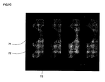
- FIG. 7C illustrates that defects occur in the pixel when the taper reducing layer is not employed in the conventional bottom-emitting OLED.
- FIG. 8 illustrates a cross-sectional view of a bottom-emitting AMOLED having a pixel defining layer in accordance with an embodiment of the present invention.
- FIG. 9A illustrates that the taper angle is reduced by the taper reducing layer in the AMOLED shown in FIG. 8 .
- FIG. 9B illustrates a pixel that the dark spot is not occurred in the AMOLED shown in FIG. 8 .
- FIG. 9C illustrates a pixel where dark spots occur in an OLED having a conventional pixel defining layer.
- FIG. 10 illustrates a cross-sectional view of a top-emitting AMOLED in accordance with a third embodiment of the present invention.
- FIG. 11 illustrates a cross-sectional view of a top-emitting AMOLED having a pixel defining layer in accordance with a fourth embodiment of the present invention.
- FIG. 12 illustrates a cross-sectional view of an AMOLED in accordance with an embodiment of the present invention.
- FIG. 4 illustrates a cross-sectional view of an OLED having a taper angle reduced by a taper reducing layer of the present invention.
- an insulating substrate 40 has a lower layer 41 having an opening 42 for exposing a portion of the insulating substrate 40 .
- the lower layer 41 has a predetermined taper angle with respect to an upper surface of the substrate at an edge of the opening 42 .
- the lower layer 41 has a predetermined step d 0 with respect to the upper surface of the substrate.
- a taper reducing layer 43 having a taper angle ⁇ 2 is formed on the lower layer 41 and the opening 42 .
- the deposition thickness of the taper reducing layer 43 may depend on the step of the substrate surface where the taper reducing layer is deposited. In other words, the taper reducing layer deposited on a portion where the substrate surface has a high step is deposited thinner than the taper reducing layer deposited on a portion where the substrate surface has a low step.
- the taper reducing layer 43 has a thickness of d 2 on the lower layer having the step d 0 , and has a thickness of d 3 , thicker than d 2 on the opening 42 , for exposing the substrate.
- the taper reducing layer 43 Since the thickness of the taper reducing layer 43 depends on the step of the substrate surface, the taper reducing layer 43 has a taper angle smaller than the taper angle at the lower layer 41 . As a result, the taper reducing layer 43 has a taper angle ⁇ 2 smaller than the taper and ⁇ 1 of the lower layer 41 .
- the opening 42 is a contact hole and exposes some portions of the source and drain regions.
- the taper angle of the lower layer 41 becomes ⁇ 1
- the step formed by the contact hole in the insulating layer, with respect to the substrate surface, is d 0 .
- the opening 42 is a via hole and exposes a portion of the source and drain regions.
- the taper angle of the via hole becomes ⁇ 1
- the step formed by the via hole in the passivation layer with respect to the substrate surface is d 0 .
- the opening 42 exposes a portion of a pixel electrode.
- the taper angle of the pixel defining layer at the edge of the opening becomes ⁇ 1
- the step formed by the opening in the pixel defining layer with respect to the substrate surface is d 0 .
- a conductive layer is formed over and below the taper reducing layer 43 , so that the taper reducing layer 43 is formed, for example, of a conductive material.
- An organic layer that has a charge transporting capability and may be coated by a wet coating method may be used for the taper reducing layer 43 .
- the taper reducing layer 43 may consist of at least one organic layer selected from a polymer organic layer, a small-molecule organic layer or similar material.
- the small-molecule organic layer for the taper reducing layer may be selected from carbazole-based, arylamine-based, hydrazone-based, stilbene-based, oxadiazole-based and starburst-based derivatives, and the polymer organic layer is selected from PEDOT, PANI, carbazole-based, arylamine-based, perylene-based, pyrrole-based and oxadiazole-based derivatives or similar materials.
- the lower layer 41 has an opening 42 , such as the contact hole, via hole, or opening region of the pixel defining layer, a step of d 0 and a taper angle of ⁇ 1 with respect to the substrate surface, and a linear slope of tan ⁇ 1 .
- the taper reducing layer 43 has a thickness of d 2 on the lower layer 41 and d 3 on the opening 42 , a taper angle of ⁇ 2 , and a linear slope of tan ⁇ 2 with respect to the substrate surface.
- the minimum thickness of the taper reducing layer required to planarize the substrate surface i.e., the minimum thickness of the taper reducing layer 43 required to have its taper angle ⁇ 2 of zero degree with respect to the substrate surface, is d 1 .
- the taper angle planarized by the taper reducing layer 43 becomes ⁇ 2 , which is the taper angle of the taper reducing layer 43 in the opening 42 .
- the taper angle before it is planarized is ⁇ 1 , which is the taper angle of the lower layer 41 in the opening 42 .
- a point where the substrate surface and the straight line L 1 meet i.e., an edge portion of the opening 42 , is an origin O, where a longitudinal direction of the substrate is an x axis, and a height direction of the substrate is a y axis.
- L1:y1 tan ⁇ 1x
- L 2: y 2 tan ⁇ 2+ d 3 (1)
- the straight line L 1 passes the d 0 at the position x 0 of the x axis direction
- the straight line L 2 passes the d 0 +d 2 at a position x 0 of the x axis direction
- the lines L 1 and L 2 pass d 1 at the position x 1 of the x axis direction.
- d 0 +d 2 may be expressed as the equation 2 below.
- d 0+ d 2 (tan ⁇ 2/tan ⁇ 1) d 0+ d 3 (2)
- a relationship equation with respect to the taper angle ⁇ 2 of the taper reducing layer 43 is obtained from the equation 4 below.
- Thickness d 2 and thickness d 3 of the taper reducing layer 43 to be deposited on the lower layer 41 and the opening 42 , respectively, are obtained from equations 5 and 6 below.
- the thickness d 2 of a portion of the taper reducing layer 43 formed on the lower layer 41 may linearly increase until the thickness d 1 ⁇ d 0 , that is, the thickness when the substrate surface is planarized from the surface of the lower layer 41 .
- the thickness d 3 of a portion where the taper reducing layer 43 is formed in the opening 42 may linearly increase until the thickness d 1 , namely, the thickness when the substrate surface is planarized from the surface of the opening 42 .
- the minimum thickness d 1 required to planarize the substrate surface may vary in accordance with the planarizing capability of the organic layer used for the taper reducing layer, and may be varied and experimentally obtained in accordance with viscosity and volatility of a solution, variables of a coating process, and the like.
- tan ⁇ 2 (1 ⁇ d 2/( d 1 ⁇ d 0))tan ⁇ 1 (4)
- ⁇ is a rate of a planarizing degree for the substrate surface when the taper reducing layer is formed on the substrate with respect to the planarizing degree of the substrate surface when the lower layer by itself is formed on the substrate.
- the lower layer 41 is an insulating layer having a via hole as the opening 42 and has a thickness of 6000 ⁇ and a taper angle ⁇ 1 of 75° in the via hole.
- the minimum thickness d 1 is experimentally assumed to be 8000 ⁇ to entirely planarize the via hole
- the angle ⁇ 2 with which the substrate surface is planarized by the taper reducing layer 43 and the thickness d 3 of the taper reducing layer 43 in the via hole are calculated as described below from the equations 4 and 6 above, to have the taper reducing layer 43 with 1000 ⁇ in thickness to be deposited on the lower layer 41 .
- the thickness d 3 of the taper reducing layer 43 formed in the via hole becomes 4000 ⁇ .
- the taper reducing layer 43 in the via hole is formed to have the taper angle ⁇ 2 of 40°, it may be arithmetically seen that the taper reducing layer 43 is formed with 1540 ⁇ on the lower layer 41 and with 6160 ⁇ in the via hole.
- FIG. 5A shows the number of defects in accordance with the taper angle of the via hole or contact hole.
- the initial defect may include a defect such as a dark pixel that occurred before driving the OLED.
- the thickness d 2 of a portion where the taper reducing layer 43 is formed on the lower layer 41 becomes 1000 ⁇ and the thickness d 3 of a portion where the taper reducing layer 43 is formed in the opening becomes 4000 ⁇ , from the equations 5 and 6,
- FIG. 5B shows a relationship between the taper angle ⁇ 2 and the thickness d 3 of the taper reducing layer formed in the opening when the lower layer 41 formed on the substrate has a predetermined taper angle ⁇ 1 and a step d 1 .
- the taper angle ⁇ 2 of the opening should be 40° or less when a pixel defining layer exists, and the taper angle ⁇ 2 of the contact hole or via hole should be is 60° or less when a pixel defining layer does not exist, in order to fabricate a reliable element.
- a high increase in driving voltage should be avoided when the taper reducing layer 43 is formed with a thickness d 2 of about 1000 ⁇ to about 2000 ⁇ on the lower layer 41 .
- the taper reducing layer used in an exemplary embodiment of the present invention preferably has a planarizing characteristic, a charge transporting capability for transporting a hole or an electron, and a proper HOMO (highest occupied molecular orbital) and LUMO (lowest unfilled molecular orbital), so that it does not increase the driving voltage of the element due to an increased deposition thickness of the taper reducing layer.
- an organic layer having a hole transporting capability may be used, with an HOMO of 4.5 eV or more, and charge mobility of 10 ⁇ 8 cm 2 /Vs or more for the taper reducing layer.
- an organic layer having an electron transporting capability may be used, with an LUMO of 3.5 eV or less, and charge mobility of 10 ⁇ 8 cm 2 /Vs or more for the taper reducing layer.
- the taper reducing layer is employed to an insulating layer having an opening to reduce a taper angle.
- the taper angle may be reduced by the taper reducing layer even in a stepped portion of the deposition layer, so that element defects may be prevented.
- FIG. 6A shows a cross-sectional view of a bottom-emitting OLED having a taper reducing layer in accordance with an embodiment of the present invention.
- a buffer layer 405 is formed on an insulating substrate 400 , and a semiconductor layer 410 , having source and drain regions 411 and 415 , is formed on the buffer layer 405 .
- a gate 425 is formed on a gate insulating layer 420 , and source and drain regions 441 and 445 are connected to the source and drain regions 411 and 415 through contact holes 431 and 435 on an inter-layer insulating layer 430 .
- Wiring 447 such as a data line or a power supply line, is formed at the same time the source and drain electrodes 441 and 445 are formed on the inter-layer insulating layer 430 .
- the contact holes 431 and 435 have a taper angle of 75° and a depth of 5000 ⁇ .
- An anode electrode 470 as a lower electrode connected to one of the source and drain electrodes 441 and 445 , for example, to the drain electrode 445 through the via hole 455 , is formed on a passivation layer 450 .
- the via hole 455 may have a taper angle of 85° and a depth of 5000 ⁇ , and the anode electrode 470 may have a thickness of 1000 ⁇ .
- a cleaning process is performed.
- a taper reducing layer 480 , an organic film layer 485 and a cathode electrode 490 may be sequentially formed on the substrate.
- FIG. 6B illustrates a cross-sectional view of an emission region of an R pixel in an OLED in accordance with an embodiment of the present invention.
- the taper reducing layer 480 is formed on the anode electrode 470
- an emission layer 485 c is formed on the taper reducing layer 480 .
- a polymer organic layer having a hole transporting capability such as, for example, PEDOT is formed with a thickness of 1000 ⁇ on the anode electrode 470 by a spin coating method, and an annealing process is performed by using a hot plate for 5 minutes at 200 ⁇ , thereby forming the taper reducing layer 480 .
- the deposition thickness of the taper reducing layer 480 is determined by its taper angle, the depths and taper angles of the contact hole and via hole below the taper reducing layer, the thickness of the pixel electrode and a taper angle at an edge of the pixel electrode.
- a 600 ⁇ thick CuPc as the hole injecting layer 485 a
- a 300 ⁇ thick NPB as the hole transporting layer 485 b
- a 200 ⁇ thick Alq+DCM as the red color emission layer 485 c
- a 200 ⁇ thick Alq 3 as the electron transporting layer 485 d
- a hole blocking layer between the red color emission layer 485 c and the electron transporting layer 485 d , and an electron injecting layer on the electron transporting layer 485 d may be formed.
- LiF/Al, as the cathode electrode 490 is deposited by a thermal evaporation method.
- a sealant (not shown in the figures) is applied on the insulating substrate 400 to prevent external oxygen and moisture from being introduced inside.
- An encapsulating substrate is bonded thereon, thereby fabricating the OLED.
- FIG. 6C illustrates another cross-sectional view of the emission region of the R pixel in the OLED in accordance with an embodiment of the present invention.
- the taper reducing layer 480 is formed between the emission layer 485 c and the hole transporting layer 485 b of the organic film layer 485 .
- the anode electrode 470 is formed on the insulating layer 400 , and the hole injecting layer 485 a and the hole transporting layer 485 b of the organic film layer 485 are sequentially formed on the anode electrode 470 .
- the taper reducing layer 480 is formed on the hole transporting layer 485 b , the R emission layer 485 c and the electron transporting layer 485 d , as the organic emission layer 485 are sequentially formed on the taper reducing layer 480 .
- the cathode electrode 490 is formed on the electron transporting layer 485 d.
- the taper reducing layer 480 may be formed just on the anode electrode 470 and below the emission layer 485 c , as shown in FIGS. 6B and 6C , and at the same time, may be formed only between the anode electrode 470 and the emission layer 485 c of the organic film layer 485 .
- the organic film layer 485 has at least one of a hole injecting layer, a hole transporting layer, an emission layer, a hole blocking layer, an electron transporting layer and/or an electron injecting layer.
- the contact hole 431 and the via hole 455 have taper angles ( ⁇ 41 , ⁇ 42 ) of 75° and 85° , respectively, before forming the taper reducing layer 480 .
- the taper angle is reduced with respect to the substrate 400 surface after the taper reducing layer 480 is formed, so that the taper angles ( ⁇ 43 , ⁇ 44 ) of the contact hole 431 and the via hole 455 are 60° or less.
- the anode electrode 470 has an edge taper angle and the taper reducing layer 480 may reduce it to an edge taper angle ( ⁇ 45 ) of 40°.
- the taper angle ( ⁇ 46 ) may be reduced near the contact holes 431 and 435 , near the via hole 455 , and near the wiring 447 in accordance with formation of the taper reducing layer 480 .
- the deposition thickness of the taper reducing layer 480 is determined by the taper angle of the taper reducing layer, the depths and taper angles of the contact hole and via hole below the taper reducing layer, the thickness of the pixel electrode and the taper angle at an edge of the pixel electrode.
- the taper reducing layer is deposited to have the taper angles of the contact hole or via hole of 60° or less, from FIG.
- the deposition thickness of the taper reducing layer is determined by the taper angle of the contact hole and the thickness of the insulating layer, such as the inter-layer insulating layer and the gate insulating layer where the contact hole is formed, and further determined by the taper angle of the via hole and the thickness of the insulating layer, such as the passivation layer where the via hole is formed.
- the deposition thickness of the taper reducing layer is determined by the taper angle at an edge of the pixel electrode and the thickness of the pixel electrode, from FIG. 4 a and equations 4 to 6.
- FIG. 7A illustrates a SEM picture near the via hole in the OLED in accordance with a first exemplary embodiment of the present invention.
- a portion with a thickness d 73 where the taper reducing layer is formed on the anode electrode within the via hole is deposited thicker than a portion with a thickness d 72 where the taper reducing layer is formed on the anode electrode over an insulating layer having a stepped portion, so that the taper angle in the via hole is reduced to 50°.
- FIG. 7B illustrates a microscope picture for representing whether edge defects occur in the emission region when the OLED of the first exemplary embodiment is driven. Referring to FIG.
- FIG. 7C illustrates a microscope picture for representing whether the edge defects occur at an edge of the emission region when the OLED having the same structure as shown in FIGS. 1A and 1B is driven. Referring to FIG. 7C , it may be seen that dark spots may occur at an edge of the emission region when the taper reducing layer is not used.
- a numerical reference 71 indicates the dark spot near the via hole
- 72 indicates the dark spot near the contact hole.
- FIG. 8 illustrates a cross-sectional view of a bottom-emitting OLED in accordance with a second exemplary embodiment of the present invention.
- a buffer layer 505 is formed on an insulating substrate 500
- a semiconductor layer 510 having source and drain regions 511 and 515 is formed on the buffer layer 505 .
- a gate 525 is formed on a gate insulating layer 520
- source and drain electrodes 541 and 545 are formed on an inter-layer insulating layer 530 through contact holes 531 and 535 .
- a data line 547 is formed at the same time when the source and drain electrodes 541 and 545 are formed on the inter-layer insulating layer 530 .
- this pixel defining layer is etched to have a taper angle ⁇ 51 of 60° to form an opening 575 .
- the taper reducing layer 580 may have a taper angle ⁇ 51 of the opening 575 of 40° or less, and the deposition thickness of the taper reducing layer 580 is determined by the taper angle of the taper reducing layer 580 , thickness of the pixel defining layer 585 and the taper angle of the opening 575 .
- an encapsulating substrate (not shown) is then bonded to fabricate the OLED in accordance with second exemplary embodiment of the present invention.
- FIG. 9A illustrates a SEM picture near an emission region of an OLED in accordance with a second exemplary embodiment. Referring to FIG. 9A , it may be seen that the taper angle at an edge of the opening is reduced to 40° as the taper reducing layer is formed.
- FIG. 9B illustrates a microscope picture of an edge of the emission region when the OLED employing the taper reducing layer in accordance with the second exemplary embodiment is driven.
- defects such as a dark spot at an edge of the emission region
- FIG. 9C illustrates a microscope picture at an edge of the emission region when the OLED, having the pixel defining layer and employing a conventional taper reducing layer, is driven.
- dark spots occur if the taper angle at an edge of the opening is large even when the pixel defining layer is used.
- FIG. 10 illustrates a cross-sectional view of a top-emitting OLED in accordance with a third exemplary embodiment of the present invention.
- a buffer layer 605 is formed on an insulating layer 600
- a semiconductor layer 610 having source and drain regions 611 and 615 is formed on the buffer layer 605 .
- a gate 625 is formed on a gate insulating layer 620
- source and drain electrodes 641 and 645 are formed on an inter-layer insulating layer 630 through contact holes 631 and 635 .
- wiring 647 such as a data line or a power supply line, is formed when the source and drain electrodes 641 and 645 are formed on the inter-layer insulating layer 630 .
- a planarization layer 660 is formed on a passivation layer 650 , and an anode electrode 670 as a lower electrode connected to one of the source and drain electrodes 641 and 645 , such as, for example, to the drain electrode 645 through the via hole 655 , is formed on the planarization layer 660 .
- PEDOT as an organic layer that may be coated by a wet coating method and has a hole transporting capability is deposited on the substrate, may be used so that the taper reducing layer 680 is formed.
- the taper reducing layer 680 may have the taper angle of the via hole of 60° or less, and the deposition thickness of the taper reducing layer 680 is determined by the taper angle of the taper reducing layer, thickness of the planarization layer 660 and the taper angle of the via hole.
- an encapsulating substrate (not shown in the figure) is then used to fabricate the OLED in accordance with the third exemplary embodiment.
- FIG. 11 illustrates a cross-sectional view of a top-emitting OLED in accordance with a fourth exemplary embodiment of the invention.
- a buffer layer 705 is formed on an insulating substrate 700 , and a semiconductor layer 710 having source and drain regions 711 and 715 is formed on the buffer layer 705 .
- a gate 725 is formed on a gate insulating layer 720 , and source and drain electrodes 741 and 745 are formed on an inter-layer insulating layer 730 through contact holes 731 and 735 .
- wiring 747 such as a data line or a power supply line, is formed when the source and drain electrodes 741 and 745 are formed on the inter-layer insulating layer 730 .
- a planarization layer 760 is formed on a passivation layer 750 , and an anode electrode 770 as a lower electrode connected to one of the source and drain electrodes 741 and 745 , such as, for example, to the drain electrode 745 through the via hole 755 , is formed on the planarization layer 760 .
- a pixel defining layer 765 having an opening 775 for exposing a portion of the anode electrode 770 , is then formed.
- PEDOT as an organic layer that may be coated by a wet coating method and has a hole transporting capability, may be deposited on the substrate, so that the taper reducing layer 780 is formed.
- taper reducing layer 780 may have the taper angle of the opening 775 of 40° or less, and the deposition thickness of the taper reducing layer 780 is determined by the taper angle of the taper reducing layer, the thickness of the pixel defining layer and the taper angle of the pixel defining layer.
- an encapsulating substrate (not shown in the figure) is used to fabricate the OLED in accordance with the fourth exemplary embodiment.
- FIG. 12 illustrates a cross-sectional view of a bottom-emitting OLED in accordance with a fifth exemplary embodiment of the present invention.
- a buffer layer 805 is formed on an insulating substrate 800 , and a semiconductor layer 810 having source and drain regions 811 and 815 is formed on the buffer layer 805 .
- a gate 825 is formed on a gate insulating layer 820 , and source and drain electrodes 841 and 845 are formed through contact holes 831 and 835 on an inter-layer insulating layer 830 .
- an anode electrode 870 is formed to be connected to one of the source and drain electrodes 841 and 845 , such as, for example, to the drain electrode 845 on the inter-layer insulating layer 830 .
- a passivation layer 850 having an opening 855 for exposing a portion of the anode electrode 870 is formed on the substrate.
- the taper reducing layer 880 may have a taper angle in the opening of 40° or less, and the thickness of the taper reducing layer 880 is determined by the taper angle of the taper reducing layer 880 , the thickness of the passivation layer 850 and the taper angle of the opening.
- an encapsulating substrate (not shown in the figure) is bonded to fabricate the OLED in accordance with the fifth exemplary embodiment.
- the organic film layer has the hole injecting layer, the hole transporting layer, the R, G, or B organic emission layer and the electron transporting layer. However, it may have at least one of the hole injecting layer, the hole transporting layer, the R, G, or B organic emission layer, the hole blocking layer, the electron transporting layer and/or the electron injecting layer.
- top and bottom-emitting OLEDs where the organic emission layer is deposited on the anode electrode, use the organic layer having a hole transporting capability for the taper reducing layer.
- the organic layer having the electron transporting capability for the taper reducing layer in the inverted-type OLED where the organic emission layer is deposited on the cathode electrode.
- the taper reducing layer is shown to be formed between the anode electrode and the organic film layer in the exemplary embodiments of the present invention. However, it is possible to form the taper reducing layer on any layer existing between the emission layer of the organic film layer and the anode electrode in the top and bottom-emitting OLEDs. It is also possible to form it on any layer existing between the emission layer of the organic film layer and the cathode electrode in the inverted-type OLED.
- the method for reducing the taper angle of the substrate surface by using the taper reducing layer of the present invention may use various methods, such as, for example, but not limited to, a deposition method, an inkjet method and a laser-induced thermal imaging for forming the organic emission layer.
- the organic film layer capable of reducing the taper angle between the organic emission layer and the lower electrode in accordance with the exemplary embodiments of the present invention, defects near the contact hole and via hole and at a stepped portion of the lower electrode and defects of the organic emission layer may be prevented, and reliability and the yield may also be improved.
Abstract
Description
tan θ2=(1−d2/(d1−d0))tan θ1
d2=(d1−d0)(1−tan θ2/tan θ1)
d3=d1(1−tan θ2/tan θ1),
-
- wherein d1 is a deposition thickness of the upper layer when the second taper angle of the upper layer becomes 0°.
L1:y1=tan θ1x
L2:y2=tan θ2+d3 (1)
L1:d0=tan θ1x0
L2:d0+d2=tan θ2x0+d3
d0+d2=(tan θ2/tan θ1)d0+d3 (2)
L1:d1=tan θ1x1
L2:d1=tan θ2x1+d3
d1=(tan θ2/tan θ1)d1+d3 (3)
tan θ2=(1−d2/(d1−d0))tan θ1 (4)
d2=(d1−d0)(1−tan θ2/tan θ1)=(d1−d0)(1−α) (5)
d3=d1(1−tan θ2/tan θ1)=d1(1−α) (6)
tan θ2=(1−1000/2000)tan 75=0.5*3.73=1.87
θ2=tan−1(1.87)=62°.
d3=d1(1−tan θ2/tan θ1)=d1*d2/(d1−d0)=8000*1000/2000=4000
d2=2000(1−tan 40/tan 75)=2000(1−0.23)=1540
d3=8000(1−tan 40/tan 75)=8000(1−0.23)=6160
Claims (6)
Applications Claiming Priority (3)
| Application Number | Priority Date | Filing Date | Title |
|---|---|---|---|
| KR1020030084746A KR100741962B1 (en) | 2003-11-26 | 2003-11-26 | Flat Panel Display |
| KR2003-84746 | 2003-11-26 | ||
| KR10-2003-0084746 | 2003-11-26 |
Publications (2)
| Publication Number | Publication Date |
|---|---|
| US20050116240A1 US20050116240A1 (en) | 2005-06-02 |
| US8063550B2 true US8063550B2 (en) | 2011-11-22 |
Family
ID=34464754
Family Applications (1)
| Application Number | Title | Priority Date | Filing Date |
|---|---|---|---|
| US10/947,421 Active 2027-04-07 US8063550B2 (en) | 2003-11-26 | 2004-09-23 | Flat panel display with taper reducing layer |
Country Status (5)
| Country | Link |
|---|---|
| US (1) | US8063550B2 (en) |
| EP (1) | EP1536471B1 (en) |
| JP (1) | JP2005158672A (en) |
| KR (1) | KR100741962B1 (en) |
| CN (2) | CN101257038B (en) |
Cited By (4)
| Publication number | Priority date | Publication date | Assignee | Title |
|---|---|---|---|---|
| US8729535B2 (en) | 2010-05-07 | 2014-05-20 | Panasonic Corporation | Organic EL display panel and method for producing same |
| US8957421B2 (en) | 2012-08-20 | 2015-02-17 | Samsung Display Co., Ltd. | Flat panel display and method of manufacturing the same |
| US9711602B2 (en) * | 2015-06-25 | 2017-07-18 | Boe Technology Group Co., Ltd. | Method of making thin film transistor array and source/drain contact via-interconnect structures formed thereby |
| US9960217B2 (en) | 2009-04-13 | 2018-05-01 | Innolux Corporation | Display panel and system for displaying images utilizing the same |
Families Citing this family (50)
| Publication number | Priority date | Publication date | Assignee | Title |
|---|---|---|---|---|
| KR100611159B1 (en) * | 2003-11-29 | 2006-08-09 | 삼성에스디아이 주식회사 | Oled |
| KR100683695B1 (en) * | 2004-11-11 | 2007-02-15 | 삼성에스디아이 주식회사 | Organic light emitting device |
| US7259405B2 (en) * | 2004-11-23 | 2007-08-21 | Au Optronics Corporation | Organic photoelectric device with improved electron transport efficiency |
| KR102381391B1 (en) * | 2015-04-16 | 2022-03-31 | 삼성디스플레이 주식회사 | Display device |
| US8016629B2 (en) * | 2005-04-25 | 2011-09-13 | Showa Denko K.K. | Method of producing a display device |
| US7795592B2 (en) * | 2005-11-21 | 2010-09-14 | Fujifilm Corporation | Image detector and manufacturing method of the same |
| JP5235269B2 (en) * | 2005-12-19 | 2013-07-10 | エルジー ディスプレイ カンパニー リミテッド | Image display device and manufacturing method thereof |
| KR100673765B1 (en) | 2006-01-20 | 2007-01-24 | 삼성에스디아이 주식회사 | Organic light-emitting display device and the preparing method of the same |
| US8038495B2 (en) | 2006-01-20 | 2011-10-18 | Samsung Mobile Display Co., Ltd. | Organic light-emitting display device and manufacturing method of the same |
| KR100635514B1 (en) | 2006-01-23 | 2006-10-18 | 삼성에스디아이 주식회사 | Organic electroluminescence display device and method for fabricating of the same |
| KR100688795B1 (en) | 2006-01-25 | 2007-03-02 | 삼성에스디아이 주식회사 | Organic light-emitting display device and the preparing method of the same |
| KR100685853B1 (en) | 2006-01-25 | 2007-02-22 | 삼성에스디아이 주식회사 | Organic electroluminescence device and method for fabricating of the same |
| KR100685854B1 (en) * | 2006-01-25 | 2007-02-22 | 삼성에스디아이 주식회사 | Organic electroluminescence device and method for fabricating of the same |
| US8164257B2 (en) | 2006-01-25 | 2012-04-24 | Samsung Mobile Display Co., Ltd. | Organic light emitting display and method of fabricating the same |
| KR100671641B1 (en) | 2006-01-25 | 2007-01-19 | 삼성에스디아이 주식회사 | Organic light emitting display device and fabricating method the same |
| KR100671647B1 (en) | 2006-01-26 | 2007-01-19 | 삼성에스디아이 주식회사 | Organic light emitting display device |
| JP4633674B2 (en) | 2006-01-26 | 2011-02-16 | 三星モバイルディスプレイ株式會社 | Organic electroluminescent display device and manufacturing method thereof |
| KR100671639B1 (en) | 2006-01-27 | 2007-01-19 | 삼성에스디아이 주식회사 | Organic light emitting display device and fabricating method of the same |
| KR100688790B1 (en) | 2006-01-27 | 2007-03-02 | 삼성에스디아이 주식회사 | Organic light emitting display device and fabricating method of the same |
| KR100732817B1 (en) | 2006-03-29 | 2007-06-27 | 삼성에스디아이 주식회사 | Organic light-emitting display device and the preparing method of the same |
| KR100736577B1 (en) * | 2006-04-07 | 2007-07-06 | 엘지전자 주식회사 | Light emitting diode and method for manufacturing the same |
| TWI358964B (en) * | 2006-04-12 | 2012-02-21 | Au Optronics Corp | Electroluminescence display element and method for |
| JP2008147418A (en) * | 2006-12-11 | 2008-06-26 | Hitachi Ltd | Thin film transistor device, image display device, and method of manufacturing same |
| KR100870363B1 (en) | 2007-03-15 | 2008-11-25 | 삼성에스디아이 주식회사 | Protection circuit board for secondary battery and secondary battery using the same |
| KR100900444B1 (en) * | 2007-06-27 | 2009-06-02 | 엘지전자 주식회사 | Organic Light Emitting Diode Display Device And Manufacturing Of The Same |
| JP5489542B2 (en) * | 2008-07-01 | 2014-05-14 | キヤノン株式会社 | Radiation detection apparatus and radiation imaging system |
| WO2010038181A1 (en) * | 2008-10-02 | 2010-04-08 | Philips Intellectual Property & Standards Gmbh | Oled device with covered shunt line |
| US8101699B2 (en) * | 2008-12-02 | 2012-01-24 | General Electric Company | Electron-transporting polymers |
| US8921726B2 (en) | 2009-02-06 | 2014-12-30 | Lg Chem, Ltd. | Touch screen and manufacturing method thereof |
| KR20100090628A (en) | 2009-02-06 | 2010-08-16 | 주식회사 엘지화학 | Preparation method for insulated conductive pattern |
| CN102308367B (en) * | 2009-02-06 | 2015-06-10 | Lg化学株式会社 | Method for manufacturing insulated conductive pattern and laminate |
| JP2010245366A (en) * | 2009-04-08 | 2010-10-28 | Fujifilm Corp | Electronic device, method of manufacturing the same, and display device |
| US20100270537A1 (en) * | 2009-04-22 | 2010-10-28 | General Electric Company | Optoelectronic devices and organic compounds used therein |
| CN101872780B (en) * | 2009-04-23 | 2013-11-27 | 群创光电股份有限公司 | Display panel and image display system using same |
| CN103606549B (en) * | 2009-04-23 | 2017-06-09 | 群创光电股份有限公司 | Display panel and the image display system using the display panel |
| CN102598891B (en) | 2009-07-16 | 2015-11-25 | Lg化学株式会社 | Electric conductor and manufacture method thereof |
| KR101084193B1 (en) * | 2010-02-16 | 2011-11-17 | 삼성모바일디스플레이주식회사 | An organic light emitting display device and the manufacturing method thereof |
| JP5519537B2 (en) * | 2010-05-07 | 2014-06-11 | パナソニック株式会社 | Organic EL display panel and manufacturing method thereof |
| JP5677890B2 (en) * | 2010-09-30 | 2015-02-25 | 富士フイルム株式会社 | Photoelectric conversion element, method for manufacturing photoelectric conversion element, and imaging element |
| US20150155516A1 (en) * | 2012-06-20 | 2015-06-04 | Panasonic Corporation | Organic light-emitting element and production method therefor |
| JP5418862B2 (en) * | 2012-09-10 | 2014-02-19 | ソニー株式会社 | Display device |
| KR20140046331A (en) * | 2012-10-10 | 2014-04-18 | 삼성디스플레이 주식회사 | Organic light emitting display apparatus and method of manufacturing the same |
| JP2014123628A (en) * | 2012-12-20 | 2014-07-03 | Japan Display Inc | Organic electroluminescent display device and method for manufacturing the same |
| CN104425544B (en) * | 2013-09-09 | 2017-07-07 | 瀚宇彩晶股份有限公司 | The dot structure of organic light emitting diode display |
| JP6457879B2 (en) * | 2015-04-22 | 2019-01-23 | 株式会社ジャパンディスプレイ | Display device and manufacturing method thereof |
| KR102379194B1 (en) * | 2015-05-11 | 2022-03-29 | 삼성디스플레이 주식회사 | Organic light emitting display panel and fabrication method thereof |
| US20180314099A1 (en) * | 2015-11-06 | 2018-11-01 | Sharp Kabushiki Kaisha | Display board, display device, and method of producing display board |
| CN108231673B (en) * | 2018-01-19 | 2020-07-03 | 京东方科技集团股份有限公司 | Display panel, manufacturing method thereof and display device |
| CN108400152B (en) * | 2018-03-30 | 2022-06-10 | 京东方科技集团股份有限公司 | Manufacturing method of OLED display screen and OLED display screen |
| CN114460772A (en) * | 2022-01-26 | 2022-05-10 | 武汉华星光电技术有限公司 | Array substrate and display panel |
Citations (30)
| Publication number | Priority date | Publication date | Assignee | Title |
|---|---|---|---|---|
| KR950010703A (en) | 1993-09-23 | 1995-04-28 | 박경팔 | Field emission emitter and method of manufacturing the same |
| JPH08227276A (en) | 1995-02-21 | 1996-09-03 | Pioneer Electron Corp | Organic electroluminescence display panel and its production |
| US5684365A (en) | 1994-12-14 | 1997-11-04 | Eastman Kodak Company | TFT-el display panel using organic electroluminescent media |
| EP1058311A2 (en) | 1999-06-04 | 2000-12-06 | Semiconductor Energy Laboratory Co., Ltd. | Electro-optical device and electronic device |
| EP1063704A2 (en) | 1999-06-21 | 2000-12-27 | Semiconductor Energy Laboratory Co., Ltd. | EL display device, driving method thereof, and electronic equipment provided with the EL display device |
| KR20010003764A (en) | 1999-06-25 | 2001-01-15 | 김영환 | Method of manufacturing organic field emission display device |
| US6246179B1 (en) | 1998-12-01 | 2001-06-12 | Sanyo Electric Co., Ltd. | Emissive element and display device using such element |
| US6252297B1 (en) * | 1997-03-07 | 2001-06-26 | Kabushiki Kaisha Toshiba | Array substrate, liquid crystal display device and their manufacturing method |
| JP2001189192A (en) | 1999-10-12 | 2001-07-10 | Semiconductor Energy Lab Co Ltd | Light emission device and manufacturing method of the same |
| JP2001195016A (en) | 1999-10-29 | 2001-07-19 | Semiconductor Energy Lab Co Ltd | Electronic device |
| US6274887B1 (en) * | 1998-11-02 | 2001-08-14 | Semiconductor Energy Laboratory Co., Ltd. | Semiconductor device and manufacturing method therefor |
| JP2001312223A (en) | 2000-02-22 | 2001-11-09 | Semiconductor Energy Lab Co Ltd | Spontaneous light emitting device and method for manufacturing the same |
| JP2002164181A (en) | 2000-09-18 | 2002-06-07 | Semiconductor Energy Lab Co Ltd | Display device and its manufacturing method |
| JP2002175029A (en) | 2000-09-29 | 2002-06-21 | Sanyo Electric Co Ltd | Semiconductor device and display device |
| JP2002208491A (en) | 2000-11-09 | 2002-07-26 | Toshiba Corp | Self-illuminating display device |
| US20020113248A1 (en) | 2001-02-19 | 2002-08-22 | Semiconductor Energy Laboratory Co., Ltd. | Light emitting device and method of manufacturing the same |
| US20020140643A1 (en) * | 2001-03-28 | 2002-10-03 | Toshihiro Sato | Display module |
| JP2003022892A (en) | 2001-07-06 | 2003-01-24 | Semiconductor Energy Lab Co Ltd | Manufacturing method of light emitting device |
| JP2003091246A (en) | 2001-09-18 | 2003-03-28 | Matsushita Electric Ind Co Ltd | Organic electro-luminescence display panel and manufacturing method therefor |
| JP2003131593A (en) | 2001-10-26 | 2003-05-09 | Sharp Corp | Active matrix driven organic led panel |
| EP1315209A2 (en) | 2001-11-26 | 2003-05-28 | Samsung SDI Co. Ltd. | Organic EL display device and method of manufacturing the same |
| US6573651B2 (en) * | 2000-12-18 | 2003-06-03 | The Trustees Of Princeton University | Highly efficient OLEDs using doped ambipolar conductive molecular organic thin films |
| EP1331667A2 (en) | 2002-01-25 | 2003-07-30 | Semiconductor Energy Laboratory Co., Ltd. | A display device and method for manufacturing thereof |
| US20030146695A1 (en) | 2001-12-18 | 2003-08-07 | Seiko Epson Corporation | Display apparatus and electric device |
| JP2003243171A (en) | 2002-02-18 | 2003-08-29 | Matsushita Electric Ind Co Ltd | Organic electroluminescent display panel and its manufacturing method |
| US20030170491A1 (en) * | 2002-02-15 | 2003-09-11 | Eastman Kodak Company | Providing an organic electroluminescent device having stacked electroluminescent units |
| JP2003313655A (en) | 2002-02-25 | 2003-11-06 | Semiconductor Energy Lab Co Ltd | Producing apparatus |
| JP2004031262A (en) | 2002-06-28 | 2004-01-29 | Matsushita Electric Ind Co Ltd | Organic electroluminescence panel |
| KR20040062023A (en) | 2002-12-31 | 2004-07-07 | 엘지전자 주식회사 | Field emission device and manufacturing method thereof |
| JP2004234901A (en) | 2003-01-28 | 2004-08-19 | Seiko Epson Corp | Display substrate, organic el display device, manufacturing method of display substrate and electronic apparatus |
Family Cites Families (3)
| Publication number | Priority date | Publication date | Assignee | Title |
|---|---|---|---|---|
| JP2001031223A (en) * | 1999-07-21 | 2001-02-06 | Murata Mach Ltd | Rack of automated storage and retrieval system |
| JP2001131593A (en) * | 1999-11-09 | 2001-05-15 | Asahi Kasei Corp | Nonflammable detergent |
| JP4302901B2 (en) * | 2001-02-27 | 2009-07-29 | 三星モバイルディスプレイ株式會社 | Luminescent body and light emitting system |
-
2003
- 2003-11-26 KR KR1020030084746A patent/KR100741962B1/en active IP Right Grant
-
2004
- 2004-03-19 JP JP2004081618A patent/JP2005158672A/en active Pending
- 2004-09-23 US US10/947,421 patent/US8063550B2/en active Active
- 2004-10-18 EP EP04090398.1A patent/EP1536471B1/en active Active
- 2004-11-05 CN CN2008100819968A patent/CN101257038B/en active Active
- 2004-11-05 CN CNB2004100897615A patent/CN100511753C/en active Active
Patent Citations (33)
| Publication number | Priority date | Publication date | Assignee | Title |
|---|---|---|---|---|
| KR950010703A (en) | 1993-09-23 | 1995-04-28 | 박경팔 | Field emission emitter and method of manufacturing the same |
| US5684365A (en) | 1994-12-14 | 1997-11-04 | Eastman Kodak Company | TFT-el display panel using organic electroluminescent media |
| JPH08227276A (en) | 1995-02-21 | 1996-09-03 | Pioneer Electron Corp | Organic electroluminescence display panel and its production |
| US6252297B1 (en) * | 1997-03-07 | 2001-06-26 | Kabushiki Kaisha Toshiba | Array substrate, liquid crystal display device and their manufacturing method |
| US6274887B1 (en) * | 1998-11-02 | 2001-08-14 | Semiconductor Energy Laboratory Co., Ltd. | Semiconductor device and manufacturing method therefor |
| US6246179B1 (en) | 1998-12-01 | 2001-06-12 | Sanyo Electric Co., Ltd. | Emissive element and display device using such element |
| EP1058311A2 (en) | 1999-06-04 | 2000-12-06 | Semiconductor Energy Laboratory Co., Ltd. | Electro-optical device and electronic device |
| EP1063704A2 (en) | 1999-06-21 | 2000-12-27 | Semiconductor Energy Laboratory Co., Ltd. | EL display device, driving method thereof, and electronic equipment provided with the EL display device |
| KR20010003764A (en) | 1999-06-25 | 2001-01-15 | 김영환 | Method of manufacturing organic field emission display device |
| JP2001189192A (en) | 1999-10-12 | 2001-07-10 | Semiconductor Energy Lab Co Ltd | Light emission device and manufacturing method of the same |
| JP2001195016A (en) | 1999-10-29 | 2001-07-19 | Semiconductor Energy Lab Co Ltd | Electronic device |
| JP2001312223A (en) | 2000-02-22 | 2001-11-09 | Semiconductor Energy Lab Co Ltd | Spontaneous light emitting device and method for manufacturing the same |
| JP2002164181A (en) | 2000-09-18 | 2002-06-07 | Semiconductor Energy Lab Co Ltd | Display device and its manufacturing method |
| JP2002175029A (en) | 2000-09-29 | 2002-06-21 | Sanyo Electric Co Ltd | Semiconductor device and display device |
| JP2002208491A (en) | 2000-11-09 | 2002-07-26 | Toshiba Corp | Self-illuminating display device |
| US6573651B2 (en) * | 2000-12-18 | 2003-06-03 | The Trustees Of Princeton University | Highly efficient OLEDs using doped ambipolar conductive molecular organic thin films |
| CN1372325A (en) | 2001-02-19 | 2002-10-02 | 株式会社半导体能源研究所 | Illumination device and making method thereof |
| US20020113248A1 (en) | 2001-02-19 | 2002-08-22 | Semiconductor Energy Laboratory Co., Ltd. | Light emitting device and method of manufacturing the same |
| US20020140643A1 (en) * | 2001-03-28 | 2002-10-03 | Toshihiro Sato | Display module |
| JP2003022892A (en) | 2001-07-06 | 2003-01-24 | Semiconductor Energy Lab Co Ltd | Manufacturing method of light emitting device |
| JP2003091246A (en) | 2001-09-18 | 2003-03-28 | Matsushita Electric Ind Co Ltd | Organic electro-luminescence display panel and manufacturing method therefor |
| JP2003131593A (en) | 2001-10-26 | 2003-05-09 | Sharp Corp | Active matrix driven organic led panel |
| EP1315209A2 (en) | 2001-11-26 | 2003-05-28 | Samsung SDI Co. Ltd. | Organic EL display device and method of manufacturing the same |
| CN1423513A (en) | 2001-11-26 | 2003-06-11 | 三星Sdi株式会社 | Organic electrofluorescent display and manufacturing method thereof |
| US20030146695A1 (en) | 2001-12-18 | 2003-08-07 | Seiko Epson Corporation | Display apparatus and electric device |
| EP1331667A2 (en) | 2002-01-25 | 2003-07-30 | Semiconductor Energy Laboratory Co., Ltd. | A display device and method for manufacturing thereof |
| US20030227253A1 (en) * | 2002-01-25 | 2003-12-11 | Semiconductor Energy Laboratory Co., Ltd. | Display device and method for manufacturing thereof |
| US20030170491A1 (en) * | 2002-02-15 | 2003-09-11 | Eastman Kodak Company | Providing an organic electroluminescent device having stacked electroluminescent units |
| JP2003243171A (en) | 2002-02-18 | 2003-08-29 | Matsushita Electric Ind Co Ltd | Organic electroluminescent display panel and its manufacturing method |
| JP2003313655A (en) | 2002-02-25 | 2003-11-06 | Semiconductor Energy Lab Co Ltd | Producing apparatus |
| JP2004031262A (en) | 2002-06-28 | 2004-01-29 | Matsushita Electric Ind Co Ltd | Organic electroluminescence panel |
| KR20040062023A (en) | 2002-12-31 | 2004-07-07 | 엘지전자 주식회사 | Field emission device and manufacturing method thereof |
| JP2004234901A (en) | 2003-01-28 | 2004-08-19 | Seiko Epson Corp | Display substrate, organic el display device, manufacturing method of display substrate and electronic apparatus |
Non-Patent Citations (2)
| Title |
|---|
| A. Elschner, F. Jonas et al, "High-Resistivity PEDT/PSS for Reduced Crosstalk in Passive Matrix OELs", Asia Display/IDW' 01, 2001, pp. 1427-1430. |
| Yoshihara Sato, "Molecular Electronics and Bioelectronics", Japan Society of Applied Physics, 2000, vol. 11, No. 1, pp. 86-99. |
Cited By (4)
| Publication number | Priority date | Publication date | Assignee | Title |
|---|---|---|---|---|
| US9960217B2 (en) | 2009-04-13 | 2018-05-01 | Innolux Corporation | Display panel and system for displaying images utilizing the same |
| US8729535B2 (en) | 2010-05-07 | 2014-05-20 | Panasonic Corporation | Organic EL display panel and method for producing same |
| US8957421B2 (en) | 2012-08-20 | 2015-02-17 | Samsung Display Co., Ltd. | Flat panel display and method of manufacturing the same |
| US9711602B2 (en) * | 2015-06-25 | 2017-07-18 | Boe Technology Group Co., Ltd. | Method of making thin film transistor array and source/drain contact via-interconnect structures formed thereby |
Also Published As
| Publication number | Publication date |
|---|---|
| JP2005158672A (en) | 2005-06-16 |
| KR20050051058A (en) | 2005-06-01 |
| EP1536471A3 (en) | 2007-08-15 |
| CN1622699A (en) | 2005-06-01 |
| CN101257038B (en) | 2010-07-14 |
| CN101257038A (en) | 2008-09-03 |
| EP1536471A2 (en) | 2005-06-01 |
| EP1536471B1 (en) | 2019-10-02 |
| US20050116240A1 (en) | 2005-06-02 |
| KR100741962B1 (en) | 2007-07-23 |
| CN100511753C (en) | 2009-07-08 |
Similar Documents
| Publication | Publication Date | Title |
|---|---|---|
| US8063550B2 (en) | Flat panel display with taper reducing layer | |
| US7501756B2 (en) | Organic light emitting display | |
| US7936125B2 (en) | Flat panel display | |
| US7456566B2 (en) | Top-emission type organic electroluminescence display device and method for fabricating the same | |
| US7863811B2 (en) | Organic light emitting display apparatus and method of manufacturing the same | |
| US7456811B2 (en) | Organic electro-luminescent display device and method of manufacturing the same | |
| KR100656490B1 (en) | Full Color OLED and Method for fabricating the Same | |
| KR100552872B1 (en) | Organic electroluminescence panel | |
| US7335923B2 (en) | Electroluminescence display device | |
| US8716058B2 (en) | Organic light-emitting display device and method of manufacturing the same | |
| KR101923172B1 (en) | Organic light emitting display apparatus and the method for manufacturing of the same | |
| US7221089B2 (en) | Organic light emitting diode display device and method of manufacturing the same | |
| US20060082292A1 (en) | Organic light emitting display and method of fabricating the same | |
| KR100647599B1 (en) | Organic electro-luminescent display device and fabricating the same | |
| KR101383454B1 (en) | Light emitting device | |
| US9397297B2 (en) | Optical patterning mask and method of fabricating display device using the same | |
| KR20050099027A (en) | Top emission oled using assistant electrode to prevent ir drop and fabricating the same | |
| KR100712212B1 (en) | The method for fabricating of organic electroluminescence device | |
| CN115176300A (en) | Display device and method for manufacturing display device | |
| KR100625969B1 (en) | Electro luminescence device | |
| KR100728790B1 (en) | Organic light emitting display and method of manufacturing the same | |
| KR20050082103A (en) | Active matrix type organic electro luminescence display device and fabrication method of the same |
Legal Events
| Date | Code | Title | Description |
|---|---|---|---|
| AS | Assignment |
Owner name: SAMSUNG SDI CO., LTD., KOREA, REPUBLIC OF Free format text: ASSIGNMENT OF ASSIGNORS INTEREST;ASSIGNORS:KIM, MU-HYUN;CHIN, BYUNG-DOO;SONG, MYUNG-WON;AND OTHERS;REEL/FRAME:015817/0370 Effective date: 20040909 |
|
| AS | Assignment |
Owner name: SAMSUNG MOBILE DISPLAY CO., LTD., KOREA, REPUBLIC Free format text: ASSIGNMENT OF ASSIGNORS INTEREST;ASSIGNOR:SAMSUNG SDI CO., LTD.;REEL/FRAME:022024/0026 Effective date: 20081212 Owner name: SAMSUNG MOBILE DISPLAY CO., LTD.,KOREA, REPUBLIC O Free format text: ASSIGNMENT OF ASSIGNORS INTEREST;ASSIGNOR:SAMSUNG SDI CO., LTD.;REEL/FRAME:022024/0026 Effective date: 20081212 |
|
| FEPP | Fee payment procedure |
Free format text: PAYOR NUMBER ASSIGNED (ORIGINAL EVENT CODE: ASPN); ENTITY STATUS OF PATENT OWNER: LARGE ENTITY |
|
| STCF | Information on status: patent grant |
Free format text: PATENTED CASE |
|
| AS | Assignment |
Owner name: SAMSUNG DISPLAY CO., LTD., KOREA, REPUBLIC OF Free format text: MERGER;ASSIGNOR:SAMSUNG MOBILE DISPLAY CO., LTD.;REEL/FRAME:028884/0453 Effective date: 20120702 |
|
| FPAY | Fee payment |
Year of fee payment: 4 |
|
| MAFP | Maintenance fee payment |
Free format text: PAYMENT OF MAINTENANCE FEE, 8TH YEAR, LARGE ENTITY (ORIGINAL EVENT CODE: M1552); ENTITY STATUS OF PATENT OWNER: LARGE ENTITY Year of fee payment: 8 |
|
| MAFP | Maintenance fee payment |
Free format text: PAYMENT OF MAINTENANCE FEE, 12TH YEAR, LARGE ENTITY (ORIGINAL EVENT CODE: M1553); ENTITY STATUS OF PATENT OWNER: LARGE ENTITY Year of fee payment: 12 |