US7960228B2 - Methods of making a ferroelectric memory device having improved interfacial characteristics - Google Patents
Methods of making a ferroelectric memory device having improved interfacial characteristics Download PDFInfo
- Publication number
- US7960228B2 US7960228B2 US11/939,707 US93970707A US7960228B2 US 7960228 B2 US7960228 B2 US 7960228B2 US 93970707 A US93970707 A US 93970707A US 7960228 B2 US7960228 B2 US 7960228B2
- Authority
- US
- United States
- Prior art keywords
- film
- conductive
- forming
- ferroelectric
- ferroelectric film
- Prior art date
- Legal status (The legal status is an assumption and is not a legal conclusion. Google has not performed a legal analysis and makes no representation as to the accuracy of the status listed.)
- Expired - Fee Related, expires
Links
Images


Classifications
-
- H—ELECTRICITY
- H01—ELECTRIC ELEMENTS
- H01L—SEMICONDUCTOR DEVICES NOT COVERED BY CLASS H10
- H01L27/00—Devices consisting of a plurality of semiconductor or other solid-state components formed in or on a common substrate
- H01L27/02—Devices consisting of a plurality of semiconductor or other solid-state components formed in or on a common substrate including semiconductor components specially adapted for rectifying, oscillating, amplifying or switching and having at least one potential-jump barrier or surface barrier; including integrated passive circuit elements with at least one potential-jump barrier or surface barrier
- H01L27/04—Devices consisting of a plurality of semiconductor or other solid-state components formed in or on a common substrate including semiconductor components specially adapted for rectifying, oscillating, amplifying or switching and having at least one potential-jump barrier or surface barrier; including integrated passive circuit elements with at least one potential-jump barrier or surface barrier the substrate being a semiconductor body
- H01L27/06—Devices consisting of a plurality of semiconductor or other solid-state components formed in or on a common substrate including semiconductor components specially adapted for rectifying, oscillating, amplifying or switching and having at least one potential-jump barrier or surface barrier; including integrated passive circuit elements with at least one potential-jump barrier or surface barrier the substrate being a semiconductor body including a plurality of individual components in a non-repetitive configuration
- H01L27/0611—Devices consisting of a plurality of semiconductor or other solid-state components formed in or on a common substrate including semiconductor components specially adapted for rectifying, oscillating, amplifying or switching and having at least one potential-jump barrier or surface barrier; including integrated passive circuit elements with at least one potential-jump barrier or surface barrier the substrate being a semiconductor body including a plurality of individual components in a non-repetitive configuration integrated circuits having a two-dimensional layout of components without a common active region
- H01L27/0617—Devices consisting of a plurality of semiconductor or other solid-state components formed in or on a common substrate including semiconductor components specially adapted for rectifying, oscillating, amplifying or switching and having at least one potential-jump barrier or surface barrier; including integrated passive circuit elements with at least one potential-jump barrier or surface barrier the substrate being a semiconductor body including a plurality of individual components in a non-repetitive configuration integrated circuits having a two-dimensional layout of components without a common active region comprising components of the field-effect type
- H01L27/0629—Devices consisting of a plurality of semiconductor or other solid-state components formed in or on a common substrate including semiconductor components specially adapted for rectifying, oscillating, amplifying or switching and having at least one potential-jump barrier or surface barrier; including integrated passive circuit elements with at least one potential-jump barrier or surface barrier the substrate being a semiconductor body including a plurality of individual components in a non-repetitive configuration integrated circuits having a two-dimensional layout of components without a common active region comprising components of the field-effect type in combination with diodes, or resistors, or capacitors
-
- H—ELECTRICITY
- H01—ELECTRIC ELEMENTS
- H01L—SEMICONDUCTOR DEVICES NOT COVERED BY CLASS H10
- H01L28/00—Passive two-terminal components without a potential-jump or surface barrier for integrated circuits; Details thereof; Multistep manufacturing processes therefor
- H01L28/40—Capacitors
- H01L28/55—Capacitors with a dielectric comprising a perovskite structure material
- H01L28/56—Capacitors with a dielectric comprising a perovskite structure material the dielectric comprising two or more layers, e.g. comprising buffer layers, seed layers, gradient layers
-
- H—ELECTRICITY
- H01—ELECTRIC ELEMENTS
- H01L—SEMICONDUCTOR DEVICES NOT COVERED BY CLASS H10
- H01L28/00—Passive two-terminal components without a potential-jump or surface barrier for integrated circuits; Details thereof; Multistep manufacturing processes therefor
- H01L28/40—Capacitors
- H01L28/60—Electrodes
- H01L28/65—Electrodes comprising a noble metal or a noble metal oxide, e.g. platinum (Pt), ruthenium (Ru), ruthenium dioxide (RuO2), iridium (Ir), iridium dioxide (IrO2)
-
- H—ELECTRICITY
- H10—SEMICONDUCTOR DEVICES; ELECTRIC SOLID-STATE DEVICES NOT OTHERWISE PROVIDED FOR
- H10B—ELECTRONIC MEMORY DEVICES
- H10B53/00—Ferroelectric RAM [FeRAM] devices comprising ferroelectric memory capacitors
-
- H—ELECTRICITY
- H10—SEMICONDUCTOR DEVICES; ELECTRIC SOLID-STATE DEVICES NOT OTHERWISE PROVIDED FOR
- H10B—ELECTRONIC MEMORY DEVICES
- H10B53/00—Ferroelectric RAM [FeRAM] devices comprising ferroelectric memory capacitors
- H10B53/30—Ferroelectric RAM [FeRAM] devices comprising ferroelectric memory capacitors characterised by the memory core region
Definitions
- the present invention relates to a semiconductor device and a method for manufacturing the same.
- a flash memory and a ferroelectric memory are well-known as such nonvolatile memories.
- the flash memory includes a floating gate embedded in a gate insulating film of an insulated-gate field-effect transistor (IGFET), and stores information by accumulating electric charges indicating recording information, in the floating gate.
- IGFET insulated-gate field-effect transistor
- the ferroelectric memory which is also referred to as a ferroelectric random access memory (FeRAM) stores information by utilizing the hysteresis characteristic of a ferroelectric film formed in a ferroelectric capacitor.
- the ferroelectric film causes polarization in response to a voltage applied between upper and lower electrodes of the capacitor, and spontaneous polarization remains even after the voltage is removed.
- the polarity of the applied voltage is reversed, the polarity of the spontaneous polarization is also reversed.
- directions of the polarity to correspond respectively to “1” and “0,” the information is written in the ferroelectric film.
- Advantages of the FeRAM are that the voltage required for writing in the FeRAM is lower than that required for writing in the flash memory, and that it is possible to write information in the FeRAM at a higher speed than that of the flash memory.
- a system on chip (SOC) on which a FeRAM and a logic circuit are mixedly mounted, has been examined to be used for an IC card and the like by utilizing the above advantages.
- a capacitor dielectric film provided to the ferroelectric capacitor is made of, for example, a PZT (Lead Zirconate Titanate: PbZrTiO 3 ) film.
- PZT Lead Zirconate Titanate: PbZrTiO 3
- the PZT film is formed by a sol-gel method using a solution in which an organometallic compound is dissolved in an organic solvent such as butanol.
- the sol-gel method has an advantage that costs for forming a film is lower than those of a sputtering method, a metal organic chemical vapor deposition (MOCVD) method or the like. Hence, the sol-gel method has been widely studied and developed.
- Two-step sputtering method includes the first step of forming a film by low sputtering power, and the second step of growing the film by high sputtering power, and these two steps are sequentially carried out (paragraph 0025).
- JP No. 2000-91270 A a laminated film which is configured by forming an iridium oxide film and an iridium film in this order, is used as an upper electrode.
- the iridium oxide film of the lower layer prevents deterioration of capacitance characteristics
- the iridium film of the upper layer reduces resistance of the upper electrode (paragraph 0027).
- a PZT film formed by a sputtering method is crystallized by performing the first anneal on the PZT film (paragraph number 0035). Then, after an upper electrode made of iridium oxide is formed on the PZT film, the second anneal is carried out on the upper electrode (paragraph 0038).
- the PZT film is formed by a physical vapor deposition (PVD) method, a CVD method, the sol-gel method or the like, and an iridium film and an iridium oxide film are used as upper and lower electrodes (paragraph 0020 and 0021).
- a first PZT film in an amorphous state is formed by a sputtering method, and the PZT film is annealed to be crystallized. After that, a second PZT film is formed on the first PZT film by a MOCVD method (paragraph 0024 to 0027).
- a platinum oxide film is formed between an iridium oxide film constituting a lower electrode and a PZT film, in order to prevent iridium of the lower electrode from diffusing into the PZT film due to anneal at the time of crystallizing the PZT film (paragraph 0074).
- an oxygen-containing film and a barrier film are formed on a PZT film.
- oxygen is supplied from the oxygen-containing film to the PZT film at the time of anneal the PZT film, and the barrier film prevents this oxygen from escaping upward (paragraph 0046).
- a capacitor dielectric film formed by stacking an SBT film, an SBTN film, and an SBT film in this order maintains residual spontaneous polarization and switching charge, and keeps coercive electric field and a leak current low (paragraph 0059).
- JP No. Hei 5-347391 A Japanese Unexamined Patent Application Publication No. Hei 5-347391 A
- Japanese Patent Application Laid-open Publications Nos. 2000-82792 and 2000-31403 a crystallized first ferroelectric film and an amorphous second ferroelectric film are formed in this order as a capacitor dielectric film (see, for example, paragraph 0007 in JP No. Hei 5-347391 A).
- a semiconductor device having a semiconductor substrate, an interlayer insulating film formed over the semiconductor substrate, a capacitor formed on the interlayer insulating film, wherein the capacitor including a lower electrode, a capacitor dielectric film made of a ferroelectric material, and an upper electrode, wherein the capacitor dielectric film is made by forming a first ferroelectric film and a second ferroelectric film in this order, where the second ferroelectric film being doped with an additive element and being thinner than the first ferroelectric film, and an interface between the second ferroelectric film and the upper electrode being substantially flat.
- a method for manufacturing a semiconductor device having the steps of: forming a first interlayer insulating film over a semiconductor substrate, forming a first conductive film on the first interlayer insulating film, forming a first ferroelectric film on the first conductive film by a film-forming method including at least a film forming step using a sol-gel method, forming a second ferroelectric film on the first ferroelectric film by a sputtering method, forming a second conductive film on the second ferroelectric film, and forming a capacitor including a lower electrode, a capacitor dielectric film and an upper electrode by patterning the first conductive film, the first and second ferroelectric films and the second conductive film.
- FIGS. 1A to 1O are cross-sectional views showing processes of manufacturing a semiconductor device according to a first embodiment of the present invention
- FIGS. 2A to 2X are cross-sectional views showing processes of manufacturing a semiconductor device according to a second embodiment of the present invention.
- FIG. 3 is a graph showing switching charge of capacitors in a case where films are formed up to meal wirings of a first layer
- FIG. 4 is a graph showing a hysteresis loop of a ferroelectric substance
- FIG. 5 is a graph obtained by checking asymmetry of the switching charge of the capacitors
- FIG. 6 is a graph obtained by checking leak current densities of the capacitors
- FIG. 7 is a graph obtained by checking leak current densities of a plurality of separated capacitors
- FIG. 8 is a graph obtained by checking the switching charge of the capacitors in a case where films are formed up to the metal wirings of a fifth layer;
- FIG. 9 is a graph obtained by checking asymmetry of the switching charge of the capacitors in a case where films are formed up to the metal wirings of the fifth layer;
- FIG. 10 is a graph obtained by checking leak current densities in a case where films are formed up to the metal wirings of the fifth layer;
- FIG. 11 is a graph obtained by checking leak current densities in a case where a plurality of capacitors are integrally formed
- FIG. 12 is a graph obtained by checking a relationship between a voltage applied to a capacitor and switching charge in a case where a plurality of capacitors are formed separately from one another;
- FIG. 13 is a graph obtained by checking a relationship between a voltage applied to a capacitor and switching charge in a case where a plurality of capacitors are integrally formed;
- FIGS. 14A to 14L are cross-sectional views showing processes of manufacturing a semiconductor device according to a third embodiment of the present invention.
- FIG. 15 is a cross-sectional view of a semiconductor device according to a fourth embodiment of the present invention.
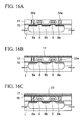
- FIGS. 16A to 16Q are cross-sectional views showing processes of manufacturing a semiconductor device according to a fifth embodiment of the present invention.
- FIGS. 1A to 1O are cross-sectional views showing processes of manufacturing a semiconductor device according to a first embodiment of the present invention.
- a device isolation insulating film 2 is formed by thermally oxidizing a surface of an n-type or a p-type silicon (semiconductor) substrate 1 , and an active region of a transistor is defined by the device isolation insulating film 2 .
- Such a device isolation structure is referred to as local oxidation of silicon (LOCOS).
- LOCOS local oxidation of silicon
- STI shallow trench isolation
- a thermal oxidation film to be a gate insulating film 4 is formed with a thickness of approximately 6 to 7 nm by thermally oxidizing the surface of the active region.
- an amorphous silicon film with a thickness of approximately 50 nm and a tungsten silicide film with a thickness of approximately 150 nm are sequentially formed on an entire upper surface of the silicon substrate 1 .
- a polysilicon film may be formed. After that, these films are patterned by photolithography to form a gate electrode 5 on the silicon substrate 1 .
- Two of the gate electrodes 5 are formed parallel to each other on the p-well 3 , and each of the gate electrodes 5 forms a part of a word line.
- phosphorus as n-type impurities is introduced into a portion of the silicon substrate 1 beside the gate electrodes 5 by ion implantation using the gate electrodes 5 as a mask. Thereby, first and second source/drain extensions 6 a and 6 b are formed.
- an insulating film is formed on the entire upper surface of the silicon substrate 1 , and the insulating film is etched back to be left as insulating sidewalls 7 beside the gate electrodes 5 .
- a silicon oxide film is formed by a chemical vapor deposition (CVD) method, for example.
- first and second source/drain regions (first and second impurity diffusion regions) 8 a and 8 b are formed on the silicon substrate 1 beside the gate electrodes 5 .
- a refractory metal film such as a cobalt film
- a refractory metal film is formed by a sputtering method on the entire upper surface of the silicon substrate 1 . Then, the refractory metal film is heated, and thereby caused to react with silicon. Accordingly, a refractory metal silicide layer 9 , such as a cobalt silicide layer, is formed in the first and second source/drain regions 8 a and 8 b on the silicon substrate 1 . By this refractory metal silicide layer 9 , resistance of the first and second source/drain regions 8 a and 8 b is made lowered.
- the refractory metal layer left unreacted on the device isolation insulating film 2 and the like is removed by wet etching.
- first and second MOS transistors TR 1 , and TR 2 constructed from the gate insulating films 4 , the gate electrodes 5 , the first and second source/drain regions 8 a and 8 b , and the like, are formed in the active region of the silicon substrate.
- a silicon oxynitride (SiON) film is formed with a thickness of approximately 200 nm on the entire upper surface of the silicon substrate 1 by a plasma CVD method.
- the silicon oxynitride film thus formed is used as a cover insulating film 10 .
- a silicon oxide (SiO 2 ) film is formed as a first interlayer insulating film 11 with a thickness of approximately 600 nm on the cover insulating film 10 , by the plasma CVD method using a TEOS (tetra ethoxy silane) gas.
- TEOS tetra ethoxy silane
- first interlayer insulating film 11 is polished by using a chemical mechanical polishing (CMP) method to planarize the upper surface of the first interlayer insulating film 11 .
- CMP chemical mechanical polishing
- anneal with a substrate temperature of 650° C. is carried out on the first interlayer insulating film 11 for 30 minutes so as to degas the first interlayer insulating film 11 .
- an alumina (Al 2 O 3 ) film is formed with a thickness of about 20 nm on the first interlayer insulating film 11 as a lower electrode adhesion film 12 .
- a titanium film or a titanium oxide film may be formed as the lower electrode adhesion film 12 .
- the titanium film can be formed by setting a substrate temperature to be 150° C.
- a platinum film is formed by the sputtering method as a first conductive film 23 on the lower electrode adhesion film 12 .
- the first conductive film 23 will be patterned later to be a capacitor lower electrode.
- the first conductive film 23 is formed at a film-forming temperature of 100° C. or 350° C. to have a thickness of approximately 150 nm.
- the thickness of the first conductive film 23 made of platinum is set at approximately 180 nm.
- a PLZT film made by doping La into the PZT film is formed on the first conductive film 23 as a first ferroelectric film 24 b.
- the sol-gel method is carried out as follows.
- a PLZT-coating film is formed by applying a PLZT solution (ferroelectric solution) onto a first conductive film 23 for 30 seconds by a spin coating method with a rotational frequency of 5000 rpm in an atmosphere with humidity of 40%.
- a PLZT solution ferroelectric solution
- the butanol solvent in the PLZT-coating film is evaporated, and volume of the PLZT-coating film shrinks. Thereby, concentration of gel including molecules constituting a ferroelectric substance increases, and this makes it easier to crystallize the PLZT-coating film later.
- the anneal carried out for evaporating a solvent in this manner is also referred to as bake.
- the ferroelectric film 24 made of PLZT is formed with a thickness of 100 nm by repeating formation of such a PLZT-coating film and bake predetermined times, for example, 3 times.
- the ferroelectric film 24 formed by the sol-gel method is not limited to a PLZT film.
- the first ferroelectric film 24 b may be formed of a ferroelectric material having an ABO 3 -type perovskite structure (A represents any one of Bi, Pb, Ba, Sr, Ca, Na, K, and rare-earth elements, and B represents any one of Ti, Zr, Nb, Ta, W, Mn, Fe, Co, and Cr).
- A represents any one of Bi, Pb, Ba, Sr, Ca, Na, K, and rare-earth elements
- B represents any one of Ti, Zr, Nb, Ta, W, Mn, Fe, Co, and Cr).
- Bi layer structure compounds such as (Bi 1-X R X )Ti 3 O 12 (R represents a rare-earth element with 0 ⁇ x ⁇ 1), SrBi 2 Ta 2 O 9 (SBT) and SrSi 4 Ti 4 O 15 is also made from an ABO 3 -type perovskite structure when viewed as a single unit of crystals. Therefore, the Bi layer structure compounds can also be adopted as a material constituting the first ferroelectric film 24 b.
- the first conductive film 23 be made of a material having a lattice constant close to that of the PZLT constituting the first ferroelectric film 24 b .
- a material having a lattice constant close to that of the PZLT constituting the first ferroelectric film 24 b includes palladium, SrRuO 3 and LaSrCoO 3 having the same perovskite structure as that of the PLZT, in addition to the above-described platinum.
- the first conductive film 23 is not limited to the single-layered film, and it may be a laminated film in which any one of platinum, palladium, SrRuO 3 and LaSrCoO 3 is exposed on the upper surface.
- ruthenium, iridium and oxides of these materials have a lattice constant far from that of the PLZT. Therefore, when the first conductive film 23 is made of these materials, the crystallinity of the first ferroelectric film 24 b may possibly be deteriorated due to lattice mismatch.
- the first ferroelectric film 24 b formed by the sol-gel method is not crystallized at the time the first ferroelectric film 24 b is formed.
- atmospheric-pressure RTA Rapid Thermal Anneal
- crystallization anneal is carried out on the first ferroelectric film 24 b in an atmosphere containing an oxidizing gas so as to crystallize the first ferroelectric film 24 b in a (111) direction in which an amount of polarization charges becomes the largest.
- Such anneal is referred to as crystallization anneal.
- the atmosphere used for the crystallization anneal is not particularly limited as long as it is an atmosphere containing an oxidizing gas.
- the crystallization anneal is carried out in an atmosphere of 100% oxygen.
- an ozone gas or a nitrogen dioxide gas may be used as an oxidizing gas.
- these gases may be diluted with an inert gas such as an argon gas.
- a speed of raising the temperature used for the crystallization anneal is also not limited. However, in the present embodiment, the speed of raising the temperature is set at 40 to 150° C. per minute. To improve the crystallinity of the first ferroelectric film 24 b , it is preferable that the speed of raising the temperature be made as fast as possible, for example, 125° C. per minute.
- an interface in which PZT crystal grains are discontinuous, may be formed in a vicinity of the upper surface of the first ferroelectric film 24 b .
- the layer above this interface is referred to as a surface layer. Unevenness due to the crystal grains is formed on the upper surface of the surface layer. Such unevenness is one of factors for not being able to uniformly apply a voltage to the first ferroelectric film 24 b.
- the lower limit of the maximum substrate temperature used for the above-described crystallization anneal be set at the crystallization temperature of the first ferroelectric film 24 b , and that the upper limit thereof be set at 60° C. higher than the crystallization temperature.
- the maximum substrate temperature is set at 500 to 560° C., for example 550° C.
- the upper limit of the maximum substrate temperature By setting the upper limit of the maximum substrate temperature to be a relatively low temperature in this manner, crystallization develops from the lower surface of the first ferroelectric film 24 b . Hence, the crystal grains of the first ferroelectric film 24 b take over crystallinity of the first conductive film 23 . Accordingly, the above-described surface layer is not easily formed, and the unevenness of the first ferroelectric film 24 b is suppressed.
- this crystallization anneal also makes it possible to obtain an advantage that interdiffusion of platinum and oxygen is suppressed in the vicinity of the interface between the first conductive film 23 and the first ferroelectric film 24 b , since the platinum film constituting the first conductive film 23 is made dense by the crystallization anneal.
- this crystallization anneal may be carried out by reduced-pressure RTA.
- the first ferroelectric film 24 b is more easily crystallized by the reduced-pressure RTA than by the atmospheric-pressure RTA. Therefore, with the reduced-pressure RTA, the upper and lower limits of the substrate temperature can be lower by respectively about 10° C. and 5° C. than with the atmospheric pressure RTA.
- a PZT film is formed with a thickness of about 1 to 50 nm, more preferably 10 to 30 nm, on the first ferroelectric film 24 b by the sputtering method.
- This PZT film is used as a second ferroelectric film 24 c.
- the sputtering method has an advantage that a small amount of an additive element can easily be doped to the second ferroelectric film 24 c.
- any one of strontium, calcium, niobium, iridium, and lanthanum be added to the PZT as an additive element with a concentration of 0.1 to 5 mol %.
- calcium, lanthanum, and strontium are respectively doped into the PZT with concentrations of 5 mol %, 2 mol %, and 2 mol %, and thereby the switching charge of the second ferroelectric film 24 c is increased.
- the PZT to which calcium, lanthanum and strontium are added in this manner is written as CSPLZT.
- a material of the second ferroelectric film 24 c is not limited to the PZT, as long as the material is a ferroelectric material having an ABO 3 -type perovskite structure (A represents any one of Bi, Pb, Ba, Sr, Ca, Na, K and rare-earth elements, and B represents any one of Ti, Zr, Nb, Ta, W, Mn, Fe, Co and Cr).
- A represents any one of Bi, Pb, Ba, Sr, Ca, Na, K and rare-earth elements
- B represents any one of Ti, Zr, Nb, Ta, W, Mn, Fe, Co and Cr.
- the second ferroelectric film 24 c may be constructed from Bi layer structure compounds such as (Bi 1-X R X )Ti 3 O 12 (R represents a rare-earth element with 0 ⁇ x ⁇ 1), SrBi 2 Ta 2 O 9 (SBT) and SrBi 4 Ti 4 O 15 .
- Bi layer structure compounds such as (Bi 1-X R X )Ti 3 O 12 (R represents a rare-earth element with 0 ⁇ x ⁇ 1), SrBi 2 Ta 2 O 9 (SBT) and SrBi 4 Ti 4 O 15 .
- a ferroelectric film 24 made of the first and second ferroelectric films 24 b and 24 c is formed on the first conductive film 23 .
- the first ferroelectric film 24 b is formed by the sol-gel method with which costs for forming a film is low, and which thus contributes to cost reduction for a semiconductor device.
- the second ferroelectric film 24 c contributes to planarizing the upper surface of the entire ferroelectric film 24 by burying the unevenness of the upper surface of the first ferroelectric film 24 b which is generated due to the PZT crystal grains. In this manner, the second ferroelectric film 24 c is formed to achieve planarization rather than to gain a film thickness of the ferroelectric film 24 . Therefore, it is preferable that the second ferroelectric film 24 c be formed thinner than the first ferroelectric film 24 b to burden the first ferroelectric film 24 b with the most of the ferroelectric characteristics of the ferroelectric film 24 .
- an iridium oxide film which is already crystallized at the time of depositing, is formed with a thickness of approximately 25 nm on the above-described ferroelectric film 24 , by the sputtering method which uses the mixed gas of oxygen and argon as a sputtering gas, and which uses an iridium target.
- This iridium oxide film is used as a first conductive metal oxide film 25 d.
- an interface between the second ferroelectric film 24 c and the first conductive metal oxide film 25 d is made substantially flat by forming the second ferroelectric film 24 c by the sputtering method as described above. Accordingly, a paraelectric layer due to interdiffusion of these films 24 c and 25 d is less likely to be formed in the interface, and thus it is possible to prevent an occupying ratio of the ferroelectric substance in the ferroelectric film 24 from being reduced.
- the first conductive metal oxide film 25 d is already crystallized at the time of forming thereof, an interface between the first conductive metal oxide film 25 d and the second ferroelectric film 24 c is clearly formed, and thus the above-described paraelectric film is less likely to be formed in the vicinity of the interface.
- a substrate temperature be set at 300° C. or more.
- crystallization does not sufficiently develop at the time of film forming, so that the iridium oxide film may possibly be in an amorphous state.
- a flow rate of argon is set at 140 sccm, and a flow rate of oxygen is set at 60 sccm.
- Sputtering power is set at 1 to 2 kW.
- RTA is carried out on the first conductive metal oxide film 25 d in the mixed atmosphere of an oxygen gas and an argon gas.
- the gas flow rate in this RTA is not particularly limited.
- the flow rate of oxygen is set at 20 sccm
- the flow rate of argon is set at 2000 sccm.
- the ferroelectric film 24 is completely crystallized, and damages received in the ferroelectric film 24 at the time of forming the first conductive metal oxide film 25 d by the sputtering method are recovered. Moreover, the oxygen loss in the ferroelectric film 24 is also compensated by this RTA, and ferroelectric characteristics of the ferroelectric film 24 improve.
- This anneal also provides an advantage in that a voltage can be uniformly applied from an upper electrode to be described later, to the ferroelectric film 24 , since the interface between the first conductive metal oxide film 25 d and the ferroelectric film 24 is made flat.
- the anneal atmosphere at this time is not particularly limited as long as it is an atmosphere containing an oxidizing gas.
- the examples of the oxidizing gas include an ozone gas and a nitrogen dioxide gas, in addition to the above-described oxygen gas.
- an iridium oxide film is formed with a thickness of approximately 200 nm as a second conductive metal oxide film 25 e on the first conductive metal oxide film 25 d .
- an iridium target is used, and the mixed gas of oxygen and argon is used as a sputtering gas.
- an iridium oxide film constituting the second conductive metal oxide film 25 e needs not be crystallized at the time of film forming.
- a substrate temperature at the time of forming the second conductive metal oxide film 25 e is set to be room temperature (20° C.) so as to form an iridium oxide film in an amorphous state.
- the deposited iridium oxide includes iridium atoms which are not sufficiently oxidized in the atmosphere, so that an entire iridium oxide film is easily set in a state where the amount of oxygen is less than that of stoichiometry composition (IrO 2 ).
- an oxidation number of the second conductive metal oxide film 25 e be larger than that of the first conductive metal oxide film 25 d.
- the composition of iridium oxide is brought close to stoichiometry composition (IrO 2 ), so that the catalysis of the second conductive metal oxide film 25 e would be suppressed.
- the flow rate ratio of oxygen in the present specification is defined as a percentage of a flow rate of oxygen in an entire flow rate of the sputtering gas.
- a second conductive film 25 constructed from the first and second conductive metal oxide films 25 d and 25 e is formed on the ferroelectric film 24 .
- first and second conductive metal oxide films 25 d and 25 e is not limited to iridium oxide.
- the first and second conductive metal oxide films 25 d and 25 e may be formed of an oxide of any one of iridium, ruthenium, rhodium, rhenium, and osmium. Furthermore, these oxides may be stacked as the second conductive film 25 .
- the first conductive film 25 is patterned by photolithography and etching to form an upper electrode 25 a .
- recovery anneal is carried out on the ferroelectric film 24 in a vertical furnace. This recovery anneal is carried out in an atmosphere containing oxygen, and conditions thereof are, for example, a substrate temperature of 650° C., and a processing time of 60 minutes.
- the ferroelectric film 24 is patterned by photolithography and etching to form a capacitor dielectric film 24 a made of a ferroelectric material such as PLZT. Damages received in the capacitor dielectric film 24 a due to this patterning are recovered by recovery anneal. As in the case described above, this recovery anneal is carried out by using the vertical furnace in an atmosphere containing oxygen, and adopted conditions thereof are a substrate temperature of 350° C. and a processing time of 60 minutes.
- a first alumina film 31 for protecting the capacitor dielectric film 24 a from reductants such as hydrogen and moisture is formed with a thickness of approximately 50 nm on the entire upper surface of the silicon substrate 1 by the sputtering method.
- the recovery anneal described in FIG. 1H is carried out in advance, the first alumina film 31 is less likely to be peeled off.
- recovery anneal is carried out in the atmosphere containing oxygen with a substrate temperature of 550° C. for approximately 60 minutes. This recovery anneal is carried out by using, for example, a vertical furnace.
- the first conductive film 23 and the first alumina film 31 are patterned by photolithography and etching, and thereby the first conductive film 23 below the capacitor dielectric film 24 a is used as a lower electrode 23 a .
- the first alumina film 31 is left to cover the lower electrode 23 a.
- the lower electrode 23 a has a contact region CR protruding from the capacitor dielectric film 24 a .
- this contact region CR a metal wiring to be described later, and the lower electrode 23 a are electrically connected to each other.
- the recovery anneal is carried out to the capacitor dielectric film 24 a in the atmosphere containing oxygen in the vertical furnace under conditions with a substrate temperature of 550° C. and a processing time of 60 minutes.
- a second alumina film 32 for protecting the capacitor dielectric film 24 a is formed with a thickness of approximately 20 nm on the entire upper surface of the silicon substrate 1 by the sputtering method.
- This second alumina film 32 together with the first alumina film 31 thereunder, prevents reductants, such as hydrogen and moisture, from coming in contact with the capacitor dielectric film 24 a , and has a function of suppressing deterioration of ferroelectric characteristics of the capacitor dielectric film 24 a due to reduction thereof.
- the recovery anneal is carried out on the capacitor dielectric film 24 a in the vertical furnace with the atmosphere containing oxygen, under conditions with a substrate temperature of 550° C. and a processing time of 60 minutes.
- This recovery anneal also provides an advantage that a leak current of the capacitor Q is reduced.
- a silicon oxide film is formed with a thickness of approximately 1500 nm on the above-described second alumina film 32 by a high-density plasma CVD (HDPCVD) method using a silane (SiH 4 ) gas, and the silicon oxide film is used as a second interlayer insulating film 41 . Thereafter, an upper surface of the second interlayer insulating film 41 is polished and planarized by the CMP method.
- HDPCVD high-density plasma CVD
- the second interlayer insulating film 41 is dehydrated by performing N 2 O plasma processing on the second interlayer insulating film 41 , and the upper surface of the second interlayer insulating film 41 is slightly nitrided, and thereby moisture is prevented from being absorbed again into the second interlayer insulating film 41 .
- insulating films 10 to 12 , 31 , 32 , and 41 are patterned by photolithography and dry etching to form first and second contact holes 41 a and 41 b in these films on the first and second source/drain regions 8 a and 8 b.
- a titanium film and a titanium nitride film are formed respectively with thicknesses of 20 nm and 50 nm, by the sputtering method, and these films are used as a glue film (an adhesion film).
- a tungsten film is formed on the glue film by a CVD method using a tungsten hexafluoride gas, and the first and second contact holes 41 a and 41 b are completely embedded with this tungsten film.
- the excessive glue film and tungsten film on the second interlayer insulating film 41 are polished and removed by the CMP method, and these films are left only inside the first and second contact holes 41 a and 41 b as first and second conductive plugs 61 a and 61 b .
- the first and second conductive plugs 61 a and 61 b are electrically connected to the first and second source/drain regions 8 a and 8 b , respectively.
- the first and second conductive plugs 61 a and 61 b are mainly formed of tungsten which is oxidized very easily. Therefore, the first and second conductive plugs 61 a and 61 b are easily oxidized in the atmosphere containing oxygen, so that these plugs may possibly induce contact defect.
- a silicon oxynitride film is formed by the CVD method with a thickness of approximately 100 nm as an antioxidant insulating film 55 on the entire upper surface of the silicon substrate 1 .
- the antioxidant insulating film 55 protects the first and second conductive plugs 61 a and 61 b from being oxidized.
- the silicon substrate 1 is put in the vertical furnace with the atmosphere containing oxygen, and the recovery anneal is carried out on the capacitor dielectric film 24 a under conditions with a substrate temperature of 500° C. and a processing time of 60 minutes.
- a metal laminated film is formed by the sputtering method on each of the upper surfaces of the second interlayer insulating film 41 and the first and second conductive plugs 61 a and 61 b .
- a titanium nitride film with a thickness of approximately 150 nm a titanium nitride film with a thickness of approximately 150 nm, a copper-containing aluminum film with a thickness of approximately 550 nm, a titanium film with a thickness of approximately 5 nm, and a titanium nitride film with a thickness of approximately 150 nm are formed in this order.
- This metal laminated film is also formed in the third and fourth holes 41 c and 41 d on the capacitor Q.
- the metal laminated film is patterned by photolithography and etching to form a metal wiring 62 electrically connected to the capacitor Q and to the conductive plugs 61 a and 61 b.
- anneal is carried out to dehydrate the second interlayer insulating film 41 under conditions with a substrate temperature of 350° C., a flow rate of N 2 at 20 liter per minute, and a processing time of 30 minutes, by using the vertical furnace with, for example, a nitrogen atmosphere.
- the PZT film is formed by the sputtering method as the second ferroelectric film 24 c.
- the interface between the second ferroelectric film 24 c and the first conductive metal oxide film 25 d is made substantially flat.
- a paraelectric layer due to interdiffusion of these films 24 c and 25 d is less likely to be formed in the above interface.
- the occupying ratio of the above-described paraelectric layer in the capacitor dielectric film 24 a can be reduced, so that the most of the capacitor dielectric film 24 a can be formed of a ferroelectric substance. Accordingly, it is made possible to increase the switching charge of the capacitor Q, and to form the capacitor Q which is extremely useful for a next-generation FeRAM capable of being operated at a low voltage.
- the interface between the second ferroelectric film 24 c and the first conductive metal oxide film 25 d is made stable. Thereby, it is made possible to effectively prevent the formation of an interface layer due to the interdiffusion of these films 24 c and 25 d.
- FIGS. 2A to 2X are cross-sectional views showing processes of manufacturing a semiconductor device according to the present embodiment.
- This semiconductor device is a stacked-type FeRAM advantageous for miniaturization, and is formed as follows.
- a groove for STI which defines an active region of a transistor, is initially formed on a surface of an n-type or p-type silicon substrate 1 . Then, an insulating film such as silicon oxide film is embedded therein as a device isolation insulating film 2 .
- a device isolation structure is not limited to STI, and a device isolation insulating film 2 may be formed by a LOCOS method.
- first and second MOS transistors TR 1 , and TR 2 formed of gate insulating films 4 , gate electrodes 5 , first and second source/drain regions 8 a and 8 b , and the like, are formed in the active region of the silicon substrate 1 .
- a silicon nitride (SiN) film is formed with a thickness of approximately 80 nm on an entire upper surface of the silicon substrate 1 by a plasma CVD method, and is set to be a cover insulating film 10 .
- a silicon oxide film is formed with a thickness of approximately 1000 nm, as a first interlayer insulating film 11 by a plasma CVD method using a TEOS gas.
- the upper surface of the first interlayer insulating film 11 is polished and planarized by a chemical mechanical polishing (CMP) method.
- CMP chemical mechanical polishing
- the cover insulating film 10 and the first interlayer insulating film 11 are patterned by photolithography to form contact holes each with a diameter of 0.25 ⁇ m on the first and second source/drain regions 8 a and 8 b . Furthermore, a glue film and a tungsten film are sequentially formed in each of the contact holes. After that, the excessive glue film and tungsten film on the first interlayer insulating film 11 are polished and removed by the CMP method, and these films are left only in the contact holes as first and second conductive plugs 32 a and 32 b.
- the first and second conductive plugs 32 a and 32 b are electrically connected to the first and second source/drain regions 8 a and 8 b , respectively.
- the above-described glue film is made by forming a titanium film with a thickness of approximately 30 nm and a titanium nitride film with a thickness of approximately 20 nm in this order.
- the tungsten film before the CMP has a thickness of approximately 300 nm on the first interlayer insulating film 11 .
- first and second conductive plugs 32 a and 32 b are mainly formed of tungsten which is easily oxidized, contact defect may be caused when the first and second conductive plugs 32 a and 32 b are oxidized during the manufacturing processes.
- a silicon oxynitride film is formed with a thickness of approximately 130 nm on the conductive plugs 32 a and 32 b and on the first interlayer insulating film 11 by the plasma CVD method.
- a silicon nitride film or an alumina film may be formed as the antioxidant insulating film 14 .
- a silicon oxide film is formed with a thickness of approximately 300 nm on the antioxidant insulating film 14 by the plasma CVD method using a TEOS gas. This silicon oxide film is used as a base insulating film 15 .
- the base insulating film 15 and the antioxidant insulating film 14 are patterned, and thus first holes 15 a are formed in these insulating films above the first conductive plugs 32 a.
- a titanium nitride film is formed as a glue film 35 in the first contact holes 15 a and on the base insulating film 15 by the sputtering method.
- a tungsten film is formed on this glue film 35 as a plug conductive film 36 by the CVD method, and then the first holes 15 a are completely embedded with the plug conductive film 35 .
- the excessive glue film 35 and plug conductive film 36 on the base insulating film 15 are polished and removed by the CMP method.
- the glue film 35 and the plug conductive film 36 are left in the first holes 15 a as third conductive plugs 36 a electrically connected to the first conductive plugs 32 a.
- a polishing speed for the glue film 35 and for the plug conductive film 36 are faster than that for the base insulating film 15 .
- W2000 manufactured by Cabot Microelectronics Corporation is used.
- a polishing amount in this CMP is set thicker than the total film thickness of the films 35 and 36 , so that over-polishing is performed in this CMP.
- the base insulating film 15 made of silicon oxide is exposed to plasma containing nitrogen, such as ammonia (NH 3 ) plasma, to bond an NH group with each oxygen atom on the surface of the base insulating film 15 .
- nitrogen such as ammonia (NH 3 ) plasma
- Equipment used for this ammonia plasma processing is, for example, a parallel plate-type plasma processing equipment having an opposing electrode in a position away from the silicon substrate by approximately 9 mm (350 mils). Then, this processing is carried out in the following manner. Specifically, while maintaining a substrate temperate at 400° C. under the pressure of 266 Pa (2 Torr), an ammonia gas is supplied to the inside of a chamber with a flow rate of 350 sccm, and high frequency power of 13.56 MHz and 350 kHz are respectively supplied, for 60 seconds, to the silicon substrate 1 with power of 100 W and to the above-described opposed electrode with power of 55 W.
- a titanium film is formed with a thickness of approximately 20 nm on each of the base insulating film 15 and the third conductive plugs 36 a .
- This titanium film is used as a conductive adhesion film 16 .
- the film-forming conditions for the conductive adhesion film 16 are not particularly limited.
- the substrate temperature is set at 20° C. in the argon atmosphere of 0.15 Pa by using a sputtering chamber in which a distance between the silicon substrate 1 and a titanium target is set to be 60 mm. Then, DC power at 2 . 6 kW is supplied to the chamber for 5 seconds to form the conductive adhesion film 16 made of titanium.
- the ammonia plasma processing (see FIG. 2D ) is carried out in advance to bond the NH group with each oxygen atom on the surface of the base insulating film 15 . Therefore, titanium atoms deposited on the base insulating film 15 are less likely to be captured by the oxygen atoms on the surface of the base insulating film 15 . For this reason, the titanium atoms can freely move on the surface of the base insulating film 15 , and thus it is made possible to form the conductive adhesion film 16 made of titanium whose crystalline orientation is strongly self-oriented in a (002) direction.
- RTA rapid thermal anneal
- a material of the conductive adhesion film 16 is not limited to titanium nitride.
- the conductive adhesion film 16 may be formed of any one of titanium, titanium nitride, platinum, iridium, rhenium, ruthenium, palladium, rhodium, and osmium, or an alloy thereof.
- the conductive adhesion film 16 may be formed of any one of platinum oxide, iridium oxide, ruthenium oxide and palladium oxide.
- TiAlN titanium aluminum nitride
- the conductive oxygen barrier film 17 made of titanium aluminum nitride is superior in a function of preventing oxygen from being permeated, and plays a role of preventing occurrence of contact defect due to oxidation of the third conductive plugs 36 a thereunder.
- the film-forming conditions for the conductive oxygen barrier film 17 are not particularly limited.
- an alloy target of titanium and aluminum is used, and the mixed gas of an argon gas and a nitrogen gas is used for a sputtering gas.
- the conductive oxygen barrier film 17 is formed under conditions with the flow rates of the argon gas and the oxygen gas at respectively 40 sccm and 100 sccm, pressure at 253.3 Pa, a substrate temperature at 400° C., and sputtering power at 1.0 kW.
- the material of the conductive oxygen barrier film 17 is not limited to titanium aluminum nitride.
- the conductive oxygen barrier film 17 may be made of any one of titanium aluminum nitride, titanium aluminum oxynitride (TiAlON), tantalum aluminum nitride (TaAlN), and tantalum aluminum oxynitride (TaAlON).
- the adhesion strength of the conductive oxygen barrier film 17 with the base is increased with the conductive adhesion film 16 . If adhesion strength is not considered to be a problem, the conductive adhesion film 16 may be omitted. In this case, the conductive oxygen barrier film 17 is directly formed on each of the upper surfaces of the third conductive plugs 36 a and the base insulating film 15 .
- an iridium film is formed with a thickness of approximately 100 nm as a first conductive film 23 on the conductive oxygen barrier film 17 by the sputtering method.
- the film-forming conditions of the iridium film are not particularly limited.
- the iridium film is formed by using an argon gas as a sputtering gas, and by applying sputtering power of 0.5 kW to the sputtering atmosphere under pressure of 0.11 Pa with a substrate temperature of 500° C.
- RTA with a substrate temperature of 650° C. or more is carried out on the first conductive film 23 in the argon atmosphere for 60 seconds.
- this RTA adhesion between the first conductive film 23 and the conductive oxygen barrier film 17 improves, and crystallinity of the first conductive film 23 also improves.
- this RTA may be carried out in a nitrogen atmosphere.
- a PZT film is formed with a thickness of approximately 80 nm on the first conductive film 23 by the MOCVD method, and the PZT film is used as a main ferroelectric film 24 d.
- the MOCVD method is carried out as follows.
- the silicon substrate 1 is mounted on a susceptor in an unillustrated reaction chamber.
- oxygen is introduced into the reaction chamber, and a temperature of the silicon substrate 1 is increased to be stabilized at about 620° C.
- a vaporized THF solvent is introduced into the reaction chamber. Thereby, the first conductive film 23 is exposed to the atmosphere of the solvent gas.
- the source gas is prevented from being solidified in a vaporizer or in a pipe.
- problems such as clogging of the pipe, can be avoided.
- vaporized butyl acetate may be used as the solvent gas.
- each of liquid sources of Pb, Zr, and Ti is vaporized in the vaporizer to form the source gas, and the forming of the PZT film is started by introducing each source gas into the reaction chamber.
- each liquid source may be made, for example, by dissolving each of Pb(DPM) 2 (chemical formula: Pb(C 11 H 19 O 2 ) 2 ), Zr(dmhd) 4 (chemical formula: Zr(C 9 H 15 O 2 ) 4 ), and Ti (O-iOr) 2 (DPM) 2 (chemical formula: Ti(C 3 H 7 O) 2 (C 11 H 19 O 2 ) 2 ) into a TFH (Tetra Hydro Furan: C 4 H 8 O) solvent with a concentration of 0.3 mol/l.
- a flow rate of the vaporized source gas is not particularly limited.
- the source gases of Pb, Zr, and Ti are obtained by supplying the above-described liquid sources to the vaporizer respectively with the flow rates of 0.32 ml per minute, 0.200 ml per minute, and 0.200 ml per minute, and then by vaporizing thereof.
- the main ferroelectric film 24 d formed by the MOCVD method in this manner is already crystallized at the time of film forming, and the crystalline orientation thereof is aligned in the (111) direction. Accordingly, crystallization anneal for crystallizing the main ferroelectric film 24 d is not necessary.
- the use of the MOCVD method prevents ferroelectric characteristics of the main ferroelectric film 24 d from being deteriorated even when the main ferroelectric film 24 d is made thinner. This is an advantage in fabricating highly-integrated semiconductor devices. Such an advantage is easily obtained particularly in the stacked-type FeRAM of the present embodiment, which is advantageous for higher integration of capacitors.
- the silicon substrate 1 needs to be heated to high temperature for forming the film by the MOCVD method.
- the constituting materials of the first conductive film 23 are thermally diffused to the main ferroelectric film 24 d due to the heat, the ferroelectric characteristics, such as the switching charge, of the main ferroelectric film 24 d are deteriorated.
- Such a problem is notably caused in the case where a platinum film is formed as the first conductive film 23 . Therefore, it is preferable to avoid forming a platinum film as the first conductive film 23 .
- the first conductive film 23 is made of iridium as in the present embodiment, the deterioration of the main ferroelectric film 24 d due to the thermal diffusion is hardly observed. In addition, the deterioration of the main ferroelectric film 24 d due to thermal diffusion can be also prevented by forming the first conductive film 23 of ruthenium.
- the main ferroelectric film 24 d is formed by the MOCVD method, it is preferable that a conductive film of which any one of iridium and ruthenium is exposed onto the upper surface be formed as the first conductive film 23 .
- the above-described deterioration of the main ferroelectric film 24 d can be also prevented by forming, as the first conductive film 23 a , conductive film of which any one of SrRuO 3 and LaSrCoO 3 is exposed on the upper surface.
- an auxiliary ferroelectric film 24 e is formed by the sol-gel method with a thickness of approximately 20 nm on the main ferroelectric film 24 d , and thus the unevenness of the upper surface of the main ferroelectric film 24 d is buried with the auxiliary ferroelectric film 24 e.
- the unevenness of the upper surface of the auxiliary ferroelectric film 24 e becomes smaller than that of the upper surface of the main ferroelectric film 24 d which is formed by the MOCVD method.
- the RMS (surface roughness) of the main ferroelectric film 24 d is typically about 10 nm
- the RMS of the auxiliary ferroelectric film 24 e becomes about 6 to 7 nm.
- the auxiliary ferroelectric film 24 e is formed by the sol-gel method under the same conditions as the first ferroelectric film 24 b described in the first embodiment, and the solution obtained by dissolving each of precursors of Pb, La, Zr and Ti in a butanol solvent with a concentration of 10 weight % is used. Then, the solution is applied onto the main ferroelectric film 24 d by the spin coating method, so that one layer of PLZT-coating film is formed. After that, bake is carried out in the oxygen atmosphere of atmospheric pressure with a substrate temperature of 200 to 450° C., for example, 240° C., for approximately 5 minutes. Thereby, the above-described auxiliary ferroelectric film 24 e is obtained.
- the first ferroelectric film 24 b constructed from the main ferroelectric film 24 d and the auxiliary ferroelectric film 24 e is formed on the first conductive film 23 .
- the auxiliary ferroelectric film 24 e formed by the sol-gel method is formed for the purpose of embedding the unevenness of the upper surface of the main ferroelectric film 24 d . Therefore, it is preferable that the auxiliary ferroelectric film 24 e have a thickness thinner than that of the main conductive ferroelectric film 24 d , so that the first ferroelectric film 24 b is mainly formed of the main ferroelectric film 24 d.
- auxiliary ferroelectric film 24 e formed by the sol-gel method is not limited to the PLZT film.
- the auxiliary ferroelectric film 24 e may be formed of a ferroelectric material having an ABO 3 -type perovskite structure (A represents any one of Bi, Pb, Ba, Sr, Ca, Na, K, and rare-earth elements, and B represents any one of Ti, Zr, Nb, Ta, W, Mn, Fe, Co, and Cr) as in PLZT.
- A represents any one of Bi, Pb, Ba, Sr, Ca, Na, K, and rare-earth elements
- B represents any one of Ti, Zr, Nb, Ta, W, Mn, Fe, Co, and Cr
- Bi layer structure compounds such as (Bi 1-X R X )Ti 3 O 12 (R is a rare-earth element with 0 ⁇ x ⁇ 1), SrBi 2 Ta 2 O 9 (SBT) and SrBi 4 Ti 4 O 15 may be used as a material forming the auxiliary ferroelectric film 24 e.
- the main ferroelectric film 24 d may be formed by the metal organic deposition (MOD) method.
- auxiliary ferroelectric film 24 e formed by the sol-gel method is not crystallized at the time of film forming. For this reason, auxiliary ferroelectric film 24 e has poor ferroelectric characteristics in this state.
- crystallization anneal is carried out on the auxiliary ferroelectric film 24 e in the atmosphere containing oxygen to crystallize the auxiliary ferroelectric film 24 e.
- the crystallization anneal is carried out by atmospheric-pressure RTA. Then, oxygen and argon, both of which have a flow rate of 1000 sccm, are supplied to the anneal atmosphere to carry out crystallization anneal for a processing time of 30 to 120 seconds, for example, 90 seconds.
- a speed of raising a temperature for the crystallization anneal is also not particularly limited.
- the speed of raising a temperature is set at 40 to 150° C. per minute.
- the speed of raising the temperature be set to be as fast as possible, for example, 125° C. per minute.
- the surface layer described in the first embodiment is formed in the auxiliary ferroelectric film 24 e .
- the crystal grains of the auxiliary ferroelectric film 24 e and the crystal grains of the main ferroelectric film 24 d may possibly not be bonded with each other.
- the lower limit of the maximum substrate temperature for the above-described anneal be set at a crystallization temperature of the auxiliary ferroelectric film 24 e , and that the upper limit thereof be set to be a temperature 60° C. higher than the crystallization temperature.
- the maximum substrate temperature is set at 500 to 560° C., for example 550° C.
- the crystallization develops from the lower surface of the auxiliary ferroelectric film 24 e .
- the crystal grains of the auxiliary ferroelectric film 24 e take over the crystal grains of the main ferroelectric film 24 d . Accordingly, an interface is not easily formed between the ferroelectric films 24 d and 24 e , and unevenness of the auxiliary ferroelectric film 24 e is suppressed.
- a PZT film is formed as a second ferroelectric film 24 c on the first ferroelectric film 24 b by the sputtering method. It is preferable that a thickness of the second ferroelectric film 24 c be set at 1 to 50 nm, more preferably 10 to 30 nm, which is thinner than the thickness of the first ferroelectric film 24 b.
- any one of strontium, calcium, niobium, iridium, and lanthanum be used as an additive element to be added to the PZT, with a concentration of 0.1 to 5 mol %, at the time of forming the second ferroelectric film 24 c in order to improve the ferroelectric characteristics of the second ferroelectric film 24 c .
- the PZT is doped with calcium, lanthanum and strontium respectively with concentrations of 5 mol %, 2 mol %, and 2.5 mol %.
- a ferroelectric film 24 constructed from the first and second ferroelectric films 24 b and 24 c is formed on the first conductive film 23 .
- an iridium oxide film is formed with a thickness of approximately 25 nm as a first conductive metal oxide film 25 d on the ferroelectric film 24 by the sputtering method, while heating the silicon substrate 1 .
- the iridium oxide film formed by the sputtering method in which the silicon substrate 1 is heated is already crystallized at the time of forming thereof without carrying out a process for crystallization of the iridium oxide film.
- the film-forming conditions of the first conductive metal oxide film 25 d are not particularly limited.
- conditions are as follows. Specifically, while maintaining the substrate temperature at 300° C., the iridium target is used, and the mixed gas of an oxygen gas at the flow rate of 140 sccm and the argon gas at the flow rate of 60 sccm is used as a sputtering gas.
- the sputtering power is set at 1 to 2 kW.
- the ferroelectric film 24 may have been damaged by the sputtering gas at the time of forming the first conductive metal oxide film 25 d by the sputtering method, and have insufficient oxygen concentration in the film. Therefore, ferroelectric characteristics of ferroelectric film 24 may possibly be deteriorated.
- the conditions for this RTA are not particularly limited.
- a substrate temperature is set at 725° C.
- a processing time is set to be 60 seconds.
- flow rates of argon and oxygen are respectively set at 2000 sccm and 20 sccm.
- the examples of the oxidizing gas in this RTA includes an ozone gas or a nitrogen dioxide gas, in addition to an oxygen gas.
- the first conductive metal oxide film 25 d is crystallized at the time of film forming. Therefore, unevenness is formed in an interface between the first conductive metal oxide film 25 d and the ferroelectric film 24 , due to the crystal grains of the first conductive metal oxide film 25 d .
- This RTA can also provide an advantage that such unevenness can be planarized.
- an iridium oxide film is formed by the sputtering method with a thickness of approximately 100 to 300 nm, for example, 200 nm, as a second conductive metal oxide film 25 e on the first conductive metal oxide film 25 d .
- the second conductive metal oxide film 25 e is formed in the argon atmosphere having pressure of 0.8 Pa with the sputtering power set at 1.0 kW and a film-forming time for 79 seconds.
- the second conductive metal oxide film 25 e formed by the sputtering method with a substrate temperature at room temperature is made to be in an amorphous state.
- This second conductive metal oxide film 25 e is formed in order to prevent the ferroelectric film 24 from being deteriorated. Therefore, it is preferable that an oxidation number of iridium oxide constituting the second conductive metal oxide film 25 e be set as large as possible so as to suppress the reducing action of the second conductive metal oxide film 25 e against water. To increase the oxidation number in this manner, it suffices that a flow rate ratio of oxygen in the sputtering gas be increased in comparison with that in the case of forming the first conductive metal oxide film 25 d . With this process, iridium grains flying from the iridium target are sufficiently oxidized in the sputtering atmosphere. Thus, it is made possible to form an iridium oxide film with an oxidation number close to that of stoichiometry composition (IrO 2 ).
- a conductive metal oxide film 25 b is constructed from the second conductive metal oxide film 25 e and the first conductive metal oxide film 25 d as shown in FIG. 5K .
- the material constituting the first and second conductive metal oxide films 25 d and 25 e is not limited to iridium oxide.
- the first and second conductive metal oxide films 25 d and 25 e may be formed of an oxide of any one of iridium, ruthenium, rhodium, rhenium, and osmium. Furthermore, these oxides may be stacked as the conductive metal oxide film 25 b.
- an iridium film is formed with a thickness of 50 to 100 nm on the conductive metal oxide film 25 b as a conductivity enhancing film 25 c by the sputtering method.
- the sputtering method is carried out in the argon atmosphere with the pressure of 1 Pa, and the sputtering power of 1.0 kW is applied to the sputtering atmosphere.
- the conductivity enhancing film 25 c constitutes a second conductive film 25 , and plays a role of compensating the conductivity of the second conductive film 25 , which tends to be insufficient when the film 25 is constructed from the conductive metal oxide film 25 b alone.
- the conductivity enhancing film 25 c is not limited to the iridium film.
- the conductivity enhancing film 25 c may be formed of any one of iridium, platinum, ruthenium, rhodium, rhenium, osmium, and palladium, or an oxide thereof.
- a titanium nitride film is formed on the second conductive film 25 by the sputtering method, and the titanium nitride film is set to be a first mask material layer 26 .
- a silicon oxide film is formed as a second mask material layer 27 on the first mask material layer 26 by using the plasma CVD method using a TEOS gas.
- the second mask material layer 27 is patterned to form second hard masks 27 a of an island-shape.
- a first hard mask 26 a is formed by etching the first mask material layer 26 while using the second hard mask 27 a as a mask.
- portions of the films 23 to 25 not covered with the first and second hard masks 26 a and 27 a are patterned by dry etching.
- the first conductive film 23 , the ferroelectric film 24 , and the second conductive film 25 are respectively made to be a lower electrode 23 a , a capacitor dielectric film 24 a , and an upper electrode 25 a , which form ferroelectric capacitor Q.
- a gas for the dry etching is not particularly limited, and the mixed gas of HBr and oxygen is used as the etching gas for the first and second conductive films 23 and 25 .
- the mixed gas of chlorine and argon is used as the etching gas for the ferroelectric film 24 .
- a C 4 F 8 gas may be added to these gases.
- the conductive oxygen barrier film 17 has etching tolerance against the etching gas for the first conductive film 23 . Therefore, the conductive oxygen barrier film 17 is left on the entire surface of the conductive adhesion film 16 even after the capacitors Q are formed.
- Each of the capacitors Q formed in this manner is electrically connected to the corresponding first conductive plug 32 a via the conductive oxygen barrier film 17 , the conductive adhesion film 16 , and the third conductive plug 36 a.
- the second hard mask 27 a formed of silicon oxide is removed by wet etching. Note that the second hard mask 27 a may be removed by dry etching.
- the conductive adhesion film 16 and the conductive oxygen barrier film 17 are etched, and these films are left only under each capacitor Q.
- This etching is carried out with dry etching, and the mixed gas of argon and chlorine, for example, is used as an etching gas.
- first hard masks 26 a are also etched by the etching gas. As a result, the first hard masks 26 a are removed when the etching is completed, and an upper surface of the upper electrode 25 a is exposed.
- an alumina film covering each capacitor Q is formed with a thickness of approximately 20 nm, and this alumina film is used as a first capacitor protective insulating film 39 .
- Alumina constituting the first capacitor protective insulating film 39 has an excellent capability of preventing hydrogen from permeated. Thus, hydrogen in the outside is blocked by this first capacitor protective insulating film 39 , and thereby deterioration of the capacitor dielectric film 24 a due to hydrogen can be prevented.
- the capacitor dielectric films 24 a have received damages due to dry etching at the time of forming the capacitors Q (see FIG. 20 ) and by the sputtering method at the time of forming the first capacitor protective insulating film 39 .
- recovery anneal is carried out on the capacitor dielectric film 24 a in the atmosphere containing oxygen.
- the conditions for this recovery anneal are not particularly limited.
- a substrate temperature is set at 550 to 700° C., for example, 650° C. in a furnace, and a processing time is set to be approximately 60 minutes.
- an alumina film is formed with a thickness of approximately 20 nm on the first capacitor protective insulating film 39 by the CVD method.
- This alumina film is used as a second capacitor protective insulating film 40 .
- a silicon oxide film is formed as a second interlayer insulating film 41 on the second capacitor protective insulating film 40 by plasma CVD using a TEOS gas as a reactant gas.
- the reactant gas includes an oxygen gas and a helium gas.
- the thickness of the second interlayer insulating film 41 is not particularly limited. In the present embodiment, the thickness on the flat surface of the silicon substrate 1 is set to be 1500 nm.
- an insulating inorganic film may be formed as the second interlayer insulating film 41 .
- the surface of the second interlayer insulating film 41 is polished and planarized by the CMP method.
- the surface of the second interlayer insulating film 41 is exposed to N 2 O plasma as dehydration processing to the second interlayer insulating film 41 .
- N 2 O plasma moisture remaining inside the second interlayer insulating film 41 is removed, and moisture is prevented from again absorbed into the second interlayer insulating film 41 .
- N 2 plasma processing may be carried out as the dehydration processing.
- a flat alumina film is formed with a thickness of approximately 20 to 100 nm on the second interlayer insulating film 41 by the sputtering method.
- This alumina film is used as a third capacitor protective insulating film 42 .
- the third capacitor protective insulating film 42 is formed on the planarized second interlayer insulating film 41 .
- the third capacitor protective insulating film 42 does not need to have excellent coverage characteristics, and is formed by the low-cost sputtering method as described above.
- a method for forming the third capacitor protective insulating film 42 is not limited to the sputtering method, and the CVD method may be used.
- a silicon oxide film is formed with a thickness of about 300 to 500 nm as a cap insulating film 43 on the third capacitor protective insulating film 42 , by using the plasma CVD method using a TEOS gas. Note that a silicon oxynitride film or a silicon nitride film may be formed as the cap insulating film 43 .
- the first to third capacitor protective insulating films 39 , 40 , and 42 , the second interlayer insulating film 41 , and the cap insulating film 43 are patterned to form second holes 41 a in these films on the upper electrodes 25 a.
- the silicon substrate 1 is placed in an unillustrated furnace, and recovery anneal is carried out in the oxygen atmosphere with a substrate temperature of 550° C. for approximately 40 minutes.
- the first to third capacitor protective insulating films 39 , 40 , and 42 , the second interlayer insulating film 41 , the cap insulating film 43 , the base insulating film 15 , and the antioxidant insulating film 14 on the second conductive plug 32 b are patterned to form a third hole 41 b in these films.
- the second holes 41 a are covered with a resist pattern at the time of patterning.
- the resist pattern protects the second holes 41 a from the etching atmosphere.
- the second conductive plug 32 b on the second source/drain region 8 b is covered with the antioxidant insulating film 14 until the present step is completed. Thereby, contact defect caused by oxidation of tungsten constituting the second conductive plug 32 b is prevented.
- a titanium film and a titanium nitride film are formed in this order as a glue film on the cap insulating film 43 and in the second and third holes 41 a and 41 b.
- the titanium nitride film may be also formed by the MOCVD method.
- the conductivity enhancing film 25 c (see FIG. 5L ) made of iridium formed on the uppermost layer of the upper electrode 25 a blocks hydrogen. Accordingly, the conductive metal oxide film 25 b is not reduced by hydrogen.
- a tungsten film is formed on the glue film by the CVD method, and the second and third holes 41 a and 41 b are completely embedded by this tungsten film.
- the excessive glue film and tungsten film on the cap insulating film 43 are polished and removed by the CMP method, and these films are left as fourth and fifth conductive plugs 47 a and 47 b only in the second and third holes 41 a and 41 b.
- the fourth conductive plugs 47 a are electrically connected to the upper electrodes 25 a of the capacitors Q.
- the fifth conductive plug 47 b is electrically connected to the second conductive plug 32 b to constitute one portion of a bit line together with the second conductive plug 32 b.
- a metal laminated film is formed on each of the cap insulating film 43 and the conductive plugs 47 a and 47 b by the sputtering method.
- the metal laminated film is then patterned to form first layer metal wirings 49 a and a conductive pad 49 b for the bit line.
- films are formed in the order of a titanium film with a thickness of 60 nm, a titanium nitride film with a thickness of 30 nm, a copper-containing aluminum film with a thickness of 360 nm, a titanium film with a thickness of 5 nm, and a titanium nitride film with a thickness of 70 nm.
- the auxiliary ferroelectric film 24 e which is formed by the sol-gel method, is formed on the main ferroelectric film 24 d formed by the MOCVD method, and the first ferroelectric film 24 b is constructed from these films 24 d , 24 e.
- the main ferroelectric film 24 d formed by the MOCVD method contributes to miniaturization of FeRAM, since the deterioration of the ferroelectric characteristics, such as the switching charge, is not easily deteriorated even when the main ferroelectric film formed by the MOCVD method is made thinner.
- the auxiliary ferroelectric film 24 e formed by the sol-gel method plays a role of causing a voltage to be uniformly applied from the upper electrode 25 a to the capacitor dielectric film 24 a , by embedding the unevenness formed in the upper surface of the main ferroelectric film 24 d due to the PZT crystal grains.
- the second ferroelectric film 24 c is formed on the first ferroelectric film 24 b by the sputtering method.
- an interface between the second ferroelectric film 24 c and the first conductive metal oxide film 25 d is made substantially flat. Accordingly, a paraelectric layer due to interdiffusion of these films 24 c and 25 d is less likely to be formed in the interface. Thereby, a ratio of the above-described paraelectric layer in the ferroelectric film 24 can be reduced, and the switching charge of the capacitors Q is made larger.
- the interface between the second ferroelectric film 24 c and the first conductive metal oxide film 25 d is made stable. Accordingly, the formation of the interface layer due to the interdiffusion of these films 24 c and 25 d can be more effectively prevented. Thus, it is made easier to increase the switching charge of the capacitors Q.
- the inventors has carried out the following studies so as to check whether or not ferroelectric characteristics, such as switching charge, actually improved in the capacitor Q formed in accordance with the present embodiment.
- FIG. 3 is a graph showing switching charge Qsw of capacitors Q in the case where films are formed up to the first layer metal wirings 49 a.
- P, U, N and D in the equation 1 are defined as follows by using a hysteresis loop of a ferroelectric substance in FIG. 4 .
- this study also examined, as a comparative example, a sample obtained by constructing the capacitor dielectric film 24 a from only the first ferroelectric film 24 b without forming the second ferroelectric film 24 c by the sputtering method.
- the switching charge increased as compared with those in the comparative example. Accordingly, it was confirmed that the second ferroelectric film 24 c formed by the sputtering method actually contributed to the improvement in ferroelectric characteristics.
- FIG. 5 is a graph obtained by checking asymmetry of the switching charge on the same sample as that shown in FIG. 3 .
- the asymmetry ASYM is defined by the following equation (2).
- the asymmetry is an index showing symmetry of the hysteresis loop, and when its value is closer to zero, imprint characteristic is understood to be excellent.
- the asymmetry of the present embodiment is closer to zero than that of the comparative example. From this result, it was understood that the hysteresis characteristic of the capacitor Q was improved by forming the second ferroelectric film 24 c by the sputtering method.
- FIG. 6 is a graph obtained by checking leak current densities of each capacitor on the same sample as that shown in FIG. 3 .
- LCAPF+3V and LCAPF ⁇ 3V show that voltages of +3V and ⁇ 3V were respectively applied to the upper electrode 25 a when measured from the lower electrode 23 a.
- the leak current density of the present embodiment, in which the second ferroelectric film 24 c is formed by the sputtering method was lower than that of the comparative example.
- the reason thereof is considered to be that the crystal grain boundary of the first ferroelectric film 24 b , which is one of causes for a leak path, is embedded with the amorphous PZT at the time of forming the second ferroelectric film 24 c.
- FIG. 7 is a graph obtained by checking leak current densities in 56 points in the surface of the silicon substrate in the case where a plurality of square planer capacitors was separately formed.
- length of one side of each capacitor was 50 ⁇ m.
- the comparative example in FIG. 7 shows values obtained from the sample, in which only the first ferroelectric film 24 b was formed, and the second ferroelectric film 24 c formed by the sputtering method was omitted. Furthermore, a plurality of capacitors was formed separately from one another in this sample.
- the leak current density in the present embodiment was lower than that in the comparative example.
- FIG. 8 is a graph obtained by studying the switching charge described in FIG. 3 in the case where layers were formed up to fifth layer metal wirings.
- the switching charge in the present embodiment was larger than that in the comparative example.
- FIG. 9 is a graph obtained by studying the asymmetry of the switching charge described in FIG. 5 in the case where films were formed up to the fifth layer metal wirings.
- the asymmetry in the present embodiment was closer to zero than that of the comparative example regardless of whether or not films were formed up to the fifth layer metal wirings.
- FIG. 10 is a graph obtained by studying the leak current densities described in FIG. 7 in the case where films were formed up to the fifth layer metal wirings.
- the leak current density in the present embodiment was smaller than that in the comparative example.
- FIG. 11 is a graph obtained by studying the leak current densities described in FIG. 6 in the case where films were formed up to the fifth layer metal wirings.
- the leak current density was larger than that in the comparative example in some points.
- the reason thereof is considered to be the unevenness of collective etching (see FIG. 20 ) on the capacitors in the periphery of the silicon substrate.
- the leak current density in the present embodiment was smaller than that in the comparative example.
- FIG. 12 is a graph obtained by checking a relationship between the voltage applied to the capacitor and switching charge in the case where films were formed up the fifth layer metal wirings. Note that the voltage applied to the capacitor is defined as a voltage applied between the upper and lower electrodes 25 a and 23 a.
- the switching charge higher than that in the comparative example was obtained at voltages ranging from a low voltage to a saturation voltage.
- the graph of the present invention show steeper gradient than that of the comparative example. From these results, it was confirmed that the second ferroelectric film 24 c formed by the sputtering method as in the case of the present embodiment was suitable for next-generation FeRAM capable of operating at a low voltage.
- FIG. 13 is a graph obtained by carrying out the same study as that shown in FIG. 12 on the sample in which 5152 capacitors are integrally formed.
- the switching charge in the present embodiment was larger than that in the comparative example.
- each capacitor of the present embodiment in which the second ferroelectric film 24 c was formed by the sputtering method, were superior to those of the comparative example.
- the reason thereof is considered to be as follows.
- the interface between the auxiliary ferroelectric film 24 e formed by the sol-gel method and the first conductive metal oxide film 25 d cannot be controlled. For this reason, a paraelectric layer due to interdiffusion of these films 24 e and 25 d is thickly formed in the interface, and the voltage to be applied to the ferroelectric film 24 is applied to the paraelectric layer. As a result, net voltage applied to the ferroelectric film 24 is decreased. That is, if a film formed by the sol-gel method is used as an uppermost layer of the capacitor dielectric film 24 a , a voltage is unnecessarily absorbed in the interface between the upper electrode 25 a and the capacitor dielectric film 24 a.
- the second ferroelectric film 24 c formed by the sputtering method is used for the uppermost layer of the capacitor.
- the interface between the upper electrode 25 a and the capacitor dielectric film 24 a is made thin.
- the bulk of the voltage applied to the capacitor is applied to the capacitor dielectric film 24 a , and thereby the ferroelectric characteristics, such as the switching charge, the leak current density and the asymmetry of the capacitor, become favorable as shown in the results of each of the studies in FIGS. 3 to 13 .
- FIGS. 14A to 14L are cross-sectional views showing processes for manufacturing a semiconductor device according to a third embodiment of the present invention. Note that, in FIGS. 14A to 14L , the same reference numerals as those of the second embodiment denote elements described in the second embodiment, and descriptions thereof will be omitted below.
- the third conductive plugs 36 a were formed by polishing the glue film 35 and the plug conductive film 36 by the CMP method.
- the polishing speeds of the slurry used in this CMP for the glue film 35 and the plug conductive film 36 are faster than that of the base insulating film 15 . Therefore, it is difficult to align heights of the respective upper surfaces of the third conductive plugs 36 a and the base insulating film 15 at the time when the CMP is finished.
- each recesses 15 b are actually formed in the base insulating film 15 after the above-described CMP is completed, and the height of each upper surface of the third conductive plug 36 a is made lower than that of the base insulating film 15 .
- the depth of each recess 15 b is 20 to 50 nm, and is typically about 50 nm.
- ammonia plasma processing is carried out on the base insulating film 15 to bond an NH group with oxygen atom on the surface of the base insulating film 15 .
- Equipment used for this ammonia plasma processing is, for example, a parallel plate-type plasma processing equipment having an opposing electrode in a position away from the silicon substrate 1 by approximately 9 mm (350 mils). Then, this processing is carried out in the following manner. Specifically, while maintaining the substrate temperate at 400° C. under the pressure of 266 Pa (2 Torr), an ammonia gas is supplied to the inside of a chamber with a flow rate of 350 sccm, and high frequency power of 13.56 MHz and 350 kHz are respectively supplied, for 60 seconds, to the silicon substrate 1 with power of 100 W and to the above-described opposing electrode with power of 55 W.
- a titanium film is formed with a thickness of 100 to 300 nm, for example approximately 100 nm, as a planarization conductive film 50 on the base insulating film 15 and the third conductive plugs 36 a , and the recesses 15 b are completely embedded with this planarization conductive film 50 .
- the film-forming conditions for the planarization conductive film 50 are not particularly limited.
- the planarization conductive film 50 is formed under the following conditions. Specifically, under the argon atmosphere of the pressure of 0.15 Pa, sputtering DC power at 2.6 kW is applied for 35 seconds, and the substrate temperature is room temperature (20° C.).
- the ammonia plasma processing (see FIG. 14B ) is carried out in advance to bond the NH group with each oxygen atom on the surface of the base insulating film 15 before the planarization conductive film 50 is formed, titanium atoms deposited on the base insulating film 15 are not easily captured by the oxygen atoms on the surface of the base insulating film 15 . As a result, the titanium atoms can freely move on the surface of the base insulating film 15 . Thus, it is made possible to form the planarization conductive film 50 formed of titanium, whose crystalline orientation is strongly self-aligned in a (002) direction.
- planarization conductive film 50 is not limited to the titanium film, and any one of a tungsten film, a silicon film, and a copper film may be formed as the planarization conductive film 50 .
- RTA with a substrate temperature of 650° C. is carried out on the planarization conductive film 50 in the nitrogen atmosphere to nitride the planarization conductive film 50 made of titanium, and thereby the planarization conductive film 50 is made of titanium nitride whose crystalline orientation is aligned in a (111) direction.
- a concave portion is formed in the upper surface of the above-described planarization conductive film 50 .
- crystallinity of a ferroelectric film to be formed later above the planarization conductive film 50 may possibly be deteriorated.
- the upper surface of the planarization conductive film 50 is polished and planarized by the CMP method, and the above-described concave portion is removed.
- the slurry used in this CMP is not particularly limited. In the present embodiment, SSW2000 manufactured by Cabot Microelectronics Corporation is used as the slurry.
- a target value of the thickness of the planarization conductive film 50 after CMP is set to be 50 to 100 nm, and more preferably 50 nm, by controlling a polishing time.
- the crystals in a vicinity of the upper surface of the planarization conductive film 50 are in a deformed state due to polishing.
- the capacitor lower electrode is formed above the planarization conductive film 50 of which crystals are thus deformed, the lower electrode is affected by the deformation, and crystallinity of the lower electrode is deteriorated. This leads to deterioration of the ferroelectric characteristics of the ferroelectric film thereon.
- the upper surface of the planarization conductive film 50 is exposed to ammonia plasma so that the deformation of the crystals of the planarization conductive film 50 would not affect the film thereon.
- an iridium film is formed as a conductive adhesion film 51 by the sputtering method on the planarization conductive film 50 in which the deformation of the crystals is resolved by the above-described ammonia plasma processing.
- the conductive adhesion film 51 functions as a film which enhances adhesion strength between upper and lower films. It is desirable that a thickness of the conductive adhesion film 51 be formed as thin as possible, for example, 20 nm or less, and more preferably 5 to 10 nm.
- films 16 , 17 , and 23 to 25 are stacked as shown in FIG. 14G by carrying out the steps of FIGS. 2E to 2L described in the second embodiment.
- the first ferroelectric film 24 b is constructed from the main ferroelectric film 24 d and the auxiliary ferroelectric film 24 e .
- the main ferroelectric film 24 d is formed by the MOCVD method
- the auxiliary ferroelectric film 24 e is formed by the sol-gel method.
- the ferroelectric film 24 having the favorable ferroelectric characteristics as in FIGS. 3 to 13 is formed.
- the conductive metal oxide film 25 b As the conductive metal oxide film 25 b , a laminated film formed of the first and second conductive metal oxide films 25 d and 25 e (see FIG. 2K ) made of iridium oxide is formed by the sputtering method. Of these films 25 d and 25 e , the first conductive metal oxide film 25 d is already crystallized at the time of forming thereof, and the oxygen loss in the ferroelectric film 24 c is compensated by carrying out RTA in the atmosphere containing an oxidizing gas after forming the first conductive metal oxide film 25 d , by using the same conditions as those of the second embodiment.
- a first mask material layer 26 and second hard masks 27 a are formed on the second conductive film 25 .
- the first mask material layer 26 is etched by using the second hard masks 27 a as masks to form first hard masks 26 a.
- portions of the second conductive film 25 , the ferroelectric film 24 , and the first conductive film 23 which are not covered with the first and second hard masks 26 a and 27 a are dry-etched.
- capacitors Q each provided with a lower electrode 23 a , a capacitor dielectric film 24 a , and an upper electrode 25 a are formed.
- the mixed gas of HBr and oxygen is used as an etching gas for the first and second conductive films 23 and 25
- the mixed gas of chlorine and argon is used as an etching gas for the ferroelectric film 24 .
- the second hard mask 27 a made of silicon oxide is removed by wet etching using the mixed solution of hydrogen peroxide, ammonia, and water as an etching solution.
- the second hard masks 27 a may be removed by dry etching.
- the conductive oxygen barrier film 17 , the base conductive film 16 , the conductive adhesion film 51 , and the planarization conductive film 50 are etched, and these films are left only under each capacitor Q.
- This etching is carried out by dry etching, and the mixed gas of argon and chlorine, for example, is used as an etching gas therefor.
- first hard masks 26 a are also etched by this etching gas. Thereby, the first hard masks 26 a are removed at the time when this etching is finished, and the upper surfaces of the respective upper electrodes 25 a are exposed.
- FIG. 14L a basic structure of the semiconductor device according to the present embodiment as shown in FIG. 14L is completed by carrying out the steps of FIGS. 2R to 2X described in the first embodiment.
- the recesses 15 b formed in the circumference of the third conductive plugs 36 a by CMP are embedded with the planarization conductive film 50 , and the planarization conductive film 50 is further planarized by carrying out CMP.
- the lower electrode 23 a (see FIG. 14L ) formed above the planarization conductive film 50 is made preferably flat, and thus the crystalline orientation of the lower electrodes 23 a is made preferable. Moreover, the crystalline orientation of the capacitor dielectric films 24 a is improved by an effect of the crystalline orientation of the lower electrodes 23 a , and ferroelectric characteristics of the capacitor dielectric films 24 a , such as switching charge, are improved.
- FIG. 15 is a cross-sectional view of a semiconductor device according to the present embodiment.
- the present embodiment is different from the second embodiment in that, in the present embodiment, a planarization conductive film 50 is removed from an upper surface of a base insulating film 15 in the CMP step of FIG. 14D , and that the planarization conductive film 50 is left only on the third conductive plug 36 a in the recess 15 b . Except for this point, the present embodiment is the same as the second embodiment.
- the thin film thickness of the planarization conductive film 50 allows the amount of over polishing at the time of CMP to be less.
- a concave portion is hardly formed on the upper surface of the planarization conductive film 50 left in the recess 15 b .
- the upper surfaces of the planarization conductive film 50 and of the base insulating film 15 constitute a flat and continuous plane, so that crystallinity of lower electrodes 23 a and that of capacitor dielectric films 24 a is made favorable.
- FIGS. 16A to 16Q are cross-sectional views showing processes for manufacturing a semiconductor device according to the present embodiment. Note that, in FIGS. 16A to 16Q , the same reference numerals as those of the second embodiment denote elements described in the second embodiment, and descriptions thereof will be omitted below.
- a cover insulating film 10 and a first interlayer insulating film 11 are formed on a silicon substrate 1 . Then, these insulating films are patterned to form a contact hole on the first source/drain region 8 a.
- the excessive glue film and tungsten film on the first interlayer insulating film 11 are polished and removed by the CMP method, and theses films are left only in the contact holes as first conductive plugs 32 a.
- a titanium film is formed with a thickness of approximately 20 nm on each of the first interlayer insulating film 11 and the first conductive plugs 32 a , and this titanium film is set to be a base conductive film 16 .
- ammonia plasma processing may be carried out on each of the upper surfaces of the first interlayer insulating film 11 and the first conductive plugs 32 a before the base conductive film 16 is formed.
- this ammonia plasma processing titanium atoms deposited on the first interlayer insulating film 11 are not easily captured by oxygen atoms on the surface of the insulating film 11 . Therefore, the titanium atoms can freely move on the surface of the first interlayer insulating film 11 , and thus the base conductive film 16 made of titanium, whose crystalline orientation is strongly self-aligned in a (002) direction, can be formed.
- RTA is carried out on the base conductive film 16 in the nitrogen atmosphere with a substrate temperature of 650° C. and a processing time of 60 seconds.
- the base conductive film 16 made of titanium is nitrided, and thus the base conductive film 16 is made of titanium nitride whose crystalline orientation is aligned in a (111) direction.
- a titanium aluminum nitride film is formed with a thickness of 100 nm as a conductive oxygen barrier film 17 on the base conductive film 16 by a reactive sputtering method.
- an iridium film is formed with a thickness of approximately 100 nm on the conductive oxygen barrier film 17 by the sputtering method.
- This iridium film is used as a first conductive film 23 .
- the film-forming conditions for the first conductive film 23 are described in the second embodiment by referring to FIG. 2G , and the description thereof will be omitted herein.
- the main ferroelectric film 24 d made of PZT, and the auxiliary ferroelectric film 24 e made of PLZT are formed by carrying out the same steps as those shown in FIG. 2H of the second embodiment.
- the main ferroelectric film 24 d is formed with a thickness of about 80 nm by the MOCVD method
- the auxiliary ferroelectric film 24 e is formed with a thickness of about 20 nm by the sol-gel method for the purpose of embedding the unevenness of the upper surface of the main ferroelectric film 24 d.
- main ferroelectric film 24 d and the auxiliary ferroelectric film 24 e constitute the first ferroelectric film 24 b.
- crystallization anneal is carried out on the auxiliary ferroelectric film 24 e in an oxygen-containing atmosphere in order to crystallize the auxiliary ferroelectric film 24 e .
- the conditions for this crystallization anneal are described by referring to FIG. 2I in the second embodiment, and the description thereof will be omitted herein.
- a PZT film is formed with a thickness of 1 to 50 nm, more preferably 10 to 30 nm, as a second ferroelectric film 24 c on the first ferroelectric film 24 b by the sputtering method.
- the ferroelectric film 24 constructed from the first and second ferroelectric films 24 b and 24 c is formed on the first conductive film 23 .
- the second ferroelectric film 24 c is formed for the purpose of planarizing the upper surface of the ferroelectric film 24 . For this reason, it is preferable that a thickness of the second ferroelectric film 24 c be made thinner than that of the first ferroelectric film 24 b so as to burden the first ferroelectric film 24 b with the most of the ferroelectric characteristics.
- a conductive metal oxide film 25 b is formed on the ferroelectric film 24 .
- the conductive metal oxide film 25 b is formed of a first conductive metal oxide film 25 d which is crystallized at the time of forming thereof, and an amorphous second conductive metal oxide film 25 e .
- RTA is carried out on the first conductive metal oxide film 25 d in the atmosphere containing an oxidizing gas, so that the oxygen loss in the ferroelectric film 24 is compensated, and that the first conductive metal oxide film 25 d is completely crystallized.
- the conditions for this RTA are described in the second embodiment, and the description thereof will be omitted.
- an iridium film is formed with a thickness of 50 to 100 nm as a conductivity enhancing film 25 c on the conductive metal oxide film 25 b by the sputtering method, and this conductivity enhancing film 25 c and the conductive metal oxide film 25 d are together set to be a second conductive film 25 .
- a first mask material layer 26 made of titanium nitride is formed on the second conductive film 25 by the sputtering method.
- a silicon oxide film is formed on the first mask material layer 26 by the plasma CVD method using a TEOS gas, and the silicon oxide film is patterned into second hard masks 27 a.
- the first mask material layer 26 is etched by using the second hard masks 27 a as masks, and thereby first hard masks 26 a are formed.
- portions of the second conductive film 25 , the ferroelectric film 24 , and the first conductive film 23 which are not covered with the first and second hard masks 26 a and 27 a are dry-etched. By this etching, capacitors Q provided with a lower electrode 23 a , a capacitor dielectric film 24 a , and an upper electrode 25 a are formed.
- the conductive oxygen barrier film 17 is left on the entire surface of the base conductive film 16 without being etched.
- the second hard masks 27 a are removed by wet etching or dry etching.
- wet etching the mixed solution of hydrogen peroxide, ammonia and water is used as an etching solution.
- the base conductive film 16 and the conductive oxygen barrier film 17 are dry-etched by using the mixed gas of argon and chlorine as an etching gas, and these films are left only under each capacitor Q.
- the first hard masks 26 a are also etched by the etching gas, the first hard masks 26 a are removed at the time when the etching is finished, and the upper surface of each upper electrode 25 a is exposed.
- an alumina film is formed with a thickness of approximately 20 nm as a first capacitor protective insulating film 39 on the entire upper surface of the silicon substrate 1 .
- recovery anneal is carried out on the capacitor dielectric films 24 a in the atmosphere containing oxygen. This recovery anneal is carried out for approximately 60 minutes under the condition with a substrate temperature of 550 to 700° C., for example 650° C., in a furnace.
- an alumina film is formed with a thickness of approximately 20 nm on the first capacitor protective insulating film 39 by the CVD method, and this alumina film is set to be a second capacitor protective insulating film 40 .
- a silicon oxide film is formed as a second interlayer insulating film 41 on the second capacitor protective insulating film 40 by the plasma CVD using the TEOS gas as a reactant gas.
- the reactant gas an oxygen gas and a helium gas are also included.
- the second interlayer insulating film 41 has a thickness of 1500 nm on the planarized surface of the silicon substrate 1 .
- an insulating inorganic film may be formed as the second interlayer insulating film 41 .
- the surface of the second interlayer insulating film 41 is polished and planarized by the CMP method.
- the surface of the second interlayer insulating film 41 is exposed to N 2 O plasma. Thereby, moisture remaining in the second interlayer insulating film 41 is removed, and moisture is prevented from again absorbed into the second interlayer insulating film 41 .
- N 2 plasma processing may be carried out as this dehydration processing.
- the cover insulating film 10 , the first and second interlayer insulating films 11 and 41 , and the first and second capacitor protective insulating films 39 and 40 are patterned. Thereby, a first hole 41 c is formed in these insulating films on the second source/drain region 8 b.
- the excessive glue film and tungsten film on the second interlayer insulating film 41 are polished and removed by the CMP method, and these films are left as a second conductive plug 54 only in the first hole 41 c.
- the second conductive plug 54 constitutes one part of a bit line, and is electrically connected to the second source/drain region 8 b.
- the second conductive plug 54 is mainly formed of tungsten which is easily oxidized. For this reason, contact defect is easily caused when the second conductive plug 54 is oxidized during the manufacturing processes.
- a silicon oxynitride film is formed with a thickness of approximately 100 nm on each of the upper surfaces of the second interlayer insulating film 41 and the second conductive plug 54 .
- This silicon oxynitride film is set to be an antioxidant insulating film 55 .
- the first and second capacitor protective insulating films 39 and 40 , the second interlayer insulating film 41 , and the antioxidant insulating film 55 are patterned. Thereby, second holes 41 d are formed in these insulating films on the upper electrode 25 a.
- anneal may be carried out in the atmosphere containing oxygen. Even when such anneal is carried out, the oxidation of the second conductive plug 54 is prevented by the antioxidant insulating film 55 .
- the antioxidant insulating film 55 is etched back and removed.
- a metal laminated film is formed on each of the upper surfaces of the second interlayer insulating film 41 and the second conductive plug 54 by the sputtering method. This metal laminated film is then pattered into a metal wiring 57 a and a conductive pad 57 b used for a bit line.
- the metal laminated film is configured by forming films in the order of, for example, a titanium film with a thickness of 60 nm, a titanium nitride film with a thickness of 30 nm, a copper-containing aluminum film with a thickness of 400 nm, and a titanium film with a thickness of 5 nm, and a titanium nitride film with a thickness of 70 nm.
- the third conductive plugs 36 a and the base insulating film 15 formed in the second embodiment are not formed.
- the steps can be made simpler than those of the second embodiment.
- the second conductive plug 54 constituting one part of the bit line has only one stage on the second source/drain region 8 b .
- the semiconductor of the present embodiment is made simpler than that of the second embodiment in which the two stage conductive plugs 32 b and 47 b are formed.
- the costs for forming a semiconductor device can be reduced, since the first ferroelectric film is formed by the film-forming method including the step of forming a film by the sol-gel method.
- the ferroelectric characteristics of the capacitor can be improved by forming the second ferroelectric film by the sputtering method.
Abstract
Description
P=P max −Pr min
U=P max −Pr max
D=Pr min −P min
where Pmax (Pmin) is the maximum (minimum) amount of polarization charges, and Prmax (Prmin) is the maximum (minimum) amount of residual polarization charges.
Claims (14)
Priority Applications (1)
| Application Number | Priority Date | Filing Date | Title |
|---|---|---|---|
| US13/100,511 US8344434B2 (en) | 2006-11-14 | 2011-05-04 | Semiconductor device having ferroelectric capacitor |
Applications Claiming Priority (2)
| Application Number | Priority Date | Filing Date | Title |
|---|---|---|---|
| JP2006308161A JP5109341B2 (en) | 2006-11-14 | 2006-11-14 | Semiconductor device and manufacturing method thereof |
| JP2006-308161 | 2006-11-14 |
Related Child Applications (1)
| Application Number | Title | Priority Date | Filing Date |
|---|---|---|---|
| US13/100,511 Division US8344434B2 (en) | 2006-11-14 | 2011-05-04 | Semiconductor device having ferroelectric capacitor |
Publications (2)
| Publication Number | Publication Date |
|---|---|
| US20080111172A1 US20080111172A1 (en) | 2008-05-15 |
| US7960228B2 true US7960228B2 (en) | 2011-06-14 |
Family
ID=39368394
Family Applications (2)
| Application Number | Title | Priority Date | Filing Date |
|---|---|---|---|
| US11/939,707 Expired - Fee Related US7960228B2 (en) | 2006-11-14 | 2007-11-14 | Methods of making a ferroelectric memory device having improved interfacial characteristics |
| US13/100,511 Active US8344434B2 (en) | 2006-11-14 | 2011-05-04 | Semiconductor device having ferroelectric capacitor |
Family Applications After (1)
| Application Number | Title | Priority Date | Filing Date |
|---|---|---|---|
| US13/100,511 Active US8344434B2 (en) | 2006-11-14 | 2011-05-04 | Semiconductor device having ferroelectric capacitor |
Country Status (2)
| Country | Link |
|---|---|
| US (2) | US7960228B2 (en) |
| JP (1) | JP5109341B2 (en) |
Cited By (5)
| Publication number | Priority date | Publication date | Assignee | Title |
|---|---|---|---|---|
| US20090280577A1 (en) * | 2002-10-30 | 2009-11-12 | Fujitsu Microelectronics Limited | Manufacturing method of a semiconductor device |
| US20110101432A1 (en) * | 2009-10-29 | 2011-05-05 | Fujitsu Semiconductor Limited | Semiconductor device and method for manufacturing the same |
| US8785269B2 (en) | 2011-12-28 | 2014-07-22 | Canon Kabushiki Kaisha | Method for manufacturing a semiconductor device |
| US20150035118A1 (en) * | 2008-09-26 | 2015-02-05 | Rohm Co., Ltd. | Semiconductor device including an electrode lower layer and an electrode upper layer and method of manufacturing semiconductor device |
| US11121139B2 (en) | 2017-11-16 | 2021-09-14 | International Business Machines Corporation | Hafnium oxide and zirconium oxide based ferroelectric devices with textured iridium bottom electrodes |
Families Citing this family (11)
| Publication number | Priority date | Publication date | Assignee | Title |
|---|---|---|---|---|
| WO2007029289A1 (en) * | 2005-09-01 | 2007-03-15 | Fujitsu Limited | Ferroelectric memory device, process for producing the same, and process for producing semiconductor device |
| JP4320679B2 (en) * | 2007-02-19 | 2009-08-26 | セイコーエプソン株式会社 | Method for manufacturing ferroelectric memory device |
| JP5440493B2 (en) | 2008-03-31 | 2014-03-12 | 富士通セミコンダクター株式会社 | Ferroelectric memory, manufacturing method thereof, and manufacturing method of ferroelectric capacitor |
| JP2012151292A (en) * | 2011-01-19 | 2012-08-09 | Fujitsu Semiconductor Ltd | Semiconductor device and method of manufacturing the same |
| JP5845866B2 (en) * | 2011-12-07 | 2016-01-20 | 富士通セミコンダクター株式会社 | Manufacturing method of semiconductor device |
| JP6036460B2 (en) * | 2013-03-26 | 2016-11-30 | 三菱マテリアル株式会社 | Method for forming PNbZT ferroelectric thin film |
| JP6347085B2 (en) * | 2014-02-18 | 2018-06-27 | アドバンストマテリアルテクノロジーズ株式会社 | Ferroelectric film and manufacturing method thereof |
| KR20190008050A (en) * | 2017-07-14 | 2019-01-23 | 에스케이하이닉스 주식회사 | Ferroelectric Memory Device |
| US10861862B1 (en) * | 2019-06-24 | 2020-12-08 | Wuxi Petabyte Technologies Co, Ltd. | Ferroelectric memory devices |
| US11164816B2 (en) | 2019-09-05 | 2021-11-02 | Nanya Technology Corporation | Semiconductor device and method for fabricating the same |
| US11839087B2 (en) * | 2019-09-20 | 2023-12-05 | Wuxi Petabyte Technologies Co., Ltd. | Ferroelectric memory devices with reduced edge defects and methods for forming the same |
Citations (19)
| Publication number | Priority date | Publication date | Assignee | Title |
|---|---|---|---|---|
| JPH05347391A (en) | 1992-06-16 | 1993-12-27 | Seiko Epson Corp | Ferroelectric storage device |
| JPH09260612A (en) | 1996-03-19 | 1997-10-03 | Sharp Corp | Ferroelectric thin film element semiconductor device using the same, and manufacture of the element |
| JPH11292626A (en) | 1998-04-15 | 1999-10-26 | Mitsubishi Materials Corp | Ferroelectric thin film and liquid composition for forming the same |
| JP2000031403A (en) | 1999-06-16 | 2000-01-28 | Seiko Epson Corp | Ferroelectric memory device and semiconductor memory device |
| JP2000082792A (en) | 1999-07-16 | 2000-03-21 | Seiko Epson Corp | Manufacture of semiconductor storage |
| JP2000091270A (en) | 1998-09-16 | 2000-03-31 | Nec Corp | Sputter growth method of electrode used in ferroelectric capacitor |
| JP2001127262A (en) | 1999-10-26 | 2001-05-11 | Fujitsu Ltd | Ferroelectrics capacitor, manufacturing method therefor, and semiconductor device |
| JP2001237392A (en) | 1999-12-30 | 2001-08-31 | Applied Materials Inc | Iridium and iridium oxide electrodes for ferroelectric capacitor |
| JP2002246564A (en) | 2000-12-20 | 2002-08-30 | Fujitsu Ltd | Method of manufacturing ferroelectric capacitor element for ferroelectric memory integrated circuit |
| US6586790B2 (en) * | 1998-07-24 | 2003-07-01 | Kabushiki Kaisha Toshiba | Semiconductor device and method for manufacturing the same |
| JP2003218325A (en) | 2002-01-18 | 2003-07-31 | Fujitsu Ltd | Ferroelectric film forming method and semiconductor device manufacturing method |
| JP2004153006A (en) | 2002-10-30 | 2004-05-27 | Fujitsu Ltd | Method for manufacturing capacitive element |
| JP2004214569A (en) | 2003-01-08 | 2004-07-29 | Fujitsu Ltd | Ferroelectric capacitor, method for manufacturing same, and semiconductor device |
| US20040155272A1 (en) * | 2003-02-04 | 2004-08-12 | Sang-Min Shin | Ferroelectric capacitor and method for manufacturing the same |
| JP2004296735A (en) | 2003-03-26 | 2004-10-21 | Seiko Epson Corp | Ferroelectric capacitor, method for manufacturing the same, storage element, electronic component, memory device, and electronic device |
| US20050136556A1 (en) * | 2003-12-22 | 2005-06-23 | Fujitsu Limited | Manufacturing method of semiconductor device |
| US20060043445A1 (en) * | 2004-08-31 | 2006-03-02 | Fujitsu Limited | Semiconductor device and method for manufacturing the same |
| US20060073613A1 (en) * | 2004-09-29 | 2006-04-06 | Sanjeev Aggarwal | Ferroelectric memory cells and methods for fabricating ferroelectric memory cells and ferroelectric capacitors thereof |
| US20060183250A1 (en) * | 2005-02-14 | 2006-08-17 | Samsung Electronics Co., Ltd | Methods of fabricating ferroelectric capacitors utilizing a partial chemical mechanical polishing process |
Family Cites Families (2)
| Publication number | Priority date | Publication date | Assignee | Title |
|---|---|---|---|---|
| JP3576788B2 (en) * | 1998-02-13 | 2004-10-13 | 株式会社東芝 | Electronic component and method of manufacturing the same |
| JP2007281022A (en) * | 2006-04-03 | 2007-10-25 | Toshiba Corp | Semiconductor device, and manufacturing method thereof |
-
2006
- 2006-11-14 JP JP2006308161A patent/JP5109341B2/en not_active Expired - Fee Related
-
2007
- 2007-11-14 US US11/939,707 patent/US7960228B2/en not_active Expired - Fee Related
-
2011
- 2011-05-04 US US13/100,511 patent/US8344434B2/en active Active
Patent Citations (29)
| Publication number | Priority date | Publication date | Assignee | Title |
|---|---|---|---|---|
| JPH05347391A (en) | 1992-06-16 | 1993-12-27 | Seiko Epson Corp | Ferroelectric storage device |
| JPH09260612A (en) | 1996-03-19 | 1997-10-03 | Sharp Corp | Ferroelectric thin film element semiconductor device using the same, and manufacture of the element |
| US5998819A (en) | 1996-03-19 | 1999-12-07 | Sharp Kabushiki Kaisha | Thin ferroelectric film element having a multi-layered thin ferroelectric film and method for manufacturing the same |
| JPH11292626A (en) | 1998-04-15 | 1999-10-26 | Mitsubishi Materials Corp | Ferroelectric thin film and liquid composition for forming the same |
| US6203608B1 (en) | 1998-04-15 | 2001-03-20 | Ramtron International Corporation | Ferroelectric thin films and solutions: compositions |
| US6586790B2 (en) * | 1998-07-24 | 2003-07-01 | Kabushiki Kaisha Toshiba | Semiconductor device and method for manufacturing the same |
| US6146906A (en) | 1998-09-16 | 2000-11-14 | Nec Corporation | DC magnetron sputtering method for manufacturing electrode of ferroelectric capacitor |
| JP2000091270A (en) | 1998-09-16 | 2000-03-31 | Nec Corp | Sputter growth method of electrode used in ferroelectric capacitor |
| JP2000031403A (en) | 1999-06-16 | 2000-01-28 | Seiko Epson Corp | Ferroelectric memory device and semiconductor memory device |
| JP2000082792A (en) | 1999-07-16 | 2000-03-21 | Seiko Epson Corp | Manufacture of semiconductor storage |
| JP2001127262A (en) | 1999-10-26 | 2001-05-11 | Fujitsu Ltd | Ferroelectrics capacitor, manufacturing method therefor, and semiconductor device |
| US6531726B1 (en) | 1999-10-26 | 2003-03-11 | Fujitsu Limited | Ferroelectric capacitor with electrode formed in separate oxidizing conditions |
| JP2001237392A (en) | 1999-12-30 | 2001-08-31 | Applied Materials Inc | Iridium and iridium oxide electrodes for ferroelectric capacitor |
| US20020075631A1 (en) | 1999-12-30 | 2002-06-20 | Applied Materials, Inc. | Iridium and iridium oxide electrodes used in ferroelectric capacitors |
| US6887716B2 (en) | 2000-12-20 | 2005-05-03 | Fujitsu Limited | Process for producing high quality PZT films for ferroelectric memory integrated circuits |
| JP2002246564A (en) | 2000-12-20 | 2002-08-30 | Fujitsu Ltd | Method of manufacturing ferroelectric capacitor element for ferroelectric memory integrated circuit |
| JP2003218325A (en) | 2002-01-18 | 2003-07-31 | Fujitsu Ltd | Ferroelectric film forming method and semiconductor device manufacturing method |
| JP2004153006A (en) | 2002-10-30 | 2004-05-27 | Fujitsu Ltd | Method for manufacturing capacitive element |
| JP2004214569A (en) | 2003-01-08 | 2004-07-29 | Fujitsu Ltd | Ferroelectric capacitor, method for manufacturing same, and semiconductor device |
| US6855974B2 (en) | 2003-01-08 | 2005-02-15 | Fujitsu Limited | Ferroelectric capacitor, process for production thereof and semiconductor device using the same |
| US20040155272A1 (en) * | 2003-02-04 | 2004-08-12 | Sang-Min Shin | Ferroelectric capacitor and method for manufacturing the same |
| JP2004296735A (en) | 2003-03-26 | 2004-10-21 | Seiko Epson Corp | Ferroelectric capacitor, method for manufacturing the same, storage element, electronic component, memory device, and electronic device |
| US20050136556A1 (en) * | 2003-12-22 | 2005-06-23 | Fujitsu Limited | Manufacturing method of semiconductor device |
| JP2005183842A (en) | 2003-12-22 | 2005-07-07 | Fujitsu Ltd | Manufacturing method of semiconductor device |
| US7078242B2 (en) | 2003-12-22 | 2006-07-18 | Fujitsu Limited | Manufacturing method of semiconducter device |
| US20060043445A1 (en) * | 2004-08-31 | 2006-03-02 | Fujitsu Limited | Semiconductor device and method for manufacturing the same |
| JP2006073648A (en) | 2004-08-31 | 2006-03-16 | Fujitsu Ltd | Semiconductor device and its manufacturing method |
| US20060073613A1 (en) * | 2004-09-29 | 2006-04-06 | Sanjeev Aggarwal | Ferroelectric memory cells and methods for fabricating ferroelectric memory cells and ferroelectric capacitors thereof |
| US20060183250A1 (en) * | 2005-02-14 | 2006-08-17 | Samsung Electronics Co., Ltd | Methods of fabricating ferroelectric capacitors utilizing a partial chemical mechanical polishing process |
Cited By (12)
| Publication number | Priority date | Publication date | Assignee | Title |
|---|---|---|---|---|
| US20090280577A1 (en) * | 2002-10-30 | 2009-11-12 | Fujitsu Microelectronics Limited | Manufacturing method of a semiconductor device |
| US8153448B2 (en) * | 2002-10-30 | 2012-04-10 | Fujitsu Semiconductor Limited | Manufacturing method of a semiconductor device |
| US20120171785A1 (en) * | 2002-10-30 | 2012-07-05 | Fujitsu Semiconductor Limited | Manufacturing method of a semiconductor device |
| US8652854B2 (en) * | 2002-10-30 | 2014-02-18 | Fujitsu Semiconductor Limited | Manufacturing method of a semiconductor device |
| US20150035118A1 (en) * | 2008-09-26 | 2015-02-05 | Rohm Co., Ltd. | Semiconductor device including an electrode lower layer and an electrode upper layer and method of manufacturing semiconductor device |
| US9362294B2 (en) * | 2008-09-26 | 2016-06-07 | Rohm Co., Ltd. | Semiconductor device including an electrode lower layer and an electrode upper layer and method of manufacturing semiconductor device |
| US9831255B2 (en) | 2008-09-26 | 2017-11-28 | Rohm Co., Ltd. | Semiconductor device including an electrode lower layer and an electrode upper layer and method of manufacturing semiconductor device |
| US10304842B2 (en) | 2008-09-26 | 2019-05-28 | Rohm Co., Ltd. | Semiconductor device including an electrode lower layer and an electrode upper layer and method of manufacturing semiconductor device |
| US11075209B2 (en) | 2008-09-26 | 2021-07-27 | Rohm Co., Ltd. | Semiconductor device including an electrode lower layer and an electrode upper layer and method of manufacturing semiconductor device |
| US20110101432A1 (en) * | 2009-10-29 | 2011-05-05 | Fujitsu Semiconductor Limited | Semiconductor device and method for manufacturing the same |
| US8785269B2 (en) | 2011-12-28 | 2014-07-22 | Canon Kabushiki Kaisha | Method for manufacturing a semiconductor device |
| US11121139B2 (en) | 2017-11-16 | 2021-09-14 | International Business Machines Corporation | Hafnium oxide and zirconium oxide based ferroelectric devices with textured iridium bottom electrodes |
Also Published As
| Publication number | Publication date |
|---|---|
| JP2008124331A (en) | 2008-05-29 |
| JP5109341B2 (en) | 2012-12-26 |
| US20110204479A1 (en) | 2011-08-25 |
| US8344434B2 (en) | 2013-01-01 |
| US20080111172A1 (en) | 2008-05-15 |
Similar Documents
| Publication | Publication Date | Title |
|---|---|---|
| US7960228B2 (en) | Methods of making a ferroelectric memory device having improved interfacial characteristics | |
| US7285460B2 (en) | Semiconductor device and method of manufacturing the same | |
| US8367428B2 (en) | Semiconductor device and manufacturing method thereof | |
| US8067817B2 (en) | Semiconductor device and method of manufacturing the same | |
| US8236643B2 (en) | Method of manufacturing semiconductor device including ferroelectric capacitor | |
| US7405121B2 (en) | Semiconductor device with capacitors and its manufacture method | |
| US8778756B2 (en) | Semiconductor device and method of manufacturing the same | |
| US7897413B2 (en) | Methods of making a ferroelectric memory device having improved interfacial characteristics | |
| US8349679B2 (en) | Semiconductor device and method of manufacturing the same | |
| US7550302B2 (en) | Method of manufacturing semiconductor device | |
| JP5347381B2 (en) | Manufacturing method of semiconductor device | |
| US6908867B2 (en) | Method of manufacturing a FeRAM with annealing process | |
| US8263419B2 (en) | Semiconductor device and method for manufacturing the same |
Legal Events
| Date | Code | Title | Description |
|---|---|---|---|
| AS | Assignment |
Owner name: FUJITSU LIMITED, JAPAN Free format text: ASSIGNMENT OF ASSIGNORS INTEREST;ASSIGNORS:WANG, WENSHENG;HORII, YOSHIMASA;REEL/FRAME:020109/0950 Effective date: 20070420 |
|
| AS | Assignment |
Owner name: FUJITSU MICROELECTRONICS LIMITED, JAPAN Free format text: ASSIGNMENT OF ASSIGNORS INTEREST;ASSIGNOR:FUJITSU LIMITED;REEL/FRAME:021976/0089 Effective date: 20081104 Owner name: FUJITSU MICROELECTRONICS LIMITED,JAPAN Free format text: ASSIGNMENT OF ASSIGNORS INTEREST;ASSIGNOR:FUJITSU LIMITED;REEL/FRAME:021976/0089 Effective date: 20081104 |
|
| AS | Assignment |
Owner name: FUJITSU SEMICONDUCTOR LIMITED, JAPAN Free format text: CHANGE OF NAME;ASSIGNOR:FUJITSU MICROELECTRONICS LIMITED;REEL/FRAME:024651/0744 Effective date: 20100401 |
|
| STCF | Information on status: patent grant |
Free format text: PATENTED CASE |
|
| FEPP | Fee payment procedure |
Free format text: PAYOR NUMBER ASSIGNED (ORIGINAL EVENT CODE: ASPN); ENTITY STATUS OF PATENT OWNER: LARGE ENTITY |
|
| FPAY | Fee payment |
Year of fee payment: 4 |
|
| AS | Assignment |
Owner name: FUJITSU SEMICONDUCTOR LIMITED, JAPAN Free format text: CHANGE OF ADDRESS;ASSIGNOR:FUJITSU SEMICONDUCTOR LIMITED;REEL/FRAME:041188/0401 Effective date: 20160909 |
|
| MAFP | Maintenance fee payment |
Free format text: PAYMENT OF MAINTENANCE FEE, 8TH YEAR, LARGE ENTITY (ORIGINAL EVENT CODE: M1552); ENTITY STATUS OF PATENT OWNER: LARGE ENTITY Year of fee payment: 8 |
|
| AS | Assignment |
Owner name: FUJITSU SEMICONDUCTOR MEMORY SOLUTION LIMITED, JAPAN Free format text: ASSIGNMENT OF ASSIGNORS INTEREST;ASSIGNOR:FUJITSU SEMICONDUCTOR LIMITED;REEL/FRAME:053195/0249 Effective date: 20200331 |
|
| FEPP | Fee payment procedure |
Free format text: MAINTENANCE FEE REMINDER MAILED (ORIGINAL EVENT CODE: REM.); ENTITY STATUS OF PATENT OWNER: LARGE ENTITY |
|
| LAPS | Lapse for failure to pay maintenance fees |
Free format text: PATENT EXPIRED FOR FAILURE TO PAY MAINTENANCE FEES (ORIGINAL EVENT CODE: EXP.); ENTITY STATUS OF PATENT OWNER: LARGE ENTITY |
|
| STCH | Information on status: patent discontinuation |
Free format text: PATENT EXPIRED DUE TO NONPAYMENT OF MAINTENANCE FEES UNDER 37 CFR 1.362 |
|
| FP | Lapsed due to failure to pay maintenance fee |
Effective date: 20230614 |