US7952909B2 - Nonvolatile semiconductor memory device - Google Patents
Nonvolatile semiconductor memory device Download PDFInfo
- Publication number
- US7952909B2 US7952909B2 US12/517,025 US51702507A US7952909B2 US 7952909 B2 US7952909 B2 US 7952909B2 US 51702507 A US51702507 A US 51702507A US 7952909 B2 US7952909 B2 US 7952909B2
- Authority
- US
- United States
- Prior art keywords
- voltage
- resistance state
- load
- resistive
- variable
- Prior art date
- Legal status (The legal status is an assumption and is not a legal conclusion. Google has not performed a legal analysis and makes no representation as to the accuracy of the status listed.)
- Expired - Fee Related, expires
Links
Images


Classifications
-
- G—PHYSICS
- G11—INFORMATION STORAGE
- G11C—STATIC STORES
- G11C13/00—Digital stores characterised by the use of storage elements not covered by groups G11C11/00, G11C23/00, or G11C25/00
- G11C13/0002—Digital stores characterised by the use of storage elements not covered by groups G11C11/00, G11C23/00, or G11C25/00 using resistive RAM [RRAM] elements
- G11C13/0007—Digital stores characterised by the use of storage elements not covered by groups G11C11/00, G11C23/00, or G11C25/00 using resistive RAM [RRAM] elements comprising metal oxide memory material, e.g. perovskites
-
- G—PHYSICS
- G11—INFORMATION STORAGE
- G11C—STATIC STORES
- G11C13/00—Digital stores characterised by the use of storage elements not covered by groups G11C11/00, G11C23/00, or G11C25/00
- G11C13/0002—Digital stores characterised by the use of storage elements not covered by groups G11C11/00, G11C23/00, or G11C25/00 using resistive RAM [RRAM] elements
- G11C13/0021—Auxiliary circuits
- G11C13/0023—Address circuits or decoders
- G11C13/0026—Bit-line or column circuits
-
- G—PHYSICS
- G11—INFORMATION STORAGE
- G11C—STATIC STORES
- G11C13/00—Digital stores characterised by the use of storage elements not covered by groups G11C11/00, G11C23/00, or G11C25/00
- G11C13/0002—Digital stores characterised by the use of storage elements not covered by groups G11C11/00, G11C23/00, or G11C25/00 using resistive RAM [RRAM] elements
- G11C13/0021—Auxiliary circuits
- G11C13/0038—Power supply circuits
-
- G—PHYSICS
- G11—INFORMATION STORAGE
- G11C—STATIC STORES
- G11C13/00—Digital stores characterised by the use of storage elements not covered by groups G11C11/00, G11C23/00, or G11C25/00
- G11C13/0002—Digital stores characterised by the use of storage elements not covered by groups G11C11/00, G11C23/00, or G11C25/00 using resistive RAM [RRAM] elements
- G11C13/0021—Auxiliary circuits
- G11C13/0069—Writing or programming circuits or methods
-
- H—ELECTRICITY
- H10—SEMICONDUCTOR DEVICES; ELECTRIC SOLID-STATE DEVICES NOT OTHERWISE PROVIDED FOR
- H10B—ELECTRONIC MEMORY DEVICES
- H10B63/00—Resistance change memory devices, e.g. resistive RAM [ReRAM] devices
- H10B63/20—Resistance change memory devices, e.g. resistive RAM [ReRAM] devices comprising selection components having two electrodes, e.g. diodes
-
- H—ELECTRICITY
- H10—SEMICONDUCTOR DEVICES; ELECTRIC SOLID-STATE DEVICES NOT OTHERWISE PROVIDED FOR
- H10B—ELECTRONIC MEMORY DEVICES
- H10B63/00—Resistance change memory devices, e.g. resistive RAM [ReRAM] devices
- H10B63/30—Resistance change memory devices, e.g. resistive RAM [ReRAM] devices comprising selection components having three or more electrodes, e.g. transistors
-
- G—PHYSICS
- G11—INFORMATION STORAGE
- G11C—STATIC STORES
- G11C13/00—Digital stores characterised by the use of storage elements not covered by groups G11C11/00, G11C23/00, or G11C25/00
- G11C13/0002—Digital stores characterised by the use of storage elements not covered by groups G11C11/00, G11C23/00, or G11C25/00 using resistive RAM [RRAM] elements
- G11C13/0021—Auxiliary circuits
- G11C13/0069—Writing or programming circuits or methods
- G11C2013/009—Write using potential difference applied between cell electrodes
-
- G—PHYSICS
- G11—INFORMATION STORAGE
- G11C—STATIC STORES
- G11C2213/00—Indexing scheme relating to G11C13/00 for features not covered by this group
- G11C2213/10—Resistive cells; Technology aspects
- G11C2213/15—Current-voltage curve
-
- G—PHYSICS
- G11—INFORMATION STORAGE
- G11C—STATIC STORES
- G11C2213/00—Indexing scheme relating to G11C13/00 for features not covered by this group
- G11C2213/30—Resistive cell, memory material aspects
- G11C2213/32—Material having simple binary metal oxide structure
-
- G—PHYSICS
- G11—INFORMATION STORAGE
- G11C—STATIC STORES
- G11C2213/00—Indexing scheme relating to G11C13/00 for features not covered by this group
- G11C2213/30—Resistive cell, memory material aspects
- G11C2213/34—Material includes an oxide or a nitride
-
- G—PHYSICS
- G11—INFORMATION STORAGE
- G11C—STATIC STORES
- G11C2213/00—Indexing scheme relating to G11C13/00 for features not covered by this group
- G11C2213/70—Resistive array aspects
- G11C2213/72—Array wherein the access device being a diode
-
- G—PHYSICS
- G11—INFORMATION STORAGE
- G11C—STATIC STORES
- G11C2213/00—Indexing scheme relating to G11C13/00 for features not covered by this group
- G11C2213/70—Resistive array aspects
- G11C2213/77—Array wherein the memory element being directly connected to the bit lines and word lines without any access device being used
-
- G—PHYSICS
- G11—INFORMATION STORAGE
- G11C—STATIC STORES
- G11C2213/00—Indexing scheme relating to G11C13/00 for features not covered by this group
- G11C2213/70—Resistive array aspects
- G11C2213/79—Array wherein the access device being a transistor
-
- H—ELECTRICITY
- H01—ELECTRIC ELEMENTS
- H01L—SEMICONDUCTOR DEVICES NOT COVERED BY CLASS H10
- H01L27/00—Devices consisting of a plurality of semiconductor or other solid-state components formed in or on a common substrate
- H01L27/02—Devices consisting of a plurality of semiconductor or other solid-state components formed in or on a common substrate including semiconductor components specially adapted for rectifying, oscillating, amplifying or switching and having at least one potential-jump barrier or surface barrier; including integrated passive circuit elements with at least one potential-jump barrier or surface barrier
- H01L27/04—Devices consisting of a plurality of semiconductor or other solid-state components formed in or on a common substrate including semiconductor components specially adapted for rectifying, oscillating, amplifying or switching and having at least one potential-jump barrier or surface barrier; including integrated passive circuit elements with at least one potential-jump barrier or surface barrier the substrate being a semiconductor body
- H01L27/10—Devices consisting of a plurality of semiconductor or other solid-state components formed in or on a common substrate including semiconductor components specially adapted for rectifying, oscillating, amplifying or switching and having at least one potential-jump barrier or surface barrier; including integrated passive circuit elements with at least one potential-jump barrier or surface barrier the substrate being a semiconductor body including a plurality of individual components in a repetitive configuration
- H01L27/101—Devices consisting of a plurality of semiconductor or other solid-state components formed in or on a common substrate including semiconductor components specially adapted for rectifying, oscillating, amplifying or switching and having at least one potential-jump barrier or surface barrier; including integrated passive circuit elements with at least one potential-jump barrier or surface barrier the substrate being a semiconductor body including a plurality of individual components in a repetitive configuration including resistors or capacitors only
-
- H—ELECTRICITY
- H01—ELECTRIC ELEMENTS
- H01L—SEMICONDUCTOR DEVICES NOT COVERED BY CLASS H10
- H01L27/00—Devices consisting of a plurality of semiconductor or other solid-state components formed in or on a common substrate
- H01L27/02—Devices consisting of a plurality of semiconductor or other solid-state components formed in or on a common substrate including semiconductor components specially adapted for rectifying, oscillating, amplifying or switching and having at least one potential-jump barrier or surface barrier; including integrated passive circuit elements with at least one potential-jump barrier or surface barrier
- H01L27/04—Devices consisting of a plurality of semiconductor or other solid-state components formed in or on a common substrate including semiconductor components specially adapted for rectifying, oscillating, amplifying or switching and having at least one potential-jump barrier or surface barrier; including integrated passive circuit elements with at least one potential-jump barrier or surface barrier the substrate being a semiconductor body
- H01L27/10—Devices consisting of a plurality of semiconductor or other solid-state components formed in or on a common substrate including semiconductor components specially adapted for rectifying, oscillating, amplifying or switching and having at least one potential-jump barrier or surface barrier; including integrated passive circuit elements with at least one potential-jump barrier or surface barrier the substrate being a semiconductor body including a plurality of individual components in a repetitive configuration
- H01L27/102—Devices consisting of a plurality of semiconductor or other solid-state components formed in or on a common substrate including semiconductor components specially adapted for rectifying, oscillating, amplifying or switching and having at least one potential-jump barrier or surface barrier; including integrated passive circuit elements with at least one potential-jump barrier or surface barrier the substrate being a semiconductor body including a plurality of individual components in a repetitive configuration including bipolar components
- H01L27/1021—Devices consisting of a plurality of semiconductor or other solid-state components formed in or on a common substrate including semiconductor components specially adapted for rectifying, oscillating, amplifying or switching and having at least one potential-jump barrier or surface barrier; including integrated passive circuit elements with at least one potential-jump barrier or surface barrier the substrate being a semiconductor body including a plurality of individual components in a repetitive configuration including bipolar components including diodes only
-
- H—ELECTRICITY
- H10—SEMICONDUCTOR DEVICES; ELECTRIC SOLID-STATE DEVICES NOT OTHERWISE PROVIDED FOR
- H10N—ELECTRIC SOLID-STATE DEVICES NOT OTHERWISE PROVIDED FOR
- H10N70/00—Solid-state devices without a potential-jump barrier or surface barrier, and specially adapted for rectifying, amplifying, oscillating or switching
- H10N70/011—Manufacture or treatment of multistable switching devices
- H10N70/021—Formation of the switching material, e.g. layer deposition
- H10N70/028—Formation of the switching material, e.g. layer deposition by conversion of electrode material, e.g. oxidation
-
- H—ELECTRICITY
- H10—SEMICONDUCTOR DEVICES; ELECTRIC SOLID-STATE DEVICES NOT OTHERWISE PROVIDED FOR
- H10N—ELECTRIC SOLID-STATE DEVICES NOT OTHERWISE PROVIDED FOR
- H10N70/00—Solid-state devices without a potential-jump barrier or surface barrier, and specially adapted for rectifying, amplifying, oscillating or switching
- H10N70/20—Multistable switching devices, e.g. memristors
-
- H—ELECTRICITY
- H10—SEMICONDUCTOR DEVICES; ELECTRIC SOLID-STATE DEVICES NOT OTHERWISE PROVIDED FOR
- H10N—ELECTRIC SOLID-STATE DEVICES NOT OTHERWISE PROVIDED FOR
- H10N70/00—Solid-state devices without a potential-jump barrier or surface barrier, and specially adapted for rectifying, amplifying, oscillating or switching
- H10N70/801—Constructional details of multistable switching devices
- H10N70/821—Device geometry
- H10N70/826—Device geometry adapted for essentially vertical current flow, e.g. sandwich or pillar type devices
-
- H—ELECTRICITY
- H10—SEMICONDUCTOR DEVICES; ELECTRIC SOLID-STATE DEVICES NOT OTHERWISE PROVIDED FOR
- H10N—ELECTRIC SOLID-STATE DEVICES NOT OTHERWISE PROVIDED FOR
- H10N70/00—Solid-state devices without a potential-jump barrier or surface barrier, and specially adapted for rectifying, amplifying, oscillating or switching
- H10N70/801—Constructional details of multistable switching devices
- H10N70/881—Switching materials
- H10N70/883—Oxides or nitrides
- H10N70/8833—Binary metal oxides, e.g. TaOx
Definitions
- the present invention relates to a nonvolatile semiconductor memory device comprising a variable resistive element whose resistive characteristics varies in accordance with application of voltage.
- Nonvolatile semiconductor memory devices have been applied to portable phones, personal computers, household electrical appliances, gaming devices or the like, and widely used in the industrial world.
- the main nonvolatile semiconductor memory device currently being utilized in the industry is flash memory.
- flash memory In principle, flash memory is expected to face limit of miniaturization, and thus research on new nonvolatile semiconductor memory devices that will replace flash memory has been widely carried out.
- RRAM Resistance controlled Random Access Memory
- Non-Patent Document 1 Although the study of the phenomenon that application of voltage to metal oxides such as nickel, iron, copper, titanium or the like changes resistance had been under way since 1960s (refer to Non-Patent Document 1), then, it was never put into practical use in actual devices. At the end of 1990s, it was proposed to apply to nonvolatile semiconductor memory device the fact that by giving voltage pulse for a short time to such oxides of manganese or copper having the Perovskite-type structure, deterioration of materials can be minimized and resistance can be increased or decreased. Then, it was demonstrated that a memory array of nonvolatile unit memory devices in which variable resistive elements using these metal oxides were combined with a transistor or a diode could be really formed on a semiconductor chip.
- Non-Patent Document 2 This was reported in IEDM (International Electron Device Meeting) in 2002 (refer to Non-Patent Document 2), which triggered wide research to be undertaken in the semiconductor industry. Later, a similar approach was also taken in the research on oxides of nickel or copper carried out in 1960s, and memory devices produced by being combined with a transistor or diode were also reported.
- switching characteristics of the variable resistive element using the resistance change of the metal oxide film in accordance with the application of the voltage pulse include a bipolar type and a unipolar type.
- the switching characteristics of the both and practical applications thereof have already been reported in IEDM (refer to Non-Patent Document 2).
- the bipolar switching implements switching between two resistance states by utilizing voltage pulses having two different polarities of plus and minus, having resistance of a variable resistive element transit from low resistance state to high resistance state with voltage pulse of any one of the polarities, and then having it transit from the high resistance state to the low resistance state with voltage pulse of the other polarity.
- the unipolar switching implements switching between two resistance states by utilizing voltage pulses having a same polarity and two different durations of long and short application (pulse width), having resistance of a variable resistive element transit from the low resistance state to the high resistance state with voltage pulse of one duration of application and then having it transit from the high resistance state to the low resistance state with voltage pulse of other duration of application.
- the unipolar switching can implement switching operation with voltage pulses of a single polarity
- circuit configuration can be simplified, chip size can be smaller than that of the bipolar switching, and thus the former is better in terms of the manufacturing cost.
- a combination of a diode and a variable resistive element can be used for a unit memory device, possible effect of current leakage from adjacent memory cells, which will be a problem when a memory cell array is configured as a cross point type, can be substantially reduced, thereby resulting in considerably improved electric characteristics in readout operation.
- the unipolar switching uses two long and short voltage pulses, and, in particular, the former one needs the pulse width of a few ⁇ s, writing thereof takes 100 times longer than that of the bipolar switching.
- the unipolar switching since the memory cell current during writing ranges from about several hundreds ⁇ A to a few mA as with the case of the bipolar switching, to write each memory cell, the unipolar switching also requires about 100 times as high power consumption as the bipolar switching. Thus, it is severely inferior to the bipolar switching in terms of performance during writing.
- PCRAM phase change random access memory
- a phase change random access memory As a memory element whose resistance varies other than the RRAM, a phase change random access memory (PCRAM) has been developed.
- the PCRAM uses a chalcogenide material as a resistor, a resistor material is crystallized or non-crystallized by heat generated when an electric pulse signal is applied, and the low resistance state or high resistance state is determined by a crystal state thereof.
- the resistance state of the PCRAM is changed by a unipolar switching operation similar to the RRAM, it takes as long as 100 ns to 1 ⁇ s for a set operation, as compared with a reset operation (change from the low resistance state to the high resistance state).
- the reset operation time is 30 ns while the set operation time is 120 ns.
- FIG. 23 is representative of current-voltage characteristics showing basic characteristics of resistance change due to application of voltage between both electrodes in a variable resistive element that is configured to sandwich a variable resistor between an upper electrode and a lower electrode.
- the current-voltage characteristics as shown in FIG. 23 were measured by using a commercially available measuring apparatus (e.g., a parameter analyzer made by Agilent Technologies with the model number 4156B) that can set the upper limit (compliance) of current.
- a commercially available measuring apparatus e.g., a parameter analyzer made by Agilent Technologies with the model number 4156B
- Specific voltage and current values differ, depending on a material, a device structure, a manufacturing process, and a device size of individual samples to be measured.
- qualitative characteristics such as those in FIG. 23 can be seen, when a variable resistor is made of an oxide film or an oxynitride film of iron, nickel, copper, titanium or the like.
- FIG. 23 shows the case of resistive characteristics in which the threshold voltage Vb for a transition from the low resistance state to the high resistance state is lower than the threshold voltage Va for a transition from the high resistance state to the low resistance state
- magnitude relation of these threshold voltages Va, Vb may be reversed.
- the threshold voltage Va a transition from the high resistance state to the low resistance state takes place in stable manner
- oscillation occurs when the threshold voltage is equal to or higher than Vb, and application of voltage pulses higher than the threshold voltage Vb does not cause a transition to the high resistance state.
- variable resistive element In a symmetrically configured variable resistive element that was reported in the past, if switching operations are performed in the variable resistive element alone, i.e., when voltage applied to the variable resistive element is turned ON and OFF under the condition that load resistance is zero or fixed to certain load resistive characteristics, applied voltages to cause transitions between the two resistance states cannot satisfy the above two conditions simultaneously if the respective applied voltages have a same polarity. Then, in order to meet the above two conditions, it was necessary to use asymmetric nature of the bipolar switching characteristics to an asymmetrically configured variable resistive element to be discussed later or the unipolar switching operation that uses changes in the resistive characteristics due to elevated temperatures.
- FIG. 24 shows resistive characteristics (current-voltage characteristics) of a variable resistive element capable of bipolar switching operation by satisfying the above two conditions.
- FIG. 24 shows load resistive characteristics C of a load circuit as well as two resistive characteristics A, B of a variable resistive element.
- the load circuit forms a serial circuit by electrically connecting to the variable resistive element in series, and when voltage is applied to both ends of the serial circuit, resistive voltage division of the variable resistive element and the load circuit determines voltage to be applied to the variable resistive element.
- voltage at each intersection of the load resistive characteristics C and the resistive characteristics A, B is voltage to be actually applied to the variable resistive element, and the intersection of the load resistive characteristics C and the voltage axis represents voltage to be applied to both ends of the serial circuit.
- Increasing and decreasing voltage to be applied to both ends of the serial circuit results in lateral translation (in the direction of voltage axis) of a characteristic curve or a characteristic line representative of the load resistive characteristics C.
- load resistance exhibiting linear load resistive characteristics as a load circuit is assumed in the description.
- threshold voltage VA+ for a transition from the high resistance state (characteristics A) to the low resistance state (characteristics B) as a result of application of voltage to the serial circuit on the side of one polarity (positive polarity) is smaller in absolute value than threshold voltage VB + for a transition from the low resistance state to the high resistance state on the side of the same polarity (positive polarity), wherein voltage equal to or higher than threshold voltage Va + is applied between both terminals of the variable resistive element when voltage absolute value of which is equal to or higher than the threshold voltage VA + is applied to both ends of the serial circuit, thus causing the transition from the high resistance state to the low resistance state.
- threshold voltage VB ⁇ for a transition from the low resistance state (characteristics B) to the high resistance state (characteristics A) as a result of application of voltage to a serial circuit on the side of the other polarity (negative polarity) is smaller in absolute value than threshold voltage VA ⁇ for a transition from the high resistance state to the low resistance state on the side of the same polarity (negative polarity), wherein voltage absolute value of which is equal to or higher than threshold voltage Vb ⁇ is applied between both terminals of the variable resistive element when voltage absolute value of which is equal to or higher than the threshold voltage VB ⁇ is applied to both ends of the serial circuit, thus causing the transition from the low resistance state to the high resistance state.
- the absolute value of voltage applied to the variable resistive element after the transition to the high resistance state is lower than the threshold voltage Va ⁇ that has the resistive characteristics transit from the high resistance state to the low resistance state, thus implementing the transition from the low resistance state to the high resistance state in a stable manner.
- voltage absolute value of which is equal to or higher than the threshold voltage VA ⁇ of a same polarity (negative polarity) is applied to the serial circuit after the transition to the high resistance state, no transition from the high resistance state to the low resistance state occurs because voltage not less than the threshold voltage Va ⁇ that is higher than the threshold voltage Vb ⁇ is applied between both terminals of the variable resistive element.
- threshold voltages Vb + and Vb ⁇ for a transition from the low resistance state to the high resistance state are respectively lower than threshold voltages Va + and Va ⁇ for a transition from the high resistance state to the low resistance state.
- the asymmetrical nature of both positive and negative polarities in the correlation of threshold voltages of the variable resistive element shown in FIG. 24 can be obtained by configuring in up-down asymmetrical manner a material of a lower electrode and an upper electrode of the variable resistive element, composition of a variable resistor, device shape, or device size or the like.
- implementation of stable bipolar switching may require extremely asymmetrical nature, for instance, the lower and upper electrodes being made of different materials, interface structure between the lower electrode and a variable resistor being different from that between the upper electrode and the variable resistor or the like.
- Excellent asymmetrical nature is easy to be occurred if rectifying characteristics such as Schottky junction is exhibited on either one of the interface between the lower electrode and the variable resistor and that between the upper electrode and the variable resistor.
- variable resistive element necessitates use of different materials for the lower and upper electrodes in the manufacturing process, which thus complicates manufacturing processes and contributes to another rise in the manufacturing cost.
- the two conditions for conducting the stable switching operations described earlier may be satisfied even by application of voltage of a same polarity if two different values are set for the duration of voltage application to the variable resistive elements.
- FIGS. 25A and 25B show resistive characteristics (current-voltage characteristics) of a variable resistive element that can satisfy the above two conditions and perform unipolar switching operations.
- FIG. 25A shows resistive characteristics (current-voltage characteristics) of a variable resistive element when voltage pulses having short pulse width (voltage application duration) are applied
- FIG. 25B shows resistive characteristics (current-voltage characteristics) of a variable resistive element when voltage pulses having long pulse width (voltage application duration) are applied.
- FIG. 25 also shows load resistive characteristics C as well as two resistive characteristics A, B of a variable resistive element.
- threshold voltage VAs for a transition from the high resistance state (characteristics A) to the low resistance state (characteristics B) as a result of application of voltage having short pulse width to a serial circuit is lower in absolute value than threshold voltage VBs for a transition from the low resistance state to the high resistance state as a result of application of voltage having the same pulse width, wherein voltage equal to or higher than threshold voltage Vas is applied between both terminals of the variable resistive element when voltage pulses absolute value of which is equal to or higher than threshold voltage VAs is applied to both ends of the serial circuit, thus causing the transition from the high resistance state to the low resistance state.
- the absolute value of a threshold voltage VB 1 causing a transition from the low resistance state (characteristics B) to the high resistance state (characteristics A) when a voltage pulse having a long pulse width is applied to the serial circuit is smaller than that of a threshold voltage VA 1 causing a transit from the high resistance state to the low resistance state with the same long pulse width, and when a voltage whose absolute value is equal to or higher than the threshold voltage VB 1 is applied to both ends of the serial circuit, a voltage whose absolute value is equal to or higher than a threshold voltage Vb 1 is applied to both ends of the variable resistive element, so that the low resistance state is changed to the high resistance state.
- the absolute value of the voltage applied to the variable resistive element after transiting to the high resistance state is smaller than that of a threshold voltage Va 1 causing the resistive characteristics to transit from the high resistance state to the low resistance state, so that the low resistance state transits to the high resistance state stably.
- the voltage of the threshold voltage VA 1 or higher is applied to the serial circuit by the voltage pulse application having the same long pulse width after transiting to the high resistance state, since the voltage equal to or higher than the threshold voltage Va 1 that is higher than the threshold voltage Vb 1 is applied to both ends of the variable resistive element, the high resistance state does not transit to the low resistance state.
- threshold voltages Vbs and Vb 1 for a transition from the low resistance state to the high resistance state are respectively lower than threshold voltages Vas and Va 1 for a transition from the high resistance state to the low resistance state.
- the threshold voltages Vas and Vbs differ from that of the threshold voltages Va 1 and Vb 1 in terms of whether pulse width is long or short, and by properly setting the load resistive characteristics of the load circuit, as threshold voltage of voltage applied to the serial circuit, it is possible to set the threshold voltage VAs lower in absolute value than the threshold voltage VBs in short pulse width, and the threshold voltage VB 1 lower in absolute value than the threshold voltage VA 1 in the long pulse width. Consequently, the magnitude relation of the threshold voltages VAs and VBs and of the threshold voltages VB 1 and VAT can be reversed, thus enabling stable unipolar switching operations by applying voltage pulses of different pulse width.
- a correlation e.g., voltage difference or voltage ratio
- characteristic change due to difference in pulse width is most obvious in the resistive characteristics in the low resistance state (characteristics B).
- the resistive characteristics in the low resistance state due to effect of Joule heat, becomes less resistive when voltage pulses of long pulse width are applied, and the threshold voltage VB 1 becomes lower than the threshold voltage VBs of when the pulse width is short.
- the nonvolatile semiconductor memory device capable of writing data by random access similar to a conventional volatile RAM (SRAM or DRAM) is to be implemented by use of the two switching characteristics of the variable resistive element described above in detail, in the case where there are two or more variable resistive elements as the writing target, and the characteristic change from the high resistance state to the low resistance state and the characteristic change from the low resistance state to the high resistance state are mixed, that is, in the case where the programming operation of data “0” and the programming operation of data “1” are performed at the same time, it is necessary to use the voltage pulses having the two positive and negative polarities at the same time in the bipolar switching operation, or it is necessary to use the voltage pulses having two long and short pulse widths at the same time in the unipolar switching operation.
- the writing voltage pulses having the positive and negative polarities cannot be selectively applied to the plurality of memory cells at the same time while prevented from being applied to the unselected memory cells, or when a cross point memory cell array structure having memory cells (1D1R type memory cells) each configured by a serial circuit of the variable resistive element and a diode element is used, the writing voltage pulse having the positive or negative polarity cannot be applied, so that the writing operation cannot be performed by the normal bipolar switching operation in either case.
- variable resistive element has to have asymmetric current-voltage characteristics with respect to the polarities of the applied voltage pulse, and the writing voltage pulse of the positive and negative polarities has to be used, and the selection transistor has to be provided in the memory cell, it is impossible or extremely difficult to implement the nonvolatile semiconductor memory device capable of random-access data writing with a simple structure.
- the writing operation speed is controlled by the longer voltage pulse application time, so that the writing time as long as 100 ns to several ⁇ s is needed, so that the high-speed writing operation (several ns to several tens of ns) like in the SRAM and the DRAM cannot be performed.
- the same is applied not only to the RRAM as the variable resistive element but also to the above PCRAM.
- the present invention was made in view of the above problems about the data writing by use of the conventional bipolar switching operation or the unipolar switching operation in the nonvolatile semiconductor memory device having the variable resistive element whose resistive characteristics are changed by the voltage application, and an object of the present invention is to provide a nonvolatile semiconductor memory device capable of implementing writing operations having different resistance changes at the same time with respect to it plurality of memory cells each having a variable resistive element, by a stable high-speed switching operation for the variable resistive elements.
- a nonvolatile semiconductor memory device to achieve the above object is characterized as first characteristics by comprising: a memory cell array in which a plurality of two-terminal or three-terminal structured nonvolatile memory cells are arranged in a row direction and a column direction, first terminals of the plurality of memory cells arranged in the same row are connected to a common word line, and second terminals of the plurality of memory cells arranged in the same column are connected to a common bit line; a word line selection circuit adapted to select a predetermined number of word lines from a plurality of word lines; a bit line selection circuit adapted to select a predetermined number of bit lines from a plurality of bit lines; and a plurality of load resistive characteristic variable circuits connected to the respective bit lines, wherein each of the plurality of memory cells has a variable resistive element having two terminals, the variable resistive element is configured such that resistive characteristics defined by current-voltage characteristics between the two terminals can transit between two stable resistive characteristics of a low resistance state
- the nonvolatile semiconductor memory device having the first characteristics, even when the plurality of memory cells are to be written and the first writing operation and the second writing operation as their writing operations are mixed, since the load resistive characteristic variable circuit individually corresponding to the memory cell to be written is provided with respect to each bit line, when the load resistive characteristics of the corresponding load resistive characteristic variable circuit are switched between the two different load resistive characteristics based on one of the first writing operation and the second writing operation, the appropriate load resistive characteristics capable of performing the high-speed writing operation can be selected, as the load resistive characteristics of the load circuit (including the load resistive characteristic variable circuit) connected to the variable resistive element or the memory cell in series, for both first writing operation and second writing operation, so that both first writing operation and second writing operation can be executed at the same time as the stable high-speed switching operations for the variable resistive elements.
- the load resistive characteristics of the individual load resistive characteristic variable circuit can be switched between the two different load resistive characteristics, and the two load resistive characteristics can be selectively switched between the case where the resistive characteristics of the variable resistive element to be written transits from the low resistance state to the high resistance state (first writing operation) and the case where it transits from the high resistance state to the low resistance state (second writing operation), regardless of symmetric property of the element structure of the variable resistive element, a length of the voltage application time, or the polarity of the applied voltage, the load resistive characteristics can be set so as to separately satisfy the following two conditions to perform the stable switching operation as the variable resistive element, such that, (1) when the resistive characteristics of the variable resistive element transit from the high resistance state to the low resistance state, a voltage higher than the threshold voltage of the transition is to be applied while the threshold voltage of the transition is lower than a threshold voltage of
- the stable switching operation can be implemented between the high resistance state and the low resistance state of the resistive characteristics of the variable resistive element.
- the problems in the conventional bipolar switching operation or unipolar switching operation can be solved, so that both first writing operation and second writing operation can be executed at the same time by the stable high-speed switching operation for the variable resistive element, in the nonvolatile semiconductor memory device having the variable resistive element whose resistive characteristics vary according to the voltage application.
- FIGS. 26A and 26B show an example of resistive characteristics (current-voltage characteristics) of a variable resistive element that can satisfy the above two conditions and perform unipolar switching operations. Both FIGS. 26A and 26B show resistive characteristics A, B of a variable resistive element when voltage pulses having same pulse width (duration of voltage application) are applied. In FIGS. 26A and 26B , the respective resistive characteristics A and B are same, while load resistive characteristics C 1 and C 2 are different. FIG. 26 shows the two resistive characteristics A and B of the variable resistive element as well as the load resistive characteristics C 1 or C 2 of the load circuit. The load resistive characteristics are switched between C 1 and C 2 by a load resistive characteristic variable circuit.
- a load circuit includes the load resistive characteristic variable circuit and forms a serial circuit by electrically connecting to the variable resistive element in series, and when voltage is applied to both ends of the serial circuit, resistive voltage division of the variable resistive element and the load circuit determines voltage to be applied to the variable resistive element.
- voltage at each intersection of the load resistive characteristics C 1 , C 2 and the resistive characteristics A, B is voltage to be actually applied to the variable resistive element, and each intersection between the load resistive characteristics C 1 , C 2 and the voltage axis represents voltage to be applied to both ends of the serial circuit.
- threshold voltage VA 1 for a transition from the high resistance state (characteristics A) to the low resistance state (characteristics B) as a result of application of voltage pulses to a serial circuit including a load circuit of the load resistive characteristics C 1 is lower in absolute value than threshold voltage VB 1 for a transition from the low resistance state to the high resistance state, wherein voltage higher than threshold voltage Va 1 is applied between both terminals of the variable resistive element when voltage pulses an absolute value of which is equal to or higher than the threshold voltage VA 1 are applied to both ends of the serial circuit, thus causing the transition from the high resistance state to the low resistance state.
- threshold voltage Va 2 Va 1
- no transition from the high resistance state to the low resistance state occurs because voltage not less than the threshold voltage Va 2 that is higher than the threshold voltage Vb 2 is applied between both terminals of the variable resistive element.
- a transition from the high resistance state to the low resistance state can be implemented in a stable manner because of the resistive characteristics C 1 and a transition from the low resistance state to the high resistance state can be implemented in a stable manner because of the resistive characteristics C 2 .
- threshold voltage of voltage to be applied to the serial circuit it is possible to set the threshold voltage VA 1 lower in absolute value than the threshold voltage VB 1 in a transition from the high resistance state to the low resistance state, and set the threshold voltage VB 2 lower in absolute value than the threshold voltage VA 2 in a transition from the low resistance state to the high resistance state. Consequently, the magnitude relations of the threshold voltages VA 1 and VB 1 and of the threshold voltages VB 2 and VA 2 can be reversed, thus enabling stable unipolar switching operations by applying voltage pulses of same pulse width.
- FIG. 27 shows the resistive characteristics (current-volume characteristics) of the variable resistive element that can satisfy the above two conditions and perform bipolar switching operations.
- two resistive characteristics A, B of the variable resistive element and load resistive characteristics C 1 , C 2 of a load circuit are shown together.
- the two resistive characteristics A, B of the variable resistive element serve as symmetrical characteristics on the side of positive polarity and of negative polarity.
- the load circuit forms a serial circuit by electrically connecting to the variable resistive element in series, and when voltage is applied to both ends of the serial circuit, resistive voltage division of the variable resistive element and the load circuit determines voltage to be applied to the variable resistive element.
- voltage at each intersection of the load resistive characteristics C 1 , C 2 and the resistive characteristics A, B is voltage to be actually applied to the variable resistive element, and each intersection between the load resistive characteristics C 1 , C 2 and the voltage axis represents voltage to be applied to both ends of the serial circuit.
- Increasing and decreasing voltage to be applied to both ends of the serial circuit results in lateral translation (in the direction of voltage axis) of a characteristic curve or a characteristic line representative of the load resistive characteristics C 1 , C 2 .
- load resistance showing a linear load resistive characteristics as the load circuit similar description is applicable even when the load resistive characteristics are nonlinear.
- threshold voltage VA + for a transition from the high resistance state (characteristics A) to the low resistance state (characteristics B) as a result of application of voltage to a serial circuit on the side of one polarity (positive polarity) is lower in absolute value than threshold voltage VB + for a transition from the low resistance state to the high resistance state on the side of same polarity (positive polarity), wherein voltage equal to or higher than threshold voltage Va + is applied between both terminals of the variable resistive element, when voltage the absolute value of which is equal to or higher than the threshold voltage VA + is applied to both ends of the serial circuit, thus causing a transition from the high resistance state to the low resistance state.
- threshold voltage VB ⁇ for a transition from the low resistance state (characteristics B) to the high resistance state (characteristics A) as a result of application of voltage to a serial circuit on the side of other polarity (negative polarity) is lower in absolute value than threshold voltage VA ⁇ for a transition from the high resistance state to the low resistance state on the side of same polarity (negative polarity), wherein voltage of which an absolute value is equal to or higher than the threshold voltage Vb ⁇ is applied between both terminals of the variable resistive element when voltage of which an absolute value is equal to or higher than the threshold voltage VB ⁇ is applied to both ends of the serial circuit, thus causing a transition from the low resistance state to the high resistance state.
- the absolute value of voltage applied to the variable resistive element after the transition to the high resistance state is lower than the threshold voltage Va ⁇ for having the resistive characteristics transit from the high resistance state to the low resistance state, thus implementing transitions from the low resistance state to the high resistance state in a stable manner.
- the two resistive characteristics A, B of the variable resistive element are symmetrical on the side of positive polarity and of negative polarity
- the load resistive characteristics C 1 , C 2 of the load circuit according to the polarity of applied voltage (i.e., switching direction)
- a transition from the high resistance state to the low resistance state can be stably implemented through voltage application on the side of positive polarity and the load resistive characteristics C 1
- a transition from the low resistance state to the high resistance state can be stably implemented through voltage application on the side of negative polarity and the load resistive characteristics C 2 .
- the nonvolatile semiconductor memory device having the first characteristics further has second characteristics that when the plurality of memory cells to be written includes the memory cells to be subjected to the first writing operation and the memory cells to be subjected to the second writing operation and exist in the same row, the word line selection circuit selects one word line connected to the memory cells to be written, and the bit line selection circuit selects the plurality of bit lines connected to the memory cells to be written, the load resistive characteristics of the load resistive characteristic variable circuits connected to the selected bit lines selected by the bit line selection circuit are set based on whether the memory cells to be written connected to the corresponding selected bit lines are to be subjected to the first writing operation or the second writing operation, and the writing voltage pulse application circuit applies the first voltage pulse or the second voltage pulse to each of the memory cells connected to the selected bit lines through a corresponding one of the load resistive characteristic variable circuits and a corresponding one of the selected bit lines at the same time.
- the writing operations of the first writing operation and the second writing operation can be collectively performed by the byte, by the word, or by the row.
- the nonvolatile semiconductor memory device having the second characteristics has third characteristics that the load resistive characteristic variable circuits are electrically connected to the respective selected bit lines selected by the bit line selection circuit during writing operation instead of being connected to the respective bit lines.
- variable resistive element having the third characteristic since only the same number of load resistive characteristic variable circuits as that of the memory cells selected by the bit line selection circuit are needed, the circuit configuration can be simplified.
- the nonvolatile semiconductor memory device having any one of the first to third characteristics has fourth characteristics that the memory cells have a two-terminal structure having a serial circuit of the variable resistive element and a diode.
- a reading margin is prevented from being reduced due to a sneak path current through unselected memory cells during reading operation that is specific to the cross point memory cell array having memory cells configured only by the variable resistive element, by rectification efficiency by the diode in the memory cell, and when the variable resistive element and the diode are accumulated in a vertical direction, the reading margin can be improved without increasing a memory cell area.
- the nonvolatile semiconductor memory device having any one of the first to third characteristics further has fifth characteristics that the memory cells have a three-terminal structure in which one terminal of the variable resistive element is connected to a drain terminal or a source terminal of an MOSFET, and each of the first terminals of the memory cells is a gate terminal of the MOSFET.
- the nonvolatile semiconductor memory device having the fifth characteristics since only the memory cells connected to the selected word line can be activated by only activating the word line connected to the memory cells to be written or to be read and turning on the MOSFETs of the memory cells connected to the selected word line, and the other unselected memory cells can be inactivated by turning off the MOSFETs of the unselected memory cells connected to the unselected word lines, the reading margin can be prevented from being reduced due to erroneous writing of the unselected memory cells and the sneak path current through the unselected memory cells.
- the current can be applied to the memory cell bi-directionally, the writing operation can be performed by the bipolar switching.
- the nonvolatile semiconductor memory device having any one of the first to fifth characteristics has sixth characteristics that the load resistive characteristics of the load resistive characteristic variable circuits selected in the first writing operation are lower than the load resistive characteristics of the load resistive characteristic variable circuits selected in the second writing operation.
- the unipolar switching operation in which the voltage polarity of the first voltage pulse and the second voltage pulse is the same can be performed with either a positive or negative voltage application polarity when the first threshold voltage of the variable resistive element is lower than the second threshold voltage thereof.
- the variable resistive element has symmetric current-voltage characteristics in which the bipolar switching operation cannot be performed by itself, the bipolar switching operation in which the voltage polarities of the first voltage pulse and the second voltage pulse are different can be performed.
- the nonvolatile semiconductor memory device having any one of the first to sixth characteristics further has seventh characteristics that the first voltage pulse and the second voltage pulse have the same voltage polarity.
- the nonvolatile semiconductor memory device having the seventh characteristics since the writing operation is performed by the unipolar switching operation, it is not necessary to generate a negative voltage during writing operation, so that a circuit configuration thereof can be simplified. Furthermore, the cross point memory cell array having the two-terminal memory cells each having the serial circuit configured by the variable resistive element and the diode can be used.
- the polarity of the voltage pulse applied to each bit line is the same in the first writing operation and the second writing operation, when the cross point memory cell array having the memory cells each configured by a single variable resistive element is used, a voltage difference between the bit line and the unselected word line in the first writing operation, and a voltage difference between the bit line and the unselected word line in the second writing operation can be reduced at the same time, so that the erroneous writing operation to the unselected memory cells can be prevented.
- the nonvolatile semiconductor memory device having the above seventh characteristics shall further has eighth characteristics that an absolute value of voltage amplitude is the same between the first voltage pulse and the second voltage pulse.
- the writing voltage having the same voltage value can be applied to the memory cell to be written through the load resistive characteristic variable circuit in common in the first writing operation and the second writing operation, so that the circuit configuration can be simplified.
- the nonvolatile semiconductor memory device having the above seventh or eighth characteristics shall further has ninth characteristics that both pulse width of the first voltage pulse and that of the second voltage pulse are 100 ns or less.
- the nonvolatile semiconductor memory device having any of the seventh to ninth characteristics shall further has tenth characteristics that pulse width of the first voltage pulse and that of the second voltage pulse have the same length.
- a plurality of bit data can be written in a writing time of 100 ns or less.
- the same writing time can be implemented regardless of the writing data.
- the same voltage pulse can be used in the first writing operation and the second writing operation.
- the nonvolatile semiconductor memory device having any one of the first to tenth characteristics further has eleventh characteristics that the variable resistive element comprises a variable resistor of an oxide or oxynitride containing a transition metal.
- the variable resistive element when the voltage having at least one of positive and negative polarities is applied to one terminal based on the other terminal, the variable resistive element can be specifically implemented in such a manner that the resistive characteristics defined by the current-voltage characteristics between two terminals can transit between the two stable resistive characteristics of the low resistance state and the high resistance state, the first threshold voltage as the lower limit value of the absolute value of the voltage required for the resistive characteristics to transit from the low resistance state to the high resistance state is lower than the second threshold voltage as the lower limit value of the absolute value of the voltage required for the resistive characteristics to transit from the high resistance state to the low resistance state, and the storage state is determined by whether the resistive characteristics are the low resistance state or the high resistance state, so that the nonvolatile semiconductor memory device can be specifically implemented in such a manner that both first writing operation and second writing operation can be executed at the same time in the stable switching operation achieving the effect of the first characteristics.
- FIG. 1 is a block diagram of a schematic example of circuit configuration in the first embodiment of the nonvolatile semiconductor memory device according to the present invention.
- FIG. 2 is a circuit diagram showing partial configuration of a cross-point memory cell array shown in FIG. 1 .
- FIG. 3 is a schematic vertical sectional view showing a 1D1R type memory cell in the cross point memory cell array shown in FIG. 2 .
- FIG. 4 is a current-voltage characteristic diagram showing resistive characteristics of the variable resistive element having the structure shown in FIG. 3 .
- FIGS. 5A to 5C are a current-voltage characteristic diagram showing two resistive characteristics in a high resistance state and a low resistance state when measured not through a load resistance of the variable resistive element used in the first embodiment, and two types of current-voltage characteristic diagrams each showing two resistive characteristics in a high resistance state and a low resistance state when measured through the load resistor.
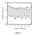
- FIG. 6 is a view showing variations in the resistance value when an experiment of unipolar switching operation was conducted on the variable resistive element used in the first embodiment, through the load resistor.
- FIG. 7 is a view showing variations in the resistance value when the experiment of unipolar switching operation was conducted on the variable resistive element used in the first embodiment, through load resistor.
- FIG. 8 is a block diagram schematically showing relations among the variable resistive element of the selected memory cell as a writing target, the load circuit, and the voltage switch circuit in the first embodiment.
- FIG. 9 is a circuit diagram schematically showing connection relations of a memory cell array, a word line decoder, a bit line decoder, and a load resistive characteristic variable circuit in the first embodiment.
- FIGS. 10A to 10D are circuit diagrams showing circuit configuration examples of the load resistive characteristic variable circuit shown in FIG. 9 .
- FIGS. 11A to 11E are circuit diagrams showing other circuit configuration examples of the load resistive characteristic variable circuit.
- FIG. 12 is a block diagram showing a schematic example of circuit configuration in the second embodiment of the nonvolatile semiconductor memory device according to the present invention.
- FIGS. 13A and 13B are a schematic vertical sectional view and an equivalent circuit diagram showing one example of configuration of a 1T1R type memory cell in the second embodiment.
- FIG. 14 is a circuit diagram showing a partial configuration of a memory cell array using the 1T1R type memory cell shown in FIG. 13 .
- FIG. 15 is a circuit diagram schematically showing connection relations among a memory cell array, a word line decoder, a bit line decoder, and a load resistive characteristic variable circuit in the second embodiment.
- FIG. 16 is a block diagram showing a schematic example of circuit configuration in a third embodiment of the nonvolatile semiconductor memory device according to the present invention.
- FIG. 17 is a circuit diagram showing a partial configuration of a cross point memory cell array shown in FIG. 16 .
- FIG. 18 is a block diagram showing a schematic example of circuit configuration in a fourth embodiment of the nonvolatile semiconductor memory device according to the present invention.
- FIG. 19 is a circuit diagram schematically showing connection relations among a memory cell array, a word line decoder, a bit line decoder, and a load resistive characteristic variable circuit in the fourth embodiment.
- FIG. 20 is a circuit diagram showing a circuit configuration example of a bit line driver shown in FIG. 19 .
- FIG. 21 is a block diagram showing a schematic example of circuit configuration in a fifth embodiment of the nonvolatile semiconductor memory device according to the present invention.
- FIG. 22 is a block diagram showing a schematic example of circuit configuration in another embodiment of the nonvolatile semiconductor memory device according to the present invention.
- FIG. 23 is a current-voltage characteristic diagram showing the resistive characteristics of the conventional variable resistive element capable of bipolar switching operations measured without going through the load resistance.
- FIG. 24 is a current-voltage characteristic diagram showing the resistive characteristics of the conventional variable resistive element capable of bipolar switching operations measured through the load resistance.
- FIGS. 25A and 25B are two types of current-voltage characteristic diagrams showing the resistive characteristics of the conventional variable resistive element capable of unipolar switching operations measured through the load resistance.
- FIGS. 26A and 26B are two types of current-voltage characteristic diagrams showing the resistive characteristics of the variable resistive element capable of unipolar switching operations based on the present invention measured through the load resistance.
- FIG. 27 is a current-voltage characteristic diagram showing the resistive characteristics of the variable resistive element capable of bipolar switching operations based on the present invention measured through the load resistance.
- FIG. 1 shows a block configuration of a device of the present invention 10 according to one embodiment.
- the device of the present invention 10 comprises a memory cell array 11 , a word line decoder (corresponding to a word line selection circuit) 12 , a bit line decoder (corresponding to a bit line selection circuit) 13 , a load resistance characteristic variable circuit 14 , a readout circuit 15 , a control circuit 16 , and a voltage switch circuit 17 .
- the memory cell array 11 comprises a plurality of arrays of nonvolatile memory cells arranged in a row direction and in a column direction, respectively, and not only information can be electrically programmed into memory cells to be addressed from the external, but also information stored in the addressed memory cells can be read out. More specifically, information is stored in specific memory cells in the memory cell array 11 that correspond to an address signal entered from an address line 18 , and the information is outputted to an external device through a data line 19 .
- a first writing operation (hereinafter referred to as a reset operation) in which the resistive characteristics of a variable resistive element in the memory cell transit from a low resistance state to a high resistance state
- a second writing operation (hereinafter referred to as a set operation) in which the resistive characteristics of the variable resistive element transit from the high resistance state to the low resistance state is performed with respect to each memory cell as a writing target so as to be assigned based on data to be programmed. For example, data “0” is programmed in the reset operation, and data “1” is programmed in the set operation to the memory cell as the writing target at the same time.
- the word line decoder 12 selects, as a selected word line, a word line of the memory cell array 11 that corresponds to an address signal entered in the address line 18 for row selection, and individually applies to the selected word line and an unselected word line selected word line voltage and unselected word line voltage for respective memory operations such as set, reset, and readout.
- the bit line decoder 13 selects, as a selected bit line, a bit line of the memory cell array 11 that corresponds to an address array that corresponds to an address signal entered the address line 18 for column selection, and individually applies to the selected bit line and an unselected bit line selected bit line voltage and unselected bit line voltage for respective memory operations.
- the load resistive characteristic variable circuit 14 is included in a load circuit that electrically connects to a selected memory cell in series that was selected from the memory cell array 11 as a target of writing by the word line decoder 12 and bit line decoder 13 in writing operation (set, reset or both), and controlled by a control circuit 16 so as to switch the load resistive characteristics specified by the current-voltage characteristics of the load circuit between two different load resistive characteristics (low resistance state and high resistance state).
- the load resistive characteristic variable circuit 14 is provided between the bit line decoder 13 and the memory cell array 11 for every bit line.
- the control circuit 16 controls the respective memory operations of set, reset and read out of the memory cell array 11 . Based on an address signal entered from the address line 18 , data entry made from the data line 19 (in writing operation), and a control input signal entered from a control signal line 20 , the control circuit 16 controls the word line decoder 12 and bit line decoder 13 to control readout, set and reset operations in the memory cell array 11 . Specifically, in each memory operation, the control circuit executes control for applying to each of the selected word line, unselected word line, selected bit line and unselected bit line, predetermined voltage corresponding to the respective memory operations, on the voltage switch circuit 17 , the word line decoder 12 , bit line decoder 13 or the like.
- control circuit 16 In particular, in writing operation, it controls voltage amplitude and pulse width of each voltage pulse to be applied to a memory cell to be written through the load circuit (including the load resistive characteristic variable circuit 14 ). Furthermore, in writing operation, it executes control for switching the load resistive characteristics of the load circuit on the load resistive characteristic variable circuit 14 .
- the control circuit 16 is provided with the capability in general as an address buffer circuit, a data input/output buffer circuit, a control input buffer circuit (not shown).
- the voltage switch circuit 17 provides the word line decoder 12 and the bit line decoder 13 with selected word line voltage, unselected word line voltage, selected bit line voltage and unselected bit line voltage necessary for readout and writing operations of the memory cell array 11 .
- Vcc represents service voltage (supply voltage) of the device of the present invention 10
- Vss represents ground voltage
- Vwr represents writing voltage for set and reset operations
- Vrd represents voltage for readout.
- selected bit line voltage in writing operation is supplied to the selected bit line through the load resistive characteristic variable circuit 14 .
- Data readout is performed from the memory cell array 11 through the bit line decoder 13 and a readout circuit 15 .
- the readout decoder 15 judges status of data, sends result thereof to the control circuit 16 , and outputs it to the data line 19 .
- FIG. 2 schematically shows partial configuration of the cross-point type memory cell array 11 .
- memory cells M are held at intersections of four bit lines BL 0 to BL 3 and four word lines WL 0 to WL 3 .
- the memory cell array 11 has the cross-point type memory cell array structure, wherein a plurality of memory cells M of two-terminal structure having variable resistive elements that store information as a result changes in electrical resistance are arranged in a row direction and in a column direction, respectively.
- It comprises a plurality of word lines extending in the row direction and a plurality of bit lines extending in the column direction, wherein each of the memory cells in the same row has one end of the memory cell connected to a common word line, and each of the memory cells in the same column has the other end of the memory cell connected to a common bit line.
- the memory cell M is a 1D1R type memory cell including a serial circuit in which a variable resistive element 21 having a three-layer structure including a lower electrode 23 , a variable resistor 24 , and an upper electrode 25 , and a diode 22 configured by a PN junction of a P-type semiconductor layer 26 and an N-type semiconductor layer 27 are connected vertically.
- the variable resistor 24 can be formed of an oxide or oxynitride containing a transition metal (Ti, Cu, Co, Ni, V, W, Fe and the like) such as TiO x N y and Fe 2 O 3 .
- the P-type semiconductor layer 26 and the N-type semiconductor layer 27 are formed by injecting P-type and N-type impurities to silicon, respectively.
- the variable resistor 24 is formed of TiO x N y produced by oxidizing TiN, the lower electrode 23 is formed of Ti or TiN, and the upper electrode 25 is formed of TiN.
- variable resistive element 21 may be fabricated on a predetermined substrate of semiconductor or insulator by using thin-film forming methods such as sputtering or the like, and photolithography technology or etching technology. Details of fabrication methods are omitted herein.
- One of the P-type semiconductor layer 26 and the upper electrode 25 serving as the two terminals of the memory cell M is connected to the word line, and the other of them is connected to the bit line.
- a lower wiring 28 is connected to the lower side of the P-type semiconductor layer 26
- an upper wiring 29 is connected to the upper side of the upper electrode 25 , and they are arranged orthogonally.
- the lower wiring 28 and the upper wiring 29 are formed of different materials or have different structures from the lower electrode 23 and the upper electrode 25 to reduce wiring resistance
- the lower wiring 28 is formed of AlCu or has a laminated layer structure of AlCu and TiN, for example
- the upper wiring 29 has a laminated structure of AlCu and TiN, for example.
- the lower wiring 28 since a positive writing voltage pulse is applied from the bit line side to the selected memory cell, the lower wiring 28 extends in a column direction to form the bit line, and the upper wiring 29 extends in a row direction to form the word line.
- the upper electrode 24 may extend in the row direction to form the word line without providing the upper wiring 29 .
- the lower wiring 28 becomes the word line and the upper wiring 29 becomes the bit line that is, when the lower wiring 28 and the upper wiring 29 are exchanged, it is necessary to apply a negative writing voltage pulse to the bit line or to reverse the PN junction by exchanging the P-type semiconductor layer 26 and the N-type semiconductor layer 27 of the diode 22 .
- the variable resistive element 21 having the structure as shown in FIG. 3 has two resistive characteristics of high resistance state (characteristics A) and low resistance state (characteristics B), for instance, as shown in FIG. 4 .
- the resistive characteristics of the variable resistive element can transit in both directions by applying voltage of same polarity between the two resistive characteristics. According to the present embodiment, when the element structure of the variable resistive element is asymmetric in a vertical direction, it is equivalent to the case where the positive or negative voltage polarity of the resistive characteristics shown in FIG. 23 is used.
- variable resistive element when the structure of the variable resistive element is symmetric in the vertical direction (when the materials of the upper electrode and the lower electrode and geometric dimensions thereof are the same), the two resistive characteristics A and B are symmetric to polarities of the applied voltages, respectively.
- positive and negative of the voltage polarities may be specified by positive and negative polarities of voltage to be applied to the lower electrode 23 relative to the upper electrode 24 .
- the resistive characteristics of the high resistance state (characteristics A) and the low resistance state (characteristics B) shown in FIG. 4
- the resistive characteristics transit from the high resistance state to the low resistance state by applying a voltage equal to or higher than a second threshold voltage Va that is a lower limit value of the absolute value of the applied voltage required for the resistive characteristics to transit from the high resistance state to the low resistance state, and setting a current compliance to be lower than a current value Ib provided when a first threshold voltage Vb, that is a lower limit value of the absolute value of the applied voltage required for the resistive characteristics to transit from the low resistance state to the high resistance state, is applied in the low resistance state, while in the low resistance state, the resistive characteristics transit from the low resistance state to the high resistance state by setting the current compliance to be higher than the current value Ib, and applying a voltage that is equal to or higher than the first threshold voltage Vb but lower than the second threshold voltage Va.
- the switching operation between the high resistance state (characteristics A) and the low resistance state (characteristics B) can be implemented by switching the setting of the current compliance.
- the resistive characteristics do not transit from the low resistance state to the high resistance state stably.
- the switching of the setting of the current compliance is equivalently implemented by changing the load resistive characteristics in the load resistive characteristic variable circuit 14 .
- the load circuit connecting in series with the variable resistive element that is a memory cell in the writing operation is assumed to be the word line decoder 12 , the bit line decoder 13 , the load resistive characteristic variable circuit 14 and a synthetic circuit such as parasitic resistance of signal wiring that connects these circuits.
- the description assumes stand-alone load resistance having linear load resistive characteristics.
- FIG. 5A is the I-V characteristic curve showing two resistive characteristics of high resistance state (characteristics A) and low resistance state (characteristics B) of a variable resistive element when it is measured without going through load resistance.
- a transition from the high resistance state to the low resistance state occurs at a transition point Ta (Va, Ia).
- a transition from the low resistance state to the high resistance state occurs at a transition point Tb (Vb, Ib).
- voltage Va corresponds to the second threshold voltage
- voltage Vb corresponds to the first threshold voltage
- current Ia corresponds to the second threshold current
- current Ib is referred to as the first threshold current.
- the load resistive characteristic line C 1 In order to perform stable operation from the high resistance state to the low resistance state, it is required that the load resistive characteristic line C 1 intersect the I-V characteristic curve in the low resistance state at a point T 1 (Vt 1 , It 1 ) on the low voltage side of the transition point Tb (Vb, Ib) from the low resistance state to the high resistance state.
- Equation (1) Va ⁇ Vb )/( Ib ⁇ Ia ) ⁇ R 1 (2)
- the resistance value in the left term of the Equation (2) is defined as the critical resistance value.
- the voltage amplitude Vda of voltage pulses that have the variable resistive element transit from the high resistance state to the low resistance state through load resistance should have higher voltage than the second critical voltage VA.
- the voltage amplitude Vda should satisfy the following Equation (4). Vda>Va+R 1 ⁇ Ia (4)
- the load resistive characteristic line C 2 intersects the I-V characteristic curve in the high resistance state at a point T 2 (Vt 2 , It 2 ) on the low voltage side of the transition point Ta (Va, Ia) from the high resistance state to the low resistance state.
- the resistance value in the left term of the Equation (6) is the same critical resistance value as the resistance value in the left term of the Equation (2).
- the voltage amplitude Vdb of voltage pulses that have the variable resistive element transit from the low resistance state to the high resistance state through load resistance should have higher voltage than the first critical voltage VB.
- the voltage amplitude Vdb should satisfy the following Equation (8). Vdb>Vb+R 2 ⁇ Ib (8)
- the second critical voltage VA and the first critical voltage VB are different, it is possible to set same voltage to voltage amplitude Vda of voltage pulses for having the variable resistive element from the high resistance state to the low resistance state and voltage amplitude Vdb for having the variable resistive element from the low resistance state to the high resistance state, as far as they satisfy the Equations (4) and (8).
- the voltage amplitude Vdb has considerably higher voltage than the first critical voltage VB, and in FIG. 5C , even if the load resistive characteristic line C 2 moves in parallel to the right (the high voltage direction) and the intersection between the load resistive characteristic line C 2 and the I-V characteristic curve in the high resistance state (characteristics A) moves to the high voltage side of the transition point Ta (Va, Ia), then bidirectional transitions occur between the high resistance state and the low resistance state, thus leading to unstable oscillation condition.
- the load resistive characteristic line C 2 moves in parallel to the left (direction of low voltage) as the voltage amplitude Vdb lowers, and the intersection between the load resistive characteristic line C 2 and the I-V characteristic curve in the high resistance state (characteristics A) moves to the low voltage side of the transition point Ta (Va, Ia).
- the voltage amplitude Vda has considerably higher voltage than the second critical voltage VA, and in FIG.
- FIGS. 6 and 7 show examples of the measurement results when the load resistive characteristics are switched stably by switching the set operation and reset operation repeatedly.
- FIG. 6 shows the switching characteristics when a voltage pulse having a voltage amplitude of 5 V is applied for 30 ns by use of a load resistance of 1.5 k ⁇ during the set operation, and a voltage pulse having a voltage amplitude of 3 V is applied for 30 ns without using the load resistance (load resistance is 0 ⁇ ) during the reset operation.
- FIG. 6 shows the switching characteristics when a voltage pulse having a voltage amplitude of 5 V is applied for 30 ns by use of a load resistance of 1.5 k ⁇ during the set operation, and a voltage pulse having a voltage amplitude of 3 V is applied for 30 ns without using the load resistance (load resistance is 0 ⁇ ) during the reset operation.
- FIG. 6 shows the switching characteristics when a voltage pulse having a voltage amplitude of 5 V is applied for 30 ns by use of a load resistance of 1.5 k ⁇ during the
- FIG. 7 shows the switching characteristics when a voltage pulse having a voltage amplitude of 5 V is applied for 30 ns by use of a load resistance of 1.5 k ⁇ during the set operation, and a voltage pulse having a voltage amplitude of 5 V is applied for 30 ns without using the load resistance (load resistance is 0 ⁇ ) during the reset operation.
- load resistance is 0 ⁇
- the voltage amplitude in the set operation is different from that in the reset operation in FIG. 6
- the set operation and the reset operation have the same voltage amplitude in FIG. 7 . In either case, the stable switching operation is confirmed.
- the load resistive characteristics are nonlinear in actual circuit configuration, as the load circuit includes transistors, that have nonlinear current-voltage characteristics for selecting a word line or a bit line, of the word line decoder 12 or the bit line decoder 13 . Even when the load resistive characteristics are nonlinear, the idea about the above principle operation and the method of determining optimal load resistive characteristics would be the same.
- FIG. 8 schematically shows a relation of the variable resistive element 21 of the selected memory cell to be written, the load circuit and the voltage switch circuit 17 .
- the load circuit can be treated as all circuits to which voltage pulses are applied from the voltage switch circuit 17 excluding the selected memory cell, and include the word line decoder 12 , the bit line decoder 13 , the load resistive characteristic variable circuit 14 , and parasitic resistance of signal wiring such as the selected word line or selected bit line or the like.
- the load resistive characteristics are assumed as the current-voltage characteristics of synthetic circuit of all circuits excluding the selected memory cell.
- the ground voltage Vss is applied from the voltage switch circuit 17 to one selected word line through the word line decoder 12 , and a voltage Vwr is applied as the writing voltage pulse to the plurality of selected bit lines through the bit line decoder 13 and the load resistive characteristic variable circuit 14 .
- the voltage Vwr is applied to the unselected word line through the word line decoder 12 , the same writing voltage pulse is applied to both ends of the unselected memory cell positioned between the unselected word line and the selected bit line at the same time, and the effective writing voltage is not applied thereto.
- the ground voltage Vss is applied to the unselected bit line through the bit line decoder 13 and the load resistive characteristic variable circuit 14 , and the ground voltage Vss is applied to both ends of the unselected memory cell positioned between the unselected bit line and the selected word line at the same time, and the effective writing voltage is not applied thereto.
- the writing voltage pulse is applied to both ends of the unselected memory cell positioned between the unselected bit line and the unselected word line so as to be biased reversely to the selected memory cell, the diode in the unselected memory cell becomes the reversely biased state, so that the reversely biased writing voltage pulse is not applied to the variable resistive element.
- FIG. 9 shows connection relations among the word line decoder 12 , the bit line decoder 13 and the load resistive characteristic variable circuit 14 to four bit lines BL 0 to 3 and four word lines WL 0 to 3 in the memory cell array 11 .
- the word line decoder 12 and the bit line decoder 13 only a last-stage word line driver 12 a and a bit line driver 13 a are shown, respectively and driven by row selecting signals RSB 0 to 3 and column selecting signal CS 0 , respectively.
- the four bit lines BL 0 to 3 are all selected or unselected at the same time, and the four bit lines correspond to bits of four-bit writing data D 0 to 3 . Therefore, the switching operations of the load resistive characteristics of the four load resistive characteristic variable circuits 14 are controlled by load resistance switching signals RLS 0 to 3 corresponding to the writing data D 0 to 3 , respectively.
- each of the word line driver 12 a and the bit line driver 13 a is provided with a buffer circuit having a level shifter (refer to FIG. 10C ), in which as a high potential during writing operation, not the power supply voltage Vcc but the write voltage pulse Vwr is supplied.
- the row selecting signals RSB 0 to 3 inputted to the word line drivers 12 a select the corresponding word lines WL 0 to 3 at low level but do not select them at high level.
- the column selection signal CS 0 inputted to the bit line driver 13 a selects the bit lines BL 0 to 3 at the same time at high level but does not select them at the same time at low level.
- FIG. 10A shows one example of a specific circuit configuration of the load resistive characteristic variable circuit 14 .
- the load resistive characteristic variable circuit 14 shown in FIG. 10A includes switch circuits 30 and 31 having two CMOS transfer gates, two high and low resistive elements RH (11 k ⁇ ) and RL (0.1 k ⁇ ) connected to the above circuits in series, respectively so that two serial circuits are connected in parallel, an inverter circuit 32 , and a buffer circuit 33 to generate complimentary input signals having the same voltage amplitude as that of the writing voltage Vwr inputted to the two switch circuits 30 and 31 , from the load resistance switching signals RLS 0 to 3 .
- switch circuits 30 and 31 having two CMOS transfer gates, two high and low resistive elements RH (11 k ⁇ ) and RL (0.1 k ⁇ ) connected to the above circuits in series, respectively so that two serial circuits are connected in parallel, an inverter circuit 32 , and a buffer circuit 33 to generate complimentary input signals having the same voltage amplitude as that of the writing
- the load resistive characteristics of the low resistance are to be used, while in the set operation (second writing operation) to transit the resistive characteristics of the variable resistive element from the high resistance state to the low resistance state, the load resistive characteristics of the high resistance are to be used.
- the signal level of the load resistance switching signals RLS 0 to 3 are set to high level, to turn on the switch circuit 30 and turn off the switch circuit 31 to select the side of the resistive element RL (0.1 k ⁇ )
- the signal level of the load resistance switching signals RLS 0 to 3 are set to low level, to turn on the switch circuit 31 and turn off the switch circuit 30 to select the side of the resistive element RL (1 k ⁇ ).
- FIGS. 10B and 10C show examples of the circuit configurations of the inverter circuit 32 and the buffer circuit 33 , respectively.
- the inverter circuit 32 and the buffer circuit 33 are provided with level shifter circuits as shown in FIGS. 10B and 10C .
- the inverter circuit 32 and the buffer circuit 33 are configured such that the normal inverter circuits are connected in two stages vertically.
- the circuit configuration of the buffer circuit 33 shown in FIG. 10C can be applied to the word line driver 12 a and the bit line driver 13 a.
- FIG. 10D shows an example of circuit configuration in which the load resistive characteristic variable circuit 14 shown in FIG. 10A is further simplified.
- FIGS. 11A to 11E show five examples of circuit configurations of the load resistive characteristic variable circuit 14 .
- FIG. 11A shows the load resistive characteristic variable circuit 14 configured by parallel connection of P-type MOSFET 34 a that is always in ON state and P-type MOSFET 34 b that can be switched ON and OFF by a control signal Sc 1 . If the P-type MOSFET 34 a and P-type MOSFET 34 b are set to the same size, switching of the nonlinear load resistive characteristics becomes possible by the control signal Sc 1 .
- resistive element having linear or nonlinear resistive characteristics or a diode adapted to voltage polarities could also implement the load resistance characteristic circuit 14 capable of switching the load resistive characteristics by turning the P-type MOSFET 34 b ON and OFF.
- FIG. 11B shows the load resistive characteristic variable circuit 14 configured by parallel connection of P-type MOSFETs 35 a , 35 b that can be switched ON or OFF by two control signals Sc 2 , Sc 3 .
- the P-type MOSFETs 35 a , 35 b are controlled so that one is turned ON while the other is turned OFF.
- switching of the nonlinear load resistive characteristics becomes possible by making a difference in gate width or the like of the P-type MOSFETs 35 a , 35 b .
- the P-type MOSFETs 35 a , 35 b may have the same size and resistance component of different resistance values may be added in series to both or any one of them.
- FIG. 11C shows the load resistive characteristic variable circuit 14 configured by one P-type MOSFET 36 that can control the gate voltage in multiple stages by one control signal Sc 4 . Switching of the nonlinear load resistive characteristics becomes possible, by configuring the control signal Sc 4 so that one signal level for turning OFF the P-type MOSFET 36 and two signal levels for turning ON the P-Type MOSFET 36 can be outputted, and by switching the two signal levels for turning ON the P-type MOSFET 36 .
- FIG. 11D shows the load resistive characteristic variable circuit 14 configured by one P-type MOSFET 37 that can control the gate voltage and back gate (substrate) voltage in two stages, respectively, with two control signals Sc 5 , Sc 6 .
- the control signal Sc 5 controls whether to turn ON or OFF the P-type MOSFET 37
- the control signal Sc 6 adjusts the back gate voltage of the P-type MOSFET 37 , thus changing the threshold voltage. Switching of the nonlinear load resistive characteristics becomes possible by turning ON the P-type MOSFET 37 and switching the threshold voltage in two ways to high or low, with the back gate voltage.
- FIG. 11E shows the load resistive characteristic variable circuit 14 configured by one resistive control element 38 that can control the gate voltage in multiple stages with one control signal Sc 7 .
- the resistive control element 38 a transfer gate composed of anything other than MOSFET or that composed of a single channel transistor or the like can be used. Switching of the load resistive characteristics becomes possible by switching signal levels of the control signal Sc 7 .
- control circuit 16 when the control circuit 16 is instructed by an address signal, a data entry signal, a control input signal, or the like from the external to write into a memory cell to be written specified by the address signal, it activates the voltage switch circuit 17 and gives instruction to output voltage to be applied to each of the selected word line, unselected word line, selected bit line, and unselected bit line, during writing operation.
- the voltage switch circuit 17 supplies the word line driver 12 a , the bit line driver 13 a , the inverter circuit 32 and the buffer circuit 33 with the writing voltage Vwr generated in a voltage generation circuit (not shown), and supplies the word line decoder 12 and the bit line decoder 13 with the ground voltage Vss.
- the ground voltage Vss and the writing voltage Vwr are applied to the selected word line and the unselected word line, respectively, and the writing voltage Vwr and the ground voltage Vss are supplied to the selected bit line and the unselected bit line through the load resistive characteristic variable circuit 14 , respectively. Therefore, the forward biased writing voltage Vwr is only applied to the selected memory cell connected between the plurality of selected bit lines and the one selected word line, and the voltage is not applied to the other unselected memory cells or reversely biased writing voltage Vwr is applied thereto. Thus, neither the set operation nor the reset operation is performed in the unselected memory cell.
- control circuit 16 controls the load resistive characteristic variable circuit 14 connected to each selected bit line connected to the selected memory cell as the writing target by a load resistance switching signal RLSi (i corresponds to each bit of the programming data) so as to implement the load resistive characteristics for the reset operation or the set operation corresponding to the writing data “0” or “1” of the selected memory cell. More specifically, in the load resistive characteristic variable circuit 14 , when the programming data is “0”, the load resistive characteristics on the low resistance side are selected, and when the programming data is “1”, the load resistive characteristics on the high resistance side are selected.
- the writing voltage Vwr is set such that the absolute value is to be equal to or higher than the first critical voltage VB mentioned above, and higher than the second critical voltage VA, the reset operation for the memory cell whose programming data is “0” and the set operation for the memory cell whose programming data is “1” are performed at the same time.
- the voltage fluctuation applied to the load circuit before and after the reset operation is controlled to be small, so that the voltage applied to both ends of the variable resistive element after the reset operation can be controlled to be equal to or lower than the second threshold voltage (Va) and the reset operation can be completed stably.
- the voltage fluctuation applied to the load circuit before and after the set operation is larger than that before and after the reset operation, so that the voltage applied to both ends of the variable resistive element after the set operation can be controlled to be equal to or lower than the first threshold voltage (Vb) and the set operation can be completed stably.
- a known readout operation for memory cells written through the conventional unipolar switching operation or bipolar switching operations may be used as readout operations of memory cells of the device of the present invention.
- the writing operations in which the set operation and reset operation are mixed can be performed for the plurality of memory cells at the same time by the unipolar switching operation in which the load resistive characteristics of the load circuit are switched between the set operation and the reset operation and the application time of the writing voltage Vwr is set to be equal.
- the memory cell is not limited to the 1D1R type, and even when the memory cell is a 1T1R type memory cell configured by the variable resistive element and a transistor for selecting the memory cell (MOSFET and the like), similarly, the writing operations in which the set operation and reset operation are mixed can be performed for the plurality of memory cells at the same time by the unipolar switching operation in which the load resistive characteristics of the load circuit are switched between the set operation and the reset operation and the application time of the writing voltage Vwr is set to be equal.
- the second embodiment in which the 1T1R type memory cell is used with reference to the drawings. It should be noted that the same reference symbols are given to the same components as those in the first embodiment.
- a block configuration of a device 40 of the present invention in the second embodiment is substantially the same as the block configuration in the first embodiment shown in FIG. 1 , and differs from the first embodiment only by a memory cell array 41 and a word line decoder 42 .
- FIG. 13A shows a schematic sectional view of 1T1R memory cell.
- Memory cells comprising the memory cell 41 is formed as a serial circuit of a selection transistor 52 and a variable resistive element 51 , the selection transistor 52 consisting of a source region 56 and a drain region 57 formed on a semiconductor substrate and a gate electrode 58 formed on a gate oxide film, and the variable resistive element 51 having the three-layered structure composed by laminating a lower electrode 53 , a variable resistor 54 and an upper electrode 55 , by electrically connecting the drain region 57 of the selection transistor 52 and the lower electrode 53 of the variable resistive element 51 .
- FIG. 13B is an equivalent circuit diagram of 1T1R type memory cell of the cross sectional structure shown in FIG. 13A .
- the selection transistor 52 is the N-type MOSFET in the present embodiment, it may be a P-type MOSFET or a bipolar transistor.
- a base electrode is connected to the word line WL, one of an emitter region or a collector region is connected to the source line SL or the bit line, and the other of the emitter region or the collector region is connected to one end of the variable resistive element 51 .
- FIG. 14 schematically shows partial configuration of the memory cell array 41 in which 1T1R type memory cells are arranged like a matrix.
- a gate of a selection transistor of each memory cell is connected to the word line (WL 0 to WLn ⁇ 1 )
- a source of the selection transistor of each memory cell is connected to the common source line SL
- one end (on the side of upper electrode) of the variable resistive element of each memory cell is connected to the bit line (BL 0 to BLm ⁇ 1 ).
- ground voltage is applied to the source line in respective memory operations of set, reset, and readout.
- the word line decoder 42 connects to each word line of the memory cell array 41 , and selects, as a selected word a word line of the memory cell array 41 corresponding to an address signal for row selection entered into the address line 18 . It individually applies to the selected word line and an unselected word line selected word line voltage and unselected word line voltage for respective memory operations of set, reset, and readout. Then, it turns on the selected transistor of the memory cell connecting to the selected word line, and turns off the selected transistor of the memory cell connecting to the unselected word line. Since the selected word line voltage during the writing operation only has to turn on the selection transistor of the selected memory cell, and does not necessarily have the same voltage as the writing voltage Vwr, the selected word line may be driven by the power supply voltage Vcc.
- FIG. 15 shows connection relations among the word line decoder 42 , the bit line decoder 13 and the load resistive characteristic variable circuit 14 to four bit lines BL 0 to 3 and four word lines WL 0 to 3 in the memory cell array 41 .
- the word line decoder 42 and the bit line decoder 13 only a last-stage word line driver 42 a and a bit line driver 13 a are shown, respectively and driven by row selecting signals RSB 0 to 3 and column selecting signal CS 0 , respectively.
- the four bit lines BL 0 to 3 are all selected or unselected at the same time, and the four bit lines correspond to bits of four-bit writing data D 0 to 3 . Therefore, the switching operations of the load resistive characteristics of the four load resistive characteristic variable circuits 14 are controlled by load resistance switching signals RLS 0 to 3 corresponding to the writing data D 0 to 3 , respectively.
- the word line driver 42 a is provided with a normal inverter circuit.
- the bit line driver 13 a is provided with a buffer circuit having a level shifter (refer to FIG. 10C ), in which as a high potential during writing operation, not the power supply voltage Vcc but the write voltage pulse Vwr is supplied.
- the row selecting signals RSB 0 to 3 inputted to the word line drivers 42 a select the corresponding word lines WL 0 to 3 at low level but do not select them at high level.
- the column selection signal CS 0 inputted to the bit line driver 13 a selects the bit lines BL 0 to 3 at the same time at high level but does not select them at the same time at low level.
- the load resistive characteristic variable circuit 14 may have the circuit configuration shown in FIGS. 10A and 10D or FIGS. 11A to 11E similar to the first embodiment.
- the bit line decoder 13 Since the bit line decoder 13 , the readout circuit 15 , the control circuit 16 , and the voltage switch circuit 17 are the same as those in the first embodiment, the overlapping description will not be given.
- the writing operations for the plurality of memory cells in the device 40 of the present invention in which the set operation and reset operation are mixed, since only the voltages applied to the selected word line and the unselected word line determined by the word line decoder 42 are different from those in the first embodiment, the overlapping description will not be given.
- the writing operations in which the set operation and reset operation are mixed can be performed for the plurality of memory cells at the same time by the unipolar switching operation in which the load resistive characteristics of the load circuit are switched between the set operation and the reset operation and the application time of the writing voltage Vwr is set to be equal.
- the memory cell is not limited to the 1D1R type, even when the memory cell is a 1R type memory cell configured only by the variable resistive element, similarly, the writing operations in which the set operation and reset operation are mixed can be performed for the plurality of memory cells at the same time by the unipolar switching operation in which the load resistive characteristics of the load circuit are switched between the set operation and the reset operation and the application time of the writing voltage Vwr is set to be equal.
- the third embodiment in which the 1R type memory cell is used with reference to the drawings. It should be noted that the same reference symbols are given to the same components as those in the first embodiment.
- a block configuration of a device 60 of the present invention in the third embodiment is substantially the same as the block configuration in the first embodiment shown in FIG. 1 , and differs from the first embodiment only by a memory cell array 61 and a voltage switch circuit 67 .
- FIG. 17 is a schematic view showing a partial configuration of a cross point memory cell array 61 .
- memory cells M are arranged at points where four bit lines BL 0 to 3 and four word lines WL 0 to 3 cross.
- the memory cell array 61 has a cross point memory cell array structure in which a plurality of two-terminal structured memory cells M each having the variable resistive element to store information according to the change of the electric resistance are arranged in a row direction and a column direction.
- the memory cell array 61 includes a plurality of word lines extending in the row direction and a plurality of bit lines extending in the column direction, where each of the memory cells in the same row has one end of the memory cell connected to a common word line, and each of the memory cells in the same column has the other end of the memory cell connected to a common bit line.
- the memory cell M is configured only by the variable resistive element 21 used in the memory cell according to the first embodiment. Therefore, the resistive characteristics of the variable resistive element 21 are the same as in the first embodiment, and as shown in FIG. 4 , the resistive characteristics take the high resistance state (characteristics A) and the low resistance state (characteristics B) and can transit between the two resistive characteristics bi-directionally in response to the application of the voltage having the same polarity.
- the voltage switch circuit 67 applies a selected word line voltage, an unselected word line voltage, a selected bit line voltage, and an unselected bit line voltage necessary in the reading operation and writing operation in the memory cell array 61 , to the word line decoder 12 and the bit line decoder 13 .
- Vcc represents a supply voltage (power supply voltage) of the device 10 of the present invention
- Vss represents the ground voltage
- Vwr represents a writing voltage for both set operation and reset operation
- Vrd represents a reading voltage
- Vpr represents a writing preventing voltage.
- the selected bit line voltage during writing operation is supplied to the selected bit line through the bit line decoder 13 and the load resistive characteristic variable circuit 14 .
- the writing preventing voltage Vpr is applied to the unselected bit line through the bit line decoder 13 and applied to the unselected word line through the word line decoder 12 .
- the ground voltage Vss is applied to the unselected bit line and the writing voltage Vwr is applied to the unselected word line in the first embodiment
- the writing preventing voltage Vpr that is intermediate in level between the writing voltage Vwr and the ground voltage Vss is applied to the unselected bit line and the unselected word line in order to prevent the set operation and the reset operation in the unselected memory cell with respect to either of the positive and negative voltage polarities.
- the writing voltage Vwr is applied to the plurality of selected bit lines through the load resistive characteristic variable circuit 14 similar to the first embodiment, and the ground voltage Vss is applied to the one selected word line similar to the first embodiment.
- the writing preventing voltage Vpr or a voltage calculated by subtracting the writing preventing voltage Vpr from the writing voltage Vwr (Vwr ⁇ Vpr) is applied to both ends of the unselected memory cell connected between the unselected bit line and the selected word line, and the unselected memory cell connected between the selected bit line and the unselected word line
- both writing preventing voltage Vpr and the difference voltage (Vwr ⁇ Vpr) are equal to or lower than the first threshold voltage with respect to either the positive or negative polarities of the applied voltage
- the absolute value of the first threshold voltage is smaller than the absolute value of the second threshold voltage.
- the set operation and the reset operation can be prevented with respect to either the positive or negative applied voltage polarities.
- both ends of the unselected memory cell connected between the unselected bit line and the unselected word line are at the same voltage, the voltage is not applied thereto, so that the set operation and the reset operation are prevented.
- the word line decoder 12 Since the word line decoder 12 , the bit line decoder 13 , the readout circuit 15 , and the control circuit 16 are the same as those in the first embodiment, the overlapping description will not be given.
- the writing operations for the plurality of memory cells in the device 60 of the present invention in which the set operation and reset operation are mixed since only the voltages applied to the unselected bit line and the unselected word line differ from the first embodiment, the overlapping description will not be given.
- the memory cell is the 1D1R type memory cell similar to the first embodiment.
- the fourth embodiment using the 1D1R type memory cell will be described with reference to the drawing. It should be noted that the same reference symbols are given to the same components as those in the first embodiment.
- the voltage amplitude Vwr 1 of the set voltage pulse is set to be higher than the second critical voltage VA
- the voltage amplitude Vwr 2 of the reset voltage pulse is set to be higher than the first critical voltage VB but lower than the second critical voltage VA. That is, the voltage amplitude Vwr 1 of the set voltage pulse is higher than the voltage amplitude Vwr 2 of the reset voltage pulse (Vwr 1 >Vwr 2 ).
- the first critical voltage VB and the second critical voltage VA have been described in the first embodiment, the overlapping description will not be given.
- a block configuration of a device 80 of the present invention in the fourth embodiment is substantially the same as the block configuration shown in FIG. 1 in the first embodiment, and differs from the first embodiment only by a bit line driver 83 a of a bit line decoder 83 and a voltage switch circuit 87 .
- FIG. 19 shows connection relations among the word line decoder 12 , the bit line decoder 83 and the load resistive characteristic variable circuit 14 to four bit lines BL 0 to 3 and four word lines WL 0 to 3 in the memory cell array 11 .
- the word line decoder 12 and the bit line decoder 83 only a last-stage word line driver 12 a and a bit line driver 83 a are shown, respectively and driven by row selecting signals RSB 0 to 3 and column selecting signal CS 0 , respectively.
- the four bit lines BL 0 to 3 are all selected or unselected at the same time, and the four bit lines correspond to bits of four-bit writing data D 0 to 3 . Therefore, the switching operations of the load resistive characteristics of the four load resistive characteristic variable circuits 14 are controlled by load resistance switching signals RLS 0 to 3 corresponding to the writing data D 0 to 3 , respectively.
- the word line driver 12 a is provided with a buffer circuit having a level shifter (refer to FIG. 10C ), in which as a high potential during writing operation, not the power supply voltage Vcc but the set voltage pulse Vwr 1 (>Vwr 2 ) is supplied.
- the row selecting signals RSB 0 to 3 inputted to the word line drivers 12 a select the corresponding word lines WL 0 to 3 at low level but do not select them at high level.
- the bit line driver 83 a is a buffer circuit provided with a level shifter, in which the high potential during writing operation can be individually selected by load resistance switching signals RLS 0 to 3 between the voltage amplitude Vwr 1 of the set voltage and the voltage amplitude Vwr 2 of the reset voltage.
- a column selecting signal CS 0 inputted to the bit line driver 83 a selects the bit lines BL 0 to 3 at high level at the same time and does not select them at low level at the same time.
- An inverter circuit 88 and a buffer circuit 89 to receive the load resistance switching signal RLS 0 to 3 are each provided with a level shifter, and the circuit configurations thereof are the same as the inverter circuit 32 and the buffer circuit 33 shown in FIGS. 10B and 10C .
- the inverter circuit 88 becomes unselected state when the load resistance switching signals RLS 0 to 3 are at low level and outputs the voltage Vwr 2 , and becomes selected state when the load resistance switching signals RLS 0 to 3 are at high level and outputs the ground voltage Vss (0 V).
- the buffer circuit 89 becomes unselected state when the load resistance switching signals RLS 0 to 3 are at high level and outputs the voltage Vwr 1 , and becomes selected state when the load resistance switching signals RLS 0 to 3 are at low level and outputs the ground voltage Vss (0 V).
- the load resistive characteristic variable circuit 14 may have the circuit configuration shown in FIGS. 10A and 10D or FIGS. 11A to 11E similar to the first embodiment.
- control circuit 16 when the control circuit 16 is instructed by an address signal, a data entry signal, a control input signal, or the like from the external to write into a memory cell to be written specified by the address signal, it activates the voltage switch circuit 87 and gives instruction to output voltage to be applied to each of the selected word line, unselected word line, selected bit line, and unselected bit line, during writing operation.
- the voltage switch circuit 87 supplies the bit line driver 83 a , the inverter circuit 88 and the buffer circuit 89 with the writing voltages Vwr 1 and Vwr 2 generated in a voltage generation circuit (not shown), supplies the word line driver 12 a with the writing voltage Vwr 1 , and supplies the word line decoder 12 and the bit line decoder 83 with the ground voltage Vss.
- the ground voltage Vss and the writing voltage Vwr 1 are applied to the selected word line and the unselected word line, respectively.
- the writing voltage Vwr 1 or Vwr 2 is supplied to the selected bit line through the load resistive characteristic variable circuit 14 , and the ground voltage Vss is applied to the unselected bit line through the load resistive characteristic variable circuit 14 .
- the forward biased writing voltage Vwr 1 or Vwr 2 is only applied to the selected memory cells connected between the plurality of selected bit lines and the one selected word line, and the voltage is not applied to the other unselected memory cells or reversely biased writing voltage Vwr 1 or the difference between the two writing voltages Vwr 1 and Vwr 2 (Vwr 1 -Vwr 2 ) is applied thereto. Thus, neither the set operation nor the reset operation is performed in the unselected memory cell.
- control circuit 16 controls the load resistive characteristic variable circuit 14 connected to each selected bit line connected to the selected memory cell as the writing target by a load resistance switching signal RLSi (i corresponds to each bit of the programming data) so as to implement the load resistive characteristics for the reset operation or the set operation corresponding to the writing data “0” or “1” of the selected memory cell. More specifically, in the load resistive characteristic variable circuit 14 , when the programming data is “0”, the load resistive characteristics on the low resistance side are selected, and when the programming data is “1”, the load resistive characteristics on the high resistance side are selected.
- control circuit 16 individually controls the high potential level outputted from the bit line driver 83 a connected to the load resistive characteristic variable circuit 14 corresponding to the respective selected memory cell as the writing target to be the reset voltage Vwr 2 or the set voltage Vwr 1 based on the programming data “0” or “1” of the selected memory cell, by the load resistance switching signal RLSi (i corresponds to each bit of the programming data).
- the pulse widths of the set voltage pulse Vwr 1 and the reset voltage pulse Vwr 2 outputted from the bit line driver 83 a are controlled by the control circuit 16 to be the same pulse width (application time).
- control circuit 16 controls the load resistive characteristic variable circuit 14 and the bit line driver 83 a , so that the absolute value of the reset voltage Vwr 2 is set to be equal to or higher than the first critical voltage VB, and the absolute value of the set voltage Vwr 1 is set to be equal to or higher than the second critical voltage VA, and the reset operation for the memory cell of the programming data “0” and the set operation for the memory cell of the programming data “1” are executed at the same time.
- the voltage fluctuation applied to the load circuit before and after the reset operation is controlled to be small, so that the voltage applied to both ends of the variable resistive element after the reset operation can be controlled to be equal to or lower than the second threshold voltage (Va) and the reset operation can be completed stably.
- the voltage fluctuation applied to the load circuit before and after the set operation is larger than that before and after the reset operation, so that the voltage applied to both ends of the variable resistive element after the set operation can be controlled to be equal to or lower than the first threshold voltage (Vb) and the set operation can be completed stably.
- the writing operations in which the set operation and reset operation are mixed can be performed for the plurality of memory cells at the same time by the unipolar switching operation in which the load resistive characteristics of the load circuit are switched between the set operation and the reset operation and the application time of the writing voltages Vwr 1 and Vwr 2 are set to be equal.
- the memory cell is not limited to the 1D1R type, even when the memory cell is a 1T1R type memory cell configured by the variable resistive element and a transistor for selecting the memory cell (MOSFET and the like), similarly, the writing operations in which the set operation and reset operation are mixed can be performed for the plurality of memory cells at the same time by the unipolar switching operation in which the load resistive characteristics of the load circuit are switched between the set operation and the reset operation and the application time of the writing voltages Vwr 1 and Vwr 2 are set to be equal to each other.
- the 1T1R type memory cell is used with reference to the drawings. It should be noted that the same reference symbols are given to the same components as those in the first embodiment and the second embodiment.
- a block configuration of a device 90 of the present invention in the fifth embodiment is substantially the same as the block configuration shown in FIG. 18 in the fourth embodiment or the block configuration shown in FIG. 12 in the second embodiment, and differs from the fourth embodiment only by the memory cell array 41 and the word line decoder 42 , and differs from the second embodiment by the bit line driver 83 a of the bit line decoder 83 and the voltage switch circuit 87 .
- the bit line driver 83 a of the bit line decoder 83 and the voltage switch circuit 87 are the same as those described in the fourth embodiment, the overlapping description will not be given.
- the readout circuit 15 and the control circuit 16 are the same as those described in the first embodiment, the overlapping description will not be given.
- the writing operations for the plurality of memory cells in the device 90 of the present invention in which the set operation and reset operation are mixed are the same as those in the fourth embodiment except that the applied voltages of the selected word line and the unselected word line determined by the word line decoder 42 are different, and the set operation and the reset operation for the selected memory cell are replaced with the selection transistor in which the forward biased diode is on in the selected memory cell, the overlapping description will not be given.
- the selection transistors are off in all of the unselected memory cells connected to the unselected word line, the writing voltages Vwr 1 and Vwr 2 are not applied to both ends of the variable resistive element, so that both the set operation and the reset operation are not performed.
- the unselected memory cells connected to the selected word line and the unselected bit line since the unselected bit line and the source line are at the ground voltage Vss, even when the selection transistor is on, the voltage is not applied to the variable resistive element, so that both the set operation and the reset operation are not performed.
- variable resistive element comprising memory cells
- Ti/TiON/TiN structure or TiN/TiON/TiN structure is adopted.
- the structure and material of the variable resistive element in each embodiment shall not be limited to the materials of the respective structures described above.
- variable resistive element when voltage is applied to the other terminal relative to one terminal with at least one of positive and negative polarities, the resistive characteristics specified by the current-voltage characteristics between two terminals can transmit between two resistive characteristics of low resistance state and high resistance state that can be taken stably, and if the variable resistive element has a first threshold voltage being the lower limit of an absolute value of applied voltage necessary for said resistive characteristics to transit from the low resistance state to the high resistance state and a second threshold voltage being the lower limit of an absolute value of applied voltage necessary for said resistive characteristics to transit from the high resistance state to the low resistance state, in which the first threshold voltage is lower than the second threshold voltage, the present invention may be applicable to any material or structure.
- variable resistor of a variable resistive element to which the present invention can apply metal oxides, metal oxynitrides, or organic thin film, etc. may be applied.
- the variable resistive element using oxides or oxynitrides including transition metal, oxides or oxynitrides including elements to be selected from Mn, Fe, Ni, Co, Ti, Cu and V or the variable resistive element using perovskite-type oxides such as PCMO, etc. is a variable resistive element having a first threshold voltage that is lower than a second threshold voltage and capable of producing similar effect when used in the present invention, although voltage values of the first threshold voltage and the second threshold voltage differ for individual structure or every material.
- the diode 22 comprising the memory cells may be formed either on upper or lower side of the variable resistive element 21 .
- the diode 22 shall not be limited to the PN-junction type diode, and may be formed of Schottky barrier diodes. Otherwise, depending on polarity of applied voltage, forward direction of the diode 22 may be reversed to the direction shown in the above first and fourth embodiment.
- variable resistive element 51 is connected to the bit line, and the source region 56 of the selection transistor 52 is connected to the source line.
- the arrangement of the variable resistive element 51 and the selection transistor 52 may be exchanged so that the selection transistor is connected to the bit line, and the variable resistive element is connected to the source line.
- the load resistive characteristic variable circuit 14 is provided between the bit line decoder 13 , 83 and the memory cell array 11 , 41 with respect to each bit line.
- the arranged position of the load resistive characteristic variable circuit 14 is not limited to the position between the bit line decoder 13 , 83 and the memory cell array 11 , 41 , and it may not be arranged with respect to each bit line.
- the load resistive characteristic variable circuit 14 may be provided between the bit line decoder 13 and the voltage switch circuit 17 so as to be electrically connected to each of the plurality of selected bit lines selected by the bit line decoder 13 .
- the load resistive characteristics of the load circuit connected to each of the selected bit lines are set to either one of the two different load resistive characteristics by the load resistive characteristic variable circuit 14 , based on whether the programming data is “0” or “1”.
- the control for the load resistive characteristic variable circuit 14 is the same as that in the first embodiment, the overlapping description will not be given.
- the pulse width of the writing voltage pulse is the same between the set operation and the reset operation
- the pulse widths of the set operation and the reset operation may be different within a range of being 100 ns or less although it is not to be as different as the pulse widths in a conventional unipolar switching operation.
- the power consumption can be reduced during writing, and in addition, the high-speed writing as fast as 100 ns or less can be kept regardless of the set operation and the reset operation.
- the configuration of the cross point memory cell array is such that the plurality of word lines extend in the row direction, the bit lines extend in the column direction, the first ends of the plurality of memory cells arranged in the same row are connected to the common word line, and the second ends of the plurality of memory cells arranged in the same column are connected to the common bit line, in the case where the memory cell has the two-terminal structure, even when the word lines are replaced with the bit lines and the load resistive characteristic variable circuits are connected to the respective word lines, the same operation effect can be achieved as those in the above first, third, and fourth embodiments by replacing the word line decoder with the bit line decoder similarly.
- the set operation and the reset operation can be performed at the same time by the bipolar switching operation without using the negative voltage, by providing a pair of bit line and source line with respect to each column and switching the polarities of the writing voltage applied between the bit line and the source line between the set operation and the reset operation.
- the present invention can be used in a nonvolatile semiconductor memory device comprising a variable resistive element resistive characteristics of which change as result of voltage application, and, in particular, is effective in implementation of the nonvolatile semiconductor memory device capable of writing a plurality of memory cells at the same time by high-speed switching operations to the variable resistive element in a stable manner.
Abstract
Description
- Non-patent Document 1: H. Pagnia, et. al, “Bistable Switching in Electroformed Metal-Insulator-Metal Devices”, Physica Status Solidi (a), 108, pp. 11-65, 1988
- Non-patent Document 2: W. W. Zhuang, et. al, “Novell Colossal Magnetoresistive Thin Film Nonvolatile Resistance Random Access Memory (RRAM)”, IEDM Technical Digest, pp. 193-196, December 2002
- Non-patent Document 3: W. Y. Cho, et. al, “A 0.18 μm 3.0V 64 Mb Non-Volatile Phase-Transition Random-Access Memory (PRAM)”, 2004ISSCC Digest of Technical Papers, pp. 40-41, February 2004
V=−R1×(I−Ia)+Va (1)
(Va−Vb)/(Ib−Ia)<R1 (2)
R1=(Va−Vt1)/(It1−Ia) (3)
Vda>Va+R1×Ia (4)
V=−R2×(I−Ib)+Vb (5)
(Va−Vb)/(Ib−Ia)>R2 (6)
R2=(Vt2−Vb)/(Ib−It2) (7)
Vdb>Vb+R2×Ib (8)
Claims (11)
Applications Claiming Priority (3)
| Application Number | Priority Date | Filing Date | Title |
|---|---|---|---|
| JP2006330045A JP4088323B1 (en) | 2006-12-06 | 2006-12-06 | Nonvolatile semiconductor memory device |
| JP2006-330045 | 2006-12-06 | ||
| PCT/JP2007/071501 WO2008068991A1 (en) | 2006-12-06 | 2007-11-05 | Nonvolatile semiconductor storage device |
Publications (2)
| Publication Number | Publication Date |
|---|---|
| US20100080037A1 US20100080037A1 (en) | 2010-04-01 |
| US7952909B2 true US7952909B2 (en) | 2011-05-31 |
Family
ID=39491897
Family Applications (1)
| Application Number | Title | Priority Date | Filing Date |
|---|---|---|---|
| US12/517,025 Expired - Fee Related US7952909B2 (en) | 2006-12-06 | 2007-11-05 | Nonvolatile semiconductor memory device |
Country Status (5)
| Country | Link |
|---|---|
| US (1) | US7952909B2 (en) |
| JP (1) | JP4088323B1 (en) |
| CN (1) | CN101548334B (en) |
| TW (1) | TW200842875A (en) |
| WO (1) | WO2008068991A1 (en) |
Cited By (13)
| Publication number | Priority date | Publication date | Assignee | Title |
|---|---|---|---|---|
| US20100259967A1 (en) * | 2007-11-29 | 2010-10-14 | Sony Corporation | Memory cell |
| US20100315866A1 (en) * | 2009-06-15 | 2010-12-16 | Hynix Semiconductor Inc. | Phase change memory device having multi-level and method of driving the same |
| US20110267872A1 (en) * | 2008-05-07 | 2011-11-03 | Kabushiki Kaisha Toshiba | Resistance change memory device |
| US20120074507A1 (en) * | 2010-09-29 | 2012-03-29 | Crossbar, Inc. | Integration of an amorphous silicon resistive switching device |
| US20130170280A1 (en) * | 2011-12-28 | 2013-07-04 | Kabushiki Kaisha Toshiba | Semiconductor memory device |
| US20130272053A1 (en) * | 2012-04-12 | 2013-10-17 | Micron Technology, Inc. | Apparatuses and methods for providing set and reset voltages at the same time |
| US8654594B2 (en) * | 2012-02-23 | 2014-02-18 | International Business Machines Corporation | Vdiff max limiter in SRAMs for improved yield and power |
| US8692222B2 (en) | 2010-12-27 | 2014-04-08 | Panasonic Corporation | Nonvolatile memory element and method of manufacturing the nonvolatile memory element |
| US9378785B2 (en) | 2012-10-23 | 2016-06-28 | Industrial Technology Research Institute | Resistive random-access memory devices |
| US20160314835A1 (en) * | 2013-02-28 | 2016-10-27 | SK Hynix Inc. | Electronic device and method for operating electronic device |
| US9558813B2 (en) * | 2013-08-05 | 2017-01-31 | Jonker, Llc | Method of operating incrementally programmable non-volatile memory |
| US20180308546A1 (en) * | 2017-04-19 | 2018-10-25 | Winbond Electronics Corp. | Resistive random access memory device |
| US11152064B2 (en) | 2018-11-14 | 2021-10-19 | Samsung Electronics Co., Ltd. | Memory device, memory cell and method for programming memory cell |
Families Citing this family (25)
| Publication number | Priority date | Publication date | Assignee | Title |
|---|---|---|---|---|
| US7692999B2 (en) * | 2006-12-25 | 2010-04-06 | Semiconductor Energy Laboratory Co., Ltd | Nonvolatile memory and semiconductor device including nonvolatile memory |
| US8270199B2 (en) * | 2009-04-03 | 2012-09-18 | Sandisk 3D Llc | Cross point non-volatile memory cell |
| US8934293B1 (en) * | 2010-06-29 | 2015-01-13 | Contour Semiconductor, Inc. | Means and method for operating a resistive array |
| US8638084B1 (en) * | 2010-10-22 | 2014-01-28 | Xilinx, Inc. | Bandgap bias circuit compenastion using a current density range and resistive loads |
| JP5092006B2 (en) * | 2010-11-01 | 2012-12-05 | シャープ株式会社 | Nonvolatile semiconductor memory device and control method thereof |
| US8502185B2 (en) * | 2011-05-31 | 2013-08-06 | Crossbar, Inc. | Switching device having a non-linear element |
| US8331131B2 (en) | 2011-01-31 | 2012-12-11 | Hewlett-Packard Development Company, L.P. | Changing a memristor state |
| US10333064B2 (en) * | 2011-04-13 | 2019-06-25 | Micron Technology, Inc. | Vertical memory cell for high-density memory |
| JP5144843B2 (en) * | 2011-05-11 | 2013-02-13 | パナソニック株式会社 | Cross-point type variable resistance nonvolatile memory device and reading method thereof |
| JP5542742B2 (en) * | 2011-05-26 | 2014-07-09 | 株式会社東芝 | Semiconductor memory device |
| JP5671413B2 (en) * | 2011-06-07 | 2015-02-18 | ルネサスエレクトロニクス株式会社 | Nonvolatile semiconductor memory device and manufacturing method thereof |
| KR101929530B1 (en) * | 2012-02-21 | 2019-03-15 | 삼성전자주식회사 | Variable resistance memory device and driving method thereof |
| US8982647B2 (en) * | 2012-11-14 | 2015-03-17 | Crossbar, Inc. | Resistive random access memory equalization and sensing |
| US9373399B2 (en) * | 2013-07-22 | 2016-06-21 | Micron Technology, Inc. | Resistance variable element methods and apparatuses |
| US9178000B1 (en) * | 2014-04-29 | 2015-11-03 | Intermolecular, Inc. | Resistive random access memory cells having shared electrodes with transistor devices |
| US9343133B1 (en) * | 2014-10-27 | 2016-05-17 | Micron Technology, Inc. | Apparatuses and methods for setting a signal in variable resistance memory |
| CN105989877A (en) * | 2015-02-02 | 2016-10-05 | 华邦电子股份有限公司 | Resistance-type memory device |
| JP2016164938A (en) * | 2015-03-06 | 2016-09-08 | 株式会社日立製作所 | Phase change memory cell and memory array |
| CN106158013B (en) * | 2015-04-15 | 2019-03-05 | 华邦电子股份有限公司 | The method for writing data of resistance-type memory and its storage unit |
| WO2018063287A1 (en) * | 2016-09-30 | 2018-04-05 | Intel Corporation | Conductive bridge resistive random access memory cell |
| US10290327B2 (en) * | 2017-10-13 | 2019-05-14 | Nantero, Inc. | Devices and methods for accessing resistive change elements in resistive change element arrays |
| US10896726B2 (en) * | 2019-04-02 | 2021-01-19 | Junsung KIM | Method for reading a cross-point type memory array comprising a two-terminal switching material |
| JP2021039815A (en) * | 2019-09-05 | 2021-03-11 | キオクシア株式会社 | Semiconductor storage device |
| JP7150787B2 (en) | 2020-07-31 | 2022-10-11 | ウィンボンド エレクトロニクス コーポレーション | Resistance variable crossbar array device |
| JP2022139919A (en) * | 2021-03-12 | 2022-09-26 | キオクシア株式会社 | memory device |
Citations (5)
| Publication number | Priority date | Publication date | Assignee | Title |
|---|---|---|---|---|
| US6930909B2 (en) * | 2003-06-25 | 2005-08-16 | Micron Technology, Inc. | Memory device and methods of controlling resistance variation and resistance profile drift |
| US6937528B2 (en) * | 2002-03-05 | 2005-08-30 | Micron Technology, Inc. | Variable resistance memory and method for sensing same |
| US20060067106A1 (en) | 2004-09-30 | 2006-03-30 | Sony Corporation | Storage device and semiconductor device |
| JP2006190376A (en) | 2005-01-05 | 2006-07-20 | Sharp Corp | Nonvolatile semiconductor storage apparatus |
| JP2006203098A (en) | 2005-01-24 | 2006-08-03 | Sharp Corp | Non-volatile semiconductor storage device |
-
2006
- 2006-12-06 JP JP2006330045A patent/JP4088323B1/en not_active Expired - Fee Related
-
2007
- 2007-11-05 WO PCT/JP2007/071501 patent/WO2008068991A1/en active Application Filing
- 2007-11-05 US US12/517,025 patent/US7952909B2/en not_active Expired - Fee Related
- 2007-11-05 CN CN2007800450143A patent/CN101548334B/en not_active Expired - Fee Related
- 2007-11-20 TW TW096143981A patent/TW200842875A/en not_active IP Right Cessation
Patent Citations (7)
| Publication number | Priority date | Publication date | Assignee | Title |
|---|---|---|---|---|
| US6937528B2 (en) * | 2002-03-05 | 2005-08-30 | Micron Technology, Inc. | Variable resistance memory and method for sensing same |
| US6930909B2 (en) * | 2003-06-25 | 2005-08-16 | Micron Technology, Inc. | Memory device and methods of controlling resistance variation and resistance profile drift |
| US20060067106A1 (en) | 2004-09-30 | 2006-03-30 | Sony Corporation | Storage device and semiconductor device |
| JP2006099882A (en) | 2004-09-30 | 2006-04-13 | Sony Corp | Memory device and semiconductor device |
| JP2006190376A (en) | 2005-01-05 | 2006-07-20 | Sharp Corp | Nonvolatile semiconductor storage apparatus |
| JP2006203098A (en) | 2005-01-24 | 2006-08-03 | Sharp Corp | Non-volatile semiconductor storage device |
| US20090052225A1 (en) | 2005-01-24 | 2009-02-26 | Hidenori Morimoto | Nonvolatile Semiconductor Memory Device |
Non-Patent Citations (4)
| Title |
|---|
| H. Pagnia et al., "Bistable Switching in Electroformed Metal-Insulator-Metal Devices", Physica Status Solidi (a), 108, pp. 11-65, 1988. |
| W. W. Zhuang et al., "Novell Colossal Magnetoresistive Thin Film Nonvolatile Resistance Random Access Memory (RRAM)", IEDM Technical Digest, pp. 193-196, Dec. 2002. |
| W. Y. Cho et al., "A 0.18mum 3.0V 64Mb Non-Volatile Phase-Transition Random-Access Memory (PRAM)", 2004ISSCC Digest of Technical Papers, pp. 40-41, Feb. 2004. |
| W. Y. Cho et al., "A 0.18μm 3.0V 64Mb Non-Volatile Phase-Transition Random-Access Memory (PRAM)", 2004ISSCC Digest of Technical Papers, pp. 40-41, Feb. 2004. |
Cited By (32)
| Publication number | Priority date | Publication date | Assignee | Title |
|---|---|---|---|---|
| US20100259967A1 (en) * | 2007-11-29 | 2010-10-14 | Sony Corporation | Memory cell |
| US8295074B2 (en) * | 2007-11-29 | 2012-10-23 | Sony Corporation | Memory cell |
| US8897059B2 (en) * | 2008-05-07 | 2014-11-25 | Kabushiki Kaisha Toshiba | Resistance change memory device that stores a reversible resistance value as data |
| US20110267872A1 (en) * | 2008-05-07 | 2011-11-03 | Kabushiki Kaisha Toshiba | Resistance change memory device |
| US8842461B2 (en) * | 2009-06-15 | 2014-09-23 | SK Hynix Inc. | Phase change memory device having multi-level and method of driving the same |
| US20100315866A1 (en) * | 2009-06-15 | 2010-12-16 | Hynix Semiconductor Inc. | Phase change memory device having multi-level and method of driving the same |
| US20130094285A1 (en) * | 2009-06-15 | 2013-04-18 | SK Hynix Inc. | Phase change memory device having multi-level and method of driving the same |
| US8982605B2 (en) | 2009-06-15 | 2015-03-17 | SK Hynix Inc. | Phase change memory device having multi-level and method of driving the same |
| US8351240B2 (en) * | 2009-06-15 | 2013-01-08 | SK Hynix Inc. | Phase change memory device having multi-level and method of driving the same |
| US8982606B2 (en) | 2009-06-15 | 2015-03-17 | SK Hynix Inc. | Phase change memory device having multi-level and method of driving the same |
| US20150043268A1 (en) * | 2009-06-15 | 2015-02-12 | SK Hynix Inc. | Phase change memory device having multi-level and method of driving the same |
| US9087575B2 (en) * | 2009-06-15 | 2015-07-21 | SK Hynix Inc. | Phase change memory device having multi-level and method of driving the same |
| US20120074507A1 (en) * | 2010-09-29 | 2012-03-29 | Crossbar, Inc. | Integration of an amorphous silicon resistive switching device |
| US8723154B2 (en) * | 2010-09-29 | 2014-05-13 | Crossbar, Inc. | Integration of an amorphous silicon resistive switching device |
| US8692222B2 (en) | 2010-12-27 | 2014-04-08 | Panasonic Corporation | Nonvolatile memory element and method of manufacturing the nonvolatile memory element |
| US8665632B2 (en) * | 2011-12-28 | 2014-03-04 | Kabushiki Kaisha Toshiba | Semiconductor memory device |
| US9135991B2 (en) | 2011-12-28 | 2015-09-15 | Kabushiki Kaisha Toshiba | Semiconductor memory device |
| US20130170280A1 (en) * | 2011-12-28 | 2013-07-04 | Kabushiki Kaisha Toshiba | Semiconductor memory device |
| US8654594B2 (en) * | 2012-02-23 | 2014-02-18 | International Business Machines Corporation | Vdiff max limiter in SRAMs for improved yield and power |
| US20130272053A1 (en) * | 2012-04-12 | 2013-10-17 | Micron Technology, Inc. | Apparatuses and methods for providing set and reset voltages at the same time |
| US9053784B2 (en) * | 2012-04-12 | 2015-06-09 | Micron Technology, Inc. | Apparatuses and methods for providing set and reset voltages at the same time |
| US20150269999A1 (en) * | 2012-04-12 | 2015-09-24 | Micron Technology, Inc. | Apparatuses and methods for providing set and reset voltages at the same time |
| US9570172B2 (en) * | 2012-04-12 | 2017-02-14 | Micron Technology, Inc. | Apparatuses and methods for providing set and reset voltages at the same time |
| US20170154676A1 (en) * | 2012-04-12 | 2017-06-01 | Micron Technology, Inc. | Apparatuses and methods for providing set and reset voltages at the same time |
| US9711218B2 (en) * | 2012-04-12 | 2017-07-18 | Micron Technology, Inc. | Apparatuses and methods for providing set and reset voltages at the same time |
| US9378785B2 (en) | 2012-10-23 | 2016-06-28 | Industrial Technology Research Institute | Resistive random-access memory devices |
| US20160314835A1 (en) * | 2013-02-28 | 2016-10-27 | SK Hynix Inc. | Electronic device and method for operating electronic device |
| US9865344B2 (en) * | 2013-02-28 | 2018-01-09 | SK Hynix Inc. | Electronic device and method for operating electronic device |
| US9558813B2 (en) * | 2013-08-05 | 2017-01-31 | Jonker, Llc | Method of operating incrementally programmable non-volatile memory |
| US20180308546A1 (en) * | 2017-04-19 | 2018-10-25 | Winbond Electronics Corp. | Resistive random access memory device |
| US10395736B2 (en) * | 2017-04-19 | 2019-08-27 | Winbond Electronics Corp. | Resistive random access memory device |
| US11152064B2 (en) | 2018-11-14 | 2021-10-19 | Samsung Electronics Co., Ltd. | Memory device, memory cell and method for programming memory cell |
Also Published As
| Publication number | Publication date |
|---|---|
| JP4088323B1 (en) | 2008-05-21 |
| CN101548334B (en) | 2013-02-06 |
| CN101548334A (en) | 2009-09-30 |
| TW200842875A (en) | 2008-11-01 |
| TWI354286B (en) | 2011-12-11 |
| JP2008146711A (en) | 2008-06-26 |
| US20100080037A1 (en) | 2010-04-01 |
| WO2008068991A1 (en) | 2008-06-12 |
Similar Documents
| Publication | Publication Date | Title |
|---|---|---|
| US7952909B2 (en) | Nonvolatile semiconductor memory device | |
| US7433222B2 (en) | Nonvolatile semiconductor memory device | |
| US8139392B2 (en) | Nonvolatile semiconductor memory device and writing method of the same | |
| USRE45345E1 (en) | Nonvolatile semiconductor memory device | |
| US7697317B2 (en) | Nonvolatile semiconductor memory device | |
| US8203873B2 (en) | Rectifying element for a crosspoint based memory array architecture | |
| US7411811B2 (en) | Semiconductor storage device | |
| US7929335B2 (en) | Use of a symmetric resistive memory material as a diode to drive symmetric or asymmetric resistive memory | |
| EP2787507B1 (en) | Resistive memory cells and their programming, reading and operating methods | |
| JP4251576B2 (en) | Nonvolatile semiconductor memory device | |
| US8120944B2 (en) | Control circuit for forming process on nonvolatile variable resistive element and control method for forming process | |
| US20110103134A1 (en) | Resistance random access memory having common source line | |
| US8451647B2 (en) | Resistance control method for nonvolatile variable resistive element | |
| JPWO2006137111A1 (en) | Nonvolatile semiconductor memory device and writing method thereof | |
| JP2012203944A (en) | Resistance change type memory | |
| JP4203532B2 (en) | Nonvolatile semiconductor memory device and rewriting method thereof | |
| JP2014063549A (en) | Semiconductor storage device | |
| US20220336012A1 (en) | Semiconductor memory devices with differential threshold voltages | |
| JP2012064277A (en) | Nonvolatile semiconductor memory device |
Legal Events
| Date | Code | Title | Description |
|---|---|---|---|
| AS | Assignment |
Owner name: SHARP KABUSHIKI KAISHA,JAPAN Free format text: ASSIGNMENT OF ASSIGNORS INTEREST;ASSIGNORS:INOUE, KOHJI;HOSOI, YASUNARI;OHNISHI, SHIGEO;AND OTHERS;SIGNING DATES FROM 20090518 TO 20090525;REEL/FRAME:022811/0166 Owner name: SHARP KABUSHIKI KAISHA, JAPAN Free format text: ASSIGNMENT OF ASSIGNORS INTEREST;ASSIGNORS:INOUE, KOHJI;HOSOI, YASUNARI;OHNISHI, SHIGEO;AND OTHERS;SIGNING DATES FROM 20090518 TO 20090525;REEL/FRAME:022811/0166 |
|
| STCF | Information on status: patent grant |
Free format text: PATENTED CASE |
|
| FEPP | Fee payment procedure |
Free format text: PAYOR NUMBER ASSIGNED (ORIGINAL EVENT CODE: ASPN); ENTITY STATUS OF PATENT OWNER: LARGE ENTITY |
|
| FEPP | Fee payment procedure |
Free format text: PAYER NUMBER DE-ASSIGNED (ORIGINAL EVENT CODE: RMPN); ENTITY STATUS OF PATENT OWNER: LARGE ENTITY Free format text: PAYOR NUMBER ASSIGNED (ORIGINAL EVENT CODE: ASPN); ENTITY STATUS OF PATENT OWNER: LARGE ENTITY |
|
| FPAY | Fee payment |
Year of fee payment: 4 |
|
| MAFP | Maintenance fee payment |
Free format text: PAYMENT OF MAINTENANCE FEE, 8TH YEAR, LARGE ENTITY (ORIGINAL EVENT CODE: M1552); ENTITY STATUS OF PATENT OWNER: LARGE ENTITY Year of fee payment: 8 |
|
| FEPP | Fee payment procedure |
Free format text: MAINTENANCE FEE REMINDER MAILED (ORIGINAL EVENT CODE: REM.); ENTITY STATUS OF PATENT OWNER: LARGE ENTITY |
|
| LAPS | Lapse for failure to pay maintenance fees |
Free format text: PATENT EXPIRED FOR FAILURE TO PAY MAINTENANCE FEES (ORIGINAL EVENT CODE: EXP.); ENTITY STATUS OF PATENT OWNER: LARGE ENTITY |
|
| STCH | Information on status: patent discontinuation |
Free format text: PATENT EXPIRED DUE TO NONPAYMENT OF MAINTENANCE FEES UNDER 37 CFR 1.362 |
|
| FP | Lapsed due to failure to pay maintenance fee |
Effective date: 20230531 |