US7916186B2 - Anti-eclipse circuitry with tracking of floating diffusion reset level - Google Patents
Anti-eclipse circuitry with tracking of floating diffusion reset level Download PDFInfo
- Publication number
- US7916186B2 US7916186B2 US11/100,429 US10042905A US7916186B2 US 7916186 B2 US7916186 B2 US 7916186B2 US 10042905 A US10042905 A US 10042905A US 7916186 B2 US7916186 B2 US 7916186B2
- Authority
- US
- United States
- Prior art keywords
- circuit
- reference voltage
- coupled
- offset
- pixels
- Prior art date
- Legal status (The legal status is an assumption and is not a legal conclusion. Google has not performed a legal analysis and makes no representation as to the accuracy of the status listed.)
- Active, expires
Links
- 238000009792 diffusion process Methods 0.000 title claims description 19
- 238000003384 imaging method Methods 0.000 claims abstract description 33
- 238000004519 manufacturing process Methods 0.000 claims abstract description 16
- 239000004065 semiconductor Substances 0.000 claims abstract description 14
- 239000000758 substrate Substances 0.000 claims abstract description 8
- 238000012546 transfer Methods 0.000 claims description 18
- 238000012545 processing Methods 0.000 claims description 8
- 238000000034 method Methods 0.000 claims description 6
- 238000006243 chemical reaction Methods 0.000 description 5
- 230000006870 function Effects 0.000 description 5
- 230000000694 effects Effects 0.000 description 4
- 230000010354 integration Effects 0.000 description 4
- 238000012986 modification Methods 0.000 description 3
- 230000004048 modification Effects 0.000 description 3
- 238000010586 diagram Methods 0.000 description 2
- 238000012937 correction Methods 0.000 description 1
- 230000005574 cross-species transmission Effects 0.000 description 1
- 238000013461 design Methods 0.000 description 1
- 238000001514 detection method Methods 0.000 description 1
- 230000003292 diminished effect Effects 0.000 description 1
- 238000012544 monitoring process Methods 0.000 description 1
- 230000003287 optical effect Effects 0.000 description 1
- 230000006641 stabilisation Effects 0.000 description 1
- 238000011105 stabilization Methods 0.000 description 1
- 238000006467 substitution reaction Methods 0.000 description 1
Images


Classifications
-
- H—ELECTRICITY
- H04—ELECTRIC COMMUNICATION TECHNIQUE
- H04N—PICTORIAL COMMUNICATION, e.g. TELEVISION
- H04N25/00—Circuitry of solid-state image sensors [SSIS]; Control thereof
- H04N25/70—SSIS architectures; Circuits associated therewith
- H04N25/76—Addressed sensors, e.g. MOS or CMOS sensors
- H04N25/77—Pixel circuitry, e.g. memories, A/D converters, pixel amplifiers, shared circuits or shared components
-
- H—ELECTRICITY
- H04—ELECTRIC COMMUNICATION TECHNIQUE
- H04N—PICTORIAL COMMUNICATION, e.g. TELEVISION
- H04N25/00—Circuitry of solid-state image sensors [SSIS]; Control thereof
- H04N25/60—Noise processing, e.g. detecting, correcting, reducing or removing noise
- H04N25/62—Detection or reduction of noise due to excess charges produced by the exposure, e.g. smear, blooming, ghost image, crosstalk or leakage between pixels
- H04N25/627—Detection or reduction of inverted contrast or eclipsing effects
-
- H—ELECTRICITY
- H04—ELECTRIC COMMUNICATION TECHNIQUE
- H04N—PICTORIAL COMMUNICATION, e.g. TELEVISION
- H04N25/00—Circuitry of solid-state image sensors [SSIS]; Control thereof
- H04N25/60—Noise processing, e.g. detecting, correcting, reducing or removing noise
- H04N25/63—Noise processing, e.g. detecting, correcting, reducing or removing noise applied to dark current
- H04N25/633—Noise processing, e.g. detecting, correcting, reducing or removing noise applied to dark current by using optical black pixels
-
- H—ELECTRICITY
- H04—ELECTRIC COMMUNICATION TECHNIQUE
- H04N—PICTORIAL COMMUNICATION, e.g. TELEVISION
- H04N25/00—Circuitry of solid-state image sensors [SSIS]; Control thereof
- H04N25/60—Noise processing, e.g. detecting, correcting, reducing or removing noise
- H04N25/67—Noise processing, e.g. detecting, correcting, reducing or removing noise applied to fixed-pattern noise, e.g. non-uniformity of response
- H04N25/671—Noise processing, e.g. detecting, correcting, reducing or removing noise applied to fixed-pattern noise, e.g. non-uniformity of response for non-uniformity detection or correction
- H04N25/672—Noise processing, e.g. detecting, correcting, reducing or removing noise applied to fixed-pattern noise, e.g. non-uniformity of response for non-uniformity detection or correction between adjacent sensors or output registers for reading a single image
-
- H—ELECTRICITY
- H04—ELECTRIC COMMUNICATION TECHNIQUE
- H04N—PICTORIAL COMMUNICATION, e.g. TELEVISION
- H04N25/00—Circuitry of solid-state image sensors [SSIS]; Control thereof
- H04N25/60—Noise processing, e.g. detecting, correcting, reducing or removing noise
- H04N25/68—Noise processing, e.g. detecting, correcting, reducing or removing noise applied to defects
-
- H—ELECTRICITY
- H04—ELECTRIC COMMUNICATION TECHNIQUE
- H04N—PICTORIAL COMMUNICATION, e.g. TELEVISION
- H04N25/00—Circuitry of solid-state image sensors [SSIS]; Control thereof
- H04N25/70—SSIS architectures; Circuits associated therewith
- H04N25/76—Addressed sensors, e.g. MOS or CMOS sensors
- H04N25/767—Horizontal readout lines, multiplexers or registers
Definitions
- the present invention relates generally to pixel architectures for semiconductor imagers. More specifically, the present invention relates to an anti-eclipse system for image sensors.
- FIG. 1 is an illustration of a conventional four transistor (4T) pixel 100 .
- the pixel 100 includes a light sensitive element 101 , shown as a photodiode, a floating diffusion node C, and four transistors: a transfer transistor 111 , a reset transistor 112 , a source follower transistor 113 , and a row select transistor 114 .
- the pixel 100 accepts a TX control signal for controlling the conductivity of the transfer transistor 111 , a RST control signal for controlling the conductivity of the reset transistor 112 , and a ROW control signal for controlling the conductivity of the row select transistor 114 .
- the voltage at the floating diffusion node C controls the conductivity of the source follower transistor 113 .
- the output of the source follow transistor 113 is presented at node B when the row select transistor 114 is conducting.
- the states of the transfer and reset transistors 111 , 112 determine whether the floating diffusion node C is coupled to the light sensitive element 101 for receiving a photo generated charge generated by the light sensitive element 101 following a charge integration period, or a source of pixel power VAAPIX from node A during a reset period.
- the pixel 100 is operated as follows.
- the ROW control signal is asserted to cause the row select transistor 114 to conduct.
- the RST control signal is asserted while the TX control signal is not asserted.
- the pixel 100 outputs a reset signal Vrst at node B.
- node B is typically coupled to a column line 215 ( FIG. 2 ) of an imager 200 .
- the RST control signal is not asserted.
- the light sensitive element 101 is exposed to incident light and accumulates charges based on the level of the incident light during a charge integration period.
- the TX control signal is asserted. This couples the floating diffusion node C to the light sensitive element 101 . Charge flows through the transfer transistor 111 and diminishes the voltage at the floating diffusion node C.
- the pixel 100 outputs a photo signal Vsig at node B.
- FIG. 2 is an illustration of an imager 200 that includes a plurality of pixels 100 , 100 ′ forming a pixel array 201 .
- the pixel array 201 includes an outer region 201 a of dark (i.e., non-image) pixels 100 ′ and an inner region 201 b of image pixels 100 . Due to space limitations the pixel array 201 is drawn as a 4 ⁇ 4 array.
- both the outer 201 a and inner 201 b regions of the pixel array 201 would ordinarily include many more pixels 100 ′, 100 .
- the dark pixels 100 ′ are essentially identical to the image pixels 100 ( FIG. 1 ) except they are not used to capture an image. Typically, the light sensitive element 101 of a dark pixel 100 ′ is shielded from incident light. As shown in FIG. 2 , dark pixels 100 ′ are also coupled to the column lines 215 . In some imagers the outputs produced by the dark pixels 100 ′ are not further processed, while in other imagers the outputs are processed as non-image signals to provide a dark signal level.
- the imager 200 also includes row circuitry 210 , column circuitry 220 , a digital conversion circuit 230 , a digital processing circuit 240 , and a storage device 250 .
- the imager 200 also includes a controller 260 .
- the row circuitry 210 selects a row of pixels 100 , 100 ′ from the pixel array 201 .
- the pixels 100 , 100 ′ in the selected row output their reset and pixel signals Vrst, Vsig to the column circuitry 220 , via column lines 215 .
- the column circuit 220 samples and holds the reset and pixel signals Vrst, Vsig.
- the column circuitry 220 For signals that were produced by an image pixel 100 , the column circuitry 220 also forms the pixel output (Vrst ⁇ Vsig), which is presented to the digital conversion circuit 230 via lines 216 .
- the digital conversion circuit 230 converts the pixel output signals to corresponding digital values, and may include for example, plural analog-to-digital converters.
- the digital values are then processed by the digital processing circuit 240 , which stores the processed values in the storage device 250 (for output).
- the controller 260 is coupled to the pixel array 201 , row circuitry 210 , column circuitry 220 , digital processing circuit 240 , and storage device 250 , and provides control signals to perform the above described processing.
- Signals which are produced from a non-image pixel 100 ′ are either not sampled and held and are not subsequently processed by the digital conversion circuit 230 , digital processing circuit 240 , nor stored in the storage device 250 , or are sampled and held and processed to provide a dark signal level.
- a pixel 100 is susceptible to a type of distortion known as eclipsing.
- Eclipsing refers to the distortion arising when a pixel outputs a pixel signal corresponding to a dark pixel even though bright light is incident upon the pixel. Eclipsing can occur when a pixel is exposed to bright light, as the light sensitive element 101 can produce a large quantity of photogenerated charge.
- Vrst While the pixel 100 is outputting the reset signal Vrst, a portion of the photogenerated charge produced by the light sensitive element 101 during an ongoing integration period may spill over the transfer transistor 111 into the floating diffusion node C. This diminishes the reset voltage at the floating diffusion node and can causes the pixel 100 to output an incorrect (i.e., diminished voltage) reset signal Vrst.
- the reset and photo signals Vrst, Vsig can be nearly the same voltage.
- the photo and reset signals Vrst, Vsig may each be approximately 0 volts.
- the pixel output (Vrst ⁇ Vsig) can therefore become approximately 0 volts, which corresponds to an output voltage normally associated with a dark pixel. Eclipsing is not a concern with respect to the non-image pixels 100 ′ because their light sensitive elements 101 are shielded from incident light.
- An anti-eclipse circuit can be used to minimize the effect of eclipsing. For example, since during an eclipse a pixel's reset voltage will tend to drop towards zero volts, an anti-eclipse circuit can monitor the voltage level of the reset signal. If the voltage level drop below a threshold voltage, the anti-eclipse circuit can assume the eclipsing may occur (or is occurring) and then correct the voltage level of the reset signal by pulling the reset level up to a correction voltage, thereby minimizing the eclipse effect.
- FIG. 3 is a more detailed illustration of one implementation of the column circuitry 220 of FIG. 2 employing an anti eclipsing circuit.
- each column line 215 associated with an image pixel 100 is coupled, via node D, to an anti-eclipse (AE) circuit 310 , a load circuit 390 , and a sample and hold (SH) circuit 380 .
- Each SH circuit 380 is also coupled, via line 216 , to the digital conversion circuit 230 ( FIG. 2 ).
- the load circuit 390 serves to stabilize the voltage at node D as the reset Vrst and photo Vsig signals travel between a pixel 100 and a load circuit 390 via the column line 215 .
- the SH circuit 380 alternatively samples and holds the voltage at node D as the reset Vrst and photo Vsig signals are transmitted on column line 215 between the pixel 100 and the load circuit 390 .
- the AE circuit 310 functions to minimize the effect of the eclipse distortion by monitoring the voltage at node D when the reset signal Vrst is conducted between the pixel 100 and the load circuit 390 . If the voltage at node D drops below a predetermined threshold during the output of the reset signal Vrst, the AE circuit 310 intervenes by clamping the voltage of the reset signal Vrst to a predetermined voltage threshold. In this manner, eclipse distortion is minimized by ensuring that the reset voltage does not fall below the predetermined threshold.
- each column line 215 associated with an non-image pixel 100 ′ is just coupled to a corresponding load circuit 390 .
- This implementation corresponds to an imager which does not further process non-image pixels 100 ′, although as previously noted, some imagers may process signals from non-image pixels 100 ′.
- each AE circuit 310 accepts control signals AE_SHR and AE_Vref. The function of these signals will be explained below in connection with FIG. 4 .
- FIG. 4 is an illustration of an exemplary implementation of the AE circuit 310 .
- the AE circuit 310 is used to selectively clamp node D to node E, thereby setting the voltage at node D to AE_Vref minus the threshold voltage of transistor 320 (transistor 330 is operating as a switch and should not appreciably affect the voltage level at node D). More specifically, if the pixel is outputting a reset signal and the reset signal level is below a predetermined voltage, the AE circuit 310 clamps the voltage at node D to AE_Vref minus the threshold voltages of transistor 320 , thereby minimizing the effect of the eclipse distortion.
- the AE circuit 310 accepts pixel power VAAPIX at node E, which is coupled to one source/drain of an AE transistor 320 .
- the AE transistor 320 is coupled in series a switch transistor 330 , which in turn is coupled in series to node D.
- An AE threshold volrage AE_Vref is supplied to the gate of the AE transistor 320
- a control signal AE_SHR is supplied to the gate of the switch transistor 320 .
- the AE_SHR control signal is used to activate the AE circuit 310 by causing the AE transistor 330 to conduct only when the reset signal Vrst is being output by a pixel 100 and sampled by sample and hold circuit 380 .
- the AE_SHR control signal may be, for example, identical to the SHR control signal generated by the control circuit 260 ( FIG. 2 ) to control when the sample and hold circuit 380 ( FIG. 3 ) samples and holds the reset signal Vrst.
- the AE_SHR control signal may be generated by the control circuit 260 ( FIG. 2 ).
- the AE threshold voltage AE_Vref is generated by a circuit 500 from pixel power VAAPIX.
- the circuit 500 is typically a resistor based voltage divider which produces the AE threshold voltage AE_Vref from pixel power VAAPIX.
- the AE threshold voltage AE_Vref is controlled by the resistance of resistors 510 and 520 .
- the AE threshold voltage AE_Vref is set to a predetermined level.
- the AE circuit 310 clamps the voltage at node D to AE_Vref minus the threshold voltage of transistor 320 .
- the AE threshold voltage AE_Vref must be set at a proper level which corresponds to an offset from the nominal (i.e., not during an eclipse) reset signal voltage level of a pixel.
- semiconductor fabrication produces variances in each integrated circuit. Differences associated with, for example, the amount of charge injected to the floating diffusion node C of a pixel during a reset operation, or threshold voltages of transistors, may alter nominal reset signal voltage level, and thus, the ideal voltage level for the AE threshold voltage AE_Vref. While such variances may be corrected by calibrating the voltage level of the AE threshold voltage signal, there is a desire and need for an anti-eclipse circuit which minimizes post manufacturing calibrations.
- Exemplary embodiments of the present invention provide for an anti-eclipse circuit for an imager.
- the anti-eclipse circuit is formed from pixel circuitry over the same semiconductor substrate as the imaging pixels. More specifically, two adjacent pixel circuits are modified to form an amplifier. One input of the amplifier is adapted to receive a reset signal from one of the pixel circuits while another input is adapted to be set at a predetermined offset voltage from the output of the amplifier.
- the amplifier is preferably a unity gain amplifier, so that the output of the amplifier is set to a voltage level equal to the predetermined offset from the voltage level of the reset signal.
- the anti-eclipse circuit is affected by the same fabrication processing conditions as the imaging array pixels and may reliably provide a voltage reference for the anti-eclipse circuit without requiring extensive post fabrication calibration.
- FIG. 1 illustrates a conventional pixel
- FIG. 2 illustrates an imager utilizing the pixel of FIG. 1 ;
- FIG. 3 illustrates column circuitry from the imager of FIG. 2 ;
- FIG. 4 illustrates an anti-eclipse circuit
- FIG. 5 illustrates a circuit for generating an anti-eclipse threshold voltage
- FIG. 6A illustrates a circuit for generating an anti-eclipse threshold voltage in accordance with a first exemplary embodiment of the present invention
- FIG. 6B is a simplified block diagram useful for illustrating the operation of the circuit illustrated in FIG. 6A ;
- FIG. 7 illustrates a system incorporating the imager having the circuit of FIG. 6 .
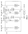
- FIG. 6 is an illustration of a circuit 600 for generating the anti-eclipse threshold voltage AE_Vref in accordance with an exemplary embodiment of the invention.
- the circuit 600 is preferably formed on the same integrated circuit as at least the pixel array 201 and column circuit 220 of an associated imager, but is not otherwise part of the array of pixels generating image signals.
- the circuit 600 generates the anti-eclipse threshold voltage AE_Vref for each of the anti-eclipse circuits 310 ( FIG. 3 ) of an imager 200 .
- portions of the circuit 600 are modifications of pixel circuits (e.g., a non-image pixels whose output would not be further processed).
- the circuit 600 is subject to the same semiconductor fabrication induced variances as the image pixels 100 of the imager 200 , and thus produces an anti-eclipse threshold voltage AE_Vref which can be at a predetermined offset from the reset signal voltage level despite changes to the reset signal voltage level caused by such variances.
- the circuit 600 is organized as three overlapping blocks 601 , 602 , and 603 , an offset voltage generator 630 , and an optional sample-and-hold circuit 650 .
- the circuit 600 includes three power input node A 1 , A 2 , and A 3 , each for accepting pixel power VAAPIX, and three control signal input nodes X 1 , X 2 , and Y, an output signal node Z, and internal nodes C, I+, I ⁇ , IL, and OUT, as further described below.
- Internal node IL is coupled to a load circuit 390 ′.
- Block 601 is preferably a modification of a pixel circuit 100 ( FIG. 1 ) used in the imager associated with circuit 600 .
- Block 601 includes the light sensitive element 101 (which may be a photo-diode shielded from incident light when used in circuit 601 ), N-channel transfer transistor 111 , N-channel reset transistor 112 , N-channel first source follower transistor 113 a , an N-channel first row select transistor 114 a , and the floating diffusion node C.
- the gate of the first source follower transistor 113 a corresponds to internal node I+.
- the gate of the transfer transistor 111 is permanently coupled to a predetermined voltage that causes the transfer transistor 111 to remain off and not conducting, similar to an imaging pixel operation during a reset operation.
- the gate of the transfer transistor 111 is coupled to a ground potential.
- one source/drain of the reset transistor 112 is coupled to pixel power VAAPIX (via node A 1 ) and another source/drain of the reset transistor 112 is coupled to the floating diffusion node C.
- the gate of the reset transistor 112 corresponds to node Y and is coupled to control signal AE_RST, which is a control signal which follows the state of the RST control signal for the selected row in the pixel array 201 ( FIG. 2 ).
- the first source follower transistor 113 a has its gate coupled to the floating diffusion node C, one source/drain coupled to a source/drain of the row select transistor 114 a , and another source/drain coupled to node I 1 , which receives pixel power VAAPIX via transistor 610 and node A 2 of circuit 603 .
- the gate of the first row select transistor 114 a is coupled to node X 1 to receive control signal AE_ROW, which is a control signal that follows the state of the ROW control signal for the selected row in the pixel array 201 .
- Another source/drain of the first row select transistor 114 a is coupled, via node I 2 , to a load circuit 390 ′.
- the function of the portion of block 601 not shared with block 603 is to provide a signal to node I+. That signal is equivalent to a nominal reset signal produced by a pixel 100 ( FIG. 1 ) of the imager 200 ( FIG. 2 ). More specifically, when control signal AE_RST is asserted high to cause transistors 112 to conduct, the signal flowing between to node I+ from node C is equal to the reset signal produced by a pixel 100 under non-eclipse conditions. This signal does not require calibration because the circuit 601 shares a similar design and is fabricated on the same integrated circuit as the pixels 100 of the imager 200 , and thus shares the same semiconductor fabrication inducted variances. Block 601 is not subject to eclipse distortion because its light sensitive element 101 is shielded from incident light.
- Block 602 is also preferably a modification of the pixel circuit 100 ( FIG. 1 ) used in the imager 200 associated with the circuit 600 .
- block 602 includes a second N-channel source follower transistor 113 b and a second N-channel row select transistor 114 b .
- the transistors 113 b and 114 b are coupled in series via their source and drains.
- the gate of the second source follower transistor 113 b corresponds to node I ⁇ , while the source/drain of the second row select transistor 113 b not coupled to the second row select transistor 114 b corresponds to node OUT.
- the gate of the second row select transistor 114 b corresponds to node X 2 .
- the offset voltage generator 630 is coupled between nodes I ⁇ and OUT, and accepts a control signal IN.
- the offset voltage generator 630 is preferably a digital-to-analog converter having a digital input accepting control word IN, a negative output terminal coupled to node OUT, and an analog output coupled to node I ⁇ .
- the offset voltage generator 630 forces a voltage difference, based on the contents of control word IN, between nodes I ⁇ and OUT.
- the digital word may be supplied by a controller, such as controller 260 ( FIG. 2 ) of the imager 200 .
- Block 603 which forms an amplifier in which the positive and negative inputs are respectively applied at terminals I+ and I ⁇ , while the output AE_Vref is supplied at node OUT.
- Node OUT may also be coupled to a sample-and-hold circuit 650 , which could be used to present the AE_Vref voltage at the output of the sample-and-hold circuit.
- Block 603 includes node IL, which is coupled to the source/drains of the first and second row select transistors 114 a , 114 b .
- Node IL is also coupled to load circuit 390 ′, which in one exemplary embodiment comprises a transistor 640 biased to flow twice the current of a standard load circuit 390 .
- FIG. 6B is a simplified diagram useful for explaining the operation of the circuit 600 of FIG. 6A .
- FIG. 6B illustrates an amplifier 6 having positive and negative inputs A+, A ⁇ , and an output O and a battery 7 for creating an offset voltage. If a voltage corresponding to a nominal reset signal level is presented to input A+, the amplifier will output at node O a voltage AE_vref which is lower than the nominal reset signal level by the magnitude of the offset voltage created by the battery.
- the amplifier of block 603 is formed from transistor 610 , 620 , load circuit 390 ′, and certain portions of two modified pixel circuits 601 , 602 .
- the portion of block 601 which does not overlap with block 603 produces the nominal reset signal voltage level.
- the offset voltage is generated by the offset voltage generator 630 .
- Block 603 produces at node OUT the AE_Vref voltage at a voltage level equal to the VAAPIX voltage level minus the offset voltage created by the offset voltage generator 630 .
- FIG. 7 illustrates a processor based system 700 .
- the system 700 is exemplary of a digital system having an imaging device. Without being limited, system 700 could be a part of a computer system, camera, scanner, machine vision system, vehicle or personal navigation system, portable telephone with camera, video phone, surveillance system, auto focus system, optical tracking system, image stabilization system, motion detection system, or other system having an imaging function.
- System 700 for example, a camera, generally comprises a bus 720 .
- Coupled to the bus 720 are a processor, such as CPU 702 , a memory, such as a RAM 704 , a removable memory 714 , an I/O device 706 , and an imager 200 including the circuit 600 of the present invention for generating the reference voltage for its anti-eclipse circuits 310 ( FIG. 3 ).
- a processor such as CPU 702
- a memory such as a RAM 704
- a removable memory 714 such as a removable memory 714
- I/O device 706 an imager 200 including the circuit 600 of the present invention for generating the reference voltage for its anti-eclipse circuits 310 ( FIG. 3 ).
- a method of manufacturing an anti-eclipse circuit includes the steps of providing, over a portion of a substrate corresponding to a single integrated circuit, at least a plurality of imaging pixels 100 , a column circuitry 220 , and circuit 600 .
- the pixels 100 , column circuitry 220 , and circuit 600 can be fabricated on a same integrated circuit using known semiconductor fabrication techniques.
- the present invention therefore takes advantage of the likelihood that modified pixel circuits located on the same integrated circuit as the pixels of the pixel array and the column circuitry of an imager would have identical semiconductor fabrication induced process variances.
- a non-imaging pixel is modified to become part of a reference voltage generator.
- the reference voltage generator is designed to produce a voltage equal to a controllable offset from the ordinary reset signal voltage level of a pixel of the imager, despite differences in such voltage from imager to imager caused by the semiconductor fabrication process.
Abstract
Description
Claims (22)
Priority Applications (16)
| Application Number | Priority Date | Filing Date | Title |
|---|---|---|---|
| US11/100,429 US7916186B2 (en) | 2005-04-07 | 2005-04-07 | Anti-eclipse circuitry with tracking of floating diffusion reset level |
| EP06740489.7A EP1872568B1 (en) | 2005-04-07 | 2006-04-05 | Anti eclipse circuitry with tracking of floating diffusion reset level |
| KR1020077025525A KR100922286B1 (en) | 2005-04-07 | 2006-04-05 | Anti eclipse circuitry with tracking of floating diffusion reset level |
| PCT/US2006/012495 WO2006110396A1 (en) | 2005-04-07 | 2006-04-05 | Anti eclipse circuitry with tracking of floating diffusion reset level |
| JP2008505452A JP4788980B2 (en) | 2005-04-07 | 2006-04-05 | An vignetting prevention circuit having a floating diffusion reset level tracking. |
| CN200680015581XA CN101171829B (en) | 2005-04-07 | 2006-04-05 | Anti-eclipse circuitry with tracking of floating diffusion reset level |
| SG201002097-2A SG161213A1 (en) | 2005-04-07 | 2006-04-05 | Anti-eclipse circuitry with tracking of floating diffusion reset level |
| TW095112569A TWI305356B (en) | 2005-04-07 | 2006-04-07 | Anti-eclipse circuitry with tracking of floating diffusion reset level and method thereof |
| US13/029,613 US8547462B2 (en) | 2005-04-07 | 2011-02-17 | Anti-eclipse circuitry with tracking of floating diffusion reset level |
| US14/038,277 US9185315B2 (en) | 2005-04-07 | 2013-09-26 | Anti-eclipse circuitry with tracking of floating diffusion reset level |
| US14/936,449 US9838624B2 (en) | 2005-04-07 | 2015-11-09 | Anti-eclipse circuitry with tracking of floating diffusion reset level |
| US15/803,690 US10122952B2 (en) | 2005-04-07 | 2017-11-03 | Anti-eclipse circuitry with tracking of floating diffusion reset level |
| US16/147,990 US10462399B2 (en) | 2005-04-07 | 2018-10-01 | Anti-eclipse circuitry with tracking of floating diffusion reset level |
| US16/653,605 US11245862B2 (en) | 2005-04-07 | 2019-10-15 | Anti-eclipse circuitry with tracking of floating diffusion reset level |
| US17/579,446 US11647303B2 (en) | 2005-04-07 | 2022-01-19 | Anti-eclipse circuitry with tracking of floating diffusion reset level |
| US18/189,464 US20230300480A1 (en) | 2005-04-07 | 2023-03-24 | Anti-eclipse circuitry with tracking of floating diffusion reset level |
Applications Claiming Priority (1)
| Application Number | Priority Date | Filing Date | Title |
|---|---|---|---|
| US11/100,429 US7916186B2 (en) | 2005-04-07 | 2005-04-07 | Anti-eclipse circuitry with tracking of floating diffusion reset level |
Related Child Applications (1)
| Application Number | Title | Priority Date | Filing Date |
|---|---|---|---|
| US13/029,613 Division US8547462B2 (en) | 2005-04-07 | 2011-02-17 | Anti-eclipse circuitry with tracking of floating diffusion reset level |
Publications (2)
| Publication Number | Publication Date |
|---|---|
| US20060227226A1 US20060227226A1 (en) | 2006-10-12 |
| US7916186B2 true US7916186B2 (en) | 2011-03-29 |
Family
ID=36609050
Family Applications (9)
| Application Number | Title | Priority Date | Filing Date |
|---|---|---|---|
| US11/100,429 Active 2028-02-06 US7916186B2 (en) | 2005-04-07 | 2005-04-07 | Anti-eclipse circuitry with tracking of floating diffusion reset level |
| US13/029,613 Active 2025-08-11 US8547462B2 (en) | 2005-04-07 | 2011-02-17 | Anti-eclipse circuitry with tracking of floating diffusion reset level |
| US14/038,277 Active 2025-11-17 US9185315B2 (en) | 2005-04-07 | 2013-09-26 | Anti-eclipse circuitry with tracking of floating diffusion reset level |
| US14/936,449 Active 2025-05-22 US9838624B2 (en) | 2005-04-07 | 2015-11-09 | Anti-eclipse circuitry with tracking of floating diffusion reset level |
| US15/803,690 Active US10122952B2 (en) | 2005-04-07 | 2017-11-03 | Anti-eclipse circuitry with tracking of floating diffusion reset level |
| US16/147,990 Active US10462399B2 (en) | 2005-04-07 | 2018-10-01 | Anti-eclipse circuitry with tracking of floating diffusion reset level |
| US16/653,605 Active 2025-07-27 US11245862B2 (en) | 2005-04-07 | 2019-10-15 | Anti-eclipse circuitry with tracking of floating diffusion reset level |
| US17/579,446 Active US11647303B2 (en) | 2005-04-07 | 2022-01-19 | Anti-eclipse circuitry with tracking of floating diffusion reset level |
| US18/189,464 Pending US20230300480A1 (en) | 2005-04-07 | 2023-03-24 | Anti-eclipse circuitry with tracking of floating diffusion reset level |
Family Applications After (8)
| Application Number | Title | Priority Date | Filing Date |
|---|---|---|---|
| US13/029,613 Active 2025-08-11 US8547462B2 (en) | 2005-04-07 | 2011-02-17 | Anti-eclipse circuitry with tracking of floating diffusion reset level |
| US14/038,277 Active 2025-11-17 US9185315B2 (en) | 2005-04-07 | 2013-09-26 | Anti-eclipse circuitry with tracking of floating diffusion reset level |
| US14/936,449 Active 2025-05-22 US9838624B2 (en) | 2005-04-07 | 2015-11-09 | Anti-eclipse circuitry with tracking of floating diffusion reset level |
| US15/803,690 Active US10122952B2 (en) | 2005-04-07 | 2017-11-03 | Anti-eclipse circuitry with tracking of floating diffusion reset level |
| US16/147,990 Active US10462399B2 (en) | 2005-04-07 | 2018-10-01 | Anti-eclipse circuitry with tracking of floating diffusion reset level |
| US16/653,605 Active 2025-07-27 US11245862B2 (en) | 2005-04-07 | 2019-10-15 | Anti-eclipse circuitry with tracking of floating diffusion reset level |
| US17/579,446 Active US11647303B2 (en) | 2005-04-07 | 2022-01-19 | Anti-eclipse circuitry with tracking of floating diffusion reset level |
| US18/189,464 Pending US20230300480A1 (en) | 2005-04-07 | 2023-03-24 | Anti-eclipse circuitry with tracking of floating diffusion reset level |
Country Status (8)
| Country | Link |
|---|---|
| US (9) | US7916186B2 (en) |
| EP (1) | EP1872568B1 (en) |
| JP (1) | JP4788980B2 (en) |
| KR (1) | KR100922286B1 (en) |
| CN (1) | CN101171829B (en) |
| SG (1) | SG161213A1 (en) |
| TW (1) | TWI305356B (en) |
| WO (1) | WO2006110396A1 (en) |
Cited By (2)
| Publication number | Priority date | Publication date | Assignee | Title |
|---|---|---|---|---|
| US10462399B2 (en) * | 2005-04-07 | 2019-10-29 | Micron Technology, Inc. | Anti-eclipse circuitry with tracking of floating diffusion reset level |
| US11361469B2 (en) * | 2016-09-07 | 2022-06-14 | Starship Technologies Oü | Method and system for calibrating multiple cameras |
Families Citing this family (19)
| Publication number | Priority date | Publication date | Assignee | Title |
|---|---|---|---|---|
| JP4534804B2 (en) * | 2005-03-09 | 2010-09-01 | ソニー株式会社 | Imaging device |
| FR2914499B1 (en) * | 2007-04-02 | 2009-05-29 | St Microelectronics Sa | METHOD AND CIRCUIT FOR OBTAINING A SAMPLE IN AN IMAGE SENSOR |
| US7872676B2 (en) * | 2007-07-13 | 2011-01-18 | Micron Technology, Inc. | Methods, systems, and devices for offset compensation in CMOC imagers |
| JP5203913B2 (en) * | 2008-12-15 | 2013-06-05 | キヤノン株式会社 | Photoelectric conversion device, imaging system, and driving method of photoelectric conversion device |
| JP5531417B2 (en) | 2009-02-12 | 2014-06-25 | 株式会社ニコン | Solid-state imaging device |
| JP2010220111A (en) * | 2009-03-18 | 2010-09-30 | Toshiba Corp | Clamp circuit and solid-state imaging apparatus with same |
| GB2496135B (en) | 2011-11-01 | 2015-03-18 | Valirx Plc | Inhibitors of the interaction between a Src family kinase and an androgen receptor or estradiol receptor for treatment of endometriosis |
| CN102508432B (en) * | 2011-11-04 | 2014-04-02 | 国电南京自动化股份有限公司 | Automatic control steady-state undisturbed switching method for desulphurization booster fan |
| US9380232B2 (en) | 2014-02-20 | 2016-06-28 | Semiconductor Components Industries, Llc | Image sensors with anti-eclipse circuitry |
| JP6418775B2 (en) * | 2014-04-18 | 2018-11-07 | キヤノン株式会社 | Photoelectric conversion device, imaging system, and driving method of photoelectric conversion device |
| KR101685077B1 (en) * | 2015-08-18 | 2016-12-09 | 연세대학교 산학협력단 | gain-linearized pixel merged open loop pre-amplifier for small pixel |
| US9973717B1 (en) | 2016-12-28 | 2018-05-15 | Semiconductor Components Industries, Llc | Image sensors with anti-eclipse circuitry |
| US10630926B2 (en) * | 2017-06-03 | 2020-04-21 | Himax Imaging Limited | Anti-eclipse circuit and related imager |
| US10582138B2 (en) | 2017-09-22 | 2020-03-03 | Semiconductor Components Industries, Llc | Image sensors with dual conversion gain pixels and anti-eclipse circuitry |
| US10477126B1 (en) | 2018-09-05 | 2019-11-12 | Smartsens Technology (Cayman) Co., Limited | Dual eclipse circuit for reduced image sensor shading |
| US10873716B2 (en) | 2018-11-05 | 2020-12-22 | SmartSens Technology (HK) Co., Ltd. | Dual row control signal circuit for reduced image sensor shading |
| US10727268B1 (en) | 2019-01-25 | 2020-07-28 | Smartsens Technology (Cayman) Co., Ltd | CMOS image sensor with compact pixel layout |
| US10652492B1 (en) | 2019-02-12 | 2020-05-12 | Smartsens Technology (Cayman) Co., Ltd. | CMOS image sensor with improved column data shift readout |
| CN110896082A (en) | 2019-05-28 | 2020-03-20 | 思特威(上海)电子科技有限公司 | Image sensor with novel layout |
Citations (19)
| Publication number | Priority date | Publication date | Assignee | Title |
|---|---|---|---|---|
| US5523570A (en) * | 1994-07-15 | 1996-06-04 | Loral Infrared & Imaging Systems, Inc. | Double direct injection dual band sensor readout input circuit |
| JPH10164442A (en) | 1996-12-02 | 1998-06-19 | Texas Instr Japan Ltd | Correlated double sampling circuit |
| JP2000287131A (en) | 1998-12-25 | 2000-10-13 | Toshiba Corp | Solid-state image pickup device |
| JP2001024947A (en) | 1999-07-07 | 2001-01-26 | Canon Inc | Photoelectric conversion chip, image sensor and image sensor unit |
| US6452152B1 (en) | 2000-02-22 | 2002-09-17 | Pixim, Inc. | Sense amplifier having a precision analog reference level for use with image sensors |
| US20030080279A1 (en) * | 1999-08-16 | 2003-05-01 | Morteza Afghahi | Offset reduction in image sensors |
| US20030179159A1 (en) * | 2002-03-01 | 2003-09-25 | Shinji Ohsawa | Solid state image sensor with signal line potential adjustment circuit and method of driving the same |
| JP2004007394A (en) | 2002-01-17 | 2004-01-08 | Zoran Corp | Complementary metal oxided semiconductor sensor equipped with supersaturation reducing function |
| US20040036783A1 (en) | 2002-08-22 | 2004-02-26 | Barna Sandor L. | Asymmetric comparator for use in pixel oversaturation detection |
| JP2004222273A (en) | 2003-01-13 | 2004-08-05 | Hynix Semiconductor Inc | Image sensor with clamp circuit |
| CN1534793A (en) | 2003-03-31 | 2004-10-06 | 松下电器产业株式会社 | Solid imaging apparatus and mfg. method thereof |
| JP2004320346A (en) | 2003-04-15 | 2004-11-11 | Olympus Corp | Solid state imaging apparatus |
| US20050168607A1 (en) * | 2004-02-04 | 2005-08-04 | June-Soo Han | Apparatus and method for clamping reset voltage in image sensor |
| US20050237400A1 (en) * | 2004-04-23 | 2005-10-27 | Daniel Van Blerkom | Image sensor and offset-able reference voltage generator thereof |
| US7075474B2 (en) * | 2004-07-02 | 2006-07-11 | Fujitsu Limited | Ramp waveform generation circuit, analog/digital conversion circuit, imaging device and control method of imaging device |
| US7170556B2 (en) * | 2002-07-25 | 2007-01-30 | Fujitsu Limited | Image sensor providing improved image quality |
| US7280140B2 (en) * | 2002-04-02 | 2007-10-09 | Stmicroelectronics Ltd. | Image sensor reading during reset and reading on release from reset |
| US7304674B2 (en) * | 2002-11-15 | 2007-12-04 | Avago Technologies General Ip Pte Ltd | Sampling image signals generated by pixel circuits of an active pixel sensor (APS) image sensor in a sub-sampling mode |
| US7385636B2 (en) * | 2004-04-30 | 2008-06-10 | Eastman Kodak Company | Low noise sample and hold circuit for image sensors |
Family Cites Families (23)
| Publication number | Priority date | Publication date | Assignee | Title |
|---|---|---|---|---|
| US6542183B1 (en) * | 1995-06-28 | 2003-04-01 | Lynx Systems Developers, Inc. | Event recording apparatus |
| JP3014281B2 (en) * | 1994-09-22 | 2000-02-28 | インターナショナル・ビジネス・マシーンズ・コーポレイション | Synchronous signal separation circuit, synchronous signal separation method |
| US6175383B1 (en) * | 1996-11-07 | 2001-01-16 | California Institute Of Technology | Method and apparatus of high dynamic range image sensor with individual pixel reset |
| JP3177187B2 (en) * | 1997-05-14 | 2001-06-18 | 株式会社東芝 | Correction device, correction method, image reading device, and image forming device |
| US6335088B1 (en) | 1998-07-06 | 2002-01-01 | Daiya Pharmaceutical Co., Ltd. | Moisture-retentive cooling gel, moisture-retentive cooling gel laminate, and moisture-retentive cooling plaster |
| US6774941B1 (en) * | 1999-10-26 | 2004-08-10 | National Semiconductor Corporation | CCD output processing stage that amplifies signals from colored pixels based on the conversion efficiency of the colored pixels |
| US6486504B1 (en) * | 1999-10-26 | 2002-11-26 | Eastman Kodak Company | CMOS image sensor with extended dynamic range |
| EP1143706A3 (en) * | 2000-03-28 | 2007-08-01 | Fujitsu Limited | Image sensor with black level control and low power consumption |
| US6806901B1 (en) * | 2000-10-31 | 2004-10-19 | Texas Instruments Incorporated | Controlling the range and resolution of offset correction applied to the output of a charge coupled device |
| US6816196B1 (en) * | 2001-06-18 | 2004-11-09 | Ess Technology, Inc. | CMOS imager with quantized correlated double sampling |
| US6927433B2 (en) * | 2001-06-28 | 2005-08-09 | Isetec, Inc | Active pixel image sensor with two transistor pixel, in-pixel non-uniformity correction, and bootstrapped reset lines |
| US6861634B2 (en) * | 2002-08-13 | 2005-03-01 | Micron Technology, Inc. | CMOS active pixel sensor with a sample and hold circuit having multiple injection capacitors and a fully differential charge mode linear synthesizer with skew control |
| US7129883B2 (en) * | 2004-02-23 | 2006-10-31 | Sony Corporation | Method and apparatus for AD conversion, semiconductor device for detecting distribution of physical quantity, and electronic apparatus |
| US7477298B2 (en) * | 2004-08-30 | 2009-01-13 | Micron Technology, Inc. | Anti-eclipsing circuit for image sensors |
| JP4914019B2 (en) * | 2005-04-06 | 2012-04-11 | キヤノン株式会社 | Position and orientation measurement method and apparatus |
| US7916186B2 (en) | 2005-04-07 | 2011-03-29 | Micron Technology, Inc. | Anti-eclipse circuitry with tracking of floating diffusion reset level |
| US7872682B2 (en) * | 2005-05-10 | 2011-01-18 | Micron Technology, Inc. | Eclipse elimination by monitoring the pixel signal level |
| US7573519B2 (en) * | 2005-10-26 | 2009-08-11 | Eastman Kodak Company | Method for correcting eclipse or darkle |
| US8081837B2 (en) * | 2006-02-07 | 2011-12-20 | Intel Corporation | Image sensor array leakage and dark current compensation |
| KR100790982B1 (en) * | 2006-02-14 | 2008-01-03 | 삼성전자주식회사 | Image sensor compensating the reset signal level of active pixel using the average value of the reset signal level of optical black pixel and the method of compensating the reset signal level of active pixel of the image sensor |
| US7777783B1 (en) * | 2007-03-23 | 2010-08-17 | Proximex Corporation | Multi-video navigation |
| US8077240B2 (en) * | 2008-04-23 | 2011-12-13 | Inernational Business Machines Corporation | Methods for enhancing quality of pixel sensor image frames for global shutter imaging |
| TW201517625A (en) * | 2013-10-30 | 2015-05-01 | Novatek Microelectronics Corp | Image sensing apparatus and black level controlling method thereof |
-
2005
- 2005-04-07 US US11/100,429 patent/US7916186B2/en active Active
-
2006
- 2006-04-05 WO PCT/US2006/012495 patent/WO2006110396A1/en active Application Filing
- 2006-04-05 CN CN200680015581XA patent/CN101171829B/en active Active
- 2006-04-05 SG SG201002097-2A patent/SG161213A1/en unknown
- 2006-04-05 EP EP06740489.7A patent/EP1872568B1/en active Active
- 2006-04-05 JP JP2008505452A patent/JP4788980B2/en active Active
- 2006-04-05 KR KR1020077025525A patent/KR100922286B1/en active IP Right Grant
- 2006-04-07 TW TW095112569A patent/TWI305356B/en active
-
2011
- 2011-02-17 US US13/029,613 patent/US8547462B2/en active Active
-
2013
- 2013-09-26 US US14/038,277 patent/US9185315B2/en active Active
-
2015
- 2015-11-09 US US14/936,449 patent/US9838624B2/en active Active
-
2017
- 2017-11-03 US US15/803,690 patent/US10122952B2/en active Active
-
2018
- 2018-10-01 US US16/147,990 patent/US10462399B2/en active Active
-
2019
- 2019-10-15 US US16/653,605 patent/US11245862B2/en active Active
-
2022
- 2022-01-19 US US17/579,446 patent/US11647303B2/en active Active
-
2023
- 2023-03-24 US US18/189,464 patent/US20230300480A1/en active Pending
Patent Citations (21)
| Publication number | Priority date | Publication date | Assignee | Title |
|---|---|---|---|---|
| US5523570A (en) * | 1994-07-15 | 1996-06-04 | Loral Infrared & Imaging Systems, Inc. | Double direct injection dual band sensor readout input circuit |
| JPH10164442A (en) | 1996-12-02 | 1998-06-19 | Texas Instr Japan Ltd | Correlated double sampling circuit |
| JP2000287131A (en) | 1998-12-25 | 2000-10-13 | Toshiba Corp | Solid-state image pickup device |
| JP2001024947A (en) | 1999-07-07 | 2001-01-26 | Canon Inc | Photoelectric conversion chip, image sensor and image sensor unit |
| US20030080279A1 (en) * | 1999-08-16 | 2003-05-01 | Morteza Afghahi | Offset reduction in image sensors |
| US6452152B1 (en) | 2000-02-22 | 2002-09-17 | Pixim, Inc. | Sense amplifier having a precision analog reference level for use with image sensors |
| JP2004007394A (en) | 2002-01-17 | 2004-01-08 | Zoran Corp | Complementary metal oxided semiconductor sensor equipped with supersaturation reducing function |
| US20030179159A1 (en) * | 2002-03-01 | 2003-09-25 | Shinji Ohsawa | Solid state image sensor with signal line potential adjustment circuit and method of driving the same |
| US7280140B2 (en) * | 2002-04-02 | 2007-10-09 | Stmicroelectronics Ltd. | Image sensor reading during reset and reading on release from reset |
| US7170556B2 (en) * | 2002-07-25 | 2007-01-30 | Fujitsu Limited | Image sensor providing improved image quality |
| US20040036783A1 (en) | 2002-08-22 | 2004-02-26 | Barna Sandor L. | Asymmetric comparator for use in pixel oversaturation detection |
| US7304674B2 (en) * | 2002-11-15 | 2007-12-04 | Avago Technologies General Ip Pte Ltd | Sampling image signals generated by pixel circuits of an active pixel sensor (APS) image sensor in a sub-sampling mode |
| JP2004222273A (en) | 2003-01-13 | 2004-08-05 | Hynix Semiconductor Inc | Image sensor with clamp circuit |
| CN1534793A (en) | 2003-03-31 | 2004-10-06 | 松下电器产业株式会社 | Solid imaging apparatus and mfg. method thereof |
| EP1840969A1 (en) | 2003-03-31 | 2007-10-03 | Matsushita Electric Industrial Co., Ltd. | Solid-state imaging apparatus and method for producing the same |
| JP2004320346A (en) | 2003-04-15 | 2004-11-11 | Olympus Corp | Solid state imaging apparatus |
| JP2005223908A (en) | 2004-02-04 | 2005-08-18 | Samsung Electronics Co Ltd | Clamp circuit for cmos image sensor |
| US20050168607A1 (en) * | 2004-02-04 | 2005-08-04 | June-Soo Han | Apparatus and method for clamping reset voltage in image sensor |
| US20050237400A1 (en) * | 2004-04-23 | 2005-10-27 | Daniel Van Blerkom | Image sensor and offset-able reference voltage generator thereof |
| US7385636B2 (en) * | 2004-04-30 | 2008-06-10 | Eastman Kodak Company | Low noise sample and hold circuit for image sensors |
| US7075474B2 (en) * | 2004-07-02 | 2006-07-11 | Fujitsu Limited | Ramp waveform generation circuit, analog/digital conversion circuit, imaging device and control method of imaging device |
Non-Patent Citations (2)
| Title |
|---|
| Chinese Office Action for CN 200680015581.X, Aug. 28, 2009. |
| Office Action with Translation for Korean Patent Application 10-2007-7025525 dated May 4, 2009. |
Cited By (7)
| Publication number | Priority date | Publication date | Assignee | Title |
|---|---|---|---|---|
| US10462399B2 (en) * | 2005-04-07 | 2019-10-29 | Micron Technology, Inc. | Anti-eclipse circuitry with tracking of floating diffusion reset level |
| US11245862B2 (en) * | 2005-04-07 | 2022-02-08 | Micron Technology, Inc. | Anti-eclipse circuitry with tracking of floating diffusion reset level |
| US20220150426A1 (en) * | 2005-04-07 | 2022-05-12 | Micron Technology, Inc. | Anti-eclipse circuitry with tracking of floating diffusion reset level |
| US11647303B2 (en) * | 2005-04-07 | 2023-05-09 | Micron Technology, Inc. | Anti-eclipse circuitry with tracking of floating diffusion reset level |
| US20230300480A1 (en) * | 2005-04-07 | 2023-09-21 | Micron Technology, Inc. | Anti-eclipse circuitry with tracking of floating diffusion reset level |
| US11361469B2 (en) * | 2016-09-07 | 2022-06-14 | Starship Technologies Oü | Method and system for calibrating multiple cameras |
| US20220292720A1 (en) * | 2016-09-07 | 2022-09-15 | Starship Technologies Oü | Method and system for calibrating multiple cameras |
Also Published As
| Publication number | Publication date |
|---|---|
| EP1872568B1 (en) | 2018-08-08 |
| US10122952B2 (en) | 2018-11-06 |
| CN101171829A (en) | 2008-04-30 |
| US20200045254A1 (en) | 2020-02-06 |
| US20160065868A1 (en) | 2016-03-03 |
| WO2006110396A1 (en) | 2006-10-19 |
| US8547462B2 (en) | 2013-10-01 |
| TW200643957A (en) | 2006-12-16 |
| US20140022429A1 (en) | 2014-01-23 |
| US9185315B2 (en) | 2015-11-10 |
| US20180063452A1 (en) | 2018-03-01 |
| EP1872568A1 (en) | 2008-01-02 |
| US20220150426A1 (en) | 2022-05-12 |
| US10462399B2 (en) | 2019-10-29 |
| US20230300480A1 (en) | 2023-09-21 |
| US20190045148A1 (en) | 2019-02-07 |
| KR100922286B1 (en) | 2009-10-15 |
| JP4788980B2 (en) | 2011-10-05 |
| US20110133057A1 (en) | 2011-06-09 |
| CN101171829B (en) | 2012-11-28 |
| US11647303B2 (en) | 2023-05-09 |
| KR20070118179A (en) | 2007-12-13 |
| TWI305356B (en) | 2009-01-11 |
| JP2008536396A (en) | 2008-09-04 |
| US9838624B2 (en) | 2017-12-05 |
| US11245862B2 (en) | 2022-02-08 |
| US20060227226A1 (en) | 2006-10-12 |
| SG161213A1 (en) | 2010-05-27 |
Similar Documents
| Publication | Publication Date | Title |
|---|---|---|
| US11647303B2 (en) | Anti-eclipse circuitry with tracking of floating diffusion reset level | |
| US8013915B2 (en) | Anti-eclipsing circuit for image sensors | |
| US7872682B2 (en) | Eclipse elimination by monitoring the pixel signal level | |
| US7710471B2 (en) | Pixel individual anti-eclipse circuit and its operation manner | |
| US20120044396A1 (en) | Dual pinned diode pixel with shutter | |
| US7659928B2 (en) | Apparatus and method for providing anti-eclipse operation for imaging sensors | |
| US6999122B1 (en) | Solid-state logarithmic image sensing device | |
| CN111147774B (en) | System and method for voltage stabilization |
Legal Events
| Date | Code | Title | Description |
|---|---|---|---|
| AS | Assignment |
Owner name: MICRON TECHNOLOGY, INC., IDAHO Free format text: ASSIGNMENT OF ASSIGNORS INTEREST;ASSIGNOR:OLSEN, ESPEN A.;REEL/FRAME:016457/0224 Effective date: 20050331 |
|
| FEPP | Fee payment procedure |
Free format text: PAYOR NUMBER ASSIGNED (ORIGINAL EVENT CODE: ASPN); ENTITY STATUS OF PATENT OWNER: LARGE ENTITY |
|
| STCF | Information on status: patent grant |
Free format text: PATENTED CASE |
|
| FPAY | Fee payment |
Year of fee payment: 4 |
|
| AS | Assignment |
Owner name: U.S. BANK NATIONAL ASSOCIATION, AS COLLATERAL AGENT, CALIFORNIA Free format text: SECURITY INTEREST;ASSIGNOR:MICRON TECHNOLOGY, INC.;REEL/FRAME:038669/0001 Effective date: 20160426 Owner name: U.S. BANK NATIONAL ASSOCIATION, AS COLLATERAL AGEN Free format text: SECURITY INTEREST;ASSIGNOR:MICRON TECHNOLOGY, INC.;REEL/FRAME:038669/0001 Effective date: 20160426 |
|
| AS | Assignment |
Owner name: MORGAN STANLEY SENIOR FUNDING, INC., AS COLLATERAL AGENT, MARYLAND Free format text: PATENT SECURITY AGREEMENT;ASSIGNOR:MICRON TECHNOLOGY, INC.;REEL/FRAME:038954/0001 Effective date: 20160426 Owner name: MORGAN STANLEY SENIOR FUNDING, INC., AS COLLATERAL Free format text: PATENT SECURITY AGREEMENT;ASSIGNOR:MICRON TECHNOLOGY, INC.;REEL/FRAME:038954/0001 Effective date: 20160426 |
|
| AS | Assignment |
Owner name: U.S. BANK NATIONAL ASSOCIATION, AS COLLATERAL AGENT, CALIFORNIA Free format text: CORRECTIVE ASSIGNMENT TO CORRECT THE REPLACE ERRONEOUSLY FILED PATENT #7358718 WITH THE CORRECT PATENT #7358178 PREVIOUSLY RECORDED ON REEL 038669 FRAME 0001. ASSIGNOR(S) HEREBY CONFIRMS THE SECURITY INTEREST;ASSIGNOR:MICRON TECHNOLOGY, INC.;REEL/FRAME:043079/0001 Effective date: 20160426 Owner name: U.S. BANK NATIONAL ASSOCIATION, AS COLLATERAL AGEN Free format text: CORRECTIVE ASSIGNMENT TO CORRECT THE REPLACE ERRONEOUSLY FILED PATENT #7358718 WITH THE CORRECT PATENT #7358178 PREVIOUSLY RECORDED ON REEL 038669 FRAME 0001. ASSIGNOR(S) HEREBY CONFIRMS THE SECURITY INTEREST;ASSIGNOR:MICRON TECHNOLOGY, INC.;REEL/FRAME:043079/0001 Effective date: 20160426 |
|
| AS | Assignment |
Owner name: JPMORGAN CHASE BANK, N.A., AS COLLATERAL AGENT, ILLINOIS Free format text: SECURITY INTEREST;ASSIGNORS:MICRON TECHNOLOGY, INC.;MICRON SEMICONDUCTOR PRODUCTS, INC.;REEL/FRAME:047540/0001 Effective date: 20180703 Owner name: JPMORGAN CHASE BANK, N.A., AS COLLATERAL AGENT, IL Free format text: SECURITY INTEREST;ASSIGNORS:MICRON TECHNOLOGY, INC.;MICRON SEMICONDUCTOR PRODUCTS, INC.;REEL/FRAME:047540/0001 Effective date: 20180703 |
|
| AS | Assignment |
Owner name: MICRON TECHNOLOGY, INC., IDAHO Free format text: RELEASE BY SECURED PARTY;ASSIGNOR:U.S. BANK NATIONAL ASSOCIATION, AS COLLATERAL AGENT;REEL/FRAME:047243/0001 Effective date: 20180629 |
|
| MAFP | Maintenance fee payment |
Free format text: PAYMENT OF MAINTENANCE FEE, 8TH YEAR, LARGE ENTITY (ORIGINAL EVENT CODE: M1552); ENTITY STATUS OF PATENT OWNER: LARGE ENTITY Year of fee payment: 8 |
|
| AS | Assignment |
Owner name: MICRON TECHNOLOGY, INC., IDAHO Free format text: RELEASE BY SECURED PARTY;ASSIGNOR:MORGAN STANLEY SENIOR FUNDING, INC., AS COLLATERAL AGENT;REEL/FRAME:050937/0001 Effective date: 20190731 |
|
| AS | Assignment |
Owner name: MICRON SEMICONDUCTOR PRODUCTS, INC., IDAHO Free format text: RELEASE BY SECURED PARTY;ASSIGNOR:JPMORGAN CHASE BANK, N.A., AS COLLATERAL AGENT;REEL/FRAME:051028/0001 Effective date: 20190731 Owner name: MICRON TECHNOLOGY, INC., IDAHO Free format text: RELEASE BY SECURED PARTY;ASSIGNOR:JPMORGAN CHASE BANK, N.A., AS COLLATERAL AGENT;REEL/FRAME:051028/0001 Effective date: 20190731 |
|
| MAFP | Maintenance fee payment |
Free format text: PAYMENT OF MAINTENANCE FEE, 12TH YEAR, LARGE ENTITY (ORIGINAL EVENT CODE: M1553); ENTITY STATUS OF PATENT OWNER: LARGE ENTITY Year of fee payment: 12 |