US7816788B2 - Structure, method and system for assessing bonding of electrodes in FCB packaging - Google Patents
Structure, method and system for assessing bonding of electrodes in FCB packaging Download PDFInfo
- Publication number
- US7816788B2 US7816788B2 US12/122,556 US12255608A US7816788B2 US 7816788 B2 US7816788 B2 US 7816788B2 US 12255608 A US12255608 A US 12255608A US 7816788 B2 US7816788 B2 US 7816788B2
- Authority
- US
- United States
- Prior art keywords
- shape
- electrode
- semiconductor device
- solder bump
- bonding
- Prior art date
- Legal status (The legal status is an assumption and is not a legal conclusion. Google has not performed a legal analysis and makes no representation as to the accuracy of the status listed.)
- Expired - Fee Related, expires
Links
Images


Classifications
-
- H—ELECTRICITY
- H01—ELECTRIC ELEMENTS
- H01L—SEMICONDUCTOR DEVICES NOT COVERED BY CLASS H10
- H01L24/00—Arrangements for connecting or disconnecting semiconductor or solid-state bodies; Methods or apparatus related thereto
- H01L24/01—Means for bonding being attached to, or being formed on, the surface to be connected, e.g. chip-to-package, die-attach, "first-level" interconnects; Manufacturing methods related thereto
- H01L24/02—Bonding areas ; Manufacturing methods related thereto
- H01L24/04—Structure, shape, material or disposition of the bonding areas prior to the connecting process
- H01L24/05—Structure, shape, material or disposition of the bonding areas prior to the connecting process of an individual bonding area
-
- H—ELECTRICITY
- H01—ELECTRIC ELEMENTS
- H01L—SEMICONDUCTOR DEVICES NOT COVERED BY CLASS H10
- H01L22/00—Testing or measuring during manufacture or treatment; Reliability measurements, i.e. testing of parts without further processing to modify the parts as such; Structural arrangements therefor
- H01L22/20—Sequence of activities consisting of a plurality of measurements, corrections, marking or sorting steps
- H01L22/24—Optical enhancement of defects or not directly visible states, e.g. selective electrolytic deposition, bubbles in liquids, light emission, colour change
-
- H—ELECTRICITY
- H01—ELECTRIC ELEMENTS
- H01L—SEMICONDUCTOR DEVICES NOT COVERED BY CLASS H10
- H01L23/00—Details of semiconductor or other solid state devices
- H01L23/544—Marks applied to semiconductor devices or parts, e.g. registration marks, alignment structures, wafer maps
-
- H—ELECTRICITY
- H01—ELECTRIC ELEMENTS
- H01L—SEMICONDUCTOR DEVICES NOT COVERED BY CLASS H10
- H01L24/00—Arrangements for connecting or disconnecting semiconductor or solid-state bodies; Methods or apparatus related thereto
- H01L24/01—Means for bonding being attached to, or being formed on, the surface to be connected, e.g. chip-to-package, die-attach, "first-level" interconnects; Manufacturing methods related thereto
- H01L24/02—Bonding areas ; Manufacturing methods related thereto
- H01L24/04—Structure, shape, material or disposition of the bonding areas prior to the connecting process
- H01L24/06—Structure, shape, material or disposition of the bonding areas prior to the connecting process of a plurality of bonding areas
-
- H—ELECTRICITY
- H01—ELECTRIC ELEMENTS
- H01L—SEMICONDUCTOR DEVICES NOT COVERED BY CLASS H10
- H01L24/00—Arrangements for connecting or disconnecting semiconductor or solid-state bodies; Methods or apparatus related thereto
- H01L24/01—Means for bonding being attached to, or being formed on, the surface to be connected, e.g. chip-to-package, die-attach, "first-level" interconnects; Manufacturing methods related thereto
- H01L24/10—Bump connectors ; Manufacturing methods related thereto
- H01L24/15—Structure, shape, material or disposition of the bump connectors after the connecting process
- H01L24/17—Structure, shape, material or disposition of the bump connectors after the connecting process of a plurality of bump connectors
-
- H—ELECTRICITY
- H01—ELECTRIC ELEMENTS
- H01L—SEMICONDUCTOR DEVICES NOT COVERED BY CLASS H10
- H01L24/00—Arrangements for connecting or disconnecting semiconductor or solid-state bodies; Methods or apparatus related thereto
- H01L24/80—Methods for connecting semiconductor or other solid state bodies using means for bonding being attached to, or being formed on, the surface to be connected
- H01L24/81—Methods for connecting semiconductor or other solid state bodies using means for bonding being attached to, or being formed on, the surface to be connected using a bump connector
-
- H—ELECTRICITY
- H05—ELECTRIC TECHNIQUES NOT OTHERWISE PROVIDED FOR
- H05K—PRINTED CIRCUITS; CASINGS OR CONSTRUCTIONAL DETAILS OF ELECTRIC APPARATUS; MANUFACTURE OF ASSEMBLAGES OF ELECTRICAL COMPONENTS
- H05K3/00—Apparatus or processes for manufacturing printed circuits
- H05K3/30—Assembling printed circuits with electric components, e.g. with resistor
- H05K3/32—Assembling printed circuits with electric components, e.g. with resistor electrically connecting electric components or wires to printed circuits
- H05K3/34—Assembling printed circuits with electric components, e.g. with resistor electrically connecting electric components or wires to printed circuits by soldering
- H05K3/341—Surface mounted components
- H05K3/3431—Leadless components
- H05K3/3436—Leadless components having an array of bottom contacts, e.g. pad grid array or ball grid array components
-
- H—ELECTRICITY
- H01—ELECTRIC ELEMENTS
- H01L—SEMICONDUCTOR DEVICES NOT COVERED BY CLASS H10
- H01L2223/00—Details relating to semiconductor or other solid state devices covered by the group H01L23/00
- H01L2223/544—Marks applied to semiconductor devices or parts
- H01L2223/5442—Marks applied to semiconductor devices or parts comprising non digital, non alphanumeric information, e.g. symbols
-
- H—ELECTRICITY
- H01—ELECTRIC ELEMENTS
- H01L—SEMICONDUCTOR DEVICES NOT COVERED BY CLASS H10
- H01L2223/00—Details relating to semiconductor or other solid state devices covered by the group H01L23/00
- H01L2223/544—Marks applied to semiconductor devices or parts
- H01L2223/54473—Marks applied to semiconductor devices or parts for use after dicing
- H01L2223/5448—Located on chip prior to dicing and remaining on chip after dicing
-
- H—ELECTRICITY
- H01—ELECTRIC ELEMENTS
- H01L—SEMICONDUCTOR DEVICES NOT COVERED BY CLASS H10
- H01L2224/00—Indexing scheme for arrangements for connecting or disconnecting semiconductor or solid-state bodies and methods related thereto as covered by H01L24/00
- H01L2224/01—Means for bonding being attached to, or being formed on, the surface to be connected, e.g. chip-to-package, die-attach, "first-level" interconnects; Manufacturing methods related thereto
- H01L2224/02—Bonding areas; Manufacturing methods related thereto
- H01L2224/04—Structure, shape, material or disposition of the bonding areas prior to the connecting process
- H01L2224/0401—Bonding areas specifically adapted for bump connectors, e.g. under bump metallisation [UBM]
-
- H—ELECTRICITY
- H01—ELECTRIC ELEMENTS
- H01L—SEMICONDUCTOR DEVICES NOT COVERED BY CLASS H10
- H01L2224/00—Indexing scheme for arrangements for connecting or disconnecting semiconductor or solid-state bodies and methods related thereto as covered by H01L24/00
- H01L2224/01—Means for bonding being attached to, or being formed on, the surface to be connected, e.g. chip-to-package, die-attach, "first-level" interconnects; Manufacturing methods related thereto
- H01L2224/02—Bonding areas; Manufacturing methods related thereto
- H01L2224/04—Structure, shape, material or disposition of the bonding areas prior to the connecting process
- H01L2224/05—Structure, shape, material or disposition of the bonding areas prior to the connecting process of an individual bonding area
- H01L2224/0554—External layer
- H01L2224/0555—Shape
- H01L2224/05552—Shape in top view
- H01L2224/05555—Shape in top view being circular or elliptic
-
- H—ELECTRICITY
- H01—ELECTRIC ELEMENTS
- H01L—SEMICONDUCTOR DEVICES NOT COVERED BY CLASS H10
- H01L2224/00—Indexing scheme for arrangements for connecting or disconnecting semiconductor or solid-state bodies and methods related thereto as covered by H01L24/00
- H01L2224/01—Means for bonding being attached to, or being formed on, the surface to be connected, e.g. chip-to-package, die-attach, "first-level" interconnects; Manufacturing methods related thereto
- H01L2224/02—Bonding areas; Manufacturing methods related thereto
- H01L2224/04—Structure, shape, material or disposition of the bonding areas prior to the connecting process
- H01L2224/06—Structure, shape, material or disposition of the bonding areas prior to the connecting process of a plurality of bonding areas
- H01L2224/0605—Shape
- H01L2224/06051—Bonding areas having different shapes
-
- H—ELECTRICITY
- H01—ELECTRIC ELEMENTS
- H01L—SEMICONDUCTOR DEVICES NOT COVERED BY CLASS H10
- H01L2224/00—Indexing scheme for arrangements for connecting or disconnecting semiconductor or solid-state bodies and methods related thereto as covered by H01L24/00
- H01L2224/01—Means for bonding being attached to, or being formed on, the surface to be connected, e.g. chip-to-package, die-attach, "first-level" interconnects; Manufacturing methods related thereto
- H01L2224/10—Bump connectors; Manufacturing methods related thereto
- H01L2224/12—Structure, shape, material or disposition of the bump connectors prior to the connecting process
- H01L2224/13—Structure, shape, material or disposition of the bump connectors prior to the connecting process of an individual bump connector
- H01L2224/13001—Core members of the bump connector
- H01L2224/13099—Material
-
- H—ELECTRICITY
- H01—ELECTRIC ELEMENTS
- H01L—SEMICONDUCTOR DEVICES NOT COVERED BY CLASS H10
- H01L2224/00—Indexing scheme for arrangements for connecting or disconnecting semiconductor or solid-state bodies and methods related thereto as covered by H01L24/00
- H01L2224/01—Means for bonding being attached to, or being formed on, the surface to be connected, e.g. chip-to-package, die-attach, "first-level" interconnects; Manufacturing methods related thereto
- H01L2224/10—Bump connectors; Manufacturing methods related thereto
- H01L2224/15—Structure, shape, material or disposition of the bump connectors after the connecting process
- H01L2224/16—Structure, shape, material or disposition of the bump connectors after the connecting process of an individual bump connector
-
- H—ELECTRICITY
- H01—ELECTRIC ELEMENTS
- H01L—SEMICONDUCTOR DEVICES NOT COVERED BY CLASS H10
- H01L2224/00—Indexing scheme for arrangements for connecting or disconnecting semiconductor or solid-state bodies and methods related thereto as covered by H01L24/00
- H01L2224/01—Means for bonding being attached to, or being formed on, the surface to be connected, e.g. chip-to-package, die-attach, "first-level" interconnects; Manufacturing methods related thereto
- H01L2224/10—Bump connectors; Manufacturing methods related thereto
- H01L2224/15—Structure, shape, material or disposition of the bump connectors after the connecting process
- H01L2224/17—Structure, shape, material or disposition of the bump connectors after the connecting process of a plurality of bump connectors
- H01L2224/1705—Shape
- H01L2224/17051—Bump connectors having different shapes
-
- H—ELECTRICITY
- H01—ELECTRIC ELEMENTS
- H01L—SEMICONDUCTOR DEVICES NOT COVERED BY CLASS H10
- H01L2224/00—Indexing scheme for arrangements for connecting or disconnecting semiconductor or solid-state bodies and methods related thereto as covered by H01L24/00
- H01L2224/80—Methods for connecting semiconductor or other solid state bodies using means for bonding being attached to, or being formed on, the surface to be connected
- H01L2224/81—Methods for connecting semiconductor or other solid state bodies using means for bonding being attached to, or being formed on, the surface to be connected using a bump connector
- H01L2224/8112—Aligning
- H01L2224/81121—Active alignment, i.e. by apparatus steering, e.g. optical alignment using marks or sensors
-
- H—ELECTRICITY
- H01—ELECTRIC ELEMENTS
- H01L—SEMICONDUCTOR DEVICES NOT COVERED BY CLASS H10
- H01L2224/00—Indexing scheme for arrangements for connecting or disconnecting semiconductor or solid-state bodies and methods related thereto as covered by H01L24/00
- H01L2224/80—Methods for connecting semiconductor or other solid state bodies using means for bonding being attached to, or being formed on, the surface to be connected
- H01L2224/81—Methods for connecting semiconductor or other solid state bodies using means for bonding being attached to, or being formed on, the surface to be connected using a bump connector
- H01L2224/812—Applying energy for connecting
- H01L2224/8121—Applying energy for connecting using a reflow oven
-
- H—ELECTRICITY
- H01—ELECTRIC ELEMENTS
- H01L—SEMICONDUCTOR DEVICES NOT COVERED BY CLASS H10
- H01L2224/00—Indexing scheme for arrangements for connecting or disconnecting semiconductor or solid-state bodies and methods related thereto as covered by H01L24/00
- H01L2224/80—Methods for connecting semiconductor or other solid state bodies using means for bonding being attached to, or being formed on, the surface to be connected
- H01L2224/81—Methods for connecting semiconductor or other solid state bodies using means for bonding being attached to, or being formed on, the surface to be connected using a bump connector
- H01L2224/8138—Bonding interfaces outside the semiconductor or solid-state body
- H01L2224/81385—Shape, e.g. interlocking features
-
- H—ELECTRICITY
- H01—ELECTRIC ELEMENTS
- H01L—SEMICONDUCTOR DEVICES NOT COVERED BY CLASS H10
- H01L2224/00—Indexing scheme for arrangements for connecting or disconnecting semiconductor or solid-state bodies and methods related thereto as covered by H01L24/00
- H01L2224/80—Methods for connecting semiconductor or other solid state bodies using means for bonding being attached to, or being formed on, the surface to be connected
- H01L2224/81—Methods for connecting semiconductor or other solid state bodies using means for bonding being attached to, or being formed on, the surface to be connected using a bump connector
- H01L2224/818—Bonding techniques
- H01L2224/81801—Soldering or alloying
- H01L2224/81815—Reflow soldering
-
- H—ELECTRICITY
- H01—ELECTRIC ELEMENTS
- H01L—SEMICONDUCTOR DEVICES NOT COVERED BY CLASS H10
- H01L2924/00—Indexing scheme for arrangements or methods for connecting or disconnecting semiconductor or solid-state bodies as covered by H01L24/00
- H01L2924/01—Chemical elements
- H01L2924/01005—Boron [B]
-
- H—ELECTRICITY
- H01—ELECTRIC ELEMENTS
- H01L—SEMICONDUCTOR DEVICES NOT COVERED BY CLASS H10
- H01L2924/00—Indexing scheme for arrangements or methods for connecting or disconnecting semiconductor or solid-state bodies as covered by H01L24/00
- H01L2924/01—Chemical elements
- H01L2924/01006—Carbon [C]
-
- H—ELECTRICITY
- H01—ELECTRIC ELEMENTS
- H01L—SEMICONDUCTOR DEVICES NOT COVERED BY CLASS H10
- H01L2924/00—Indexing scheme for arrangements or methods for connecting or disconnecting semiconductor or solid-state bodies as covered by H01L24/00
- H01L2924/01—Chemical elements
- H01L2924/01029—Copper [Cu]
-
- H—ELECTRICITY
- H01—ELECTRIC ELEMENTS
- H01L—SEMICONDUCTOR DEVICES NOT COVERED BY CLASS H10
- H01L2924/00—Indexing scheme for arrangements or methods for connecting or disconnecting semiconductor or solid-state bodies as covered by H01L24/00
- H01L2924/01—Chemical elements
- H01L2924/01033—Arsenic [As]
-
- H—ELECTRICITY
- H01—ELECTRIC ELEMENTS
- H01L—SEMICONDUCTOR DEVICES NOT COVERED BY CLASS H10
- H01L2924/00—Indexing scheme for arrangements or methods for connecting or disconnecting semiconductor or solid-state bodies as covered by H01L24/00
- H01L2924/01—Chemical elements
- H01L2924/01047—Silver [Ag]
-
- H—ELECTRICITY
- H01—ELECTRIC ELEMENTS
- H01L—SEMICONDUCTOR DEVICES NOT COVERED BY CLASS H10
- H01L2924/00—Indexing scheme for arrangements or methods for connecting or disconnecting semiconductor or solid-state bodies as covered by H01L24/00
- H01L2924/01—Chemical elements
- H01L2924/0105—Tin [Sn]
-
- H—ELECTRICITY
- H01—ELECTRIC ELEMENTS
- H01L—SEMICONDUCTOR DEVICES NOT COVERED BY CLASS H10
- H01L2924/00—Indexing scheme for arrangements or methods for connecting or disconnecting semiconductor or solid-state bodies as covered by H01L24/00
- H01L2924/01—Chemical elements
- H01L2924/01082—Lead [Pb]
-
- H—ELECTRICITY
- H01—ELECTRIC ELEMENTS
- H01L—SEMICONDUCTOR DEVICES NOT COVERED BY CLASS H10
- H01L2924/00—Indexing scheme for arrangements or methods for connecting or disconnecting semiconductor or solid-state bodies as covered by H01L24/00
- H01L2924/013—Alloys
- H01L2924/014—Solder alloys
-
- H—ELECTRICITY
- H01—ELECTRIC ELEMENTS
- H01L—SEMICONDUCTOR DEVICES NOT COVERED BY CLASS H10
- H01L2924/00—Indexing scheme for arrangements or methods for connecting or disconnecting semiconductor or solid-state bodies as covered by H01L24/00
- H01L2924/20—Parameters
- H01L2924/201—Temperature ranges
- H01L2924/20106—Temperature range 200 C=<T<250 C, 473.15 K =<T < 523.15K
-
- H—ELECTRICITY
- H01—ELECTRIC ELEMENTS
- H01L—SEMICONDUCTOR DEVICES NOT COVERED BY CLASS H10
- H01L2924/00—Indexing scheme for arrangements or methods for connecting or disconnecting semiconductor or solid-state bodies as covered by H01L24/00
- H01L2924/30—Technical effects
- H01L2924/35—Mechanical effects
- H01L2924/351—Thermal stress
-
- H—ELECTRICITY
- H05—ELECTRIC TECHNIQUES NOT OTHERWISE PROVIDED FOR
- H05K—PRINTED CIRCUITS; CASINGS OR CONSTRUCTIONAL DETAILS OF ELECTRIC APPARATUS; MANUFACTURE OF ASSEMBLAGES OF ELECTRICAL COMPONENTS
- H05K1/00—Printed circuits
- H05K1/02—Details
- H05K1/0266—Marks, test patterns or identification means
- H05K1/0269—Marks, test patterns or identification means for visual or optical inspection
-
- H—ELECTRICITY
- H05—ELECTRIC TECHNIQUES NOT OTHERWISE PROVIDED FOR
- H05K—PRINTED CIRCUITS; CASINGS OR CONSTRUCTIONAL DETAILS OF ELECTRIC APPARATUS; MANUFACTURE OF ASSEMBLAGES OF ELECTRICAL COMPONENTS
- H05K1/00—Printed circuits
- H05K1/02—Details
- H05K1/11—Printed elements for providing electric connections to or between printed circuits
- H05K1/111—Pads for surface mounting, e.g. lay-out
-
- H—ELECTRICITY
- H05—ELECTRIC TECHNIQUES NOT OTHERWISE PROVIDED FOR
- H05K—PRINTED CIRCUITS; CASINGS OR CONSTRUCTIONAL DETAILS OF ELECTRIC APPARATUS; MANUFACTURE OF ASSEMBLAGES OF ELECTRICAL COMPONENTS
- H05K2201/00—Indexing scheme relating to printed circuits covered by H05K1/00
- H05K2201/09—Shape and layout
- H05K2201/09209—Shape and layout details of conductors
- H05K2201/09372—Pads and lands
- H05K2201/094—Array of pads or lands differing from one another, e.g. in size, pitch, thickness; Using different connections on the pads
-
- H—ELECTRICITY
- H05—ELECTRIC TECHNIQUES NOT OTHERWISE PROVIDED FOR
- H05K—PRINTED CIRCUITS; CASINGS OR CONSTRUCTIONAL DETAILS OF ELECTRIC APPARATUS; MANUFACTURE OF ASSEMBLAGES OF ELECTRICAL COMPONENTS
- H05K2203/00—Indexing scheme relating to apparatus or processes for manufacturing printed circuits covered by H05K3/00
- H05K2203/04—Soldering or other types of metallurgic bonding
- H05K2203/0465—Shape of solder, e.g. differing from spherical shape, different shapes due to different solder pads
-
- Y—GENERAL TAGGING OF NEW TECHNOLOGICAL DEVELOPMENTS; GENERAL TAGGING OF CROSS-SECTIONAL TECHNOLOGIES SPANNING OVER SEVERAL SECTIONS OF THE IPC; TECHNICAL SUBJECTS COVERED BY FORMER USPC CROSS-REFERENCE ART COLLECTIONS [XRACs] AND DIGESTS
- Y02—TECHNOLOGIES OR APPLICATIONS FOR MITIGATION OR ADAPTATION AGAINST CLIMATE CHANGE
- Y02P—CLIMATE CHANGE MITIGATION TECHNOLOGIES IN THE PRODUCTION OR PROCESSING OF GOODS
- Y02P70/00—Climate change mitigation technologies in the production process for final industrial or consumer products
- Y02P70/50—Manufacturing or production processes characterised by the final manufactured product
-
- Y—GENERAL TAGGING OF NEW TECHNOLOGICAL DEVELOPMENTS; GENERAL TAGGING OF CROSS-SECTIONAL TECHNOLOGIES SPANNING OVER SEVERAL SECTIONS OF THE IPC; TECHNICAL SUBJECTS COVERED BY FORMER USPC CROSS-REFERENCE ART COLLECTIONS [XRACs] AND DIGESTS
- Y10—TECHNICAL SUBJECTS COVERED BY FORMER USPC
- Y10T—TECHNICAL SUBJECTS COVERED BY FORMER US CLASSIFICATION
- Y10T29/00—Metal working
- Y10T29/53—Means to assemble or disassemble
- Y10T29/53022—Means to assemble or disassemble with means to test work or product
Definitions
- the present invention relates to a semiconductor device, especially the semiconductor device using a flip-chip bonding (FCB) packaging process, and a method for manufacturing thereof.
- FCB flip-chip bonding
- the FCB may be employed as one of the methods for realizing the dense packaging.
- an inner connecting terminal formed of a solder bump is formed on the electrode of the semiconductor chip, and is packaged on a mounted portion, such as an interconnection substrate or another semiconductor chip.
- the solder bump is thermally processed into a molten state to form a solder ball. It is spread on the electrode surface on the mounted portion and solidified to become the solder bump again.
- the electrode on the semiconductor chip and the electrode on the mounted portion are thus physically and electrically coupled with each other via the solder bump.
- an inspection to confirm whether the electrode and the solder bump are appropriately bonded needs to be conducted promptly.
- a mere visual inspection may not be enough to confirm the workmanship of the bonded portion. That may be the reason why an X-ray image pick-up or an electrical continuity test is performed on the subject area.
- the determination with respect to the acceptability of the bonded state is made based on the relative positional relationship between the solder bump and the electrode on the mounted portion picked up by the X-ray.
- the electrode on the mounted portion is considerably thin, only the image of the solder bump without the image of the electrode is picked up by the X-ray. In this case, it may be difficult to confirm the bonded state from the X-ray image picked up from the top. So the image pick-up is required to be performed diagonally or laterally using a high magnification X-ray device.
- the aforementioned inspection process requires not only an expensive X-ray device but also relatively long inspection time. Furthermore, the prolonged inspection process may make it difficult or useless to perform an inspection for confirming the electric continuity of the bonded portion.
- An embodiment described in the detailed description is directed to a semiconductor device comprising a semiconductor chip, a plurality of first electrodes of a first shape formed on a bottom surface of the semiconductor chip, a mounted portion having the semiconductor chip mounted thereon, a second electrode of a second shape formed on a top surface of the mounted portion, wherein the second shape is different from the first shape, and a first solder bump for bonding a respective one of the plurality of first electrodes and the second electrode, wherein the first solder bump covers entire surfaces of the respective one of the plurality of first electrodes and the second electrode.
- Another embodiment described in the detailed description is directed to a method for manufacturing a semiconductor device comprising mounting a semiconductor chip with a plurality of first electrodes of a first shape to a mounted portion with a second electrode of a second shape, wherein the second shape is different from the first shape, bonding a respective on of the plurality of first electrodes and the second electrode using a first solder bump, generating an X-ray image of the first solder bump, and determining an acceptability of the bonding of the respective one of the plurality of first electrodes and the second electrode based on the X-ray image of the first solder bump.
- Yet another embodiment described in the detailed description is directed to a semiconductor manufacturing system comprising a solder bump bonding section for bonding a respective one of a plurality of first electrodes of a first shape formed on a bottom surface of a semiconductor chip to a second electrode of a second shape formed on a mounted portion using a first solder bump, wherein the first shape is different from the second shape, an X-ray image pick-up section for generating an X-ray image of the first solder bump, and a control unit for determining acceptability of the bonding based on the X-ray image.
- other embodiments pertain to structures, methods, and systems that enable inspection of bonding of electrodes on a mounting portion or a mounted portion faster and in simpler steps.
- solder bumps By forming solder bumps on the mounting portion and/or mounted portion in different shapes, different X-ray images of the solder bumps can be generated.
- adequacy of the bonding of electrodes can be determined.
- FIG. 1A is the bottom view of an exemplary semiconductor chip as a mounting portion, according to the first embodiment.
- FIG. 1B is a cross sectional view taken along line A-A 1 shown in FIG. 1A , according to the first embodiment.
- FIG. 2A is the top view of an exemplary semiconductor chip 2 as a mounted portion, according to the first embodiment.
- FIG. 2B is a cross sectional view taken along line B-B 1 shown in FIG. 2A , according to the first embodiment.
- FIG. 3 is a perspective view which superimposes the first electrode and the second electrode, according to the first embodiment.
- FIG. 4 shows a bonding process of two semiconductor chips according to the first embodiment.
- FIG. 5 is a cross sectional view of a semiconductor device according to the first embodiment.
- FIG. 6 is a perspective view showing a good bonded portion between the first solder bump and the second electrode.
- FIGS. 7A and 7B illustrate top views of X-ray images of a semiconductor device, according to the second embodiment.
- FIGS. 8A and 8B illustrate top views of X-ray images of a semiconductor device prior to a solder bump bonding, according to the third embodiment.
- FIG. 9 is a schematic diagram of an exemplary system for performing and inspecting bonding, according to the fourth embodiment.
- FIG. 10 is a flowchart of an exemplary method for performing and inspecting bonding, according to the fourth embodiment.
- embodiments enable inspection of bonding of electrodes in a mounting portion and a mounted portion faster and in simpler steps.
- solder bumps By forming solder bumps on the mounting portion and/or mounted portion in different shapes, different X-ray images of the solder bumps can be obtained. Adequacy of the bonding of electrodes can be assessed by comparing the X-ray images with their respective reference images.
- the first embodiment pertains to a chip-on-chip type semiconductor device which uses a semiconductor chip as a mounted portion.
- FIGS. 1 through 4 a method for manufacturing a semiconductor device according to the first embodiment is described.
- FIG. 1A is the bottom view of an exemplary semiconductor chip 10 as a mounting portion, according to the first embodiment.
- FIG. 1B is a cross sectional view taken along line A-A 1 shown in FIG. 1A , according to the first embodiment.
- first electrodes 30 each formed of copper for drawing interconnections outward are formed on a main surface of the semiconductor chip 10 formed of silicon.
- Solder balls 48 each formed of tin and silver are formed on the surface of the first electrodes 30 for physically and electrically coupling the semiconductor chip 10 to an external device.
- the first electrode 30 seen from the top is a circular shape.
- the solder ball 48 After the solder ball 48 is heated and melted in steps which will be described later, the solder ball 48 is formed into a substantially semi-spherical shape owing to the surface tension. Owing to the circular shape of the electrode, the wetting property with respect to the solder may be improved.
- FIG. 2A is the top view of an exemplary semiconductor chip 20 as a mounted portion, according to the first embodiment.
- FIG. 2B is a cross sectional view taken along line B-B 1 shown in FIG. 2A , according to the first embodiment.
- a second electrode 32 is formed at the center of the second semiconductor chip 20 while being surrounded with a third electrodes 34 .
- the second electrode 32 is arranged to be surrounded with eight third electrodes 34 a as shown in FIG. 2A .
- the outer side influenced by the thermal stress significantly is provided with the circular third electrodes 34 with high thermal stress resistance.
- the inner side influenced by the thermal stress less significantly is provided with the cross-shaped second electrode 32 with low thermal stress resistance.
- the second electrode 32 is provided at the center of the semiconductor chip 20 as the mounted portion. This makes it possible to further suppress the thermal stress exerted to the second electrode 32 .
- FIG. 3 is a perspective view which superimposes the first electrode and the second electrode, according to the first embodiment.
- the second electrode 32 formed of copper for the X-ray inspection and the third electrodes 34 each formed of copper for drawing interconnections outward from the second semiconductor chip 20 (mounted portion) formed of silicon are formed on the main surface thereof.
- the flux (not shown) for enhancing the wetting property with respect to the solder is applied to each surface of the second electrode 32 and the third electrodes 34 .
- the second electrode 32 seen from the top is a cross-shape which is different from the shape of the first electrode 30 .
- the planar shape of the third electrode 34 seen from the top is a circular shape which is the same as the first shape 90 .
- the aforementioned shape is determined in consideration with the wetting property with respect to the solder in the same case as that of the first electrode 30 .
- FIG. 4 shows a bonding process of two semiconductor chips according to the first embodiment.
- the first semiconductor chip 10 is mounted on the second semiconductor chip 20 through the flip-chip bonding process.
- the solder ball 48 is heated to be in a molten state.
- the first, second and third electrodes 30 , 32 and 34 are positioned to fuse the solder balls 48 with the second and third electrodes 32 and 34 .
- the solder ball 48 in the sufficient molten state may cover the entire surfaces of the second and the third electrodes 32 and 34 .
- solder ball 48 When the solder ball 48 is solidified, a first solder bump 40 is formed between the first and the second electrodes 30 and 32 , and a second solder bump 42 is formed between the first and the third electrodes 30 and 34 , respectively.
- the semiconductor device 1 according to the first embodiment may be completed in the solder bump bonding step as described above.
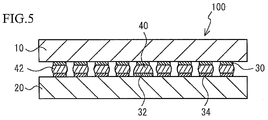
- FIG. 5 is a cross sectional view of a semiconductor device 100 according to the first embodiment.
- the first electrodes 30 each having a circular shape (e.g., a first shape 90 in FIG. 3 ) are formed on the main surface of the first semiconductor chip 10 .
- the second electrode 32 with a cross-like shape e.g., a second shape 92 in FIG. 3
- the third electrodes 34 each with a circular shape which is similar to the first shape 90 surround the periphery of the second electrode 32 .
- the first electrode 30 and the second electrode 32 are bonded via the first solder bump 40 .
- the first electrode 30 and the third electrode 34 are bonded via the second solder bump 42 .
- the first solder bump 40 covers the entire surface of the second electrode 32 .
- the semiconductor device 100 is inspected using an X-ray. Specifically, the bonded portion between the first solder bump 40 and the second electrode 32 is inspected by the X-ray. When the bonded portion is formed satisfactorily, the semiconductor device 100 is determined as acceptable.
- FIG. 6 is a perspective view showing a good bonded portion between the first solder bump 40 and the second electrode 32 .
- the first electrode 30 and the second electrode 32 have different shapes. Accordingly, the upper shape, which is the bonded portion with the first electrode 30 , and the lower shape, which is the bonded portion with the second electrode 32 , of the first solder bump 40 are different.
- the upper shape takes after the first shape 90 which is the same as that of the first electrode 30
- the lower shape takes after the second shape 92 which is the same as that of the second electrode 32 .
- the semiconductor device 100 fails the inspection.
- the inspection regarding the bonded state of the two electrodes can be made by inspecting the shape of the first solder bump 40 even if the images of the two electrodes cannot be obtained by the X-ray. This makes it possible to conduct the X-ray inspection of the bonded portion in quick, simple steps.
- the second shape 92 partially protrudes from the first shape.
- the X-ray inspection is conducted from the direction vertical to the electrode to determine the acceptability of the bonded state based on the shape of the first solder bump 40 .
- the determination with respect to the acceptability of the bonded state may be made based on the state whether or not the entire surface of the second electrode 32 is covered with the first solder bump 40 .
- the semiconductor device is determined as acceptable. In the aforementioned method, only observation of the bonded portion between the first solder bump 40 and the second electrode 32 may be required.
- the second semiconductor chip 20 as the mounted portion includes the second and the third electrodes 32 and 34 each having different shapes.
- the determination with respect to the acceptability of the bonded state may be made based on the state whether or not the first solder bump 40 and the second solder bump 42 bonded to those electrodes have different shapes.
- the electrode image may be vertically picked up by the X-ray for the purpose of confirming the difference in the shape in the fully clarified manner. If the resultant shadings are different, a semiconductor device is determined as acceptable. If the shape of the second electrode 32 and the shape of the third electrode 34 are found to be different, the bonded portion of the semiconductor device 100 passes the test.
- the vertical electrode images obtained by the X-ray may be more simple and quick to analyze the state of the bonded portion. Accordingly, such an X-ray inspection may be conducted immediately after the solder bump bonding step at an early stage of the manufacturing. This may in turn make the manufacturing process of the semiconductor device 100 more productive, less wasteful, and higher yielding.
- FIGS. 7A and 7B illustrate top views of X-ray images of a semiconductor device, according to the second embodiment. Each of FIGS. 7A and 7B shows the image obtained by irradiating the X-ray to the semiconductor device 100 shown in FIG. 5 in the direction vertical to the first and the second electrodes 30 and 32 .
- each of the first and the second electrodes 30 and 32 is as thin as approximately 1 um, a shading 40 x of the first solder bump 40 and a shading 42 x of the second solder bump 42 only appear on the X-ray pick-up image.
- the shape of the shading of the first solder bump 40 in the good bonded state shown in FIG. 7B will be designated as a first reference shape 80 .
- the first reference shape 80 corresponds with the shape derived from superimposing the first shape 90 and the second shape 92 .
- the shading 40 x of the first solder bump 40 is formed to have the cross-shape protruding from the circular shape as shown in FIG. 7B .
- the shape similar to the one shown in FIG. 7B , or the shading of the diagonal image may be used as the first reference shape 80 .
- the shape of the shading 40 x of the first solder bump 40 is compared with the first reference shape 80 . If they are the same, or they are matched with a predetermined matching ratio or higher, the semiconductor device 100 is determined as acceptable.
- the X-ray inspection process according to the second embodiment allows inspection of the bonded state using an X-ray device with a relatively low resolution.
- FIG. 1B is a sectional view of the first semiconductor chip 10 prior to the solder bump bonding.
- FIGS. 8A and 8B illustrate top views of X-ray images of a semiconductor device prior to a solder bump bonding, according to the third embodiment.
- Each of FIGS. 8A and 8B shows the image picked up by irradiating the X-ray to the first semiconductor chip 10 prior to the solder bump bonding in the direction vertical to the first electrode 30 .
- the first electrode 30 is as thin as approximately 1 um, only the shading 48 x of the solder ball 48 may appear on the X-ray pick-up image.
- the shape shown in FIG. 8B is used as a second reference shape 82 .
- the second reference shape 82 corresponds with the shape of the solder ball 48 . That is, as the solder ball 48 is substantially spherical, the resultant shading 48 x becomes circular. The diameter of the shading is the same as that of the solder ball 48 .
- the shape similar to the one shown in FIG. 8B , or the shading of the diagonally picked up image may be used as the second reference shape.
- the shading 40 x of the first solder bump 40 is compared with the second reference shape 82 . If they are different (for example, the cross-shape protrudes from the shading of the solder ball shown in FIG. 7B ), it may be determined as acceptable.
- the data used for the image processing may be less than those for the determination process in the second embodiment.
- the X-ray imaging is performed from a direction vertical to the electrode. However, it is appreciated that the imaging can be performed diagonally or horizontally.
- the fourth embodiment provides a system for manufacturing the semiconductor device illustrated in the first embodiment.
- FIG. 9 is a schematic diagram of an exemplary system 110 for performing and inspecting bonding, according to the fourth embodiment.
- the semiconductor manufacturing system 110 is formed of a solder bump bonding section 50 , an X-ray image pick-up section 60 , and a control unit 70 for controlling the two sections.
- the solder bump bonding section 50 is formed of a flip-chip bonder (not shown).
- the X-ray image pick-up section 60 is formed of an X-ray irradiation unit 62 and an X-ray receiving unit 64 .
- the solder bump bonding section 50 and the X-ray receiving unit 64 are connected to the control unit 70 .
- the X-ray image pick-up section 60 shows the semiconductor device 100 with the first solder bump 40 and the second solder bump 42 .
- the same structures as those in the first and the second embodiments will be designated with the same reference numerals hereinafter.
- the solder bump bonding section 50 bonds the first semiconductor chip 10 provided with the first electrode 30 having the first shape 90 to the second semiconductor chip 20 as the mounted portion provided with the second electrode 32 having the second shape 92 , which is different from the first shape 90 , via the first solder bump 40 .
- the first solder bump 40 is formed from the solder ball 48 on the surface of the first electrode 30 .
- the third electrode 34 provided on the second semiconductor chip 20 as the mounted portion is bonded to the first electrode 30 via the second solder bump 42 .
- the X-ray image pick-up section 60 picks up the X-ray image of the first solder bump 42 .
- the control unit 70 determines the acceptability of the bonded state between the first solder bump 40 and the second electrode 32 based on the image picked up by the X-ray image pick-up section 60 .
- FIG. 10 is a flowchart of an exemplary method for performing and inspecting bonding, according to the fourth embodiment.
- the operation of the semiconductor manufacturing system 110 will be described referring to both FIGS. 9 and 10 .
- the control unit 70 causes the solder bump bonding section 50 to bond the first and the second semiconductor chips 10 and 20 via the first solder bump 40 (not shown) and the second solder bump 42 .
- the semiconductor device 100 according to the first embodiment is completed.
- the control unit 70 allows the conveyance unit (not shown) to convey the semiconductor device 100 to the X-ray image pick-up section 60 .
- step S 14 the control unit 70 causes the X-ray irradiation unit 62 to irradiate an X-ray to the semiconductor device 100 .
- the X-ray which has transmitted through the semiconductor device 100 are received by the X-ray receiving unit 64 , and converted into an electrical signal.
- step S 16 the control unit 70 converts the electric signal received from the X-ray receiving unit 64 into image data.
- step S 18 the control unit 70 modifies the image data to suitable for determining acceptability of the bonding.
- step S 20 the control unit 70 makes the decision as to whether the bonding is acceptable. It is appreciated that the decision may be based on any one of the first to the third embodiments. In the case where the bonded state is satisfactory, the control unit 70 determines that the semiconductor device 100 is acceptable in step S 22 . In the case where the bonded state is not satisfactory, the control unit 70 determines that the semiconductor device 100 is not acceptable in step S 24 .
- the control unit 70 may determine that the semiconductor device 100 is acceptable. In the case where the first solder bump 40 has the shape different from that of the second solder bump 42 , the control unit 70 may determine that the semiconductor device 100 is acceptable. In the case where the shading of the X-ray pick-up image of the first solder bump 40 has the same shape as the first reference shape 80 corresponding to the shape formed by superimposing the first and the second shapes 90 and 92 , the control unit 70 may determine that the semiconductor device 100 is acceptable. In the case where the shading of the X-ray pick-up image of the first solder bump 40 has the shape different from the second reference shape 82 corresponding to the solder ball 48 , the control unit 70 may determine that the semiconductor device 100 is acceptable.
- the shape of the first electrode 30 on the first semiconductor chip 10 is different from that of the second electrode 32 on the second semiconductor chip 20 bonded to the first semiconductor chip 10 by the solder bump bonding section 50 .
- the determination with respect to the acceptability of the bonded state may be made easy by the control unit 70 based on the shading of the X-ray image of the first solder bump 40 picked up by the X-ray image pick-up section 60 .
- the acceptability of the bonded state may be monitored in real time through the control unit 70 . This may make it possible to eliminate defective semiconductor devices from the production line in an early production stage, thus achieving high yield at low cost.
- the second semiconductor chip 20 is employed as the mounted portion.
- an interposer may be employed as the mounted portion where the semiconductor chip is mounted on the interposer through the FCB.
- the electrode When the electrode is formed on the interposer, the electrode may be made thicker (several tens of um) compared with the formation of the electrode on the semiconductor chip. In this case, the X-ray images of both the electrode and the solder bump may be obtained, which makes it possible to determine the acceptability of the bonded state through the generally employed process.
- the determination with respect to the acceptability of the bonded state may be made based on the shape of the solder bump for bonding the first electrode 30 and the second electrode 32 .
- the second electrode 32 has the cross-shaped (e.g., second shape 92 ).
- it may be formed in any shape (e.g., square, rectangular, oval, star, and other shapes) so long as it is different from the shape of the first electrode 30 (e.g., first shape 90 ).
- the second shape 92 at least partially protrudes from the first shape 90 . This makes it possible to confirm the bonded state even by the X-ray image pick-up in the direction vertical to the electrode.
- the surface area of the second electrode 32 is substantially same as that of the third electrode 34 . Supposing that the solder balls each having the same volume are formed on the electrode, it is preferable to make the height of each solder ball equal.
- the respective heights of the first and the second solder bumps 40 and 42 formed from the solder ball 48 become equivalent to the height of the solder bump of the electrode with the larger area. Accordingly, if the electrode area becomes excessively different, the resultant solder bump may be irregularly formed.
- the solder formed of tin and silver is employed as the first solder bump 40 , the second solder bump 42 , and the solder ball 48 .
- solder may be formed using different combinations of metals.
- a combination of tin, silver, and copper or tin and lead may be used as an alloy which turns into a molten state at the predetermined temperature (so as not to damage the loaded components including the first semiconductor chip 10 , for example, 235° C. or lower) to bond the metals.
Landscapes
- Engineering & Computer Science (AREA)
- Microelectronics & Electronic Packaging (AREA)
- Computer Hardware Design (AREA)
- Power Engineering (AREA)
- Manufacturing & Machinery (AREA)
- Physics & Mathematics (AREA)
- Condensed Matter Physics & Semiconductors (AREA)
- General Physics & Mathematics (AREA)
- Analysing Materials By The Use Of Radiation (AREA)
- Wire Bonding (AREA)
Abstract
Description
Claims (20)
Priority Applications (1)
| Application Number | Priority Date | Filing Date | Title |
|---|---|---|---|
| US12/877,661 US8274158B2 (en) | 2007-05-16 | 2010-09-08 | Structure, method and system for assessing bonding of electrodes in FCB packaging |
Applications Claiming Priority (2)
| Application Number | Priority Date | Filing Date | Title |
|---|---|---|---|
| JP2007-130143 | 2007-05-16 | ||
| JP2007130143A JP5350604B2 (en) | 2007-05-16 | 2007-05-16 | Semiconductor device and manufacturing method thereof |
Related Child Applications (1)
| Application Number | Title | Priority Date | Filing Date |
|---|---|---|---|
| US12/877,661 Division US8274158B2 (en) | 2007-05-16 | 2010-09-08 | Structure, method and system for assessing bonding of electrodes in FCB packaging |
Publications (2)
| Publication Number | Publication Date |
|---|---|
| US20080303144A1 US20080303144A1 (en) | 2008-12-11 |
| US7816788B2 true US7816788B2 (en) | 2010-10-19 |
Family
ID=40095090
Family Applications (2)
| Application Number | Title | Priority Date | Filing Date |
|---|---|---|---|
| US12/122,556 Expired - Fee Related US7816788B2 (en) | 2007-05-16 | 2008-05-16 | Structure, method and system for assessing bonding of electrodes in FCB packaging |
| US12/877,661 Active US8274158B2 (en) | 2007-05-16 | 2010-09-08 | Structure, method and system for assessing bonding of electrodes in FCB packaging |
Family Applications After (1)
| Application Number | Title | Priority Date | Filing Date |
|---|---|---|---|
| US12/877,661 Active US8274158B2 (en) | 2007-05-16 | 2010-09-08 | Structure, method and system for assessing bonding of electrodes in FCB packaging |
Country Status (2)
| Country | Link |
|---|---|
| US (2) | US7816788B2 (en) |
| JP (1) | JP5350604B2 (en) |
Cited By (1)
| Publication number | Priority date | Publication date | Assignee | Title |
|---|---|---|---|---|
| US20140183458A1 (en) * | 2013-01-03 | 2014-07-03 | Samsung Display Co., Ltd. | Organic light-emitting display apparatus and method of manufacturing the same |
Families Citing this family (6)
| Publication number | Priority date | Publication date | Assignee | Title |
|---|---|---|---|---|
| JP5263053B2 (en) * | 2009-07-24 | 2013-08-14 | 株式会社村田製作所 | Semiconductor package and semiconductor package module |
| JP5539077B2 (en) | 2010-07-09 | 2014-07-02 | ローム株式会社 | Semiconductor device |
| JP6165411B2 (en) | 2011-12-26 | 2017-07-19 | 富士通株式会社 | Electronic components and electronic equipment |
| US9553040B2 (en) | 2012-03-27 | 2017-01-24 | Mediatek Inc. | Semiconductor package |
| JP5842859B2 (en) * | 2013-04-15 | 2016-01-13 | 株式会社村田製作所 | Multilayer wiring board and module having the same |
| JP2019016678A (en) * | 2017-07-06 | 2019-01-31 | 株式会社フジクラ | Substrate module and method for manufacturing substrate module |
Citations (25)
| Publication number | Priority date | Publication date | Assignee | Title |
|---|---|---|---|---|
| US5062127A (en) * | 1989-05-16 | 1991-10-29 | Mitsubishi Metal Corporation | Metals assay apparatus and method |
| US5214308A (en) * | 1990-01-23 | 1993-05-25 | Sumitomo Electric Industries, Ltd. | Substrate for packaging a semiconductor device |
| US5381307A (en) * | 1992-06-19 | 1995-01-10 | Motorola, Inc. | Self-aligning electrical contact array |
| US5493594A (en) * | 1988-08-26 | 1996-02-20 | Hitachi, Ltd. | Method and apparatus for inspection of solder joints by x-ray fluoroscopic imaging |
| US5641946A (en) * | 1995-07-05 | 1997-06-24 | Anam Industrial Co., Ltd. | Method and circuit board structure for leveling solder balls in ball grid array semiconductor packages |
| US5796169A (en) * | 1996-11-19 | 1998-08-18 | International Business Machines Corporation | Structurally reinforced ball grid array semiconductor package and systems |
| US5811351A (en) * | 1995-12-18 | 1998-09-22 | Matsushita Electric Industrial Co., Ltd. | Semiconductor device and method of manufacturing the same |
| US5828128A (en) * | 1995-08-01 | 1998-10-27 | Fujitsu, Ltd. | Semiconductor device having a bump which is inspected from outside and a circuit board used with such a semiconductor device |
| US5856699A (en) * | 1995-10-20 | 1999-01-05 | Canon Kabushiki Kaisha | Photoelectric conversion apparatus with level photoreceiving surface |
| US5905772A (en) * | 1996-07-08 | 1999-05-18 | U.S. Philips Corporation | X-ray examination apparatus with a semiconductor x-ray detector |
| US6177682B1 (en) * | 1998-10-21 | 2001-01-23 | Novacam Tyechnologies Inc. | Inspection of ball grid arrays (BGA) by using shadow images of the solder balls |
| US6222277B1 (en) * | 1999-06-23 | 2001-04-24 | Emc Corporation | Non-collapsing interconnection for semiconductor devices |
| US6316735B1 (en) * | 1996-11-08 | 2001-11-13 | Ricoh Company, Ltd. | Semiconductor chip mounting board and a semiconductor device using same board |
| US6346679B1 (en) * | 1999-08-27 | 2002-02-12 | Nec Corporation | Substrate on which ball grid array type electrical part is mounted and method for mounting ball grid array type electrical part on substrate |
| US6410861B1 (en) * | 1999-12-03 | 2002-06-25 | Motorola, Inc. | Low profile interconnect structure |
| US6429387B1 (en) * | 1996-12-13 | 2002-08-06 | Matsushita Electric Industrial Co., Ltd. | Electronic component and mounting method and device therefor |
| US6858941B2 (en) * | 2000-12-07 | 2005-02-22 | International Business Machines Corporation | Multi-chip stack and method of fabrication utilizing self-aligning electrical contact array |
| US6927491B1 (en) * | 1998-12-04 | 2005-08-09 | Nec Corporation | Back electrode type electronic part and electronic assembly with the same mounted on printed circuit board |
| US6972494B1 (en) * | 1999-08-17 | 2005-12-06 | Agere Systems Inc. | Integrated circuit die for wire bonding and flip-chip mounting |
| US7084500B2 (en) * | 2003-10-29 | 2006-08-01 | Texas Instruments Incorporated | Semiconductor circuit with multiple contact sizes |
| US7180183B2 (en) * | 2002-10-25 | 2007-02-20 | Siliconware Precision Industries Co., Ltd. | Semiconductor device with reinforced under-support structure and method of fabricating the same |
| US20080018423A1 (en) * | 2005-03-18 | 2008-01-24 | Jun Matsui | Electronic part and circuit substrate |
| US7368806B2 (en) * | 2004-12-14 | 2008-05-06 | Advanced Semiconductor Engineering, Inc. | Flip chip package with anti-floating structure |
| US7564130B1 (en) * | 2007-07-06 | 2009-07-21 | National Semiconductor Corporation | Power micro surface-mount device package |
| US7714452B2 (en) * | 2005-07-05 | 2010-05-11 | International Business Machines Corporation | Structure and method for producing multiple size interconnections |
Family Cites Families (16)
| Publication number | Priority date | Publication date | Assignee | Title |
|---|---|---|---|---|
| JPH0951017A (en) * | 1995-08-04 | 1997-02-18 | Fujitsu Ltd | Semiconductor module |
| US6002172A (en) * | 1997-03-12 | 1999-12-14 | International Business Machines Corporation | Substrate structure and method for improving attachment reliability of semiconductor chips and modules |
| US6271481B1 (en) * | 1998-09-03 | 2001-08-07 | Visteon Global Technologies, Inc. | Pad configurations for improved etching of multilayer circuit assemblies |
| JP2001068836A (en) * | 1999-08-27 | 2001-03-16 | Mitsubishi Electric Corp | Printed wiring board and semicondcutor module, and manufacture thereof |
| JP2001217355A (en) * | 1999-11-25 | 2001-08-10 | Hitachi Ltd | Semiconductor device |
| JP3517388B2 (en) * | 2000-06-14 | 2004-04-12 | 新光電気工業株式会社 | Bump inspection method and bump inspection device |
| JP4341187B2 (en) * | 2001-02-13 | 2009-10-07 | 日本電気株式会社 | Semiconductor device |
| JP3711341B2 (en) * | 2001-04-27 | 2005-11-02 | 沖電気工業株式会社 | Semiconductor device |
| TW555152U (en) * | 2002-12-13 | 2003-09-21 | Advanced Semiconductor Eng | Structure of flip chip package with area bump |
| JP4010244B2 (en) * | 2002-12-20 | 2007-11-21 | ヤマハ株式会社 | Surface mount package |
| TW586199B (en) * | 2002-12-30 | 2004-05-01 | Advanced Semiconductor Eng | Flip-chip package |
| TWI233682B (en) * | 2003-08-22 | 2005-06-01 | Advanced Semiconductor Eng | Flip-chip package, semiconductor chip with bumps, and method for manufacturing semiconductor chip with bumps |
| JP2005209239A (en) * | 2004-01-20 | 2005-08-04 | Nec Electronics Corp | Semiconductor integrated circuit apparatus |
| KR100558066B1 (en) * | 2004-05-14 | 2006-03-10 | 삼성전자주식회사 | Apparatus and Method for Repairing a Metal Bump of Stack Type Semiconductor Devices |
| US7033864B2 (en) * | 2004-09-03 | 2006-04-25 | Texas Instruments Incorporated | Grooved substrates for uniform underfilling solder ball assembled electronic devices |
| US7772104B2 (en) * | 2007-02-02 | 2010-08-10 | Freescale Semiconductor, Inc. | Dynamic pad size to reduce solder fatigue |
-
2007
- 2007-05-16 JP JP2007130143A patent/JP5350604B2/en active Active
-
2008
- 2008-05-16 US US12/122,556 patent/US7816788B2/en not_active Expired - Fee Related
-
2010
- 2010-09-08 US US12/877,661 patent/US8274158B2/en active Active
Patent Citations (25)
| Publication number | Priority date | Publication date | Assignee | Title |
|---|---|---|---|---|
| US5493594A (en) * | 1988-08-26 | 1996-02-20 | Hitachi, Ltd. | Method and apparatus for inspection of solder joints by x-ray fluoroscopic imaging |
| US5062127A (en) * | 1989-05-16 | 1991-10-29 | Mitsubishi Metal Corporation | Metals assay apparatus and method |
| US5214308A (en) * | 1990-01-23 | 1993-05-25 | Sumitomo Electric Industries, Ltd. | Substrate for packaging a semiconductor device |
| US5381307A (en) * | 1992-06-19 | 1995-01-10 | Motorola, Inc. | Self-aligning electrical contact array |
| US5641946A (en) * | 1995-07-05 | 1997-06-24 | Anam Industrial Co., Ltd. | Method and circuit board structure for leveling solder balls in ball grid array semiconductor packages |
| US5828128A (en) * | 1995-08-01 | 1998-10-27 | Fujitsu, Ltd. | Semiconductor device having a bump which is inspected from outside and a circuit board used with such a semiconductor device |
| US5856699A (en) * | 1995-10-20 | 1999-01-05 | Canon Kabushiki Kaisha | Photoelectric conversion apparatus with level photoreceiving surface |
| US5811351A (en) * | 1995-12-18 | 1998-09-22 | Matsushita Electric Industrial Co., Ltd. | Semiconductor device and method of manufacturing the same |
| US5905772A (en) * | 1996-07-08 | 1999-05-18 | U.S. Philips Corporation | X-ray examination apparatus with a semiconductor x-ray detector |
| US6316735B1 (en) * | 1996-11-08 | 2001-11-13 | Ricoh Company, Ltd. | Semiconductor chip mounting board and a semiconductor device using same board |
| US5796169A (en) * | 1996-11-19 | 1998-08-18 | International Business Machines Corporation | Structurally reinforced ball grid array semiconductor package and systems |
| US6429387B1 (en) * | 1996-12-13 | 2002-08-06 | Matsushita Electric Industrial Co., Ltd. | Electronic component and mounting method and device therefor |
| US6177682B1 (en) * | 1998-10-21 | 2001-01-23 | Novacam Tyechnologies Inc. | Inspection of ball grid arrays (BGA) by using shadow images of the solder balls |
| US6927491B1 (en) * | 1998-12-04 | 2005-08-09 | Nec Corporation | Back electrode type electronic part and electronic assembly with the same mounted on printed circuit board |
| US6222277B1 (en) * | 1999-06-23 | 2001-04-24 | Emc Corporation | Non-collapsing interconnection for semiconductor devices |
| US6972494B1 (en) * | 1999-08-17 | 2005-12-06 | Agere Systems Inc. | Integrated circuit die for wire bonding and flip-chip mounting |
| US6346679B1 (en) * | 1999-08-27 | 2002-02-12 | Nec Corporation | Substrate on which ball grid array type electrical part is mounted and method for mounting ball grid array type electrical part on substrate |
| US6410861B1 (en) * | 1999-12-03 | 2002-06-25 | Motorola, Inc. | Low profile interconnect structure |
| US6858941B2 (en) * | 2000-12-07 | 2005-02-22 | International Business Machines Corporation | Multi-chip stack and method of fabrication utilizing self-aligning electrical contact array |
| US7180183B2 (en) * | 2002-10-25 | 2007-02-20 | Siliconware Precision Industries Co., Ltd. | Semiconductor device with reinforced under-support structure and method of fabricating the same |
| US7084500B2 (en) * | 2003-10-29 | 2006-08-01 | Texas Instruments Incorporated | Semiconductor circuit with multiple contact sizes |
| US7368806B2 (en) * | 2004-12-14 | 2008-05-06 | Advanced Semiconductor Engineering, Inc. | Flip chip package with anti-floating structure |
| US20080018423A1 (en) * | 2005-03-18 | 2008-01-24 | Jun Matsui | Electronic part and circuit substrate |
| US7714452B2 (en) * | 2005-07-05 | 2010-05-11 | International Business Machines Corporation | Structure and method for producing multiple size interconnections |
| US7564130B1 (en) * | 2007-07-06 | 2009-07-21 | National Semiconductor Corporation | Power micro surface-mount device package |
Cited By (3)
| Publication number | Priority date | Publication date | Assignee | Title |
|---|---|---|---|---|
| US20140183458A1 (en) * | 2013-01-03 | 2014-07-03 | Samsung Display Co., Ltd. | Organic light-emitting display apparatus and method of manufacturing the same |
| US9627656B2 (en) * | 2013-01-03 | 2017-04-18 | Samsung Display Co., Ltd. | Organic light-emitting display apparatus and method of manufacturing the same |
| US10593906B2 (en) | 2013-01-03 | 2020-03-17 | Samsung Display Co., Ltd. | Organic light-emitting display apparatus and method of manufacturing the same |
Also Published As
| Publication number | Publication date |
|---|---|
| JP2008288297A (en) | 2008-11-27 |
| US20080303144A1 (en) | 2008-12-11 |
| US8274158B2 (en) | 2012-09-25 |
| JP5350604B2 (en) | 2013-11-27 |
| US20110057309A1 (en) | 2011-03-10 |
Similar Documents
| Publication | Publication Date | Title |
|---|---|---|
| US8274158B2 (en) | Structure, method and system for assessing bonding of electrodes in FCB packaging | |
| TWI607537B (en) | Semiconductor apparatus | |
| US20060278998A1 (en) | Integrated electronic chip and interconnect device and process for making the same | |
| JP5656144B2 (en) | Method of joining metal members | |
| US7679188B2 (en) | Semiconductor device having a bump formed over an electrode pad | |
| Sikka et al. | Direct bonded heterogeneous integration (DBHi) Si bridge | |
| US9035442B2 (en) | Semiconductor module | |
| US6400034B1 (en) | Semiconductor device | |
| Lannon et al. | High density metal–metal interconnect bonding for 3-D integration | |
| Sakuma et al. | Differential heating/cooling chip joining method to prevent chip package interaction issue in large die with ultra low-k technology | |
| CN106463427B (en) | Semiconductor device and method for manufacturing the same | |
| CN108573885B (en) | Semiconductor device, manufacturing method thereof and electronic device | |
| Gagnon et al. | Thermo-compression bonding and mass reflow assembly processes of 3D logic die stacks | |
| US8492171B2 (en) | Techniques and structures for testing integrated circuits in flip-chip assemblies | |
| US8716868B2 (en) | Semiconductor module for stacking and stacked semiconductor module | |
| CN106971945B (en) | Semiconductor device, manufacturing method thereof and electronic device | |
| US9601424B2 (en) | Interposer and methods of forming and testing an interposer | |
| CN110870071B (en) | Image forming apparatus and method of manufacturing the same | |
| Daily et al. | Microscrubbing: An alternative method for 3D thermocompression bonding CuCu bumps and high bump density devices with low force, time and temperature | |
| CN101488482B (en) | Semi-conductor package structure and manufacturing method thereof | |
| TW201042751A (en) | Semiconductor module for stacking and stacked semiconductor module | |
| US20230351577A1 (en) | Automatic optical inspection system and method | |
| JP2023065027A (en) | Semiconductor light receiving element, method of manufacturing the same, and method of inspecting the same | |
| TWI387079B (en) | Semiconductor package structure and method for manufacturing the same | |
| Kada et al. | Dream Chip Project at ASET |
Legal Events
| Date | Code | Title | Description |
|---|---|---|---|
| AS | Assignment |
Owner name: SPANSION LLC, CALIFORNIA Free format text: ASSIGNMENT OF ASSIGNORS INTEREST;ASSIGNORS:KASAI, JUNICHI;TANAKA, JUNJI;MASUDA, NAOMI;REEL/FRAME:021431/0565;SIGNING DATES FROM 20080726 TO 20080804 Owner name: SPANSION LLC, CALIFORNIA Free format text: ASSIGNMENT OF ASSIGNORS INTEREST;ASSIGNORS:KASAI, JUNICHI;TANAKA, JUNJI;MASUDA, NAOMI;SIGNING DATES FROM 20080726 TO 20080804;REEL/FRAME:021431/0565 |
|
| AS | Assignment |
Owner name: BARCLAYS BANK PLC,NEW YORK Free format text: SECURITY AGREEMENT;ASSIGNORS:SPANSION LLC;SPANSION INC.;SPANSION TECHNOLOGY INC.;AND OTHERS;REEL/FRAME:024522/0338 Effective date: 20100510 Owner name: BARCLAYS BANK PLC, NEW YORK Free format text: SECURITY AGREEMENT;ASSIGNORS:SPANSION LLC;SPANSION INC.;SPANSION TECHNOLOGY INC.;AND OTHERS;REEL/FRAME:024522/0338 Effective date: 20100510 |
|
| FPAY | Fee payment |
Year of fee payment: 4 |
|
| AS | Assignment |
Owner name: SPANSION LLC, CALIFORNIA Free format text: RELEASE BY SECURED PARTY;ASSIGNOR:BARCLAYS BANK PLC;REEL/FRAME:035201/0159 Effective date: 20150312 Owner name: SPANSION TECHNOLOGY LLC, CALIFORNIA Free format text: RELEASE BY SECURED PARTY;ASSIGNOR:BARCLAYS BANK PLC;REEL/FRAME:035201/0159 Effective date: 20150312 Owner name: SPANSION INC., CALIFORNIA Free format text: RELEASE BY SECURED PARTY;ASSIGNOR:BARCLAYS BANK PLC;REEL/FRAME:035201/0159 Effective date: 20150312 |
|
| AS | Assignment |
Owner name: MORGAN STANLEY SENIOR FUNDING, INC., NEW YORK Free format text: SECURITY INTEREST;ASSIGNORS:CYPRESS SEMICONDUCTOR CORPORATION;SPANSION LLC;REEL/FRAME:035240/0429 Effective date: 20150312 |
|
| AS | Assignment |
Owner name: CYPRESS SEMICONDUCTOR CORPORATION, CALIFORNIA Free format text: ASSIGNMENT OF ASSIGNORS INTEREST;ASSIGNOR:SPANSION, LLC;REEL/FRAME:036042/0212 Effective date: 20150601 |
|
| AS | Assignment |
Owner name: CYPRESS SEMICONDUCTOR CORPORATION, CALIFORNIA Free format text: PARTIAL RELEASE OF SECURITY INTEREST IN PATENTS;ASSIGNOR:MORGAN STANLEY SENIOR FUNDING, INC., AS COLLATERAL AGENT;REEL/FRAME:039708/0001 Effective date: 20160811 Owner name: SPANSION LLC, CALIFORNIA Free format text: PARTIAL RELEASE OF SECURITY INTEREST IN PATENTS;ASSIGNOR:MORGAN STANLEY SENIOR FUNDING, INC., AS COLLATERAL AGENT;REEL/FRAME:039708/0001 Effective date: 20160811 |
|
| FEPP | Fee payment procedure |
Free format text: PAYER NUMBER DE-ASSIGNED (ORIGINAL EVENT CODE: RMPN); ENTITY STATUS OF PATENT OWNER: LARGE ENTITY Free format text: PAYOR NUMBER ASSIGNED (ORIGINAL EVENT CODE: ASPN); ENTITY STATUS OF PATENT OWNER: LARGE ENTITY |
|
| AS | Assignment |
Owner name: MONTEREY RESEARCH, LLC, CALIFORNIA Free format text: ASSIGNMENT OF ASSIGNORS INTEREST;ASSIGNOR:CYPRESS SEMICONDUCTOR CORPORATION;REEL/FRAME:040911/0238 Effective date: 20160811 |
|
| FEPP | Fee payment procedure |
Free format text: MAINTENANCE FEE REMINDER MAILED (ORIGINAL EVENT CODE: REM.) |
|
| LAPS | Lapse for failure to pay maintenance fees |
Free format text: PATENT EXPIRED FOR FAILURE TO PAY MAINTENANCE FEES (ORIGINAL EVENT CODE: EXP.); ENTITY STATUS OF PATENT OWNER: LARGE ENTITY |
|
| STCH | Information on status: patent discontinuation |
Free format text: PATENT EXPIRED DUE TO NONPAYMENT OF MAINTENANCE FEES UNDER 37 CFR 1.362 |
|
| FP | Lapsed due to failure to pay maintenance fee |
Effective date: 20181019 |
|
| AS | Assignment |
Owner name: MORGAN STANLEY SENIOR FUNDING, INC., NEW YORK Free format text: CORRECTIVE ASSIGNMENT TO CORRECT THE 8647899 PREVIOUSLY RECORDED ON REEL 035240 FRAME 0429. ASSIGNOR(S) HEREBY CONFIRMS THE SECURITY INTERST;ASSIGNORS:CYPRESS SEMICONDUCTOR CORPORATION;SPANSION LLC;REEL/FRAME:058002/0470 Effective date: 20150312 |