US7800365B2 - Magnetic detection device and electrical product - Google Patents
Magnetic detection device and electrical product Download PDFInfo
- Publication number
- US7800365B2 US7800365B2 US12/623,029 US62302909A US7800365B2 US 7800365 B2 US7800365 B2 US 7800365B2 US 62302909 A US62302909 A US 62302909A US 7800365 B2 US7800365 B2 US 7800365B2
- Authority
- US
- United States
- Prior art keywords
- magnetic field
- magnetic
- output
- detection device
- detection signal
- Prior art date
- Legal status (The legal status is an assumption and is not a legal conclusion. Google has not performed a legal analysis and makes no representation as to the accuracy of the status listed.)
- Active
Links
Images


Classifications
-
- G—PHYSICS
- G01—MEASURING; TESTING
- G01R—MEASURING ELECTRIC VARIABLES; MEASURING MAGNETIC VARIABLES
- G01R33/00—Arrangements or instruments for measuring magnetic variables
- G01R33/02—Measuring direction or magnitude of magnetic fields or magnetic flux
- G01R33/06—Measuring direction or magnitude of magnetic fields or magnetic flux using galvano-magnetic devices
- G01R33/09—Magnetoresistive devices
- G01R33/093—Magnetoresistive devices using multilayer structures, e.g. giant magnetoresistance sensors
-
- B—PERFORMING OPERATIONS; TRANSPORTING
- B82—NANOTECHNOLOGY
- B82Y—SPECIFIC USES OR APPLICATIONS OF NANOSTRUCTURES; MEASUREMENT OR ANALYSIS OF NANOSTRUCTURES; MANUFACTURE OR TREATMENT OF NANOSTRUCTURES
- B82Y25/00—Nanomagnetism, e.g. magnetoimpedance, anisotropic magnetoresistance, giant magnetoresistance or tunneling magnetoresistance
Definitions
- the present invention relates to a magnetic detection device which is capable of conducting bipolar detection, and particularly, to a magnetic detection device capable of switching among plural output modes, and an electrical product using the magnetic detection device.
- a magnetic detection device (magnetic sensor) provided with a magnetoresistive effect element may be employed for detecting open/close state of an electrical product such as a folding mobile phone and a refrigerator.
- the electric resistance value of the magnetoresistive effect element changes in accordance with the external magnetic field intensity. It is therefore possible to detect intensity level of the external magnetic field applied to the magnetic detection device based on the voltage change resulting from the resistance change.
- the magnetic detection device is controlled in one of output modes including a bipolar 2-output mode for detecting bipolar of the external magnetic field in (+) direction and the external magnetic field in ( ⁇ ) direction opposite the (+) direction to output a (+) magnetic field detection signal and a ( ⁇ ) magnetic field detection signal from the respective output terminals, a bipolar 1-output mode for detecting the bipolar as described above to output the (+) magnetic field detection signal and the ( ⁇ ) magnetic field detection signal from a common output terminal, and a single-pole 1-output mode for detecting only one of the external magnetic fields in (+) direction and ( ⁇ ) direction to output one of the (+) magnetic field detection signal and the ( ⁇ ) magnetic field detection signal.
- the desired output mode may differ.
- the aforementioned three output modes cannot be obtained from the single magnetic detection device.
- the magnetic detection devices each for the different output mode have to be manufactured separately, resulting in the cost increase.
- Patent Documents such as Japanese Unexamined Patent Application Publication Nos. 2000-180206, 59-5976, and 2004-180286 does not disclose the structure which allows the common magnetic detection device to provide the three output modes as described above.
- the present invention provides a magnetic detection device capable of easily switching among plural output modes, and an electrical product using the magnetic detection device.
- the present invention provides a magnetic detection device provided with a sensor unit which changes an electrical characteristic in accordance with change in each magnetic field intensity of external magnetic fields in (+) direction and ( ⁇ ) direction opposite the (+) direction, and an integrated circuit which is connected to the sensor unit for generating and outputting a (+) magnetic field detection signal and a ( ⁇ ) magnetic field detection signal based on the change in the electrical characteristic.
- the integrated circuit is provided with two output terminals and a mode switch circuit which includes a pair of switch terminals.
- the mode switch circuit is capable of switching between a 1-output mode for outputting the (+) and ( ⁇ ) magnetic field detection signals from one of the output terminals and a 2-output mode for outputting the (+) magnetic field detection signal from the one of the output terminal and the ( ⁇ ) magnetic field detection signal from the other output terminal, respectively depending on a shortcircuit state or a non-shortcircuit state between the switch terminals.
- the shortcircuit state and the non-shortcircuit state are allowed to be externally adjusted.
- the magnetic detection device is capable of switching the output mode between 1-output mode and 2-output mode, which may eliminate the need of manufacturing different magnetic detection devices for providing the respective output modes.
- the output mode may be switched by externally adjusting the switch terminal into shortcircuit state or non-shortcircuit state, resulting in easy switching of the output mode.
- the switch terminal is exposed on a surface of the device, and is adjusted into the shortcircuit state or the non-shortcircuit state based on an electrically coupled state or an electrically decoupled state between the switch terminals.
- an operation member having a surface opposite the switch terminals formed of a conductive material is exposed on the surface of the device, and operated to adjust the switch terminals into the shortcircuit state via the operation member or the non-shortcircuit state having the operation member apart from the switch terminals.
- the sensor unit includes a first circuit for detecting a (+) magnetic field, which is provided with a first magnetoresistive effect element using a magnetoresistive effect having an electric resistance changed based on the change in the magnetic field intensity of the external magnetic field in the (+) direction, and a second circuit for detecting a ( ⁇ ) magnetic field, which is provided with a second magnetoresistive effect element using the magnetoresistive effect having the electric resistance changed based on the change in the magnetic field intensity of the external magnetic field in the ( ⁇ ) direction.
- the sensor unit may be appropriately formed to be adapted to the bipolar detection.
- the present invention provides an electrical product which contains the magnetic detection device as described above, which is formed to have one of a structure in which the magnetic detection device is adjusted to the 1-output mode, and an output terminal for outputting the (+) magnetic field detection signal and the ( ⁇ ) magnetic field detection signal is connected to a circuit substrate in the product, a structure in which the magnetic detection device is adjusted to the 2-output mode, and an output terminal for outputting the (+) magnetic field detection signal and the output terminal for outputting the ( ⁇ ) magnetic field detection signal are connected to the circuit substrate of the product, and a structure in which the magnetic detection device is adjusted to the 2-output mode, and only one of the output terminals for outputting the (+) magnetic field detection signal and the ( ⁇ ) magnetic field detection signal is connected to the circuit substrate in the product.
- the electrical product is allowed to be operated in the desired output mode selectable from the bipolar 1-output mode, the bipolar 2-output mode, and the single-pole 1-output mode using the single magnetic detection device.
- the magnetic detection device is structured to switch between the 1-output mode and 2-output mode, thus eliminating the need of manufacturing the magnetic detection devices for providing the respective output modes.
- the output mode switching operation may be performed by externally adjusting the switch terminal into the shortcircuit state or the non-shortcircuit state. This makes it possible to easily switch the output mode.
- the single magnetic detection device as described above is built in the electrical product so as to be easily operated in the desired output mode selectable from the bipolar 1-output mode, the bipolar 2-output mode, and the single-pole 1-output mode using the single magnetic detection device.
- FIG. 1 is an entire circuit diagram showing a structure of a magnetic detection device according to an embodiment
- FIG. 2 is a plan view illustrating the magnetic detection device installed in the electrical product in an output mode
- FIG. 3 is a plan view illustrating the magnetic detection device installed in the electrical product in another output mode
- FIG. 4 is a plan view illustrating the magnetic detection device installed in the electrical product in another output mode
- FIG. 5 is a plan view illustrating the magnetic detection device installed in the electrical product in an output mode with the structure different from those shown in FIGS. 2 to 4 ;
- FIG. 6 is a plan view illustrating the magnetic detection device installed in the electrical product in the output mode with the structure different from those shown in FIGS. 2 to 4 ;
- FIG. 7 is a partially sectional view illustrating each layer structure of a first magnetoresistive effect element, a second magnetoresistive effect element, a first fixed resistance element and a second fixed resistance element;
- FIG. 8 is a graph for explaining a curve R-H of the first magnetoresistive effect element
- FIG. 9 is a graph for explaining a curve R-H of the second magnetoresistive effect element
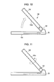
- FIG. 10 is an explanatory view of an embodiment with respect to usage of the magnetic detection device of the embodiment (partially illustrating a folding mobile phone which contains the magnetic detection device in an opened state);
- FIG. 11 is an explanatory view of an embodiment with respect to usage of the magnetic detection device of the embodiment (partially illustrating the folding mobile phone which contains the magnetic detection device while having the first member turned over);
- FIG. 12 is an explanatory view of an embodiment with respect to usage of the magnetic detection device of the embodiment (plan view partially illustrating the folding mobile phone which contains the magnetic detection device as illustrated in FIG. 10 );
- FIG. 13 is an explanatory view of an embodiment with respect to usage of the magnetic detection device of the embodiment (plan view partially illustrating the folding mobile phone which contains the magnetic detection device as illustrated in FIG. 11 ).
- FIG. 1 is an entire circuit diagram illustrating a magnetic detection device 20 according to an embodiment.
- FIGS. 2 to 6 are plan views each showing the magnetic detection device 20 of the embodiment installed in the electrical product in the respective output modes.
- FIG. 7 is a sectional view partially illustrating each layer structure of a first magnetoresistive effect element, a second magnetoresistive effect element, a first fixed resistance element and a second fixed resistance element according to the embodiment.
- FIG. 8 illustrates a curve R-H of the first magnetoresistive effect element.
- FIG. 9 illustrates a curve R-H of the second magnetoresistive effect element.
- FIGS. 10 and 11 are sectional views each illustrating a folding mobile phone having the magnetic detection device installed therein as examples for explaining usage of the magnetic detection device of the embodiment.
- FIGS. 12 and 13 are plan views each illustrating the folding mobile phone.
- the magnetic detection device 20 of the embodiment shown in FIG. 1 includes a sensor unit 21 and an integrated circuit (IC) 22 .
- IC integrated circuit
- the sensor unit 21 includes a first series circuit 26 having a first magnetoresistive effect element 23 and a first fixed resistance element 24 connected in series via a first output extraction unit 25 , and a second series circuit 30 having a second magnetoresistive effect element 27 and a second fixed resistance element 28 connected in series via a second output extraction unit 29 .
- the integrated circuit 22 is provided with a third series circuit 34 having a third fixed resistance element 31 and a fourth fixed resistance element 32 connected in series via a third output extraction unit 33 .
- the third series circuit 34 forms bridge circuits with the first series circuit 26 and the second series circuit 30 as a common circuit.
- first bridge circuit first circuit unit
- second bridge circuit second circuit unit
- the first magnetoresistive effect element 23 is connected to the fourth fixed resistance element 32 in parallel, and the first fixed resistance element 24 is connected to the third fixed resistance element 31 in parallel.
- the second magnetoresistive effect element 27 is connected to the third fixed resistance element 31 in parallel, and the second fixed resistance element 28 is connected to the fourth fixed resistance element 32 in parallel.
- the integrated circuit 22 is provided with an input terminal (power source) 39 , a ground terminal 42 , and two external output terminals 40 and 41 .
- the integrated circuit 22 is provided with a single differential amplifier 35 to which the third output extraction unit 33 of the third series circuit 34 is connected.
- first output extraction unit 25 of the first series circuit 26 and the second output extraction unit 29 of the second series circuit 30 are connected to an input unit of a switch circuit 36 , respectively.
- An output unit of the switch circuit 36 is connected to an input unit of the differential amplifier 35 .
- an output unit of the differential amplifier 35 is connected to a comparator 38 of Schmitt trigger type, and an output unit of the comparator 38 is further connected to a first latch circuit 46 and a second latch circuit 47 .
- Output units of the latch circuits 46 and 47 are connected to the first external output terminal 40 and the second external output terminal 41 , respectively.
- a mode switch circuit 50 is interposed between the latch circuits 46 , 47 and the external output terminals 40 , 41 .
- the integrated circuit 22 is provided with a not shown clock circuit.
- the clock signal from the clock circuit is time divided into a first clock signal (Sig T+) and a second clock signal (Sig T ⁇ ) at a considerably short cycle so as to be input into the respective switch circuits 36 , 55 , the latch circuits 46 , 47 , and a threshold control circuit 56 .
- the first output extraction unit 25 When the first clock signal (Sig T+) is input, the first output extraction unit 25 is connected to the differential amplifier 35 via the switch circuit 36 , and the first bridge circuit is connected to the ground terminal 42 via the switch circuit 55 .
- the first clock signal (Sig T+) is input to the first latch circuit 46 such that a magnetic field detection signal ((+) magnetic field detection signal) generated based on the change in the electric characteristic of the first bridge circuit is retained in the first latch circuit 46 .
- the second output extraction unit 29 When the second clock signal (Sig T ⁇ ) is input, the second output extraction unit 29 is connected to the differential amplifier 35 via the switch circuit 36 , and the second bridge circuit is connected to the ground terminal 42 via the switch circuit 55 .
- the second clock signal (Sig T ⁇ ) is input to the second latch circuit 46 such that the magnetic field signal (( ⁇ ) magnetic field detection signal) generated based on the change in the electric characteristic in the second bridge circuit is retained in the second latch circuit 47 .
- the (+) magnetic field detection signal is a detection signal corresponding to the change in the magnetic field intensity of the external magnetic field H in (+) direction.
- such signal is controlled to be generated when the differential potential from the differential amplifier 35 based on the change in the magnetic field intensity of the external magnetic field H in (+) direction exceeds a predetermined threshold level generated in case of the first clock signal (Sig T+) in the threshold control circuit 56 .
- the ( ⁇ ) magnetic field detection signal is a detection signal corresponding to the change in the magnetic field intensity of the external magnetic field H in ( ⁇ ) direction.
- such signal is controlled to be generated when the differential potential from the differential amplifier 35 based on the change in the magnetic field intensity of the external magnetic field H in ( ⁇ ) direction exceeds the predetermined threshold level generated in case of the second clock signal (Sig T ⁇ ) in the threshold control circuit 56 .
- the magnetic detection device 20 of the embodiment is capable of generating both the (+) and ( ⁇ ) magnetic field detection signals.
- the mode switch circuit 50 shown in FIG. 1 is formed of a function control circuit 57 which includes a logic circuit, and a pair of switch terminals 58 , 59 .
- FIG. 2 illustrates the external output terminals 40 , 41 , and the switch terminals 58 , 59 .
- FIG. 2 illustrates the first magnetoresistive effect element 23 , the second magnetoresistive effect element 27 , the first fixed resistance element 24 and the second fixed resistance element 28 .
- those elements are formed on the surface of the magnetic detection device 20 in a meander form.
- the input terminal 39 and the ground terminal 42 are exposed on the surface of the magnetic detection device 20 although they are not shown in FIG. 2 .
- the switch terminals 58 and 59 are in the non-shortcircuit state.
- the mode switch circuit 50 allows both the (+) magnetic field detection signal and ( ⁇ ) magnetic field detection signal to be output from the first external output terminal 40 .
- the ( ⁇ ) magnetic field detection signal is output from the second external output terminal 41 as well.
- a first input terminal 61 on a circuit substrate 60 in the electrical product and the first external output terminal 40 are electrically coupled through wire bonding, for example so as to operate the electrical product in the bipolar 1-output mode.
- each change in the magnetic field intensity of the external magnetic fields H both in (+) and ( ⁇ ) directions may be detected.
- both the magnetic field detection signals are output only from the external output terminal 40 .
- the direction of the external magnetic field H cannot be detected.
- the switch terminals 58 and 59 are in the shortcircuit state.
- the switch terminals 58 and 59 are electrically coupled through a known method such as wire bonding, soldering and plating.
- the switch terminals 58 and 59 are brought into the shortcircuit state such that the mode switch circuit 50 allows the (+) magnetic field detection signal to be output from the first external output element 40 , and the ( ⁇ ) magnetic field detection signal to be output from the second external output terminal 41 , respectively.
- the first input terminal 61 on the circuit substrate 60 in the electrical product and the first external output terminal 40 are electrically coupled through the wire bonding, and a second input terminal 62 and the second external output terminal 41 are electrically coupled through the wire bonding.
- each change in the magnetic field intensity of the external magnetic field in (+) and ( ⁇ ) directions may be detected, and (+) and ( ⁇ ) magnetic field detection signals may be output from the respective external output terminals 40 and 41 , separately. This makes it possible to detect the direction of the external magnetic field H.
- the switch terminals 58 and 59 are brought into the shortcircuit state to allow the magnetic detection device 20 capable of outputting the (+) magnetic field detection signal from the first external output terminal 40 , and the ( ⁇ ) magnetic field detection signal from the second external output terminal 41 to be installed in the electrical product as shown in FIG. 4 .
- the electrical product may be operated in the single-pole 1-output mode in the case where the first external output terminal 40 is only coupled with the first input terminal 61 in the electrical product, and the second external output terminal 41 and the second input terminal 62 are not electrically coupled.
- the change in the magnetic field intensity of any one of the external magnetic fields H in the (+) direction and the ( ⁇ ) direction may only be detected.
- the switch terminals 58 and 59 are in the non-shortcircuit state as shown in FIG. 2 .
- the first external output terminal 40 and the first input terminal 61 in the electrical product may be electrically coupled as shown in FIG. 2 .
- the switch terminals 58 and 59 are brought into the shortcircuit state, and the external output terminal and the input terminal in the product are electrically coupled before or after installation of the magnetic detection device 20 in the electrical product.
- the magnetic detection device 20 In the initial state, the magnetic detection device 20 according to the embodiment may be manufactured while having the switch terminals 58 and 59 brought into the shortcircuit state as shown in FIGS. 3 and 4 . At this time, in the case where the magnetic detection device 20 is installed in the electrical product to be used in the bipolar 2-output mode or the single-pole 1-output mode, the external output terminal and the first input terminal in the product may be electrically coupled as shown in FIGS. 3 and 4 .
- the shortcircuit state between the switch terminals 58 and 59 is cut into the non-shortcircuit state, and the first external output terminal 40 and the first input terminal 61 in the product are electrically coupled. If the switch terminals 58 and 59 are electrically coupled with wire, the wire may be cut using tool.
- the mode switch circuit 50 serves to adjust both the (+) magnetic field detection signal and ( ⁇ ) magnetic field detection signal to be output from the first external output terminal 40 (1-output mode).
- the mode switch circuit 50 serves to adjust the (+) magnetic field detection signal to be output from the first external output terminal 40 , and the ( ⁇ ) magnetic field detection signal to be output from the second external output terminal 41 , respectively (2-output mode).
- the mode switch circuit 50 may be operated to adjust the (+) magnetic field detection signal to be output from the first external output terminal 40 , and the ( ⁇ ) magnetic field detection signal to be output from the second external output terminal 41 , respectively (2-output mode) when the switch terminals 58 and 59 are in the non-shortcircuit state, and the (+) magnetic field detection signal and the ( ⁇ ) magnetic field detection signal to be output from the first external output terminal 40 (1-output mode) when the switch terminals 58 and 59 are in the shortcircuit state by changing the logic circuit for forming the mode switch circuit 50 .
- the mode in the initial state, when the magnetic detection device 20 according to the embodiment is manufactured while having the switch terminals 58 and 59 held in the shortcircuit state, the mode is set to the 1-output mode.
- the first external output terminal 40 and the first input terminal 61 in the electrical product are electrically coupled for operating the electrical product in the bipolar 1-output mode likewise the case shown in FIG. 2 .
- the electric coupling between the switch terminals 58 and 59 is cut into the non-shortcircuit state, and the external output terminal and the input terminal in the product are electrically coupled to allow the electrical product to be operated in the bipolar 2-output mode or the single-pole 1-output mode in the same way as in the cases shown in FIGS. 3 and 4 .
- the mode is set to the 2-output mode as described above. Then the external output terminal and the input terminal in the product are electrically coupled likewise the cases shown in FIGS. 3 and 4 to allow the electrical product to be operated in the bipolar 2-output mode or the single-pole 1-output mode.
- the switch terminals 58 and 59 are brought into the shortcircuit state, and the first external output terminal 40 and the first input terminal 61 in the product are electrically coupled to allow the electrical product to be operated in the bipolar 1-output mode likewise the case shown in FIG. 2 .
- FIGS. 2 to 4 the switch terminals 58 and 59 are brought into the shortcircuit state through the wire bonding, and the non-shortcircuit state through the wire cutting.
- a metal slide member (operation member) 70 with at least the surface opposite the switch terminals 58 and 59 slidable in the arrangement direction thereof may be provided as shown in FIG. 5 so as to easily adjust the shortcircuit state or the non-shortcircuit state between the switch terminals 58 and 59 via the slide member 70 .
- FIG. 5 illustrates the non-shortcircuit state between the switch terminals 58 and 59
- FIG. 6 illustrates the shortcircuit state between the switch terminals 58 and 59 .
- a press button (operation member) may be provided on the switch terminals 58 and 59 .
- the switch terminals 58 and 59 are brought into the shortcircuit state via the button.
- the switch terminals 58 and 59 are brought into the non-shortcircuit state.
- the structure provided with the operation member on the switch terminals 58 and 59 allows the shortcircuit state and the non-shortcircuit state between the switch terminals 58 and 59 to be easily switched frequently.
- the operation member may be exposed on the surface of the electrical product to allow user of the electrical product to easily operate the operation member.
- the user is further allowed to arbitrarily select from the plural modes for operating the product.
- the integrated circuit 22 is provided with the mode switch circuit 50 which includes two external output terminals 40 and 41 , and a pair of the switch terminals 58 and 59 , and is allowed to switch the output mode between the 1-output mode for outputting the (+) and ( ⁇ ) magnetic field detection signals from the first external output terminal 40 , and the 2-output mode for outputting the (+) and ( ⁇ ) magnetic field detection signals from the first external output terminal 40 and the second external output terminal 41 , respectively depending on the shortcircuit state or the non-shortcircuit state between the switch terminals 58 and 59 .
- the switch terminals 58 and 59 are exposed on the surface of the device as shown in FIGS. 2 to 4 so as to allow the shortcircuit state and the non-shortcircuit state to be externally adjusted.
- the magnetic detection device 20 is allowed to switch between the 1-output mode and the 2-output mode, and accordingly, individual magnetic detection devices for providing the respective output modes do not have to be produced.
- the output mode may be switched by adjusting the shortcircuit state or the non-shortcircuit state between the switch terminals 58 and 59 externally, thus allowing the output mode to be easily switched.
- the electrical product is allowed to be operated in any one of the bipolar 1-output mode, the bipolar 2-output mode, and the single-pole 1-output mode.
- the magnetic detection devices adapted to the respective output modes required for the electrical product do not have to be produced.
- the magnetic detection device 20 may be commonly used, thus reducing the manufacturing cost compared with the case of the generally employed magnetic detection device.
- FIG. 7 is a sectional view illustrating each cross section of the first magnetoresistive effect element 23 , the second magnetoresistive effect element 27 , the first fixed resistance element 24 , and the second fixed resistance element 28 which are assumed to be arranged in-line on the same substrate 80 .
- each of the first magnetoresistive effect element 23 and the second magnetoresistive effect element 27 has a base layer 81 , an antiferromagnetic layer 82 , a fixed magnetic layer 83 , a nonmagnetic material layer 84 , a free magnetic layer 85 and a protection layer 86 sequentially laminated from the bottom.
- the base layer 81 is formed of a nonmagnetic material which is selected as one or two kinds from the group including Ta, Hf, Nb, Zr, Ti, Mo and W.
- the antiferromagnetic layer 82 is formed of the antiferromagnetic material which contains an element ⁇ ( ⁇ is one or two kinds selected from the group including Pt, Pd, It, Rh, Ru and Os) and Mn, or the antiferromagnetic material which contains the elements ⁇ and ⁇ ′ ( ⁇ ′ is the element as one or two kinds selected from the group including Ne, Ar, Kr, Xe, Be, B, C, N, Mg, Al, Si, P, Ti, V, Cr, Fe, Co, Ni, Cu, Zn, Ga, Ge, Zr, Nb, Mo, Ag, Cd, Sn, Hf, Ta, W, Re, Au, Pb and rare-earth element) and Mn.
- the antiferromagnetic layer 82 is formed of IrMn or PtMn.
- Each of the fixed magnetic layer 83 and the free magnetic layer 85 is formed of the magnetic material such as CoFe alloy, NiFe alloy and CoFeNi alloy.
- the nonmagnetic material layer 84 is formed of the nonmagnetic metal material, for example.
- the nonmagnetic material layer 84 is formed of Cu.
- the protection layer 86 is formed of Ta and the like.
- the fixed magnetic layer 83 and the free magnetic layer 85 may have a laminated ferri structure (laminated structure of magnetic layer/nonmagnetic intermediate layer/magnetic layer having magnetic directions of two magnetic layers which interpose the nonmagnetic layer directed antiparallel).
- Each of the fixed magnetic layer 83 and the free magnetic layer 85 may have the laminated structure formed of different plural magnetic layers.
- the layer structure may be formed by laminating the base layer 80 , the free magnetic layer 85 , the nonmagnetic material layer 84 , the fixed magnetic layer 83 , the antiferromagnetic layer 82 and the protection layer 86 from the bottom.
- Each of the first magnetoresistive effect element 23 and the second magnetoresistive effect element 27 has the antiferromagnetic layer 82 and the fixed magnetic layer 83 formed in contact with each other. Then the thermal process is performed in the magnetic field to form an exchange coupled magnetic field (Hex) on the interface between the antiferromagnetic layer 82 and the fixed magnetic layer 83 so as to fix the magnetizing direction of the fixed magnetic layer 83 to one direction.
- a magnetizing direction 83 a of the fixed magnetic layer 83 is shown by an arrow direction.
- Each magnetizing direction 83 a of the fixed magnetic layer 83 of the first magnetoresistive effect element 23 and the second magnetoresistive effect element 27 is indicated by X2 direction.
- the magnetizing direction of the free magnetic layer 85 in a zero-magnetic field state is different between the first magnetoresistive effect element 23 and the second magnetoresistive effect element 27 .
- a magnetizing direction 85 a of the free magnetic layer 85 of the first magnetoresistive effect element 23 is indicated by the X2 direction which is the same as the magnetizing direction 83 a of the fixed magnetic layer 83 .
- the magnetizing direction 85 b of the free magnetic layer 85 of the second magnetoresistive effect element 27 is indicated by X1 direction which is antiparallel with respect to the magnetizing direction 83 a of the fixed magnetic layer 83 .
- FIG. 8 illustrates the curve R-H of the first magnetoresistive effect element 23 .
- the external magnetic field H is gradually intensified from the zero-magnetic field state (no external magnetic field) toward the (+) direction, the parallel state between the magnetizing direction 85 a of the free magnetic layer 85 and the magnetizing direction 83 a of the fixed magnetic layer 83 collapses to approximate to the antiparallel state.
- the resistance value R of the first magnetoresistive effect element 23 gradually increases along a curve HR 1 .
- the resistance value R of the first magnetoresistive effect element 23 is gradually decreased along a curve HR 2 .
- the curve R-H of the first magnetoresistive effect element 23 forms a loop L 1 defined by the curves HR 1 and HR 2 in accordance with intensity change of the external magnetic field H in the (+) direction.
- the center value of the expanded width of the loop L 1 as the intermediate value between the maximum and the minimum resistance values of the first magnetoresistive effect element 23 is a “midpoint” of the loop L 1 .
- the intensity of the magnetic field at the midpoint of the loop L 1 determines magnitude of a first interlayer coupling magnetic field Hin 1 applied between the free magnetic layer 85 and the fixed magnetic layer 83 . Referring to FIG. 8 , the first interlayer coupling magnetic field Hin 1 of the first magnetoresistive effect element 23 shifts toward the (+) external magnetic field direction.
- the magnetizing direction 85 a of the free magnetic layer 85 of the first magnetoresistive effect element 23 does not fluctuate, but the magnetizing direction 85 b of the free magnetic layer 85 of the second magnetoresistive effect element 27 fluctuates to change the resistance value thereof.
- FIG. 9 illustrates the curve R-H of the second magnetoresistive effect element 27 .
- the external magnetic field H is gradually intensified from the zero-magnetic field state (no external magnetic field applied) to the ( ⁇ ) direction
- the antiparallel state between the magnetizing direction 85 b of the free magnetic layer 85 and the magnetizing direction 83 a of the fixed magnetic layer 83 collapses to approximate to the parallel state.
- the resistance value R of the second magnetoresistive effect element 27 gradually decreases along a curve HR 3 .
- the resistance value R of the second magnetoresistive effect element 27 is gradually increased along a curve HR 4 .
- the curve R-H of the second magnetoresistive effect element 27 forms a loop L 2 defined by the curves HR 3 and HR 4 in accordance with the intensity change of the external magnetic field in the ( ⁇ ) direction.
- the center value of the expanded width of the loop L 2 as the intermediate value between the maximum and the minimum resistance values of the second magnetoresistive effect element 27 is a “midpoint” of the loop L 2 .
- the intensity of the magnetic field at the midpoint of the loop L 2 determines the magnitude of a second interlayer coupling magnetic field Hin 2 applied between the free magnetic layer 85 and the fixed magnetic layer 83 . Referring to FIG. 9 , the second interlayer coupling magnetic field Hin 2 of the second magnetoresistive effect element 27 shifts toward the ( ⁇ ) external magnetic field direction.
- the first interlayer coupling magnetic field Hin 1 is the positive value
- the second interlayer coupling magnetic field Hin 2 is a negative value. In this way, the first and the second interlayer coupling magnetic fields Hin 1 and Hin 2 are reversely coded with positive/negative values.
- Each material composition of the first magnetoresistive effect element 23 and the second magnetoresistive effect element 27 is made the same to set each TCR of those elements 23 and 27 to be substantially the same.
- the film thickness of the nonmagnetic material layer 84 formed of Cu is made different between the first magnetoresistive effect element 23 and the second magnetoresistive effect element 27 to adjust the first interlayer coupling magnetic field Hin 1 to the positive value and the second interlayer coupling magnetic field Hin 2 to the negative value.
- the film structure of the first fixed resistance element 24 connected to the first magnetoresistive effect element 23 in series is the same as that of the second fixed resistance element 28 connected to the second magnetoresistive effect element 27 in series.
- each material composition of the first fixed resistance element 24 and the second fixed resistance element 28 is the same as that of the first magnetoresistive effect element 23 and the second magnetoresistive effect element 27 .
- the magnetic layer 87 and the nonmagnetic material layer 88 corresponding to the free magnetic layer 85 are inversely laminated.
- each of the first and the second fixed resistance elements 24 and 28 has the base layer 81 , the antiferromagnetic layer 82 , the fixed magnetic layer 83 , the magnetic layer 87 , the nonmagnetic material layer 88 and the protection layer 86 sequentially laminated from the bottom.
- Each of the first and the second fixed resistance elements 24 and 28 has the fixed magnetic layer 83 and the magnetic layer 87 sequentially laminated on the antiferromagnetic layer 82 .
- Magnetization of the fixed magnetic layer 83 and the magnetic layer 87 may be fixed by exchange coupling magnetic field (Hex) generated with the antiferromagnetic layer 82 , and ferromagnetic coupling between the fixed magnetic layer 83 and the magnetic layer 87 .
- the magnetic layer 87 formed of the same material as that of the free magnetic layer 85 in the magnetoresistive effect elements 23 and 27 does not fluctuate the magnetization to the external magnetic field unlike the free magnetic layer 85 thereof.
- Each electric resistance value of the first fixed resistance element 24 and the second fixed resistance element 28 is not fluctuated by the external magnetic field.
- the first fixed resistance element 24 and the second fixed resistance element 28 may have the single layer structure formed of the same material rather than the laminated structure as shown in FIG. 7 .
- the magnetic detection device 20 of bipolar detection type is installed in a folding mobile phone 100 of turn-over type.
- the magnetic detection device 20 detects opening of the mobile phone 100 in response to the intensity change in the external magnetic field applied to the magnetic detection device 20 .
- the folding mobile phone 100 includes a first member 102 with a display screen and a second member 103 with an operation surface.
- a magnet 101 is positioned as illustrated by a plan view of FIG. 12 .
- the external magnetic field H in the (+) direction is applied from the magnet 101 to the magnetic detection device 20 .
- the folding mobile phone 100 is closed from the state shown in FIG. 10 , the external magnetic field H in the (+) direction applied to the magnetic detection device 20 is gradually intensified. Then the differential potential exceeds the threshold level to generate the (+) magnetic detection signal, based on which the closing of the folding mobile phone 100 is detected.
- the first member 102 of the mobile phone 100 is turned around the rotating axis at 180°.
- a screen display 102 a which has been an inner surface of the first member 102 is exposed as the outer surface shown in FIGS. 11 and 13 .
- the direction of the magnet 101 is inverted from the arrangement state shown in FIG. 12 .
- the external magnetic field H in the ( ⁇ ) direction is applied from the magnet 101 to the magnetic detection device 20 .
- the folding mobile phone 100 is closed from the state shown in FIG. 11
- the external magnetic field H in the ( ⁇ ) direction applied to the magnetic detection device 20 is gradually intensified.
- the differential potential exceeds the threshold level to generate the ( ⁇ ) magnetic field detection signal, based on which the closing of the folding type mobile phone 100 is detected.
- the (+) and ( ⁇ ) magnetic detection signals may be obtained and output separately. It may be determined whether or not the first member 102 is turned over when opening/closing the mobile phone. In the case where the folding mobile phone 100 is opened/closed without turning over the first member 102 as shown in FIGS. 10 and 12 , turning ON/OFF of the backlight of the display screen upon the opening/closing is controlled. As shown in FIGS. 11 and 13 , in the case where the first member 102 is turned over to open/close the folding mobile phone 100 , the function other than the normal opening/closing detection, for example, the camera function may be activated.
- the turn-over/non-turn-over of the first member 102 cannot be detected.
- the opening/closing detection may be enabled, thus improving workability of the assembly.
- the TMR element tunnel type magnetoresistive effect element
- the AMR element isotropic magnetoresistive effect element
- the hall element may be employed.
Abstract
Description
Claims (5)
Applications Claiming Priority (3)
| Application Number | Priority Date | Filing Date | Title |
|---|---|---|---|
| JP2007153695 | 2007-06-11 | ||
| JP2007-153695 | 2007-06-11 | ||
| PCT/JP2008/060558 WO2008153004A1 (en) | 2007-06-11 | 2008-06-09 | Magnetic detection device and electric product |
Related Parent Applications (1)
| Application Number | Title | Priority Date | Filing Date |
|---|---|---|---|
| PCT/JP2008/060558 Continuation WO2008153004A1 (en) | 2007-06-11 | 2008-06-09 | Magnetic detection device and electric product |
Publications (2)
| Publication Number | Publication Date |
|---|---|
| US20100066359A1 US20100066359A1 (en) | 2010-03-18 |
| US7800365B2 true US7800365B2 (en) | 2010-09-21 |
Family
ID=40129609
Family Applications (1)
| Application Number | Title | Priority Date | Filing Date |
|---|---|---|---|
| US12/623,029 Active US7800365B2 (en) | 2007-06-11 | 2009-11-20 | Magnetic detection device and electrical product |
Country Status (4)
| Country | Link |
|---|---|
| US (1) | US7800365B2 (en) |
| EP (1) | EP2159587B1 (en) |
| JP (1) | JP5048771B2 (en) |
| WO (1) | WO2008153004A1 (en) |
Families Citing this family (2)
| Publication number | Priority date | Publication date | Assignee | Title |
|---|---|---|---|---|
| JP5634041B2 (en) * | 2009-02-17 | 2014-12-03 | ローム株式会社 | Magnetic sensor and electronic device equipped with the same |
| CN104065367B (en) * | 2013-03-20 | 2017-11-07 | 江苏多维科技有限公司 | A kind of low-watt consumption magnetic resistance switch sensor |
Citations (9)
| Publication number | Priority date | Publication date | Assignee | Title |
|---|---|---|---|---|
| US4628259A (en) | 1980-09-29 | 1986-12-09 | Hitachi, Ltd. | Magneto resistive sensor for detecting movement of a rotating body |
| US4677380A (en) | 1982-06-16 | 1987-06-30 | Lgz Landis | Magnetic field sensor comprising two component layer transistor of opposite polarities |
| JP2000180206A (en) | 1998-12-21 | 2000-06-30 | Mitsubishi Electric Corp | Magnetism detecting device |
| US6100680A (en) * | 1996-01-17 | 2000-08-08 | Allegro Microsystems, Inc. | Detecting the passing of magnetic articles using a transducer-signal detector having a switchable dual-mode threshold |
| US6242908B1 (en) * | 1996-01-17 | 2001-06-05 | Allegro Microsystems, Inc. | Detection of passing magnetic articles while adapting the detection threshold |
| JP2003014834A (en) | 2001-07-03 | 2003-01-15 | Koganei Corp | Magnetic detection sensor |
| JP2003262665A (en) | 2002-03-08 | 2003-09-19 | Asahi Kasei Electronics Co Ltd | Magnetometric sensor |
| JP2004180286A (en) | 2002-11-13 | 2004-06-24 | Matsushita Electric Ind Co Ltd | Magnetic field sensor, magnetic field detecting apparatus, and magnetic field detecting method |
| US20090174401A1 (en) * | 2007-12-26 | 2009-07-09 | Kabushiki Kaisha Toshiba | Magnetic detection circuit |
Family Cites Families (2)
| Publication number | Priority date | Publication date | Assignee | Title |
|---|---|---|---|---|
| JPS5760262A (en) * | 1980-09-29 | 1982-04-12 | Hitachi Ltd | Rotary detector for rotary object |
| US6356741B1 (en) * | 1998-09-18 | 2002-03-12 | Allegro Microsystems, Inc. | Magnetic pole insensitive switch circuit |
-
2008
- 2008-06-09 EP EP08765348.1A patent/EP2159587B1/en active Active
- 2008-06-09 WO PCT/JP2008/060558 patent/WO2008153004A1/en active Application Filing
- 2008-06-09 JP JP2009519250A patent/JP5048771B2/en active Active
-
2009
- 2009-11-20 US US12/623,029 patent/US7800365B2/en active Active
Patent Citations (9)
| Publication number | Priority date | Publication date | Assignee | Title |
|---|---|---|---|---|
| US4628259A (en) | 1980-09-29 | 1986-12-09 | Hitachi, Ltd. | Magneto resistive sensor for detecting movement of a rotating body |
| US4677380A (en) | 1982-06-16 | 1987-06-30 | Lgz Landis | Magnetic field sensor comprising two component layer transistor of opposite polarities |
| US6100680A (en) * | 1996-01-17 | 2000-08-08 | Allegro Microsystems, Inc. | Detecting the passing of magnetic articles using a transducer-signal detector having a switchable dual-mode threshold |
| US6242908B1 (en) * | 1996-01-17 | 2001-06-05 | Allegro Microsystems, Inc. | Detection of passing magnetic articles while adapting the detection threshold |
| JP2000180206A (en) | 1998-12-21 | 2000-06-30 | Mitsubishi Electric Corp | Magnetism detecting device |
| JP2003014834A (en) | 2001-07-03 | 2003-01-15 | Koganei Corp | Magnetic detection sensor |
| JP2003262665A (en) | 2002-03-08 | 2003-09-19 | Asahi Kasei Electronics Co Ltd | Magnetometric sensor |
| JP2004180286A (en) | 2002-11-13 | 2004-06-24 | Matsushita Electric Ind Co Ltd | Magnetic field sensor, magnetic field detecting apparatus, and magnetic field detecting method |
| US20090174401A1 (en) * | 2007-12-26 | 2009-07-09 | Kabushiki Kaisha Toshiba | Magnetic detection circuit |
Also Published As
| Publication number | Publication date |
|---|---|
| US20100066359A1 (en) | 2010-03-18 |
| JPWO2008153004A1 (en) | 2010-08-26 |
| EP2159587A1 (en) | 2010-03-03 |
| EP2159587B1 (en) | 2020-03-11 |
| WO2008153004A1 (en) | 2008-12-18 |
| JP5048771B2 (en) | 2012-10-17 |
| EP2159587A4 (en) | 2017-11-15 |
Similar Documents
| Publication | Publication Date | Title |
|---|---|---|
| JP4810275B2 (en) | Magnetic switch | |
| US7402998B2 (en) | Magnetic detection device including circuit capable of switching over output mode of N pole and S pole between non-separated one output and separated two outputs | |
| JP5066524B2 (en) | Magnetic detector | |
| JP4668818B2 (en) | Magnetic sensor | |
| JP2008134181A (en) | Magnetic detector and its manufacturing method | |
| JP4904352B2 (en) | Magnetic sensor | |
| WO2008059914A1 (en) | Magnetic detector and electronic apparatus employing it | |
| JP4904358B2 (en) | Magnetic detector | |
| US7800365B2 (en) | Magnetic detection device and electrical product | |
| JP2007271319A (en) | Magnetic sensor, and manufacturing method therefor | |
| JP5006339B2 (en) | Magnetic detector | |
| EP2645118A1 (en) | Magnetic detecting element and magnetic sensor utilizing same | |
| EP2088446B1 (en) | Magnetic detector and electronic device | |
| JP5015966B2 (en) | Magnetic detection device and manufacturing method thereof | |
| JP5184380B2 (en) | Magnetic detector | |
| WO2019065690A1 (en) | Exchange coupled film, and magnetoresistance effect element and magnetism detection device using same | |
| JP5184379B2 (en) | Magnetic detector | |
| JP2010190571A (en) | Magnetic detector |
Legal Events
| Date | Code | Title | Description |
|---|---|---|---|
| AS | Assignment |
Owner name: ALPS ELECTRIC CO., LTD.,JAPAN Free format text: ASSIGNMENT OF ASSIGNORS INTEREST;ASSIGNORS:SATO, KIYOSHI;ANDO, HIDETO;GOCHOU, HIDEKI;REEL/FRAME:023551/0880 Effective date: 20091117 Owner name: ALPS ELECTRIC CO., LTD., JAPAN Free format text: ASSIGNMENT OF ASSIGNORS INTEREST;ASSIGNORS:SATO, KIYOSHI;ANDO, HIDETO;GOCHOU, HIDEKI;REEL/FRAME:023551/0880 Effective date: 20091117 |
|
| STCF | Information on status: patent grant |
Free format text: PATENTED CASE |
|
| FPAY | Fee payment |
Year of fee payment: 4 |
|
| FEPP | Fee payment procedure |
Free format text: PAYOR NUMBER ASSIGNED (ORIGINAL EVENT CODE: ASPN); ENTITY STATUS OF PATENT OWNER: LARGE ENTITY |
|
| MAFP | Maintenance fee payment |
Free format text: PAYMENT OF MAINTENANCE FEE, 8TH YEAR, LARGE ENTITY (ORIGINAL EVENT CODE: M1552) Year of fee payment: 8 |
|
| AS | Assignment |
Owner name: ALPS ALPINE CO., LTD., JAPAN Free format text: CHANGE OF NAME;ASSIGNOR:ALPS ELECTRIC CO., LTD.;REEL/FRAME:048209/0197 Effective date: 20190101 |
|
| MAFP | Maintenance fee payment |
Free format text: PAYMENT OF MAINTENANCE FEE, 12TH YEAR, LARGE ENTITY (ORIGINAL EVENT CODE: M1553); ENTITY STATUS OF PATENT OWNER: LARGE ENTITY Year of fee payment: 12 |