US7747177B2 - Coherent phase-shift-keying - Google Patents
Coherent phase-shift-keying Download PDFInfo
- Publication number
- US7747177B2 US7747177B2 US11/204,607 US20460705A US7747177B2 US 7747177 B2 US7747177 B2 US 7747177B2 US 20460705 A US20460705 A US 20460705A US 7747177 B2 US7747177 B2 US 7747177B2
- Authority
- US
- United States
- Prior art keywords
- optical
- digital
- digital signals
- optical carrier
- signals
- Prior art date
- Legal status (The legal status is an assumption and is not a legal conclusion. Google has not performed a legal analysis and makes no representation as to the accuracy of the status listed.)
- Expired - Fee Related, expires
Links
Images


Classifications
-
- H—ELECTRICITY
- H04—ELECTRIC COMMUNICATION TECHNIQUE
- H04L—TRANSMISSION OF DIGITAL INFORMATION, e.g. TELEGRAPHIC COMMUNICATION
- H04L27/00—Modulated-carrier systems
- H04L27/18—Phase-modulated carrier systems, i.e. using phase-shift keying
- H04L27/22—Demodulator circuits; Receiver circuits
-
- H—ELECTRICITY
- H04—ELECTRIC COMMUNICATION TECHNIQUE
- H04L—TRANSMISSION OF DIGITAL INFORMATION, e.g. TELEGRAPHIC COMMUNICATION
- H04L27/00—Modulated-carrier systems
- H04L27/18—Phase-modulated carrier systems, i.e. using phase-shift keying
- H04L27/22—Demodulator circuits; Receiver circuits
- H04L27/223—Demodulation in the optical domain
-
- H—ELECTRICITY
- H04—ELECTRIC COMMUNICATION TECHNIQUE
- H04B—TRANSMISSION
- H04B10/00—Transmission systems employing electromagnetic waves other than radio-waves, e.g. infrared, visible or ultraviolet light, or employing corpuscular radiation, e.g. quantum communication
- H04B10/60—Receivers
-
- H—ELECTRICITY
- H04—ELECTRIC COMMUNICATION TECHNIQUE
- H04B—TRANSMISSION
- H04B10/00—Transmission systems employing electromagnetic waves other than radio-waves, e.g. infrared, visible or ultraviolet light, or employing corpuscular radiation, e.g. quantum communication
- H04B10/60—Receivers
- H04B10/61—Coherent receivers
- H04B10/616—Details of the electronic signal processing in coherent optical receivers
- H04B10/6164—Estimation or correction of the frequency offset between the received optical signal and the optical local oscillator
-
- H—ELECTRICITY
- H04—ELECTRIC COMMUNICATION TECHNIQUE
- H04B—TRANSMISSION
- H04B10/00—Transmission systems employing electromagnetic waves other than radio-waves, e.g. infrared, visible or ultraviolet light, or employing corpuscular radiation, e.g. quantum communication
- H04B10/60—Receivers
- H04B10/61—Coherent receivers
- H04B10/616—Details of the electronic signal processing in coherent optical receivers
- H04B10/6165—Estimation of the phase of the received optical signal, phase error estimation or phase error correction
-
- H—ELECTRICITY
- H04—ELECTRIC COMMUNICATION TECHNIQUE
- H04B—TRANSMISSION
- H04B10/00—Transmission systems employing electromagnetic waves other than radio-waves, e.g. infrared, visible or ultraviolet light, or employing corpuscular radiation, e.g. quantum communication
- H04B10/60—Receivers
- H04B10/61—Coherent receivers
- H04B10/63—Homodyne, i.e. coherent receivers where the local oscillator is locked in frequency and phase to the carrier signal
-
- H—ELECTRICITY
- H04—ELECTRIC COMMUNICATION TECHNIQUE
- H04L—TRANSMISSION OF DIGITAL INFORMATION, e.g. TELEGRAPHIC COMMUNICATION
- H04L27/00—Modulated-carrier systems
- H04L27/18—Phase-modulated carrier systems, i.e. using phase-shift keying
- H04L27/22—Demodulator circuits; Receiver circuits
- H04L27/227—Demodulator circuits; Receiver circuits using coherent demodulation
-
- H—ELECTRICITY
- H04—ELECTRIC COMMUNICATION TECHNIQUE
- H04L—TRANSMISSION OF DIGITAL INFORMATION, e.g. TELEGRAPHIC COMMUNICATION
- H04L27/00—Modulated-carrier systems
- H04L27/0014—Carrier regulation
- H04L2027/0024—Carrier regulation at the receiver end
- H04L2027/0026—Correction of carrier offset
- H04L2027/003—Correction of carrier offset at baseband only
Definitions
- the invention relates to coherent detection methods for phase-shifting-keying and apparatus for performing such methods.
- Quadrature phase-shift-keying is a more bandwidth-efficient modulation scheme than simple on-off modulation schemes.
- QPSK receivers typically have an analog phase lock loop (PLL) for providing the type of coherent detection typically needed to implement a QPSK modulation scheme.
- PLL phase lock loop
- the PLL provides feedback that enables phase and frequency tracking of the transmitted optical carrier by a local oscillator.
- the local oscillator provides a reference signal for down mixing of the modulated carrier wave received from the transmitter.
- the optical receiver has a local optical oscillator for down mixing the received modulated optical carrier and also has an optical PLL.
- the optical PLL feeds back information for phase and frequency synchronizing the local optical oscillator to the optical carrier.
- optical PLLs are often difficult to achieve.
- conventional laser sources often have large line widths.
- the large line widths can make optical phase synchronization difficult at data transmission rates.
- an absence of efficient and inexpensive apparatus for implementing such synchronization has hindered the development of coherent optical communications systems that could otherwise more efficiently use the available optical bandwidth.
- various embodiments of optical detectors herein digitally perform the synchronization needed for coherent detection in phase-shift keying (PSK) modulation schemes. Instead of rigid phase and frequency locking of the local light source to the received modulated optical carrier, these optical detectors have a digital module that effectively provides for such phase and frequency synchronization.
- PSK phase-shift keying
- the invention provides a receiver for coherent detection of a PSK modulated optical carrier.
- the receiver includes an optical detector, digital-to-analog converters, and a digital module.
- the optical detector is configured to mix the modulated optical carrier with two phase components of a reference optical carrier and to produce analog output signals representative of optical signals produced by said mixing.
- the digital-to-analog converters are connected to receive the analog output signals and to produce digital signals from the received analog output signals.
- the digital module is connected to receive the digital signals and to perform one of compensating the received digital signals for a conjugate phase misalignment between the mixed components, extracting phases of the received digital signals, and estimating a frequency offset between the two carriers from the received digital signals.
- the invention provides a method.
- the method includes mixing a PSK modulated optical carrier with first and second phase components of a reference optical carrier and producing electrical signals that measure intensities of optical signals formed by the mixing.
- the method also includes digitalizing the electrical signals to produce a series of digital signals, evaluating derivatives of phases of the digital signals, and decoding the PSK modulated optical carrier based on the evaluated derivatives.
- the invention features an apparatus that includes a digital module.
- the digital module is configured to evaluate a sequence of PSK symbols that modulates a received carrier by decoding a stream of digital signals produced by down mixing the carrier with a reference carrier.
- the digital module is configured to perform one of compensating the digital signals for conjugate phase misalignment during the down mixing, extracting phases of the digital signals, and estimating a frequency offset between the modulated carrier and the reference carrier from the digital signals.
- FIG. 1A shows a constellation of signal points for binary phase-shift keying (BPSK);
- FIG. 1B shows a constellation of signal points for quadrature phase-shift keying (QPSK);
- FIG. 1C shows a constellation of signal points for 8 phase-shift keying (8PSK);
- FIG. 1D shows a constellation of signal points for 16 phase-shift-keying (16PSK);
- FIG. 2 is a block diagram for an exemplary embodiment of an optical receiver that is configured for coherent detection of a phase-shift-keying (PSK) modulated optical carrier in differential encoding;
- PSK phase-shift-keying
- FIG. 3 is a block diagram illustrating a specific embodiment of an optical detector in one embodiment of the optical receiver of FIG. 2 ;
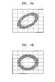
- FIG. 4A shows a computer-simulated distribution of QPSK modulation values after distortion due to conjugate phase misalignment, frequency offset, and noise;
- FIG. 4B shows a computer simulated distribution of QPSK modulation values of FIG. 4A after compensation to remove an averaged conjugate phase misalignment
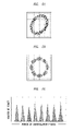
- FIG. 5A shows a computer-simulated distribution of QPSK signal values in the presence of a frequency offset and noise
- FIG. 5B shows a computer simulation of the QPSK signal points of FIG. 5A after compensation to remove a time-averaged frequency offset
- FIG. 5C shows a computer-simulated distribution of 8PSK modulation values after distortion due to conjugate phase misalignment, frequency offset, and noise;
- FIG. 5D shows a computer simulated distribution of the 8PSK modulation values of FIG. 5C after compensation to remove an average conjugate phase misalignment and an average frequency offset;
- FIG. 5E shows a computer-simulated distribution of phases of 8PSK modulation values in the presence of noise and a frequency offset
- FIG. 6 illustrates a method of operating an optical receiver that provides for coherent detection of a PSK modulated optical carrier in differential coding
- FIG. 7A shows an exemplary embodiment of the digital module (DM) of the optical receivers in FIGS. 2 and 3 ;
- FIG. 7B shows an alternate exemplary embodiment of the DM of the optical receivers in FIGS. 2 and 3 in which compensation of conjugate phase misalignment is not performed digitally.
- FIGS. 1A-1D illustrate the signal points, i.e., symbols, of various types of phase-shift keying (PSK).
- FIG. 1A shows a binary PSK (BPSK) constellation in which the two signal points 0 and 1 lie on the unit circle at the azimuthal angles of 0 and ⁇ , respectively.
- FIG. 1B shows a quadrature PSK (QPSK) constellation in which the four signal points 0 , 1 , 2 , and 3 lie on the unit circle at the azimuthal angles of 0, ⁇ /2, ⁇ , and 3 ⁇ /2, respectively.
- BPSK binary PSK
- QPSK quadrature PSK
- FIGS. 1A-1D arrows illustrate motions of the PSK signal points in differential coding.
- BPSK, QPSK, 8PSK, and 16PSK one symbol encodes 1, 2, 3, and 4 bits, respectively.
- the arrows include labels for the multi-bit sets encoded by various motions between the signal points of the underlying BPSK, QPSK, 8PSK, and 16PSK of FIGS. 1A-1D .
- the motion of QPSK signal point 0 into respective QPSK signal points 0 , 1 , 2 , and 3 may be, e.g., differentially encoded by bit pairs 01, 00, 10, and 11.
- various types of optical transmitters encode data according to one of the PSK schemes, e.g., a PSK scheme of FIGS. 1A-1D in differential coding.
- various embodiments of the optical receiver 10 also decode the modulated optical carrier according to the same PSK scheme, e.g., one of the PSK schemes of FIGS. 1A-1D via a differential technique.
- FIG. 2 shows an example of an optical receiver 10 that is configured to perform coherent differential detection of a PSK modulated optical carrier, e.g., an optical carrier modulated according to one of the PSK schemes of FIGS. 1A-1D .
- the optical receiver 10 includes a local optical oscillator 12 ; a 2 ⁇ 2 optical detector 14 ; differential amplifiers 16 A- 16 B; digital-to-analog (D/A) converters 18 A, 18 B; and a digital module (DM) 20 .
- DM digital module
- the local optical oscillator 12 transmits a continuous-wave (CW) reference optical carrier to optical input B of the 2 ⁇ 2 optical detector 14 .
- the other optical input A of the 2 ⁇ 2 optical detector 14 receives a PSK modulated optical carrier from the optical transmitter 6 via an optical transmission channel 8 .
- the optical transmission channel 8 may be a free space channel or an optical fiber line.
- the local optical oscillator 12 may be, e.g., a CW coherent light source such as a diode laser.
- the CW reference optical carrier down mixes the PSK modulated optical carrier in the 2 ⁇ 2 optical detector 14 .
- the local optical oscillator 12 is designed to generate a reference optical carrier whose frequency, ⁇ LO , is approximately equal to the frequency, ⁇ OC , of the PSK modulated optical carrier from the optical transmitter 6 .
- the optical receiver 10 does not have an optical phase lock loop (PLL) that tightly locks the phase and frequency of reference optical carrier from the local optical oscillator 12 to the frequency of the PSK modulated optical carrier from the optical transmitter 6 .
- PLL optical phase lock loop
- line widths of light from the local optical oscillator 12 and the optical transmitter 6 typically produce frequency variations that would be sufficient to destroy such a tight optical synchronization.
- the reference optical carrier of the local optical oscillator 12 will generally have both a phase offset, ⁇ n , and a frequency offset, i.e., ⁇ LO ⁇ OC , with respect to the PSK modulated optical carrier received at the optical input A.
- the frequency offset should slowly drift in time due to line width variations in both optical sources.
- the 2 ⁇ 2 optical detector 14 receives the PSK modulated optical carrier and the CW reference optical carrier at its optical inputs A, B. From these optical carriers, the 2 ⁇ 2 optical detector generates analog electrical signals at a first pair of electrical outputs C and a second pair of electrical outputs D.
- the differential amplifiers 16 A and 16 B convert these electrical signals into analog voltages V 1 and V 2 that carry information corresponding to the PSK phase modulation on the optical carrier received at optical input A.
- the 2 ⁇ 2 electro-optical detector 14 and differential amplifier 16 A are configured to produce an analog output voltage V 1 of the form A′ cos( ⁇ S + ⁇ n +t[ ⁇ OC ⁇ LO ]), and the 2 ⁇ 2 electro-optical detector 14 and differential amplifier 16 B are configured to produce an analog output voltage V 2 of the form A′ sin( ⁇ + ⁇ S + ⁇ n +t[ ⁇ OC ⁇ OL ]).
- ⁇ S has the desired PSK phase modulation information
- ⁇ n is a phase offset between the PSK modulated optical carrier and the CW reference optical carrier
- ⁇ is the conjugate phase misalignment.
- the ⁇ S 's take values in the PSK constellation being transmitted by the optical transmitter 6 and detected by the optical receiver 10 .
- the variable ⁇ S will take values in the sets ⁇ 0, ⁇ , ⁇ 0, ⁇ /2, ⁇ , 3 ⁇ /2 ⁇ , ⁇ 0. ⁇ /4, ⁇ /2, 3 ⁇ /4, ⁇ , 5 ⁇ /4, 3 ⁇ /2, 7 ⁇ /4 ⁇ , and ⁇ S
- the conjugate phase misalignment is the difference between ⁇ /2 and the relative difference between the phases of the reference optical carriers mixed with the received optical carrier in the optical mixers 32 A and 32 B.
- the conjugate phase misalignment is an angle in radians that is defined modulo 2 ⁇ . In particular, there is no conjugate phase misalignment if the components of the reference optical carrier mix with the modulated optical carrier with a relative phase difference of ⁇ /2 in the optical mixers 32 A and 32 B.
- FIG. 3 shows an exemplary embodiment of the optical detector 14 of FIG. 2 .
- the optical detector 14 may be, e.g., fabricated using conventional silicon optical bench technology, e.g., on a crystalline silicon substrate.
- the optical detector 14 includes optical splitters 30 ; 2 ⁇ 2 optical mixers 32 A, 32 B; optical waveguides 34 , 36 ; optical delay 38 ; and balanced pairs of photodiodes 40 .
- the optical splitters 30 e.g., transmit one polarization component of the received light to each optical output 31 .
- the optical outputs 31 of the optical splitters 30 connect via optical waveguides 34 , 36 to the optical mixers 32 A, 32 B.
- the two optical mixers 32 A, 32 B coherently mix light received at their optical inputs to produce selected combinations at their optical outputs. Indeed, each optical mixer 32 A, 32 B is constructed so that the difference between intensities of the selected combinations on the optical outputs of the optical mixer 32 A, 32 B has one of the above cosine and sine forms.
- the optical mixers 32 A, 32 B may be, e.g., conventional multi-mode interference (MMI) devices.
- MMI multi-mode interference
- a pair of balanced photodiodes 40 functions as a detector for light transmit to the optical outputs of the optical mixer 32 A, 32 B.
- either the optical delay 38 and/or the waveguides 34 , 36 produce a relative phase delay between conjugate components of the reference optical carrier.
- conjugate components refer to two components of the reference optical carrier that are delivered to optical mixers 32 A and 32 B.
- the relative phase delay is equal to ⁇ /2+ ⁇ , i.e., up to additions of 2 ⁇ times an integer.
- the small angle ⁇ is an undesired conjugate phase misalignment between the components input to the optical mixers 32 A and 32 B.
- a nonzero conjugate phase misalignment angle would be expected as a result of limits on manufacturing tolerances.
- the A/D converters 18 A, 18 B digitalize the analog voltages V 1 and V 2 of the A/D converters 18 A, 18 B into a sequence of complex digital signals, Y(k).
- Y(k) Y 1 (k)+Y 2 (k)
- “k” indexes the sampling time at the A/D converters 18 A, 18 B.
- the digital components Y 1 (k) and Y 2 (k) satisfy a digitalized form of the above cosine and sine equations on the respective analog voltages V 1 and V 2 .
- “T” represents the sampling period in the A/D converters 18 A, 18 B and “k” is an integer variable to enumerate the time, i.e., 1, 2, 3, etc.
- the A/D converters 18 A, 18 B transmit the sequence of complex digital signals, i.e., the series ⁇ Y(k) ⁇ , to the DM 20 .
- the DM 20 processes the sequence of complex digital signals, Y(k), to reduce or remove undesired physical distortions and then, decodes the resulting processed signals.
- the processing reduces physical distortions associated with optical line widths, the optical phase offset, the optical frequency offset, and optionally the conjugate phase misalignment between the relative phases of the components of the reference optical carrier that are mixed with the received optical carrier. Absent such corrections, these physical distortions could cause systematic errors during decoding of the sequence of complex digital signals ⁇ Y(n) ⁇ .
- the decoding step recovers a sequence estimates, i.e., ⁇ X(n) ⁇ , corresponding to the sequence bit groups, i.e., ⁇ x(n) ⁇ , of the PSK signal points that have been modulated onto the optical carrier received at the optical input A.
- the various physical distortions affect the values of the complex digital signals, i.e., the Y(k)'s.
- Several of these physical distortions are compensated or corrected in the DM 20 of FIGS. 2-3 . That is, the analog distortions generated via optical transmission and analog optical detection are compensated or corrected in the digital domain rather than in the analog domain itself. For that reason, the optical receiver 10 does not need an optical PLL that tightly synchronizes the local optical oscillator 12 to the received modulated optical carrier.
- FIG. 6 illustrates a method 72 of detecting and decoding a PSK modulated optical carrier.
- the method 72 can, e.g., be performed with the optical receiver 10 of FIGS. 2-3 .
- the method 72 includes producing analog electrical signals corresponding to the information modulated onto the received optical carrier by performing coherent optical detection of a PSK modulated optical carrier (step 74 ).
- the coherent optical detection includes optically mixing a reference optical carrier with the received PSK modulated optical carrier to extract information from two-phase components thereof.
- the optical mixing introduces distortions onto the analog electrical signals.
- the distortions are related to conjugate phase misalignments, phase offsets, and frequency offsets. The distortions cause the analog electric signals to lie off the PSK constellation.
- the method 72 includes converting the analog electrical signals into a stream of digital signals (step 75 ).
- the digital signals are distorted due to the distortions produced during the optical transmission and coherent optical detection.
- the method 72 includes performing several steps on the digital signals to remove the various distortions.
- One distortion of the Y(k)'s comes from conjugate phase misalignment between the components of the reference optical carrier that are used for the optical mixing with the modulated optical carrier.
- This conjugate phase misalignment distorts the shape of the PSK constellation on which the output electrical detection signals will be located when the two mixed optical components do not have a relative phase difference of ⁇ /2.
- the ellipse has an eccentricity that is different from zero when the conjugate phase misalignment angle, ⁇ , is nonzero.
- a conjugate phase misalignment of the mixed components of the reference optical carrier causes the detection signals, Y(k), to move off the circle on which the signal points of the PSK constellation lie. This distortion of the detected signal points can introduce systematic errors during decoding of the modulated optical carrier.
- the method 72 includes transforming the complex digital signals, Y(k), to compensate for the distortion caused by a conjugate phase misalignment during the optical mixing (step 76 ).
- the transformation effectively reduces or removes the dependence of Y(k) on the average conjugate phase misalignment angle, ⁇ d . That is, the transformation effectively removes the difference between ⁇ /2 and the average difference between the relative phases of two optically mixed components of the reference optical carrier.
- FIGS. 4A-4B show computer simulations that schematically illustrate the distortions caused by the conjugate phase misalignment and the effect of the above transformation in a QPSK modulation scheme.
- FIG. 4A illustrates how the conjugate phase misalignment, frequency offset, and noise can distort the detected distribution of QPSK modulation points, respectively. Due to this effect, the detected QPSK modulation points appear to lie in an elliptical annular region in which the ellipse has a nonzero eccentricity.
- FIG. 4B shows the effect of the transforming step 76 on the detected QPSK modulation points. The transforming step moves the detected signal points to a circular annular region that better matches the circular shape of the QPSK constellation.
- Another distortion of the Y(k)'s is caused by the optical line widths of the optical transmitter and reference optical carrier. These line widths typically have approximately Gaussian distributions. The distributions have widths that often slowly walk off in time.
- phase offset rotates the constellation of detected digital signals by a fixed angle.
- the phase offset will change estimates of the values of the PSK signal points that were modulated onto the optical carrier.
- the method 72 includes differentiating phases, P(k)'s, of the transformed digital signals from step 76 , i.e., the Z(k)'s (step 77 ).
- the differentiation involves taking differences of the phases of consecutive ones of the digital signals, i.e., P(k) ⁇ P(k ⁇ 1).
- P(k) ⁇ P(k ⁇ 1) are substantially undistorted by the walk off caused by line widths and are substantially undistorted by the phase offset between the optical transmitter 6 and the local oscillator 12 .
- Another distortion of the Y(k)'s is due to the optical frequency offset between the PSK modulated optical carrier and the reference optical carrier.
- the optical frequency offset generates a slow temporal rotation of the constellation of digital signals, i.e., the Y(k)'s and the Z(k)'s. This rotation can also cause errors during decoding.
- the method 72 includes measuring an averaged rotation rate of the constellation that is formed by the derivatives of the phases of step 77 (step 78 ).
- the rotation rate is measured and averaged over a large block of received digital signals in an off-line manner.
- the method 72 also includes shifting the derivatives of the phases, i.e., the [P(k) ⁇ P(k ⁇ 1)]'s, to compensate for the average rotation rate of the constellation said derivatives (step 79 ).
- the phase difference [P(k) ⁇ P(k ⁇ 1)] is approximately equal to ([ ⁇ S (k) ⁇ S (k ⁇ 1)]+[ ⁇ n (k) ⁇ n (k ⁇ 1)]+T[ ⁇ OC (k) ⁇ LO (k)]).
- T is the length of the sampling period
- “T[ ⁇ OC (k) ⁇ LO (k)]” is an undesirable rotation of the signal points, i.e., a shift of the phases. This distortion can grow thereby moving the phase differences away from the signal points of the PSK constellation.
- the shift is a compensation that substantially removes this distortion due to the frequency offset so that the derivatives of the phases remain near points of the PSK constellation.
- FIGS. 5A and 5B show results of computer simulations that schematically illustrate the distortion caused by the frequency offset and the effect of the above-described compensation.
- FIG. 5A shows how the frequency offset and noise effect the distribution of exemplary detected QPSK modulation values.
- the detected QPSK modulation points appear to lie in a circular annular region.
- FIG. 5B illustrates how compensating the frequency offset changes the constellation of such detected modulation points.
- the compensation of the constellation's rotation causes the detected modulation points to remain in four separated regions around the positions of the signal points of the QPSK constellation.
- FIGS. 5C and 5D show results of computer simulations that illustrate distortions of the 8PSK constellation from the conjugate phase misalignment, the frequency offset and noise and the effect of the above-described compensations.
- FIG. 5C shows the distribution of distorted 8PSK signal points prior to compensation.
- the distorted 8PSK signal points lie on an eccentric elliptical annular region rather than on a circle as in the 8PSK constellation.
- FIG. 5D shows the effect of compensating the conjugate phase misalignment and the average frequency shift. Again, these transformations move the detected signal points to a circular annular region and separate the points into distinguishable groups that are located around each of the eight signal points of the original 8PSK constellation.
- optical noise is approximately zero-mean Gaussian noise at high signal-to-noise ratios (SNRs) and is approximately uniform random noise at low SNR. This noise can however, lead to decoding errors.
- the method 72 involves performing decoding based on the shifted derivatives of the phases, i.e., the shifted [P(k) ⁇ P(k ⁇ 1)]'s, to estimate the PSK signal points that are modulated onto the modulated optical carrier (step 80 ).
- This step may also include performing one or more techniques to correct errors in the estimated PSK signal points thereby substantially reducing the number of noise-related errors in the estimates.
- FIG. 7A shows an embodiment of the DM 20 of FIGS. 2-3 , wherein the DM 20 has a sequence of four stages 50 , 52 , 54 , 56 .
- the stages 50 , 52 , 54 , 56 digitally correct or compensate for physical effects that distorted the PSK modulated optical signal during transmission and/or analog optical detection.
- the first stage 50 corrects for conjugate phase misalignment between the conjugate components of the reference optical carrier.
- the first stage compensates for the difference modulo 2 ⁇ between the phase ⁇ / 2 and the phase difference between the components of the reference optical carrier in optical mixer 32 A and optical mixer 32 B.
- the first stage 50 converts the received complex digital signals ⁇ Y(k) ⁇ into corresponding compensated complex digital signals ⁇ Z(k) ⁇ .
- the first stage of the DM includes one module 62 that supplies an estimate, ⁇ d , of the conjugate phase misalignment angle, ⁇ , and one module 63 that corrects the complex digital signal, Y(n), based on the estimated angle, ⁇ d .
- the first module 62 stores an estimate, ⁇ d .
- the estimate ⁇ d is either preset during calibration of the optical receiver 10 or dynamically determined during operation.
- the estimate is obtained by measuring a sequence of complex digital signals, Y(k), for the various PSK modulated optical carrier values and then, occasionally updating the estimate, ⁇ d .
- Y(k) complex digital signals
- the above-equations for U(k) and V(k) imply that [U(k)] 2 and [V(k)] 2 satisfy the following linear equation in the absence of noise.
- the value of “c” may also be determined by fitting an ellipse to the data values U(k) and V(k).
- ⁇ d may be determined in a calibration test under low noise conditions. Then, the first module 62 would simply store the fixed calibration value of ⁇ d . Such a fixed value may be sufficient, because the nonzero value of ⁇ is substantially due to manufacturing imperfections in the delay element 38 and optical waveguides 34 , 36 . In other embodiments, the module 62 may re-determine ⁇ d at regular intervals during operation of the optical receiver 10 .
- the second module 63 corrects the complex digital signal, Y(k), based on the determined value, ⁇ d , of the conjugate phase misalignment.
- the second stage 52 includes a phase determination module 64 and a phase differentiation block 65 .
- the phase evaluation module 64 extracts a digital phase values, P(k), from each complex digital signals Z(k), i.e., at the baud rate.
- each phase, P(k) has the form: ( ⁇ S + ⁇ n +kT[ ⁇ OC ⁇ LO ]) for the above-described form of Z(k).
- the values of the variables ⁇ S , ⁇ n , ⁇ OC , and ⁇ LO may vary with the discrete time variable “k”, i.e., vary at the baud rate.
- the differentiation block 65 includes a digital adder 66 and a delay element, Z ⁇ 1 , for one sampling period of the A/D converters 18 A, 18 B.
- the differentiation block 65 differentiates the phase P(k).
- the differentiation block 65 outputs a discrete derivative of the phase, i.e., the set of values ⁇ [P(k) ⁇ P(k ⁇ 1)] ⁇ , at the baud rate.
- the difference [ ⁇ n (k) ⁇ n (k ⁇ 1)] is independent of the phase offset between the PSK modulated optical carrier and the CW reference optical carrier. That is, the difference [ ⁇ n (k) ⁇ n (k ⁇ 1)] is approximately a zero-mean noise signal.
- the digital output signals from the second stage 52 are substantially independent of the phase offset between the light sources of the optical transmitter and the optical receiver 10 .
- the compensation for conjugate phase misalignment of the first stage 50 and the phase determination of the module 64 may be combined into one table look up. This table look up would determine the P(k)'s directly based on the received values of the [Y 1 (k)+iY 2 (k)]'s.
- the third stage includes a frequency offset estimator module 67 and a frequency offset compensator module 68 .
- the frequency offset estimator module 67 accumulates data on phase differences [P(k) ⁇ P(k ⁇ 1)] over an averaging period.
- the averaging period is shortened if the magnitude of the time derivative of the frequency offset grows.
- the phase differences peak around shifted values of the PSK signal points due to the frequency offset, i.e., T[( ⁇ OC (k) ⁇ LO (k)].
- the estimation of the frequency offset involves a circular folding of the phase difference data such that the peaks for different points of the appropriate PSK constellation coincide.
- FIG. 5E illustrates simulated phase difference data for use in the folding operation on a 8PSK modulated carrier.
- the folding operation would superimpose the eight peaks for the different 8PSK signal points to increase the statistics for the estimate of the frequency offset.
- the peaks have widths determined by the zero-mean noise associated with [ ⁇ n (k) ⁇ n (k ⁇ 1)].
- the frequency offset estimator module 67 determines an averaged frequency offset, i.e., ⁇ AV (k), which is the average of [ ⁇ OC (k) ⁇ LO (k)].
- the tail of a peak may occur on one side of the interval while the bulk of the peak is on the opposite side of said interval.
- One procedure for finding the average over a distribution of wrapped phase values involves making a coarse estimate of a peak location, e.g., by the presence of a region with many points, shifting the distribution so that the peak is away from the interval's boundary, averaging over points in the shifted distribution, and subtracting off the shift to estimate the frequency offset. This shift-based procedure eliminates situations where points of the peak are on both sides of the interval, i.e., the shift step moves all signal points of the peak to a contiguous interval.
- the frequency offset compensator module 68 uses the estimated frequency offset, i.e., ⁇ AV , to compensate the received phase differences, i.e., the [P(k) ⁇ P(k ⁇ 1)]'s, at the baud rate.
- the digital values ⁇ D(k) ⁇ will represent differentially encoded PSK signal points, i.e., the [( ⁇ S (k) ⁇ S (k ⁇ 1)]'s, which are substantially only distorted by zero-mean noise, i.e., ⁇ [( ⁇ n (k) ⁇ n (k ⁇ 1)] ⁇ .
- the fourth stage 56 includes one or more decoders that use the D(k)'s to make estimates ⁇ X(n) ⁇ of the sequence of the PSK signal points ⁇ x(n) ⁇ that modulated the received optical carrier.
- Such decoders may function in parallel so that one decoder decodes a specific bit in each PSK symbol.
- Such decoders may also decode serially in a PSK symbol-by-symbol manner.
- framing information may be used to remove any ambiguity with respect to the PSK information that the transmitter 6 has coded via differential encoding.
- FIG. 7B shows an alternate embodiment of the DM 20 of FIGS. 2-3 .
- the alternate DM 20 has only three stages 52 , 54 , 56 for digitally correcting or compensating the physical effects that distorted the PSK modulated optical signal during transmission and/or analog detection.
- the alternate DM 20 has no stage 50 for performing a compensation for conjugate phase misalignment. Instead, this distortion is corrected in the analog domain, e.g., by a calibration of the optical detector 14 during manufacture.
- the DM 20 of FIG. 7B receives input digital signals, i.e., the Z(n)'s, which have already been corrected for conjugate phase misalignments.
- the optical receiver 10 includes an optional electronic feedback loop 42 that loosely controls the frequency of the local optical oscillator 12 via a control device 44 .
- the feedback loop 42 monitors the power output of one or more of the pairs of the photodiodes 40 . In the presence of a large frequency offset, the output powers of the pairs of photodiodes 40 decrease.
- the feedback loop 42 may provide analog measurements of output power of the photodiodes 40 or digital measurements of the amplitudes of digital signals Y(k), e.g., by the DM 20 .
- this loose feedback control of the frequency, ⁇ LO , of the CW reference optical carrier only sets ⁇ LO to be in a selected range, i.e., a range where the photodiodes 40 have output powers that are not very low.
- Such loss feedback control helps to maintain a high photodiode performance, but does not eliminate to need for further effective digital phase and frequency offset corrections by the DM 20 .
- the DMs 20 of FIGS. 2-3 , 7 A, and 7 B are embodied in hardware or a combination of hardware and software.
- the DM 20 may include an input/output device, a data storage device, a bus, a memory, and a general digital processor.
- the data storage device may store a program of machine executable instructions and data for performing the functions of the stages 50 , 52 , and 54 when executed on the general digital processor.
- the digital modules 20 of FIGS. 2 , 3 , 7 A, and 7 B may also be digital signal processors (DSPs), application specific integrated circuits (ASICs), or field programmable gate arrays (FPGAs).
- DSPs digital signal processors
- ASICs application specific integrated circuits
- FPGAs field programmable gate arrays
- the method 72 and DM 20 may be incorporated into receivers for other types of electromagnetic radiation.
- embodiments of the DM 20 may be part of a coherent wireless detector.
- the DM 20 can again provide correction/compensation of conjugate phase misalignment, phase offsets, and frequency offsets that are common to other coherent detectors.
- Such digital compensation could be done without a PLL that tightly locks the phase of the local oscillator to the phase of the received modulated carrier.
Abstract
Description
where U(k)=Y1(k)+Y2(k), V(k)=Y1(k)−Y2(k), and [R(k)]2=[R1(k)]2+[R2(k)]2. Thus, U(k) and V(k) obey the equation for an ellipse whose major axis is rotated by 45°, with respect to the x-axis of
Y 1(k)→Z 1(k)=Y 1(k) and Y 2(k)→Z 2(k)=[Y 2(k)−Y 1(k)·sin(φd)]/cos(φd).
The transformation effectively reduces or removes the dependence of Y(k) on the average conjugate phase misalignment angle, φd. That is, the transformation effectively removes the difference between π/2 and the average difference between the relative phases of two optically mixed components of the reference optical carrier.
During operation, the
Y 1(k)→Z 1(k)=Y 1(k) and
Y 2(k)→Z 2(k)=[Y2(k)−Y 1(k)·sin(φd)]/cos(φd).
These transformations may include performing a table look-up, e.g., in a ROM table, to determine the transformed value of Y2(k) from measured values of Y2(k), Y1(k) and sin(φd). If the conjugate phase misalignment angle, φ, and its estimate, φd, are equal, the above transformation replaces, Y(k), by a complex Z(k) having the following form:
Z(k)=A′[ cos(θS+θn +kT[ω OC−ωLO])+i·sin(θS+θn +kT[ω OC−ωLO])].
That is, Z(k) is the form of the complex digital signal, Y(k), in the absence of a conjugate phase misalignment in the
[P(k)−P(k−1)]→D(k)=[P(k)−P(k−1)]−TΔω AV(k).
If the frequency offset is constant over the averaging period of ΔωAV, D(k) is approximately equal to [(θS(k)−θS(k−1)+(θn(k)−θn(k−1)]. Thus, if the various compensations are accurate, the digital values {D(k)} will represent differentially encoded PSK signal points, i.e., the [(θS(k)−θS(k−1)]'s, which are substantially only distorted by zero-mean noise, i.e., {[(θn(k)−θn(k−1)]}.
Claims (17)
Priority Applications (6)
| Application Number | Priority Date | Filing Date | Title |
|---|---|---|---|
| US11/204,607 US7747177B2 (en) | 2005-08-15 | 2005-08-15 | Coherent phase-shift-keying |
| CNA2006800234262A CN101213806A (en) | 2005-08-15 | 2006-08-02 | Coherent phase-shift-keying |
| PCT/US2006/030322 WO2007021569A1 (en) | 2005-08-15 | 2006-08-02 | Coherent phase-shift-keying |
| KR1020077030837A KR100933381B1 (en) | 2005-08-15 | 2006-08-02 | Coherent phase-shift-keying |
| JP2008526971A JP2009505571A (en) | 2005-08-15 | 2006-08-02 | Coherent phase shift keying |
| EP06789335A EP1917770A1 (en) | 2005-08-15 | 2006-08-02 | Coherent phase-shift-keying |
Applications Claiming Priority (1)
| Application Number | Priority Date | Filing Date | Title |
|---|---|---|---|
| US11/204,607 US7747177B2 (en) | 2005-08-15 | 2005-08-15 | Coherent phase-shift-keying |
Publications (2)
| Publication Number | Publication Date |
|---|---|
| US20070036555A1 US20070036555A1 (en) | 2007-02-15 |
| US7747177B2 true US7747177B2 (en) | 2010-06-29 |
Family
ID=37308979
Family Applications (1)
| Application Number | Title | Priority Date | Filing Date |
|---|---|---|---|
| US11/204,607 Expired - Fee Related US7747177B2 (en) | 2005-08-15 | 2005-08-15 | Coherent phase-shift-keying |
Country Status (6)
| Country | Link |
|---|---|
| US (1) | US7747177B2 (en) |
| EP (1) | EP1917770A1 (en) |
| JP (1) | JP2009505571A (en) |
| KR (1) | KR100933381B1 (en) |
| CN (1) | CN101213806A (en) |
| WO (1) | WO2007021569A1 (en) |
Cited By (29)
| Publication number | Priority date | Publication date | Assignee | Title |
|---|---|---|---|---|
| US20080267638A1 (en) * | 2007-04-27 | 2008-10-30 | Fujitsu Limited | Optical receiver |
| US20090245815A1 (en) * | 2008-04-01 | 2009-10-01 | Fujitsu Limited | Apparatus and method for frequency offset monitoring used in digital coherent optical receiver |
| US20090304391A1 (en) * | 2008-06-10 | 2009-12-10 | Nortel Networks Limited | Optical communications system having chromatic dispersion and polarization mode dispersion compensation |
| US20100246686A1 (en) * | 2009-03-30 | 2010-09-30 | General Electric Company | Method for decoding under optical and electronic noise |
| US20110150505A1 (en) * | 2009-12-22 | 2011-06-23 | Nortel Networks Limited | Zero mean carrier recovery |
| US20120014693A1 (en) * | 2010-07-13 | 2012-01-19 | Futurewei Technologies, Inc. | Passive Optical Network with Adaptive Filters for Upstream Transmission Management |
| WO2012033701A1 (en) | 2010-09-07 | 2012-03-15 | Alcatel Lucent | Frequency-dependent i/q-signal imbalance correction for coherent optical transceivers |
| WO2012078460A1 (en) | 2010-12-10 | 2012-06-14 | Alcatel Lucent | Pilot-assisted data transmission in a coherent optical-communication system |
| WO2012078445A1 (en) | 2010-12-10 | 2012-06-14 | Alcatel Lucent | Coherent optical receiver for pilot-assisted data transmission |
| WO2012145071A1 (en) | 2011-03-05 | 2012-10-26 | Alcatel-Lucent | Optical transmission and reception with high sensitivity using m-ppm combined with additional modulation formats |
| US8590246B2 (en) | 2012-01-04 | 2013-11-26 | Daniel Coccagna | Masonry spacer |
| WO2014191830A2 (en) | 2013-05-31 | 2014-12-04 | Alcatel Lucent | Optical receiver having a chromatic-dispersion compensation module with a multibranch filter-bank structure |
| US20140363154A1 (en) * | 2013-06-05 | 2014-12-11 | Fujitsu Limited | Optical signal processing device, optical signal processing method and recording medium |
| US9020364B2 (en) | 2012-09-27 | 2015-04-28 | Alcatel Lucent | Optical receiver having a signal-equalization capability |
| US20150117865A1 (en) * | 2013-10-25 | 2015-04-30 | Fujitsu Optical Components Limited | Optical receiving apparatus, optical transmitter and receiver module, and optical transmitting and receiving apparatus |
| US9077455B2 (en) | 2012-12-28 | 2015-07-07 | Alcatel Lucent | Optical receiver having a MIMO equalizer |
| US9112614B2 (en) | 2012-03-02 | 2015-08-18 | Alcatel Lucent | Correction of a local-oscillator phase error in a coherent optical receiver |
| US9319147B2 (en) | 2014-06-30 | 2016-04-19 | Alcatel Lucent | Optical receiver for quadrature-phase-shift-keying and quadrature-duobinary signals |
| US9369213B1 (en) | 2015-03-09 | 2016-06-14 | Alcatel Lucent | Demultiplexing processing for a receiver |
| US9571206B2 (en) | 2014-09-29 | 2017-02-14 | Alcatel-Lucent Usa Inc. | Symbol timing and clock recovery for variable-bandwidth optical signals |
| US9960845B2 (en) | 2016-06-30 | 2018-05-01 | Alcatel-Lucent Usa Inc. | In-band optical-link monitoring for a WDM network |
| US10305603B2 (en) | 2017-03-31 | 2019-05-28 | Nokia Of America Corporation | Optical communication with some compensation of nonlinear distortions |
| US10333621B2 (en) | 2016-02-16 | 2019-06-25 | Nokia Of America Corporation | Optical communication with some compensation of nonlinear optical effects |
| US10404380B2 (en) * | 2016-11-10 | 2019-09-03 | Fujitsu Limited | Compensation apparatus for offset drift, received signal recovery apparatus and receiver |
| US10505641B2 (en) | 2018-04-30 | 2019-12-10 | Nokia Solutions And Networks Oy | Clock recovery for band-limited optical channels |
| EP3675390A1 (en) | 2018-12-27 | 2020-07-01 | Nokia Solutions and Networks Oy | Monitoring optical power of communication signals using manifestations of polarization-dependent loss at the receiver |
| US10887022B2 (en) | 2017-06-15 | 2021-01-05 | Nokia Of America Corporation | Backward propagation with compensation of some nonlinear effects of polarization mode dispersion |
| EP3982563A1 (en) | 2020-10-08 | 2022-04-13 | Nokia Solutions and Networks Oy | Performance monitor for an optical communication system |
| EP4099584A1 (en) | 2021-06-01 | 2022-12-07 | Nokia Solutions and Networks Oy | Mitigation of equalization-enhanced phase noise in a coherent optical receiver |
Families Citing this family (36)
| Publication number | Priority date | Publication date | Assignee | Title |
|---|---|---|---|---|
| US7606498B1 (en) * | 2005-10-21 | 2009-10-20 | Nortel Networks Limited | Carrier recovery in a coherent optical receiver |
| US7711273B2 (en) * | 2006-03-03 | 2010-05-04 | Alcatel-Lucent Usa Inc. | Optical quadrature-amplitude modulation receiver |
| TWI308430B (en) * | 2006-04-26 | 2009-04-01 | Ind Tech Res Inst | Phase tracking method and device thereof |
| DE102006030915B4 (en) * | 2006-06-29 | 2008-04-10 | Fraunhofer-Gesellschaft zur Förderung der angewandten Forschung e.V. | Optical receiver for receiving a signal with M-ary star-shaped quadrature amplitude modulation with differential phase encoding and its use |
| US8073345B2 (en) * | 2006-12-22 | 2011-12-06 | Alcatel Lucent | Frequency estimation in an intradyne optical receiver |
| US7747169B2 (en) * | 2006-12-22 | 2010-06-29 | Alcatel-Lucent Usa Inc. | Adaptive polarization tracking and equalization in coherent optical receivers |
| CN101359964B (en) * | 2007-07-31 | 2011-06-15 | 富士通株式会社 | Frequency bias monitoring apparatus and light coherent receiver |
| US20090136238A1 (en) * | 2007-09-26 | 2009-05-28 | Gill Douglas M | Security over an optical fiber link |
| CN101442364B (en) * | 2007-11-19 | 2011-10-19 | 富士通株式会社 | Light coherent receiver, frequency difference estimation apparatus and method for light coherent receiver |
| CN101442365B (en) * | 2007-11-20 | 2012-07-25 | 富士通株式会社 | Phase deviation estimator, coherent receiver and phase deviation estimation method |
| JP5365141B2 (en) * | 2008-10-31 | 2013-12-11 | 富士通株式会社 | Optical receiver and local light control method for controlling local light wavelength |
| US20100158521A1 (en) * | 2008-12-18 | 2010-06-24 | Alcatel-Lucent Usa Inc. | Optical mixer for coherent detection of polarization-multiplexed signals |
| US8340530B2 (en) * | 2009-03-10 | 2012-12-25 | Tyco Electronics Subsea Communications Llc | Local oscillator frequency offset compensation in a coherent optical signal receiver |
| US8744277B2 (en) * | 2009-03-19 | 2014-06-03 | Agilent Technologies, Inc. | Calibrating an optical downconverter |
| CN102362205A (en) | 2009-03-20 | 2012-02-22 | 阿尔卡特朗讯 | Coherent optical detector having a multifunctional waveguide grating |
| JP5261771B2 (en) * | 2009-04-03 | 2013-08-14 | 日本電信電話株式会社 | Chromatic dispersion compensation method and receiving apparatus |
| JP5365315B2 (en) * | 2009-04-03 | 2013-12-11 | 富士通株式会社 | Optical receiver and optical receiving method |
| US7876155B2 (en) * | 2009-05-16 | 2011-01-25 | Alcatel-Lucent Usa Inc. | Transimpedance amplifier with distributed control of feedback line |
| CN102027696B (en) * | 2009-05-27 | 2014-08-20 | 富士通株式会社 | Filter coefficient control apparatus and method |
| US8655191B2 (en) * | 2009-06-29 | 2014-02-18 | Alcatel Lucent | Symbol timing recovery in polarization division multiplexed coherent optical transmission system |
| US8335438B2 (en) * | 2009-10-30 | 2012-12-18 | Fujitsu Limited | Estimating frequency offset using a feedback loop |
| US8908809B2 (en) * | 2010-12-15 | 2014-12-09 | At&T Intellectual Property I, L.P. | Complexity reduced feed forward carrier recovery methods for M-QAM modulation formats |
| WO2012099275A1 (en) * | 2011-01-21 | 2012-07-26 | 日本電気株式会社 | Optical coupler and method of branch control |
| US8705664B2 (en) * | 2011-01-22 | 2014-04-22 | Viasat, Inc. | Soft-input generation for soft-decision FEC decoding |
| US8693897B2 (en) * | 2011-01-22 | 2014-04-08 | Viasat, Inc. | Digital demodulator architecture |
| US8594515B2 (en) * | 2011-03-03 | 2013-11-26 | Alcatel Lucent | Digital phase conjugation for fiber-optic links |
| US20120288286A1 (en) * | 2011-05-12 | 2012-11-15 | Alcatel-Lucent Usa Inc. | Optical receiver for amplitude-modulated signals |
| CN102647381A (en) * | 2012-03-22 | 2012-08-22 | 中兴通讯股份有限公司 | Method and device for elevating frequency deviation in MPSK (Mary Phase Shift Keying) coherent light communication system |
| US9100139B2 (en) * | 2012-04-30 | 2015-08-04 | Juniper Networks, Inc. | Optical communication link employing coherent detection and out of band channel identification |
| KR101478107B1 (en) * | 2013-07-19 | 2015-01-02 | 한국과학기술원 | Carrier-phase estimation system and the method for phase shift keying signal received |
| CN104467979B (en) * | 2013-09-12 | 2017-06-27 | 华为技术有限公司 | The conjugate relation recognition methods of QPSK signals, device and dispersion compensation method, system |
| US9426082B2 (en) * | 2014-01-03 | 2016-08-23 | Qualcomm Incorporated | Low-voltage differential signaling or 2-wire differential link with symbol transition clocking |
| CA2954946C (en) * | 2014-07-30 | 2019-04-09 | Halliburton Energy Services, Inc. | Distributed sensing systems and methods with i/q data balancing based on ellipse fitting |
| BR102015013039A2 (en) * | 2015-06-03 | 2016-12-06 | Padtec S A | frequency and / or phase shift estimation method in coherent digital communication systems |
| US9735888B2 (en) * | 2015-10-23 | 2017-08-15 | Cisco Technology, Inc. | Control of LO signal frequency offset between optical transmitters and receivers |
| US10243735B2 (en) * | 2015-11-24 | 2019-03-26 | Raytheon Company | Device and method for modulated waveform encryption |
Citations (11)
| Publication number | Priority date | Publication date | Assignee | Title |
|---|---|---|---|---|
| US4732447A (en) * | 1985-03-21 | 1988-03-22 | Stc Plc | Homodyne optical coherent receiver for digital optical signals |
| EP0451289A1 (en) | 1989-10-23 | 1991-10-16 | Nippon Telegraph And Telephone Corporation | Digital demodulator |
| US5077531A (en) | 1989-12-19 | 1991-12-31 | Kokusai Denshin Denwa Co., Ltd. | PSK signal demodulation system |
| GB2259419A (en) | 1991-09-06 | 1993-03-10 | Northern Telecom Ltd | Direct detection of optical PSK signals |
| US5515197A (en) | 1990-12-17 | 1996-05-07 | U.S. Philips Corporation | Coherent optical multichannel receiver |
| JPH09266499A (en) | 1996-01-26 | 1997-10-07 | Oki Electric Ind Co Ltd | Digital demodulating circuit, maximum detecting circuit, and reception device |
| US6035004A (en) | 1995-11-02 | 2000-03-07 | Mitsubishi Denki Kabushiki Kaisha | Digital radio receiver |
| US6473222B2 (en) | 2000-12-27 | 2002-10-29 | John N. Hait | Hyper-heterodyning, expanded bandpass apparatus and method |
| US20070092259A1 (en) | 2005-10-21 | 2007-04-26 | Nortel Networks Limited | Polarization compensation in a coherent optical receiver |
| US7266310B1 (en) * | 2003-04-29 | 2007-09-04 | Nortel Networks Limited | Digital compensation for optical transmission system |
| US7327913B2 (en) | 2001-09-26 | 2008-02-05 | Celight, Inc. | Coherent optical detector and coherent communication system and method |
Family Cites Families (2)
| Publication number | Priority date | Publication date | Assignee | Title |
|---|---|---|---|---|
| JPH07177188A (en) * | 1993-12-17 | 1995-07-14 | Nippon Motorola Ltd | Orthogonal modulation demodulation system having modulation accuracy compensation function |
| US6917031B1 (en) * | 2004-02-17 | 2005-07-12 | Nortel Networks Limited | Method for quadrature phase angle correction in a coherent receiver of a dual-polarization optical transport system |
-
2005
- 2005-08-15 US US11/204,607 patent/US7747177B2/en not_active Expired - Fee Related
-
2006
- 2006-08-02 KR KR1020077030837A patent/KR100933381B1/en active IP Right Grant
- 2006-08-02 JP JP2008526971A patent/JP2009505571A/en active Pending
- 2006-08-02 CN CNA2006800234262A patent/CN101213806A/en active Pending
- 2006-08-02 WO PCT/US2006/030322 patent/WO2007021569A1/en active Application Filing
- 2006-08-02 EP EP06789335A patent/EP1917770A1/en not_active Withdrawn
Patent Citations (12)
| Publication number | Priority date | Publication date | Assignee | Title |
|---|---|---|---|---|
| US4732447A (en) * | 1985-03-21 | 1988-03-22 | Stc Plc | Homodyne optical coherent receiver for digital optical signals |
| EP0451289A1 (en) | 1989-10-23 | 1991-10-16 | Nippon Telegraph And Telephone Corporation | Digital demodulator |
| US5077531A (en) | 1989-12-19 | 1991-12-31 | Kokusai Denshin Denwa Co., Ltd. | PSK signal demodulation system |
| US5515197A (en) | 1990-12-17 | 1996-05-07 | U.S. Philips Corporation | Coherent optical multichannel receiver |
| GB2259419A (en) | 1991-09-06 | 1993-03-10 | Northern Telecom Ltd | Direct detection of optical PSK signals |
| US6035004A (en) | 1995-11-02 | 2000-03-07 | Mitsubishi Denki Kabushiki Kaisha | Digital radio receiver |
| JPH09266499A (en) | 1996-01-26 | 1997-10-07 | Oki Electric Ind Co Ltd | Digital demodulating circuit, maximum detecting circuit, and reception device |
| US6038267A (en) * | 1996-01-26 | 2000-03-14 | Oki Electric Industry Co., Ltd. | Digital demodulator, maximum-value selector, and diversity receiver |
| US6473222B2 (en) | 2000-12-27 | 2002-10-29 | John N. Hait | Hyper-heterodyning, expanded bandpass apparatus and method |
| US7327913B2 (en) | 2001-09-26 | 2008-02-05 | Celight, Inc. | Coherent optical detector and coherent communication system and method |
| US7266310B1 (en) * | 2003-04-29 | 2007-09-04 | Nortel Networks Limited | Digital compensation for optical transmission system |
| US20070092259A1 (en) | 2005-10-21 | 2007-04-26 | Nortel Networks Limited | Polarization compensation in a coherent optical receiver |
Non-Patent Citations (13)
| Title |
|---|
| Chand, N. et al., "Significant Performance Advantage of Electroabsorption Modulator Integrated Distributed Feedback Laser (EML) Transmitter in Transporting Multicarrier QAM Signals," Journal of Lightwave Technology, vol. 19, No. 10, pp. 1462-1468, Oct. 2001. |
| D.-S, LY-Gagnon, K. Katoh, and K. Kituchi, "Unrepeated 210-km Transmission with Coherent Detection and Digital Signal Processing of 20-Gb/s QPSK Signal" (Optical Fiber Communication Conference, 2005, Technical Digest. OFC/NFOEC, The United States, Mar. 2005, vol. 2, OTuL4). |
| Derr, F., Coherent Optical QPSK Intradyne System: Concept and Digital Receiver Realization, Journal of Lightwave Technology, vol. 10, No. 9, pp. 1290-1296, Sep. 1992. |
| Fitzgibbon, A.W. et al., "Direct Least Squares Fitting of Ellipses, " IEEE Transactions on Pattern Analysis and Machine Intelligence, vol. 21, No. 5, pp. 476-480, 1999. |
| Halir, R. et al., "Numerically Stable Direct Least Squares Fitting of Ellipses," The Sixth International Conference in Central Europe on Computer Graphics and Visualization '98, 8 pages, Bory, Czech Republic, Feb. 1998. |
| Koc, U.-V. et al., "Digital Coherent Differential Quadrature Phase-Shift-Keying (DQPSK)", Optical Fiber Communication (OFC) Conference proceedings, 3 pages, Anaheim, CA, Mar. 9, 2006. |
| Ly-Gagnon, D.-S. et al., "Unrepeatered optical transmission of 20 Gbit/s quadrature phase-shift keying signals over 210 km using homodyne phase-diversity receiver and digital signal processing," Electronics Letters, vol. 41, No. 4, 2 pages, Feb. 17, 2005. |
| Noe, R., "Phase Noise-Tolerant Synchronous QPSK/BPSK Baseband-Type Intradyne Receiver Concept With Feedforward Carrier Recovery," Journal of Lightwave Technology, vol. 23, No. 2, pp. 802-808, Feb. 2005. |
| Noe, R., "PLL-Free Synchronous QPSK Polarization Multiplex/Diversity Receiver Concept With Digital I&Q Baseband Processing," IEEE Photonics Technology Letters, vol. 17, No. 4, pp. 887-889, Apr. 2005. |
| PCT International Search Report dated Nov. 28, 2006 (PCT/US2006/030322), 4 pages. |
| Taylor, Michael G., Coherent Detection Method Using DSP for Demodulation of Signal and Subsequent Equalization of Propagation Impairments, IEEE Photonics Technology Letters, vol. 16, No. 2, pp. 674-676, Feb. 2004. |
| Tsukamoto, S. et al., "Coherent Demodulation of 40-Gbit/s Polarization-Multiplexed QPSK Signals with 16-GHz Spacing after 200-km Transmission," in Proceedings of Optical Fiber Communication, pp. PDP29-1-3, Anaheim, CA, Mar. 10, 2005. |
| Tsukamoto, S. et al., "Coherent Demodulation of 40-Gbit/s Polarization-Multiplexed QPSK Signals with 16-GHz Spacing after 200-km Transmission," Optical Fiber Communication Conference 2005, Technical Digest OFC/NFOEC, Anaheim, CA, USA, pp. 85-87, Mar. 6, 2005. |
Cited By (43)
| Publication number | Priority date | Publication date | Assignee | Title |
|---|---|---|---|---|
| US8086113B2 (en) * | 2007-04-27 | 2011-12-27 | Fujitsu Limited | Optical receiver |
| US20080267638A1 (en) * | 2007-04-27 | 2008-10-30 | Fujitsu Limited | Optical receiver |
| US20090245815A1 (en) * | 2008-04-01 | 2009-10-01 | Fujitsu Limited | Apparatus and method for frequency offset monitoring used in digital coherent optical receiver |
| US8103177B2 (en) * | 2008-04-01 | 2012-01-24 | Fujitsu Limited | Apparatus and method for frequency offset monitoring used in digital coherent optical receiver |
| US20090304391A1 (en) * | 2008-06-10 | 2009-12-10 | Nortel Networks Limited | Optical communications system having chromatic dispersion and polarization mode dispersion compensation |
| US9520950B2 (en) * | 2008-06-10 | 2016-12-13 | Ciena Corporation | Optical communications system having chromatic dispersion and polarization mode dispersion compensation |
| US20100246686A1 (en) * | 2009-03-30 | 2010-09-30 | General Electric Company | Method for decoding under optical and electronic noise |
| US9318145B2 (en) * | 2009-03-30 | 2016-04-19 | General Electric Company | Method for decoding under optical and electronic noise |
| US8315528B2 (en) | 2009-12-22 | 2012-11-20 | Ciena Corporation | Zero mean carrier recovery |
| US20110150505A1 (en) * | 2009-12-22 | 2011-06-23 | Nortel Networks Limited | Zero mean carrier recovery |
| US20120014693A1 (en) * | 2010-07-13 | 2012-01-19 | Futurewei Technologies, Inc. | Passive Optical Network with Adaptive Filters for Upstream Transmission Management |
| US8995836B2 (en) * | 2010-07-13 | 2015-03-31 | Futurewei Technologies, Inc. | Passive optical network with adaptive filters for upstream transmission management |
| WO2012033701A1 (en) | 2010-09-07 | 2012-03-15 | Alcatel Lucent | Frequency-dependent i/q-signal imbalance correction for coherent optical transceivers |
| US9203682B2 (en) | 2010-09-07 | 2015-12-01 | Alcatel Lucent | Frequency-dependent I/Q-signal imbalance correction coherent optical transceivers |
| WO2012078460A1 (en) | 2010-12-10 | 2012-06-14 | Alcatel Lucent | Pilot-assisted data transmission in a coherent optical-communication system |
| WO2012078445A1 (en) | 2010-12-10 | 2012-06-14 | Alcatel Lucent | Coherent optical receiver for pilot-assisted data transmission |
| US8515286B2 (en) | 2010-12-10 | 2013-08-20 | Alcatel Lucent | Coherent optical receiver for pilot-assisted data transmission |
| US8660433B2 (en) | 2010-12-10 | 2014-02-25 | Alcatel Lucent | Pilot-assisted data transmission in a coherent optical-communication system |
| WO2012145071A1 (en) | 2011-03-05 | 2012-10-26 | Alcatel-Lucent | Optical transmission and reception with high sensitivity using m-ppm combined with additional modulation formats |
| US8590246B2 (en) | 2012-01-04 | 2013-11-26 | Daniel Coccagna | Masonry spacer |
| US9112614B2 (en) | 2012-03-02 | 2015-08-18 | Alcatel Lucent | Correction of a local-oscillator phase error in a coherent optical receiver |
| US9020364B2 (en) | 2012-09-27 | 2015-04-28 | Alcatel Lucent | Optical receiver having a signal-equalization capability |
| US9077455B2 (en) | 2012-12-28 | 2015-07-07 | Alcatel Lucent | Optical receiver having a MIMO equalizer |
| WO2014191830A2 (en) | 2013-05-31 | 2014-12-04 | Alcatel Lucent | Optical receiver having a chromatic-dispersion compensation module with a multibranch filter-bank structure |
| US20140363154A1 (en) * | 2013-06-05 | 2014-12-11 | Fujitsu Limited | Optical signal processing device, optical signal processing method and recording medium |
| US9564964B2 (en) * | 2013-06-05 | 2017-02-07 | Fujitsu Limited | Optical signal processing device, optical signal processing method and recording medium |
| US20150117865A1 (en) * | 2013-10-25 | 2015-04-30 | Fujitsu Optical Components Limited | Optical receiving apparatus, optical transmitter and receiver module, and optical transmitting and receiving apparatus |
| US9461754B2 (en) * | 2013-10-25 | 2016-10-04 | Fujitsu Optical Components Limited | Optical receiving apparatus, optical transmitter and receiver module, and optical transmitting and receiving apparatus |
| US9319147B2 (en) | 2014-06-30 | 2016-04-19 | Alcatel Lucent | Optical receiver for quadrature-phase-shift-keying and quadrature-duobinary signals |
| US9571206B2 (en) | 2014-09-29 | 2017-02-14 | Alcatel-Lucent Usa Inc. | Symbol timing and clock recovery for variable-bandwidth optical signals |
| US9369213B1 (en) | 2015-03-09 | 2016-06-14 | Alcatel Lucent | Demultiplexing processing for a receiver |
| US10333621B2 (en) | 2016-02-16 | 2019-06-25 | Nokia Of America Corporation | Optical communication with some compensation of nonlinear optical effects |
| US9960845B2 (en) | 2016-06-30 | 2018-05-01 | Alcatel-Lucent Usa Inc. | In-band optical-link monitoring for a WDM network |
| US10404380B2 (en) * | 2016-11-10 | 2019-09-03 | Fujitsu Limited | Compensation apparatus for offset drift, received signal recovery apparatus and receiver |
| US10305603B2 (en) | 2017-03-31 | 2019-05-28 | Nokia Of America Corporation | Optical communication with some compensation of nonlinear distortions |
| US11356181B2 (en) | 2017-06-15 | 2022-06-07 | Nokia Of America Corporation | Backward propagation with compensation of some nonlinear effects of polarization mode dispersion |
| US10887022B2 (en) | 2017-06-15 | 2021-01-05 | Nokia Of America Corporation | Backward propagation with compensation of some nonlinear effects of polarization mode dispersion |
| US10505641B2 (en) | 2018-04-30 | 2019-12-10 | Nokia Solutions And Networks Oy | Clock recovery for band-limited optical channels |
| EP3675390A1 (en) | 2018-12-27 | 2020-07-01 | Nokia Solutions and Networks Oy | Monitoring optical power of communication signals using manifestations of polarization-dependent loss at the receiver |
| EP3982563A1 (en) | 2020-10-08 | 2022-04-13 | Nokia Solutions and Networks Oy | Performance monitor for an optical communication system |
| US11502747B2 (en) | 2020-10-08 | 2022-11-15 | Nokia Solutions And Networks Oy | Performance monitor for an optical communication system |
| US11770187B2 (en) | 2020-10-08 | 2023-09-26 | Nokia Solutions And Networks Oy | Performance monitor for an optical communication system |
| EP4099584A1 (en) | 2021-06-01 | 2022-12-07 | Nokia Solutions and Networks Oy | Mitigation of equalization-enhanced phase noise in a coherent optical receiver |
Also Published As
| Publication number | Publication date |
|---|---|
| WO2007021569A8 (en) | 2007-04-26 |
| EP1917770A1 (en) | 2008-05-07 |
| CN101213806A (en) | 2008-07-02 |
| US20070036555A1 (en) | 2007-02-15 |
| KR100933381B1 (en) | 2009-12-22 |
| WO2007021569A1 (en) | 2007-02-22 |
| KR20080042772A (en) | 2008-05-15 |
| JP2009505571A (en) | 2009-02-05 |
Similar Documents
| Publication | Publication Date | Title |
|---|---|---|
| US7747177B2 (en) | Coherent phase-shift-keying | |
| US7711273B2 (en) | Optical quadrature-amplitude modulation receiver | |
| EP2946494B1 (en) | Generation of an optical local-oscillator signal for a coherent-detection scheme | |
| US7606498B1 (en) | Carrier recovery in a coherent optical receiver | |
| US8655191B2 (en) | Symbol timing recovery in polarization division multiplexed coherent optical transmission system | |
| US8073345B2 (en) | Frequency estimation in an intradyne optical receiver | |
| EP2946493B1 (en) | Optical polarization demultiplexing for a coherent-detection scheme | |
| US8767575B2 (en) | Method and apparatus for broadband carrier frequency and phase recovery in coherent optical system | |
| US7389055B1 (en) | DQPSK receiver phase control | |
| US7627252B2 (en) | Clock recovery from an optical signal with dispersion impairments | |
| US7970290B2 (en) | Digital phase estimator, digital phase locked loop and optical coherent receiver | |
| US10608746B2 (en) | Mitigation of electrical-to-optical conversion impairments induced at transmitter | |
| US20140328588A1 (en) | Optical communication system, optical transmitter, and optical receiver | |
| JP4893672B2 (en) | Coherent optical communication apparatus and method | |
| US20100028011A1 (en) | Digital clock and data recovery scheme | |
| US8805206B2 (en) | Single pin coherent receiver | |
| US10439732B2 (en) | Receiving device and phase-error compensation method | |
| US8213810B2 (en) | Demodulation of an optical signal under control of a kalman filter | |
| US8543011B2 (en) | Receiving apparatus and method for electronic noise compensation in phase modulated optical transmission | |
| US20110033191A1 (en) | Method and device for phase recovery and communication system comprising such device | |
| KR20030027046A (en) | Frequency correction with symmetrical phase adjustment in each OFDM symbol | |
| US6853692B2 (en) | Quadrature error reduction for QAM modulated up or down conversion | |
| Leven et al. | Feed-forward phase and frequency estimation in coherent digital and analog photonic links using digital signal processing |
Legal Events
| Date | Code | Title | Description |
|---|---|---|---|
| AS | Assignment |
Owner name: LUCENT TECHNOLOGIES INC.,NEW JERSEY Free format text: ASSIGNMENT OF ASSIGNORS INTEREST;ASSIGNORS:CHEN, YOUNG-KAI;KOC, UT-VA;LEVEN, ANDREAS BERTOLD;REEL/FRAME:017063/0642 Effective date: 20050926 Owner name: LUCENT TECHNOLOGIES INC., NEW JERSEY Free format text: ASSIGNMENT OF ASSIGNORS INTEREST;ASSIGNORS:CHEN, YOUNG-KAI;KOC, UT-VA;LEVEN, ANDREAS BERTOLD;REEL/FRAME:017063/0642 Effective date: 20050926 |
|
| AS | Assignment |
Owner name: ALCATEL-LUCENT USA INC., NEW JERSEY Free format text: MERGER;ASSIGNOR:LUCENT TECHNOLOGIES INC.;REEL/FRAME:023489/0373 Effective date: 20081101 Owner name: ALCATEL-LUCENT USA INC.,NEW JERSEY Free format text: MERGER;ASSIGNOR:LUCENT TECHNOLOGIES INC.;REEL/FRAME:023489/0373 Effective date: 20081101 |
|
| FEPP | Fee payment procedure |
Free format text: PAYOR NUMBER ASSIGNED (ORIGINAL EVENT CODE: ASPN); ENTITY STATUS OF PATENT OWNER: LARGE ENTITY |
|
| STCF | Information on status: patent grant |
Free format text: PATENTED CASE |
|
| AS | Assignment |
Owner name: CREDIT SUISSE AG, NEW YORK Free format text: SECURITY INTEREST;ASSIGNOR:ALCATEL-LUCENT USA INC.;REEL/FRAME:030510/0627 Effective date: 20130130 |
|
| FPAY | Fee payment |
Year of fee payment: 4 |
|
| AS | Assignment |
Owner name: ALCATEL-LUCENT USA INC., NEW JERSEY Free format text: RELEASE BY SECURED PARTY;ASSIGNOR:CREDIT SUISSE AG;REEL/FRAME:033949/0531 Effective date: 20140819 |
|
| AS | Assignment |
Owner name: PROVENANCE ASSET GROUP LLC, CONNECTICUT Free format text: ASSIGNMENT OF ASSIGNORS INTEREST;ASSIGNORS:NOKIA TECHNOLOGIES OY;NOKIA SOLUTIONS AND NETWORKS BV;ALCATEL LUCENT SAS;REEL/FRAME:043877/0001 Effective date: 20170912 Owner name: NOKIA USA INC., CALIFORNIA Free format text: SECURITY INTEREST;ASSIGNORS:PROVENANCE ASSET GROUP HOLDINGS, LLC;PROVENANCE ASSET GROUP LLC;REEL/FRAME:043879/0001 Effective date: 20170913 Owner name: CORTLAND CAPITAL MARKET SERVICES, LLC, ILLINOIS Free format text: SECURITY INTEREST;ASSIGNORS:PROVENANCE ASSET GROUP HOLDINGS, LLC;PROVENANCE ASSET GROUP, LLC;REEL/FRAME:043967/0001 Effective date: 20170913 |
|
| MAFP | Maintenance fee payment |
Free format text: PAYMENT OF MAINTENANCE FEE, 8TH YEAR, LARGE ENTITY (ORIGINAL EVENT CODE: M1552) Year of fee payment: 8 |
|
| AS | Assignment |
Owner name: NOKIA US HOLDINGS INC., NEW JERSEY Free format text: ASSIGNMENT AND ASSUMPTION AGREEMENT;ASSIGNOR:NOKIA USA INC.;REEL/FRAME:048370/0682 Effective date: 20181220 |
|
| AS | Assignment |
Owner name: PROVENANCE ASSET GROUP LLC, CONNECTICUT Free format text: RELEASE BY SECURED PARTY;ASSIGNOR:CORTLAND CAPITAL MARKETS SERVICES LLC;REEL/FRAME:058983/0104 Effective date: 20211101 Owner name: PROVENANCE ASSET GROUP HOLDINGS LLC, CONNECTICUT Free format text: RELEASE BY SECURED PARTY;ASSIGNOR:CORTLAND CAPITAL MARKETS SERVICES LLC;REEL/FRAME:058983/0104 Effective date: 20211101 Owner name: PROVENANCE ASSET GROUP LLC, CONNECTICUT Free format text: RELEASE BY SECURED PARTY;ASSIGNOR:NOKIA US HOLDINGS INC.;REEL/FRAME:058363/0723 Effective date: 20211129 Owner name: PROVENANCE ASSET GROUP HOLDINGS LLC, CONNECTICUT Free format text: RELEASE BY SECURED PARTY;ASSIGNOR:NOKIA US HOLDINGS INC.;REEL/FRAME:058363/0723 Effective date: 20211129 |
|
| AS | Assignment |
Owner name: RPX CORPORATION, CALIFORNIA Free format text: ASSIGNMENT OF ASSIGNORS INTEREST;ASSIGNOR:PROVENANCE ASSET GROUP LLC;REEL/FRAME:059352/0001 Effective date: 20211129 |
|
| FEPP | Fee payment procedure |
Free format text: MAINTENANCE FEE REMINDER MAILED (ORIGINAL EVENT CODE: REM.); ENTITY STATUS OF PATENT OWNER: LARGE ENTITY |
|
| LAPS | Lapse for failure to pay maintenance fees |
Free format text: PATENT EXPIRED FOR FAILURE TO PAY MAINTENANCE FEES (ORIGINAL EVENT CODE: EXP.); ENTITY STATUS OF PATENT OWNER: LARGE ENTITY |
|
| STCH | Information on status: patent discontinuation |
Free format text: PATENT EXPIRED DUE TO NONPAYMENT OF MAINTENANCE FEES UNDER 37 CFR 1.362 |
|
| STCH | Information on status: patent discontinuation |
Free format text: PATENT EXPIRED DUE TO NONPAYMENT OF MAINTENANCE FEES UNDER 37 CFR 1.362 |
|
| FP | Lapsed due to failure to pay maintenance fee |
Effective date: 20220629 |