US7725043B2 - System and method for reducing interferometric distortion and relative intensity noise in directly modulated fiber optic links - Google Patents
System and method for reducing interferometric distortion and relative intensity noise in directly modulated fiber optic links Download PDFInfo
- Publication number
- US7725043B2 US7725043B2 US10/960,159 US96015904A US7725043B2 US 7725043 B2 US7725043 B2 US 7725043B2 US 96015904 A US96015904 A US 96015904A US 7725043 B2 US7725043 B2 US 7725043B2
- Authority
- US
- United States
- Prior art keywords
- laser
- noise
- bias current
- laser output
- output
- Prior art date
- Legal status (The legal status is an assumption and is not a legal conclusion. Google has not performed a legal analysis and makes no representation as to the accuracy of the status listed.)
- Expired - Fee Related, expires
Links
Images


Classifications
-
- H—ELECTRICITY
- H04—ELECTRIC COMMUNICATION TECHNIQUE
- H04B—TRANSMISSION
- H04B10/00—Transmission systems employing electromagnetic waves other than radio-waves, e.g. infrared, visible or ultraviolet light, or employing corpuscular radiation, e.g. quantum communication
- H04B10/50—Transmitters
- H04B10/501—Structural aspects
- H04B10/503—Laser transmitters
- H04B10/504—Laser transmitters using direct modulation
-
- H—ELECTRICITY
- H01—ELECTRIC ELEMENTS
- H01S—DEVICES USING THE PROCESS OF LIGHT AMPLIFICATION BY STIMULATED EMISSION OF RADIATION [LASER] TO AMPLIFY OR GENERATE LIGHT; DEVICES USING STIMULATED EMISSION OF ELECTROMAGNETIC RADIATION IN WAVE RANGES OTHER THAN OPTICAL
- H01S5/00—Semiconductor lasers
- H01S5/06—Arrangements for controlling the laser output parameters, e.g. by operating on the active medium
- H01S5/068—Stabilisation of laser output parameters
- H01S5/06817—Noise reduction
Definitions
- the present invention relates to optical systems. More specifically, the present invention relates to systems and methods for minimizing interferometric distortion and relative intensity noise in directly modulated fiber optic links.
- an RF (radio frequency) signal is often modulated onto an optical carrier and delivered subsequently to a remote site for additional processing via an optical link.
- undesirable intermodulation products can be generated, corrupting the fidelity of the transmitted signal.
- relative intensity noise (RIN) generated by the transmitter further reduces the spur free dynamic range (SFDR) of the system.
- SFDR spur free dynamic range
- EO electro-optic
- the manner by which the EO modulator is designed requires a relatively expensive polarization maintaining fiber for coupling the output of the CW laser to the EO modulator.
- the external modulator itself is fairly expensive, resulting in an impetus to replace it with a less costly solution.
- An alternative approach is to use a directly modulated diode laser as the optical source.
- the CW laser and the external modulator are replaced by a single component, a directly modulated diode laser.
- the RF input signal is transmitted by current modulation of the diode laser to the optical fiber. This is the desirable approach to replace the more expensive externally modulated link used in present systems.
- a directly modulated link is more compact and consumes less power.
- an optical isolator is typically placed between the diode laser and its fiber pigtail.
- the use of an optical isolator increases the complexity of the optics needed to efficiently couple the emission of the diode laser to the optical fiber.
- optical isolators are typically specified to operate over limited temperature ranges. In practice, the coupling efficiencies measured—with passage through these isolators—could also vary with temperature because of differences in the coefficients of thermal expansion between the laser mount, lens/isolator mount and fiber-anchor in the transmitter package.
- the diode laser generates relative intensity noise, which—although small in comparison to the signal—may affect applications where very high SFDR is required.
- the need in the art is addressed by the laser transmitter of the present invention.
- the novel laser transmitter includes a laser, an external reflector adapted to form an extended cavity to the laser, and a feedback control loop adapted to detect noise in the laser and in accordance therewith, adjust the optical phase of the extended cavity such that the noise is at a desired level.
- the optical phase of the extended cavity is adjusted by adjusting an operating parameter of the laser, such as its bias current.
- the feedback control loop is adapted to compute the rate of change of the noise with respect to bias current and in accordance therewith, adjust the bias current of the laser such that relative intensity noise and interferometric intermodulation distortion are simultaneously minimized.
- FIG. 1 is a simplified schematic of an externally modulated analog fiber optic link of conventional design and construction.
- FIG. 2 is a simplified schematic of a directly modulated analog fiber optic link of conventional design and construction.
- FIG. 3 is an illustration showing the generation of interferometric intermodulation distortion in a directly modulated analog fiber optic link.
- FIG. 4 is a diagram of a prior art low chirp laser transmitter having an external reflector.
- FIG. 5 is a graph showing RIN vs. frequency for the cases of ⁇ ex that give rise to maximal and minimal RIN in the diode laser, compared with the diode's intrinsic RIN.
- FIG. 6 is a graph of integrated RIN (RIN int ) as a function of the feedback phase ⁇ ex .
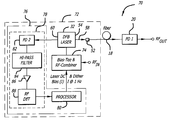
- FIG. 7 is a simplified schematic of an illustrative embodiment of a directly modulated optical link having a feedback control loop designed in accordance with the teachings of the present invention.
- FIG. 8 is a graph of experimental data for RIN int vs. the laser bias current I.
- FIG. 9 is a graph of the modeled periodic variation of the integrated RIN (RIN int ) with respect to changes in the bias current ⁇ I.
- FIG. 10 is a graph showing the measured IM 3 vs. time in a simulation using a feedback control loop designed in accordance with the teachings of the present invention.
- FIG. 1 is a simplified schematic of an externally modulated analog fiber optic link 10 of conventional design and construction.
- an input signal RF IN is modulated onto an optical carrier by an external electro-optic modulator 12 .
- a CW laser 14 generates the optical carrier signal, which is delivered to the electro-optic modulator 12 by a polarization maintaining (PM) fiber 16 .
- the modulated signal is then transmitted through optical fiber 18 until it is detected and converted to an RF signal by a photodetector 20 and amplified by a post amplifier 22 , generating an output signal RF OUT .
- PM polarization maintaining
- the input end requires a relatively expensive polarization maintaining fiber 16 .
- the external modulator 12 itself is fairly expensive, so there is a need to replace it with a less costly solution.
- One approach is to use a directly modulated diode laser as the optical source.
- FIG. 2 is a simplified schematic of a directly modulated analog fiber optic link 30 of conventional design and construction.
- the CW laser and the external modulator in the system of FIG. 1 are replaced by a single component, a directly modulated diode laser 32 .
- the RF input signal is transmitted by current modulation of the diode laser 32 to the optical fiber 18 . This is the preferred approach to replace the more expensive externally modulated link used in present systems.
- an optical isolator is typically added between the diode laser 32 and the optical fiber 18 .
- the use of an optical isolator increases the complexity of the optics needed to efficiently couple the emission of the diode laser to the optical fiber.
- optical isolators are typically specified to operate over limited temperature ranges. Their figure of merit for isolation, defined as the ratio of the reflected power to incident power at the isolator's input plane, degrades substantially outside the specified temperature range of operation.
- the present invention includes a laser transmitter having an external reflector and a novel feedback control system that simultaneously minimizes interferometric intermodulation distortion and relative intensity noise (RIN), and maintains their minimums over long periods of operation.
- RIN relative intensity noise
- FIG. 3 is an illustration showing the generation of interferometric intermodulation distortion in a directly modulated analog fiber optic link.
- Interferometric intermodulation distortion is generated when undesirable reflections cause the optical field E(t) emitted by the diode laser 32 to beat against a time-delayed version E(t ⁇ d ) of itself at the photodetector 20 (of the link's receiver).
- the photodetector 20 acts as a mixer that converts the phase-modulation ⁇ (t) in the diode's optical output to amplitude noise, with associated third order distortions (IM 3 ) for two-tone inputs.
- IM 3 third order distortions
- This wavelength chirp ( ⁇ ) and the accompanying phase modulation occur because a modulation of the gain in the diode's active medium—via current modulation—induces, at the same time, a significant fluctuation ( ⁇ n d ) in the real part (n d ) of its refractive index.
- the chirp ⁇ of the lasing wavelength ⁇ o can be significantly reduced, thereby achieving a reduction in the generation of interferometric IM 3 .
- FIG. 4 is a diagram of a prior art low chirp laser transmitter 50 having an external reflector 52 .
- the laser transmitter 50 is formed by coupling the output of a diode laser 32 (of length I d ), via its AR (anti-reflective) coated front facet 54 (with reflectivity R AR ), to an external reflector 52 .
- a fiber lens 56 couples the diode emission to a fiber pigtail 58 of refractive index n ex .
- the external reflector 52 having reflectivity R ex , is located within the fiber pigtail 58 at a distance L ex , away from the front facet 54 of the diode laser 32 . Some of the light traveling through the fiber pigtail 54 is thus reflected back towards the diode laser 32 . This forms an extended cavity between the external reflector 52 and the back facet 60 of the laser diode 32 .
- the wavelength chirp is reduced by the ratio of the diode's original optical cavity length to that of the extended-cavity laser. This reduces the generation of intermodulation distortion.
- the light (in the diode 32 ) that comes from its coupling facet 54 has an optical phase ⁇ eff that varies periodically with ⁇ ex .
- the oscillation frequency ⁇ o of the overall laser is determined from the equation:
- FIG. 5 is a graph showing RIN vs. frequency for the cases of ⁇ ex that gave rise to maximal and minimal RIN in the diode laser, compared with the diode's intrinsic RIN.
- the RIN integrated over a selected frequency bandwidth was also computed.
- the diode will demonstrate lower intensity noise than a solitary laser source (i.e. one operating without external feedback).
- a novel approach is disclosed that enables one to lock the laser to the feedback condition that supports the minimum-RIN operation condition. This serves, in turn, to enhance the SFDR of the analog photonic link.
- interferometric IM 3 was also minimized under the optimal feedback phase ⁇ ex condition for minimal RIN.
- the feedback control approach of the present invention simultaneously minimizes RIN and interferometric intermodulation distortion in a directly modulated optical link.
- the laser diode's bias current (I) is used to optimize the feedback phase ⁇ ex , thereby enabling the transmitter to operate at low RIN (and intermodulation distortion) over a long time span.
- a bias current feedback loop is used to control and lock the laser's performance parameters, so that its intensity noise and interferometric distortion are both actively minimized.
- the bias current of the diode is then adjusted so that its intensity noise always sits at a minimum.
- the third order intermodulation distortion (IM 3 ) can be reduced by 45 dB (relative to its magnitude with the loop off).
- FIG. 7 is a simplified schematic of an illustrative embodiment of a directly modulated optical link 70 having a feedback control loop designed in accordance with the teachings of the present invention.
- the signal output from a novel laser transmitter 72 is transmitted through optical fiber 18 to a first photodetector 20 , which detects and converts the signal to RF, generating an output signal RF OUT .
- the laser transmitter 72 includes a directly modulated diode laser 32 having a bias-tee and RF combiner 74 adapted to receive an input signal RF IN and a bias current I, and an external reflector 52 for forming an extended cavity to reduce chirp (as described above).
- the input signal RF IN is modulated onto an optical carrier by the diode laser 32 and output through the front facet 54 of the laser diode 32 towards the external reflector 52 .
- the external reflector 52 is integrated into the fiber pigtail 58 of the laser transmitter 72 by depositing a thin film (e.g. Si or TiO 2 ) on the cleaved surface of a short piece of fiber, which is then spliced to a longer fiber length to form a fiber pigtail 58 .
- a thin film e.g. Si or TiO 2
- Other methods for generating reflectivity may be used to form the extended cavity without departing from the scope of the present teachings.
- the laser transmitter 72 also includes a novel feedback control loop 76 adapted to control the bias current I of the diode laser 32 , such that RIN and interferometric IM 3 are minimized.
- the feedback control loop 76 includes a circuit 78 for detecting and measuring noise in the diode laser 32 , and a processor 80 adapted to receive the noise measurements from the noise measuring circuit 78 and in accordance therewith, adjust the bias current I such that RIN is minimized.
- the noise measuring circuit 78 includes a second photodetector 82 adapted to receive energy output from the back facet 60 of the diode laser source 32 (a small amount of light generated by the diode laser 32 is allowed to exit through the back facet 60 ).
- the second photodetector 82 is used to measure the level of RIN in the diode 32 .
- a high-pass RF filter 84 is used to reject the stronger photodetected signals located at the input RF frequencies.
- An RF amplifier 86 then amplifies the signal output from the high-pass filter 84 .
- the signal is fed to an RF detector 88 that effectively integrates the RIN over a selected frequency bandwidth, allowing the RIN to be more easily detected.
- the output (RIN int in Volts) of the RF detector 88 is then fed to the processor 80 .
- the processor 80 applies a low frequency (for example, about 1 Hz) current dither ( ⁇ I) to the bias current I of the laser 32 .
- the processor 80 can then estimate the derivative D from the measurements of RIN int output from the noise measuring circuit 78 (by dividing the change in measured RIN int by the change in applied bias current I).
- the processor 80 then adjusts the bias current I of the diode laser 32 so that RIN int always sits at a minimum.
- the derivative D When the RIN int is at a minimum, the derivative D will be approximately zero. If the derivative D is positive, then the bias current I should be decreased. If the derivative D is negative, then the bias current I should be increased. The laser transmitter 72 is thus locked to the minimum RIN.
- FIG. 8 is a graph of experimental data for the noise RIN int vs. the laser bias current I. As shown, the measured minimum for RIN int repeats itself, with a period of I period ⁇ 4 to 4.5 mA, with respect to the bias current of the diode.
- the bias current I of the laser is adjusted adiabatically by the feedback control loop 76 , it incurs, via thermal effects, a small change in the original (solitary) lasing frequency ⁇ o of the diode 32 .
- This thermal tuning rate is approximately ⁇ 1 ⁇ /° C. (or 17.75 GHz/° C. at ⁇ o ⁇ 1300 nm) for DFB diode lasers.
- FIG. 9 is a graph of the modeled periodic variation of the integrated RIN (RIN int ) with respect to changes in the bias current ⁇ I, using the thermal parameters mentioned above.
- This periodic variation of RIN int with I forms the basis for the bias adjustments performed by the feedback control loop 76 of the present invention.
- the graph of FIG. 8 also shows a plot of the measured IM 3 vs. bias current I when two RF tones (at frequencies f 1 and f 2 ) were used to modulate the laser diode 32 .
- the minimum of the intermodulation distortion IM 3 is co-located with the left minimum of the RIN int .
- FIG. 10 is a graph showing the measured IM 3 vs. time in a simulation using the feedback control loop 76 to lock the laser 72 to a minimum level of IM 3 , over an arbitrarily chosen operation period of ⁇ 19.1 hours. Notice that the measured IM 3 , with the loop closed, was 25-30 dB below its level measured with the loop opened.
Abstract
Description
Hence, the wavelength chirp is reduced by the ratio of the diode's original optical cavity length to that of the extended-cavity laser. This reduces the generation of intermodulation distortion.
r eff =|r eff |e jφ
where m is an integer. Thus, one can fine tune the lasing frequency Ωo—for example, to minimize RIN —by changing (i) the original (solitary) diode lasing frequency ωo (set by the second term of Eqn. 3), or (ii) the effective phase φeff of the feedback from the external reflector. (ωo is the optical oscillation frequency of the
Claims (25)
Priority Applications (1)
| Application Number | Priority Date | Filing Date | Title |
|---|---|---|---|
| US10/960,159 US7725043B2 (en) | 2004-10-07 | 2004-10-07 | System and method for reducing interferometric distortion and relative intensity noise in directly modulated fiber optic links |
Applications Claiming Priority (1)
| Application Number | Priority Date | Filing Date | Title |
|---|---|---|---|
| US10/960,159 US7725043B2 (en) | 2004-10-07 | 2004-10-07 | System and method for reducing interferometric distortion and relative intensity noise in directly modulated fiber optic links |
Publications (2)
| Publication Number | Publication Date |
|---|---|
| US20060078339A1 US20060078339A1 (en) | 2006-04-13 |
| US7725043B2 true US7725043B2 (en) | 2010-05-25 |
Family
ID=36145477
Family Applications (1)
| Application Number | Title | Priority Date | Filing Date |
|---|---|---|---|
| US10/960,159 Expired - Fee Related US7725043B2 (en) | 2004-10-07 | 2004-10-07 | System and method for reducing interferometric distortion and relative intensity noise in directly modulated fiber optic links |
Country Status (1)
| Country | Link |
|---|---|
| US (1) | US7725043B2 (en) |
Cited By (3)
| Publication number | Priority date | Publication date | Assignee | Title |
|---|---|---|---|---|
| US20090268272A1 (en) * | 2007-11-23 | 2009-10-29 | Huawei Technologies Co., Ltd. | System and method of optical modulation |
| CN103575511A (en) * | 2013-11-06 | 2014-02-12 | 湖南工学院 | Device and method for measuring relative intensity noise of laser |
| US9467227B2 (en) * | 2014-03-13 | 2016-10-11 | Luxtera, Inc. | Method and system for an optical connection service interface |
Families Citing this family (8)
| Publication number | Priority date | Publication date | Assignee | Title |
|---|---|---|---|---|
| US8165475B2 (en) * | 2007-05-24 | 2012-04-24 | Applied Optoelectronics | Systems and methods for reducing clipping in multichannel modulated optical systems |
| US8358937B2 (en) * | 2007-05-24 | 2013-01-22 | Applied Optoelectronics, Inc. | Systems and methods for reducing clipping in multichannel modulated optical systems |
| US8165474B2 (en) * | 2008-03-21 | 2012-04-24 | Applied Optoelectronics, Inc. | Reducing cross modulation in multichannel modulated optical systems with anti-clipping |
| US8891974B2 (en) | 2012-03-30 | 2014-11-18 | Applied Optoelectronics, Inc. | Distortion compensation circuit including tunable phase path |
| US9130681B2 (en) * | 2013-03-27 | 2015-09-08 | Infinera Corporation | Reducing phase noise associated with optical sources |
| JP6572659B2 (en) * | 2015-07-28 | 2019-09-11 | 富士通オプティカルコンポーネンツ株式会社 | Optical transmitter and control method |
| CN106092520B (en) * | 2016-08-02 | 2018-08-31 | 中国电子科技集团公司第三十八研究所 | The measuring device and method of Distributed Feedback Laser frequency noise |
| CN108493762B (en) * | 2018-01-26 | 2020-10-16 | 中国科学院上海光学精密机械研究所 | Semiconductor laser intensity noise suppression device and suppression method based on nonlinear effect |
Citations (18)
| Publication number | Priority date | Publication date | Assignee | Title |
|---|---|---|---|---|
| US4786132A (en) * | 1987-03-31 | 1988-11-22 | Lytel Corporation | Hybrid distributed bragg reflector laser |
| US5003546A (en) * | 1989-08-31 | 1991-03-26 | At&T Bell Laboratories | Interferometric devices for reducing harmonic distortions in laser communication systems |
| US5305336A (en) * | 1992-01-29 | 1994-04-19 | At&T Bell Laboratories | Compact optical pulse source |
| US5402433A (en) * | 1994-01-05 | 1995-03-28 | Alcatel Network Systems, Inc. | Apparatus and method for laser bias and modulation control |
| US5717708A (en) * | 1995-11-09 | 1998-02-10 | Mells; Bradley | Method and apparatus of stabilizing a semiconductor laser |
| US5761225A (en) * | 1996-05-23 | 1998-06-02 | Litton Systems, Inc. | Optical fiber amplifier eled light source with a relative intensity noise reduction system |
| US5850303A (en) * | 1996-06-14 | 1998-12-15 | Matsushita Electric Industrial Co., Ltd. | Optical transmission system and optical transmission device used therefor |
| US5870417A (en) * | 1996-12-20 | 1999-02-09 | Sdl, Inc. | Thermal compensators for waveguide DBR laser sources |
| US6068411A (en) * | 1997-06-10 | 2000-05-30 | Nec Corporation | Distortion characteristic and yield of semiconductor laser module |
| US6278721B1 (en) * | 1999-03-03 | 2001-08-21 | Lucent Technologies, Inc. | Method for minimizing locking range variability of a laser module |
| WO2002084828A2 (en) * | 2001-04-12 | 2002-10-24 | Finisar Corporation | Method and device for regulating the average wavelength of a laser, especially a semiconductor laser |
| US6580734B1 (en) * | 1999-07-07 | 2003-06-17 | Cyoptics Ltd. | Laser wavelength stabilization |
| US6839377B2 (en) * | 2001-10-26 | 2005-01-04 | Agere Systems, Inc. | Optoelectronic device having a fiber grating stabilized pump module with increased locking range and a method of manufacture therefor |
| US6862136B2 (en) * | 2002-01-31 | 2005-03-01 | Cyoptics Ltd. | Hybrid optical transmitter with electroabsorption modulator and semiconductor optical amplifier |
| US20050123008A1 (en) * | 2003-12-08 | 2005-06-09 | Daiber Andrew J. | Multiple input/output ECDL cavity length and filter temperature control |
| US20050180474A1 (en) * | 2004-02-13 | 2005-08-18 | Bianca Buchold | Low relative intensity noise fiber grating type laser diode |
| US20050220458A1 (en) * | 2004-04-02 | 2005-10-06 | K2 Optronics, A Delaware Corporation | Analog transmitter using an external cavity laser (ECL) |
| US7046704B2 (en) * | 2002-07-01 | 2006-05-16 | Mrv Communication Ltd. | Tunable laser with a fixed and stable wavelength grid especially useful for WDM in fiber optic communication systems |
-
2004
- 2004-10-07 US US10/960,159 patent/US7725043B2/en not_active Expired - Fee Related
Patent Citations (19)
| Publication number | Priority date | Publication date | Assignee | Title |
|---|---|---|---|---|
| US4786132A (en) * | 1987-03-31 | 1988-11-22 | Lytel Corporation | Hybrid distributed bragg reflector laser |
| US5003546A (en) * | 1989-08-31 | 1991-03-26 | At&T Bell Laboratories | Interferometric devices for reducing harmonic distortions in laser communication systems |
| US5305336A (en) * | 1992-01-29 | 1994-04-19 | At&T Bell Laboratories | Compact optical pulse source |
| US5402433A (en) * | 1994-01-05 | 1995-03-28 | Alcatel Network Systems, Inc. | Apparatus and method for laser bias and modulation control |
| US5717708A (en) * | 1995-11-09 | 1998-02-10 | Mells; Bradley | Method and apparatus of stabilizing a semiconductor laser |
| US5761225A (en) * | 1996-05-23 | 1998-06-02 | Litton Systems, Inc. | Optical fiber amplifier eled light source with a relative intensity noise reduction system |
| US5850303A (en) * | 1996-06-14 | 1998-12-15 | Matsushita Electric Industrial Co., Ltd. | Optical transmission system and optical transmission device used therefor |
| US5870417A (en) * | 1996-12-20 | 1999-02-09 | Sdl, Inc. | Thermal compensators for waveguide DBR laser sources |
| US6068411A (en) * | 1997-06-10 | 2000-05-30 | Nec Corporation | Distortion characteristic and yield of semiconductor laser module |
| US6278721B1 (en) * | 1999-03-03 | 2001-08-21 | Lucent Technologies, Inc. | Method for minimizing locking range variability of a laser module |
| US6580734B1 (en) * | 1999-07-07 | 2003-06-17 | Cyoptics Ltd. | Laser wavelength stabilization |
| WO2002084828A2 (en) * | 2001-04-12 | 2002-10-24 | Finisar Corporation | Method and device for regulating the average wavelength of a laser, especially a semiconductor laser |
| US20040190570A1 (en) * | 2001-04-12 | 2004-09-30 | Bernd Hubner | Method and device for regulating the average wavelength of a laser, especially a semiconductor laser |
| US6839377B2 (en) * | 2001-10-26 | 2005-01-04 | Agere Systems, Inc. | Optoelectronic device having a fiber grating stabilized pump module with increased locking range and a method of manufacture therefor |
| US6862136B2 (en) * | 2002-01-31 | 2005-03-01 | Cyoptics Ltd. | Hybrid optical transmitter with electroabsorption modulator and semiconductor optical amplifier |
| US7046704B2 (en) * | 2002-07-01 | 2006-05-16 | Mrv Communication Ltd. | Tunable laser with a fixed and stable wavelength grid especially useful for WDM in fiber optic communication systems |
| US20050123008A1 (en) * | 2003-12-08 | 2005-06-09 | Daiber Andrew J. | Multiple input/output ECDL cavity length and filter temperature control |
| US20050180474A1 (en) * | 2004-02-13 | 2005-08-18 | Bianca Buchold | Low relative intensity noise fiber grating type laser diode |
| US20050220458A1 (en) * | 2004-04-02 | 2005-10-06 | K2 Optronics, A Delaware Corporation | Analog transmitter using an external cavity laser (ECL) |
Non-Patent Citations (9)
| Title |
|---|
| Ball et al: "60 mW 1.5 mm Single-Frequency Low-Noise Fiber Laser MOPA", IEEE Photonics Technology Letters, vol. 6, No. 2, Feb. 1994, p. 192-194. * |
| Ball et al: "60 mW 1.5 um Single-Frequency Low-Noise Fiber Laser MOPA", IEEE Photonics Technology Letters, vol. 6, No. 2, Feb. 1994, p. 192-194). * |
| D.J. Ottaway, P.J. Veitch, C. Hollitt, D. Mudge, M.W. Hamilton and J. Munch, "Frequency and intensity noise of an injection-locked Nd:YAG ring laser," Appl. Phys. B 71, 2000, pp. 163-168. |
| F. Rogister, D. Sukow, A. Gavrielides, P. Megret, O. Deparis and M. Blondel, "Experimental demonstration of suppression of low-frequency fluctuations and stabilization of an external-cavity laser diode," Optics Letters, vol. 25, No. 11, Jun. 1, 2000, pp. 808-810. |
| G.P. Agrawal and N.K. Dutta, "Long-Wavelength Semiconductor Lasers," Van Nostrand Reinhold, 1986, p. 316. |
| G.P.Agrawal, N.A. Olsson and N.K. Dutta, "Effect of fiber-far-end reflections on intensity and phase noise in InGaAsP semiconductor lasers," Applied Phys. Lett. 45(6), 1984, p. 597-599. |
| J. Zhang, C. Xie and K. Peng, "Electronic feedback control of the intensity noise of a single-frequency intracavity-doubled laser," J. Opt. Soc. Am. B/vol. 19, No. 8, August 2002. |
| J. Zhang, H. Chang, X. Jia, H. Lei, R. Want, C. Xie and K. Peng, "Suppression of the intensity noise of a laser-diode-pumped single-frequency ring Nd:YVO4-KTP green laser by optoelectronic feedback," Optics Letters, vol. 26, No. 10, May 15, 2001, pp. 695-697. |
| M.Osinski and J. Buus, "Linewidth Broadening Factor in Semiconductor Lasers-An Overview," IEEE Journal of Quantum Electronics, vol. QE-23, No. 1, Jan. 1987, pp. 9-29. |
Cited By (8)
| Publication number | Priority date | Publication date | Assignee | Title |
|---|---|---|---|---|
| US20090268272A1 (en) * | 2007-11-23 | 2009-10-29 | Huawei Technologies Co., Ltd. | System and method of optical modulation |
| CN103575511A (en) * | 2013-11-06 | 2014-02-12 | 湖南工学院 | Device and method for measuring relative intensity noise of laser |
| US9467227B2 (en) * | 2014-03-13 | 2016-10-11 | Luxtera, Inc. | Method and system for an optical connection service interface |
| US20170026124A1 (en) * | 2014-03-13 | 2017-01-26 | Luxtera, Inc. | Method And System For An Optical Connection Service Interface |
| US9929811B2 (en) * | 2014-03-13 | 2018-03-27 | Luxtera, Inc. | Method and system for an optical connection service interface |
| US10439725B2 (en) * | 2014-03-13 | 2019-10-08 | Luxtera, Inc. | Method and system for an optical connection service interface |
| US20200052791A1 (en) * | 2014-03-13 | 2020-02-13 | Luxtera, Inc. | Method And System For An Optical Connection Service Interface |
| US10848246B2 (en) * | 2014-03-13 | 2020-11-24 | Luxtera Llc | Method and system for an optical connection service interface |
Also Published As
| Publication number | Publication date |
|---|---|
| US20060078339A1 (en) | 2006-04-13 |
Similar Documents
| Publication | Publication Date | Title |
|---|---|---|
| Pillet et al. | Dual-frequency laser at 1.5 µm for optical distribution and generation of high-purity microwave signals | |
| Peterman et al. | Noise and distortion characteristics of semiconductor lasers in optical fiber communication systems | |
| AU2007302314B2 (en) | Method and device for generating a synthetic wavelength | |
| US7471710B2 (en) | Narrow linewidth semiconductor laser device | |
| US20130215919A1 (en) | Wideband tunable laser line-width reduction | |
| US8472022B2 (en) | Spectroscopic detection system and method | |
| Kourogi et al. | Limit of optical-frequency comb generation due to material dispersion | |
| US8717657B2 (en) | Optoelectronic oscillator using a high finesse etalon | |
| CN110176709A (en) | Integrated Fourier mode locking optical-electronic oscillator and application and communication system | |
| WO2001052371A1 (en) | Optical pulse synthesis using brillouin selective sideband amplification | |
| US7725043B2 (en) | System and method for reducing interferometric distortion and relative intensity noise in directly modulated fiber optic links | |
| Aflatouni et al. | Design methodology and architectures to reduce the semiconductor laser phase noise using electrical feedforward schemes | |
| Nagarajan et al. | Millimeter wave narrowband optical fiber links using external cavity semiconductor lasers | |
| Conforti et al. | Acoustical and 1∕ f noises in narrow linewidth lasers | |
| Liu et al. | Hybrid integrated frequency-modulated continuous-wave laser with synchronous tuning | |
| WO2016161638A1 (en) | Coherent receiver for frequency offset estimation and compensation of coherent light source, method and system | |
| US7620081B2 (en) | Semiconductor laser utilizing real-time linewidth reduction method | |
| Bowers | Integrated microwave photonics | |
| Nelson et al. | Relative intensity noise suppression for RF photonic links | |
| JP6941121B2 (en) | Spectral narrowing module, narrowing spectral line device, and methods for doing so | |
| Li et al. | Tunable Microwave Frequency Comb Generation Based on Actively Mode-Locked OEO | |
| US11539185B2 (en) | Laser apparatus | |
| Nakagawa et al. | Modulation-free acetylene-stabilized lasers at 1542 nm using modulation transfer spectroscopy | |
| JP3351212B2 (en) | Pulse light source | |
| Pajarola et al. | Frequency tunable beat note from a dual-polarization emitting external cavity diode laser |
Legal Events
| Date | Code | Title | Description |
|---|---|---|---|
| AS | Assignment |
Owner name: RAYTHEON COMPANY, MASSACHUSETTS Free format text: ASSIGNMENT OF ASSIGNORS INTEREST;ASSIGNORS:NG, WILLIE W.;PERSECHINI, DAVID L.;BUCKLEY, ROBERT H.;REEL/FRAME:015881/0762;SIGNING DATES FROM 20040827 TO 20041004 Owner name: RAYTHEON COMPANY,MASSACHUSETTS Free format text: ASSIGNMENT OF ASSIGNORS INTEREST;ASSIGNORS:NG, WILLIE W.;PERSECHINI, DAVID L.;BUCKLEY, ROBERT H.;SIGNING DATES FROM 20040827 TO 20041004;REEL/FRAME:015881/0762 |
|
| STCF | Information on status: patent grant |
Free format text: PATENTED CASE |
|
| FPAY | Fee payment |
Year of fee payment: 4 |
|
| MAFP | Maintenance fee payment |
Free format text: PAYMENT OF MAINTENANCE FEE, 8TH YEAR, LARGE ENTITY (ORIGINAL EVENT CODE: M1552) Year of fee payment: 8 |
|
| FEPP | Fee payment procedure |
Free format text: MAINTENANCE FEE REMINDER MAILED (ORIGINAL EVENT CODE: REM.); ENTITY STATUS OF PATENT OWNER: LARGE ENTITY |
|
| LAPS | Lapse for failure to pay maintenance fees |
Free format text: PATENT EXPIRED FOR FAILURE TO PAY MAINTENANCE FEES (ORIGINAL EVENT CODE: EXP.); ENTITY STATUS OF PATENT OWNER: LARGE ENTITY |
|
| STCH | Information on status: patent discontinuation |
Free format text: PATENT EXPIRED DUE TO NONPAYMENT OF MAINTENANCE FEES UNDER 37 CFR 1.362 |
|
| FP | Lapsed due to failure to pay maintenance fee |
Effective date: 20220525 |