US7719921B2 - Duty detection circuit, DLL circuit using the same, semiconductor memory circuit, and data processing system - Google Patents
Duty detection circuit, DLL circuit using the same, semiconductor memory circuit, and data processing system Download PDFInfo
- Publication number
- US7719921B2 US7719921B2 US12/170,730 US17073008A US7719921B2 US 7719921 B2 US7719921 B2 US 7719921B2 US 17073008 A US17073008 A US 17073008A US 7719921 B2 US7719921 B2 US 7719921B2
- Authority
- US
- United States
- Prior art keywords
- circuit
- clock signal
- internal clock
- control signals
- signal
- Prior art date
- Legal status (The legal status is an assumption and is not a legal conclusion. Google has not performed a legal analysis and makes no representation as to the accuracy of the status listed.)
- Active, expires
Links
Images


Classifications
-
- G—PHYSICS
- G11—INFORMATION STORAGE
- G11C—STATIC STORES
- G11C11/00—Digital stores characterised by the use of particular electric or magnetic storage elements; Storage elements therefor
- G11C11/21—Digital stores characterised by the use of particular electric or magnetic storage elements; Storage elements therefor using electric elements
- G11C11/34—Digital stores characterised by the use of particular electric or magnetic storage elements; Storage elements therefor using electric elements using semiconductor devices
- G11C11/40—Digital stores characterised by the use of particular electric or magnetic storage elements; Storage elements therefor using electric elements using semiconductor devices using transistors
- G11C11/401—Digital stores characterised by the use of particular electric or magnetic storage elements; Storage elements therefor using electric elements using semiconductor devices using transistors forming cells needing refreshing or charge regeneration, i.e. dynamic cells
- G11C11/4063—Auxiliary circuits, e.g. for addressing, decoding, driving, writing, sensing or timing
- G11C11/407—Auxiliary circuits, e.g. for addressing, decoding, driving, writing, sensing or timing for memory cells of the field-effect type
- G11C11/4076—Timing circuits
-
- G—PHYSICS
- G11—INFORMATION STORAGE
- G11C—STATIC STORES
- G11C7/00—Arrangements for writing information into, or reading information out from, a digital store
- G11C7/22—Read-write [R-W] timing or clocking circuits; Read-write [R-W] control signal generators or management
-
- G—PHYSICS
- G11—INFORMATION STORAGE
- G11C—STATIC STORES
- G11C7/00—Arrangements for writing information into, or reading information out from, a digital store
- G11C7/22—Read-write [R-W] timing or clocking circuits; Read-write [R-W] control signal generators or management
- G11C7/222—Clock generating, synchronizing or distributing circuits within memory device
-
- H—ELECTRICITY
- H03—ELECTRONIC CIRCUITRY
- H03L—AUTOMATIC CONTROL, STARTING, SYNCHRONISATION, OR STABILISATION OF GENERATORS OF ELECTRONIC OSCILLATIONS OR PULSES
- H03L7/00—Automatic control of frequency or phase; Synchronisation
- H03L7/06—Automatic control of frequency or phase; Synchronisation using a reference signal applied to a frequency- or phase-locked loop
- H03L7/08—Details of the phase-locked loop
- H03L7/081—Details of the phase-locked loop provided with an additional controlled phase shifter
- H03L7/0812—Details of the phase-locked loop provided with an additional controlled phase shifter and where no voltage or current controlled oscillator is used
- H03L7/0814—Details of the phase-locked loop provided with an additional controlled phase shifter and where no voltage or current controlled oscillator is used the phase shifting device being digitally controlled
-
- H—ELECTRICITY
- H03—ELECTRONIC CIRCUITRY
- H03L—AUTOMATIC CONTROL, STARTING, SYNCHRONISATION, OR STABILISATION OF GENERATORS OF ELECTRONIC OSCILLATIONS OR PULSES
- H03L7/00—Automatic control of frequency or phase; Synchronisation
- H03L7/06—Automatic control of frequency or phase; Synchronisation using a reference signal applied to a frequency- or phase-locked loop
- H03L7/08—Details of the phase-locked loop
- H03L7/085—Details of the phase-locked loop concerning mainly the frequency- or phase-detection arrangement including the filtering or amplification of its output signal
- H03L7/087—Details of the phase-locked loop concerning mainly the frequency- or phase-detection arrangement including the filtering or amplification of its output signal using at least two phase detectors or a frequency and phase detector in the loop
Definitions
- the present invention relates to a duty detection circuit and a DLL circuit using the same, and, more particularly relates to a duty detection circuit suitable for detecting a duty of an internal clock signal used in a DDR (Double Data Rate) synchronous DRAM, and a DLL circuit using the circuit.
- the present invention also relates to a semiconductor memory device using the DLL circuit, and a data processing system using the semiconductor memory device.
- a DLL Delay Locked Loop
- the DLL circuit is provided with a duty detection circuit so that a duty of the internal clock signal becomes 50% (see Japanese Patent Application Laid-open No. 2006-303553).
- FIG. 9 is a circuit diagram of a conventional duty detection circuit.
- the duty detection circuit shown in FIG. 9 includes a detection line LDUTYHB connected to a contact node between a discharge transistor TR 1 and a charge transistor TR 3 , a detection line LDUTYLB connected to a contact node between a discharge transistor TR 2 and a charge transistor TR 4 , and a comparator circuit COMP that detects a potential difference of these detection lines LDUTYHB and LDUTYLB.
- Capacitances C 1 and C 2 are connected to the detection line LDUTYHB, and capacitances C 3 and C 4 are connected to the detection line LDUTYLB.
- the discharge transistor TR 1 and the charge transistor TR 3 are controlled by gate circuits G 1 and G 3 , respectively, and are brought into on state in response to an internal clock signal LCLKOET and a selection signal LDCSMT, respectively.
- the discharge transistor TR 2 and the charge transistor TR 4 are controlled by gate circuits G 2 and G 4 , respectively, and are brought into on state in response to an internal clock signal LCLKOEB and a selection signal LDCSMB, respectively.
- the internal clock signal LCLKOET and the internal clock signal LCLKOEB are internal clock signals for duty detection, and are mutually complementary signals.
- Sources of the discharge transistors TR 1 and TR 2 are connected in common to a discharge node BIASND.
- the discharge node BIASND is connected to a ground potential via a bias transistor N 1 .
- a precharge circuit P 0 operating based on a precharge signal PRE is connected to the charge transistors TR 3 and TR 4 .
- FIG. 10 is an operation waveform diagram of the duty detection circuit shown in FIG. 9 .
- the selection signal LDCSMT is activated during a period of a clock edge 0 to a clock edge 4
- the selection signal LDCSMB is activated during a period of a clock edge 1 to a clock edge 5 . That is, these selection signals are activated with a half cycle deviation of the internal clock signal.
- the detection line LDUTYHB is discharged when the internal clock signal LCLKOET becomes at a high level and is charged when the internal clock signal LCLKOET becomes at a low level, during a period while the selection signal LDCSMT is activated.
- the detection line LDUTYLB is discharged when the internal clock signal LCLKOEB becomes at a high level and is charged when the internal clock signal LCLKOEB becomes at a low level, during a period while the selection signal LDCSMB is activated.
- the comparator circuit COMP detects a potential difference ⁇ V obtained in this way, and generates a duty detection signal LUPDCT.
- the conventional duty detection circuit shown in FIG. 9 has a problem in that discharge speeds of the discharge transistors TR 1 and TR 2 are different at the detection starting time. That is, while the discharge transistor TR 1 is turned on at the clock edge 0 , both the discharge transistors TR 1 and TR 2 are off during a preceding period. Therefore, a discharge node BIASND at the detection starting time is substantially at a ground potential. On the other hand, because the discharge transistor TR 2 is turned on at the clock edge 1 , the discharge node BIASND already increases at the detection starting time. Consequently, a difference occurs between the discharge speeds of the discharge transistors TR 1 and TR 2 , and an accurate detection of duty cannot be performed.
- the conventional duty detection circuit shown in FIG. 9 has continuous two cycles as a detection period. Therefore, only an average value of the duty in an even cycle and the duty in an odd cycle can be obtained. For example, when the duty in the even cycle is 60% and when the duty of the odd cycle is 40%, the average value becomes 50%. As a result, duty correction is not performed.
- the two-phase DLL is a system that generates two frequency-divided signals by dividing an external clock signal into two, and generates an internal clock signal by combining the two frequency-divided signals after adjusting a delay amount of the frequency-divided signals. This type of DLL circuit is often used when the frequency of the external clock signal is high.
- the duty in the even cycle does not coincide with the duty in the odd cycle is some cases. In this case, the duty detection circuit shown in FIG. 9 cannot perform accurate detection.
- FIG. 11 is a circuit diagram of the improved duty detection circuit.
- the duty detection circuit shown in FIG. 11 additionally includes a delay circuit D 1 that delays the output of the gate circuit G 2 while deleting the charge transistors TR 3 and TR 4 and the gate circuits G 3 and G 4 that control these charge transistors, in the duty detection circuit shown in FIG. 9 .
- FIG. 12 is an operation waveform diagram of the duty detection circuit shown in FIG. 11 .
- the selection signal LDCSMT is activated by dividing the period into a period of the clock edges 0 to 2 and a period of the clock edges 4 to 6
- the selection signal LDCSMB is activated by dividing the period into a period of the clock edges 1 to 3 and a period of the clock edges 5 to 7 .
- the selection signal as an output of the gate circuits G 1 and G 2 has a waveform corresponding to only the even cycle of the internal clock signal.
- the duty detection circuit shown in FIG. 11 can detect a duty by extracting only the duty in the even cycle (or the odd cycle). Consequently, by providing the duty detection circuit for the even cycle and the duty detection circuit for the odd cycle, these duty detection circuits can be applied to the two-phase DLL circuit.
- the output of the gate circuit G 2 can be supplied to the discharge transistor TR 2 after being delayed by the delay circuit D 1 , a period during which both transistors are turned off are inserted into between the on period of the discharge transistor TR 1 and the on period of the discharge transistor TR 2 . Consequently, when the discharge transistors TR 1 and TR 2 change from off to on, the potential of the discharge node BIASND is precharged to about a ground potential, and there arises no difference in discharge speeds.
- the potential difference ⁇ V appearing in the detection lines LDUTYHB and LDUTYLB is smaller than that in the duty detection circuit shown in FIG. 9 .
- This problem is considered to be solved by adding the charge transistors TR 3 and TR 4 to the duty detection circuit shown in FIG. 11 .
- other problems occur such as a variation between the control at the charge side and the control at the discharge side, and a variation between the control at the detection line LDUTYHB side and the control at the detection line LDUTYLB side.
- Another object of the present invention is to provide a semiconductor memory device using the DLL circuit.
- Still another object of the present invention is to provide a data processing system using the semiconductor memory device.
- a duty detection circuit comprises:
- first and second discharge transistors that operate in response to first and second control signals
- first and second charge transistors that operate in response to third and fourth control signals
- a first detection line connected to a contact node between the first discharge transistor and the first charge transistor
- a second detection line connected to a contact node between the second discharge transistor and the second charge transistor
- a comparator circuit that detects a potential difference between the first and second detection lines
- a first gate circuit that can activate the first control signal when an internal clock signal being at a high level during every n cycles (where n is a power of 2) of an internal clock signal;
- a second gate circuit that can activate the second control signal when the internal clock signal being at a low level during every n cycles of the internal clock signal
- a third gate circuit that can activate the third control signal when the internal clock signal being at the low level during every n cycles of the internal clock signal
- a fourth gate circuit that can activate the fourth control signal when the internal clock signal being at the high level during every n cycles of the internal clock signal
- a second delay circuit that delays one of the third and fourth control signals.
- a DLL circuit according to the present invention comprises:
- n is a power of 2
- n is a power of 2
- n delay adjusting units that adjust the phases of the frequency-divided signals
- a combining circuit that generates an internal clock signal by combining outputs from the n delay adjusting units
- the duty detection circuit having above described configuration that detects a duty of the internal clock signal, and an output signal of the duty detection circuit is fed back to at least one of the n delay adjusting units.
- a semiconductor memory device includes said DLL circuit.
- a data processing system includes said semiconductor memory device.
- the first and second detection lines are charged and discharged corresponding to the internal clock signal of an n-time cycle. Therefore, the duty detection circuit can be applied to the multi-phase DLL circuit, and a potential difference appearing in the detection line can be sufficiently secured. Further, a delay circuit is provided at not only the discharge side but also the charge side. Therefore, the discharge speed and the charge speed can be also secured at a constant level.
- the first gate circuit receives the internal clock signal and a first selection signal, and generates the first control signal
- the second gate circuit receives an inverted signal of the internal clock signal and a second selection signal, and generates the second control signal
- the third gate circuit receives the inverted signal and a third selection signal, and generates the third control signal
- the fourth gate circuit receives the internal clock signal and a fourth selection signal, and generates the fourth control signal. According to this configuration, the number of stages of each gate circuit can be minimized.
- the numbers of the first to fourth control signals that active corresponding each detection period are mutually equal. According to this configuration, the detection variation can be minimized.
- a duty detection circuit that can be applied to the multi-phase DLL circuit, can hold the discharge speed and the charge speed at a constant level, and can have a large potential difference appearing in the detection line. Further, it is possible to provide a DLL circuit and a semiconductor memory device using the duty detection circuit.
- FIG. 1 is a circuit diagram of a duty detection circuit according to a preferred embodiment of the present invention
- FIG. 2 is an operation waveform diagram of the duty detection circuit shown in FIG. 1 ;
- FIG. 3 is a schematic timing diagram for explaining the charge and discharge operations performed during detection periods
- FIG. 4 is a block diagram of a DLL circuit using the duty detection circuit shown in FIG. 1 ;
- FIG. 5 is a block diagram showing a configuration of a data processing system using a semiconductor memory device according to a preferred embodiment of the present invention
- FIG. 6 is a circuit diagram of a duty detection circuit according to a modified embodiment of the present invention.
- FIG. 7 is a circuit diagram of a duty detection circuit according to another modified embodiment of the present invention.
- FIG. 8 is a circuit diagram of a duty detection circuit according to still another modified embodiment of the present invention.
- FIG. 9 is a circuit diagram of a conventional duty detection circuit
- FIG. 10 is an operation waveform diagram of the duty detection circuit shown in FIG. 9 ;
- FIG. 11 is a circuit diagram of the improved duty detection circuit.
- FIG. 12 is an operation waveform diagram of the duty detection circuit shown in FIG. 11 .
- FIG. 1 is a circuit diagram of a duty detection circuit according to a preferred embodiment of the present invention.
- the duty detection circuit includes the discharge transistors TR 1 and TR 2 that are turned on in response to control signals A and B, respectively, the charge transistors TR 3 and TR 4 that are turned on in response to control signals D and C, respectively, the detection line LDUTYHB connected to a contact node between the discharge transistor TR 1 and the charge transistor TR 3 , the detection line LDUTYLB connected to a contact node between the discharge transistor TR 2 and the charge transistor TR 4 , and the comparator circuit COMP that detects a potential difference of these detection lines LDUTYHB and LDUTYLB.
- the capacitances C 1 and C 2 are connected to the detection line LDUTYHB, and the capacitances C 3 and C 4 are connected to the detection line LDUTYLB.
- the transistors TR 1 to TR 4 are controlled by gate circuits G 11 to G 14 , respectively.
- the gate circuit G 11 is an AND gate that receives the internal clock signal LCLKOET and a selection signal LDCSMTT. When these signals are brought into a high level, a control signal A is activated.
- the gate circuit G 12 is an AND gate that receives the internal clock signal LCLKOEB and a selection signal LDCSMBT. When these signals are brought into a high level, a control signal B 0 is activated.
- the gate circuit G 13 is a NAND gate that receives the internal clock signal LCLKOEB and a selection signal LDCSMBB. When these signals are brought into a high level, a control signal D 0 is activated.
- the gate circuit G 14 is a NAND gate that receives the internal clock signal LCLKOET and a selection signal LDCSMTB. When these signals are brought into a high level, a control signal C is activated.
- an AND gate includes a combination of a NAND gate and an inverter. Therefore, the discharge transistors TR 1 and TR 2 are controlled respectively by a signal passing through a two-stage logic circuit. On the other hand, the charge transistors TR 3 and TR 4 are controlled respectively by a signal passing through a one-stage logic circuit. As explained above, according to the circuit configuration of the present embodiment, the number of stages of each gate circuit can be minimized, signal paths controlling the discharge transistors TR 1 and TR 2 are balanced, and signal paths controlling the discharge transistors TR 3 and TR 4 are balanced. Therefore, a satisfactory circuit characteristic can be obtained.
- control signals A and C are supplied directly to the gate circuits G 11 and G 14 .
- control signals B 0 and D 0 are supplied to the gate circuits G 12 and G 13 after being passed through delay circuits D 11 and D 12 , respectively.
- the signals passing through the delay circuits D 11 and D 12 are denoted as control signals B and D. Delay amounts of the delay circuits D 11 and D 12 are set to at least a half cycle of the internal clock signal.
- Sources of the discharge transistors TR 1 and TR 2 are connected in common to the discharge node BIASND.
- the discharge node BIASND is connected to the ground potential via the bias transistor N 1 .
- sources of the charge transistors TR 3 and TR 4 are connected in common to the charge node BIASPD.
- the charge node BIASPD is connected to the power source potential via the bias transistor P 1 .
- the precharge signal PRE is supplied to the gate of the bias transistor P 1
- an inverted signal of the precharge signal PRE is supplied to the gate of the bias transistor N 1 .
- the precharge circuit P 0 is connected to the detection lines LDUTYHB and LDUTYLB.
- the precharge circuit P 0 precharges the detection lines LDUTYHB and LDUTYLB to an intermediate potential VPERDH, and is activated in response to the precharge signal PRE.
- the intermediate potential VPERDH is a potential between the ground potential and the power source potential, and is preferably a half potential of the power source potential.
- the duty detection circuit according to the present embodiment includes not only the discharge transistors but also the charge transistors. Therefore, as compared with the conventional duty detection circuit shown in FIG. 11 , a potential difference generated in the detection lines LDUTYHB and LDUTYLB can be enlarged.
- FIG. 2 is an operation waveform diagram of the duty detection circuit shown in FIG. 1 .
- the selection signal LDCSMTT is activated at three times during a period of the clock edges 0 to 2 , a period of the clock edges 4 to 6 , and a period of the clock edges 12 to 14 .
- the selection signal LDCSMBT is activated at three times during a period of the clock edges 1 to 3 , a period of the clock edges 5 to 7 , and a period of the clock edges 9 to 11 .
- the selection signal LDCSMBB is activated at three times during a period of the clock edges 1 to 3 , a period of the clock edges 9 to 11 , and a period of the clock edges 13 to 15 .
- the control signals A to D as the outputs of the gate circuits G 11 to G 14 have waveforms corresponding to only the even cycles of the internal clock signal.
- the duty detection circuit according to the present embodiment can extract and detect only a duty in the even cycle (or the odd cycle). Consequently, the duty detection circuit can be applied to the two-phase DLL circuit by providing a duty detection circuit for the even cycle and a duty detection circuit for the odd cycle.
- the output of the gate circuit G 12 is supplied to the discharge transistor TR 2 after being delayed by the delay circuit D 11 . Therefore, a period during which both the discharge transistor TR 1 and the discharge transistor TR 2 are turned off is inserted into between the on period of the discharge transistor TR 1 and the on period of the discharge transistor TR 2 , by only the amount delayed by the delay circuit D 11 . Consequently, when the discharge transistors TR 1 and TR 2 change from off to on, the potential of the discharge node BIASND is substantially precharged to the ground potential, and no difference occurs in the discharge speed.
- the output of the gate circuit G 13 is supplied to the charge transistor TR 3 after being delayed by the delay circuit D 12 . Therefore, a period during which both the charge transistor TR 3 and the charge transistor TR 4 are turned off is inserted into between the on period of the charge transistor TR 3 and the on period of the charge transistor TR 4 , by only the amount delayed by the delay circuit D 12 . Consequently, when the charge transistors TR 3 and TR 4 change from off to on, the potential of the charge node BIASPD is substantially precharged to the power source potential, and no difference occurs in the charge speed.
- FIG. 3 is a schematic timing diagram for explaining the charge and discharge operations performed during detection periods.
- the period of the clock edges 0 to 2 corresponds to a first detection period, and the control signals A, B, and D are activated corresponding to this period.
- charge and discharge of the detection line LDUTYHB and discharge of the detection line LDUTYLB are performed.
- the period of the clock edges 4 to 6 corresponds to a second detection period, and the control signals A, B, and C are activated corresponding to this period. As a result, discharge of the detection line LDUTYHB and charge and discharge of the detection line LDUTYLB are performed.
- the period of the clock edges 8 to 10 corresponds to a third detection period, and the control signals B, C, and D are activated corresponding to this period. As a result, charge of the detection line LDUTYHB and charge and discharge of the detection line LDUTYLB are performed.
- the period of the clock edges 12 to 14 corresponds to a fourth detection period, and the control signals A, C, and D are activated corresponding to this period. As a result, charge and discharge of the detection line LDUTYHB and charge of the detection line LDUTYLB are performed.
- detection variation can be minimized. That is, when there is a variation in the number of control signals to be activated corresponding to each detection cycle, a difference occurs between the charge and discharge conditions of the detection line LDUTYHB and the charge and discharge conditions of the detection line LDUTYLB. However, when the number of control signals to be activated corresponding to each detection cycle is constant, the difference of conditions can be substantially avoided. Further, the time necessary for the detection can be shortened from the time when the number of control signals to be activated corresponding to each detection cycle is one or two.
- the charge and discharge pattern according to the present embodiment has no unbalance between the control at the charge side and the control at the discharge side, and has no unbalance between the control at the detection line LDUTYHB side and the control at the detection line LDUTYLB side. Therefore, duty detection can be performed in very high precision.
- FIG. 4 is a block diagram of a DLL circuit using the duty detection circuit according to the present embodiment.
- the DLL circuit shown in FIG. 4 is a circuit used in a DDR synchronous DRAM as a semiconductor memory device, for example.
- An input external clock signal CLK is input to the DLL circuit via an input receiver 31 exclusive for the DLL circuit.
- a clock input from the input receiver 31 is frequency-divided synchronously with a rising edge by a frequency-dividing circuit 32 .
- a frequency-divided clock signal L 1 CLDINB is generated.
- a clock input from an input receiver 43 exclusive for the DLL circuit is divided synchronously with a falling edge (a rising edge of an inverted clock signal CLKB) by a frequency-dividing circuit 44 .
- a frequency-divided clock signal L 2 CLDINB is generated.
- the frequency-divided internal clock signals L 1 CLDINB and L 2 CLDINB are input to their respective delay adjusting units (delay lines) 33 and 45 .
- the delay line 33 receives the frequency-divided internal clock signal L 1 CLDINB, delays this by a predetermined amount, and generates internal clock signals L 1 CLKOET/B.
- the internal clock signals L 1 CLKOET/B are input to DQ replica circuits 34 and 38 that perform the same operations as those of the DQ buffer that outputs data.
- the outputs of the DQ replica circuits 34 and 38 are supplied to phase detection circuits 35 and 39 , and their phases are compared with a phase of the external clock signal CLK. A result of the phase comparison is fed back to the delay line 33 , and a delay amount of the delay line 33 is adjusted so that the outputs of the DQ replica circuits 34 and 38 are synchronous with the rise of the external clock signal CLK.
- the phase detection circuit 35 detects a phase of the rising edge of the external clock signal CLK in the even cycle, and inputs a detected result to a Rise_Even counter 37 via a Rise_Even controller 36 . In response to this, the Rise_Even counter 37 adjusts a phase of the rising edge of the frequency-divided clock signal L 1 CLDINB.
- the phase detection circuit 39 detects a phase of the rising edge of the external clock signal CLK in the odd cycle, and inputs a detected result to a Rise_Odd counter 41 via a Rise_Odd controller 40 . In response to this, the Rise_Odd counter 41 adjusts a phase of the rising edge of the frequency-divided clock signal L 1 CLDINB. As explained above, in the delay line 33 , both phases of the rising edge and the falling edge of the frequency-divided clock signal are adjusted.
- the delay amount of the delay line 45 to which the frequency-divided clock signal L 2 CLDINB is input is adjusted so that the duty of the output data from the DQ buffer becomes 50%.
- the delay line 45 receives the frequency-divided internal clock signal L 2 CLDINB, delays this by a predetermined amount, and generates internal clock signals L 2 CLKOET/B.
- L 1 CLKOET/B as the output of the delay line 33 and L 2 CLKOET/B as the output of the delay line 4 are combined by the multiplexer 42 , and the internal clock signals LCLKOET/B are generated.
- the internal clock signals LCLKOET/B are supplied to duty detection circuits 46 and 47 . Based on a result of the determination, a delay amount of the delay line 45 is adjusted.
- the rising edges of the generated internal clock signals LCLKOET/B are adjusted by the delay line 33 , and the falling edges are adjusted by the delay line 45 .
- Clock signals LCKOET/B after the adjustment are supplied to the DQ buffer unit. As a result, the timings of the data output by the DQ buffer are synchronized with the external clock signal CLK.
- the duty detection circuit 46 is that for the even cycle, and the duty detection circuit 47 is that for the odd cycle.
- the duty detection circuit 46 for the even cycle receives the internal clock signals LCLKOET/B, and the selection signals LDCSMTT to LDCSMBB from a DCC controller 48 , and detects the duty of the internal clock signal in the even cycle, based on this. Detailed operations are as explained above.
- the determination signal L 2 DCT_Even as the output of the DCC controller 48 is supplied to a Fall_Even counter 51 via the Fall_Even controller 50 .
- the Fall_Even counter 51 adjusts the phase of the rising edge of the frequency-divided clock signal L 2 CLDINB. As a result, the duties of the internal clock signals LCLKOET/B in the even cycle are corrected to 50%.
- the duty detection circuit 47 for the odd cycle receives the internal clock signals LCLKOET/B and the selection signals LDCSMTT to LDCSMBB from a DCC controller 49 , and detects the duty of the internal clock signal in the odd cycle based on this.
- the determination signal L 2 DCT_Odd as the output of the DCC controller 49 is supplied to a Fall_Odd counter 53 via a Fall_Odd controller 52 .
- the Fall_Odd counter 53 adjusts the phase of the falling edge of the frequency-divided clock signal L 2 CLDINB.
- the duties of the internal clock signals LCLKOET/B in the odd cycle are also corrected to 50%.
- the configuration of the DLL circuit according to the present embodiment is as described above.
- the duty in the even cycle and the duty in the odd cycle can be adjusted to 50%, respectively.
- the above DLL circuit can be used for the DDR synchronous DRAM as described above.
- FIG. 5 is a block diagram showing a configuration of a data processing system 100 using a semiconductor memory device according to a preferred embodiment of the present invention.
- the semiconductor memory device according to the present embodiment is a DRAM.
- the data processing system 100 shown in FIG. 5 includes a data processor 120 and a semiconductor memory device (DRAM) 130 according to the present embodiment connected to each other via a system bus 110 .
- the data processor 120 includes a microprocessor (MPU) and a digital signal processor (DSP), for example.
- MPU microprocessor
- DSP digital signal processor
- the constituent elements of the data processor 120 are not limited to these.
- the data processor 120 and the DRAM 130 are connected to each other via the system bus 110 , to simplify the explanation, the data processor 120 and the DRAM 130 can be connected to each other via a local bus without via the system bus 110 .
- system bus 110 While only one set of the system bus 110 is drawn to simplify the explanation in FIG. 5 , the system bus can be set in series or in parallel via the connector according to need.
- a storage device 140 In the memory system data processing system shown in FIG. 5 , a storage device 140 , an I/O device 150 , and a ROM 160 are connected to the system bus 110 . However, these are not necessarily essential constituent elements of the invention.
- the storage device 140 includes a hard disk drive, an optical disk drive, and a flash memory.
- the I/O device 150 includes a display device such as a liquid-crystal display, and an input device such as a keyboard and a mouse.
- the I/O device 150 may be any one of the input device and the output device. Further, while each one constituent element is drawn in FIG. 5 to simplify the explanation, the number of each constituent element is not limited to one, and may be one or two or more.
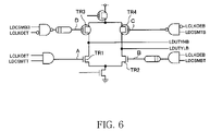
- the logic of the gate circuit that generates the control signals A to D is not limited to that shown in FIG. 1 , and various changes can be performed. Circuits shown in FIG. 6 to FIG. 8 can be taken up as modifications. The circuits shown in FIG. 6 to FIG. 8 perform the same operation as that of the circuit shown in FIG. 1 . However, the circuits shown in FIG. 6 to FIG. 8 increase the number of gate stages from that of the circuit shown in FIG. 1 and generate unbalance in the number of gate stages. Therefore, it is most preferable that the circuit shown in FIG. 1 is used.
- the present invention is not limited thereto, and the invention can be also applied to an n-phase DLL circuit, where n is a power of 2.
Abstract
Description
Claims (18)
Applications Claiming Priority (2)
| Application Number | Priority Date | Filing Date | Title |
|---|---|---|---|
| JP2007-181358 | 2007-07-10 | ||
| JP2007181358A JP4890369B2 (en) | 2007-07-10 | 2007-07-10 | Duty detection circuit, DLL circuit using the same, semiconductor memory device, and data processing system |
Publications (2)
| Publication Number | Publication Date |
|---|---|
| US20090016127A1 US20090016127A1 (en) | 2009-01-15 |
| US7719921B2 true US7719921B2 (en) | 2010-05-18 |
Family
ID=40252969
Family Applications (1)
| Application Number | Title | Priority Date | Filing Date |
|---|---|---|---|
| US12/170,730 Active 2028-10-13 US7719921B2 (en) | 2007-07-10 | 2008-07-10 | Duty detection circuit, DLL circuit using the same, semiconductor memory circuit, and data processing system |
Country Status (2)
| Country | Link |
|---|---|
| US (1) | US7719921B2 (en) |
| JP (1) | JP4890369B2 (en) |
Cited By (3)
| Publication number | Priority date | Publication date | Assignee | Title |
|---|---|---|---|---|
| US20110227619A1 (en) * | 2010-03-19 | 2011-09-22 | Elpida Memory, Inc. | Clock generation circuit, semiconductor device including the same, and method of generating clock signal |
| CN105720949A (en) * | 2014-12-22 | 2016-06-29 | 爱思开海力士有限公司 | Duty cycle detection circuit and method |
| US10727826B2 (en) | 2018-08-14 | 2020-07-28 | Samsung Electronics Co., Ltd. | Delay-locked loop circuit, semiconductor memory device, and methods of operating delay-locked loop circuit |
Families Citing this family (2)
| Publication number | Priority date | Publication date | Assignee | Title |
|---|---|---|---|---|
| JP2007121114A (en) * | 2005-10-28 | 2007-05-17 | Elpida Memory Inc | Duty detecting circuit and dll circuit and semiconductor device equipped therewith |
| JP5642350B2 (en) * | 2009-02-19 | 2014-12-17 | ピーエスフォー ルクスコ エスエイアールエルPS4 Luxco S.a.r.l. | Duty detection circuit, DLL circuit, and semiconductor device |
Citations (14)
| Publication number | Priority date | Publication date | Assignee | Title |
|---|---|---|---|---|
| US6101152A (en) * | 1990-04-18 | 2000-08-08 | Rambus Inc. | Method of operating a synchronous memory device |
| US6166989A (en) * | 1998-07-28 | 2000-12-26 | Mitsubishi Denki Kabushiki Kaisha | Clock synchronous type semiconductor memory device that can switch word configuration |
| US6243320B1 (en) * | 1998-07-29 | 2001-06-05 | Mitsubishi Denki Kabushiki Kaisha | Synchronous semiconductor memory device capable of selecting column at high speed |
| US6262921B1 (en) * | 1997-03-05 | 2001-07-17 | Micron Technology, Inc. | Delay-locked loop with binary-coupled capacitor |
| US6751120B2 (en) * | 1995-01-31 | 2004-06-15 | Renesas Technology Corp. | Clock synchronized non-volatile memory device |
| US6906952B2 (en) * | 1996-07-10 | 2005-06-14 | Renesas Technology Corp. | Nonvolatile semiconductor memory device and data writing method therefor |
| US6947350B2 (en) * | 2001-02-02 | 2005-09-20 | Broadcom Corporation | Synchronous controlled, self-timed local SRAM block |
| JP2006303553A (en) | 2005-04-15 | 2006-11-02 | Elpida Memory Inc | Duty detection circuit and control method thereof |
| US7180790B2 (en) * | 2004-10-21 | 2007-02-20 | Samsung Electronics Co., Ltd. | Non-volatile memory device having controlled bulk voltage and method of programming same |
| JP2007121114A (en) | 2005-10-28 | 2007-05-17 | Elpida Memory Inc | Duty detecting circuit and dll circuit and semiconductor device equipped therewith |
| US7251162B2 (en) * | 2004-04-27 | 2007-07-31 | Renesas Technology Corp. | Nonvolatile memory with multi-frequency charge pump control |
| US7388768B2 (en) * | 2005-02-17 | 2008-06-17 | Hitachi, Ltd. | Semiconductor device |
| US7471569B2 (en) * | 2005-06-15 | 2008-12-30 | Infineon Technologies Ag | Memory having parity error correction |
| US7489580B2 (en) * | 2004-07-16 | 2009-02-10 | Elpida Memory, Inc. | Refresh period generating circuit |
Family Cites Families (2)
| Publication number | Priority date | Publication date | Assignee | Title |
|---|---|---|---|---|
| JP3439670B2 (en) * | 1998-10-15 | 2003-08-25 | 富士通株式会社 | Timing clock generation circuit using hierarchical DLL circuit |
| US6868504B1 (en) * | 2000-08-31 | 2005-03-15 | Micron Technology, Inc. | Interleaved delay line for phase locked and delay locked loops |
-
2007
- 2007-07-10 JP JP2007181358A patent/JP4890369B2/en not_active Expired - Fee Related
-
2008
- 2008-07-10 US US12/170,730 patent/US7719921B2/en active Active
Patent Citations (18)
| Publication number | Priority date | Publication date | Assignee | Title |
|---|---|---|---|---|
| US6101152A (en) * | 1990-04-18 | 2000-08-08 | Rambus Inc. | Method of operating a synchronous memory device |
| US7110322B2 (en) * | 1990-04-18 | 2006-09-19 | Rambus Inc. | Memory module including an integrated circuit device |
| US7286397B2 (en) * | 1995-01-31 | 2007-10-23 | Renesas Technology Corporation | Clock synchronized nonvolatile memory device |
| US6751120B2 (en) * | 1995-01-31 | 2004-06-15 | Renesas Technology Corp. | Clock synchronized non-volatile memory device |
| US6757194B2 (en) * | 1995-01-31 | 2004-06-29 | Renesas Technology Corp. | Clock synchronized non-volatile memory device |
| US6906952B2 (en) * | 1996-07-10 | 2005-06-14 | Renesas Technology Corp. | Nonvolatile semiconductor memory device and data writing method therefor |
| US6262921B1 (en) * | 1997-03-05 | 2001-07-17 | Micron Technology, Inc. | Delay-locked loop with binary-coupled capacitor |
| US6490207B2 (en) * | 1997-03-05 | 2002-12-03 | Micron Technology, Inc. | Delay-locked loop with binary-coupled capacitor |
| US6166989A (en) * | 1998-07-28 | 2000-12-26 | Mitsubishi Denki Kabushiki Kaisha | Clock synchronous type semiconductor memory device that can switch word configuration |
| US6243320B1 (en) * | 1998-07-29 | 2001-06-05 | Mitsubishi Denki Kabushiki Kaisha | Synchronous semiconductor memory device capable of selecting column at high speed |
| US6947350B2 (en) * | 2001-02-02 | 2005-09-20 | Broadcom Corporation | Synchronous controlled, self-timed local SRAM block |
| US7251162B2 (en) * | 2004-04-27 | 2007-07-31 | Renesas Technology Corp. | Nonvolatile memory with multi-frequency charge pump control |
| US7489580B2 (en) * | 2004-07-16 | 2009-02-10 | Elpida Memory, Inc. | Refresh period generating circuit |
| US7180790B2 (en) * | 2004-10-21 | 2007-02-20 | Samsung Electronics Co., Ltd. | Non-volatile memory device having controlled bulk voltage and method of programming same |
| US7388768B2 (en) * | 2005-02-17 | 2008-06-17 | Hitachi, Ltd. | Semiconductor device |
| JP2006303553A (en) | 2005-04-15 | 2006-11-02 | Elpida Memory Inc | Duty detection circuit and control method thereof |
| US7471569B2 (en) * | 2005-06-15 | 2008-12-30 | Infineon Technologies Ag | Memory having parity error correction |
| JP2007121114A (en) | 2005-10-28 | 2007-05-17 | Elpida Memory Inc | Duty detecting circuit and dll circuit and semiconductor device equipped therewith |
Cited By (6)
| Publication number | Priority date | Publication date | Assignee | Title |
|---|---|---|---|---|
| US20110227619A1 (en) * | 2010-03-19 | 2011-09-22 | Elpida Memory, Inc. | Clock generation circuit, semiconductor device including the same, and method of generating clock signal |
| US8299829B2 (en) * | 2010-03-19 | 2012-10-30 | Elpida Memory, Inc. | Clock generation circuit, semiconductor device including the same, and method of generating clock signal |
| CN105720949A (en) * | 2014-12-22 | 2016-06-29 | 爱思开海力士有限公司 | Duty cycle detection circuit and method |
| US9660631B2 (en) * | 2014-12-22 | 2017-05-23 | SK Hynix Inc. | Duty cycle detection circuit and method |
| CN105720949B (en) * | 2014-12-22 | 2020-09-25 | 爱思开海力士有限公司 | Duty cycle detection circuit and method |
| US10727826B2 (en) | 2018-08-14 | 2020-07-28 | Samsung Electronics Co., Ltd. | Delay-locked loop circuit, semiconductor memory device, and methods of operating delay-locked loop circuit |
Also Published As
| Publication number | Publication date |
|---|---|
| JP2009021704A (en) | 2009-01-29 |
| US20090016127A1 (en) | 2009-01-15 |
| JP4890369B2 (en) | 2012-03-07 |
Similar Documents
| Publication | Publication Date | Title |
|---|---|---|
| US8174297B2 (en) | Multi-phase clock generation | |
| KR100557550B1 (en) | Clock synchronization circuit | |
| JP4789172B2 (en) | Delay lock loop and locking method thereof in semiconductor memory device | |
| US20070152680A1 (en) | Duty detection circuit, dll circuit and semiconductor device having same | |
| US10218342B2 (en) | System and method for duty cycle correction | |
| KR100701423B1 (en) | Duty correction device | |
| US7268601B2 (en) | Delay locked loop and clock generation method thereof | |
| US7994834B2 (en) | Duty cycle corrector and clock generator having the same | |
| US20170134014A1 (en) | Duty cycle detector | |
| US7622969B2 (en) | Methods, devices, and systems for a delay locked loop having a frequency divided feedback clock | |
| US7710171B2 (en) | Delayed locked loop circuit | |
| KR20080075286A (en) | Duty cycle correcting circuit and method of controlling the same | |
| US20090058481A1 (en) | Semiconductor memory device and method for driving the same | |
| US20090295442A1 (en) | Apparatus and method for multi-phase clock generation | |
| JP2003069424A (en) | Ring-register controlled delay locked loop and its control method | |
| US20060268655A1 (en) | Method and system for improved efficiency of synchronous mirror delays and delay locked loops | |
| US7719921B2 (en) | Duty detection circuit, DLL circuit using the same, semiconductor memory circuit, and data processing system | |
| KR20220046104A (en) | Duty correction device and method, a semiconductor appratus using the same | |
| KR100525096B1 (en) | DLL circuit | |
| US20080094115A1 (en) | DLL circuit | |
| US8379784B2 (en) | Semiconductor memory device | |
| KR20110030530A (en) | Duty cycle corrector and clock generator including the same | |
| KR20080002590A (en) | Delay locked loop circuit | |
| KR101019985B1 (en) | A delay locked loop circuit and a method of controlling thereof | |
| KR100845808B1 (en) | Clock mismatch correction circuit and dll circuit including the same |
Legal Events
| Date | Code | Title | Description |
|---|---|---|---|
| AS | Assignment |
Owner name: ELPIDA MEMORY, INC., JAPAN Free format text: ASSIGNMENT OF ASSIGNORS INTEREST;ASSIGNORS:KUROKI, KOJI;TAKAI, YASUHIRO;REEL/FRAME:023852/0198 Effective date: 20080620 Owner name: ELPIDA MEMORY, INC.,JAPAN Free format text: ASSIGNMENT OF ASSIGNORS INTEREST;ASSIGNORS:KUROKI, KOJI;TAKAI, YASUHIRO;REEL/FRAME:023852/0198 Effective date: 20080620 |
|
| STCF | Information on status: patent grant |
Free format text: PATENTED CASE |
|
| AS | Assignment |
Owner name: ELPIDA MEMORY INC., JAPAN Free format text: SECURITY AGREEMENT;ASSIGNOR:PS4 LUXCO S.A.R.L.;REEL/FRAME:032414/0261 Effective date: 20130726 |
|
| FPAY | Fee payment |
Year of fee payment: 4 |
|
| AS | Assignment |
Owner name: PS4 LUXCO S.A.R.L., LUXEMBOURG Free format text: ASSIGNMENT OF ASSIGNORS INTEREST;ASSIGNOR:ELPIDA MEMORY, INC.;REEL/FRAME:032899/0588 Effective date: 20130726 |
|
| FEPP | Fee payment procedure |
Free format text: PAYOR NUMBER ASSIGNED (ORIGINAL EVENT CODE: ASPN); ENTITY STATUS OF PATENT OWNER: LARGE ENTITY |
|
| AS | Assignment |
Owner name: PS5 LUXCO S.A.R.L., LUXEMBOURG Free format text: ASSIGNMENT OF ASSIGNORS INTEREST;ASSIGNOR:PS4 LUXCO S.A.R.L.;REEL/FRAME:039818/0506 Effective date: 20130829 Owner name: LONGITUDE SEMICONDUCTOR S.A.R.L., LUXEMBOURG Free format text: CHANGE OF NAME;ASSIGNOR:PS5 LUXCO S.A.R.L.;REEL/FRAME:039793/0880 Effective date: 20131112 |
|
| MAFP | Maintenance fee payment |
Free format text: PAYMENT OF MAINTENANCE FEE, 8TH YEAR, LARGE ENTITY (ORIGINAL EVENT CODE: M1552) Year of fee payment: 8 |
|
| AS | Assignment |
Owner name: LONGITUDE LICENSING LIMITED, IRELAND Free format text: ASSIGNMENT OF ASSIGNORS INTEREST;ASSIGNOR:LONGITUDE SEMICONDUCTOR S.A.R.L.;REEL/FRAME:046867/0248 Effective date: 20180731 |
|
| MAFP | Maintenance fee payment |
Free format text: PAYMENT OF MAINTENANCE FEE, 12TH YEAR, LARGE ENTITY (ORIGINAL EVENT CODE: M1553); ENTITY STATUS OF PATENT OWNER: LARGE ENTITY Year of fee payment: 12 |