US7719510B2 - Flat panel display, display driving apparatus thereof and shift register thereof - Google Patents
Flat panel display, display driving apparatus thereof and shift register thereof Download PDFInfo
- Publication number
- US7719510B2 US7719510B2 US11/429,072 US42907206A US7719510B2 US 7719510 B2 US7719510 B2 US 7719510B2 US 42907206 A US42907206 A US 42907206A US 7719510 B2 US7719510 B2 US 7719510B2
- Authority
- US
- United States
- Prior art keywords
- coupled
- unit
- voltage
- shift register
- control terminal
- Prior art date
- Legal status (The legal status is an assumption and is not a legal conclusion. Google has not performed a legal analysis and makes no representation as to the accuracy of the status listed.)
- Active, expires
Links
- 230000003111 delayed effect Effects 0.000 claims abstract description 9
- 239000003990 capacitor Substances 0.000 claims description 14
- 238000010586 diagram Methods 0.000 description 16
- 239000000758 substrate Substances 0.000 description 4
- 239000011521 glass Substances 0.000 description 3
- 229910021420 polycrystalline silicon Inorganic materials 0.000 description 3
- 229920005591 polysilicon Polymers 0.000 description 3
- 239000004973 liquid crystal related substance Substances 0.000 description 2
- 230000004048 modification Effects 0.000 description 2
- 238000012986 modification Methods 0.000 description 2
- LKJPSUCKSLORMF-UHFFFAOYSA-N Monolinuron Chemical compound CON(C)C(=O)NC1=CC=C(Cl)C=C1 LKJPSUCKSLORMF-UHFFFAOYSA-N 0.000 description 1
- 230000000694 effects Effects 0.000 description 1
- 230000005855 radiation Effects 0.000 description 1
- 239000010409 thin film Substances 0.000 description 1
- 230000003867 tiredness Effects 0.000 description 1
- 208000016255 tiredness Diseases 0.000 description 1
Images


Classifications
-
- G—PHYSICS
- G09—EDUCATION; CRYPTOGRAPHY; DISPLAY; ADVERTISING; SEALS
- G09G—ARRANGEMENTS OR CIRCUITS FOR CONTROL OF INDICATING DEVICES USING STATIC MEANS TO PRESENT VARIABLE INFORMATION
- G09G3/00—Control arrangements or circuits, of interest only in connection with visual indicators other than cathode-ray tubes
- G09G3/20—Control arrangements or circuits, of interest only in connection with visual indicators other than cathode-ray tubes for presentation of an assembly of a number of characters, e.g. a page, by composing the assembly by combination of individual elements arranged in a matrix no fixed position being assigned to or needed to be assigned to the individual characters or partial characters
-
- G—PHYSICS
- G11—INFORMATION STORAGE
- G11C—STATIC STORES
- G11C19/00—Digital stores in which the information is moved stepwise, e.g. shift registers
- G11C19/18—Digital stores in which the information is moved stepwise, e.g. shift registers using capacitors as main elements of the stages
- G11C19/182—Digital stores in which the information is moved stepwise, e.g. shift registers using capacitors as main elements of the stages in combination with semiconductor elements, e.g. bipolar transistors, diodes
- G11C19/184—Digital stores in which the information is moved stepwise, e.g. shift registers using capacitors as main elements of the stages in combination with semiconductor elements, e.g. bipolar transistors, diodes with field-effect transistors, e.g. MOS-FET
-
- G—PHYSICS
- G09—EDUCATION; CRYPTOGRAPHY; DISPLAY; ADVERTISING; SEALS
- G09G—ARRANGEMENTS OR CIRCUITS FOR CONTROL OF INDICATING DEVICES USING STATIC MEANS TO PRESENT VARIABLE INFORMATION
- G09G2300/00—Aspects of the constitution of display devices
- G09G2300/04—Structural and physical details of display devices
- G09G2300/0404—Matrix technologies
- G09G2300/0408—Integration of the drivers onto the display substrate
-
- G—PHYSICS
- G09—EDUCATION; CRYPTOGRAPHY; DISPLAY; ADVERTISING; SEALS
- G09G—ARRANGEMENTS OR CIRCUITS FOR CONTROL OF INDICATING DEVICES USING STATIC MEANS TO PRESENT VARIABLE INFORMATION
- G09G2310/00—Command of the display device
- G09G2310/02—Addressing, scanning or driving the display screen or processing steps related thereto
- G09G2310/0264—Details of driving circuits
- G09G2310/0267—Details of drivers for scan electrodes, other than drivers for liquid crystal, plasma or OLED displays
-
- G—PHYSICS
- G09—EDUCATION; CRYPTOGRAPHY; DISPLAY; ADVERTISING; SEALS
- G09G—ARRANGEMENTS OR CIRCUITS FOR CONTROL OF INDICATING DEVICES USING STATIC MEANS TO PRESENT VARIABLE INFORMATION
- G09G2310/00—Command of the display device
- G09G2310/02—Addressing, scanning or driving the display screen or processing steps related thereto
- G09G2310/0264—Details of driving circuits
- G09G2310/0275—Details of drivers for data electrodes, other than drivers for liquid crystal, plasma or OLED displays, not related to handling digital grey scale data or to communication of data to the pixels by means of a current
Definitions
- the present invention relates to a shift register. More particularly, the present invention relates to a flat panel display, a display driving apparatus thereof and a shift register thereof.
- the flat panel display for example, liquid crystal display (LCD)
- LCD liquid crystal display
- the flat panel display has such characteristics as being light, thin, small, low radiation and power saving, these features help save the space usage of office or home, and reduce the feeling of eye tiredness after a long time viewing. Therefore, the flat panel display has characteristic to fully substitute the conventional cathode ray tube (CRT).
- CTR cathode ray tube
- FIG. 1A is a circuit diagram of a conventional shift register, which is implemented upon a glass substrate using low temperature poly silicon (LTPS) technology.
- the shift register can be adapted for the driving circuit of the flat panel display, for example, the gate driver for vertical scan of the liquid crystal display.
- FIG. 1A includes 5 stages of same shift registers, SR 1 , SR 2 , SR 3 , SR 4 , and SR 5 , respectively.
- Each shift register includes an input terminal In, clock signal input terminals CKA and CKB and an output terminal Out.
- FIG. 1A includes four clock signal wires respectively inputting a first clock signal CK 1 , a second clock signal CK 2 , a third clock signal CK 3 and a fourth clock signal CK 4 .
- FIG. 1A also includes a start pulse wire SP.
- FIG. 1B is a detailed circuit diagram of the conventional shift register SR 1 in FIG. 1A , which is implemented upon a glass substrate using the low temperature poly silicon (LTPS) technology.
- the circuit comprises thin film transistors (TFT) 101 , 102 , 103 and a capacitor 104 .
- the first source/drain of the TFT 101 is the input terminal In of the SR 1 .
- the second source/drain of the TFT 101 is coupled to the gate of the TFT 102 .
- the gate of the TFT 101 is the clock signal input terminal CKA, and the gate of the TFT 101 is coupled to the gate of the TFT 103 .
- the first source/drain of the TFT 102 is the clock signal input terminal CKB.
- the second source/drain of the TFT 102 is the output terminal Out of the SR 1 .
- the first source/drain of the TFT 103 is coupled to the second source/drain of the TFT 102 .
- the second source/drain of the TFT 103 is the low level voltage input terminal VSS.
- FIG. 1C is a clock diagram of the circuit in FIG. 1A .
- VSS low level of the voltage amplitude of the clock signal
- VDD high level of the voltage amplitude of the clock signal
- VDD high level voltage
- the clock signal CK 3 When the clock signal CK 1 turns to low level from high level, the clock signal CK 3 also turns to high level from low level at the same time. As the capacitor 104 stores the high level voltage, the gate of the TFT 102 receives the high level voltage so that the high level voltage VDD on the clock signal CK 3 is conducted to the output terminal Out. Accordingly, the next shift register SR 2 starts to receive the high level voltage output from the output terminal Out.
- the conventional technology has provided an architecture of shift registers, however, the architecture has one disadvantage.
- the clock signal CKB must be input from the source/drain of the TFT 102 . Accordingly, the clock signal generator should have very strong driving power; however, the increase of the driving power would cause the increase of the layout area.
- the present invention is directed to provide a shift register, used to reduce the required driving power of the chip in providing the clock signal.
- Another aspect of the present invention is to provide a display driving apparatus, used to reduce the layout area of the chip.
- Another aspect of the present invention is to provide a flat panel display to reduce the cost.
- the present invention provides a shift register, adapted for driving a flat panel display.
- the shift register receives an input signal and a clock signal.
- the shift register includes a delay unit and a buffer unit.
- the delay unit is used to delay the input signal for half period of the clock signal and then output the delayed input signal.
- the buffer unit receives the output signal of the delay unit, and provides an extra driving power accordingly. Wherein, the buffer unit is operated by a fixed first voltage and a fixed second voltage.
- the delay unit comprises a first switching unit, a charge storing unit and a second switching unit.
- the first switching unit comprises a first end and a second end, wherein the first end is the input terminal of the delay unit.
- the clock signal it is determined whether to conduct the circuit between the first end and the second end.
- One end of the charge storing unit is coupled to the first voltage, and the other end is coupled to the second end.
- the second switching unit comprises a third end and a fourth end, wherein the third end is coupled to the second end, and the fourth end is the output terminal of the delay unit. According to the reversed signal of the clock signal, it is determined whether to conduct the circuit between the third end and the fourth end.
- the buffer unit comprises a third switching unit and a fourth switching unit.
- the third switching unit comprises a first control terminal, a fifth end and a sixth end, wherein the first control terminal is coupled to the fourth end, and the fifth end is coupled to the second voltage.
- the fourth switching unit comprises a second control terminal, a seventh end and an eighth end, wherein the second control terminal is coupled to the clock signal, and the seventh end is coupled to the sixth end, and the eighth end is coupled to the first voltage.
- the present invention further provides a display driving apparatus comprising N shift registers, and each shift register comprises an input node, an output node, a delay unit and a buffer unit.
- An input terminal of the delay unit is coupled to the input node, and the delay unit is used to delay a signal on the input node for half period or the clock signal and then output the delayed signal.
- An output terminal of the buffer unit is coupled to the output node, and the buffer unit is used to receive an output signal of the delay unit, and provide an extra driving power accordingly.
- N is a nature integer
- the input node of the Nth shift register is coupled to the output node of the N ⁇ 1th shift register.
- the buffer unit is operated by a fixed first voltage and a fixed second voltage.
- the present invention further provides a flat panel display, comprising a display driving apparatus and a display panel.
- the display driving apparatus comprises N shift registers, and each shift register has an input node, an output node, a delay unit and a buffer unit.
- An input terminal of the delay unit is coupled to the input node, and the delay unit is used to delay a signal on the input node for half period of the clock signal and then output the delayed signal.
- An output terminal of the buffer unit is coupled to the output node, and the buffer unit is used to receive an output signal of the delay unit and provide an extra driving power accordingly.
- N is a nature integer
- the input node of the Nth shift register is coupled to the output node of the N ⁇ 1th shift register.
- the buffer unit is operated by a fixed first voltage and a fixed second voltage.
- the display panel receives data for the signals on the output nodes of the display driving apparatus for displaying image.
- the delay unit applies a fixed voltage supply and the clock signal is only needed to be provided to the gate of the transistor, the load for the clock signal is small. Therefore, the clock signal does not need too much driving power to operate the shift register normally, so that the volume of the clock generator can be reduced, therefore, the layout area of the clock generator and the cost can be reduced.
- FIG. 1A is a circuit diagram of a conventional shift register, which is implemented upon a glass substrate using low temperature poly silicon (LTPS) technology.
- LTPS low temperature poly silicon
- FIG. 1B is a detailed circuit diagram of the conventional shift register SR 1 in FIG. 1A .
- FIG. 1C is an operation waveform of the conventional circuit in FIG. 1A .
- FIG. 2A is a block diagram of the flat panel display circuit according to one embodiment of the present invention.
- FIG. 2B is a diagram of the display driving apparatus according to one embodiment of the present invention.
- FIG. 2C is a circuit diagram of the shift register according to one embodiment of the present invention.
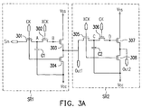
- FIG. 3A is a circuit diagram of the shift register according to one embodiment of the present invention.
- FIG. 3B is an operation waveform of the shift register circuit in FIG. 3A according to one embodiment of the present invention.
- FIG. 4 is a circuit diagram of the shift register according to one embodiment of the present invention.
- FIG. 5 is a circuit diagram of the shift register according to one embodiment of the present invention.
- FIG. 6 is a circuit diagram of the shift register according to one embodiment of the present invention.
- FIG. 7 is a circuit diagram of the shift register according to one embodiment of the present invention.
- FIG. 8 is a circuit diagram of the shift register according to one embodiment of the present invention.
- FIG. 9A is a circuit diagram of the shift register according to one embodiment of the present invention.
- FIG. 9B is a circuit diagram of the shift register according to one embodiment of the present invention.
- the present invention provides a flat panel display, as shown in FIG. 2A , and the flat panel display comprises a display panel 20 and display driving apparatuses 22 A and 22 B.
- the display driving apparatuses 22 A or 22 B are coupled to the substrate of display panel 20 , used for driving the panel to display image.
- the detailed circuit of the display driving apparatus 22 A is shown in FIG. 2B .
- the driving apparatus comprises a plurality of shift registers SR, and each shift register SR also comprises a delay unit Delay and a buffer unit Buffer.
- the detailed circuit of the shift register SR is shown in FIG. 2C .
- the circuit can be divided into two portions: the first portion is a delay unit 200 , and the second portion is a buffer unit 210 .
- the first portion is a delay unit 200
- the second portion is a buffer unit 210 .
- Sin is an input node
- CK and XCK are clock signals reversed to each other
- the high level voltage Vcc and the low level voltage Vss are fixed voltage source.
- the function of the delay unit 200 is to delay the input signal on the input node Sin for a half period of the clock signal and then output the delayed input signal.
- the buffer unit 210 receives the output signal of the delay unit 200 , i.e., the signal of the node b, and provides an extra driving power on the output node Out in accordance to the received output signal.
- the buffer unit 210 is operated by fixed voltages Vcc and Vss.
- the clock signal CKB is applied on the source/drain gate of the transistor 102 .
- the shift register provided by the present invention uses four transistors in total: the delay unit 200 uses two transistors 201 , 202 and a charge storing unit Cap (capacitor) to simple and hold; and the buffer unit 210 uses two transistors 211 and 212 to output the extra driving power.
- FIG. 3A and FIG. 3B the operation waveform, simultaneously.
- the single shift register architecture in FIG. 2C is revised to two shift registers of FIG. 2B , SR 1 and SR 2 , as shown in FIG. 3A .
- FIG. 3A includes eight P type transistors, 301 , 302 , 303 , 304 , 305 , 306 , 307 , and 308 .
- FIG. 3A also includes two capacitors, C 1 and C 2 .
- several nodes are marked in FIG. 3A , i.e., the input node Sin, node A, node B, node C, node D, output nodes Out 1 and Out 2 .
- the clock signal CK and XCK are respectively added on the delay unit of each shift registers SR 1 , SR 2 .
- the high level voltage Vcc and the low level voltage Vss are respectively fixed voltage sources.
- the clock signal CK also begins to turn to low level voltage from high level voltage
- the clock signal XCK begins to turn to high level voltage from low level voltage.
- the gate of the transistor 301 receives a low level voltage and the transistor 301 begins to be conducted
- the gate of the transistor 302 receives a high level voltage so that the transistor 302 is turned off.
- the capacitor C 1 is discharged into low level voltage through the transistor 301 .
- the gate of the transistor 304 in the buffer unit also receives the low level voltage of the clock signal CK so that the transistor 304 is conducted. Accordingly, the output node Out 1 maintains at high level voltage.
- the other clock signal XCK also begins to turn to low level voltage from high level voltage.
- the transistor 301 is turned off, and the transistor 302 is conducted, and the high level voltage at the node B begins to be discharge through the capacitor at the node A, so that the gate of the transistor 303 receives a low level voltage, and at this time, the transistor 303 begins to be conducted.
- the clock signal CK is at high level voltage at this time so as to turn off the transistor 304 , the data (low level voltage) stored at the node A is output to the output node Out 1 through the transistors 303 and 304 of the buffer unit.
- the transistor 305 begins to be conducted, and the output node begins to be discharged through the capacitor C 2 at the node C.
- the capacitor C 2 stores the data (low level voltage) output from the shift register SR 1 , and the gate of the transistor 306 is at high level voltage when coupled to the clock signal CK, so that the transistor 306 is turned off.
- the data (low level voltage) is held in the capacitor C 2 .
- the gate of the transistor 308 in the buffer unit also receives the low level voltage of the clock signal XCK so that the transistor 308 is conducted and the output node Out 2 is maintained at high level voltage.
- the other clock signal CK When the clock signal XCK begins to turn to high level voltage form low level voltage, the other clock signal CK also begins to turn to low level voltage from high level voltage. At this time, the transistor 305 is turned off, and the transistor 306 is conducted, and the high level voltage at the node D begins to be discharged through the capacitor at the node C, so that the gate of the transistor 307 receives a low level voltage, and at this time, the transistor 307 begins to be conducted. As the clock signal XCK is at high level voltage at this time so as to turn off the transistor 308 , the data (low level voltage) stored at the node C is output to the output node Out 2 through the transistors 307 and 308 of the buffer unit. Therefore, the data (low level voltage) can be transferred stage by stage by repeating the above operations.
- the above embodiment is just an example, and there are still many embodiments.
- all of the transistors are changed to N type transistors, and the original low level voltage Vss and high level voltage Vcc are replaced by each other, and the operation modes thereof are almost the same, and readers can deduce them by themselves.
- the present invention can still applies the embodiment of CMOS, as shown in FIG. 5 and FIG. 6 , and the operation modes are almost the same, and readers can deduce them by themselves.
- FIG. 2B can still be changed to the embodiment as shown in FIG. 7 .
- the capacitor in FIG. 7 originally coupled to Vcc, is changed to be coupled to a reference voltage Vref, and the operation theory is the same, so that the detail is omitted here.
- FIG. 8 describes another implementation mode of the embodiment of the present invention. The difference between FIG. 8 and FIG. 2B is that the gate of the transistor 212 of the buffer unit 210 in FIG. 2B is coupled to the clock signal CK, the gate of the transistor 812 of the buffer unit 810 in FIG. 8 is coupled to the output of an inverter INV, and the input of the inverter INV is coupled to the output of the delay unit 800 ; the operation is similar to that in FIG. 2B , so that the detail is omitted here.
- FIG. 9A and FIG. 9B describe an implementation of the embodiment of the present invention.
- the difference between FIG. 9A and FIG. 7 is that there is one more switching unit 900 in FIG. 9A than FIG. 7 .
- the circuit in the embodiment in FIG. 9A , implemented in FIG. 9B is, for example, SR 1 .
- the output of SR 1 is Out 1
- the next stage of the shift register SR 1 is the shift register SR 2 and output thereof is Out 2
- the further next stage output is Out 3 .
- the control terminal of the control switching unit 900 must be coupled to the output Out 3 .
- the implementation of the embodiment further provides more stable output voltage.
- FIG. 8A , FIGS. 9A , and 9 B can be implemented by N-type or P-type transistors, or by the CMOS transistors. The detail is not further described here.
- the delay unit applies fixed voltage Source in the present invention and all of the clock signals are driving gates, the load effect output from the clock signal can be reduced. Besides, the layout area is reduced to lower the cost, and the change of the clock signal voltage will not affect the output terminal so that the voltage vibration of the output terminal is reduced.
Abstract
Description
Claims (19)
Applications Claiming Priority (3)
| Application Number | Priority Date | Filing Date | Title |
|---|---|---|---|
| TW94126158A | 2005-08-02 | ||
| TW094126158A TWI304199B (en) | 2005-08-02 | 2005-08-02 | Flat panel display, display driving apparatus thereof and shift register thereof |
| TW94126158 | 2005-08-02 |
Publications (2)
| Publication Number | Publication Date |
|---|---|
| US20070030239A1 US20070030239A1 (en) | 2007-02-08 |
| US7719510B2 true US7719510B2 (en) | 2010-05-18 |
Family
ID=37717199
Family Applications (1)
| Application Number | Title | Priority Date | Filing Date |
|---|---|---|---|
| US11/429,072 Active 2029-03-18 US7719510B2 (en) | 2005-08-02 | 2006-05-05 | Flat panel display, display driving apparatus thereof and shift register thereof |
Country Status (2)
| Country | Link |
|---|---|
| US (1) | US7719510B2 (en) |
| TW (1) | TWI304199B (en) |
Cited By (4)
| Publication number | Priority date | Publication date | Assignee | Title |
|---|---|---|---|---|
| US20080316195A1 (en) * | 2007-06-21 | 2008-12-25 | Chunghwa Picture Tubes, Ltd. | Gate driving circuit and power control circuit |
| US20100103184A1 (en) * | 2008-10-24 | 2010-04-29 | Chih-Ping Chen | Driving Circuit for Detecting Line Short defects |
| US20130009925A1 (en) * | 2010-04-16 | 2013-01-10 | Nobuyoshi Ueda | Display panel |
| CN106548740A (en) * | 2016-12-02 | 2017-03-29 | 京东方科技集团股份有限公司 | Shift register circuit and its driving method, gate driver circuit and display device |
Families Citing this family (5)
| Publication number | Priority date | Publication date | Assignee | Title |
|---|---|---|---|---|
| JP3872085B2 (en) * | 2005-06-14 | 2007-01-24 | シャープ株式会社 | Display device drive circuit, pulse generation method, and display device |
| TWI366177B (en) * | 2007-08-08 | 2012-06-11 | Au Optronics Corp | Lcd display with a gate driver outputting non-overlapping scanning signals |
| TWI371741B (en) * | 2007-12-12 | 2012-09-01 | Hannstar Display Corp | Driving signal generating circuit and signal generatiing method thereof |
| TWI397259B (en) | 2010-05-10 | 2013-05-21 | Au Optronics Corp | Shift register circuit |
| CN110827741B (en) * | 2019-11-19 | 2023-04-18 | 京东方科技集团股份有限公司 | Output buffer circuit, drive circuit and display device |
Citations (5)
| Publication number | Priority date | Publication date | Assignee | Title |
|---|---|---|---|---|
| US5956011A (en) * | 1995-10-14 | 1999-09-21 | Semiconductor Energy Laboratory Co., Ltd. | Matrix type liquid-crystal display unit |
| US6373458B1 (en) * | 1998-11-04 | 2002-04-16 | Matsushita Electric Industrial Co., Ltd. | Motion circuit and on-board driver circuit for liquid crystal display panel employing the motion circuit |
| US20040085284A1 (en) * | 2002-10-31 | 2004-05-06 | Toppoly Optoelectronics Corp. | Scan driving circuit for use in planar display |
| US7068246B2 (en) * | 2000-06-12 | 2006-06-27 | Semiconductor Energy Laboratory Co., Ltd. | Light emitting module and method of driving the same, and optical sensor |
| US7158128B2 (en) * | 2001-08-28 | 2007-01-02 | Sharp Kabushiki Kaisha | Drive unit and display module including same |
-
2005
- 2005-08-02 TW TW094126158A patent/TWI304199B/en not_active IP Right Cessation
-
2006
- 2006-05-05 US US11/429,072 patent/US7719510B2/en active Active
Patent Citations (5)
| Publication number | Priority date | Publication date | Assignee | Title |
|---|---|---|---|---|
| US5956011A (en) * | 1995-10-14 | 1999-09-21 | Semiconductor Energy Laboratory Co., Ltd. | Matrix type liquid-crystal display unit |
| US6373458B1 (en) * | 1998-11-04 | 2002-04-16 | Matsushita Electric Industrial Co., Ltd. | Motion circuit and on-board driver circuit for liquid crystal display panel employing the motion circuit |
| US7068246B2 (en) * | 2000-06-12 | 2006-06-27 | Semiconductor Energy Laboratory Co., Ltd. | Light emitting module and method of driving the same, and optical sensor |
| US7158128B2 (en) * | 2001-08-28 | 2007-01-02 | Sharp Kabushiki Kaisha | Drive unit and display module including same |
| US20040085284A1 (en) * | 2002-10-31 | 2004-05-06 | Toppoly Optoelectronics Corp. | Scan driving circuit for use in planar display |
Cited By (8)
| Publication number | Priority date | Publication date | Assignee | Title |
|---|---|---|---|---|
| US20080316195A1 (en) * | 2007-06-21 | 2008-12-25 | Chunghwa Picture Tubes, Ltd. | Gate driving circuit and power control circuit |
| US7839398B2 (en) * | 2007-06-21 | 2010-11-23 | Chunghwa Picture Tubes, Ltd. | Gate driving circuit and power control circuit |
| US20100103184A1 (en) * | 2008-10-24 | 2010-04-29 | Chih-Ping Chen | Driving Circuit for Detecting Line Short defects |
| US8248356B2 (en) * | 2008-10-24 | 2012-08-21 | Au Optronics Corp. | Driving circuit for detecting line short defects |
| US20130009925A1 (en) * | 2010-04-16 | 2013-01-10 | Nobuyoshi Ueda | Display panel |
| US9208741B2 (en) * | 2010-04-16 | 2015-12-08 | Sharp Kabushiki Kaisha | Display panel |
| CN106548740A (en) * | 2016-12-02 | 2017-03-29 | 京东方科技集团股份有限公司 | Shift register circuit and its driving method, gate driver circuit and display device |
| US10490295B2 (en) | 2016-12-02 | 2019-11-26 | Boe Technology Group Co., Ltd. | Shift register circuit and driving method, gate driver circuit, and display apparatus |
Also Published As
| Publication number | Publication date |
|---|---|
| US20070030239A1 (en) | 2007-02-08 |
| TW200707359A (en) | 2007-02-16 |
| TWI304199B (en) | 2008-12-11 |
Similar Documents
| Publication | Publication Date | Title |
|---|---|---|
| US7719510B2 (en) | Flat panel display, display driving apparatus thereof and shift register thereof | |
| US10685616B2 (en) | Shift register circuit, method for driving the same, gate drive circuit, and display panel | |
| US7978809B2 (en) | Shift register of a display device | |
| US7734003B2 (en) | Shift register arrays | |
| US8054935B2 (en) | Shift register with low power consumption | |
| US9640276B2 (en) | Shift register unit and gate driving circuit | |
| US8422620B2 (en) | Shift registers | |
| US7590214B2 (en) | Shift register and shift register apparatus thereof | |
| US7656194B2 (en) | Shift register circuit | |
| CN110619852B (en) | Scanning circuit, display panel and display device | |
| US20100245298A1 (en) | Shift register capable of reducing coupling effect | |
| WO2020098309A1 (en) | Shift register and drive method therefor, gate drive circuit, array substrate, and display device | |
| JP2016526247A (en) | Shift register unit and display device | |
| US20050156858A1 (en) | Driving circuit of liquid crystal display | |
| US7292218B2 (en) | Shift-register circuit | |
| US20220319370A1 (en) | Goa circuit and display panel | |
| US20100290581A1 (en) | Shift Registers | |
| US7499517B2 (en) | Shift register and shift register set using the same | |
| US7471122B2 (en) | Shift register | |
| CN112542198A (en) | Shift register and display panel | |
| TWI415060B (en) | Image display systems | |
| US11043177B2 (en) | Shift register | |
| US7274625B1 (en) | Display device | |
| US20060028461A1 (en) | Shift register and display panel utilizing same | |
| CN112397010A (en) | Shift register and driving method thereof, display panel and display device |
Legal Events
| Date | Code | Title | Description |
|---|---|---|---|
| AS | Assignment |
Owner name: CHI MEI EL CORPORATION,TAIWAN Free format text: ASSIGNMENT OF ASSIGNORS INTEREST;ASSIGNORS:GUO, HONG-RU;HUANG, CHIEN-HSIANG;TSENG, MING-CHUN;REEL/FRAME:017843/0277 Effective date: 20060223 Owner name: CHI MEI OPTOELECTRONICS CORPORATION,TAIWAN Free format text: ASSIGNMENT OF ASSIGNORS INTEREST;ASSIGNORS:GUO, HONG-RU;HUANG, CHIEN-HSIANG;TSENG, MING-CHUN;REEL/FRAME:017843/0277 Effective date: 20060223 Owner name: CHI MEI EL CORPORATION, TAIWAN Free format text: ASSIGNMENT OF ASSIGNORS INTEREST;ASSIGNORS:GUO, HONG-RU;HUANG, CHIEN-HSIANG;TSENG, MING-CHUN;REEL/FRAME:017843/0277 Effective date: 20060223 Owner name: CHI MEI OPTOELECTRONICS CORPORATION, TAIWAN Free format text: ASSIGNMENT OF ASSIGNORS INTEREST;ASSIGNORS:GUO, HONG-RU;HUANG, CHIEN-HSIANG;TSENG, MING-CHUN;REEL/FRAME:017843/0277 Effective date: 20060223 |
|
| STCF | Information on status: patent grant |
Free format text: PATENTED CASE |
|
| AS | Assignment |
Owner name: CHIMEI INNOLUX CORPORATION,TAIWAN Free format text: MERGER;ASSIGNOR:CHI MEI OPTOELECTRONICS CORP.;REEL/FRAME:024358/0238 Effective date: 20100318 Owner name: CHIMEI INNOLUX CORPORATION, TAIWAN Free format text: MERGER;ASSIGNOR:CHI MEI OPTOELECTRONICS CORP.;REEL/FRAME:024358/0238 Effective date: 20100318 |
|
| FPAY | Fee payment |
Year of fee payment: 4 |
|
| AS | Assignment |
Owner name: INNOLUX CORPORATION, TAIWAN Free format text: CHANGE OF NAME;ASSIGNOR:CHIMEI INNOLUX CORPORATION;REEL/FRAME:032621/0718 Effective date: 20121219 |
|
| MAFP | Maintenance fee payment |
Free format text: PAYMENT OF MAINTENANCE FEE, 8TH YEAR, LARGE ENTITY (ORIGINAL EVENT CODE: M1552) Year of fee payment: 8 |
|
| MAFP | Maintenance fee payment |
Free format text: PAYMENT OF MAINTENANCE FEE, 12TH YEAR, LARGE ENTITY (ORIGINAL EVENT CODE: M1553); ENTITY STATUS OF PATENT OWNER: LARGE ENTITY Year of fee payment: 12 |