US7714562B2 - Hysteretic switching regulator - Google Patents
Hysteretic switching regulator Download PDFInfo
- Publication number
- US7714562B2 US7714562B2 US11/633,635 US63363506A US7714562B2 US 7714562 B2 US7714562 B2 US 7714562B2 US 63363506 A US63363506 A US 63363506A US 7714562 B2 US7714562 B2 US 7714562B2
- Authority
- US
- United States
- Prior art keywords
- coupled
- switching regulator
- terminal
- low
- circuit
- Prior art date
- Legal status (The legal status is an assumption and is not a legal conclusion. Google has not performed a legal analysis and makes no representation as to the accuracy of the status listed.)
- Expired - Fee Related, expires
Links
- 239000003990 capacitor Substances 0.000 claims description 16
- 238000013016 damping Methods 0.000 claims description 16
- 238000005070 sampling Methods 0.000 claims description 5
- 230000008878 coupling Effects 0.000 claims description 3
- 238000010168 coupling process Methods 0.000 claims description 3
- 238000005859 coupling reaction Methods 0.000 claims description 3
- 230000008859 change Effects 0.000 claims description 2
- 230000004044 response Effects 0.000 description 10
- 230000008901 benefit Effects 0.000 description 9
- 230000006870 function Effects 0.000 description 9
- 230000001052 transient effect Effects 0.000 description 3
- 230000001276 controlling effect Effects 0.000 description 2
- 230000009467 reduction Effects 0.000 description 2
- 239000000919 ceramic Substances 0.000 description 1
- 230000000694 effects Effects 0.000 description 1
- 238000004146 energy storage Methods 0.000 description 1
- 230000010354 integration Effects 0.000 description 1
- 230000003993 interaction Effects 0.000 description 1
- 230000004048 modification Effects 0.000 description 1
- 238000012986 modification Methods 0.000 description 1
- 230000008520 organization Effects 0.000 description 1
- 230000001105 regulatory effect Effects 0.000 description 1
- 229910052715 tantalum Inorganic materials 0.000 description 1
- GUVRBAGPIYLISA-UHFFFAOYSA-N tantalum atom Chemical compound [Ta] GUVRBAGPIYLISA-UHFFFAOYSA-N 0.000 description 1
Images


Classifications
-
- H—ELECTRICITY
- H02—GENERATION; CONVERSION OR DISTRIBUTION OF ELECTRIC POWER
- H02M—APPARATUS FOR CONVERSION BETWEEN AC AND AC, BETWEEN AC AND DC, OR BETWEEN DC AND DC, AND FOR USE WITH MAINS OR SIMILAR POWER SUPPLY SYSTEMS; CONVERSION OF DC OR AC INPUT POWER INTO SURGE OUTPUT POWER; CONTROL OR REGULATION THEREOF
- H02M3/00—Conversion of dc power input into dc power output
- H02M3/02—Conversion of dc power input into dc power output without intermediate conversion into ac
- H02M3/04—Conversion of dc power input into dc power output without intermediate conversion into ac by static converters
- H02M3/10—Conversion of dc power input into dc power output without intermediate conversion into ac by static converters using discharge tubes with control electrode or semiconductor devices with control electrode
- H02M3/145—Conversion of dc power input into dc power output without intermediate conversion into ac by static converters using discharge tubes with control electrode or semiconductor devices with control electrode using devices of a triode or transistor type requiring continuous application of a control signal
- H02M3/155—Conversion of dc power input into dc power output without intermediate conversion into ac by static converters using discharge tubes with control electrode or semiconductor devices with control electrode using devices of a triode or transistor type requiring continuous application of a control signal using semiconductor devices only
- H02M3/156—Conversion of dc power input into dc power output without intermediate conversion into ac by static converters using discharge tubes with control electrode or semiconductor devices with control electrode using devices of a triode or transistor type requiring continuous application of a control signal using semiconductor devices only with automatic control of output voltage or current, e.g. switching regulators
- H02M3/1563—Conversion of dc power input into dc power output without intermediate conversion into ac by static converters using discharge tubes with control electrode or semiconductor devices with control electrode using devices of a triode or transistor type requiring continuous application of a control signal using semiconductor devices only with automatic control of output voltage or current, e.g. switching regulators without using an external clock
Definitions
- the present invention relates to an improved hysteretic switching regulator, and more specifically, to a novel, cost effective design for a hysteretic switching regulator in which the control signal for controlling the switching function of the regulator is independent from variations regarding the operation of the device, such as variations in load current.
- FIG. 1 a illustrates an example of a prior art hysteretic regulator. As explained in more detail below, in this circuit, the equivalent series resistance of the output capacitor is utilized to generate the control ramp signal which is supplied to the hysteresis comparator.
- the inherent triangular waveform of the inductor current I L flowing through the inductor 15 generated by the turning on and off of the high and low side switches 11 , 12 , which operate out of phase with one another, causes a ripple voltage (shown in FIG. 1 b ) to be developed across the equivalent series resistance (ESR) of the output capacitor C, 13 .
- This ripple voltage is applied to the hysteresis comparator 16 , causing the comparator 16 to turn on and off, thereby creating the switching control signal, which is coupled to high and low side switches 11 , 12 .
- the configuration of the switching regulator shown in FIG. 1 a requires a ripple voltage to appear on the output load 17 , which is clearly undesirable and cannot be tolerated in the supply voltage of many systems.
- ESR equivalent series resistor
- FIGS. 2 a and 2 b illustrate additional prior art hysteretic switching regulators which attempt to solve some of the shortcomings of the switching regulator shown in FIG. 1 a .
- a current sense resistor 19 is placed ahead of the load capacitor 13 .
- the inductor current I L flowing through the small value current sense resistor R S 19 produces the required ramp control signal, which is coupled to the input of the hysteresis comparator 16 .
- the DC voltage at the load 17 does not equal the DC voltage at the sampling point for generating the control signal, and therefore an error is introduced into the control signal, which causes an error in the regulated output voltage, V OUT .
- I L I L ⁇ ⁇ V L ⁇ ( t ) ⁇ d t . This is typically done with an R-C low pass filter approximation to an integrator as shown in FIG. 3 , which illustrates yet another prior art configuration of a hysteretic switching regulator.
- the R I —C I network 25 implements a low pass filter that effectively integrates the inductor voltage to obtain an inductor current signal that can be used for the ramp control signal, which is coupled to the hysteresis comparator 16 .
- C C 21 and resistor 22 can be added as in the device of FIG. 2 b to reduce the effect of the inherent series resistance of the inductor (r L ) on V OUT , but it cannot be eliminated from the integration. While the configuration illustrated in FIG. 3 helps reduce the error in V OUT associated with the series resistance, Rs, in the switching regulator configuration of FIG. 2 , as more components are required, including energy storage elements (i.e., inductors and capacitors), the switching regulator of FIG. 3 exhibits a poor transient response and becomes prohibitively costly, because the required component values cannot be easily implemented within an integrated circuit.
- a primary objective of the present invention to provide a switching regulator that eliminates the problems associated with prior art devices as discussed above. More specifically, one objective is to provide a switching regulator which generates the control signal without utilizing a resistor to sense the inductor current and who's amplitude is independent of the magnitude of the load current. By achieving the foregoing objective, it is possible to produce a hysteretic switching regulator that overcomes the problems noted above with the prior art devices.
- the present invention relates to a switching regulator circuit including a high-side switch and a low-side switch; an inductor having a first terminal coupled to a common terminal between the high-side switch and the low-side switch, and a second terminal coupled to an output terminal of the switching regulator circuit; a low-pass filter coupled to the first terminal of the inductor, which is operative for generating a ramp signal based on the voltage signal present at the first terminal of the inductor; and a hysteretic comparator coupled to the low pass filter, which receives the ramp signal as an input signal, and generates an output signal operative for controlling the operation of the high-side switch and the low-side switch.
- the hysteretic switching regulator of the present invention provides numerous advantages over the prior art.
- One advantage is that because the control signal is generated so as to be substantially independent of the magnitude of the load current, the switching frequency of the regulator does not significantly vary in accordance with changes in load current.
- Another advantage associated with the present invention is that it exhibits improved response times when there are changes in the load or changes in the set point reference voltage.
- Yet another advantage of the present invention is that it minimizes switching losses and improves efficiency, especially at small load currents.
- One other advantage is that determining the best choice of values for the components of the device of the present invention is easier and requires fewer compromises due to less interaction between component values.
- FIG. 1 a illustrates an example of a prior art hysteretic switching regulator.
- FIG. 1 b illustrates the approximately triangular waveform of ripple present at the output of the regulator of FIG. 1 a.
- FIGS. 2 a and 2 b illustrate additional examples of prior art hysteretic switching regulators.
- FIG. 3 illustrates another example of a prior art hysteretic switching regulator that does not require a current sense resistor.
- FIG. 4 illustrates a first exemplary embodiment of the hysteretic switching regulator of the present invention.
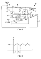
- FIG. 5 illustrates a second exemplary embodiment of the hysteretic switching regulator of the present invention.
- FIG. 6 illustrates an exemplary comparator input signal generated by the hysteretic switching regulator of FIG. 4 .
- FIG. 4 illustrates an exemplary embodiment of a hysteretic switching regulator in accordance with the present invention.
- the hysteretic switching regulator 40 includes a high-side switch 11 and a low-side switch 12 (which in the given embodiment is implemented by a diode, preferably an active diode, such as disclosed in U.S. patent application Ser. No. 11/094,369 filed on Mar. 31, 2005, which is hereby incorporated by reference in its entirety), an inductor L 15 and a capacitor C 13 which is coupled to the load 17 .
- the hysteretic switching regulator 40 further includes a low-pass filter 42 formed, for example, by resistors r 1a , r 1b and capacitor C R , which is coupled to the input of the inductor L 15 ; a buffer 43 coupled to the output of the low-pass filter 42 ; a damping/sampling circuit 44 formed, for example, by resistors r 2a , r 2b and r 3 which receives the output of the buffer 43 as an input signal, and a hysteresis comparator 16 , which receives the output of the damping/sampling circuit 44 as an input signal.
- the output of the hysteretic comparator 16 is coupled to the high-side switch 11 , and functions to control the high-side switch 11 .
- an approximately triangular control signal Vx (such as illustrated in FIG. 6 ), is generated in-part by the low-pass filter 42 , which receives and is driven by the square wave signal, Ve, at the output of the supply voltage switch 11 (i.e., the high-side switch), and is applied to the hysteretic comparator to produce the power switch drive signal 45 .
- the voltage across the capacitor C R contained in the low-pass filter 42 is approximately:
- the voltage, V X at the output of the damping/sampling circuit 44 and input to the hysteretic comparator 16 is:
- ⁇ ⁇ K 2 r 2 ⁇ ⁇ b r 2 ⁇ ⁇ a + r 2 ⁇ ⁇ b .
- V X at the input of the hysteretic comparator 16 , is triangular with average value V REF , with its positive slope defined by:
- T 1 2 ⁇ ⁇ ⁇ v ⁇ ⁇ ⁇ ( r 2 + r 3 ) ( K * V supply - V REF ) ⁇ r 2 , the negative slope period
- FIG. 6 illustrates an example of the signal, V x , present at the input of the hysteretic comparator 16 .
- the switching frequency of the hysteretic switching regulator 40 varies with V supply and V REF and is a function of fixed parameters K, ⁇ , r 2 , r 3 and ⁇ v, but, importantly, is independent of the load current.
- V OUT V REF K .
- the control signal 45 output by the comparator 16 is generated without utilizing a resistor to sense current and is nearly independent of the load current.
- the control signal 45 is generated based on the voltage signal present at the input of the inductor L 15 , which is coupled to the low-pass filter 42 , which in the given embodiment is formed by components r 1a , r 1b and C R .
- the AC component of the output of the low-pass filter 42 is a triangular ramp signal.
- the R-C time constant of the low-pass filter 42 should be sufficiently longer than the desired switching frequency period such that the substantially linear portion of the exponential response of the low-pass filter 42 is utilized to generate the ramp signal.
- resistors r 1a and r 1b of low-pass filter 42 also function to reduce the peak-to-peak voltage level of the ramp signal, thereby allowing for a reduction in the voltage swing that the buffer 43 and hysteretic comparator 16 must be able to accommodate.
- the buffer 43 functions to prevent the output of the switching regulator 40 from interacting with or loading the capacitor, C R , of the low-pass filter 42 , and generally isolates the low-pass filter 42 from the output of the switching regulator 40 . This is important, as for example, it allows for a small value capacitor to be utilized for C R .
- resistors r 2a , r 2b and r 3 form the damping circuit 44 , which functions to sample the output voltage and adjust the value of the ramp signal output by the buffer 43 prior to the ramp signal being input into the hysteresis comparator 16 .
- the values of resistor r 2a , r 2b and r 3 are selected such that the damping (or feedback) functions to control load transients, but not to affect the shape of the desired ramp control signal.
- This damping circuit 44 is especially necessary when the output of the switching regulator is coupled to a linear regulator which is essentially a current sink (as opposed to a resistive load).
- the ramp signal coupled to the input of the hysteretic comparator 16 comprises the combination of the triangular ramp signal output by the buffer and a portion of the sampled output voltage adjusted based on the values of resistor r 2a , r 2b and r 3 of the damping circuit 44 .
- the phases of voltage signal output by the buffer 43 and the sampled output signal obtained from the damping circuit 44 are substantially in quadrature with one another (as explained below, the embodiment of FIG. 5 provides for improved performance during transients).
- the ripple voltage from V OUT is at its zero value when the voltage signal from the buffer 43 is at its positive or negative peaks where the comparator 16 switches states, and the magnitude of the V OUT ripple does not affect the switching points.
- FIG. 5 illustrates a second embodiment of the present invention which allows for the output load voltage to more accurately track rapid changes in the set point (as will occur when the set point is programmable).
- the hysteretic switching regulator of the second embodiment 50 is the same as shown in FIG. 4 with the exception that the circuit 50 includes an additional buffer 52 having an input which receives V REF , and two additional components d 1 and d 2 , which are preferably active devices (similar to the active device utilized for the low-side switch as detailed above).
- the additional buffer 52 receives the V REF set point signal as an input signal, and the output of the buffer 52 is coupled to the input of buffer 43 via components d 1 and d 2 , which are coupled in parallel with one another.
- the direction (i.e., location of cathode and anode terminal) of the diodes d 1 and d 2 are opposite one another in the configuration as shown in FIG. 5 .
- components d 1 and d 2 provide the functions of diodes but are usually implemented utilizing active circuits so as to have stable forward voltage drops, which are chosen to be only slightly larger than ⁇ v*(r 2 +r 3 )/r 2 .
- the components d 1 and d 2 are off and do not affect the amplitude of the triangular voltage on C R .
- V REF changes (in either the positive or negative direction)
- one of the components d 1 and d 2 will conduct, and cause the average value of V CR to more closely follow V REF .
- the switching regulator greatly improves efficiency at small load currents. More specifically, in the prior art configurations, as shown in FIGS. 1-3 , the low-side switch 12 coupled to an input node of the inductor 15 and to ground is driven by the comparator signal with a phase opposite to that driving the high-side switch 11 . This causes the regulator to operate in “forced continuous (inductor) current” mode, in which case the direction of the inductor current, I L , is allowed to reverse when the load current is small.
- the peak-to-peak value and switching frequency of the inductor current dependant input signal to the comparator 16 are always maintained nearly constant by allowing the minimum value of inductor current to be negative when its average value (which is equal to that of the load current) is small and even zero. This allows the switching frequency to remain nearly constant as the load current becomes small, but at the cost of a drastic reduction in efficiency caused by the large value of instantaneous inductor current and switching losses in the regulator components even though the load current is small.
- the switching control signal is generated primarily by the low-pass filter 42 driven by the square wave signal at the output of the high-side switch 11 , and the amplitude of this signal is not directly related to the amplitude of the inductor current as is the case for the control signal in the prior art configurations.
- the inductor current remains zero until a decrease in output voltage, rather than low-pass filter voltage, causes the control voltage to become less than the lower threshold of the hysteresis comparator 16 , at which time the high-side switch 11 turns on again.
- the controller circuit configuration allows the switching frequency to decrease and the inductor peak current to become much smaller in magnitude (i.e., the present invention allows for operation in a discontinuous inductor current mode). This in turn reduces both switching and conduction losses, and increases efficiency.
Abstract
Description
a measure of inductor current IL can be obtained by integrating the inductor voltage:
This is typically done with an R-C low pass filter approximation to an integrator as shown in
where s is the frequency related variable in the LaPlace transform representation of a transfer function. The voltage, VX, at the output of the damping/
In normal operation of the regulator of
and its negative slope defined by:
Thus, the time for the positive slope period of the voltage at VX is
the negative slope period
and the switching frequency equals:
Usual values for the other parameters are:
and τ is chosen to give the desired switching frequency fs for typical values of Vsupply and VREF. The foregoing circuit configuration and parameter values provide for excellent response to changes in load (since there is no low pass filter between the load and the comparator input) and VOUT follows changes in set point VREF within the response time set by τ.
Claims (19)
Priority Applications (1)
| Application Number | Priority Date | Filing Date | Title |
|---|---|---|---|
| US11/633,635 US7714562B2 (en) | 2005-12-05 | 2006-12-05 | Hysteretic switching regulator |
Applications Claiming Priority (2)
| Application Number | Priority Date | Filing Date | Title |
|---|---|---|---|
| US74189605P | 2005-12-05 | 2005-12-05 | |
| US11/633,635 US7714562B2 (en) | 2005-12-05 | 2006-12-05 | Hysteretic switching regulator |
Publications (2)
| Publication Number | Publication Date |
|---|---|
| US20070145965A1 US20070145965A1 (en) | 2007-06-28 |
| US7714562B2 true US7714562B2 (en) | 2010-05-11 |
Family
ID=38243008
Family Applications (1)
| Application Number | Title | Priority Date | Filing Date |
|---|---|---|---|
| US11/633,635 Expired - Fee Related US7714562B2 (en) | 2005-12-05 | 2006-12-05 | Hysteretic switching regulator |
Country Status (2)
| Country | Link |
|---|---|
| US (1) | US7714562B2 (en) |
| JP (1) | JP4493045B2 (en) |
Cited By (16)
| Publication number | Priority date | Publication date | Assignee | Title |
|---|---|---|---|---|
| US20100283441A1 (en) * | 2009-05-08 | 2010-11-11 | Richtek Technology Corp. | Pwm controller and control method for a dc-dc voltage converter |
| US20110316501A1 (en) * | 2006-03-06 | 2011-12-29 | Enpirion, Inc. | Controller for a Power Converter and Method of Operating the Same |
| US8816662B2 (en) | 2010-05-21 | 2014-08-26 | Semiconductor Energy Laboratory Co., Ltd. | DC-DC converter, semiconductor device and display device |
| US8861145B2 (en) | 2012-07-19 | 2014-10-14 | Honeywell International Inc. | Circuit with motor driver spike suppression |
| US8922182B2 (en) | 2009-12-04 | 2014-12-30 | Semiconductor Energy Laboratory Co., Ltd. | DC converter circuit and power supply circuit |
| US20150082907A1 (en) * | 2013-09-26 | 2015-03-26 | Rosemount Inc. | Industrial process field device with low power optical isolator |
| US9083237B2 (en) | 2010-07-13 | 2015-07-14 | O2Micro, Inc. | Circuits and methods for controlling a DC/DC converter |
| US20150263715A1 (en) * | 2014-03-17 | 2015-09-17 | Samsung Electro-Mechanics Co., Ltd. | Active noise filter and gate driving device having the same |
| US9228869B2 (en) | 2013-09-26 | 2016-01-05 | Rosemount Inc. | Industrial process variable transmitter with isolated power scavenging intrinsically safe pulse output circuitry |
| US20160099640A1 (en) * | 2014-10-06 | 2016-04-07 | Samsung Electronics Co., Ltd. | Buck-boost converters and power management integrated circuits including the same |
| US20160336858A1 (en) * | 2015-05-12 | 2016-11-17 | Samsung Electronics Co., Ltd. | Power converting circuit and hysteresis buck converter |
| US9595866B2 (en) | 2013-12-24 | 2017-03-14 | Samsung Electronics Co., Ltd. | Hysteretic switching regulator including a power converting unit and a switch driving unit |
| US9793801B2 (en) | 2010-05-21 | 2017-10-17 | Semiconductor Energy Laboratory Co., Ltd. | Semiconductor device and display device |
| US10075246B2 (en) | 2013-09-26 | 2018-09-11 | Micro Motion, Inc. | Optical isolator mounted in printed circuit board recess |
| US10389224B2 (en) | 2013-12-31 | 2019-08-20 | Samsung Display Co., Ltd. | Power converter system and method of operating thereof |
| US20220158629A1 (en) * | 2020-11-19 | 2022-05-19 | Visic Technologies Ltd. | Dynamic slew rate controller |
Families Citing this family (21)
| Publication number | Priority date | Publication date | Assignee | Title |
|---|---|---|---|---|
| US7667446B2 (en) * | 2007-01-11 | 2010-02-23 | Infineon Technologies Ag | Method for controlling current in a load |
| CN100578902C (en) * | 2007-10-29 | 2010-01-06 | 华为技术有限公司 | Electric power output voltage-operated device |
| KR101045737B1 (en) * | 2007-12-12 | 2011-06-30 | 마이크렐 인코포레이티드 | Constant on-time regulator with internal ripple generation and improved output voltage accuracy |
| JP5287191B2 (en) | 2008-12-03 | 2013-09-11 | 株式会社リコー | Hysteresis switching regulator and operation control method thereof |
| JP5340721B2 (en) * | 2008-12-26 | 2013-11-13 | 富士通セミコンダクター株式会社 | Power supply |
| US8358114B1 (en) | 2009-04-28 | 2013-01-22 | Western Digital Technologies, Inc. | Output capacitor current as feedback to control a hysteretic voltage regulator |
| JP5593104B2 (en) * | 2010-03-24 | 2014-09-17 | Fdk株式会社 | Ripple converter |
| US20110267018A1 (en) * | 2010-04-30 | 2011-11-03 | Hai Tao | Ac coupled hysteretic pwm controller |
| US8487598B2 (en) * | 2010-08-30 | 2013-07-16 | Texas Instruments Incorporated | DC-DC converter with unity-gain feedback amplifier driving bias transistor |
| WO2012147609A1 (en) * | 2011-04-25 | 2012-11-01 | ローム株式会社 | Switching power source device and electronic equipment using same |
| JP5808990B2 (en) | 2011-09-13 | 2015-11-10 | リコー電子デバイス株式会社 | DC / DC converter control circuit and DC-DC converter |
| JP5812777B2 (en) | 2011-09-13 | 2015-11-17 | リコー電子デバイス株式会社 | DC / DC converter control circuit and DC-DC converter |
| JP5974563B2 (en) | 2012-03-15 | 2016-08-23 | 富士電機株式会社 | Step-up switching power supply |
| JP5728433B2 (en) * | 2012-06-11 | 2015-06-03 | 株式会社東芝 | DC-DC conversion circuit |
| CN103036432B (en) * | 2012-12-07 | 2015-02-25 | 上海电力学院 | Pulse width modulation (PWM) hysteresis control method based on ripple |
| CN103197122B (en) * | 2013-04-12 | 2015-04-08 | 矽力杰半导体技术(杭州)有限公司 | Current detection circuit and switch-type regulator provided with same |
| JP2015012694A (en) * | 2013-06-28 | 2015-01-19 | 株式会社東芝 | Power-supply circuit |
| KR102231317B1 (en) * | 2013-12-16 | 2021-03-24 | 삼성전자주식회사 | Voltage regulator and power delivering device therewith |
| JP2015139307A (en) * | 2014-01-23 | 2015-07-30 | ファナック株式会社 | Dc/dc converter |
| EP3314737B1 (en) * | 2015-06-29 | 2018-11-14 | Koninklijke Philips N.V. | Estimating an average value of an inductor current for switched-mode power converters |
| US11637490B2 (en) | 2021-06-21 | 2023-04-25 | Infineon Technologies Ag | Peak detection for current mode control in a power converter system |
Citations (47)
| Publication number | Priority date | Publication date | Assignee | Title |
|---|---|---|---|---|
| US4378530A (en) | 1979-07-04 | 1983-03-29 | Unisearch Limited | High-efficiency low-distortion amplifier |
| US4727308A (en) | 1986-08-28 | 1988-02-23 | International Business Machines Corporation | FET power converter with reduced switching loss |
| US4943902A (en) | 1987-11-23 | 1990-07-24 | Viteq Corporation | AC to DC power converter and method with integrated line current control for improving power factor |
| US4959606A (en) | 1989-01-06 | 1990-09-25 | Uniphase Corporation | Current mode switching regulator with programmed offtime |
| US5305192A (en) | 1991-11-01 | 1994-04-19 | Linear Technology Corporation | Switching regulator circuit using magnetic flux-sensing |
| US5420532A (en) | 1993-08-20 | 1995-05-30 | Texas Instruments Incorporated | Synchronous rectifying circuit |
| US5420530A (en) | 1986-09-18 | 1995-05-30 | Canon Kabushiki Kaisha | Voltage comparator with hysteresis |
| US5479090A (en) | 1993-11-24 | 1995-12-26 | Raytheon Company | Power converter having optimal dynamic operation |
| US5600234A (en) | 1995-03-01 | 1997-02-04 | Texas Instruments Incorporated | Switch mode power converter and method |
| US5903447A (en) | 1997-07-23 | 1999-05-11 | Murata Manufacturing Co., Ltd. | Current-mode control device and switching power supply employing same |
| US5905407A (en) | 1997-07-30 | 1999-05-18 | Motorola, Inc. | High efficiency power amplifier using combined linear and switching techniques with novel feedback system |
| US5929620A (en) | 1996-11-07 | 1999-07-27 | Linear Technology Corporation | Switching regulators having a synchronizable oscillator frequency with constant ramp amplitude |
| US5949229A (en) | 1996-08-28 | 1999-09-07 | Samsung Electronics, Co., Ltd. | Power factor correction circuit having an error signal multiplied by a current signal |
| US5982160A (en) | 1998-12-24 | 1999-11-09 | Harris Corporation | DC-to-DC converter with inductor current sensing and related methods |
| US5991182A (en) | 1995-12-29 | 1999-11-23 | Em Microelectric -Marin Sa | Active rectifier having minimal energy losses |
| US6034517A (en) | 1998-10-27 | 2000-03-07 | Linear Technology Corporation | High efficiency step-down switching regulators |
| US6046516A (en) | 1994-10-28 | 2000-04-04 | Siemens Aktiengesellschaft | Electronic switch for use with inductive loads |
| US6066943A (en) | 1998-10-08 | 2000-05-23 | Texas Instruments Incorporated | Capacitive-summing switch-mode power conversion control |
| US6147478A (en) | 1999-09-17 | 2000-11-14 | Texas Instruments Incorporated | Hysteretic regulator and control method having switching frequency independent from output filter |
| US6166528A (en) | 1999-11-02 | 2000-12-26 | Fairchild Semiconductor Corporation | Lossless current sensing in buck converters working with low duty cycles and high clock frequencies |
| US6222356B1 (en) | 1998-04-01 | 2001-04-24 | Siemens Aktiengesellschaft | Current mode switching regulator configured such that a measuring resistor is not needed to measure the current at an inductor |
| US6268756B1 (en) | 1999-03-31 | 2001-07-31 | Sony Corporation | Fast high side switch for hard disk drive preamplifiers |
| US6304066B1 (en) | 1993-03-23 | 2001-10-16 | Linear Technology Corporation | Control circuit and method for maintaining high efficiency over broad current ranges in a switching regular circuit |
| US6307356B1 (en) | 1998-06-18 | 2001-10-23 | Linear Technology Corporation | Voltage mode feedback burst mode circuit |
| US6313610B1 (en) | 1999-08-20 | 2001-11-06 | Texas Instruments Incorporated | Battery protection circuit employing active regulation of charge and discharge devices |
| US6366070B1 (en) | 2001-07-12 | 2002-04-02 | Analog Devices, Inc. | Switching voltage regulator with dual modulation control scheme |
| US6396250B1 (en) | 2000-08-31 | 2002-05-28 | Texas Instruments Incorporated | Control method to reduce body diode conduction and reverse recovery losses |
| US6404261B1 (en) | 1999-03-27 | 2002-06-11 | Koninklijke Philips Electronics N.V. | Switch circuit and semiconductor switch, for battery-powered equipment |
| US6476589B2 (en) | 2001-04-06 | 2002-11-05 | Linear Technology Corporation | Circuits and methods for synchronizing non-constant frequency switching regulators with a phase locked loop |
| US6498466B1 (en) | 2000-05-23 | 2002-12-24 | Linear Technology Corp. | Cancellation of slope compensation effect on current limit |
| US6509721B1 (en) | 2001-08-27 | 2003-01-21 | Koninklijke Philips Electronics N.V. | Buck regulator with ability to handle rapid reduction of load current |
| US6522178B2 (en) | 1999-04-22 | 2003-02-18 | International Rectifier Corporation | Controlling high side devices without using level shift switches |
| US6541947B1 (en) | 1998-09-10 | 2003-04-01 | Robert Bosch Gmbh | Step-down constant-current transformer |
| US6563725B2 (en) * | 2001-10-03 | 2003-05-13 | Bruce W. Carsten | Apparatus and method for control and driving BJT used as synchronous rectifier |
| WO2003047080A1 (en) | 2001-11-29 | 2003-06-05 | Sanken Electric Co., Ltd. | Switching power supply |
| US6583610B2 (en) * | 2001-03-12 | 2003-06-24 | Semtech Corporation | Virtual ripple generation in switch-mode power supplies |
| US6724174B1 (en) | 2002-09-12 | 2004-04-20 | Linear Technology Corp. | Adjustable minimum peak inductor current level for burst mode in current-mode DC-DC regulators |
| US6744241B2 (en) | 2002-06-07 | 2004-06-01 | Infineon Technologies Ag | Method for driving a switch in a switch-mode converter, and a drive circuit for driving a switch |
| US6828766B2 (en) | 2002-05-30 | 2004-12-07 | Stmicroelectronics S.R.L. | Voltage regulator |
| US6873140B2 (en) | 2002-07-12 | 2005-03-29 | Stmicroelectronics S.R.L. | Digital contoller for DC-DC switching converters |
| US6894471B2 (en) | 2002-05-31 | 2005-05-17 | St Microelectronics S.R.L. | Method of regulating the supply voltage of a load and related voltage regulator |
| US6958594B2 (en) * | 2004-01-21 | 2005-10-25 | Analog Devices, Inc. | Switched noise filter circuit for a DC-DC converter |
| US6979985B2 (en) | 2002-06-07 | 2005-12-27 | Renesas Technology Corp. | Switching power supply device and switching power supply system |
| US6984966B2 (en) * | 2003-09-05 | 2006-01-10 | Shindengen Electric Manufacturing Co., Ltd. | Switching power supply |
| US7019504B2 (en) * | 2003-07-08 | 2006-03-28 | Arques Technology | Constant ON-time controller for a buck converter |
| US7030596B1 (en) | 2003-12-03 | 2006-04-18 | Linear Technology Corporation | Methods and circuits for programmable automatic burst mode control using average output current |
| US20070018617A1 (en) | 2005-07-19 | 2007-01-25 | Mitsumi Electric Co., Ltd. | Current resonance type DC/DC converter capable of decreasing losses on on-load and a light load |
Family Cites Families (2)
| Publication number | Priority date | Publication date | Assignee | Title |
|---|---|---|---|---|
| US6037517A (en) * | 1998-11-04 | 2000-03-14 | Clean Technologies International Corporation | Apparatus and method for treating waste materials which include charged particle emitters |
| US7422736B2 (en) * | 2002-07-26 | 2008-09-09 | Food Industry Research And Development Institute | Somatic pluripotent cells |
-
2006
- 2006-12-05 JP JP2006327822A patent/JP4493045B2/en active Active
- 2006-12-05 US US11/633,635 patent/US7714562B2/en not_active Expired - Fee Related
Patent Citations (52)
| Publication number | Priority date | Publication date | Assignee | Title |
|---|---|---|---|---|
| US4378530A (en) | 1979-07-04 | 1983-03-29 | Unisearch Limited | High-efficiency low-distortion amplifier |
| US4727308A (en) | 1986-08-28 | 1988-02-23 | International Business Machines Corporation | FET power converter with reduced switching loss |
| US5420530A (en) | 1986-09-18 | 1995-05-30 | Canon Kabushiki Kaisha | Voltage comparator with hysteresis |
| US4943902A (en) | 1987-11-23 | 1990-07-24 | Viteq Corporation | AC to DC power converter and method with integrated line current control for improving power factor |
| US4959606A (en) | 1989-01-06 | 1990-09-25 | Uniphase Corporation | Current mode switching regulator with programmed offtime |
| US5305192A (en) | 1991-11-01 | 1994-04-19 | Linear Technology Corporation | Switching regulator circuit using magnetic flux-sensing |
| US6304066B1 (en) | 1993-03-23 | 2001-10-16 | Linear Technology Corporation | Control circuit and method for maintaining high efficiency over broad current ranges in a switching regular circuit |
| US5420532A (en) | 1993-08-20 | 1995-05-30 | Texas Instruments Incorporated | Synchronous rectifying circuit |
| US5479090A (en) | 1993-11-24 | 1995-12-26 | Raytheon Company | Power converter having optimal dynamic operation |
| US6046516A (en) | 1994-10-28 | 2000-04-04 | Siemens Aktiengesellschaft | Electronic switch for use with inductive loads |
| US5600234A (en) | 1995-03-01 | 1997-02-04 | Texas Instruments Incorporated | Switch mode power converter and method |
| US5991182A (en) | 1995-12-29 | 1999-11-23 | Em Microelectric -Marin Sa | Active rectifier having minimal energy losses |
| US5949229A (en) | 1996-08-28 | 1999-09-07 | Samsung Electronics, Co., Ltd. | Power factor correction circuit having an error signal multiplied by a current signal |
| US5929620A (en) | 1996-11-07 | 1999-07-27 | Linear Technology Corporation | Switching regulators having a synchronizable oscillator frequency with constant ramp amplitude |
| US5903447A (en) | 1997-07-23 | 1999-05-11 | Murata Manufacturing Co., Ltd. | Current-mode control device and switching power supply employing same |
| US5905407A (en) | 1997-07-30 | 1999-05-18 | Motorola, Inc. | High efficiency power amplifier using combined linear and switching techniques with novel feedback system |
| US6222356B1 (en) | 1998-04-01 | 2001-04-24 | Siemens Aktiengesellschaft | Current mode switching regulator configured such that a measuring resistor is not needed to measure the current at an inductor |
| US6307356B1 (en) | 1998-06-18 | 2001-10-23 | Linear Technology Corporation | Voltage mode feedback burst mode circuit |
| US6541947B1 (en) | 1998-09-10 | 2003-04-01 | Robert Bosch Gmbh | Step-down constant-current transformer |
| US6066943A (en) | 1998-10-08 | 2000-05-23 | Texas Instruments Incorporated | Capacitive-summing switch-mode power conversion control |
| US6034517A (en) | 1998-10-27 | 2000-03-07 | Linear Technology Corporation | High efficiency step-down switching regulators |
| US5982160A (en) | 1998-12-24 | 1999-11-09 | Harris Corporation | DC-to-DC converter with inductor current sensing and related methods |
| US6404261B1 (en) | 1999-03-27 | 2002-06-11 | Koninklijke Philips Electronics N.V. | Switch circuit and semiconductor switch, for battery-powered equipment |
| US6268756B1 (en) | 1999-03-31 | 2001-07-31 | Sony Corporation | Fast high side switch for hard disk drive preamplifiers |
| US6522178B2 (en) | 1999-04-22 | 2003-02-18 | International Rectifier Corporation | Controlling high side devices without using level shift switches |
| US6313610B1 (en) | 1999-08-20 | 2001-11-06 | Texas Instruments Incorporated | Battery protection circuit employing active regulation of charge and discharge devices |
| US6147478A (en) | 1999-09-17 | 2000-11-14 | Texas Instruments Incorporated | Hysteretic regulator and control method having switching frequency independent from output filter |
| US6166528A (en) | 1999-11-02 | 2000-12-26 | Fairchild Semiconductor Corporation | Lossless current sensing in buck converters working with low duty cycles and high clock frequencies |
| US20030025484A1 (en) | 2000-05-23 | 2003-02-06 | Linear Technology Corporation | Cancellation of slope compensation effect on current limit |
| US6611131B2 (en) | 2000-05-23 | 2003-08-26 | Linear Technology Corp. | Cancellation of slope compensation effect on current limit |
| US6498466B1 (en) | 2000-05-23 | 2002-12-24 | Linear Technology Corp. | Cancellation of slope compensation effect on current limit |
| US6396250B1 (en) | 2000-08-31 | 2002-05-28 | Texas Instruments Incorporated | Control method to reduce body diode conduction and reverse recovery losses |
| US6583610B2 (en) * | 2001-03-12 | 2003-06-24 | Semtech Corporation | Virtual ripple generation in switch-mode power supplies |
| US6476589B2 (en) | 2001-04-06 | 2002-11-05 | Linear Technology Corporation | Circuits and methods for synchronizing non-constant frequency switching regulators with a phase locked loop |
| US6366070B1 (en) | 2001-07-12 | 2002-04-02 | Analog Devices, Inc. | Switching voltage regulator with dual modulation control scheme |
| US6509721B1 (en) | 2001-08-27 | 2003-01-21 | Koninklijke Philips Electronics N.V. | Buck regulator with ability to handle rapid reduction of load current |
| US6563725B2 (en) * | 2001-10-03 | 2003-05-13 | Bruce W. Carsten | Apparatus and method for control and driving BJT used as synchronous rectifier |
| US20050018458A1 (en) | 2001-11-29 | 2005-01-27 | Masaaki Shimada | Switching power supply device |
| WO2003047080A1 (en) | 2001-11-29 | 2003-06-05 | Sanken Electric Co., Ltd. | Switching power supply |
| US6828766B2 (en) | 2002-05-30 | 2004-12-07 | Stmicroelectronics S.R.L. | Voltage regulator |
| US6894471B2 (en) | 2002-05-31 | 2005-05-17 | St Microelectronics S.R.L. | Method of regulating the supply voltage of a load and related voltage regulator |
| US7109693B2 (en) | 2002-06-07 | 2006-09-19 | Renesas Technology Corp. | Switching power supply device and switching power supply system |
| US6744241B2 (en) | 2002-06-07 | 2004-06-01 | Infineon Technologies Ag | Method for driving a switch in a switch-mode converter, and a drive circuit for driving a switch |
| US6979985B2 (en) | 2002-06-07 | 2005-12-27 | Renesas Technology Corp. | Switching power supply device and switching power supply system |
| US7091711B2 (en) | 2002-06-07 | 2006-08-15 | Renesas Technology Corp. | Switching power supply device and switching power supply system |
| US6873140B2 (en) | 2002-07-12 | 2005-03-29 | Stmicroelectronics S.R.L. | Digital contoller for DC-DC switching converters |
| US6724174B1 (en) | 2002-09-12 | 2004-04-20 | Linear Technology Corp. | Adjustable minimum peak inductor current level for burst mode in current-mode DC-DC regulators |
| US7019504B2 (en) * | 2003-07-08 | 2006-03-28 | Arques Technology | Constant ON-time controller for a buck converter |
| US6984966B2 (en) * | 2003-09-05 | 2006-01-10 | Shindengen Electric Manufacturing Co., Ltd. | Switching power supply |
| US7030596B1 (en) | 2003-12-03 | 2006-04-18 | Linear Technology Corporation | Methods and circuits for programmable automatic burst mode control using average output current |
| US6958594B2 (en) * | 2004-01-21 | 2005-10-25 | Analog Devices, Inc. | Switched noise filter circuit for a DC-DC converter |
| US20070018617A1 (en) | 2005-07-19 | 2007-01-25 | Mitsumi Electric Co., Ltd. | Current resonance type DC/DC converter capable of decreasing losses on on-load and a light load |
Non-Patent Citations (4)
| Title |
|---|
| Castilla, M., Garcia de Vicuña, L., Guerrero, J. M., Matas, J., & Miret, J. (2005). Design of voltage-mode hysteretic controllers for synchronous buck converters supplying microprocessor loads. IEE Proceedings-Electric Power Applications, 152(5), 1171-1178. doi: 10.1049/ip-epa:20045276. * |
| Castilla, M., Garcia de Vicuña, L., Guerrero, J. M., Matas, J., & Miret, J. (2005). Design of voltage-mode hysteretic controllers for synchronous buck converters supplying microprocessor loads. IEE Proceedings—Electric Power Applications, 152(5), 1171-1178. doi: 10.1049/ip-epa:20045276. * |
| Japanese Notice of Reasons for Rejections, w/ English translation thereof, issued in Japanese Patent Application No. JP 2006-327822 dated Nov. 10, 2009. |
| Philip T. Krein, "Geometric Control for Power Converters," Elements of Power Electronics, Oxford University Press, 1998, pp. 662-676. |
Cited By (24)
| Publication number | Priority date | Publication date | Assignee | Title |
|---|---|---|---|---|
| US20110316501A1 (en) * | 2006-03-06 | 2011-12-29 | Enpirion, Inc. | Controller for a Power Converter and Method of Operating the Same |
| US8736241B2 (en) * | 2006-03-06 | 2014-05-27 | Enpirion, Inc. | Controller for a power converter and method of operating the same |
| US20100283441A1 (en) * | 2009-05-08 | 2010-11-11 | Richtek Technology Corp. | Pwm controller and control method for a dc-dc voltage converter |
| US8525505B2 (en) * | 2009-05-08 | 2013-09-03 | Richtek Technology Corp. | PWM controller and control method for a DC-DC voltage converter |
| US9270173B2 (en) | 2009-12-04 | 2016-02-23 | Semiconductor Energy Laboratory Co., Ltd. | DC converter circuit and power supply circuit |
| US8922182B2 (en) | 2009-12-04 | 2014-12-30 | Semiconductor Energy Laboratory Co., Ltd. | DC converter circuit and power supply circuit |
| US9793801B2 (en) | 2010-05-21 | 2017-10-17 | Semiconductor Energy Laboratory Co., Ltd. | Semiconductor device and display device |
| US8816662B2 (en) | 2010-05-21 | 2014-08-26 | Semiconductor Energy Laboratory Co., Ltd. | DC-DC converter, semiconductor device and display device |
| US9083237B2 (en) | 2010-07-13 | 2015-07-14 | O2Micro, Inc. | Circuits and methods for controlling a DC/DC converter |
| US8861145B2 (en) | 2012-07-19 | 2014-10-14 | Honeywell International Inc. | Circuit with motor driver spike suppression |
| US9228869B2 (en) | 2013-09-26 | 2016-01-05 | Rosemount Inc. | Industrial process variable transmitter with isolated power scavenging intrinsically safe pulse output circuitry |
| US9175993B2 (en) * | 2013-09-26 | 2015-11-03 | Rosemount Inc. | Industrial process field device with low power optical isolator |
| US20150082907A1 (en) * | 2013-09-26 | 2015-03-26 | Rosemount Inc. | Industrial process field device with low power optical isolator |
| US10075246B2 (en) | 2013-09-26 | 2018-09-11 | Micro Motion, Inc. | Optical isolator mounted in printed circuit board recess |
| US9595866B2 (en) | 2013-12-24 | 2017-03-14 | Samsung Electronics Co., Ltd. | Hysteretic switching regulator including a power converting unit and a switch driving unit |
| US10389224B2 (en) | 2013-12-31 | 2019-08-20 | Samsung Display Co., Ltd. | Power converter system and method of operating thereof |
| US20150263715A1 (en) * | 2014-03-17 | 2015-09-17 | Samsung Electro-Mechanics Co., Ltd. | Active noise filter and gate driving device having the same |
| KR101942726B1 (en) | 2014-03-17 | 2019-01-28 | 삼성전기 주식회사 | Active noise filter and gate driving device having the same |
| US20160099640A1 (en) * | 2014-10-06 | 2016-04-07 | Samsung Electronics Co., Ltd. | Buck-boost converters and power management integrated circuits including the same |
| US9705401B2 (en) * | 2014-10-06 | 2017-07-11 | Samsung Electronics Co., Ltd. | Buck-boost converters and power management integrated circuits including the same |
| US9768695B2 (en) * | 2015-05-12 | 2017-09-19 | Samsung Electronics Co., Ltd. | Power converting circuit and hysteresis buck converter with changing response characteristic based on transient state of output voltage |
| US20160336858A1 (en) * | 2015-05-12 | 2016-11-17 | Samsung Electronics Co., Ltd. | Power converting circuit and hysteresis buck converter |
| US20220158629A1 (en) * | 2020-11-19 | 2022-05-19 | Visic Technologies Ltd. | Dynamic slew rate controller |
| US11764768B2 (en) * | 2020-11-19 | 2023-09-19 | Visic Technologies Ltd. | Dynamic slew rate controller |
Also Published As
| Publication number | Publication date |
|---|---|
| US20070145965A1 (en) | 2007-06-28 |
| JP4493045B2 (en) | 2010-06-30 |
| JP2007159395A (en) | 2007-06-21 |
Similar Documents
| Publication | Publication Date | Title |
|---|---|---|
| US7714562B2 (en) | Hysteretic switching regulator | |
| US6348780B1 (en) | Frequency control of hysteretic power converter by adjusting hystersis levels | |
| US6222356B1 (en) | Current mode switching regulator configured such that a measuring resistor is not needed to measure the current at an inductor | |
| US6150739A (en) | Circuit configuration for supplying power to electronic tripping device | |
| EP1309077B1 (en) | Method and apparatus for sensing output inductor current in a dc-to-dc power converter | |
| JP4405438B2 (en) | Slope compensation switching regulator and compensation method thereof | |
| US6642696B2 (en) | DC-DC converter with a feedback controller | |
| US6377032B1 (en) | Method and apparatus for virtual current sensing in DC-DC switched mode power supplies | |
| US7714547B2 (en) | Method and apparatus for constant on-time switch mode converters | |
| US4881023A (en) | Hybrid high speed voltage regulator with reduction of miller effect | |
| US7254000B1 (en) | Over voltage protection scheme for synchronous buck converter | |
| US5982160A (en) | DC-to-DC converter with inductor current sensing and related methods | |
| US6807070B2 (en) | Resonant converter with phase delay control | |
| EP1367703A1 (en) | Method of regulation of the supply voltage of a load and relative voltage regulator | |
| US6160388A (en) | Sensing of current in a synchronous-buck power stage | |
| US6909268B2 (en) | Current-mode switching regulator | |
| US10193449B2 (en) | Buck voltage converter | |
| JP2002281742A (en) | Current mode dc-dc converter | |
| JP2022062700A (en) | Dynamic bias technique for enhanced mosfet on-resistance based current sensing | |
| US6809560B1 (en) | Load sensing circuit for a power MOSFET switch | |
| JP2004343997A (en) | Active voltage positioning method and implementation | |
| JP3566201B2 (en) | Chopper type regulator | |
| US7208926B2 (en) | Switching signal modulation circuit | |
| JPH03215168A (en) | Multioutput converter and modulating circuit thereof | |
| EP1087506A2 (en) | Frequency control of switch-mode power supply |
Legal Events
| Date | Code | Title | Description |
|---|---|---|---|
| AS | Assignment |
Owner name: MATSUSHITA ELECTRIC INDUSTRIAL CO., LTD.,JAPAN Free format text: ASSIGNMENT OF ASSIGNORS INTEREST;ASSIGNORS:OSWALD, RICHARD;YAMAMOTO, TAMOTSU;RYU, TAKASHI;AND OTHERS;SIGNING DATES FROM 20070213 TO 20070216;REEL/FRAME:018980/0251 Owner name: MATSUSHITA ELECTRIC INDUSTRIAL CO., LTD., JAPAN Free format text: ASSIGNMENT OF ASSIGNORS INTEREST;ASSIGNORS:OSWALD, RICHARD;YAMAMOTO, TAMOTSU;RYU, TAKASHI;AND OTHERS;REEL/FRAME:018980/0251;SIGNING DATES FROM 20070213 TO 20070216 |
|
| AS | Assignment |
Owner name: PANASONIC CORPORATION, JAPAN Free format text: CHANGE OF NAME;ASSIGNOR:MATSUSHITA ELECTRIC INDUSTRIAL CO., LTD.;REEL/FRAME:021897/0707 Effective date: 20081001 Owner name: PANASONIC CORPORATION,JAPAN Free format text: CHANGE OF NAME;ASSIGNOR:MATSUSHITA ELECTRIC INDUSTRIAL CO., LTD.;REEL/FRAME:021897/0707 Effective date: 20081001 |
|
| FEPP | Fee payment procedure |
Free format text: PAYOR NUMBER ASSIGNED (ORIGINAL EVENT CODE: ASPN); ENTITY STATUS OF PATENT OWNER: LARGE ENTITY |
|
| STCF | Information on status: patent grant |
Free format text: PATENTED CASE |
|
| FPAY | Fee payment |
Year of fee payment: 4 |
|
| MAFP | Maintenance fee payment |
Free format text: PAYMENT OF MAINTENANCE FEE, 8TH YEAR, LARGE ENTITY (ORIGINAL EVENT CODE: M1552) Year of fee payment: 8 |
|
| AS | Assignment |
Owner name: PANASONIC SEMICONDUCTOR SOLUTIONS CO., LTD., JAPAN Free format text: ASSIGNMENT OF ASSIGNORS INTEREST;ASSIGNOR:PANASONIC CORPORATION;REEL/FRAME:052755/0917 Effective date: 20200521 |
|
| LAPS | Lapse for failure to pay maintenance fees |
Free format text: PATENT EXPIRED FOR FAILURE TO PAY MAINTENANCE FEES (ORIGINAL EVENT CODE: EXP.); ENTITY STATUS OF PATENT OWNER: LARGE ENTITY |
|
| FEPP | Fee payment procedure |
Free format text: MAINTENANCE FEE REMINDER MAILED (ORIGINAL EVENT CODE: REM.); ENTITY STATUS OF PATENT OWNER: LARGE ENTITY |
|
| STCH | Information on status: patent discontinuation |
Free format text: PATENT EXPIRED DUE TO NONPAYMENT OF MAINTENANCE FEES UNDER 37 CFR 1.362 |
|
| FP | Lapsed due to failure to pay maintenance fee |
Effective date: 20220511 |