US7714554B2 - Forward power converter controllers - Google Patents
Forward power converter controllers Download PDFInfo
- Publication number
- US7714554B2 US7714554B2 US11/732,107 US73210707A US7714554B2 US 7714554 B2 US7714554 B2 US 7714554B2 US 73210707 A US73210707 A US 73210707A US 7714554 B2 US7714554 B2 US 7714554B2
- Authority
- US
- United States
- Prior art keywords
- transformer
- converter
- resonant
- switch
- period
- Prior art date
- Legal status (The legal status is an assumption and is not a legal conclusion. Google has not performed a legal analysis and makes no representation as to the accuracy of the status listed.)
- Expired - Fee Related, expires
Links
Images


Classifications
-
- H—ELECTRICITY
- H02—GENERATION; CONVERSION OR DISTRIBUTION OF ELECTRIC POWER
- H02M—APPARATUS FOR CONVERSION BETWEEN AC AND AC, BETWEEN AC AND DC, OR BETWEEN DC AND DC, AND FOR USE WITH MAINS OR SIMILAR POWER SUPPLY SYSTEMS; CONVERSION OF DC OR AC INPUT POWER INTO SURGE OUTPUT POWER; CONTROL OR REGULATION THEREOF
- H02M1/00—Details of apparatus for conversion
- H02M1/14—Arrangements for reducing ripples from dc input or output
-
- H—ELECTRICITY
- H02—GENERATION; CONVERSION OR DISTRIBUTION OF ELECTRIC POWER
- H02M—APPARATUS FOR CONVERSION BETWEEN AC AND AC, BETWEEN AC AND DC, OR BETWEEN DC AND DC, AND FOR USE WITH MAINS OR SIMILAR POWER SUPPLY SYSTEMS; CONVERSION OF DC OR AC INPUT POWER INTO SURGE OUTPUT POWER; CONTROL OR REGULATION THEREOF
- H02M3/00—Conversion of dc power input into dc power output
- H02M3/22—Conversion of dc power input into dc power output with intermediate conversion into ac
- H02M3/24—Conversion of dc power input into dc power output with intermediate conversion into ac by static converters
- H02M3/28—Conversion of dc power input into dc power output with intermediate conversion into ac by static converters using discharge tubes with control electrode or semiconductor devices with control electrode to produce the intermediate ac
- H02M3/325—Conversion of dc power input into dc power output with intermediate conversion into ac by static converters using discharge tubes with control electrode or semiconductor devices with control electrode to produce the intermediate ac using devices of a triode or a transistor type requiring continuous application of a control signal
- H02M3/335—Conversion of dc power input into dc power output with intermediate conversion into ac by static converters using discharge tubes with control electrode or semiconductor devices with control electrode to produce the intermediate ac using devices of a triode or a transistor type requiring continuous application of a control signal using semiconductor devices only
- H02M3/33538—Conversion of dc power input into dc power output with intermediate conversion into ac by static converters using discharge tubes with control electrode or semiconductor devices with control electrode to produce the intermediate ac using devices of a triode or a transistor type requiring continuous application of a control signal using semiconductor devices only of the forward type
-
- H—ELECTRICITY
- H02—GENERATION; CONVERSION OR DISTRIBUTION OF ELECTRIC POWER
- H02M—APPARATUS FOR CONVERSION BETWEEN AC AND AC, BETWEEN AC AND DC, OR BETWEEN DC AND DC, AND FOR USE WITH MAINS OR SIMILAR POWER SUPPLY SYSTEMS; CONVERSION OF DC OR AC INPUT POWER INTO SURGE OUTPUT POWER; CONTROL OR REGULATION THEREOF
- H02M1/00—Details of apparatus for conversion
- H02M1/0048—Circuits or arrangements for reducing losses
- H02M1/0054—Transistor switching losses
- H02M1/0058—Transistor switching losses by employing soft switching techniques, i.e. commutation of transistors when applied voltage is zero or when current flow is zero
-
- Y—GENERAL TAGGING OF NEW TECHNOLOGICAL DEVELOPMENTS; GENERAL TAGGING OF CROSS-SECTIONAL TECHNOLOGIES SPANNING OVER SEVERAL SECTIONS OF THE IPC; TECHNICAL SUBJECTS COVERED BY FORMER USPC CROSS-REFERENCE ART COLLECTIONS [XRACs] AND DIGESTS
- Y02—TECHNOLOGIES OR APPLICATIONS FOR MITIGATION OR ADAPTATION AGAINST CLIMATE CHANGE
- Y02B—CLIMATE CHANGE MITIGATION TECHNOLOGIES RELATED TO BUILDINGS, e.g. HOUSING, HOUSE APPLIANCES OR RELATED END-USER APPLICATIONS
- Y02B70/00—Technologies for an efficient end-user side electric power management and consumption
- Y02B70/10—Technologies improving the efficiency by using switched-mode power supplies [SMPS], i.e. efficient power electronics conversion e.g. power factor correction or reduction of losses in power supplies or efficient standby modes
Definitions
- This invention relates to control techniques and controllers for resonant discontinuous forward power converters (RDFCs).
- RDFCs discontinuous forward power converters
- FIG. 1 (which is taken from U.S. Pat. No. 4,688,160) shows an example of a forward power converter comprising a dc input 101 , 102 coupled to the primary winding 109 of a transformer 110 .
- the primary winding 109 is connected in series with a switching device 105 , here a bipolar transistor, which switches on and off, during an on period building up magnetising flux in the primary winding 109 , which drives a current in a secondary winding 111 of the transformer.
- a switching device 105 here a bipolar transistor, which switches on and off, during an on period building up magnetising flux in the primary winding 109 , which drives a current in a secondary winding 111 of the transformer.
- the primary and secondary windings have matched polarities, as indicated by the dots on the windings in FIG. 1 .
- the output from the transformer 110 is rectified by a rectifier 114 and smoothed by a smoothing capacitor 119 to provide a do output 121 , 122 .
- switch 105 When switch 105 is off the core of the transformer is “reset” allowing the magnetising flux to return to its initial state. In the example of FIG. 1 (U.S. Pat. No. 4,688,160) this is performed by resonant action between the magnetising inductance of transformer 110 and a capacitor 113 shunting diode 114 , returning energy to the input voltage source.
- the circuit of FIG. 1 includes a large output choke 117 between rectifier 114 and smoothing capacitor 119 , and a freewheeling or “flyback” diode 115 across the series combination of choke 117 and smoothing capacitor 119 . This is because when the switch 105 is turned off, because the primary and secondary windings have the same sense, rectifier 114 immediately becomes non-conducting.
- the function of the freewheeling diode 115 is to allow the choke 117 to maintain a continuous output current into output node “X” when switch 105 is off by providing a path for this current.
- FIG. 1 shows a conventional, continuous forward converter.
- FIG. 1 shows a conventional, continuous forward converter.
- FIG. 1 shows a conventional, continuous forward converter.
- U.S. Pat. No. 4,415,959 U.S. Pat. No. 6,760,236
- U.S. Pat. No. 6,304,463 U.S. Pat. No. 6,252,781
- EP0 074 399 EP0 074 399
- the reference design SLUA276 for the Texas Instruments UCC38C42 In some of these later circuits the secondary side diodes are replaced by synchronous rectifiers embodied in MOS transistors.
- Other background prior art can be found in U.S. Pat. No.
- the present invention provides a method of controlling a resonant discontinuous forward converter (RDFC), said converter including a transformer with primary and secondary matched polarity windings and a switch to, in operation, cyclically switch DC power to said primary winding of said transformer, said converter further having a DC output coupled to said secondary winding of said converter, said method comprising: sensing a transformer signal, said transformer signal representing a voltage across a winding of said transformer or a resonant current in a winding of said transformer; calculating a resonance period of said RDFC from said sensed transformer signal; and controlling an off duration of said switch in response to said calculated resonance period such that a sub-harmonic oscillation in said resonant voltage across said primary winding is reduced.
- RDFC discontinuous forward converter
- calculating a resonance period of said RDFC comprises: setting a resonance period value; measuring an initial resonance period value using one or more previous converter cycles, each of said converter cycles representing a complete on and off period of said switch; and updating said resonance period value in response to said measurement.
- said updating comprises increasing said resonance period value in response to a resonant period in said one or more previous converter cycles that is greater than said resonant period value, and decreased in response to a resonant period in said one or more previous converter cycles that is less than said resonant period value.
- said period is calculated using said sensed transformer signal from a first number of converter cycles following startup of said RDFC.
- said first number of cycles is less than 50.
- said first number of cycles is the first cycle following startup.
- said calculated resonance period is offset by an amount from one converter cycle to the next converter cycle.
- said off duration of said switch is further controlled in response to a value of said sensed transformer signal, said off duration of said switch being increased in response to an increasing sensed transformer signal.
- the present invention also provides a method of reducing sub-harmonic oscillations in a resonant voltage across a primary winding of a resonant discontinuous forward converter (RDFC), said converter including a transformer with primary and secondary matched polarity windings and a switch to, in operation, cyclically switch DC power to said primary winding of said transformer, said converter further having a DC output coupled to said secondary winding of said converter, said method comprising: sensing a transformer signal, said transformer signal representing a voltage across a winding of said transformer or a resonant current in a winding of said transformer; calculating a resonance period of said RDFC from said sensed transformer signal; and controlling an off duration of said switch in response to said calculated resonance period such that sub-harmonic oscillations in said resonant voltage across said primary windings are reduced.
- RDFC discontinuous forward converter
- calculating a resonance period of said RDFC comprises: setting a resonance period value; measuring an said initial resonance period value using one or more previous converter cycles, each of said converter cycles representing a complete on and off period of said switch; and updating said resonance period value in response to said measurement.
- said updating comprises increasing said resonance period value in response to a resonant period in said one or more previous converter cycles that is greater than said resonant period value, and decreased in response to a resonant period in said one or more previous converter cycles that is less than said resonant period value.
- said period is calculated using said sensed transformer signal from a first number of converter cycles.
- said first number of cycles is less than 50.
- said first number of cycles is the first cycle following startup.
- said calculated resonance period is offset by an amount from one converter cycle to the next converter cycle.
- said off duration of said switch is further controlled in response to a value of said sensed transformer signal, said off duration of said switch being increased in response to an increasing sensed transformer signal.
- the present invention further provides a controller for controlling a resonant discontinuous forward converter (RDFC), said converter including a transformer with primary and secondary matched polarity windings and a switch to, in operation, cyclically switch DC power to said primary winding of said transformer, said converter further having a DC output coupled to said secondary winding of said converter, comprising: an input to sense a transformer signal, said transformer signal representing a voltage across a winding of said transformer or a resonant current in a winding of said transformer; a system to calculate a resonance period of said RDFC from said sensed transformer signal; and an output to control an off duration of said switch in response to said calculated resonance period such that a sub-harmonic oscillation in said resonant voltage across said primary winding is reduced.
- RDFC discontinuous forward converter
- the present invention also provides a controller configured to reduce sub-harmonic oscillations in a resonant voltage across a primary winding of a resonant discontinuous forward converter (RDFC), said converter including a transformer with primary and secondary matched polarity windings and a switch to, in operation, cyclically switch DC power to said primary winding of said transformer, said converter further having a DC output coupled to said secondary winding of said converter, the controller comprising: means for sensing a transformer signal, said transformer signal representing a resonant voltage across a winding of said transformer or a resonant current in a winding of said transformer; means for calculating a resonance period of said RDFC from said sensed transformer signal; and means for controlling an off duration of said switch in response to said calculated resonance period such that sub-harmonic oscillations in said resonant voltage across said primary windings are reduced.
- RDFC discontinuous forward converter
- the present invention also provides a resonant discontinuous forward converter (RDFC) including a controller according to the above statements.
- RDFC resonant discontinuous forward converter
- FIG. 1 shows an example of a forward converter according to the prior art
- FIG. 2 shows a basic circuit diagram of an RDFC
- FIGS. 3 a , 3 b , 3 c , 3 d and 3 e show example waveforms of converter operation
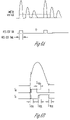
- FIG. 4 shows a sub-harmonic oscillation in a resonant voltage waveform
- FIG. 5 shows an example RDFC according to the present invention
- FIG. 6 a illustrates signal ResEstSig
- FIG. 6 b illustrates extension and blanking periods of signals Sr and Sf
- RDFC resonant discontinuous forward converters.
- power to a primary or input winding of a transformer is switched and a secondary or output winding of the transformer, with a polarity matched to that of the primary winding, is coupled to a rectifier which provides do power to a smoothing capacitor, do power being supplied by the RDFC to its output from this connection node X.
- a voltage waveform on the secondary winding of the transformer has a first portion during which the switch is on current flows into the output connection node X, and second substantially resonant portion during which both the switch and the rectifier are off. Substantially no current flows into the connection node (other than from the smoothing capacitor) during the second portion of the voltage waveform.
- connection between the rectifier and the connection node may include a small inductor (for example less than 5% of the primary side magnetising inductance) but substantially no current flows in this inductance during the second, resonant portion of the waveform and there is no need for a large choke of the type used in a continuous forward converter.
- a capacitor across the rectifier to achieve resonance There is no need connect a capacitor across the rectifier to achieve resonance; other connection positions are possible, for example, across a primary, secondary or auxiliary winding of the transformer. More particularly in embodiments we use the magnetising inductance of the transformer with an added capacitor on the primary side to achieve resonance in the off cycle.
- the RDFC is configured for AC-DC power conversion and thus includes an AC-DC converter such as a bridge rectifier on the primary side.
- the RDFC is mains-powered and the primary side is powered by a high dc voltage (for example greater than 70 Vdc, 100 Vdc, 150 Vdc or 200 Vdc) whilst the secondary side de voltage is low (for example, less than 20 Vdc or 10 Vdc).
- a primary side switch is turned on at a time when a voltage across the switch is close to zero volts.
- RDFC resonant discontinuous forward converter
- the control system may operate in an uncontrolled, fixed frequency mode or the control system may sense from one or more inputs and decide when to turn the power switch on and off responsive to this sensing, for example to implement pulse width and/or frequency modulation.
- This facilitates regulation of the RDFC which, in detail, may be performed using a range of algorithms.
- One technique uses the control system to operate the RDFC to compensate for circuit variables and to operate in a minimum voltage switching mode.
- the converter may also control the switching frequency during start-up and/or current limit in order to protect the power switch and increase the energy transferred to the load.
- the control system is preferably implemented using a control IC (integrated circuit).
- the RDFC operates without a freewheeling or flyback diode, and with or without an output inductor.
- the output inductor is sufficiently small to ensure that the forward converter operates in a discontinuous mode and substantially resonantly that is at or close to resonance.
- the timing of the primary power switch has to be: in accordance with the resonance of the isolating transformer and other components forming part of the resonating circuit; managed to control the power transfer to the output; and appropriate to the other components (particularly the transformer) so they operate without excessive stress and within an efficient range.
- timing is set by a controller, which determines the time to turn the primary switch on and how long to leave it on.
- FIG. 2 shows a basic arrangement of an RDFC 200 , comprising an isolating transformer 202 having primary 202 P and secondary 202 S windings.
- a switch 204 when closed, applies a DC voltage V ht across the primary winding of the transformer.
- Power is delivered to the load 212 via a rectifying diode 208 and smoothing capacitor 210 .
- the polarity of the transformer is such that power is supplied to the output circuit when the primary switch is closed.
- Inductance L leak may be a discrete component or may be a characteristic of the transformer itself, in which case it can be modelled as an inductor in either the primary circuit or the secondary circuit, or both.
- the magnitude of L leak affects the behaviour and performance of the converter. For applications requiring more stable voltage regulation L leak is normally lower in value; for applications requiring a higher converter output impedance (such as battery chargers), its value is set higher.
- Example waveforms of converter operation are shown in FIG. 3 a .
- switch 204 When switch 204 is in the On state, current flows through the switch and transformer primary. The current rises in accordance with load conditions and the effect of L leak . At switch-off, the voltage rises rapidly (reflected load current in L leak ) to point “A”.
- the circuit resonates as the combination of C res 206 and the magnetising inductance of the transformer L mag , and other stray reactances.
- the switch voltage reaches a peak then reduces. Depending on circuit values and conditions, it may reach 0V (“B”).
- the switch voltage may be prevented from resonating below 0V either by diodes associated with the switch, or by the effect of the output diode and voltage on the output capacitor.
- FIG. 3 a shows the switch being turned on at point “B”.
- FIG. 3 b shows example waveforms of the switch being turned on before the resonant waveform reaches point “B”, and
- FIG. 3 c shows the switch being turned on later than point “B”.
- the switch waveform can be seen to oscillate as a damped sinewave around V ht . Switching. Optimum power transfer is achieved by turning the switch on again at point “B”.
- the turn-on instant of the switch is preferably chosen to correspond to a minimum of the resonance of the switch voltage.
- the switch is turned on when the switch voltage is close to 0V (“B” in FIG. 3 a ).
- the switch voltage is close to 0V (“B” in FIG. 3 a ).
- FIG. 3 d is a more detailed view of the waveform shown in FIG. 3 a and shows the main parts of the observed resonance wave.
- the polarity represents the voltage across the power switch assuming a positive supply to the transformer primary and the power switch is connected in the other connection of the primary to the negative supply.
- the three main parts are:
- On-period when the power switch is turned on, connecting the transformer primary to the power source. Voltage across the switch is low. During this period current flow is principally reflected secondary (load-related) current and magnetising current rising according to the primary inductance and supply voltage etc.
- Leakage resonance In this period, current continues to flow in the secondary.
- the primary voltage is a (fast) resonance of the leakage inductance with the resonant capacitance.
- the magnitude of this resonant voltage depends on the current at turn-off and the leakage inductance.
- the former is typically mostly the reflected secondary current, but there may be a small contribution from magnetising current, depending on circuit parameters.
- this resonance is fast and the turnoff time of the switch may be significant so the exact waveform is complex.
- Magnetising resonance Once the secondary current has substantially decayed, the wave results from resonance of the magnetising inductance and the resonant capacitance.
- the amplitude depends on the magnetising current at the end of the on-period which depends on the magnetising current at the beginning of the on-period, the supply voltage and the duration of the on-period etc.
- Typical waveforms are illustrated in FIG. 3 e ; all correspond to the condition where the on-period commences immediately the switch voltage reaches a minimum. Though the on-time and reflected secondary current are not necessarily dependent, in typical applications the on-period is shortened when the secondary current is high, for example in overload.
- At least three operational modes to manage power are identifiable:
- the on-time is reduced before increasing off-time. Reducing the on-time minimises transformer losses, EMI and audible noise, as the core flux is reduced (consequence of reducing on-time). Minimising the off-time allows the on-time to be maximised at medium and high powers, whilst staying within allowable core flux, as this maximises the reverse magnetising current from the previous cycle.
- change of mode is performed on the basis of the measured primary switch current and its rate of rise, but a further choice is the rate at which the controlled parameters (on-time and off-time) are changed in response to the measured current. If the controlled parameters change slowly then the system will also respond slowly to changing conditions, possibly leading to undesirable voltage excursions.
- V switch signal Symptomatically, an alternate high and low voltage resonance is observed in the V switch signal. In extreme cases, these fluctuations may cause damage to the switch in the off-state.
- the off-time it is preferable to adjust the off-time so that it does not solely depend on the resonance of the preceding cycle to suppress this behaviour.
- a resonance time is calculated based on two or more previous converter cycles.
- the off-time is then forced to be the same as this calculated resonance time.
- the subsequent turn-on of the primary switch is therefore set by the calculated resonance time, rather than to the resonant waveform itself, which may reduce the sub-harmonic oscillation in the resonant voltage.
- the resonance time may be calculated in a way that changes slowly from cycle-to-cycle so that, as a minimum, the half-rate subharmonic oscillation is reduced.
- the resonance period is characteristic of a particular resonant system and will vary particularly with transformer primary inductance. This is beneficial because a larger winding inductance generally allows longer on-time within core limitations, other conditions being similar.
- transformer construction limitations Switch voltage limit and other issues such as operating frequency (to avoid audible noise).
- Higher inductance allows longer on-time, which is in accordance with core flux limitation.
- Lower resonating capacitance leads to shorter on-time, which reduces core energy so that peak switch voltage is limited despite reduced capacitance.
- ResEstSig is an estimate of the resonant portion of the primary signal and is derived from the time between a first and second event associated with the switch being switched off. Preferably this is between turn-off of the switch and the first trailing edge of a falling signal (Sf) that represents a portion of the voltage across the switch during which the rate of decrease of the voltage is greater than a falling threshold value. Preferably the measurement is taken using a trailing edge of Sf that coincides with the end of the resonant signal.
- ResEstTime is derived from ResEstSig and is an estimate of the resonance time.
- FIG. 6 a illustrates ResEstSig.
- the or turn-off time of the switch is short or predictable, so any delay in switching is small or can be corrected.
- the leading edge of a rising signal may be used to mark the start of the resonance. Sr represents a portion of the voltage across the switch during which the rate of increase of the voltage is greater than a rising threshold value.
- the next falling edge of Sf can then be used to indicate the end of the resonance for the purpose of resonance estimation.
- FIG. 8 b illustrates extension and blanking periods of signals Sr and Sf.
- a preferred, and simplified solution would be to observe the resonance and determine simply if the resonance completes before or after the current estimate of resonance time. If the resonance completes before the current estimate, then the estimate can be reduced by a small amount. Conversely, if the resonance completes after the estimate, the estimate is increased.
- the resonance estimate will tend to track the actual resonance time, but with an averaging effect and some lag. This may be adequate in applications where the resonance time does not change quickly, but further optional techniques are preferred to handle dynamic conditions:
- An alternative or additional method to suppress sub-harmonic oscillation is to observe the resonant current (through the resonant capacitor, or part thereof) or the integral of the current on a cycle-by cycle basis. Like the resonant time, this gives information about sub-harmonic variations and may be used to adjust the off-time to counteract any oscillatory behaviour.
- the forced off-time can be made up of two components, one equal to the tracked resonance time and a second, smaller, component which depends on the current. It is arranged so that a higher current increases the off-time to attempt to counteract the tendency to oscillation.
- the magnitude of resonant current sensed in one off-period may be used to alter the duration of the subsequent on-period.
- a high resonant current is arranged to cause an increase in duration of the on-period with the objective of stabilising the magnetic energy in the transformer at the end of the on-period.
- the maximum available range of flux in the transformer core limited by the characteristics of the core material.
- the core flux increases (tends to more positive) and reaches a maximum approximately at the end of the on-period.
- On-period is a primary means of control of power delivery, enabling reduction of power in response to light load or overload.
- it is necessary to manage the on-period to ensure that a large, but not excessive, flux range is used.
- the negative flux at the beginning of the on-period may be significant in reducing the peak positive flux at the end of the period. This can cause difficulties when the on-period or off period are changed, because both affect the negative flux at the beginning of the on-period.
- the on-period is increased in one converter cycle compared to the previous, the negative flux at the beginning of the on-period may be insufficient to limit the flux at the end to an acceptable level.
- the increase between cycles may be simply at a fixed predetermined rate or, preferably, at a rate determined from the maximum on-period (itself may be determined from the estimated resonance time), such as a fraction of the maximum on-period.
- control techniques described here may be embodied in a system at low cost with few components.
- an integrated controller device works with a low-cost power bipolar transistor to make an off-line power converter with several commercial advantages, including: high power capability despite small and low-cost components; the use of bipolar power switch transistor rather than the higher-cost alternative of power mosfet or IGBT; compact size; low power loss in low/no-load conditions; and high conversion efficiency.
- FIG. 5 shows an example RDFC 500 with such a controller.
- the RDFC comprises an isolating transformer 502 having primary 502 P and secondary 502 S windings.
- a switch 504 when closed, applies a DC voltage V ht across the primary winding of the transformer.
- Power is delivered to the load 512 via a rectifying diode 508 and smoothing capacitor 510 .
- the polarity of the transformer is such that power is supplied to the output circuit when the primary switch is closed.
- the RDFC further comprises an RDFC controller 540 .
- the controller preferably includes both analog and digital circuits to implement the above-mentioned control functions in accordance with the present invention.
- the controller is fabricated in a low-cost conventional CMOS process.
- the controller 540 is AC coupled to the primary winding of the transformer to sense a primary signal via a resonance capacitor 506 , which also acts as the resonance capacitor for the RDFC. It is particularly advantageous for the capacitor to serve both functions; high voltages typically occur during converter operation and capacitors capable of withstanding them are expensive. Alternatively, two or more capacitors could be employed, one to couple signal to the controller and the other to supplement the resonance. This may be necessary in high power converters where the resonant current is high and unsuitable for applying in its entirety to the controller input.
- the resonance may be coupled to the controller from a winding of the transformer other than the primary winding, the auxiliary winding for example.
- the primary switch current is sensed by a single resistor R cs 520 .
- the controller is configured to provide a drive signal to the primary switch in response to the above-sensed signals.
- Auxiliary power for the controller device and for base current to the primary switch is derived from an additional winding on the converter transformer, shown in this instance operating in a forward mode. This mode is preferred as it minimises the range of auxiliary voltage V aux under conditions of varying duty cycle and load.
- V aux can still lead to high power dissipation, which is undesired, especially in no/low-load conditions.
- the effect of load on V aux is minimised by the construction of the transformer.
- the winding sequence can be constructed (from core outwards): Auxiliary, Primary and then Secondary.
- the secondary winding leakage inductance can be increased by winding over a reduced length of core, in comparison to the width of the primary and auxiliary windings.
- power is preferably taken from the rectified high voltage supply via high value resistor R ht .
Abstract
Description
-
- Amplitude and duration of the leakage resonance increases with the sum of reflected load current and magnetising current. These scale according also to the magnitude of the leakage inductance.
- Amplitude of the magnetising resonance increases with on-period and supply voltage. Duration of the magnetising resonance depends on the magnetising current remaining at the end of the leakage resonance and the voltage at that time.
-
- Maximum power (Maximum on-time and minimum off-time)
- Medium power (Reduced on-time and minimum off-time)
- Low power (Minimum on-time and extended off-time)
Sf(a)=¼ of ResEstTime
Sf(b)= 1/16 of ResEstTime
-
- Start-up: measure the resonance of the first cycle (off-period) and use this value to set the initial resonance estimate
- Resonance very short: if the observed resonance is significantly shorter than the present estimate, either decrease the estimate more quickly (larger change), or set the estimate directly to the observed value
- Resonance very long: if the observed resonance is significantly longer than the present estimate, either increase the estimate more quickly (larger change), or set the estimate directly to the observed value
- Estimate in error for several cycles: if, for several cycles, the resonance is observed to be always late or always early in comparison to the estimate, then increase the rate of change of the estimate.
Claims (20)
Applications Claiming Priority (3)
| Application Number | Priority Date | Filing Date | Title |
|---|---|---|---|
| GB0706256A GB2447874B (en) | 2007-03-30 | 2007-03-30 | Forward power converter controllers |
| GB07062565 | 2007-03-30 | ||
| GB7062565 | 2007-03-30 |
Publications (2)
| Publication Number | Publication Date |
|---|---|
| US20080239761A1 US20080239761A1 (en) | 2008-10-02 |
| US7714554B2 true US7714554B2 (en) | 2010-05-11 |
Family
ID=38050559
Family Applications (1)
| Application Number | Title | Priority Date | Filing Date |
|---|---|---|---|
| US11/732,107 Expired - Fee Related US7714554B2 (en) | 2007-03-30 | 2007-04-02 | Forward power converter controllers |
Country Status (3)
| Country | Link |
|---|---|
| US (1) | US7714554B2 (en) |
| GB (1) | GB2447874B (en) |
| WO (1) | WO2008120013A1 (en) |
Cited By (4)
| Publication number | Priority date | Publication date | Assignee | Title |
|---|---|---|---|---|
| US20080239764A1 (en) * | 2007-03-30 | 2008-10-02 | Cambridge Semiconductor Limited | Forward power converter controllers |
| US20090231889A1 (en) * | 2008-03-14 | 2009-09-17 | Power Integrations, Inc. | Method and apparatus for ac to dc power conversion with reduced harmonic current |
| US20100302811A1 (en) * | 2009-06-02 | 2010-12-02 | Power Integrations, Inc. | Single-stage power supply with power factor correction and constant current output |
| US8975887B2 (en) | 2012-07-08 | 2015-03-10 | R2 Semiconductor, Inc. | Suppressing oscillations in an output of a switched power converter |
Families Citing this family (7)
| Publication number | Priority date | Publication date | Assignee | Title |
|---|---|---|---|---|
| GB2448117B (en) * | 2007-03-30 | 2009-06-03 | Cambridge Semiconductor Ltd | Forward power converter controllers |
| GB2447874B (en) | 2007-03-30 | 2009-07-29 | Cambridge Semiconductor Ltd | Forward power converter controllers |
| GB2453447A (en) | 2007-04-27 | 2009-04-08 | Cambridge Semiconductor Ltd | A protection scheme for a switched-mode power converter |
| GB2448761A (en) | 2007-04-27 | 2008-10-29 | Cambridge Semiconductor Ltd | Protecting a power converter switch |
| US7880396B2 (en) * | 2007-06-14 | 2011-02-01 | Seiko Epson Corporation | Projector device employing ballast with flyback converter |
| FR3020523B1 (en) * | 2014-04-29 | 2016-05-06 | Valeo Systemes De Controle Moteur | ELECTRICAL POWER SUPPLY AND METHOD FOR CONTROLLING AN ELECTRIC POWER SUPPLY |
| CN112671212A (en) * | 2020-12-14 | 2021-04-16 | 珠海格力电器股份有限公司 | Power supply driving method of ionizer, ionizer and air purifier |
Citations (28)
| Publication number | Priority date | Publication date | Assignee | Title |
|---|---|---|---|---|
| US4415959A (en) | 1981-03-20 | 1983-11-15 | Vicor Corporation | Forward converter switching at zero current |
| US4688160A (en) | 1985-12-19 | 1987-08-18 | American Telephone And Telegraph Co., At&T Bell Labs | Single ended forward converter with resonant commutation of magnetizing current |
| US4783727A (en) | 1986-05-14 | 1988-11-08 | Eckhardt Ag | DC/DC converter |
| US4788634A (en) | 1987-06-22 | 1988-11-29 | Massachusetts Institute Of Technology | Resonant forward converter |
| US4888821A (en) | 1988-12-09 | 1989-12-19 | Honeywell Inc. | Synchronization circuit for a resonant flyback high voltage supply |
| US5278748A (en) | 1991-07-12 | 1994-01-11 | Nec Corporation | Voltage-resonant DC-DC converter |
| US5291385A (en) * | 1992-04-02 | 1994-03-01 | Vlt Corporation | Zero-current switching forward power converter operating in damped reverse boost mode |
| US5315533A (en) | 1991-05-17 | 1994-05-24 | Best Power Technology, Inc. | Back-up uninterruptible power system |
| US5424933A (en) | 1994-01-03 | 1995-06-13 | Avionic Instruments, Inc. | Resonant forward converter circuit with control circuit for controlling switching transistor on and off times |
| WO1999019976A1 (en) | 1997-10-11 | 1999-04-22 | Robert Bosch Gmbh | Method for controlling the switching behaviour of the actuator of a forward converter, and forward converter |
| US5986901A (en) | 1998-07-09 | 1999-11-16 | Matsushita Electric Works R&D Laboratory, Inc. | Power factor correction circuit for a power supply |
| US5991172A (en) * | 1996-06-21 | 1999-11-23 | Delta Electronics, Inc. | AC/DC flyback converter with improved power factor and reduced switching loss |
| US6205037B1 (en) | 1999-12-21 | 2001-03-20 | Thomson Licensing S.A. | Overload protection for a switch mode power supply |
| US6249444B1 (en) | 1999-11-01 | 2001-06-19 | Astec International Limited | Offset resonant ZVS forward converter |
| US6252781B1 (en) | 1998-05-26 | 2001-06-26 | Artesyn Technologies, Inc. | Active reset forward converter employing synchronous rectifiers |
| US6295214B1 (en) | 1999-04-02 | 2001-09-25 | Murata Manufacturing Co., Ltd. | Switching power supply unit |
| US6304463B1 (en) | 1999-05-07 | 2001-10-16 | Power-One, Inc. | Single-ended forward converter circuit with quasi-optimal resetting for synchronous rectification |
| US6314010B1 (en) | 2000-02-25 | 2001-11-06 | Compaq Computer Corporation | Slope-based primary feedback to control the off-time of a power supply |
| US6396718B1 (en) | 2000-12-19 | 2002-05-28 | Semiconductor Components Industries Llc | Switch mode power supply using transformer flux sensing for duty cycle control |
| US6760236B2 (en) | 2002-09-04 | 2004-07-06 | Chih-Hung Hsieh | Third winding reset forward converter |
| US20050152160A1 (en) | 2004-01-08 | 2005-07-14 | Fung Sze W. | Switching-type power converter |
| US20050270809A1 (en) | 2002-12-20 | 2005-12-08 | Leader Electronics Inc. | Device and method for converting an ac voltage |
| US20070274108A1 (en) | 2006-05-26 | 2007-11-29 | Russell Jacques | Forward power converters |
| US20080037293A1 (en) | 2006-05-26 | 2008-02-14 | Russell Jacques | Forward power converter controllers |
| US20080239761A1 (en) | 2007-03-30 | 2008-10-02 | Russell Jacques | Forward power converter controllers |
| US20080239764A1 (en) | 2007-03-30 | 2008-10-02 | Cambridge Semiconductor Limited | Forward power converter controllers |
| US20080239762A1 (en) | 2007-03-30 | 2008-10-02 | Cambridge Semiconductor Limited | Forward power converter controllers |
| US7436153B2 (en) | 2004-05-06 | 2008-10-14 | Continuum Electro-Optics, Inc. | Power supply system method of use |
Family Cites Families (4)
| Publication number | Priority date | Publication date | Assignee | Title |
|---|---|---|---|---|
| US5180964A (en) * | 1990-03-28 | 1993-01-19 | Ewing Gerald D | Zero-voltage switched FM-PWM converter |
| US5267138A (en) * | 1992-03-23 | 1993-11-30 | Creos International Ltd. | Driving and clamping power regulation technique for continuous, in-phase, full-duration, switch-mode resonant converter power supply |
| KR960010713B1 (en) * | 1993-08-17 | 1996-08-07 | 삼성전자 주식회사 | Electronic ballast |
| US6888821B2 (en) * | 2003-02-10 | 2005-05-03 | Nokia Corporation | Dynamic media authorization in mobile networks |
-
2007
- 2007-03-30 GB GB0706256A patent/GB2447874B/en not_active Expired - Fee Related
- 2007-04-02 US US11/732,107 patent/US7714554B2/en not_active Expired - Fee Related
-
2008
- 2008-03-27 WO PCT/GB2008/050221 patent/WO2008120013A1/en active Application Filing
Patent Citations (28)
| Publication number | Priority date | Publication date | Assignee | Title |
|---|---|---|---|---|
| US4415959A (en) | 1981-03-20 | 1983-11-15 | Vicor Corporation | Forward converter switching at zero current |
| US4688160A (en) | 1985-12-19 | 1987-08-18 | American Telephone And Telegraph Co., At&T Bell Labs | Single ended forward converter with resonant commutation of magnetizing current |
| US4783727A (en) | 1986-05-14 | 1988-11-08 | Eckhardt Ag | DC/DC converter |
| US4788634A (en) | 1987-06-22 | 1988-11-29 | Massachusetts Institute Of Technology | Resonant forward converter |
| US4888821A (en) | 1988-12-09 | 1989-12-19 | Honeywell Inc. | Synchronization circuit for a resonant flyback high voltage supply |
| US5315533A (en) | 1991-05-17 | 1994-05-24 | Best Power Technology, Inc. | Back-up uninterruptible power system |
| US5278748A (en) | 1991-07-12 | 1994-01-11 | Nec Corporation | Voltage-resonant DC-DC converter |
| US5291385A (en) * | 1992-04-02 | 1994-03-01 | Vlt Corporation | Zero-current switching forward power converter operating in damped reverse boost mode |
| US5424933A (en) | 1994-01-03 | 1995-06-13 | Avionic Instruments, Inc. | Resonant forward converter circuit with control circuit for controlling switching transistor on and off times |
| US5991172A (en) * | 1996-06-21 | 1999-11-23 | Delta Electronics, Inc. | AC/DC flyback converter with improved power factor and reduced switching loss |
| WO1999019976A1 (en) | 1997-10-11 | 1999-04-22 | Robert Bosch Gmbh | Method for controlling the switching behaviour of the actuator of a forward converter, and forward converter |
| US6252781B1 (en) | 1998-05-26 | 2001-06-26 | Artesyn Technologies, Inc. | Active reset forward converter employing synchronous rectifiers |
| US5986901A (en) | 1998-07-09 | 1999-11-16 | Matsushita Electric Works R&D Laboratory, Inc. | Power factor correction circuit for a power supply |
| US6295214B1 (en) | 1999-04-02 | 2001-09-25 | Murata Manufacturing Co., Ltd. | Switching power supply unit |
| US6304463B1 (en) | 1999-05-07 | 2001-10-16 | Power-One, Inc. | Single-ended forward converter circuit with quasi-optimal resetting for synchronous rectification |
| US6249444B1 (en) | 1999-11-01 | 2001-06-19 | Astec International Limited | Offset resonant ZVS forward converter |
| US6205037B1 (en) | 1999-12-21 | 2001-03-20 | Thomson Licensing S.A. | Overload protection for a switch mode power supply |
| US6314010B1 (en) | 2000-02-25 | 2001-11-06 | Compaq Computer Corporation | Slope-based primary feedback to control the off-time of a power supply |
| US6396718B1 (en) | 2000-12-19 | 2002-05-28 | Semiconductor Components Industries Llc | Switch mode power supply using transformer flux sensing for duty cycle control |
| US6760236B2 (en) | 2002-09-04 | 2004-07-06 | Chih-Hung Hsieh | Third winding reset forward converter |
| US20050270809A1 (en) | 2002-12-20 | 2005-12-08 | Leader Electronics Inc. | Device and method for converting an ac voltage |
| US20050152160A1 (en) | 2004-01-08 | 2005-07-14 | Fung Sze W. | Switching-type power converter |
| US7436153B2 (en) | 2004-05-06 | 2008-10-14 | Continuum Electro-Optics, Inc. | Power supply system method of use |
| US20070274108A1 (en) | 2006-05-26 | 2007-11-29 | Russell Jacques | Forward power converters |
| US20080037293A1 (en) | 2006-05-26 | 2008-02-14 | Russell Jacques | Forward power converter controllers |
| US20080239761A1 (en) | 2007-03-30 | 2008-10-02 | Russell Jacques | Forward power converter controllers |
| US20080239764A1 (en) | 2007-03-30 | 2008-10-02 | Cambridge Semiconductor Limited | Forward power converter controllers |
| US20080239762A1 (en) | 2007-03-30 | 2008-10-02 | Cambridge Semiconductor Limited | Forward power converter controllers |
Non-Patent Citations (14)
| Title |
|---|
| "International Application Serial No. PCT/GB2008/050221, International Search Report mailed Aug. 22, 2008", 3 pgs. |
| "International Application Serial No. PCT/GB2008/050222, International Search Report mailed Mar. 25, 2009", 3 pgs. |
| "U.S. Appl. No. 11/732,108, Non-Final Office Action mailed Jun. 22, 2009", 13 pgs. |
| "U.S. Appl. No. 11/732,140 Non Final Office Action Mailed Aug. 3, 2009", 26. |
| "UCC38C42 25-Watt Self-Resonant Reset Forward Converter", Reference Design, © 2002 Texas Instruments Incorporated,(2002),10 pgs. |
| "United Kingdom Search Report for Application No. GB0706256.5, Dated Jun. 14, 2007", 1 Page. |
| Higashi, T., et al., "Voltage-Mode Resonant Forward Converter With Capacitor-Input Filter", IEICE Transactions on Communications, vol. E79-B, No. 1, (1996), 37-44. |
| International Application No. PCT/GB2008/050220, Partial International Search Report, 2 pgs. |
| Jacques, R., et al., "Forward Power Converter Controllers", U.S. Appl. No. 11/732,108, filed Apr. 2, 2007, 45 pgs. |
| Jacques, R., et al., "Forward Power Converter Controllers", U.S. Appl. No. 11/732,140, filed Apr. 2, 2007, 64 pgs. |
| Spiazzi, G., et al., "A New Soft-Switching Forward DC-DC Converter Operating in Discontinuous Conduction Mode", Conference Proceedings, 33rd Annual IEEE Power Electronics Specialists Conference (PESC 2002), (Cairns, Queensland, Australia, Jun. 23-27, 2002),(2002), 1343-1348. |
| United Kingdom Search Report for Application No. GB0706246.6, dated Jun. 14, 2007, 1 pg. |
| United Kingdom Search Report for Application No. GB0706249.0, dated Jun. 7, 2007, 1 pg. |
| United Kingdom Search Report for Application No. GB0706249.0, dated Oct. 18, 2007, 1 pg. |
Cited By (11)
| Publication number | Priority date | Publication date | Assignee | Title |
|---|---|---|---|---|
| US20080239764A1 (en) * | 2007-03-30 | 2008-10-02 | Cambridge Semiconductor Limited | Forward power converter controllers |
| US7830130B2 (en) | 2007-03-30 | 2010-11-09 | Cambridge Semiconductor Limited | Forward power converter controllers |
| US20090231889A1 (en) * | 2008-03-14 | 2009-09-17 | Power Integrations, Inc. | Method and apparatus for ac to dc power conversion with reduced harmonic current |
| US7990127B2 (en) * | 2008-03-14 | 2011-08-02 | Power Integrations, Inc. | Method and apparatus for AC to DC power conversion with reduced harmonic current |
| US20100302811A1 (en) * | 2009-06-02 | 2010-12-02 | Power Integrations, Inc. | Single-stage power supply with power factor correction and constant current output |
| US8098506B2 (en) | 2009-06-02 | 2012-01-17 | Power Integrations, Inc. | Single-stage power supply with power factor correction and constant current output |
| US8305787B2 (en) | 2009-06-02 | 2012-11-06 | Power Integrations, Inc. | Single-stage power supply with power factor correction and constant current output |
| US8537582B2 (en) | 2009-06-02 | 2013-09-17 | Power Integrations, Inc. | Single-stage power supply with power factor correction and constant current output |
| US9263958B2 (en) | 2009-06-02 | 2016-02-16 | Power Integrations, Inc. | Single-stage power supply with power factor correction and constant current output |
| US9621057B2 (en) | 2009-06-02 | 2017-04-11 | Power Integrations, Inc. | Single-stage power supply with power factor correction and constant current output |
| US8975887B2 (en) | 2012-07-08 | 2015-03-10 | R2 Semiconductor, Inc. | Suppressing oscillations in an output of a switched power converter |
Also Published As
| Publication number | Publication date |
|---|---|
| WO2008120013A1 (en) | 2008-10-09 |
| GB2447874B (en) | 2009-07-29 |
| GB2447874A8 (en) | 2008-10-29 |
| GB0706256D0 (en) | 2007-05-09 |
| US20080239761A1 (en) | 2008-10-02 |
| GB2447874A (en) | 2008-10-01 |
Similar Documents
| Publication | Publication Date | Title |
|---|---|---|
| US7714554B2 (en) | Forward power converter controllers | |
| US7830130B2 (en) | Forward power converter controllers | |
| US7751208B2 (en) | Forward power converter controllers | |
| US9991800B2 (en) | Switched mode power supply with efficient operation at light loads and method therefor | |
| KR101555138B1 (en) | Switching Power Converter for Synchronous Rectification Control And Method Of Using The Same | |
| JP5691137B2 (en) | Switching power supply | |
| JP5463759B2 (en) | Switching power supply device and switching power supply control circuit | |
| US9673718B2 (en) | Voltage conversion method and voltage converter | |
| TWI499178B (en) | Two-switch flyback power converters | |
| US20090201705A1 (en) | Energy converting apparatus, and semiconductor device and switching control method used therein | |
| US20070274108A1 (en) | Forward power converters | |
| TWM568411U (en) | Switched mode power supply controller and switched mode power supply | |
| US20080037293A1 (en) | Forward power converter controllers | |
| GB2448741A (en) | Current sensing and overload protection of a switch mode power converter | |
| US20120113686A1 (en) | Virtual parametric high side mosfet driver | |
| WO2009010802A2 (en) | Forward power converters | |
| TWI792036B (en) | Switching power converters, and methods and packaged integrated circuits for controlling the same | |
| EP2190109A1 (en) | Control device for rectifiers of switching converters. | |
| CN111585444A (en) | Switching converter and method for operating a switching converter | |
| JP6908849B2 (en) | Synchronous rectifier circuit and switching power supply | |
| JP2004536546A (en) | Oscillator circuit, converter having such oscillator circuit, and preconditioning device having such converter | |
| JP2004153948A (en) | Switching power supplying arrangement | |
| US20230170786A1 (en) | Driving Control Circuit, Method and Device for Gallium Nitride (GaN) Transistor, and Medium | |
| JP2010068676A (en) | Switching power supply | |
| JP2009240114A (en) | Switching power supply unit |
Legal Events
| Date | Code | Title | Description |
|---|---|---|---|
| AS | Assignment |
Owner name: CAMBRIDGE SEMICONDUCTOR LIMITED, UNITED KINGDOM Free format text: ASSIGNMENT OF ASSIGNORS INTEREST;ASSIGNORS:JACQUES, RUSSELL;RYAN, PAUL;MCKAY, CATRIONA;AND OTHERS;REEL/FRAME:019682/0761;SIGNING DATES FROM 20070522 TO 20070731 Owner name: CAMBRIDGE SEMICONDUCTOR LIMITED,UNITED KINGDOM Free format text: ASSIGNMENT OF ASSIGNORS INTEREST;ASSIGNORS:JACQUES, RUSSELL;RYAN, PAUL;MCKAY, CATRIONA;AND OTHERS;SIGNING DATES FROM 20070522 TO 20070731;REEL/FRAME:019682/0761 |
|
| AS | Assignment |
Owner name: CAMBRIDGE SEMICONDUCTOR LIMITED, UNITED KINGDOM Free format text: DEBENTURE;ASSIGNOR:ETV CAPITAL S.A.;REEL/FRAME:019714/0643 Effective date: 20070803 Owner name: CAMBRIDGE SEMICONDUCTOR LIMITED,UNITED KINGDOM Free format text: DEBENTURE;ASSIGNOR:ETV CAPITAL S.A.;REEL/FRAME:019714/0643 Effective date: 20070803 |
|
| FEPP | Fee payment procedure |
Free format text: PAYOR NUMBER ASSIGNED (ORIGINAL EVENT CODE: ASPN); ENTITY STATUS OF PATENT OWNER: LARGE ENTITY |
|
| FPAY | Fee payment |
Year of fee payment: 4 |
|
| AS | Assignment |
Owner name: POWER INTEGRATIONS, LIMITED, CAYMAN ISLANDS Free format text: NUNC PRO TUNC ASSIGNMENT;ASSIGNOR:CAMBRIDGE SEMICONDUCTOR LIMITED;REEL/FRAME:034859/0458 Effective date: 20150128 |
|
| AS | Assignment |
Owner name: CAMBRIDGE SEMICONDUCTOR LIMITED, UNITED KINGDOM Free format text: RELEASE BY SECURED PARTY;ASSIGNOR:ETV CAPITAL S.A.;REEL/FRAME:034858/0896 Effective date: 20110714 |
|
| AS | Assignment |
Owner name: POWER INTEGRATIONS LIMITED, CAYMAN ISLANDS Free format text: CORRECTIVE ASSIGNMENT TO CORRECT THE ASSIGNEE NAME PREVIOUSLY RECORDED ON REEL 034859 FRAME 0458. ASSIGNOR(S) HEREBY CONFIRMS THE NUNC PRO TUNC ASSIGNMENT;ASSIGNOR:CAMBRIDGE SEMICONDUCTOR LIMITED;REEL/FRAME:035132/0755 Effective date: 20150128 |
|
| XAS | Not any more in us assignment database |
Free format text: CORRECTIVE ASSIGNMENT TO CORRECT THE ASSIGNEE NAME PREVIOUSLY RECORDED ON REEL 034859 FRAME 0458. ASSIGNOR(S) HEREBY CONFIRMS THE NUNC PRO TUNC ASSIGNMENT;ASSIGNOR:CAMBRIDGE SEMICONDUCTOR LIMITED;REEL/FRAME:035132/0755 |
|
| AS | Assignment |
Owner name: POWER INTEGRATIONS, INC., CALIFORNIA Free format text: ASSIGNMENT OF ASSIGNORS INTEREST;ASSIGNOR:POWER INTEGRATIONS, LIMITED;REEL/FRAME:036852/0533 Effective date: 20150102 |
|
| FEPP | Fee payment procedure |
Free format text: PAT HOLDER NO LONGER CLAIMS SMALL ENTITY STATUS, ENTITY STATUS SET TO UNDISCOUNTED (ORIGINAL EVENT CODE: STOL); ENTITY STATUS OF PATENT OWNER: LARGE ENTITY |
|
| FEPP | Fee payment procedure |
Free format text: MAINTENANCE FEE REMINDER MAILED (ORIGINAL EVENT CODE: REM.) |
|
| LAPS | Lapse for failure to pay maintenance fees |
Free format text: PATENT EXPIRED FOR FAILURE TO PAY MAINTENANCE FEES (ORIGINAL EVENT CODE: EXP.) |
|
| STCH | Information on status: patent discontinuation |
Free format text: PATENT EXPIRED DUE TO NONPAYMENT OF MAINTENANCE FEES UNDER 37 CFR 1.362 |