US7652378B2 - Aluminum-based interconnection in bond pad layer - Google Patents
Aluminum-based interconnection in bond pad layer Download PDFInfo
- Publication number
- US7652378B2 US7652378B2 US11/582,129 US58212906A US7652378B2 US 7652378 B2 US7652378 B2 US 7652378B2 US 58212906 A US58212906 A US 58212906A US 7652378 B2 US7652378 B2 US 7652378B2
- Authority
- US
- United States
- Prior art keywords
- layer
- metal
- aluminum
- pad
- horizontal
- Prior art date
- Legal status (The legal status is an assumption and is not a legal conclusion. Google has not performed a legal analysis and makes no representation as to the accuracy of the status listed.)
- Expired - Fee Related, expires
Links
- 229910052782 aluminium Inorganic materials 0.000 title claims abstract description 35
- XAGFODPZIPBFFR-UHFFFAOYSA-N aluminium Chemical compound [Al] XAGFODPZIPBFFR-UHFFFAOYSA-N 0.000 title claims abstract description 35
- 229910052751 metal Inorganic materials 0.000 claims abstract description 79
- 239000002184 metal Substances 0.000 claims abstract description 79
- 238000001465 metallisation Methods 0.000 claims abstract description 58
- RYGMFSIKBFXOCR-UHFFFAOYSA-N Copper Chemical compound [Cu] RYGMFSIKBFXOCR-UHFFFAOYSA-N 0.000 claims abstract description 28
- 229910052802 copper Inorganic materials 0.000 claims abstract description 28
- 239000010949 copper Substances 0.000 claims abstract description 28
- 239000004065 semiconductor Substances 0.000 claims abstract description 23
- 239000000758 substrate Substances 0.000 claims abstract description 17
- 238000002161 passivation Methods 0.000 claims description 13
- 230000004888 barrier function Effects 0.000 claims description 7
- 239000000463 material Substances 0.000 claims description 5
- 229910052581 Si3N4 Inorganic materials 0.000 claims description 3
- XUIMIQQOPSSXEZ-UHFFFAOYSA-N Silicon Chemical compound [Si] XUIMIQQOPSSXEZ-UHFFFAOYSA-N 0.000 claims description 3
- 229910052710 silicon Inorganic materials 0.000 claims description 3
- 239000010703 silicon Substances 0.000 claims description 3
- HQVNEWCFYHHQES-UHFFFAOYSA-N silicon nitride Chemical compound N12[Si]34N5[Si]62N3[Si]51N64 HQVNEWCFYHHQES-UHFFFAOYSA-N 0.000 claims description 3
- 239000004642 Polyimide Substances 0.000 claims description 2
- 229920001721 polyimide Polymers 0.000 claims description 2
- 239000010410 layer Substances 0.000 description 149
- 238000000034 method Methods 0.000 description 26
- 230000008569 process Effects 0.000 description 16
- 230000015572 biosynthetic process Effects 0.000 description 15
- 239000004020 conductor Substances 0.000 description 9
- 238000005530 etching Methods 0.000 description 8
- WFKWXMTUELFFGS-UHFFFAOYSA-N tungsten Chemical compound [W] WFKWXMTUELFFGS-UHFFFAOYSA-N 0.000 description 8
- 239000003989 dielectric material Substances 0.000 description 7
- 238000004519 manufacturing process Methods 0.000 description 7
- 229910052721 tungsten Inorganic materials 0.000 description 5
- 239000010937 tungsten Substances 0.000 description 5
- 238000005229 chemical vapour deposition Methods 0.000 description 4
- VYPSYNLAJGMNEJ-UHFFFAOYSA-N Silicium dioxide Chemical compound O=[Si]=O VYPSYNLAJGMNEJ-UHFFFAOYSA-N 0.000 description 3
- 230000008901 benefit Effects 0.000 description 3
- 230000009977 dual effect Effects 0.000 description 3
- 150000002739 metals Chemical class 0.000 description 3
- 239000000203 mixture Substances 0.000 description 3
- 229910052814 silicon oxide Inorganic materials 0.000 description 3
- KJTLSVCANCCWHF-UHFFFAOYSA-N Ruthenium Chemical compound [Ru] KJTLSVCANCCWHF-UHFFFAOYSA-N 0.000 description 2
- RTAQQCXQSZGOHL-UHFFFAOYSA-N Titanium Chemical compound [Ti] RTAQQCXQSZGOHL-UHFFFAOYSA-N 0.000 description 2
- NRTOMJZYCJJWKI-UHFFFAOYSA-N Titanium nitride Chemical compound [Ti]#N NRTOMJZYCJJWKI-UHFFFAOYSA-N 0.000 description 2
- 229910017052 cobalt Inorganic materials 0.000 description 2
- 239000010941 cobalt Substances 0.000 description 2
- GUTLYIVDDKVIGB-UHFFFAOYSA-N cobalt atom Chemical compound [Co] GUTLYIVDDKVIGB-UHFFFAOYSA-N 0.000 description 2
- 239000002131 composite material Substances 0.000 description 2
- 238000000151 deposition Methods 0.000 description 2
- PCHJSUWPFVWCPO-UHFFFAOYSA-N gold Chemical compound [Au] PCHJSUWPFVWCPO-UHFFFAOYSA-N 0.000 description 2
- 229910052737 gold Inorganic materials 0.000 description 2
- 239000010931 gold Substances 0.000 description 2
- 238000000059 patterning Methods 0.000 description 2
- 238000005240 physical vapour deposition Methods 0.000 description 2
- 238000001020 plasma etching Methods 0.000 description 2
- 229910052707 ruthenium Inorganic materials 0.000 description 2
- 239000000126 substance Substances 0.000 description 2
- 229910052715 tantalum Inorganic materials 0.000 description 2
- GUVRBAGPIYLISA-UHFFFAOYSA-N tantalum atom Chemical compound [Ta] GUVRBAGPIYLISA-UHFFFAOYSA-N 0.000 description 2
- MZLGASXMSKOWSE-UHFFFAOYSA-N tantalum nitride Chemical compound [Ta]#N MZLGASXMSKOWSE-UHFFFAOYSA-N 0.000 description 2
- 239000010936 titanium Substances 0.000 description 2
- 229910052719 titanium Inorganic materials 0.000 description 2
- 229910000838 Al alloy Inorganic materials 0.000 description 1
- 229910016570 AlCu Inorganic materials 0.000 description 1
- 229910000881 Cu alloy Inorganic materials 0.000 description 1
- 230000004075 alteration Effects 0.000 description 1
- 239000003990 capacitor Substances 0.000 description 1
- 230000008859 change Effects 0.000 description 1
- 238000011109 contamination Methods 0.000 description 1
- 230000008021 deposition Effects 0.000 description 1
- 238000009792 diffusion process Methods 0.000 description 1
- 238000001312 dry etching Methods 0.000 description 1
- 238000005516 engineering process Methods 0.000 description 1
- 239000011521 glass Substances 0.000 description 1
- 230000010354 integration Effects 0.000 description 1
- 239000011229 interlayer Substances 0.000 description 1
- 208000037909 invasive meningococcal disease Diseases 0.000 description 1
- 238000010884 ion-beam technique Methods 0.000 description 1
- 150000002500 ions Chemical class 0.000 description 1
- 238000007521 mechanical polishing technique Methods 0.000 description 1
- 229910001092 metal group alloy Inorganic materials 0.000 description 1
- 238000005272 metallurgy Methods 0.000 description 1
- 230000003071 parasitic effect Effects 0.000 description 1
- 230000035515 penetration Effects 0.000 description 1
- 229920002120 photoresistant polymer Polymers 0.000 description 1
- 238000007747 plating Methods 0.000 description 1
- 239000005368 silicate glass Substances 0.000 description 1
- 239000002356 single layer Substances 0.000 description 1
- 229910000679 solder Inorganic materials 0.000 description 1
- 238000004544 sputter deposition Methods 0.000 description 1
- 238000006467 substitution reaction Methods 0.000 description 1
Images


Classifications
-
- H—ELECTRICITY
- H01—ELECTRIC ELEMENTS
- H01L—SEMICONDUCTOR DEVICES NOT COVERED BY CLASS H10
- H01L23/00—Details of semiconductor or other solid state devices
- H01L23/52—Arrangements for conducting electric current within the device in operation from one component to another, i.e. interconnections, e.g. wires, lead frames
- H01L23/522—Arrangements for conducting electric current within the device in operation from one component to another, i.e. interconnections, e.g. wires, lead frames including external interconnections consisting of a multilayer structure of conductive and insulating layers inseparably formed on the semiconductor body
- H01L23/532—Arrangements for conducting electric current within the device in operation from one component to another, i.e. interconnections, e.g. wires, lead frames including external interconnections consisting of a multilayer structure of conductive and insulating layers inseparably formed on the semiconductor body characterised by the materials
- H01L23/53204—Conductive materials
- H01L23/53209—Conductive materials based on metals, e.g. alloys, metal silicides
- H01L23/53228—Conductive materials based on metals, e.g. alloys, metal silicides the principal metal being copper
- H01L23/53238—Additional layers associated with copper layers, e.g. adhesion, barrier, cladding layers
-
- H—ELECTRICITY
- H01—ELECTRIC ELEMENTS
- H01L—SEMICONDUCTOR DEVICES NOT COVERED BY CLASS H10
- H01L23/00—Details of semiconductor or other solid state devices
- H01L23/52—Arrangements for conducting electric current within the device in operation from one component to another, i.e. interconnections, e.g. wires, lead frames
- H01L23/522—Arrangements for conducting electric current within the device in operation from one component to another, i.e. interconnections, e.g. wires, lead frames including external interconnections consisting of a multilayer structure of conductive and insulating layers inseparably formed on the semiconductor body
- H01L23/532—Arrangements for conducting electric current within the device in operation from one component to another, i.e. interconnections, e.g. wires, lead frames including external interconnections consisting of a multilayer structure of conductive and insulating layers inseparably formed on the semiconductor body characterised by the materials
- H01L23/53204—Conductive materials
- H01L23/53209—Conductive materials based on metals, e.g. alloys, metal silicides
- H01L23/53214—Conductive materials based on metals, e.g. alloys, metal silicides the principal metal being aluminium
- H01L23/53223—Additional layers associated with aluminium layers, e.g. adhesion, barrier, cladding layers
-
- H—ELECTRICITY
- H01—ELECTRIC ELEMENTS
- H01L—SEMICONDUCTOR DEVICES NOT COVERED BY CLASS H10
- H01L24/00—Arrangements for connecting or disconnecting semiconductor or solid-state bodies; Methods or apparatus related thereto
- H01L24/01—Means for bonding being attached to, or being formed on, the surface to be connected, e.g. chip-to-package, die-attach, "first-level" interconnects; Manufacturing methods related thereto
- H01L24/02—Bonding areas ; Manufacturing methods related thereto
-
- H—ELECTRICITY
- H01—ELECTRIC ELEMENTS
- H01L—SEMICONDUCTOR DEVICES NOT COVERED BY CLASS H10
- H01L2224/00—Indexing scheme for arrangements for connecting or disconnecting semiconductor or solid-state bodies and methods related thereto as covered by H01L24/00
- H01L2224/01—Means for bonding being attached to, or being formed on, the surface to be connected, e.g. chip-to-package, die-attach, "first-level" interconnects; Manufacturing methods related thereto
- H01L2224/02—Bonding areas; Manufacturing methods related thereto
- H01L2224/04—Structure, shape, material or disposition of the bonding areas prior to the connecting process
- H01L2224/0401—Bonding areas specifically adapted for bump connectors, e.g. under bump metallisation [UBM]
-
- H—ELECTRICITY
- H01—ELECTRIC ELEMENTS
- H01L—SEMICONDUCTOR DEVICES NOT COVERED BY CLASS H10
- H01L2224/00—Indexing scheme for arrangements for connecting or disconnecting semiconductor or solid-state bodies and methods related thereto as covered by H01L24/00
- H01L2224/01—Means for bonding being attached to, or being formed on, the surface to be connected, e.g. chip-to-package, die-attach, "first-level" interconnects; Manufacturing methods related thereto
- H01L2224/02—Bonding areas; Manufacturing methods related thereto
- H01L2224/04—Structure, shape, material or disposition of the bonding areas prior to the connecting process
- H01L2224/04042—Bonding areas specifically adapted for wire connectors, e.g. wirebond pads
-
- H—ELECTRICITY
- H01—ELECTRIC ELEMENTS
- H01L—SEMICONDUCTOR DEVICES NOT COVERED BY CLASS H10
- H01L2224/00—Indexing scheme for arrangements for connecting or disconnecting semiconductor or solid-state bodies and methods related thereto as covered by H01L24/00
- H01L2224/01—Means for bonding being attached to, or being formed on, the surface to be connected, e.g. chip-to-package, die-attach, "first-level" interconnects; Manufacturing methods related thereto
- H01L2224/02—Bonding areas; Manufacturing methods related thereto
- H01L2224/04—Structure, shape, material or disposition of the bonding areas prior to the connecting process
- H01L2224/04073—Bonding areas specifically adapted for connectors of different types
-
- H—ELECTRICITY
- H01—ELECTRIC ELEMENTS
- H01L—SEMICONDUCTOR DEVICES NOT COVERED BY CLASS H10
- H01L24/00—Arrangements for connecting or disconnecting semiconductor or solid-state bodies; Methods or apparatus related thereto
- H01L24/01—Means for bonding being attached to, or being formed on, the surface to be connected, e.g. chip-to-package, die-attach, "first-level" interconnects; Manufacturing methods related thereto
- H01L24/02—Bonding areas ; Manufacturing methods related thereto
- H01L24/04—Structure, shape, material or disposition of the bonding areas prior to the connecting process
- H01L24/05—Structure, shape, material or disposition of the bonding areas prior to the connecting process of an individual bonding area
-
- H—ELECTRICITY
- H01—ELECTRIC ELEMENTS
- H01L—SEMICONDUCTOR DEVICES NOT COVERED BY CLASS H10
- H01L2924/00—Indexing scheme for arrangements or methods for connecting or disconnecting semiconductor or solid-state bodies as covered by H01L24/00
- H01L2924/01—Chemical elements
- H01L2924/01006—Carbon [C]
-
- H—ELECTRICITY
- H01—ELECTRIC ELEMENTS
- H01L—SEMICONDUCTOR DEVICES NOT COVERED BY CLASS H10
- H01L2924/00—Indexing scheme for arrangements or methods for connecting or disconnecting semiconductor or solid-state bodies as covered by H01L24/00
- H01L2924/01—Chemical elements
- H01L2924/01013—Aluminum [Al]
-
- H—ELECTRICITY
- H01—ELECTRIC ELEMENTS
- H01L—SEMICONDUCTOR DEVICES NOT COVERED BY CLASS H10
- H01L2924/00—Indexing scheme for arrangements or methods for connecting or disconnecting semiconductor or solid-state bodies as covered by H01L24/00
- H01L2924/01—Chemical elements
- H01L2924/01014—Silicon [Si]
-
- H—ELECTRICITY
- H01—ELECTRIC ELEMENTS
- H01L—SEMICONDUCTOR DEVICES NOT COVERED BY CLASS H10
- H01L2924/00—Indexing scheme for arrangements or methods for connecting or disconnecting semiconductor or solid-state bodies as covered by H01L24/00
- H01L2924/01—Chemical elements
- H01L2924/01019—Potassium [K]
-
- H—ELECTRICITY
- H01—ELECTRIC ELEMENTS
- H01L—SEMICONDUCTOR DEVICES NOT COVERED BY CLASS H10
- H01L2924/00—Indexing scheme for arrangements or methods for connecting or disconnecting semiconductor or solid-state bodies as covered by H01L24/00
- H01L2924/01—Chemical elements
- H01L2924/01022—Titanium [Ti]
-
- H—ELECTRICITY
- H01—ELECTRIC ELEMENTS
- H01L—SEMICONDUCTOR DEVICES NOT COVERED BY CLASS H10
- H01L2924/00—Indexing scheme for arrangements or methods for connecting or disconnecting semiconductor or solid-state bodies as covered by H01L24/00
- H01L2924/01—Chemical elements
- H01L2924/01027—Cobalt [Co]
-
- H—ELECTRICITY
- H01—ELECTRIC ELEMENTS
- H01L—SEMICONDUCTOR DEVICES NOT COVERED BY CLASS H10
- H01L2924/00—Indexing scheme for arrangements or methods for connecting or disconnecting semiconductor or solid-state bodies as covered by H01L24/00
- H01L2924/01—Chemical elements
- H01L2924/01029—Copper [Cu]
-
- H—ELECTRICITY
- H01—ELECTRIC ELEMENTS
- H01L—SEMICONDUCTOR DEVICES NOT COVERED BY CLASS H10
- H01L2924/00—Indexing scheme for arrangements or methods for connecting or disconnecting semiconductor or solid-state bodies as covered by H01L24/00
- H01L2924/01—Chemical elements
- H01L2924/01033—Arsenic [As]
-
- H—ELECTRICITY
- H01—ELECTRIC ELEMENTS
- H01L—SEMICONDUCTOR DEVICES NOT COVERED BY CLASS H10
- H01L2924/00—Indexing scheme for arrangements or methods for connecting or disconnecting semiconductor or solid-state bodies as covered by H01L24/00
- H01L2924/01—Chemical elements
- H01L2924/01044—Ruthenium [Ru]
-
- H—ELECTRICITY
- H01—ELECTRIC ELEMENTS
- H01L—SEMICONDUCTOR DEVICES NOT COVERED BY CLASS H10
- H01L2924/00—Indexing scheme for arrangements or methods for connecting or disconnecting semiconductor or solid-state bodies as covered by H01L24/00
- H01L2924/01—Chemical elements
- H01L2924/01073—Tantalum [Ta]
-
- H—ELECTRICITY
- H01—ELECTRIC ELEMENTS
- H01L—SEMICONDUCTOR DEVICES NOT COVERED BY CLASS H10
- H01L2924/00—Indexing scheme for arrangements or methods for connecting or disconnecting semiconductor or solid-state bodies as covered by H01L24/00
- H01L2924/01—Chemical elements
- H01L2924/01074—Tungsten [W]
-
- H—ELECTRICITY
- H01—ELECTRIC ELEMENTS
- H01L—SEMICONDUCTOR DEVICES NOT COVERED BY CLASS H10
- H01L2924/00—Indexing scheme for arrangements or methods for connecting or disconnecting semiconductor or solid-state bodies as covered by H01L24/00
- H01L2924/01—Chemical elements
- H01L2924/01078—Platinum [Pt]
-
- H—ELECTRICITY
- H01—ELECTRIC ELEMENTS
- H01L—SEMICONDUCTOR DEVICES NOT COVERED BY CLASS H10
- H01L2924/00—Indexing scheme for arrangements or methods for connecting or disconnecting semiconductor or solid-state bodies as covered by H01L24/00
- H01L2924/01—Chemical elements
- H01L2924/01079—Gold [Au]
-
- H—ELECTRICITY
- H01—ELECTRIC ELEMENTS
- H01L—SEMICONDUCTOR DEVICES NOT COVERED BY CLASS H10
- H01L2924/00—Indexing scheme for arrangements or methods for connecting or disconnecting semiconductor or solid-state bodies as covered by H01L24/00
- H01L2924/013—Alloys
- H01L2924/014—Solder alloys
-
- H—ELECTRICITY
- H01—ELECTRIC ELEMENTS
- H01L—SEMICONDUCTOR DEVICES NOT COVERED BY CLASS H10
- H01L2924/00—Indexing scheme for arrangements or methods for connecting or disconnecting semiconductor or solid-state bodies as covered by H01L24/00
- H01L2924/049—Nitrides composed of metals from groups of the periodic table
- H01L2924/0494—4th Group
- H01L2924/04941—TiN
-
- H—ELECTRICITY
- H01—ELECTRIC ELEMENTS
- H01L—SEMICONDUCTOR DEVICES NOT COVERED BY CLASS H10
- H01L2924/00—Indexing scheme for arrangements or methods for connecting or disconnecting semiconductor or solid-state bodies as covered by H01L24/00
- H01L2924/049—Nitrides composed of metals from groups of the periodic table
- H01L2924/0495—5th Group
- H01L2924/04953—TaN
-
- H—ELECTRICITY
- H01—ELECTRIC ELEMENTS
- H01L—SEMICONDUCTOR DEVICES NOT COVERED BY CLASS H10
- H01L2924/00—Indexing scheme for arrangements or methods for connecting or disconnecting semiconductor or solid-state bodies as covered by H01L24/00
- H01L2924/049—Nitrides composed of metals from groups of the periodic table
- H01L2924/0504—14th Group
- H01L2924/05042—Si3N4
-
- H—ELECTRICITY
- H01—ELECTRIC ELEMENTS
- H01L—SEMICONDUCTOR DEVICES NOT COVERED BY CLASS H10
- H01L2924/00—Indexing scheme for arrangements or methods for connecting or disconnecting semiconductor or solid-state bodies as covered by H01L24/00
- H01L2924/10—Details of semiconductor or other solid state devices to be connected
- H01L2924/11—Device type
- H01L2924/14—Integrated circuits
-
- H—ELECTRICITY
- H01—ELECTRIC ELEMENTS
- H01L—SEMICONDUCTOR DEVICES NOT COVERED BY CLASS H10
- H01L2924/00—Indexing scheme for arrangements or methods for connecting or disconnecting semiconductor or solid-state bodies as covered by H01L24/00
- H01L2924/19—Details of hybrid assemblies other than the semiconductor or other solid state devices to be connected
- H01L2924/1901—Structure
- H01L2924/1904—Component type
- H01L2924/19041—Component type being a capacitor
-
- H—ELECTRICITY
- H01—ELECTRIC ELEMENTS
- H01L—SEMICONDUCTOR DEVICES NOT COVERED BY CLASS H10
- H01L2924/00—Indexing scheme for arrangements or methods for connecting or disconnecting semiconductor or solid-state bodies as covered by H01L24/00
- H01L2924/30—Technical effects
- H01L2924/301—Electrical effects
- H01L2924/30105—Capacitance
-
- H—ELECTRICITY
- H01—ELECTRIC ELEMENTS
- H01L—SEMICONDUCTOR DEVICES NOT COVERED BY CLASS H10
- H01L2924/00—Indexing scheme for arrangements or methods for connecting or disconnecting semiconductor or solid-state bodies as covered by H01L24/00
- H01L2924/30—Technical effects
- H01L2924/301—Electrical effects
- H01L2924/3025—Electromagnetic shielding
Definitions
- This invention relates generally to the fabrication of integrated circuits, and more particularly to the formation of interconnection structures.
- Modern integrated circuits are made up of literally millions of active devices such as transistors and capacitors. These devices are initially isolated from one another, but are later interconnected together to form functional circuits.
- Typical interconnection structures include lateral interconnections, such as metal lines (wirings), and vertical interconnections, such as vias and contacts. Interconnections are increasingly determining the limits of performance and the density of modern integrated circuits.
- dielectrics having low dielectric constants are deposited by either CVD (chemical vapor deposition) or spin-on techniques, and low-resistance metals are patterned to form interconnects using damascene processes, which involve the patterning of trenches in a dielectric layer and the deposition of a metal to fill the trenches and form the metal interconnects. This process may require the overfilling of the trenches. A chemical mechanical polishing technique is then used to remove any excess metal outside the trenches.
- CVD chemical vapor deposition
- spin-on techniques low-resistance metals are patterned to form interconnects using damascene processes, which involve the patterning of trenches in a dielectric layer and the deposition of a metal to fill the trenches and form the metal interconnects. This process may require the overfilling of the trenches.
- a chemical mechanical polishing technique is then used to remove any excess metal outside the trenches.
- bond pads are formed and exposed on the surface of the respective chip. Electrical connections are made through bond pads to connect the chip to a package substrate. Bond pads can be used for wire bonding or flip-chip bonding.
- FIG. 1 is a cross-sectional view of a conventional interconnection structure used in the semiconductor industry.
- an interconnection structure 112 is formed on a substrate 110 , which has integrated circuits (not shown) formed thereon.
- Interconnection structure 112 includes a plurality of metal lines, vias and/or contact plugs. Electrical connections are made through the interconnection structure 112 to a top metallization layer, in which bond pads are formed.
- some of the metal lines may be used to test the devices formed on the substrate 110 .
- a test is performed.
- some of the metal lines such as a metal line 114 , are routed to the edges of the chip and are connected to test pads. Test pads are typically part of the respective metal lines, except the widths of the test pads are greater than the widths of the metal lines.
- the top metallization layer is typically used for forming metal pads and redistribution lines.
- bond pads are distributed throughout the surface of the chip.
- Some of the metal lines, such as line 115 have already been routed to a central region of the chip and is extended to the edge of chip to form a test pad. A via thus can be formed directly connecting the overlying bond pad 120 and the test pad of metal line 115 .
- Other metal lines, such as line 114 are close to the edge of the chip because they are used for test purposes. Therefore, metal line 114 and bond pad 116 are laterally spaced apart, and a redistribution line 118 is needed to redistribute connections from one location on the chip to another.
- the top metallization layer is typically used for forming bond pads and corresponding redistribution lines. Compared to the lower level metallization layers, much fewer connections exist in the top metallization layer, and the usage of the chip area in the top metallization layer is low.
- a semiconductor-metal structure includes a substrate, a copper-based interconnection structure over the substrate, the copper-based interconnection structure comprising a plurality of metallization layers connected by vias and in first dielectric layers, at least one aluminum-based layer over and connected to the copper-based interconnection structure wherein a top layer of the at least one aluminum-based layer comprises a bond pad and an interconnect line connecting to two underlying vias, vias/contacts connecting a top layer of the copper-based interconnection structure and a bottom layer of the at least one aluminum-based layer wherein the vias/contacts are in a second dielectric layer, and a third dielectric layer overlying the at least one aluminum-based layer, wherein the bond pad is exposed through an opening in the third dielectric layer.
- the semiconductor metal structure includes additional aluminum-based metallization layers over the copper-based metallization layers, wherein each aluminum-based metallization layer may include metal lines and interconnect lines.
- a semiconductor-metal structure includes a substrate, an interconnection structure formed over the substrate, the interconnection structure comprising a plurality of metallization layers connected by vias and in first dielectric layers, a metal-pad layer over the interconnection structure, wherein the metal-pad layer comprises a bond pad, an interconnect line and a redistribution line and wherein the interconnect line is not directly connected to a bond pad and is connected to at least two underlying vias/contacts, vias/contacts connecting a top layer of the interconnection structure and the metal-pad layer, wherein the vias/contacts are in a second dielectric layer, and wherein the first dielectric layers and the second dielectric layer have a thickness ratio of less than about 4.
- the semiconductor-metal structure further includes a passivation layer overlying the metal-pad layer, wherein the bond pad is exposed through an opening in the passivation layer.
- interconnect lines formed in the top metallization layer With interconnect lines formed in the top metallization layer, one metallization layer and the respective process steps and masks may be saved. The overall mechanical strength of the respective chip is also improved.
- FIG. 1 illustrates a conventional semiconductor metal structure
- FIGS. 2 through 7B are illustrations of intermediate stages in the manufacture of a preferred embodiment.
- FIG. 8 illustrates a variation of the preferred embodiment comprising more than one aluminum-based metallization layers.
- interconnect line is used to refer to a metal line in the top metal layer, it indicates that the metal line is connected to at least two underlying vias, so that an electrical connection between two underlying electrical features is made.
- FIG. 2 illustrates a substrate 40 , on which integrated circuits (not shown) are formed.
- an inter-layer dielectric ILD, not shown
- Contact plugs are formed through the ILD. Contact plugs are preferably formed by etching contact openings in the ILD and filling the openings with conductive materials, which preferably comprise tungsten, aluminum, copper, or other well-known alternatives. Contact plugs may have composite structures, including, e.g., barrier and adhesion layers.
- a plurality of metallization layers are formed over the ILD to electrically connect and route lower layer metal lines to higher layer metal lines, as well as to interconnect devices and metal lines in lower-level metallization layers. Assuming there are n metallization layers including the layer for forming bond pads, and further assuming the top metallization layer is indicated as layer n, the formation of the metallization layer n ⁇ 1, which is one layer under the top metallization layer, and the top metallization layer n, is discussed hereinafter to explain the concept of the present invention.
- FIGS. 2 through 3B show the formation of a via inter-metal dielectric (IMD) layer 42 over an underlying metallization layer n ⁇ 2 (not shown), followed by the formation of a trench IMD layer 44 on the via IMD layer 42 .
- IMD via inter-metal dielectric
- Trench IMD layer 44 preferably has a low-k value, which is preferably less than about 3.2, while via IMD layer 42 may have k value greater than 3.2 or less than 3.2 depending on process integration and electrical performance.
- the preferred materials include carbon-doped silicon oxide.
- Trench IMD layer 44 and via IMD layer 42 preferably have thicknesses of less than about 2 ⁇ m, and more preferably less than about 15000 ⁇ , and even more preferably between about 3000 ⁇ and 15000 ⁇ .
- the thicknesses may be scaled with the forming technology. For example, if the k values of IMD 44 is greater than about 3.2, a ratio of the thickness of trench IMD layer 44 to the thickness of via IMD 42 may be less than about 1.5, while if the k values of IMD 44 is less than about 3.2, the ratio is preferably less than about 4.
- the methods of forming via IMD layer 42 and trench IMD layer 44 are known in the art, thus the details are not repeated herein.
- dielectric layers 42 and 44 have different etching characteristics, thus an underlying layer may be used as an etch stop/buffer layer when an overlying layer is etched.
- an etch stop/buffer layer (not shown) may be formed between the neighboring IMD layers 42 and 44 , and/or underlying the via IMD layer 42 .
- a single dielectric material is formed and acts as a major portion of both the via IMD layer 42 and the overlying trench IMD layer 44 .
- Via openings 46 and trench openings 48 are then formed, preferably by etching via IMD layer 42 and trench IMD layer 46 , respectively.
- via IMD layer 42 is used as an etch stop/buffer layer for etching trench openings 48 .
- the depth of the trench openings 48 is controlled by adjusting the respective etching time.
- FIG. 3A illustrates the formation of metal lines and the underlying vias.
- a barrier layer (not shown), which preferably comprises titanium, titanium nitride, tantalum, or tantalum nitride, ruthenium-containing conductors, cobalt-containing conductors, wolfram-containing conductors, or combinations thereof, is formed in openings 46 and 48 (refer to FIG. 2 ).
- the barrier layer prevents copper from diffusing into the neighboring IMD layers.
- the remaining space of the via openings 46 and trench openings 48 are filled with conductive materials, preferably copper or copper alloys.
- a chemical mechanical polish (CMP) is performed to remove excess material, leaving metal lines 52 , 56 and 60 and vias 50 , 54 and 58 .
- CMP chemical mechanical polish
- dual damascene processes are preferred for forming metallization layers and vias
- single damascene processes or the combination of dual damascene processes and single damascene processes, can also be used.
- the metal line 52 preferably extends close to an edge 62 of the respective chip.
- An end portion of the metal line 52 is preferably expanded with a greater width, forming a test pad 64 having a pad size, for example, no greater than about 100 ⁇ m*100 ⁇ m, and more preferably no greater than about 70 ⁇ m*70 ⁇ m, such that a metal line (not shown) in an underlying metallization layer may route under the wider test pad for electromagnetic interference (EMI) shielding or metal routing efficiency in circuit design.
- test pads may also be formed in metallization layer n ⁇ 2 (not shown), which is a metallization layer under metallization layer n ⁇ 1, and any underlying metallization layers.
- Metal lines 56 and 60 may be at other locations of the chip.
- FIG. 3B illustrates a top view of the structure shown in FIG. 3A .
- FIG. 4 illustrates the formation of vias/contacts 68 , 70 and 72 .
- vias/contacts 68 , 70 and 72 are copper-based vias formed by a single damascene process, which starts with the formation of a dielectric layer 66 .
- Dielectric layer 66 preferably has a thickness of less than about 20000 ⁇ , and more preferably less than about 15000 ⁇ , and even more preferably between about 1000 ⁇ and about 15000 ⁇ .
- the dielectric layer 66 may have a low-k value, for example, less than about 3.2. However, since fewer metal lines are formed in upper-level metallization layers, the distances between the metal lines and vias in the upper metallization layers are greater than the distances in the lower-level metallization layers, hence the parasitic capacitances between metal features are lower. Therefore, the k value of the dielectric layer 66 may be higher than the underlying dielectric layers for the benefit of improved mechanical strength. In an exemplary embodiment, the k value of the dielectric layer 66 is greater than about 3.2.
- the preferred material of the dielectric layer 66 includes un-doped silicate glass, fluorine-doped silicon oxide, carbon-doped glass, and the like. A ratio of the total thickness of dielectric layer for via/contact portion 66 to the thickness of trench IMD layers 44 is preferably less than about 8, and more preferably less than about 1.5, and even more preferably less than about 1.
- Openings are then formed in the dielectric layer 66 , followed by the formation of a diffusion barrier layer (not shown).
- Vias/contacts 68 , 70 and 72 are then formed in the openings.
- the vias/contacts 68 , 70 and 72 preferably comprise copper, aluminum, tungsten, gold, and the like.
- the vias/contacts 68 , 70 and 72 are contacts comprising tungsten, aluminum, and combinations thereof.
- the structure shown in FIG. 4 may be formed by depositing a metal layer, etching the metal layer to form vias/contacts 68 , 70 and 72 , and forming the dielectric layer 66 .
- FIG. 5 illustrates the formation of a barrier layer 78 , a metal-pad layer 80 and a photoresist 81 , which is then patterned.
- the barrier layer 78 preferably comprises metals having low diffusibility, such as tantalum, tantalum nitride, titanium, titanium nitride, ruthenium-containing conductor, cobalt-containing conductor, wolfram-containing conductor, and the like.
- the metal-pad layer 80 is preferably an aluminum-based metal layer.
- the metal-pad layer 80 comprises AlCu, and may be formed using sputtering, physical vapor deposition (PVD), chemical vapor deposition (CVD), electrochemical copper plating (ECP), and the like.
- the metal-pad layer 80 comprises aluminum, copper, gold, tungsten, or other commonly used metals and metal alloys.
- the thickness of the metal-pad layer 80 is preferably greater than about 3000 ⁇ .
- the optimum thickness (and the width of metal lines formed by patterning the metal-pad layer 80 ) are determined based on the current-carrying ability.
- the sheet resistance of the metal-pad layer 80 is substantially close to the sheet resistance of the underlying metallization layer n ⁇ 1.
- the stacked layers 78 and 80 are then etched, and a resulting structure is shown in FIG. 6A .
- the preferred etching methods include dry etching such as reactive ion etching (RIE) and ion beam bombardment.
- RIE reactive ion etching
- the remaining portions of the metal-pad layer 80 form a redistribution line 82 and an interconnect line 84 , which connects two vias/contacts 70 and 72 .
- vias 68 , 70 and 72 and redistribution line 82 , as well as interconnect line 84 may be formed using a damascene process.
- features 68 , 70 , 72 , 82 and 84 preferably comprise wolfram, aluminum-based conductor, copper, and combination thereof. The resulting structure is shown in FIG. 6B .
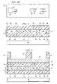
- FIG. 7A illustrates the formation of a passivation layer 86 , which is used for preventing moisture penetration and foreign ion contamination.
- the passivation layer 86 preferably comprises materials such as silicon oxide, silicon oxynitride (SiON), polyimide, silicon nitride (SiN), silicon oxycarbide (SiOC), and the like.
- the passivation layer 86 may also have a composite structure including more than one layer, each formed of a dielectric material.
- An opening is formed in the passivation layer 86 to expose a portion of the redistribution line 82 and to form a bond pad 88 .
- Bond pad 88 may be a pad solely for bonding purpose, or a dual-zone pad including a first zone and a second zone, in which the first zone is for circuit probing and the second zone is for wire-bonding or solder bump attachment.
- the interconnect line 84 is used for interconnecting vias 70 and 72 only, it is preferably completely covered by the passivation layer 86 . However, if desired, a portion 90 of the passivation layer 86 may be removed to expose the underlying interconnect line 84 and to form a bond pad.
- FIG. 7B A top view of FIG. 7A is shown in FIG. 7B , wherein the cross-sectional view in FIG. 8A is taken from a plane crossing a line A-A′ in FIG. 7B .
- Bond pads 88 which are symbolized by circles, are arranged in columns and rows. It can be found that some of the bond pads 88 are directly connected to the underlying vias, which are shown as squares, while other bond pads 88 are connected to the underlying vias through redistribution lines 82 .
- FIG. 8 A further embodiment of the present invention is shown in FIG. 8 .
- metallization layers m through n are all formed with aluminum or aluminum alloys. These layers may be formed layer by layer by forming an aluminum-containing layer, etching the aluminum-containing layer to form desired conductive features, and filling vacancies between the conductive features with a dielectric material.
- the underlying vias/contacts may be copper-based vias or contacts containing aluminum and/or tungsten.
- the metallization layers under the metallization layer m are preferably copper-based and are formed using commonly used damascene processes with copper.
- Each of the metallization layers m through n may include metal lines and interconnect lines. Particularly, interconnect lines are formed in the top metallization layer n.
- the aluminum-based metal lines can also be used as test pads.
- dielectric materials with relatively high-k values can be used as the IMDs to improve the mechanical property of the overall structure, although low-k dielectric materials can also be used.
- the top metallization layer n is used to form interconnect lines in addition to its conventional usage for forming bond pads and redistribution lines.
- the usage of the top metallization layer is thus increased, and one metallization layer may be saved.
- the cost and process steps for forming one metallization layer and the underlying via layer are saved.
- the mechanical strength of the overall structure is improved.
- the preferred embodiments of the present invention require no change to existing process steps.
Abstract
Description
Claims (19)
Priority Applications (1)
| Application Number | Priority Date | Filing Date | Title |
|---|---|---|---|
| US11/582,129 US7652378B2 (en) | 2006-10-17 | 2006-10-17 | Aluminum-based interconnection in bond pad layer |
Applications Claiming Priority (1)
| Application Number | Priority Date | Filing Date | Title |
|---|---|---|---|
| US11/582,129 US7652378B2 (en) | 2006-10-17 | 2006-10-17 | Aluminum-based interconnection in bond pad layer |
Publications (2)
| Publication Number | Publication Date |
|---|---|
| US20080185724A1 US20080185724A1 (en) | 2008-08-07 |
| US7652378B2 true US7652378B2 (en) | 2010-01-26 |
Family
ID=39675462
Family Applications (1)
| Application Number | Title | Priority Date | Filing Date |
|---|---|---|---|
| US11/582,129 Expired - Fee Related US7652378B2 (en) | 2006-10-17 | 2006-10-17 | Aluminum-based interconnection in bond pad layer |
Country Status (1)
| Country | Link |
|---|---|
| US (1) | US7652378B2 (en) |
Cited By (4)
| Publication number | Priority date | Publication date | Assignee | Title |
|---|---|---|---|---|
| US20090075473A1 (en) * | 2007-09-17 | 2009-03-19 | Jung-Bae Kim | Method for fabricating semiconductor device |
| US20150262933A1 (en) * | 2014-03-13 | 2015-09-17 | Taiwan Semiconductor Manufacturing Company Limited | Semiconductor arrangement and formation thereof |
| US20150294939A1 (en) * | 2014-04-14 | 2015-10-15 | Taiwan Semiconductor Manufacturing Company, Ltd. | Packages and Packaging Methods for Semiconductor Devices, and Packaged Semiconductor Devices |
| US9991189B2 (en) * | 2016-07-29 | 2018-06-05 | Taiwan Semiconductor Manufacturing Company, Ltd. | Semiconductor device having a dual material redistribution line |
Families Citing this family (12)
| Publication number | Priority date | Publication date | Assignee | Title |
|---|---|---|---|---|
| US8431473B2 (en) * | 2011-07-07 | 2013-04-30 | United Microelectronics Corp. | Method for fabricating semiconductor device |
| US9093432B2 (en) * | 2011-09-23 | 2015-07-28 | Sanken Electric Co., Ltd. | Semiconductor device |
| US8710660B2 (en) | 2012-07-20 | 2014-04-29 | Taiwan Semiconductor Manufacturing Company, Ltd. | Hybrid interconnect scheme including aluminum metal line in low-k dielectric |
| CN107887285A (en) * | 2016-09-30 | 2018-04-06 | 中芯国际集成电路制造(北京)有限公司 | Welding pad structure and its manufacture method and imaging sensor |
| US10541218B2 (en) * | 2016-11-29 | 2020-01-21 | Taiwan Semiconductor Manufacturing Company, Ltd. | Redistribution layer structure and fabrication method therefor |
| JP2018166171A (en) * | 2017-03-28 | 2018-10-25 | ルネサスエレクトロニクス株式会社 | Method of manufacturing semiconductor device, semiconductor device and inspection equipment for semiconductor device |
| US10515874B2 (en) | 2017-11-30 | 2019-12-24 | Taiwan Semiconductor Manufacturing Company, Ltd. | Semiconductor device and method of manufacture |
| TWI681537B (en) * | 2019-05-30 | 2020-01-01 | 旺宏電子股份有限公司 | Semiconductor structure and method of fabricating wiring structure |
| US11264343B2 (en) * | 2019-08-30 | 2022-03-01 | Taiwan Semiconductor Manufacturing Co., Ltd. | Bond pad structure for semiconductor device and method of forming same |
| US11784151B2 (en) * | 2020-07-22 | 2023-10-10 | Qualcomm Incorporated | Redistribution layer connection |
| KR20220033207A (en) * | 2020-09-09 | 2022-03-16 | 삼성전자주식회사 | A semiconductor chip and a semiconductor package including the same |
| US20230062465A1 (en) * | 2021-09-02 | 2023-03-02 | Tokyo Electron Limited | Bonding layer and process of making |
Citations (10)
| Publication number | Priority date | Publication date | Assignee | Title |
|---|---|---|---|---|
| US5785236A (en) | 1995-11-29 | 1998-07-28 | Advanced Micro Devices, Inc. | Advanced copper interconnect system that is compatible with existing IC wire bonding technology |
| US6114259A (en) * | 1999-07-27 | 2000-09-05 | Lsi Logic Corporation | Process for treating exposed surfaces of a low dielectric constant carbon doped silicon oxide dielectric material to protect the material from damage |
| US6329494B1 (en) | 1998-10-30 | 2001-12-11 | Hitachi Chemical Dupont Microsystems Ltd. | Photosensitive resin composition |
| US6593222B2 (en) * | 2001-09-07 | 2003-07-15 | Lattice Corporation | Method to improve the reliability of thermosonic gold to aluminum wire bonds |
| US6638796B2 (en) | 2002-02-13 | 2003-10-28 | Taiwan Semiconductor Manufacturing Company | Method of forming a novel top-metal fuse structure |
| US6777318B2 (en) | 2002-08-16 | 2004-08-17 | Taiwan Semiconductor Manufacturing Company | Aluminum/copper clad interconnect layer for VLSI applications |
| US6825541B2 (en) | 2002-10-09 | 2004-11-30 | Taiwan Semiconductor Manufacturing Co., Ltd | Bump pad design for flip chip bumping |
| US20050067709A1 (en) * | 2003-09-30 | 2005-03-31 | Bachman Mark Adam | Methods and system for reinforcing a bond pad |
| US20050104187A1 (en) | 2003-10-31 | 2005-05-19 | Polsky Cynthia H. | Redistribution of substrate interconnects |
| US20050200023A1 (en) | 1998-12-21 | 2005-09-15 | Mou-Shiung Lin | Top layers of metal for high performance IC's |
-
2006
- 2006-10-17 US US11/582,129 patent/US7652378B2/en not_active Expired - Fee Related
Patent Citations (11)
| Publication number | Priority date | Publication date | Assignee | Title |
|---|---|---|---|---|
| US5785236A (en) | 1995-11-29 | 1998-07-28 | Advanced Micro Devices, Inc. | Advanced copper interconnect system that is compatible with existing IC wire bonding technology |
| US6329494B1 (en) | 1998-10-30 | 2001-12-11 | Hitachi Chemical Dupont Microsystems Ltd. | Photosensitive resin composition |
| US20050200023A1 (en) | 1998-12-21 | 2005-09-15 | Mou-Shiung Lin | Top layers of metal for high performance IC's |
| US6114259A (en) * | 1999-07-27 | 2000-09-05 | Lsi Logic Corporation | Process for treating exposed surfaces of a low dielectric constant carbon doped silicon oxide dielectric material to protect the material from damage |
| US6593222B2 (en) * | 2001-09-07 | 2003-07-15 | Lattice Corporation | Method to improve the reliability of thermosonic gold to aluminum wire bonds |
| US6638796B2 (en) | 2002-02-13 | 2003-10-28 | Taiwan Semiconductor Manufacturing Company | Method of forming a novel top-metal fuse structure |
| US6831349B2 (en) | 2002-02-13 | 2004-12-14 | Taiwan Semiconductor Manufacturing Co., Ltd. | Method of forming a novel top-metal fuse structure |
| US6777318B2 (en) | 2002-08-16 | 2004-08-17 | Taiwan Semiconductor Manufacturing Company | Aluminum/copper clad interconnect layer for VLSI applications |
| US6825541B2 (en) | 2002-10-09 | 2004-11-30 | Taiwan Semiconductor Manufacturing Co., Ltd | Bump pad design for flip chip bumping |
| US20050067709A1 (en) * | 2003-09-30 | 2005-03-31 | Bachman Mark Adam | Methods and system for reinforcing a bond pad |
| US20050104187A1 (en) | 2003-10-31 | 2005-05-19 | Polsky Cynthia H. | Redistribution of substrate interconnects |
Cited By (9)
| Publication number | Priority date | Publication date | Assignee | Title |
|---|---|---|---|---|
| US20090075473A1 (en) * | 2007-09-17 | 2009-03-19 | Jung-Bae Kim | Method for fabricating semiconductor device |
| US20150262933A1 (en) * | 2014-03-13 | 2015-09-17 | Taiwan Semiconductor Manufacturing Company Limited | Semiconductor arrangement and formation thereof |
| US9646928B2 (en) * | 2014-03-13 | 2017-05-09 | Taiwan Semiconductor Manufacturing Company Limited | Semiconductor arrangement and formation thereof |
| US20150294939A1 (en) * | 2014-04-14 | 2015-10-15 | Taiwan Semiconductor Manufacturing Company, Ltd. | Packages and Packaging Methods for Semiconductor Devices, and Packaged Semiconductor Devices |
| US10074631B2 (en) * | 2014-04-14 | 2018-09-11 | Taiwan Semiconductor Manufacturing Company | Packages and packaging methods for semiconductor devices, and packaged semiconductor devices |
| US10658337B2 (en) * | 2014-04-14 | 2020-05-19 | Taiwan Semiconductor Manufacturing Company | Packages and packaging methods for semiconductor devices, and packaged semiconductor devices |
| US9991189B2 (en) * | 2016-07-29 | 2018-06-05 | Taiwan Semiconductor Manufacturing Company, Ltd. | Semiconductor device having a dual material redistribution line |
| US10811314B2 (en) | 2016-07-29 | 2020-10-20 | Taiwan Semiconductor Manufacturing Company, Ltd. | Method of forming semiconductor device having a dual material redistribution line |
| US11410882B2 (en) | 2016-07-29 | 2022-08-09 | Taiwan Semiconductor Manufacturing Company, Ltd. | Method of forming semiconductor device having a dual material redistribution line and semiconductor device |
Also Published As
| Publication number | Publication date |
|---|---|
| US20080185724A1 (en) | 2008-08-07 |
Similar Documents
| Publication | Publication Date | Title |
|---|---|---|
| US7652378B2 (en) | Aluminum-based interconnection in bond pad layer | |
| US11296011B2 (en) | Through-substrate vias with improved connections | |
| US9978708B2 (en) | Wafer backside interconnect structure connected to TSVs | |
| US9966336B2 (en) | Hybrid interconnect scheme and methods for forming the same | |
| KR101163974B1 (en) | Routing under bond pad for the replacement of an interconnect layer | |
| US8034708B2 (en) | Structure and process for the formation of TSVs | |
| US7397125B2 (en) | Semiconductor device with bonding pad support structure | |
| US8486823B2 (en) | Methods of forming through via | |
| US7514354B2 (en) | Methods for forming damascene wiring structures having line and plug conductors formed from different materials | |
| US20110248404A1 (en) | Dummy Pattern in Wafer Backside Routing | |
| CN101656229A (en) | Semiconductor device and a method of manufacturing the same | |
| US7202565B2 (en) | Semiconductor device which employs an interlayer insulating film of a low mechanical strength and a highly reliable metal pad, and a method of manufacturing the same | |
| US20070120264A1 (en) | A semiconductor having a copper-based metallization stack with a last aluminum metal line layer |
Legal Events
| Date | Code | Title | Description |
|---|---|---|---|
| AS | Assignment |
Owner name: TAIWAN SEMICONDUCTOR MANUFACTURING COMPANY, LTD., Free format text: ASSIGNMENT OF ASSIGNORS INTEREST;ASSIGNORS:TSENG, HORNG-HUEI;HU, CHENMING;REEL/FRAME:018913/0297;SIGNING DATES FROM 20070201 TO 20070206 |
|
| STCF | Information on status: patent grant |
Free format text: PATENTED CASE |
|
| FPAY | Fee payment |
Year of fee payment: 4 |
|
| FPAY | Fee payment |
Year of fee payment: 8 |
|
| FEPP | Fee payment procedure |
Free format text: MAINTENANCE FEE REMINDER MAILED (ORIGINAL EVENT CODE: REM.); ENTITY STATUS OF PATENT OWNER: LARGE ENTITY |
|
| LAPS | Lapse for failure to pay maintenance fees |
Free format text: PATENT EXPIRED FOR FAILURE TO PAY MAINTENANCE FEES (ORIGINAL EVENT CODE: EXP.); ENTITY STATUS OF PATENT OWNER: LARGE ENTITY |
|
| STCH | Information on status: patent discontinuation |
Free format text: PATENT EXPIRED DUE TO NONPAYMENT OF MAINTENANCE FEES UNDER 37 CFR 1.362 |
|
| FP | Lapsed due to failure to pay maintenance fee |
Effective date: 20220126 |